enhanced control for local helicity injection on the ...€¦ · layout slide (include for posters)...
TRANSCRIPT

PEGASUSToroidal Experiment
University ofWisconsin-Madison
59th Annual Meeting of the APS
Division of Plasma Physics
26 October 2017
Milwaukee, WI
Enhanced Control for Local Helicity Injection on the Pegasus ST
C. Pierren,
M.W. Bongard, R.J. Fonck, B.T. Lewicki, J.M. Perry
2
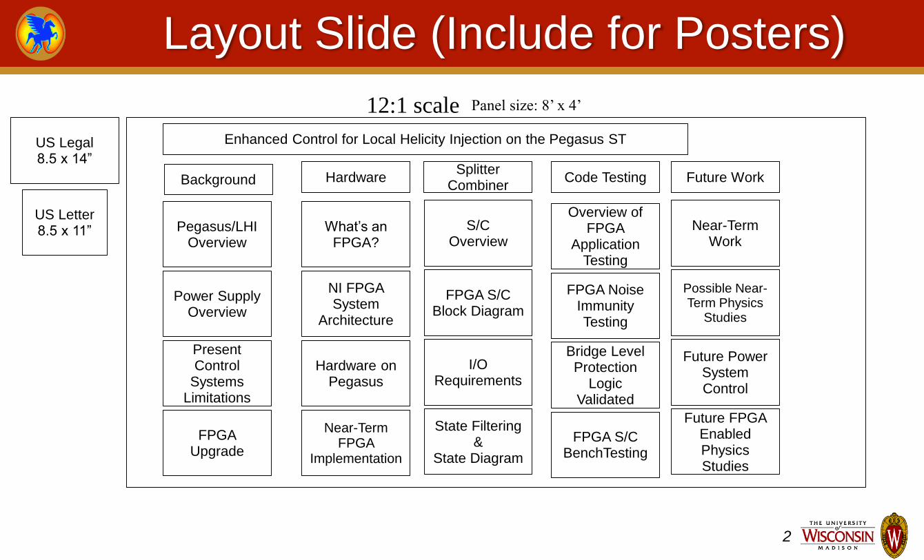
Layout Slide (Include for Posters)
US Legal8.5 x 14”
US Letter8.5 x 11”
Panel size: 8’ x 4’12:1 scale
Power Supply Overview
PresentControl
Systems Limitations
FPGA Upgrade
Pegasus/LHI Overview
NI FPGA System
Architecture
Hardware on Pegasus
Near-Term FPGA
Implementation
What’s an FPGA?
FPGA Noise Immunity Testing
Bridge Level Protection
Logic Validated
FPGA S/C BenchTesting
Overview of FPGA
Application Testing
Possible Near-Term Physics
Studies
Future Power System Control
Future FPGA Enabled Physics Studies
Near-Term Work
FPGA S/C Block Diagram
I/O Requirements
State Filtering &
State Diagram
S/COverview
Enhanced Control for Local Helicity Injection on the Pegasus ST
Background Hardware Code Testing Future WorkSplitter
Combiner
3
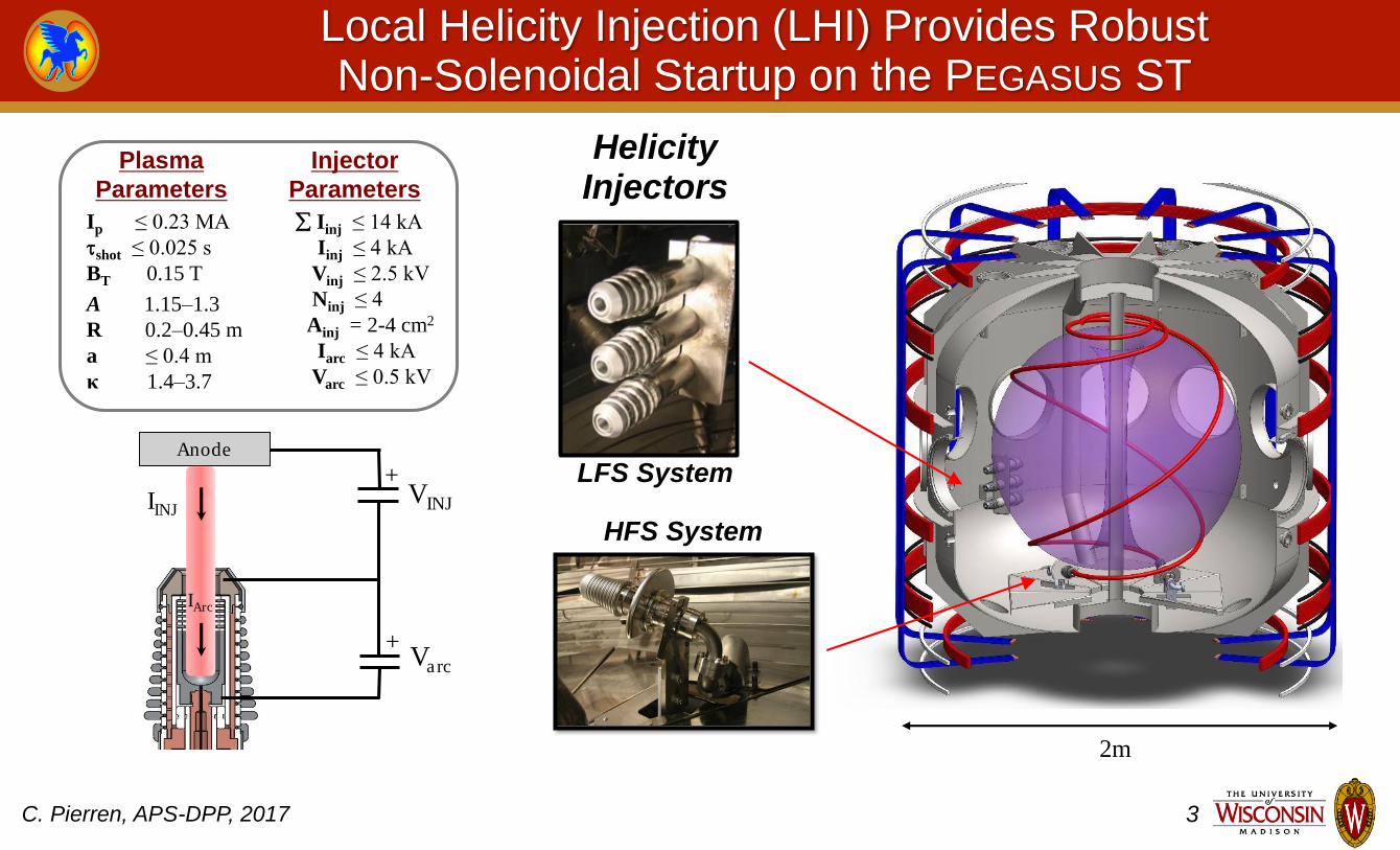
Local Helicity Injection (LHI) Provides Robust Non-Solenoidal Startup on the PEGASUS ST
C. Pierren, APS-DPP, 2017
Plasma
Parameters
Ip ≤ 0.23 MA
tshot ≤ 0.025 s
BT 0.15 T
A 1.15–1.3
R 0.2–0.45 m
a ≤ 0.4 m
κ 1.4–3.7
Injector
Parameters
Iinj ≤ 14 kA
Iinj ≤ 4 kA
Vinj ≤ 2.5 kV
Ninj ≤ 4
Ainj = 2-4 cm2
Iarc ≤ 4 kA
Varc ≤ 0.5 kV
Anode
VINJ
+
Varc
+
IINJ
IArc
HelicityInjectors
HFS System
LFS System
2m

4
Pegasus Driven by ~ 250 MVA Modular Power System
• Drive wide range of loads
• 35 optically isolated H-Bridges
– 12 IGCT
– 23 IGBT
• Analog feedback control
• Control signals multiplexed to N bridges
– ‘Splitter-Combiner’ (S/C)
C. Pierren, APS-DPP, 2017
Load TypesOperating
Voltage𝑰𝒎𝒂𝒙[kA]
Controlled Power
[MVA]
Toroidal Field (TF) 900 24 21.6
Poloidal Field (PF) (x3) 900 16 14.4
Radial Coil 900 4 3.6
Divertor Coil 900 4 3.6
Ohmic Solenoid 2200 32 70.4
Injector Arc (x4) 900 4 3.6
Injector Bias (x2) 2200 12 26.4
IGCT
IGBT

5
Next Generation LHI Enabled by Planned Power Supply and Control System Upgrades
• FPGA ‘Splitter-Combiner’
– Expands number of simultaneously controllable bridges
– Improve IGCT Protections
• Ćuk Converter Power Supply for Injector Arc & Bias
– Low ripple programmable voltage control
• FPGA Digital Feedback Controllers
– Programmable coil set and helicity injection control
• Increase TF (H-Bridge)
– Increased Taylor Limit, confinement studies
• Expand PF (H-Bridge)
– Improved position and shaping control
C. Pierren, APS-DPP, 2017
H-Bridge Topology (1 of 35)
Ćuk Converter (Planned)
https://en.wikipedia.org/wiki/%C4%86uk_converter

6
FPGA Digital Splitter-Combiner (S/C) and Feedback Controller Expand Pegasus Control Capabilities
C. Pierren, APS-DPP, 2017
• Benefits of FPGA:
– Programmable control algorithms
– Expandable with off-the-shelf hardware
– Improved EMI resilience
– Increased stability (e.g. no comparator drift)
• S/C Improvements:
– Additional device-level protections
– Reduced fault response time
– Continuous fault monitoring
Planned FPGA Control
Present Analog Control

7
Field Programmable Gate Array (FPGA) Technology Overview
C. Pierren, APS-DPP, 2017
• “Programmable hardware” via low-level logic descriptor languages (VHDL) or high-level (LabVIEW FPGA)
• Input / output interfaces
– Analog and Digital I/O
• Clocks / timers
– 10, 40 MHz fundamental
• Direct Memory Access (DMA) interfaces
– FPGA↔Realtime PC data exchange
• PCI, PXI bus interfaces
– Inter-FPGA signaling, data exchange, timing
I/O Blocks
ProgrammableInterconnects
LogicBlocks
FPGA Resource Types
Source: NI.com, Introduction to LabView Real-Time and FPGA
https://forums.ni.com/t5/Community-Documents/Introduction-to-LabVIEW-Real-Time-and-FPGA-Presentation-and/ta-p/3515914
8
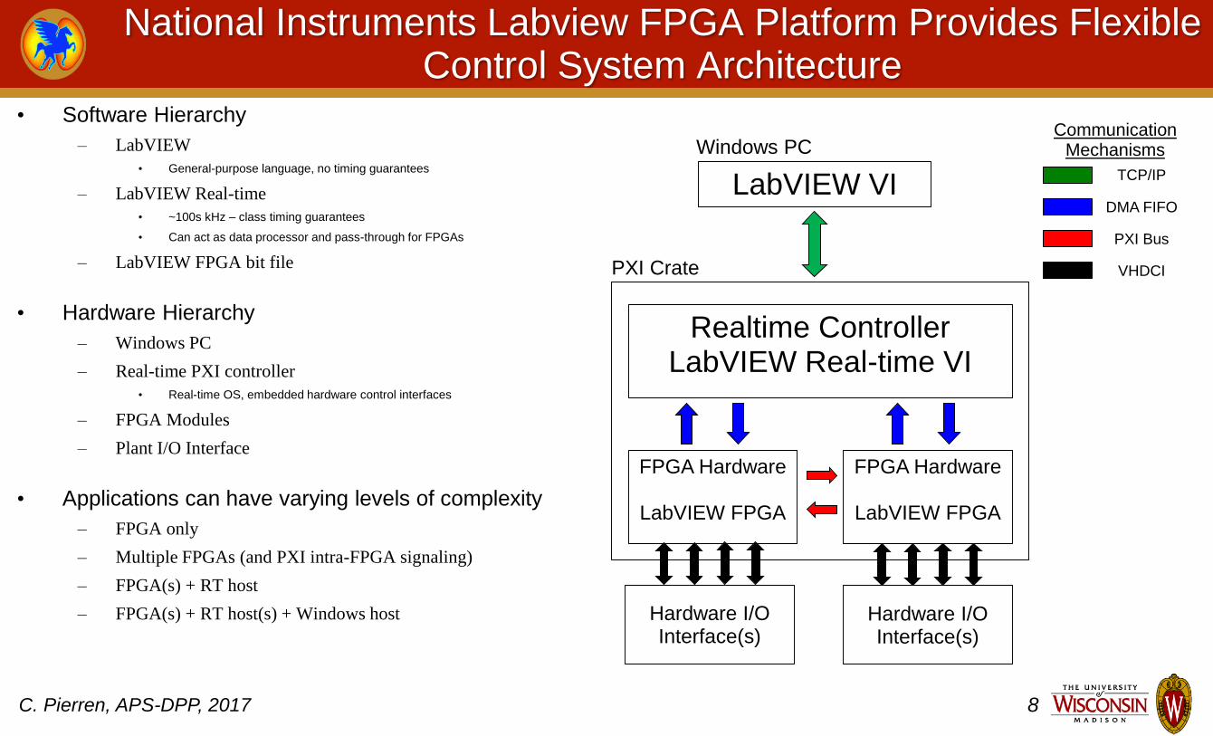
National Instruments Labview FPGA Platform Provides Flexible Control System Architecture
C. Pierren, APS-DPP, 2017
• Software Hierarchy
– LabVIEW
• General-purpose language, no timing guarantees
– LabVIEW Real-time
• ~100s kHz – class timing guarantees
• Can act as data processor and pass-through for FPGAs
– LabVIEW FPGA bit file
• Hardware Hierarchy
– Windows PC
– Real-time PXI controller
• Real-time OS, embedded hardware control interfaces
– FPGA Modules
– Plant I/O Interface
• Applications can have varying levels of complexity
– FPGA only
– Multiple FPGAs (and PXI intra-FPGA signaling)
– FPGA(s) + RT host
– FPGA(s) + RT host(s) + Windows host
CommunicationMechanisms
TCP/IP
DMA FIFO
PXI Bus
VHDCI
LabVIEW VI
Realtime ControllerLabVIEW Real-time VI
FPGA Hardware
LabVIEW FPGA
PXI Crate
FPGA Hardware
LabVIEW FPGA
Hardware I/OInterface(s)
Hardware I/OInterface(s)
Windows PC

9
FPGA Hardware Employed for Pegasus System
C. Pierren, APS-DPP, 2017
• NI PXI 7852R “Hybrid” FPGA (x2)
– 8 AI, 8 AO
– 96 DIO
• NI PXI 7813R “Digital” FPGA (x1)
– 160 DIO channels
• PXIe-1062Q Crate (x2)
– Houses embedded controller (PXIe-8133 / PXIe-
8135) and FPGA units
– Real-time LabVIEW control capability
– TCP/IP remote control capability
• Electro Standards Laboratory (ESL) Custom TTL↔Optical Transceiver (x7)
– Convert 20 TTL I/O pairs to 20 Optical TX/RX pairs
– Optical signaling compatible with IGBTs & IGCTs
NI 7852R Hybrid FPGA NI 7813R Digital FPGA
NI 8133 PXIe Controller NI PXIe-1062Q Crate
ESL TTL↔Fiber Transceiver(front and back connectors)

10
FPGA Splitter-Combiner Chosen as First Application
• Addresses technical requirements for many applications:
– Fundamental for planned upgrades
• Improvements enabled by FPGA S/C:
– Continuous fault monitoring
– Improved fault response time
– More robust device protection
– Increased number of controllable bridges
C. Pierren, APS-DPP, 2017
H-Bridge1
CoilLoad
H-BridgeN
PWMDemand
Generator
Rogowski
C
∑ Fi
FNCF1C
Splitter/Combiner
● ● ●
PSD
DAS
PWM_i Demand
Open-loop Demands
S/C Block Replacement
11
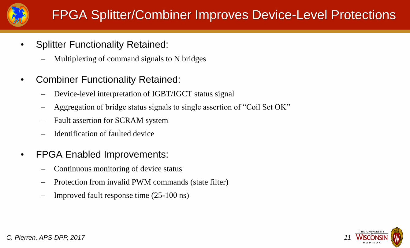
FPGA Splitter/Combiner Improves Device-Level Protections
C. Pierren, APS-DPP, 2017
• Splitter Functionality Retained:
– Multiplexing of command signals to N bridges
• Combiner Functionality Retained:
– Device-level interpretation of IGBT/IGCT status signal
– Aggregation of bridge status signals to single assertion of “Coil Set OK”
– Fault assertion for SCRAM system
– Identification of faulted device
• FPGA Enabled Improvements:
– Continuous monitoring of device status
– Protection from invalid PWM commands (state filter)
– Improved fault response time (25-100 ns)

12
FPGA Splitter-Combiner Block Diagram
C. Pierren, APS-DPP, 2017
Initialization Input State Filter Splitters
Combiners
(IGBT,IGCT)
Q Signal Input
Status Signal Input
Bridge Set Monitor (1 of N)
SignalingMechanisms
Optical
State
PXI Bus
FIFO
Command Signal Output
User Interface Processor
Fault ProcessorSCRAM Assert
Output
PXI Bus Output
PXI Bus Input
PXI Fault Bus Monitor
PXI Reset Bus Monitor
Global Variable State Manager
State Filter Fault
Encoder
Note: all blocks operate asynchronously

13
Input/Output Requirements Satisfied by Multi-FPGA System
C. Pierren, APS-DPP, 2017
Optical In Optical Out DIO
Status IN 93 - 93
PWM Commands 27 - 27
Command OUT - 93 93
Aggregate Fault - 11 11
SCRAM 1 1
TOTAL 120 105 225
AVAILABLE 160 160 320
• 3 FPGAs meet I/O needs
• Intra-FPGA communicates via fast PXI bus
Load Typ. V𝑰𝒎𝒂𝒙[kA]
# of
Bridges
Bridge
Type
Power S
[MVA]
TF 900 24 6 2Q 21.6
PF 23 900 16 4 2Q 14.4
PF 67 900 16 4 2Q 14.4
PF 45 900 8 2 4Q 7.2
Radial
Coil900 4 1 2Q 3.6
Divertor
Coil900 4 1 2Q 3.6
Ohmic
Solenoid2200 32 8 4Q 70.4
Injector
Arc900 4 1 4Q 3.6
Injector
Bias2200 12 3 1Q 26.4
Present Power Supply Configuration

14
FPGA Enabled State Filtering Increases Device-Level Protections
D4–
D2+Q1+
Q1–
Q3+
Q3–
D4+
D2–
4Q Positive
Drive
Configuration of 4Q Bridge in State A 4 Quadrant Bridge State Diagram
• State navigation controlled by PWM
• S/C filters PWM commands; only
valid commands sent to bridges
• Enforces minimum dwell times
during operation & fault handling
C. Pierren, APS-DPP, 2017

15
Functionality of Custom Electro Standards Laboratory (ESL) Transceivers Verified
• Critical for optical interfacing
• FPGA used to verify ESL Transceiver
– Test waveforms, clock / pulse generators, etc.
– 23 VIs developed for transceiver interfacing
– Interface library also applied to S/C
• Result: Pegasus requirements satisfied
Seven ESL 6760 Units Under TestPinout Verification VI: TX State Toggled by User
C. Pierren, APS-DPP, 2017
Spec Verified Description
Physical I/O Mapping TTL ↔ Optical TX/RX
Optical Power Signal above threshold
Bandwidth Verify data bit rate 10Mbps
Crosstalk Quantify susceptibility (none)
Noise susceptibility Test EMI resilience (robust)

16
Noise Immunity Testing Indicates Optical Interface Improves EMI Resilience
• FPGA system deployed in same environment as present control system
– Monitored for noise induced state changes every 25 ns
• Tested during operational period with uncharacteristically high levels of noise
– Present system experienced 4 faults that halted operations
– FPGA system did not fault: robust to this environment
• Noise resilience should improve reliability and increase run time
C. Pierren, APS-DPP, 2017

17
State Detection and Transition Filter Logic Verified with Custom Labview FPGA Test Platform
• Core logic implemented:
– Detect current state of H-bridge
– Filter states; only valid states, transitions
sent to bridges
• Tested with external test platform:
– Challenged all possible states
– Challenged all possible state transitions
– Recorded inferred states and transition
validities
– Compared to design specifications
• Implementation passed hardware
proof
C. Pierren, APS-DPP, 2017
18
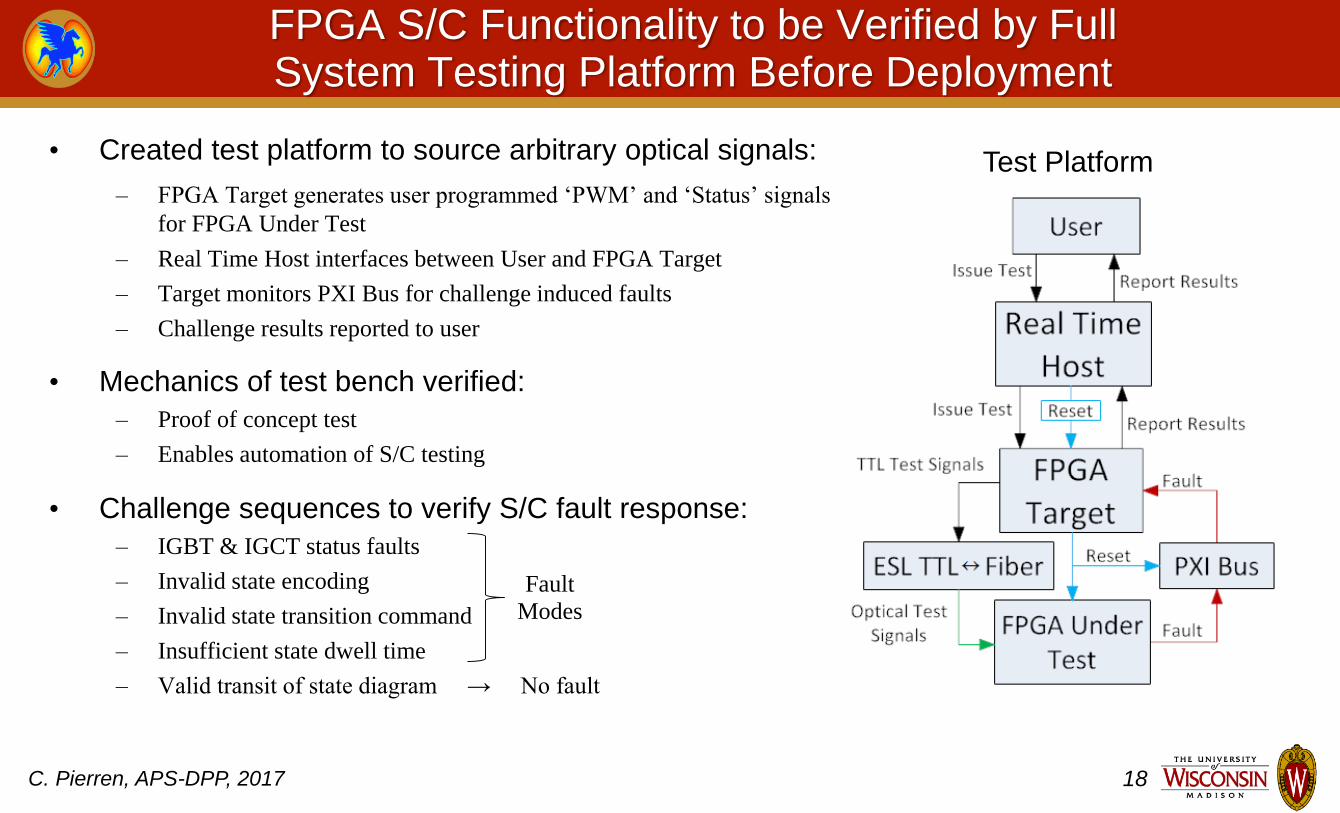
FPGA S/C Functionality to be Verified by Full System Testing Platform Before Deployment
• Created test platform to source arbitrary optical signals:
– FPGA Target generates user programmed ‘PWM’ and ‘Status’ signals
for FPGA Under Test
– Real Time Host interfaces between User and FPGA Target
– Target monitors PXI Bus for challenge induced faults
– Challenge results reported to user
• Mechanics of test bench verified:
– Proof of concept test
– Enables automation of S/C testing
• Challenge sequences to verify S/C fault response:
– IGBT & IGCT status faults
– Invalid state encoding
– Invalid state transition command
– Insufficient state dwell time
– Valid transit of state diagram → No fault
Fault
Modes
C. Pierren, APS-DPP, 2017
Test Platform

19
Development & Deployment Plan for Power Supply & Control System Upgrades
• FPGA Splitter/Combiner
– Expands control channels; TF upgrade
– IGCT protection
• Ćuk converter for injector Arc and Bias supplies
– Low ripple voltage control
• FPGA digital PWM
– Programmable coil & LHI control
– Advanced control algorithms
C. Pierren, APS-DPP, 2017
Near-Term Proposed
• DNB power supply & control
• RF/EBW power supply & control
• FPGA replacement of CAMAC timing modules

20
Physics Studies Enabled by Planned & Proposed Upgrades
• Helicity Injection Control:
– Helicity drive scans
– Potential for tandem operation of low-field
and high-field side helicity injection
• Increased TF:
– Explore higher TF operating space relevant
to start-up on larger machines
– Increased Taylor limit studies
• PF Expansion:
– Improved vertical position control
– Better coupling to helicity injectors
• OH Operations:
– Impurity studies
– Taylor limit studies
– LHI to OH handoff
• DNB Control:
– Plasma kinetic & impurity measurements
–
• RF/EBW Control:
– Electron heating
– Current drive
C. Pierren, APS-DPP, 2017

21
Summary: FPGA Technology Applied to Pegasus & Pegasus-E
• FPGAs improve control and support expansion of Pegasus power supply
– Commercial off-the-shelf hardware and software
• FPGA S/C system designed as first application
– Protects all power supplies and enables expansion
– Improves fault response and monitoring
– Improves device-level protections
• Hardware & design verification in progress prior to powered testing
• Next steps:
– Ćuk power supplies: Injector Arc & Bias
– FPGA Digital Control
– DNB, RF/EBW power supply
C. Pierren, APS-DPP, 2017

Pegasus Power Systems

FPGA Hardware Provides Flexible Control

FPGA Splitter-Combiner Design

Hardware & Software Verification

Planned Upgrades to Control System & Power Supplies
27
Reprints
Reprints of this and other PEGASUS presentations are available online at
http://pegasus.ep.wisc.edu/Technical_Reports