enhancing hole mobility in iii-v semiconductors hole mobility in iii-v semiconductors ... note that...
TRANSCRIPT

Enhancing hole mobility in III-V semiconductors
Aneesh Nainani,1,a) Brian R. Bennett,2 J. Brad Boos,2 Mario G. Ancona,2
and Krishna C. Saraswat11Department of Electrical Engineering, Center for Integrated Systems, Stanford University, Stanford,California 94305, USA2Naval Research Laboratory, Washington, DC 20375, USA
(Received 17 November 2011; accepted 16 April 2012; published online 21 May 2012)
Transistors based on III-V semiconductor materials have been used for a variety of analog and high
frequency applications driven by the high electron mobilities in III-V materials. On the other hand,
the hole mobility in III-V materials has always lagged compared to group-IV semiconductors such
as germanium. In this paper, we explore the use of strain and heterostructure design guided by
bandstructure modeling to enhance the hole mobility in III-V materials. Parameters such as strain,
valence band offset, effective masses, and splitting between the light and heavy hole bands that are
important for optimizing hole transport are measured quantitatively using various experimental
techniques. A peak Hall mobility for the holes of 960 cm2/Vs is demonstrated and the high
hole mobility is maintained even at high sheet charge. VC 2012 American Institute of Physics.[http://dx.doi.org/10.1063/1.4718381]
I. INTRODUCTION
III-V semiconductors have been used extensively for
making high electron mobility transistors (HEMTs) and het-
erojunction bipolar transistors (HBTs) for analog, digital,
and mixed-signal high-frequency applications. Recently,
with the development of high quality dielectrics on III-V
surfaces, III-V materials are also being actively investigated
for replacing silicon as the channel material for making
MOSFETs for low power/high performance applications.1–3
Most of these developments have been driven by the promise
of higher electron mobilities and the potential benefits of het-
erostructure engineering with nearly lattice-matched semi-
conductors.4 For p-channel devices, the advantages have
been less clear because the hole mobility in III-V materials
has always lagged compared to group-IV semiconductors
such as silicon and germanium. In particular, this has been a
limiting factor for reducing base resistance in the p-type base
of a III-V HBT and for obtaining a high performance channel
for a III-V p-channel field-effect transistor (FET).
In the case of silicon, the hole mobility has been greatly
enhanced through the use of strain. Up to two times enhance-
ment in hole mobility and drive current is obtained in state-
of-the-art p-channel silicon transistors using uniaxial strain.5
Theoretical calculations have predicted greater than four
times enhancement in the future.5 III-V systems offer great
flexibility for strain engineering via control of the lattice
mismatch between the channel and the underlying layers.
Furthermore, heterostructure design of III-V transistors can
be used to create a quantum well channel for the holes that
can be used to further improve the hole transport. Given the
latitude III-V materials offer in material options and strain
configurations, a useful first step is to use modeling to help
engineer the stack and strain for optimum hole transport.
In 1983, Osbourn6 proposed the use of a strained
InxGa1�xAs layer to enhance the hole mobility and thereby
improve the performance of a p-channel FET. Laikhtman
et al.7 presented a modeling study of the InGaAs/AlGaAs
system with the objective of discussing the critical parame-
ters influencing hole transport. More recently, Bennett et al.demonstrated the use of biaxial strain in InxGa1�xSb (Ref. 8)
and GaSb (Ref. 9) channels to enhance the hole mobility and
obtained hole mobilities of greater than 1000 cm2/Vs at a
sheet charge of 1� 1012/cm2.10 The key concept behind
these schemes for enhancing hole mobility is demonstrated
in Figure 1, where a narrow bandgap material is inserted
between the wide bandgap layers creating a quantum well for
the confined holes. The amount of strain present in the narrow
bandgap channel can be varied by engineering the lattice mis-
match between the channel and barrier layers. The presence of
strain and confinement splits the degeneracy between the light
hole (lh) and heavy hole (hh) bands (Figure 1). This improves
mobility both by increasing the occupancy of carriers in the
light hole band that has a lower transport effective mass and
by reducing the number of final states available for interband
scattering of the holes. Note that we are labeling the lowest
occupied hole band as the light hole band (Figure 1) which is
indeed the band with lighter hole effective mass in our case as
discussed later.
The important parameters for designing the quantum
well (Figure 1) to enhance hole mobility are the percentage
of strain induced in the channel, the valence band offset
(VBO) between the narrow bandgap channel and the wide
bandgap buffer which determines the maximum number of
holes confined in the quantum well, the number and effective
mass (m*) of the carriers in the light hole (lh) and heavy
hole (hh) bands, and the energy split between the lh and hhbands (Dlh-hh). Also it is important to identify the dominant
scattering mechanism, which limits the mobility of this two-
dimensional hole gas (2DHG).a)email: [email protected].
0021-8979/2012/111(10)/103706/12/$30.00 VC 2012 American Institute of Physics111, 103706-1
JOURNAL OF APPLIED PHYSICS 111, 103706 (2012)
Downloaded 21 May 2012 to 132.250.22.5. Redistribution subject to AIP license or copyright; see http://jap.aip.org/about/rights_and_permissions

In this paper, we first used 8 band k.p bandstructure cal-
culations to identify the optimum channel and strain configu-
ration for high hole mobility in III-V semiconductors. Based
on the insight gained from the modeling, two different heter-
ostructure designs with strained antimony (Sb) based chan-
nels were fabricated and analyzed. The amount of strain
present in the channel was quantified using x-ray diffraction
(XRD) analysis. X-ray photoemission spectroscopy (XPS)
analysis was used to estimate the valence band offset.
Temperature-dependent Hall measurements were performed
to identify the dominant scattering mechanisms, and mobility
spectrum analysis (MSA) was used to estimate the number
of carriers in the light and heavy hole bands. Effective mass
and the splitting between the light and heavy hole bands
were quantified using Shubninov-de Haas oscillations
observed in these 2DHG at low temperatures and high mag-
netic field. Finally, using gated Hall measurements, the hole
mobility was measured as a function of the sheet charge in
InxGa1�xSb channels optimized for hole transport. A hole
mobility of 960 cm2/Vs at a sheet charge of 1� 1012/cm2
was measured. The mobility remained more than 3 times
higher in comparison with uniaxially strained silicon even at
a high sheet charge of 7� 1012/cm2.
The rest of the paper is organized as follows. In Sec. II,
we present modeling analysis to predict the optimum mate-
rial and strain configuration for obtaining high hole mobility.
Section III discusses the two heterostructure designs that
were fabricated and analyzed for hole transport. Section IV
details the experiments that were performed on these stacks
to measure the amount of strain, the effective masses, the
splitting of the light and heavy hole bands, the valence band
offset, and the identification of the dominant scattering
mechanism. Section V reports on gated Hall bar measure-
ments and mobility results. Finally, the conclusions are sum-
marized in Sec. VI. These results demonstrate that high hole
mobility can be obtained in III-V materials with prudent ma-
terial selection and optimum strain and heterostructure
design. This will serve as an important step in the develop-
ment of high performance III-V pMOSFET’s and III-V npn
HBT’s. The process of material selection and device design
guided by modeling and direct measurement of quantum me-
chanical parameters that determined the transport can be
applied to other material systems as well and should be use-
ful for a broader audience.
II. MODELING
As done in Ref. 11, we used an 8 band k.p approach to
model the bandstructure for technologically relevant arsenic
(As) and antimony (Sb) based III-V compounds. An 8 � 8
Hamiltonian11 with spin orbit coupling was used to evaluate
strain effects under both biaxial and uniaxial conditions. Pa-
rameters used for the simulation were calibrated against the
bulk bandstructure obtained using the non-local empirical
pseudopotential method with and without strain. A self-
consistent method was used to calculate the valence subband
structure.12 The use of the 8 band model,13 which includes
the interaction between the conduction, light, heavy, and
split-off hole bands, matches the results from an empirical
pseudopotential method better than the 6-band k.p model14
which only accounts for coupling between the light, heavy,
and split-off bands. This coupling of the conduction band
with valence bands is especially important for low bandgap
III-V materials such as InAs and InSb. Bandstructures of ter-
tiary InxGa1�xAs and InxGa1�xSb were calculated using the
band parameters of binary end points using Bowdin’s
interpolation.15
Figure 2 plots the isoenergy surfaces of the upper va-
lence band at 2, 25 and 50meV for silicon, GaAs and InSb.
We observe that for GaAs and InSb, the valence-band isoe-
nergy surface remains relatively isotropic with increasing
energy as compared to silicon. In the case of silicon, the va-
lence bands are warped to start with and the warping reflec-
tive of the non-parabolicity increases with increasing energy
(Figure 2). Figure 3 shows the isoenergy surfaces for the
upper valence band of GaAs with biaxial and uniaxial-[110]
compressions. For biaxial stress, the energy surface is an
ellipsoid with the energy contours in the x-y plane being
circles (Figure 3(a)); the band is lh-like in the plane of the
stress and hh-like out-of-plane. Under uniaxial compression
FIG. 1. VBO, amount of strain, effective mass (m*) and splitting (Dlh-hh)
between the light hole (lh) and heavy hole (hh) offsets are important parame-
ters for obtaining high hole mobility in III-V heterostructures.
FIG. 2. Isoenergy surfaces for upper valence band in silicon, GaAs and
InSb at 2meV/25meV/50meV.
103706-2 Nainani et al. J. Appl. Phys. 111, 103706 (2012)
Downloaded 21 May 2012 to 132.250.22.5. Redistribution subject to AIP license or copyright; see http://jap.aip.org/about/rights_and_permissions

(along [110]), the energy contour for the top band in the x-y
plane (Figure 3(b)) is an ellipse with the major axis along
[-110] and the minor axis along [110]. Though qualitatively
the effect of strain on III-V materials is similar to group-IV
elements, the prime differences arise from: (a) the initial iso-
tropy of the valence bands in III-V’s as compared to Si/Ge
(Figure 2), (b) the lower modulus of elasticity resulting in
more strain for the same amount of stress in III-V’s as com-
pared to Si/Ge (Table I), and (c) the additional effect due
to increased mixing with the conduction band especially for
III-V’s with low-bandgap.
Table I lists the low field hole mobility for various III-V
binaries. It is well known that for electrons in III-V semicon-
ductors, polar scattering is the dominant scattering mecha-
nism as non-polar optical phonons do not interact with the
electrons due to the s-like spherical symmetry of the conduc-
tion band in III-V’s.16 In the case of holes, however, both de-
formation potential and polar scattering mechanisms are
important for mobility calculations. In Table I, we observe
that varying the group III element while keeping the group V
element the same (i.e., InAs ! GaAs) does not change the
hole mobility appreciably while a large change in hole mo-
bility is observed when the group V element is varied (i.e.,
InP ! InAs ! InSb). This is a consequence of the fact that
the valence bands in III-V materials primarily derive from
the p-orbitals of the anion.17 Figure 4 plots the low field hole
mobility of InxGa1�xAs and InxGa1�xSb at a sheet charge
density of 1� 1012/cm2. We accounted for the acoustic/opti-
cal deformation potential and the alloy and polar scattering
mechanisms to calculate the hole mobility.12,13 We observe
that the hole mobility for the ternary III-Vs roughly stays in
between those of the binary end points. Thus, the antimo-
nides have significantly higher hole mobilities than the
arsenides. Note that at higher fields the mobility of the terna-
ries is expected to be less than that of the end point binaries
due to increased alloy scattering.
Next, we study the effectiveness of strain in enhancing
the hole mobility in III-V semiconductors. Figure 5 plots the
hole mobility enhancement for (001) substrate orientation
and a fixed 2% strain. The figure is in the form of a polar
plot where the distance from the origin represents the
enhancement in mobility and the direction represents the
channel direction.18 Figure 5(a) plots the enhancement for
2% biaxial compression/tension, while Figure 5(b) is for
fixed 2% uniaxial compression/tension with the uniaxial
strain always applied along the channel direction. Results for
compression/tension are represented with solid/hollow
circles, respectively. We make the following observations:
(a) compressive strain is always better than tensile strain for
hole mobility enhancement in III-V’s. (b) Enhancement with
biaxial strain is approximately isotropic while the strain
response with uniaxial strain has a large directional depend-
ence with the [011] channel direction being optimal. This
can be related to Figure 3 where the isoenergy surface is iso-
tropic in the transport plane for biaxial strain while highly
anisotropic for uniaxial strain. (c) We can get up to 4.3 and
2.3 times enhancement with 2% uniaxial and biaxial
FIG. 3. Isoenergy surface (left) and 2D energy contour along the transport
plane (right) for upper valence band in GaAs for (a) biaxial compression and
(b) uniaxial compression.
TABLE I. Relevant properties of different semiconductor materials at
300K. Note that III-V’s (antimonides in particular) have lower elasticity
constants than silicon.
Eg (eV) mlh mhh
Bulk Mod.
(dyn/cm2)
lh(cm2/Vs)
GaP 2.26 0.14mo 0.79mo 8.8 � 1011 150
GaAs 1.42 0.08mo 0.51mo 7.1 � 1011 400
GaSb 0.72 0.05mo 0.4mo 5.63 � 1011 800
InP 1.34 0.09mo 0.6mo 8.8 � 1011 200
InAs 0.35 0.03mo 0.41mo 5.8 � 1011 450
InSb 0.17 0.02mo 0.43mo 4.7 � 1011 850
Si 1.1 0.17mo 0.49mo 9.9 � 1011 450
Ge 0.67 0.043 mo 0.33 mo 7.5 � 1011 1600
FIG. 4. Calculated hole mobility for varying stoichiometries in InxGa1�xAs
and InxGa1�xSb. Antimonides have twice as high hole mobility compared to
arsenides.
103706-3 Nainani et al. J. Appl. Phys. 111, 103706 (2012)
Downloaded 21 May 2012 to 132.250.22.5. Redistribution subject to AIP license or copyright; see http://jap.aip.org/about/rights_and_permissions
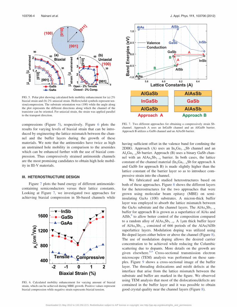
compressions (Figure 5), respectively. Figure 6 plots the
results for varying levels of biaxial strain that can be intro-
duced by engineering the lattice mismatch between the chan-
nel and the buffer layers during the growth of these
materials. We note that the antimonides have twice as high
an unstrained hole mobility in comparison to the arsenides
which can be enhanced further with the use of biaxial com-
pression. Thus compressively strained antimonide channels
are the most promising candidates to obtain high hole mobil-
ity in III-V materials.
III. HETEROSTRUCTURE DESIGN
Figure 7 plots the band energy of different antimonide-
containing semiconductors versus their lattice constants.
Looking at Figure 7, we investigated two approaches for
achieving biaxial compression in Sb-based channels while
having sufficient offset in the valence band for confining the
2DHG. Approach (A) uses an InxGa1�xSb channel and an
AlyGa1�ySb barrier. Approach (B) uses a binary GaSb chan-
nel with an AlAsxSb1�x barrier. In both cases, the lattice
constant of the channel material (InxGa1�xSb for approach A
and GaSb for approach B) is made slightly higher than the
lattice constant of the barrier layer so as to introduce com-
pressive strain into the channel.
We fabricated and studied heterostructures based on
both of these approaches. Figure 8 shows the different layers
for the heterostructures for the two approaches that were
grown using molecular beam epitaxy (MBE) on semi-
insulating GaAs (100) substrates. A micron-thick buffer
layer was employed to absorb the lattice mismatch between
the GaAs substrate and the channel layers. The AlAsxSb1�x
buffer for approach B is grown as a superlattice of AlAs and
AlSb,9 to allow better control of the composition compared
to a random alloy of AlAsxSb1�x. A 1lm thick buffer layer
of AlAsxSb1�x consisted of 666 periods of the AlAs/AlSb
superlattice layers. Modulation doping was utilized using
Be-doped layers either below or above the channel (Figure 8).
The use of modulation doping allows the desired carrier
concentration to be achieved while reducing the Columbic
scattering due to dopants. More details on the growth are
given elsewhere.8,9 Cross-sectional transmission electron
microscope (TEM) analysis was performed on these sam-
ples. Figure 9 shows a cross-sectional image of the buffer
layer. The threading dislocations and misfit defects at the
interface that arise from the lattice mismatch between the
substrate and buffer are marked in the figure. We observed
using TEM analysis that most of the dislocations/defects are
contained in the buffer layer and it was possible to obtain
good crystal quality near the channel layers (Figure 8).
-2 -1 0 1 2400
800
1200
1600
Compressive Tensile
Biaxial Strain (%)
μμ μμ h(cm
2 /Vs)
GaAs
InSbGaSb
FIG. 6. Calculated mobility enhancement for varying amount of biaxial
strain, which can be achieved during MBE growth. Positive values represent
biaxial compression while negative strain represents biaxial tension.
5.8 6.0 6.2 6.4-1.0
-0.5
0.0
0.5
1.0
B
B
A
Ban
d En
ergi
es (e
V)
AlAs
InSb
AlSb
GaSb
GaSb
AlAs
AlSb
o
o
o
o
o
o
o
Valence Conduction
oInSb
Lattice Constants (A)
A
AlAsSb
AlAsSbGaSb
AlGaSb
AlGaSbInGaSb
Approach A Approach B
FIG. 7. Two different approaches for obtaining a compressively strain Sb-
channel. Approach A uses an InGaSb channel and an AlGaSb barrier.
Approach B utilizes a GaSb channel and an AlAsSb barrier.
FIG. 5. Polar plot showing calculated hole mobility enhancement for (a) 2%
biaxial strain and (b) 2% uniaxial strain. Hollow/solid symbols represent ten-
sion/compression. The substrate orientation was (100) while the angle along
the plot represents the different directions along which the channel of the
transistor can be oriented. For uniaxial strain, the strain was applied parallel
to the transport direction.
103706-4 Nainani et al. J. Appl. Phys. 111, 103706 (2012)
Downloaded 21 May 2012 to 132.250.22.5. Redistribution subject to AIP license or copyright; see http://jap.aip.org/about/rights_and_permissions

IV. EXPERIMENTS
In this section, we present various experiments con-
ducted on the heterostructures discussed in Sec. III to quan-
tify the amount of strain present in the channel, the VBO, the
effective masses and the number of carriers in the light and
heavy hole bands, splitting between the light/heavy bands,
and the mobility. Table II outlines the experiments per-
formed and the corresponding figures. The different samples
studied are listed in Table III.
A. Strain
Compressive strain was introduced intentionally in the
channel of our stacks to enhance the hole mobility. We used
high resolution XRD analysis to quantify the strain present in
the channel and also to check for any residual strain present in
the metamorphic buffer as it absorbs the lattice mismatch with
the GaAs substrate. Figure 10 shows the rocking curves near
the (004) GaAs peak for sample A1 (with In0.41Ga0.59Sb chan-
nel) and sample B1 (GaSb channel with superlattice of
(AlAs)x(AlSb)1�x). The different peaks in the rocking curve
for sample A1 (Figure 10(a)) correspond to the peak from the
GaAs substrate, the metamorphic AlGaSb buffer and the peak
from the InGaSb channel. For sample B1, we see the main
and satellite peaks from the (AlAs)xAlSb1�x which are char-
acteristics of the digital superlattice (n¼�1,0, andþ 1) that
was used in the metamorphic buffer. The GaSb channel peak
gets buried in the n¼ 0 satellite peak from the superlattice.
The thicknesses for the AlSb and AlAs layers are determined
by matching the experimental results with simulations and the
AlAsxSb1�x ternary composition is calculated using Vegard’s
law. Table III summarizes the results. Reciprocal lattice scans
were performed on a few samples to further quantify the strain
present and to check for the presence of residual strain in the
metamorphic buffer layer. Figure 11 plots the scan around the
(004) and (115) reciprocal lattice points. The peaks from the
metamorphic buffer showed that the buffer was 97% relaxed
and the channel was pseudomorphically strained with respect
to the buffer layer. The epilayer peaks were broadened as a
result of a high density of misfit dislocations generated by the
large 7%-8% lattice mismatch with the substrate.
FIG. 8. Cross-section showing the different layers in a quantum-well hetero-
structure with (a) InxGa1�xSb and (b) GaSb channel. The AlAsxSb1�x layer
is composed of a AlSb/AlAs short-period superlattice. Also shown are high
resolution TEM images around the channel region.
FIG. 9. (a) Dislocations and (b) misfit defects in the buffer layer which
accommodates the large lattice mismatch between the channel and the GaAs
substrate.
TABLE II. Parameters measured, technique used, and corresponding
figures.
Property measured Technique used Corresponding figures
Crystal quality HR-TEM 8 and 9
Strain HR-XRD 10 and 11
VBO XPS 12 and 13
Transport analysis Hall measurements 14 and 15
Number of holes in lh/hh bands MSA 16 and 17
Effective mass SdH 18
Dlh-hh SdH 19 and 20
Mobility Gated Hall 21
103706-5 Nainani et al. J. Appl. Phys. 111, 103706 (2012)
Downloaded 21 May 2012 to 132.250.22.5. Redistribution subject to AIP license or copyright; see http://jap.aip.org/about/rights_and_permissions

B. Valence band offset measurement
A significant VBO is needed in order to confine the
2DHG in the channel layer. An experimental measurement
of the offset is important as it might be affected by the quan-
tization and strain in the narrow quantum well channel. We
used low energy XPS analysis which is the most accurate
method to measure the valence band offset.19 A timed etch
was used to etch various layers in the heterostructure shown
in Figure 8. VBO was calculated by taking the difference
between the valence band spectrum from the channel and
barrier layers (Figures 12 and 13). The signal from the chan-
nel versus the buffer layer is differentiated by monitoring the
element that is different between the channel and buffer
layer, i.e., indium in the InGaSb/AlGaSb stack in approach
A (Figure 12) and gallium in the GaSb/AlAsySb1�y channel
in approach B (Figure 13). The valence band offset is esti-
mated to be �0.3 eV for sample A1 (Figure 12) and 0.6 eV
for sample B1 (Figure 13). Approximately twice as high a
VBO is achieved using the AlAsxSb1�x barrier (approach B)
as compared to AlyGa1�ySb barrier (approach A), which was
also expected from the bulk band lineup in Figure 7. Both
band offsets are sufficient to confine the 2DHG and are com-
parable or higher than the corresponding numbers in the
Si1�xGex/Si system.20,21
C. Transport measurements
Since the 2DHG in our structures is confined in a
strained quantum well, it is important to quantify the mobil-
ity in our samples and identify the scattering mechanisms
that are limiting the mobility. It is especially important to
check whether the mobility is limited by phonon-related
effects that are inherent to the semiconductor, or by scatter-
ing at the interface. Fortunately, the interface and phonon
related scattering mechanisms have different temperature
dependences, thus allowing them to be distinguished.
Temperature-dependent Hall measurements were performed
on the samples with the temperature varying from 2K-
300K. Van der Pauw and gated Hall bar structures were fab-
ricated for the measurements which were performed by an
automated setup with a magnetic field range of 0-9 T. The
TABLE III. Details on the samples studied. Mobility and sheet charge (NS) at 300K measured using Hall measurements are listed along with value of light
hole effective mass measured using Shubnikov–de Haas oscillations.
Samples Channel (Thickness (A)) Barrier Strain (%) lHall (300K)(cm2 V�1 s�1) NS (cm
�2) m* (m0)
A1 In0.41Ga0.59Sb (75 A) Al0.7Ga0.3Sb 1.8 960 1.3 � 1012 0.099
A2 In0.41Ga0.59Sb (75 A) AlSb 1.9 900 0.94 � 1012 0.094
A3 In0.41Ga0.59Sb(125 A) Al0.7Ga0.3Sb 1.8 a 621 1.0 � 1012 Strain relaxation: No oscillations
B1 GaSb (75 A) AlAs0.219Sb0.781 1.06 880 1.5 � 1012 0.12
B2 GaSb (75 A) AlAs0.238Sb0.762 1.48a 600 1.27 � 1012 Strain relaxation: No oscillations
aFor samples A3 and B2, the ideally targeted value of strain is listed. Mobility degradation is observed due to strain relaxation in these samples due to channel
width exceeding the critical layer thickness.
FIG. 10. High Resolution XRD scans on the samples
A1 (top) and B1 (bottom) near the (004) GaAs peak.
For sample B1, which uses (AlAs)AlSb as the buffer,
we observe main and satellite peaks characteristic of
the digital superlattice.
103706-6 Nainani et al. J. Appl. Phys. 111, 103706 (2012)
Downloaded 21 May 2012 to 132.250.22.5. Redistribution subject to AIP license or copyright; see http://jap.aip.org/about/rights_and_permissions

temperature range of the measurements is limited by system
configuration.
Figure 14 plots the hole mobility (lh) and and sheet
charge (NS) values obtained from these measurements. For
samples A1, A2, and B1, a T�3/2 temperature dependence of
hole mobility, characteristic of a mobility limited by phonon
scattering, is seen in the temperature range of 150-
300K.16,22 Also the sheet charge remains nearly constant as
a function of temperature in these samples as expected from
their use of modulation doping. For samples A3 and B2,
strain relaxation occurs due to either the channel thickness
exceeding the critical limit (A3) or the lattice mismatch
exceeding the maximum possible at that particular thickness
(B2). We observe that the temperature dependence weakens
to T�1, an effect that suggests a mobility limited by interface
defects.16 Also there is a significant drop in the low tempera-
ture mobility in these samples, which is more sensitive to
interface quality. Samples A3 and B2 also exhibit a slight
freeze out of sheet charge at low temperature, again suggest-
ing a poor interface and/or the presence of dislocations as a
result of strain relaxation in these samples. Thus, it appears
the room temperature mobility in our samples is limited by
phonon-based scattering mechanisms when the strain in con-
fined in the channel, and limited by interface-related scatter-
ing when there is a relaxation of the strain. We measured a
maximum hole mobility of 960 cm2/Vs at a sheet charge of
�1� 1012 cm2/Vs. To further confirm our interpretation, a
FIG. 11. Reciprocal lattice scan on sample B1 around GaAs (004)
and (115).
FIG. 12. VBO for sample A1 (approach A) is calculated by taking the difference
in the valence band spectrum from the InxGa1�xSb channel and AlyGa1�ySb
buffer.
FIG. 13. VBO for sample B1 (approach B) is calculated by taking the differ-
ence in the valence band spectrum from the GaSb channel and the
AlAsySb1�y buffer.
103706-7 Nainani et al. J. Appl. Phys. 111, 103706 (2012)
Downloaded 21 May 2012 to 132.250.22.5. Redistribution subject to AIP license or copyright; see http://jap.aip.org/about/rights_and_permissions

high temperature anneal (600 �C/60 s) was performed on one
of the samples during MBE just before the channel growth.
This is expected to improve the quality of the channel/barrier
interface, and indeed we observed a higher low-temperature
hole mobility (Figure 15), but only a slight increase in the
hole mobility at room temperature, which again is limited by
phonon scattering.
D. Mobility spectrum analysis
Mobility spectrum analysis is a valuable technique that
allows one to check for parallel conduction in a heterostruc-
ture with different layers and to quantify the number of car-
rier in each band.23 In this technique, the magnetic field is
varied from 0-9 T to check for the presence of multiple con-
ductive channels. The Hall coefficient and the resistivity are
measured as a function of the varying magnetic field for vari-
ous temperatures. The conductivity tensors rxx and rxy can
be extracted from the measured Hall coefficient (RH) and re-
sistivity using the equations below24
Ex ¼ qxx Jx; (1)
qxx ¼ryy
rxxryy þ r2xy; qxy ¼ � rxy
rxxryy þ r2xy; (2)
Ey ¼ qyx Jx ¼ RHBJx; RH ¼ qyxB
¼ rxyrxxryy þ r2xy
1
B: (3)
The components of the conductivity tensor are related to the
charge and mobility of individual carriers in a N-carrier sys-
tem as
rxx ¼XN1
niqili1þ l2i B
2; rxy ¼
XN1
niqil2i B1þ l2i B
2: (4)
where ni and li are the sheet charge and mobility corre-
sponding to the ith carrier, respectively. Figures 16(a) and
16(b) plot the components of the conductivity tensor as a
function of the magnetic field measured at many tempera-
tures. A least squares algorithm is used to fit the experimen-
tal data assuming one, two, and three types of carriers as per
Eq. (4). We find that the fit to the experimentally measured
conductivity tensors (Figure 16) is excellent when we
assume that only the lh and hh bands are occupied, thus
FIG. 14. Hole mobility (lh) and sheet charge (Ns) are measured as a function of temperature using Hall measurements for samples: A1, A2, A3 (top) and B1,
B2 (bottom).
103706-8 Nainani et al. J. Appl. Phys. 111, 103706 (2012)
Downloaded 21 May 2012 to 132.250.22.5. Redistribution subject to AIP license or copyright; see http://jap.aip.org/about/rights_and_permissions

ruling out any parallel conduction in the heterostructure
stack. The number and mobility of the carriers in the lh and
hh bands were calculated as per Eq. (4) and plotted in Figure
17 for different temperatures. We observe for sample A1
(with a sheet charge of �1 � 1012/cm2) that only the lh band
is occupied at 2K (Figure 17), that the hh band starts to
become occupied as the temperature increases, and that the
number of carriers in lh and hh bands becomes comparable
at room temperature.
E. Effective mass and the splitting between the light/heavy hole bands
Shubnikov-de-Haas (SdH) oscillations were observed in
our samples at low temperature (2-20K) and high magnetic
fields (0-9 T). Figure 18 (inset) plots the scan of sheet resist-
ance with magnetic field for sample A1 with a mobility of
4500 cm2/Vs and a sheet charge of 1.3 � 1012/cm2 at 2K.
An oscillatory behavior can clearly be seen superimposed on
a parabolic dependence with magnetic field. The oscillatory
behavior is plotted versus magnetic field in Figure 18 for var-
ious temperatures, with the parabolic dependence due to
hole-hole interactions25 removed. It is well known that these
oscillations occur only when there is a low density of defects
in the bulk of the channel or at its interfaces; hence observa-
tion of SdH oscillations provides more evidence of the good
crystal quality in the channel and at the interfaces. Moreover,
no oscillations were observed in the samples A3 and B2
where relaxation of strain occurred leading presumably to a
deterioration of interface quality.
Besides confirming good crystal quality, significant
quantitative information such as the effective masses of car-
riers in the light and heavy hole bands (m*) and the splitting
between the light and heavy hole bands (Dlh-hh) can be
extracted from SdH oscillations. Figure 19 plots the oscilla-
tory behavior at 2K versus the inverse of the magnetic field
(1/B) at a sheet charge of 1.1� 1012/cm2. The oscillations
appear periodic in nature and a fast Fourier transform (FFT)
of the data shows that the oscillations are harmonic with a
single frequency (Figure 19 (inset)) implying occupancy of
only the lowest energy light-hole subband at this sheet
charge density. The effective mass of the light hole band is
calculated from the temperature dependence of the SdH
oscillations. The peak amplitude of the oscillations (Dqp)can be described using the Ando formula26 as
Dqq0
¼ RsVn
sinhnexp
�pxcsq
� �; (5)
where q0 is the resistance at zero B, sq is the quantum life-
time, n ¼ 2p2kT=xc and xc ¼ eB=m�. The prefactor Rs is
associated with Zeeman splitting, while V is usually set
equal to 4. RS and V are assumed to be independent of mag-
netic field and temperature in which case they were not
involved in the following analysis. lnDqpq0
� �is plotted versus
ln nsinh n
� �in the temperature range of 2–10K, for various val-
ues of B at which the peak occurs. mlh* was calculated as the
value for which a gradient of unity is obtained in each sam-
ple. Table III summarizes the mlh* values for the different
samples. The m*lh of 0.094m0 obtained in sample A1 was
FIG. 15. A high temperature anneal (600 �C/60 s) before channel growth to
optimize the interface results in a large increase in low-temperature mobility
but gives only a slight gain (900 cm2/Vs to 940 cm2/Vs) in mobility at
300K.
0 2 4 6 8 90.0
1.0x10⁻⁴
2.0x10⁻⁴
3.0x10⁻⁴
4.0x10⁻⁴
5.0x10⁻⁴
6.0x10⁻⁴
7.0x10⁻⁴
σσ σσ XX(m
ho-s
q)
2K 50K 150K 300K
Experimental Simulated
B (Tesla)
0 2 4 6 8 90.0
1.0x10⁻⁴
2.0x10⁻⁴
3.0x10⁻⁴
4.0x10⁻⁴ Experimental Simulated
σσ σσ XY(m
ho-s
q)
2K 50K 150K 300K
B (Tesla)
(a)
(b)
FIG. 16. Conductivity tensors (rxx and rxx) are measured as a function of
magnetic field (B) for various temperatures. MSA on the data confirms that
there is no parallel conduction in the stack and is used to estimate number of
carriers in lh/hh bands and their mobility (Figure 17).
103706-9 Nainani et al. J. Appl. Phys. 111, 103706 (2012)
Downloaded 21 May 2012 to 132.250.22.5. Redistribution subject to AIP license or copyright; see http://jap.aip.org/about/rights_and_permissions

verified using cyclotron resonance. The presence of strain
and confinement in these samples leads to a reduction of
hole effective mass to 0.094m0, which is close to the value
typically found for the electron effective mass in III-V
materials.
Figure 20 plots the oscillatory behavior on the same sam-
ple at a sheet charge of 3.5� 1012/cm2. We see that now there
are two frequencies beating, and an FFT of the data corre-
spondingly shows two dominant peaks (Figure 20 (inset))
meaning that both the lh and hh bands are occupied at this
sheet charge density. The energy splitting between the lh and
hh bands (Dlh-hh) can be calculated from the onset at which
the second frequency starts to occur and was estimated to be
between 70 and 80meV from sample A1. In the well-studied
case of strain in silicon it is known that the splitting between
the light and heavy hole bands must be more than the energy
of the optical phonon in silicon (60meV) if there is to be
effective suppression of interband scattering between the light
and heavy hole bands.27 The optical phonon energy is
�28meV for GaSb and �30meV for InSb, and thus our
measured energy splitting would seem to be sufficient for sup-
pressing the interband scattering and giving a large enhance-
ment in hole mobility. The effective mass of the carriers in the
heavy hole bands (mhh*) can be calculated from the tempera-
ture dependence of the second oscillation and was found to be
0.36 0.05 m0 for sample A1. The larger uncertainty in the
measurement of the heavy hole mass arises from the superpo-
sition of the two oscillations from the light and heavy hole
bands when both of the bands are occupied making it more
difficult to separate the individual components.
0 50 100 150 200 250 3000
2x10¹¹
4x10¹¹
6x10¹¹
8x10¹¹
1x10¹²
NS (
/cm
2 )
Temp (K)
light hole (lh)heavy hole (hh)
(a)
0 50 100 150 200 250 300102
5x10²
103
5x10³
μμ μμ h(cm
2 /Vs)
light hole (lh)heavy hole (hh)
Temp (K)
(b)
FIG. 17. (a) Number and (b) mobility of carriers in the light (lh) and heavy
hole (hh) bands as a function of temperature for sample A1.
0 1 2 3 4 5 6 7 8 9
-0.3
-0.2
-0.1
0.0
0.1
0.2
0.3
m*=0.0099
2K 4K 6K 8K 10K
Temperature
ΔρΔ ρ ΔρΔ ρXX
/ ρρ ρρxx
B (Tesla)
m*=0.01
0 1 2 3 4 5 6 7 8 91000
1100
1200
1300
1400
1500
1600
1700
Rs ( ΩΩ ΩΩ
/sqa
ure)
T em p = 2K
B (Tesla)
FIG. 18. Shubnikov-de-Haas (SdH) oscillations in sheet resistance (inset)
are observed at low temperatures and high magnetic field. Temperature de-
pendence of these oscillations is used to calculatem* (Table III).
0.1 0.2 0.3 0.4 0.5
-0.3
-0.2
-0.1
0.0
0.1
0.2
ΔρΔρ ΔρΔρXX
/ ρρ ρρxx
1 /B (1/Tesla)
2K, N S = 1.1x10¹²/cm 2
20 40 60 80 100
4.0x10⁻⁴
8.0x10⁻⁴
1.2x10⁻³
1.6x10⁻³FFT
One Frequency =>Only lh Band Occupied
Frequency
lh
hh
FIG. 19. SdH oscillations at 2K are plotted vs. 1/B for a sheet charge of
1.1� 1012/cm2. The oscillatory behavior is periodic in nature with a single
dominant frequency, indicating that only the lh band is occupied at this sheetcharge.
0.1 0.2 0.3 0.4 0.5
-0.2
-0.1
0.0
0.1
ΔρΔρ ΔρΔρXX
/ ρρ ρρxx
1 /B (1/Tesla)
2K , N S = 3.5x10¹²/cm 2
20 40 60 80 100
2.0x10⁻⁵
4.0x10⁻⁵
6.0x10⁻⁵
8.0x10⁻⁵
1.0x10⁻⁴
1.2x10⁻⁴
1.4x10⁻⁴FFT
Two Frequencies => bothlh and hhBands Occupied
Frequency
lh
hh
FIG. 20. SdH oscillations at 2K are plotted vs. 1/B for sheet charge of
3.5� 1012/cm2. The oscillations are combinations of two dominant frequen-
cies, indicating that both lh and hh bands are occupied at this sheet charge.
103706-10 Nainani et al. J. Appl. Phys. 111, 103706 (2012)
Downloaded 21 May 2012 to 132.250.22.5. Redistribution subject to AIP license or copyright; see http://jap.aip.org/about/rights_and_permissions
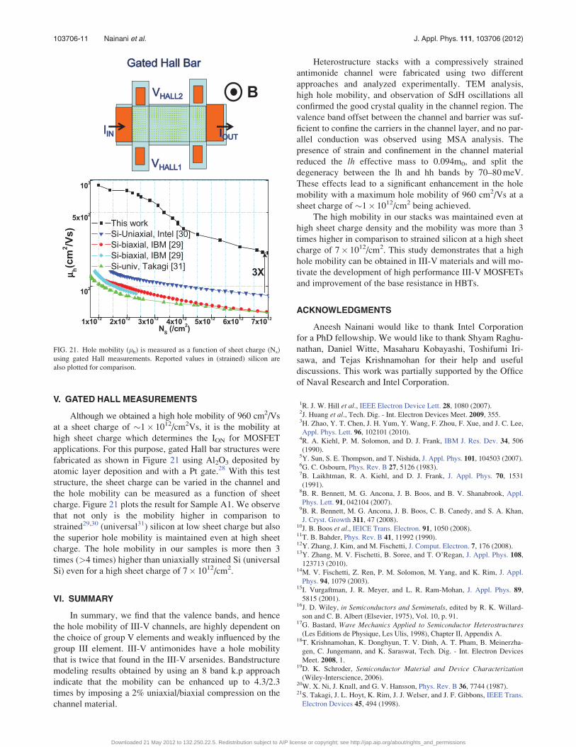
V. GATED HALL MEASUREMENTS
Although we obtained a high hole mobility of 960 cm2/Vs
at a sheet charge of �1� 1012/cm2Vs, it is the mobility at
high sheet charge which determines the ION for MOSFET
applications. For this purpose, gated Hall bar structures were
fabricated as shown in Figure 21 using Al2O3 deposited by
atomic layer deposition and with a Pt gate.28 With this test
structure, the sheet charge can be varied in the channel and
the hole mobility can be measured as a function of sheet
charge. Figure 21 plots the result for Sample A1. We observe
that not only is the mobility higher in comparison to
strained29,30 (universal31) silicon at low sheet charge but also
the superior hole mobility is maintained even at high sheet
charge. The hole mobility in our samples is more then 3
times (>4 times) higher than uniaxially strained Si (universal
Si) even for a high sheet charge of 7� 1012/cm2.
VI. SUMMARY
In summary, we find that the valence bands, and hence
the hole mobility of III-V channels, are highly dependent on
the choice of group V elements and weakly influenced by the
group III element. III-V antimonides have a hole mobility
that is twice that found in the III-V arsenides. Bandstructure
modeling results obtained by using an 8 band k.p approach
indicate that the mobility can be enhanced up to 4.3/2.3
times by imposing a 2% uniaxial/biaxial compression on the
channel material.
Heterostructure stacks with a compressively strained
antimonide channel were fabricated using two different
approaches and analyzed experimentally. TEM analysis,
high hole mobility, and observation of SdH oscillations all
confirmed the good crystal quality in the channel region. The
valence band offset between the channel and barrier was suf-
ficient to confine the carriers in the channel layer, and no par-
allel conduction was observed using MSA analysis. The
presence of strain and confinement in the channel material
reduced the lh effective mass to 0.094m0, and split the
degeneracy between the lh and hh bands by 70–80meV.
These effects lead to a significant enhancement in the hole
mobility with a maximum hole mobility of 960 cm2/Vs at a
sheet charge of �1� 1012/cm2 being achieved.
The high mobility in our stacks was maintained even at
high sheet charge density and the mobility was more than 3
times higher in comparison to strained silicon at a high sheet
charge of 7� 1012/cm2. This study demonstrates that a high
hole mobility can be obtained in III-V materials and will mo-
tivate the development of high performance III-V MOSFETs
and improvement of the base resistance in HBTs.
ACKNOWLEDGMENTS
Aneesh Nainani would like to thank Intel Corporation
for a PhD fellowship. We would like to thank Shyam Raghu-
nathan, Daniel Witte, Masaharu Kobayashi, Toshifumi Iri-
sawa, and Tejas Krishnamohan for their help and useful
discussions. This work was partially supported by the Office
of Naval Research and Intel Corporation.
1R. J. W. Hill et al., IEEE Electron Device Lett. 28, 1080 (2007).2J. Huang et al., Tech. Dig. - Int. Electron Devices Meet. 2009, 355.3H. Zhao, Y. T. Chen, J. H. Yum, Y. Wang, F. Zhou, F. Xue, and J. C. Lee,
Appl. Phys. Lett. 96, 102101 (2010).4R. A. Kiehl, P. M. Solomon, and D. J. Frank, IBM J. Res. Dev. 34, 506(1990).
5Y. Sun, S. E. Thompson, and T. Nishida, J. Appl. Phys. 101, 104503 (2007).6G. C. Osbourn, Phys. Rev. B 27, 5126 (1983).7B. Laikhtman, R. A. Kiehl, and D. J. Frank, J. Appl. Phys. 70, 1531(1991).
8B. R. Bennett, M. G. Ancona, J. B. Boos, and B. V. Shanabrook, Appl.
Phys. Lett. 91, 042104 (2007).9B. R. Bennett, M. G. Ancona, J. B. Boos, C. B. Canedy, and S. A. Khan,
J. Cryst. Growth 311, 47 (2008).10J. B. Boos et al., IEICE Trans. Electron. 91, 1050 (2008).11T. B. Bahder, Phys. Rev. B 41, 11992 (1990).12Y. Zhang, J. Kim, and M. Fischetti, J. Comput. Electron. 7, 176 (2008).13Y. Zhang, M. V. Fischetti, B. Soree, and T. O’Regan, J. Appl. Phys. 108,123713 (2010).
14M. V. Fischetti, Z. Ren, P. M. Solomon, M. Yang, and K. Rim, J. Appl.
Phys. 94, 1079 (2003).15I. Vurgaftman, J. R. Meyer, and L. R. Ram-Mohan, J. Appl. Phys. 89,5815 (2001).
16J. D. Wiley, in Semiconductors and Semimetals, edited by R. K. Willard-
son and C. B. Albert (Elsevier, 1975), Vol. 10, p. 91.17G. Bastard, Wave Mechanics Applied to Semiconductor Heterostructures(Les Editions de Physique, Les Ulis, 1998), Chapter II, Appendix A.
18T. Krishnamohan, K. Donghyun, T. V. Dinh, A. T. Pham, B. Meinerzha-
gen, C. Jungemann, and K. Saraswat, Tech. Dig. - Int. Electron Devices
Meet. 2008, 1.19D. K. Schroder, Semiconductor Material and Device Characterization(Wiley-Interscience, 2006).
20W. X. Ni, J. Knall, and G. V. Hansson, Phys. Rev. B 36, 7744 (1987).21S. Takagi, J. L. Hoyt, K. Rim, J. J. Welser, and J. F. Gibbons, IEEE Trans.
Electron Devices 45, 494 (1998).
1x10¹² 2x10¹² 3x10¹² 4x10¹² 5x10¹² 6x10¹² 7x10¹²
102
5x10²
103
This work Si-Uniaxial, Intel [30]Si-biaxial, IBM [29]Si-biaxial, IBM [29]Si-univ, Takagi [31]
μμ μμ h(cm
2 /Vs)
NS (/cm2)
3X
B
FIG. 21. Hole mobility (lh) is measured as a function of sheet charge (Ns)
using gated Hall measurements. Reported values in (strained) silicon are
also plotted for comparison.
103706-11 Nainani et al. J. Appl. Phys. 111, 103706 (2012)
Downloaded 21 May 2012 to 132.250.22.5. Redistribution subject to AIP license or copyright; see http://jap.aip.org/about/rights_and_permissions

22B. Laikhtman, Appl. Phys. Lett. 59, 3021 (1991).23J. R. Meyer, C. A. Hoffman, J. Antoszewski, and L. Faraone, J. Appl.
Phys. 81, 709 (1997).24N. Miura, Physics of Semiconductors in High Magnetic Fields (Oxford
University Press, USA, 2008).25A. Nainani, T. Irisawa, B. R. Bennett, J. B. Boos, M. G. Ancona, and K. C.
Saraswat, Solid-State Electron. 62, 138 (2011).
26T. Ando, A. B. Fowler, and F. Stern, Rev. Mod. Phys. 54, 437 (1982).27N. Mohta and S. E. Thompson, IEEE Circuits Devices Mag. 21, 18 (2005).28A. Nainani et al., J. Appl. Phys. 109, 114908 (2011).29K. Rim et al., Dig. Tech. Pap. – Symp. VLSI Technol. 2002, 98.30S. Thompson et al., Tech. Dig. - Int. Electron Devices Meet. 2002, 61.31S. Takagi, M. Iwase, and A. Toriumi, Tech. Dig. - Int. Electron Devices
Meet. 1988, 398.
103706-12 Nainani et al. J. Appl. Phys. 111, 103706 (2012)
Downloaded 21 May 2012 to 132.250.22.5. Redistribution subject to AIP license or copyright; see http://jap.aip.org/about/rights_and_permissions