etching gold using oxford ion mill toolsignupmonkey.ece.ucsb.edu/wiki/images/e/e3/44... · ning...
TRANSCRIPT

Ning Cao, Staff Engineer, Nanofab Lab, UCSB
Etching Gold using Oxford Ion Mill Tool
Object: To get the etch rate and selectivity (Al2O3 as an etch mask), as well as etch profile, of Au by using Oxford Ion Mill
tool.
Experimental:
1) Wafer Clean: two 4” Si wafers cleaned by a) soaking in acetone (2’ in ultrasonic bath) and methanol (1’ in ultrasonic
bath), then, DI water rinse; b) dipping them in buffered HF in 1’, then, DI water rinse and nitrogen gas blow dry.
2) Depositing Ti/Au (10/500 nm: nominal thickness) using E-beam#4.
3) Lithography for making the etch pattern:
a) Gasonics: #3 for 3 minutes.
b) Spinning-on HMDS: 3000 rpm for 30 s.
c) Spinning-on SF-8 (PMGI): 1500 rpm for 40 s.
d) Bake at 200 C for 3 minutes.
e) Spinning-on SPR955-0.9: 3000 rpm for 30 s.
f) Bake at 95 C for 90 s.
g) Exposing using Auto-stepper200 for shooting an 11X11 array with 0.38 s (Recipe name: Ning) using the calibration
reticle.
h) Post Exposure bake at 110 C for 90 s.
i) Development in AZ300MIF for 2 minutes.
j) O2 plasma descum 300mT/100W 60 s.
4) Depositing Al2O3 (target thickness: 200 nm, actual thickness: 206 nm, Tooling factor: 149.2) using E-beam#2.

Ning Cao, Staff Engineer, Nanofab Lab, UCSB
5) Lifting-off Al2O3: a) soaking in 1165 striper in 80 C hot-plate for 4h40m; b) soaking in fresh 1165 in 70 C hot-water
ultrasonic wave bath for 5 minutes (ultrasonic wave was on); c) soaking in Isopropanol in room-temperature water
ultrasonic wave bath for 3 minutes (ultrasonic wave was on), then, DI water rinse and nitrogen gas blow dry; d) Gasonics:
recipe: #3 for 3 minutes.
6) Cleaving the wafer into sample pieces for ion-mill.

Ning Cao, Staff Engineer, Nanofab Lab, UCSB
Results:
Table 1. Etch rate and selectivity (Au/Al2O3), and side-wall angle of Au under different ion-mill conditions (both Ar flow
rates to neutralizer and beam are 5 sccm; platen and chamber wall temperatures are 10 and 40 C, respectively; platen
rotation speed is 20 rpm).
Sample# date In (mA) Prf (W) Ib (mA) Vb (V) Va (V)Incident
Angle (o)
Etch Time
(minute)
Etch Rate
(nm/min)
Etch Selectivity
(Au/Al2O3)
Side-wall angle
(o)
Au#1B-00 7/14/2015 65. 8
Au#1B-01 7/14/2015 250 250 50 500 500 -15 15 28.7 13.9 65.9
Au#1B-02 7/14/2015 250 250 150 500 500 -15 3 103.3 12.9 62.6
Au#1B-03 7/14/2015 250 250 150 500 500 -30 3 100 4.5 72.5
Au#1B-04 7/16/2015 250 250 150 500 500 -24.2 3 102.7 5.6 70
Au#1B-05 7/16/2015 250 250 150 500 500 24.2 3 100 5.2 72.3
Au#1B-06 7/22/2015 250 250 150 500 500 0 3.5 114.3 7.9 62.2
Au#1B-07 7/22/2015 250 250 150 500 500 -27.8 3.5 97.7 5.6 72.1
Au#1B-08 7/22/2015 250 250 150 500 500 27.8 3.5 94.6 4.8 76
Au#1B-09 8/25/2015 250 200 50 500 500 -27.8 14 25.6 6.2 72.1
Au#1B-10 8/25/2015 250 200 50 500 500 27.8 14 25.4 4.5 74.6
Au#1B-11 9/11/2015 250 200 100 500 500 27.8 7 56.9 5.1 75.1
Au#1B-12 9/11/2015 250 200 100 500 500 -27.8 7 58.4 6.5 73.5
Au#1B-13 9/16/2015 250 200 150 350 500 27.8 5.5 76.7 4.3 72.5
Au#1B-14 9/16/2015 250 200 150 200 500 27.8 7 49 4.6 70.4
Au#1B-16 9/21/2015 250 250 200 1000 500 -27.8 2.333333333 163 6.4 74.8
Au#1B-17 9/24/2015 250 250 150 1000 500 27.8 3.5 106 5.3 77.9
Au#1B-18 9/24/2015 250 250 150 750 500 27.8 4 108 4.9 76
Au#1B-19 9/24/2015 250 250 100 1000 500 27.8 5 63 7.2 77.1
Au#1B-20 9/24/2015 250 250 50 1000 500 27.8 10 32.3 4.7 78
Au#1B-21 10/8/2015 250 200 25 1000 500 27.8 20 13 4.5 78.3
unetched, Al2O3 Thickness=206 nm

Ning Cao, Staff Engineer, Nanofab Lab, UCSB
Figure 1 Cross-section of Au layer and Al2O3 mask pattern before ion-mill. The average mask thickness and sidewall
angle are 206 nm and 65.8o, respectively.

Ning Cao, Staff Engineer, Nanofab Lab, UCSB
Figure 2 (a) and (b) Cross-section of the milled sample Au01 with In=250mA, Prf=250W, Ib=50mA, Vb=500V, Va=500V,
incident angle=-15o, and time=15 minutes.

Ning Cao, Staff Engineer, Nanofab Lab, UCSB
Figure 3 (a) and (b) Cross-section of the milled sample Au02 with In=250mA, Prf=250W, Ib=150mA, Vb=500V, Va=500V,
incident angle=-15o, and time=3 minutes.

Ning Cao, Staff Engineer, Nanofab Lab, UCSB
Figure 4 (a) and (b) Cross-section of the milled sample Au03 with In=250mA, Prf=250W, Ib=150mA, Vb=500V, Va=500V,
incident angle=-30o, and time=3 minutes.

Ning Cao, Staff Engineer, Nanofab Lab, UCSB
Figure 5 (a) and (b) Cross-section of the milled sample Au04 with In=250mA, Prf=250W, Ib=150mA, Vb=500V, Va=500V,
incident angle=-24.2o, and time=3 minutes.

Ning Cao, Staff Engineer, Nanofab Lab, UCSB
Figure 6 (a) and (b) Cross-section of the milled sample Au05 with In=250mA, Prf=250W, Ib=150mA, Vb=500V, Va=500V,
incident angle=24.2o, and time=3 minutes.

Ning Cao, Staff Engineer, Nanofab Lab, UCSB
Figure 7 (a) and (b) Cross-section of the milled sample Au06 with In=250mA, Prf=250W, Ib=150mA, Vb=500V, Va=500V,
incident angle=0o, and time=3.5 minutes.

Ning Cao, Staff Engineer, Nanofab Lab, UCSB
Figure 8 (a) and (b) Cross-section of the milled sample Au07 with In=250mA, Prf=250W, Ib=150mA, Vb=500V, Va=500V,
incident angle=-27.8o, and time=3.5 minutes.
Ning Cao, Staff Engineer, Nanofab Lab, UCSB
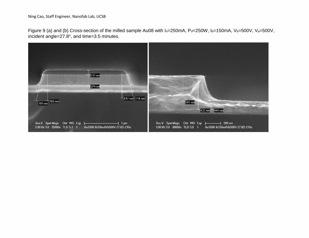
Figure 9 (a) and (b) Cross-section of the milled sample Au08 with In=250mA, Prf=250W, Ib=150mA, Vb=500V, Va=500V,
incident angle=27.8o, and time=3.5 minutes.

Ning Cao, Staff Engineer, Nanofab Lab, UCSB
Figure 10 (a) and (b) Cross-section of the milled sample Au09 with In=250mA, Prf=250W, Ib=50mA, Vb=500V, Va=500V,
incident angle=-27.8o, and time=14 minutes.

Ning Cao, Staff Engineer, Nanofab Lab, UCSB
Figure 11 (a) and (b) Cross-section of the milled sample Au10 with In=250mA, Prf=250W, Ib=50mA, Vb=500V, Va=500V,
incident angle=27.8o, and time=14 minutes.

Ning Cao, Staff Engineer, Nanofab Lab, UCSB
Figure 12 (a) and (b) Cross-section of the milled sample Au11 with In=250mA, Prf=250W, Ib=100mA, Vb=500V, Va=500V,
incident angle=27.8o, and time=7 minutes.

Ning Cao, Staff Engineer, Nanofab Lab, UCSB
Figure 13 (a) and (b) Cross-section of the milled sample Au12 with In=250mA, Prf=250W, Ib=100mA, Vb=500V, Va=500V,
incident angle=-27.8o, and time=7 minutes.

Ning Cao, Staff Engineer, Nanofab Lab, UCSB
Figure 14 (a) and (b) Cross-section of the milled sample Au13 with In=250mA, Prf=200W, Ib=150mA, Vb=350V, Va=500V,
incident angle=27.8o, and time=5.5 minutes.

Ning Cao, Staff Engineer, Nanofab Lab, UCSB
Figure 15 (a) and (b) Cross-section of the milled sample Au14 with In=250mA, Prf=200W, Ib=150mA, Vb=200V, Va=500V,
incident angle=27.8o, and time=7 minutes.

Ning Cao, Staff Engineer, Nanofab Lab, UCSB
Figure 16 (a) and (b) Cross-section of the milled sample Au16 with In=250mA, Prf=250W, Ib=200mA, Vb=1000V,
Va=500V, incident angle=-27.8o, and time=140 s.

Ning Cao, Staff Engineer, Nanofab Lab, UCSB
Figure 17 (a) and (b) Cross-section of the milled sample Au17 with In=250mA, Prf=250W, Ib=150mA, Vb=1000V, Va=500V,
incident angle=27.8o, and time=3.5 minutes.
Ning Cao, Staff Engineer, Nanofab Lab, UCSB
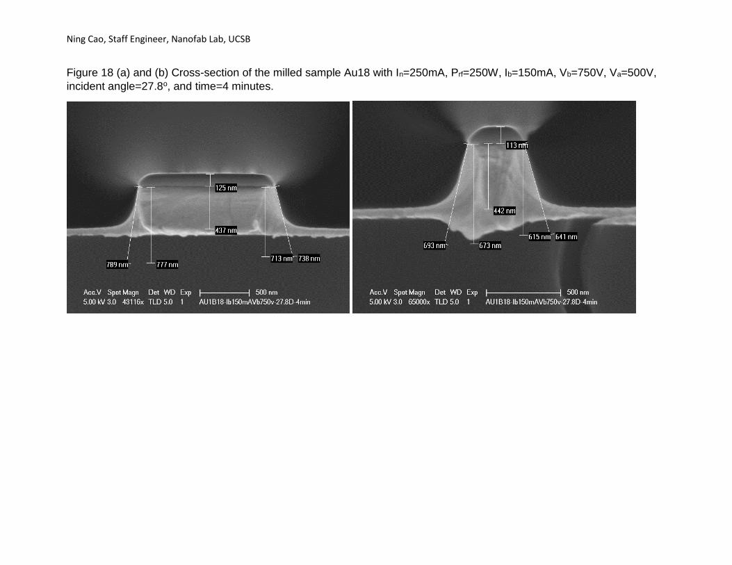
Figure 18 (a) and (b) Cross-section of the milled sample Au18 with In=250mA, Prf=250W, Ib=150mA, Vb=750V, Va=500V,
incident angle=27.8o, and time=4 minutes.
Ning Cao, Staff Engineer, Nanofab Lab, UCSB
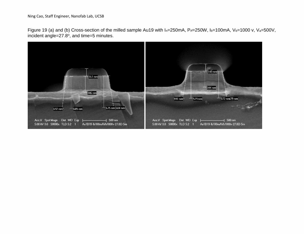
Figure 19 (a) and (b) Cross-section of the milled sample Au19 with In=250mA, Prf=250W, Ib=100mA, Vb=1000 v, Va=500V,
incident angle=27.8o, and time=5 minutes.
Ning Cao, Staff Engineer, Nanofab Lab, UCSB
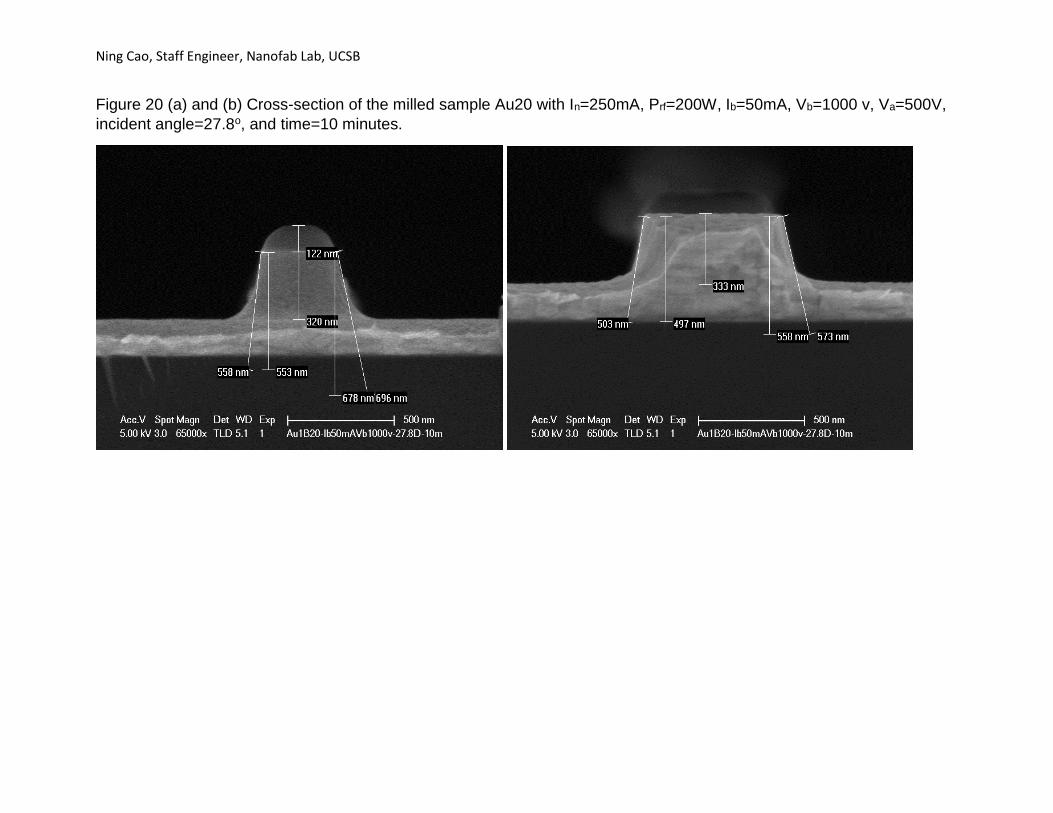
Figure 20 (a) and (b) Cross-section of the milled sample Au20 with In=250mA, Prf=200W, Ib=50mA, Vb=1000 v, Va=500V,
incident angle=27.8o, and time=10 minutes.

Ning Cao, Staff Engineer, Nanofab Lab, UCSB
Figure 21 (a) and (b) Cross-section of the milled sample Au21 with In=250mA, Prf=200W, Ib=25mA, Vb=1000 v, Va=500V,
incident angle=27.8o, and time=20 minutes.

Ning Cao, Staff Engineer, Nanofab Lab, UCSB
Figure 22 Etch rate of gold and selectivity (Au/Al2O3) as functions of Ar-ion Incident angle while keeping In=250mA,
Prf=250W, Ib=150mA, Vb=500V, and Va=500V.
0
2
4
6
8
10
12
14
16
18
20
70
75
80
85
90
95
100
105
110
115
120
-40 -30 -20 -10 0 10 20 30 40
Au etch rate and selectivity (Au/Al2O3) vs incident angle (In=250mA,Prf=250W, Ib=150mA, Vb=500V, Va=500V)
Etch Rate (nm/min)
Etch Selecltivity (Au/Al2O3)
Incident Angle (o)
Etch
Rat
e (
nm
/min
) Sele
ctivity (Au
/Al2 O
3 )

Ning Cao, Staff Engineer, Nanofab Lab, UCSB
Figure 23 Etched side-wall angle of gold as a function of Ar-ion Incident angle while keeping In=250mA, Prf=250W,
Ib=150mA, Vb=500V, and Va=500V.
60
62
64
66
68
70
72
74
76
78
80
-40 -30 -20 -10 0 10 20 30 40
Etched side-wall angle vs incident angle (In=250mA,Prf=250W, Ib=150mA, Vb=500V, Va=500V)
Incident Angle (o)
Sid
e-w
all A
ngl
e (
o)

Ning Cao, Staff Engineer, Nanofab Lab, UCSB
Figure 24 Etch rate and etch selectivity of gold as functions of beam current under the conditions of In=250mA, Vb=500 v,
Va=500 v, Ar Flow-rate=5 sccm for both neutralizer and beam, platen temperature=10oC, chamber wall
temperature=40oC, and platen rotation=20 rpm.
3
3.4
3.8
4.2
4.6
5
5.4
5.8
6.2
6.6
7
40 60 80 100 120 140 160
Etc
h S
elc
tivity
(Au
/Al2 O
3 )E
tch
Ra
te (
nm
)
Ib (mA)
Etch Rate and Selectivity of Gold vs Beam Current (In=250mA, Vb=500 v, Va=500 v, Ar Flow-rate=5 sccm for both neutralizer and beam, Platen temperature=10 C, Chamber wall
temperature=40 C, and Platen rotation=20 rpm)
Etch Rate (nm/min) (a=+27.8o)
Etch Rate (nm/min) (a=-27.8o)
Etch Selectivity (Au/Al2O3) (a=+27.8o)
Etch Selectivity (Au/Al2O3) (a=-27.8o)

Ning Cao, Staff Engineer, Nanofab Lab, UCSB
Figure 25 Sidewall angle of etched gold as a function of beam current under the conditions of In=250mA, Vb=500 v,
Va=500 v, Ar Flow-rate=5 sccm for both neutralizer and beam, platen temperature=10oC, chamber wall
temperature=40oC, and platen rotation=20 rpm.
40 60 80 100 120 140 160
Sid
ew
all A
ng
le (
o)
Ib (mA)
Sidewall Angle of Etched Gold vs Beam Current (In=250mA, Vb=500 v, Va=500 v, Ar Flow-rate=5 sccm for both neutralizer and beam, Platen temperature=10 C, Chamber wall
temperature=40 C, and Platen rotation=20 rpm)
Sidewall Angle (o) (a=+27.8o)
Sidewall Angle (o) (a=-27.8o)

Ning Cao, Staff Engineer, Nanofab Lab, UCSB
Figure 26 Etch rate and etched sidewall angle of gold as functions of beam voltage under the conditions of In=250mA,
Ib=150 mA, Va=500 v, incident angle=27.8o, Ar Flow-rate=5 sccm for both neutralizer and beam, platen
temperature=10oC, chamber wall temperature=40oC, and platen rotation=20 rpm.
70
71
72
73
74
75
76
77
78
79
80
10
20
30
40
50
60
70
80
90
100
110
0 200 400 600 800 1000 1200
Sidew
all An
gle ( o)
Etch
Rat
e (
nm
/min
)
Vb (v)
Au etch rate and sidewall angle vs beam voltage (In=250mA, Ib=150mA, Va=500v, incident angle=27.8o, Ar flowrate=5 sccm, Tp=10 C, Tch=40 C, and Platen rotation=20 rpm)
Etch Rate (nm/min)
Sidewall Angle (o)

Ning Cao, Staff Engineer, Nanofab Lab, UCSB
Figure 27 Etch selectivity (Au/Al2O3) as a function of beam voltage under the conditions of In=250mA, Ib=150 mA, Va=500
v, incident angle=27.8o, Ar Flow-rate=5 sccm for both neutralizer and beam, platen temperature=10oC, chamber wall
temperature=40oC, and platen rotation=20 rpm.
4
4.15
4.3
4.45
4.6
4.75
4.9
5.05
5.2
5.35
5.5
0 200 400 600 800 1000 1200
Etch
Se
lect
ivit
y (A
u/A
l 2O
3)
Vb (v)
Etch selectivity (Au/Al2O3) vs beam voltage (In=250mA, Ib=150mA, Va=500v, incident
angle=27.8o, Ar flowrate=5 sccm, Tp=10 C, Tch=40 C, and Platen rotation=20 rpm)
Etch Selectivity (Au/Al2O3)

Ning Cao, Staff Engineer, Nanofab Lab, UCSB
Figure 28 Etch rate and etch selectivity of gold as functions of beam current under the conditions of In=250mA, Vb=1000 v,
Va=500 v, incident angle=27.8o, Ar Flow-rate=5 sccm for both neutralizer and beam, platen temperature=10oC, chamber
wall temperature=40oC, and platen rotation=20 rpm.
70
71
72
73
74
75
76
77
78
79
80
10
20
30
40
50
60
70
80
90
100
110
0 20 40 60 80 100 120 140 160
Sidew
all An
gle ( o)
Etch
Rat
e (
nm
/min
)
Ib (v)
Au etch rate and sidewall angle vs beam current (In=250mA, Vb=1000 v, Va=500 v, Incidend angle=27.8o, Ar flowrate=5 sccm, Tp=10 C, Tch=40 C, and Platen rotation=20rpm)
Etch Rate (nm/min)
Side-wall Angle (o)

Ning Cao, Staff Engineer, Nanofab Lab, UCSB
Figure 29 Sidewall angle of etched gold as a function of beam current under the conditions of In=250mA, Vb=500 v,
Va=500 v, incident angle=27.8o, Ar Flow-rate=5 sccm for both neutralizer and beam, platen temperature=10oC, chamber
wall temperature=40oC, and platen rotation=20 rpm.
0
0.8
1.6
2.4
3.2
4
4.8
5.6
6.4
7.2
8
0 20 40 60 80 100 120 140 160
Etch
Se
lect
ivit
y (A
u/A
l 2O
3)
Ib (v)
Etch selectivity (Au/Al2O3) vs beam current (In=250mA, Vb=1000 v, Va=500 v, Incident angle=27.8o, Ar flowrate=5 sccm, Tp=10 C, Tch=40 C, and Platen rotation=20 rpm)
Selectivity (Au/Al2O3)