evaluation of stencil technology for miniaturization
TRANSCRIPT

EVALUATION OF STENCIL TECHNOLOGY FOR MINIATURIZATION
Neeta Agarwala Robert Farrella Joe Crudeleb
aBenchmark Electronics Inc., Nashua, NH, USA bBenchmark Electronics Inc., Rochester, MN, USA
Chrys Shea Shea Engineering Services
Burlington, NJ, USA
Ray Whittier Vicor Corporation, Andover, MA, USA
Chris Tibbetts Analogic Corporation, Peabody, MA, USA
ABSTRACT Miniature components are ubiquitous and require repeatable solder paste depositions to ensure a reliable interconnect and minimize rework. The objective of this study is to assess the impact of various stencil materials and fabrication methods on the repeatability of solder paste deposition. A test was designed to assess the performance of 18 different stencils, submitted by 6 different suppliers, using a variety of materials, coatings, and fabrication methods. Performance metrics include stencil aperture accuracy and topography, along with print volume repeatability and transfer efficiency for 0.4mm and 0.3 mm pitch BGAs and 0201 components with area ratios in the challenging range of 0.45 to 0.70.
INTRODUCTION SMT stencil printing technology continually evolves to keep pace with device miniaturization technologies. Printed Circuit Board (PCB) assemblers have numerous new technology options to choose from, and need to determine the most effective ones to produce the highest quality and most reliable solder interconnections.
The objective of these tests was to identify the best stencil technology for high volume production of miniaturized SMT components. The solder paste used for this assessment was SAC305 Pb-free no clean, Type 4 mesh. The specified stencil thickness for all stencils was 4mils (100µm).
EXPERIMENTAL SETUP Test Vehicle The test vehicle shown in Figure 1 was designed in-house for a multitude of PCB assembly tests, including new packages, pad designs, solder paste print performance and process evaluation tests. The devices selected for analysis in these tests included 0.3 and 0.4mm pitch BGAs and 0201s. Their area ratios ranged from 0.46 to 0.70. Locations and names of the specific devices used in the stencil analysis are shown in Figure 1.
Figure 1. Test Vehicle and features used in stencil analysis.
The recommended stencil thickness for the 0.3mm microBGA location is 3mils (75µm) versus the 4mil (100µm) thickness selected for this study. Consistent release for these apertures was not anticipated but relative comparisons of release would provide an indication of stencil performance.
Proceedings of SMTA International, Sep. 25 - 29, 2016, Rosemont, IL, USA Page 622
As originally published in the SMTA Proceedings

Test Design The stencil analysis included:
6 different stencil suppliers 9 different foil materials 5 different manufacturing processes 7 different nanocoatings
The experimental design was not a full factorial. Each supplier provided stencils using technologies that were either their top performers (High End), developmental technologies that they wanted to learn more about (Supplier choices #1 and #2), or lower cost stencils commonly ordered (AR>0.70). One to four stencils were submitted by each supplier. A total of 18 stencils were print tested. All were created using the same Gerber file, and all were specified at 0.0040” thick with identical apertures depending on the feature. The stencil test matrix is shown in Table 1. Table 1. Test Stencil Submissions
Supplier Letter Stencil No.
Type
A
1 Supplier choice #1
2 High End
3 AR>0.70
4 Supplier choice #2
B
5 AR>0.70
6 Supplier choice #2
7 Supplier choice #1
8 High End
C
9 Supplier choice #2
10 AR>0.70
11 High End
12 Supplier choice #1
D
13 High End
14 Supplier choice #1
15 Supplier choice #2
16 AR>0.70
E 17 AR>0.70
F 18 High End The Benchmark test vehicles were printed at the Benchmark Electronic Inc., Nashua, NH facility on a DEK 265 screen printer utilizing 18 stencils over a duration of 3 days. The solder paste was Pb-free, SAC305 no clean, Type 4 mesh. For each stencil, a total of six boards with a 10 minute delay between prints were printed by the same operator, using identical and common machine print parameters. The cards were printed in the same order and the underside of stencil was dry wiped after each print. All boards were measured with a Koh Young Solder Paste Inspection (SPI) platform. The 1st and 6th boards were photographed to provide a visual assessment of print repeatability; these images appear in Appendix I. Each stencil was photographed after
completion of the dry wipe following the 6th print. These images also appear in Appendix I and provide a relative comparison of paste release. Specifically, stencil apertures with the less amounts of paste indicate better release. STENCIL ASSESSMENT CRITERIA This study incorporated multiple parameters to assess stencil performance: Dimensional accuracy of the aperture opening or size
accuracy Visual assessment of the print and stencil after the final
print to determine the amount of paste remaining in the apertures
Topography of the aperture walls Analysis of SPI data for transfer efficiency and
repeatability Size Accuracy of the Apertures Miniature components require apertures that are within specification. Apertures that are too small increase the risk of insufficient solder defects due to poor paste release and apertures that are too large increase the risk of bridging and solder balls. Inconsistent apertures on 01005 or 0201 components increase the risk of tombstoning. The stencil providers were asked to include 4 small coupons outside the print area that could be removed and measured for accuracy and topography assessment. The latter is a destructive test. A stencil coupon is shown in Figure 2.
Figure 2. Stencil Coupon for F18. The coupon has 11 rows with various aperture openings in terms of size and shape, representing various components. Each row has 10 identical apertures to provide an indication of repeatability. The first row is a circular aperture with a specified diameter of 7.3 mils and the 2nd row is a square aperture with a specified length and width of 7.3 mils. These two rows are nearest the typical aperture for a 01005 component. The top side and bottom sides of coupon were measured at Vicor, using a Keyence digital microscope. The location of the aperture relative to the fiducial, or location accuracy, was not measured in this study. Each measurement was ranked as target condition (green), acceptable (yellow), or unacceptable (red). A green aperture measured within +/-.3 mils to the specification, a
Proceedings of SMTA International, Sep. 25 - 29, 2016, Rosemont, IL, USA Page 623

yellow was within +/- .3 to .5 mils, and red was outside of +/- .5 mils. The number of green, yellow and red ratings for each stencil was tabulated and the stencils ranked based on this criteria. The most accurate stencils did not have red ratings, and were ranked based on the highest number of green and fewest number of yellow ratings. The stencils with red ratings were ranked in descending order based on the number of red ratings. If two stencils had the same amount of red ratings, the number of green and yellow ratings was used to delineate the ranking. The summary appears in Table 2. Table 2. Stencils Ranking by Aperture size Accuracy
Stencil Number of Green Ratings (+/-.3 mils)
Number of Yellow Ratings (+/-.3 to .5 mils)
Number of Red Ratings (+/-.5 to .9 mils
Rank
B6 13 1 0 1
D16 13 1 0 1
C9 11 3 0 2
D14 11 3 0 2
B7 9 5 0 3
C10 9 5 0 3
E17 13 0 1 4
C11 12 1 1 5
C12 12 1 1 5
A2 9 4 1 6
B5 9 4 1 6
B8 9 4 1 6
A3 7 5 2 7
A4 7 5 2 7
D13 10 1 3 8
A1 5 4 5 9
F18 4 4 6 10
D15 6 0 8 11
Visual Assessment of Print and Stencil The visual assessments of paste deposits after the first and sixth print were performed at two selected fine pitch component pads 0.3mm microBGA and 0.4mm microBGA locations. Each stencil was also inspected after the final (sixth) print to have perspective on the amount of paste remaining in the apertures. The photos of uncleaned stencil apertures/windows at the same two component locations were also recorded after last or 6th print. Based solely on visual inspection, the stencils were grouped into the three categories shown in Table 3.
Table 3. Visual assessment of stencil apertures after 6th print. Representative photos are shown in Appendix I.
Supplier Ranking
A B C D E F
Above Average
A1 B5# B6B8
C11*
D16#
D14
Average A2 A4
B7 C9# C10
D15 E17
Below Average
A3 C12 D13 F18
* Stencil was noticed stained\rusted after final print and clean (photos in Appendix I) # Relatively clean stencil having small residual film after 6th print.
The photos of typical square shape apertures both regular and with radiuses corners are shown in Figure 3.
Figure 3. Square apertures with radiused corners The laser uses more energy to plunge into the middle of the aperture and less energy to provide a clean cut around the perimeter shown in Figure 4 from previous studies1-3.
Figure 4. Typical cutting path of a laser beam Topography of Aperture of Aperture Walls The roughness measurement was performed on the aperture walls of a test coupon for each stencil. The coupons were cut in half where indicated in Figures 5a and 5b, and four apertures were measured for each coupon. The topography comparison of A1 and C11 single aperture show a dramatic difference in roughness.
Proceedings of SMTA International, Sep. 25 - 29, 2016, Rosemont, IL, USA Page 624
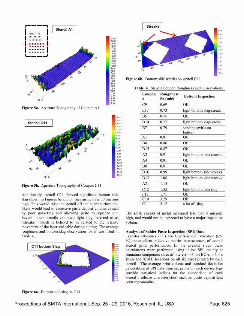
Figure 5a. Aperture Topography of Coupon A1
Figure 5b. Aperture Topography of Coupon C11 Additionally, stencil C11 showed significant bottom side slag shown in Figures 6a and b, measuring over 30 microns high. This would raise the stencil off the board surface and likely would lead to excessive paste deposit volume caused by poor gasketing and allowing paste to squeeze out. Several other stencils exhibited light slag, referred to as “streaks,” which is believd to be related to the relative movement of the laser and table during cutting. The average roughness and bottom slag observation for all are listed in Table 4.
Figure 6a. Bottom side slag on C11
Figure 6b. Bottom side streaks on stencil C11
Table 4. Stencil Coupon Roughness and Observations
Coupon#
Roughness Sa (mic)
Bottom Inspection
C9 0.69 OK
E17 0.73 light bottom slag/streak
B5 0.75 Ok
D14 0.77 light bottom slag/streak
B7 0.79 sanding swirls on bottom
A1 0.8 Ok
B6 0.86 Ok
D15 0.87 Ok
A3 0.9 light bottom side streaks
A4 0.91 Ok
B8 0.91 Ok
D16 0.99 light bottom side streaks
D13 1.08 light bottom side streaks
A2 1.15 Ok
C12 1.35 light bottom side slag F18 1.71 Ok C10 3.29 Ok C11 5.12 a lot of slag
The small streaks of metal measured less than 5 microns high, and would not be expected to have a major impact on volume. Analysis of Solder Paste Inspection (SPI) Data Transfer efficiency (TE) and Coefficient of Variation (CV %) are excellent indicative metrics in assessment of overall stencil print performance. In the present study these calculations were performed using inline SPI, mainly at miniature component sizes of interest: 0.3mm BGA, 0.4mm BGA and 0201H locations on all six cards printed by each stencil. The average print volume and standard deviation calculations of SPI data from six prints on each device type provide statistical indices for the comparison of each stencil’s release characteristics, such as paste deposit and print repeatability.
Stencil A1
Stencil C11
C11 bottom Slag
Streaks
Proceedings of SMTA International, Sep. 25 - 29, 2016, Rosemont, IL, USA Page 625

The aperture size at 0.3mmBGA, 0.4mm BGA and 0201H locations were measured directly on each stencil. The theoretical volume for each aperture was calculated. The specification defined area ratios for 0.3mm BGA-square, 0.4mm BGA-square and 0201s –circular shape features for 4 mil stencil thickness are 0.45, 0.55 and 0.70, respectively. The actual area ratios for these features not calculated in present work are slightly different on many stencils due to measured variation in actually cut aperture sizes. A similar study showed aperture size variation was generally within 2% on any given stencil, but as much as 22% different from stencil to stencil, which can have a considerable impact on the SMT process.3 Transfer efficiency (TE) is calculated as the ratio of average deposit volume to the aperture volume to obtain a measure of stencil’s print transferability. The Coefficient of Variation (CV %) is calculated as the ratio of standard deviation of paste volume to average paste volume and it serves as a measure of paste deposit repeatability from print to print. A generally accepted benchmark for acceptable paste transfer is 80% TE, with CV of 10% or less. Both TE and CV were determined and plotted for devices 0.3mm BGA, 0.4mm BGA and 0201s in Figures 7a and 7b.
Figure 7a. Stencil Transfer Efficiency
Figure 7b. Assessment of Stencil Print Repeatability RESULTS AND DISCUSSION For miniaturized components, many different stencil construction technologies were tested. A wide array of results were observed. The data indicates that the best performing stencils for the miniature components appear to be B5 and B6, and D14 and D16. Interestingly, B5 and D16 had no nanocoating on them. They were cut from name brand stainless steel on new, state-of-the-art cutters. B6 and D14 were also cut on new, state-of-the-art cutters and nanocoated with thermally cured fluoropolymer nanocoating. The electroformed stencil demonstrated the poorest size accuracy of the 18 stencils tested, which is in agreement with 3 previous studies since 2011.1-3 Stencils that were laser cut with nickel overplate did not appear to perform as well as laser cut SS without overplate, with or without nanocoating. New, investigative technologies that were tested show much promise for delivering quality prints at better price points, thereby representing better values to SMT assemblers. CONTINUING WORK One of the top performing stencils is currently the process of record on Vicor’s high volume production line. Because a large amount of production data already exists for this stencil configuration, a new one will not be ordered to run on the line. Instead, 2 other top performers and 2 stencils employing promising new technology will also be run for a full week in high volume production. The stencil with largest amount of slag and roughness will also be selected for volume runs to determine if these parameters impact end-of-line yields. The metrics for the production runs are, first and foremost, SPI yields. Secondary metrics include TE and Cpk for process control, and end-of-line yields.
0%
40%
80%
A1
A2
A3
A4
B5
B6
B7
B8
C10
C11
C12
C9
D13
D14
D15
D16
E17
F18
Stencil Transfer Efficiency 0.3mm BGA
0.4mm BGA
0201 Pads
Stencil
0
10
20
30
A1A2A3A4B5B6B7B8
C10
C11
C12 C9
D13
D14
D15
D16
E17
F18
0.3mmBGA
0.4mmBGA
0201Pads
Stencil
Coefficient ofVariation(CV%)
Proceedings of SMTA International, Sep. 25 - 29, 2016, Rosemont, IL, USA Page 626

Prior to the stencils entering production, they will be validated using SPI to measure 2 prints each on back and front strokes, and greater than 90% yield in the first hour of production. If print yields drop below 90% and the stencil is suspected as the root cause, it will be removed from the production line and replaced with the stencil used in the process of record to investigate the suspicion. Results from the longer term production study will be published at a later date. ACKNOWLEDGEMENTS The authors would like to sincerely acknowledge and thank: Nathan Taylor and Rey Molina of Benchmark
Electronics, NH for their technical support in execution of print tests and SPI programming.
Stan Camin of Vicor, MA for the measurements of stencil coupons.
Stencil providers for stencils and related technical support.
REFERENCES [1] Whittier, R. and Shea, C., “Evaluation of Stencil Materials, Suppliers and Coatings,” Proceedings of SMTA International Conference, September 2011. [2] Whittier, R. and Shea, C., “Fine Tuning The Stencil, Manufacturing Process and Other Stencil Printing Experiments” Proceedings of SMTA International Conference, September 2013. [3] Farrell, R. and Shea, C., “Stencil and Solder Paste Inspection Evaluation for Miniaturized Components” Proceedings of SMTA International Conference, September 2014.
Proceedings of SMTA International, Sep. 25 - 29, 2016, Rosemont, IL, USA Page 627

APPENDIX I
Solder paste deposit on 6th card
micro BGA apertures on stencil after 6th print
Solder paste deposit on 6th card
MicroBGA apertures on stencil after 6th print
Stencil D16
0.3mmBGA 0.4mmBGA
0.3mmBGA 0.4mmBGA
Stencil F18
0.3mmBGA 0.4mmBGA
0.3mmBGA 0.4mmBGA
Proceedings of SMTA International, Sep. 25 - 29, 2016, Rosemont, IL, USA Page 628