evbum2342db - implementing all‐in‐one pc power supply
TRANSCRIPT

© Semiconductor Components Industries, LLC, 2015
December, 2015 − Rev. 11 Publication Order Number:
EVBUM2342/D
EVBUM2342/D
Implementing All‐in‐One PCPower Supply EvaluationBoard User's Manual
PC Power Supply with the NCP1399,NCP1602, NCP4305, NCP4810 and NCP431
Table 1. GENERAL PARAMETERS
Devices Applications Input Voltage Output Power Topology Board Size
NCP1399NCP1602NCP4305NCP4810NCP431
AOI,Server Power
85 – 260 VAC 240 W CRM PFC & LLC 194 × 108 × 27 mm7.11 W/inch3
Output Voltage VOUT Ripple EfficiencyOperating
Temperature Cooling Standby Power
12 V/20 A(22 A Curr. Limit)
< 150 mV2 to 20 A
Load Steps
Above 89%@ ILOAD > 8 A
0–40°C Convection OpenFrame, Forced in
Frame
< 135 mW
DescriptionThis evaluation board user’s manual provides basic information
about a high efficiency, low no-load power consumption referencedesign that was tailored to power All-in-One PC or similar type ofequipment that accepts 12 VDC on the input. The power supplyimplements PFC front stage to assure unity power factor and lowTHD, current mode LLC power stage to enhance transient responseand secondary side synchronous rectification to maximize efficiency.This design note focuses mainly on the NCP1399 current mode LLCcontroller description – please refer to NCP1602 and NCP4305materials to gain more information about these devices.
The NCP1399 is a current mode LLC controller which means thatthe operating frequency of an LLC converter is not controlled viavoltage (or current) controlled oscillator but is directly derived fromthe resonant capacitor voltage signal and actual feedback level. Thiscontrol technique brings several benefits compare to traditionalvoltage mode controllers like improved line and load transientresponse and inherent out of zero voltage switching protection. TheLLC controller also features built-in high voltage startup and PFCoperation control pins that ease implementation of a power supplywith PFC front stage and no standby power supply on board. Theenhanced light lad operation scheme of the LLC controller allowsSMPS design to fulfill the latest no-load and light load consumptionlimits and still keep output voltage regulated with excellent transientresponse from no-load to full-load steps.
www.onsemi.com
EVAL BOARD USER’S MANUAL
Key Features• Wide Input Voltage Range
• High Efficiency
• Low No-load Power Consumption
• No Auxiliary SMPS
• Fast Startup
• X2 Capacitor Discharge Function
• Near Unity Power Factor
• Low Mains Protection
• Overload Protection
• Secondary Short Circuit Protected
• Thermal Protection
• Regulated Output Under any Conditions
• Excellent Load and Line TransientResponse
• All Magnetics Available as Standard Parts
• Small Form Factor
• Capability to Implement Off-mode forExtremely Low No-load PowerConsumption

EVBUM2342/D
www.onsemi.com2
Detail Demo-board Schematic Description
Figure 1. AOI Demo-board Schematic (Assembled Options on Standard Revision of the Demo, Refer to Figures 3 and 4 for Schematic Showing All Possible Options) − Primary Side

EVBUM2342/D
www.onsemi.com3
Figure 2. AOI Demo-board Schematic (Assembled Options on Standard Revision of the Demo, Refer to Figures 3 and 4 for Schematic Showing All Possible Options) − Secondary Side

EVBUM2342/D
www.onsemi.com4
Figure 3. AOI Demo-board Schematic (Assembled and also All Other Possible Options in PCB Layout) − Primary Side

EVBUM2342/D
www.onsemi.com5
Figure 4. AOI Demo-board Schematic (Assembled and also All Other Possible Options in PCB Layout) − Secondary Side

EVBUM2342/D
www.onsemi.com6
The input EMI filter is formed by components L15, L12,L13, C47, C33 Cy1, Cy2 and R48 – refer to Figure 1. Theinrush current limiting resistor R91 is replaced by strap inthis demo revision – one can replace it by appropriate NTCinrush current limiter if needed. The IC1 (NCP4810) withsafety resistors R53, R1, R16, R43 is used to assure lose-lessX2 capacitor discharge function after application isdisconnected from the mains.
The PFC power stage uses standard boost PFC topologyformed by power components B1, C15, L2, D4, D5, Q4, R38,and bulk capacitors C16, C38, C55. The PFC controller IC8(NCP1602) senses input voltage indirectly – via PFC powerMOSFET drain voltage sensing network R135, R134, R102and R101. The PFC coil current is sensed by the shunt resistorR38. The series resistor R80 defines maximum PFC frontstage peak current. The PFC feedback divider is shared withLLC brown-out sensing network in order to reduceapplication no-load power consumption. The PFC FB/LLCBO divider is formed by resistors R17, R28, R34, R46, R129,R132, R130 and R133. The FB signal is filtered by capacitorC26 to overcome possible troubles caused by the parasiticcapacitive coupling between pin and other nodes that handlehigh dV/dt signals. The internal bulk voltage regulatorcompensation C40, C36 and R75 is connected to the IC8 pin 1.The PFC MOSFET is driven via circuitry R25, D7, R26, R33and Q7. This solution allows to select needed turn-on andturn-off process speed for Q4 and also to handle gatedischarge current in local loop – minimizing EMI caused bythe driver loop. The PFC coil auxiliary winding providesbias for PFC and also LLC controllers during startup phase.Charge pump R72, C35, D14 and D20 is implemented for thispurpose.
The LLC power stage primary side composes fromthese devices: MOSFETs Q3, Q5, external resonant coil L3,transformer TR1 and resonant capacitors C7, C18. The IC3(NCP1399AA) LLC controller senses primary currentindirectly – via resonant capacitor voltage monitoring whichis divided down by capacitive divider C17, C29, C32 and C62.The capacitive divider has to provide minimum phase shiftbetween resonant capacitor signal and divided signal on theLLC_CS pin. The capacitive divide has to be loaded in thesame time to assure fast LLC_CS pin signal stabilizationafter application startup – this is achieved by resistor R148.The series resistor R64 is used to limit maximum current thatcan flow into the LLC_CS pin. The FB optoucoupler OK1is connected to the LLC_FB pin and defines converteroutput voltage by pulling down this pin when lower outputpower is needed. Capacitor C50 forms high frequency polein FB loop characteristics and helps to eliminate eventualnoise that could be coupled to the FB pin by parasiticcoupling paths. The Brow-out resistor sensing network wasalready described in PFC section as it is shared with PFCfeedback sensing. The Skip/REM pin of the NCP1399 isused for skip threshold adjustment. Resistors R103 and R104are used for this purpose together with noise filteringcapacitor C57. The over-voltage and over-temperature
protections are implemented via OVP/OTP pin by usingresistors R126 and R67, temperature dependent resistorNTC1, zener diode D21, filtering capacitor C44 andoptocoupler OK3. The OVP comparator is located on thesecondary side to assure maximum OVP circuitry accuracy.The PFC ON/OFF function is not used in this revision ofdemo-board – i.e. the bulk voltage is regulated to nominallevel during entire board operation (full, medium, light orno-load conditions) thus the P_ON/OFF pin is connected toground via resistor R105. The PFC_MODE pin provides biasto the PFC controller via series resistor R100 after highenough voltage is available on the LLC VCC capacitors C37.The VCC decoupling capacitor C54 and also bootstrapcapacitor for high side driver powering C53 are located asclose to the LLC controller package as possible to minimizeparasitic inductive coupling to other IC adjust componentsdue to high driver current peaks that are present in the circuitduring drivers rising and falling edges transitions. Thebootstrap capacitor is charged via HV bootstrap diode D23and series resistor R96 which limits charging current andVboot to HB power supply slope during initial C53 chargingprocess. The gate driver currents are reducer by added seriesresistors R54, R55 to optimize EMI signature of theapplication.
The primary controllers bias voltage limiter circuitryis used in order to restrict upper value of the primary VCCvoltage to approximately 13 V. The VCC limiter composesof these components: resistors R4, R150, capacitors C2, C3,diodes D3, D2, D26 and transistor Q6.
The secondary side synchronous rectification uses IC4and IC5 SR controllers – NCP4305. Two MOSFTEs areconnected in parallel for each SR channel to achieve lowtotal drop − Q2, Q9 and Q20, Q21. RC snubber circuits C4, R8,R9 and C25, R40, R41 are used to damp down the parasiticringing and thus limit the maximum peak voltage on the SRMOSFETs. The SR controllers are supplied from converteroutput via resistors R10 and R32. These resistors form RCfilter with decoupling capacitors C5, C6 and C19, C20. Theminimum on-time – R11, R39 and minimum off-time – R7,R37 resistors define needed blanking periods that help toovercome SR controllers false triggering to ringing in the SRpower stage. The light load detection circuit (LLD) isformed by resistors R109, R110 capacitor C59 and diodes D24,D25. The SR controllers are disabled by LLD circuitry whenapplication enters skip mode – this helps to reduce no-loadpower consumption of application. The trigger/disablefunction of NCP4305 is not used in this application thus thecorresponding pins are grounded. The output filteringcapacitor bank composes from low ESR capacitors C8 to C11and C21 to C24. Output filter L4, C12 is used to clean outoutput voltage from switching glitches.
The output voltage of the converter is regulated bystandard shunt regulator NCP431− IC6. The regulationoptocoupler OK1 is driven via resistor R85 which definesloop gain. The NCP431 is biased via resistor R88 in case thethere is no current flowing via regulation optocoupler –

EVBUM2342/D
www.onsemi.com7
which can happen before the nominal VOUT level is reachedor during transients from no-load to full-load conditions.The output voltage is adjusted by divider R89 and R98, R99.The feedback loop compensation network is formedpartially by resistor R95 and capacitor C51.
The secondary side OVP sense circuitry is also usingNCP431 reference (IC7) to achieve precise OVP trip point.The OVP threshold is adjusted by resistor divider R76, R77and R79. The bias current of OVP optoucoupler OK3 islimited by resistor R84 and IC7 is biased via resistor R82.Capacitor C30 slows down OVP reaction speed and helpsovercome false triggering by noise.
There are several options prepared in the PCB layout sothat customer can modify demo-board according to histarget application needs – please refer to Figure 4 forschematic that shows all options included in the PCB.Mentioned options for instance allow implementation ofoff-mode control from secondary side to further reduceno-load power consumption or different PFC front stagecontroller implementation.
Circuit LayoutThe PCB consists of a 2 layer FR4 board with 75 �m
copper cladding to minimize parasitic resistance insecondary side where high currents are conducted. Leadedcomponents are assembled form the top side of the board andall SMT components are place from the bottom only so thatwave soldering process can be used for production. Theboard was design to work as open frame with natural air flowcooling. The LLC transformer temperature reachesapproximately 90°C for Tambient = 25°C and full load.Forced air flow cooling management should be consideredin case the board is packed into some box or targetapplication.
Figure 5. Top Layer
Figure 6. Bottom Layer

EVBUM2342/D
www.onsemi.com8
Figure 7. Top Side Components
Figure 8. Bottom Side Components

EVBUM2342/D
www.onsemi.com9
Figure 9. Board Photo − Top Side
Figure 10. Board Photo − Bottom Side
EVBUM2342/D
www.onsemi.com10
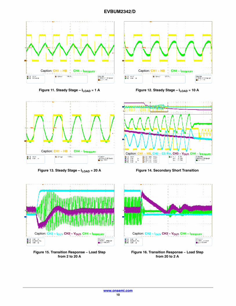
Figure 11. Steady Stage – ILOAD = 1 A Figure 12. Steady Stage – ILOAD = 10 A
Figure 13. Steady Stage – ILOAD = 20 A Figure 14. Secondary Short Transition
Figure 15. Transition Response − Load Stepfrom 2 to 20 A
Figure 16. Transition Response − Load Stepfrom 20 to 2 A
Caption: CH1 − HB CH4 − IPRIMARY Caption: CH1 − HB CH4 − IPRIMARY
Caption: CH1 − HB CH4 − IPRIMARY Caption: CH1 − HB, CH2 − CS Pin, CH3 − VOUT, CH4 − IPRIMARY
Caption: CH2 − IOUT, CH3 − VOUT, CH4 − IPRIMARYCaption: CH2 − IOUT, CH3 − VOUT, CH4 − IPRIMARY

EVBUM2342/D
www.onsemi.com11
Figure 17. Board Efficiency – Including PFC Stage
Figure 18. Board Power Stage with SR Efficiency VIN = 385 VDC
Output Current, IOUT (A)
Eff
icie
ncy
, � (
%)
Efficiency vs. Output Load VIN = 230 VAC
Efficiency vs. Output Load VIN = 110 VAC
0 2 4 6 8 10 12 14 16 18 2050
55
60
65
70
75
80
85
90
95
0 5 10 15 20
76
78
80
82
84
86
88
90
92
94
96
98
Output Current, IOUT (A)
Eff
icie
ncy
, � (
%)
Table 2. NO-LOAD INPUT POWER CONSUMPTION
Input Voltage Power Consumption
110 VAC 105 mW
230 VAC 129 mW

EVBUM2342/D
www.onsemi.com12
Table 3. BILL OF MATERIALS
Parts Qty Description Value Tolerance Footprint ManufacturerManufacturerPart Number
SubstitutionAllowed
B1 1 Bridge Rectifier KBU8M − KBU8M VishaySemiconductor
KBU8M−E4/51 Yes
C1, C13, C27,C28, C39,C43, C45,C46, C48,C49, C52,C56, C58,C63, C65,
C106, C107,C108, C109,C110, C111
21 Ceramic Capacitor NU − 0805 − − Yes
C12 1 Electrolytic Capacitor 220 �F/25 V 20% Through Hole PANASONIC EEU−FC1E221 Yes
C14 1 Electrolytic Capacitor NU − Through Hole − − Yes
C15, C33,C47
3 MKP Capacitor 1 �F/275 VAC 10% Through Hole Würth Elektronik MXXP225105K310ASPB46000
Yes
C16, C38,C55
3 Electrolytic Capacitor 100 �F/450 V 20% Through Hole Rubycon 450BXW100MEFC18X30 Yes
C17, C29 2 Ceramic Capacitor 220 pF/1 kV 20% Through Hole Vishay S221M39SL0N63K7R Yes
C2, C30, C32,C34, C57
5 Ceramic Capacitor 10 nF 10% 0805 Kemet C0805C103K5RACTU Yes
C26 1 Ceramic Capacitor 2.2 nF 10% 0805 Kemet C0805C222K5RACTU Yes
C3 1 Electrolytic Capacitor 220 �F/35 V 20% Through Hole PANASONIC EEU−FM1V221L Yes
C31 1 Ceramic Capacitor 2.2 �F 10% 1206 Kemet C1206C222K5RACTU Yes
C35 1 Ceramic Capacitor 6.8 nF 10% 0805 Kemet C0805C682K5RACTU Yes
C36 1 Ceramic Capacitor 1 �F 10% 0805 Kemet C0805C105K5RACTU Yes
C37 1 Electrolytic Capacitor 22 �F/35 V 20% Through Hole PANASONIC P15814CT−ND Yes
C4, C25 2 Ceramic Capacitor 3.9 nF 10% 1206 Kemet C1206C392K5RACTU Yes
C42 1 Electrolytic Capacitor NU − Through Hole − − Yes
C44 1 Ceramic Capacitor 100 pF 10% 0805 Kemet C0805C101K5RACTU Yes
C5, C19, C40,C41, C53,
C54
6 Ceramic Capacitor 100 nF 10% 0805 Kemet C0805C104K5RACTU Yes
C50 1 Ceramic Capacitor 470 pF 10% 0805 Kemet C0805C471K5RACTU Yes
C51 1 Ceramic Capacitor 2.7 nF 10% 0805 Kemet C0805C272K5RACTU Yes
C59 1 Ceramic Capacitor 22 nF 10% 0805 Kemet C0805C223K5RACTU Yes
C6, C20, 2 Ceramic Capacitor 1 �F 10% 1206 Kemet C1206C105K5RACTU Yes
C60, C61 2 Ceramic Capacitor NU − 1206 − − Yes
C62 1 Ceramic Capacitor 1 nF 10% 0805 Kemet C0805C102K5RACTU Yes
C7, C18 2 Metal Film Capacitor 15 nF/2 kVDC 5% Through Hole Vishay BFC238560153 No
C8, C9, C10,C11, C21,C22, C23,
C24
8 Electrolytic Capacitor 1,000 �F/16 V 20% Through Hole PANASONIC P15332CT−ND Yes
CY1, CY2,CY3
3 Ceramic Capacitor 2.2 nF/Y1/X1 20% Through Hole Murata DE1E3KX222MA5BA01 Yes
D1, D8 2 Power rectifier Diode MRA4007T3G − SMA ON Semiconductor MRA4007T3G No
D10, D11,D12, D13,D15, D16,
D105, D112
8 Diode NU − SOD−123 − − Yes
D17 1 Zener Diode 20 V 5% SOD−123 ON Semiconductor MMSZ20T1G No
D18, D19,D20, D27
3 Zener Diode NU − SOD−123 − − Yes
D2 1 Zener Diode 15 V 5% SOD−123 ON Semiconductor MMSZ15T1G No
D21 1 Zener Diode 4.3 V 5% SOD−123 ON Semiconductor MMSZ4V7T1G No
D23 1 Ultrafast PowerRectifier Diode
MURA160 − SMA ON Semiconductor MURA160T3G No
D26 1 Schottky Diode BAT54T1 − SOD−123 ON Semiconductor BAT54T1G No
D3 1 Schottky Diode MBR2H100SFT3G − SOD−123 ON Semiconductor MBR2H100SFT3G No
D4 1 Standard RecoveryRectifier Diode
1N5408 − Axial Lead ON Semiconductor 1N5408RLG No
D5 1 Soft RecoveryRectifier Diode
MSR860 − TO−220(2 LEAD)
ON Semiconductor MSRF860G No
D6, D9 2 Diode NU − SMA − − Yes

EVBUM2342/D
www.onsemi.com13
Table 3. BILL OF MATERIALS (continued)
PartsSubstitution
AllowedManufacturerPart NumberManufacturerFootprintToleranceValueDescriptionQty
D7, D14, D24,D25
4 Switching Diode MMSD4148 − SOD−123 ON Semiconductor MMSD4148T3G No
F1 − FUSE 1 Fuse, Medium Delay T−4A − − Bussmann TDC 210−4A Yes
F1 − Holder 1 Fuse Holder − − SH22.5A Multicomp MCHTC−15M Yes
F1 − Cover 1 Cover, PCB FuseHolder
− − − Multicomp MCHTC−150M Yes
HEATSINK_1 1 Heat Sink SK 454 150SA
− SK 454 150SA
Fischer Elektronik SK 454 150 SA Yes
HEATSINK_1 1 Heat Sink − − − − − Yes
IC1 1 X2 CapacitorDischarger
NCP4810 − SOIC−8 ON Semiconductor NCP4810DR2G No
IC101 1 Secondary SideSleep modeController
NU − SOIC−8 − − No
IC102 1 Secondary SideSleep modeController
NU − SOIC−8 − − No
IC2 1 Power FactorController
NU − SOIC−8 − − No
IC3 1 Resonant ModeController
NCP1399 − SOIC 16 ON Semiconductor NCP1399AADR2G No
IC4, IC5 2 Secondary SideSynchronous
Rectifier
NCP4305 − SOIC−8 ON Semiconductor NCP4305DDR2G No
IC6, IC7 2 ProgrammablePrecision Reference
NCP431 − SOT−23 ON Semiconductor NCP431AVSNT1G No
IC8 1 Power FactorController
NCP1602 − TSOP−6 ON Semiconductor NCP1602DCCSNT1G No
L2 1 PFC Inductor 260 �H 10% PQ3225 Würth Elektronik 750315036 Yes
L12, L13 2 Inductor 100 �H 20% DO5040H Coilcraft DO5040H−104MLB Yes
L15 1 Emi Filter 2.9 mH 15% TLBI ICE Components LF−28030−0029−H Yes
L3 1 Resonant Inductor 52 �H 10% RM8 Würth Elektronik 750370249 Yes
L4 1 Inductor 200 nH 20% L−US20A Bohemia Electric TC−05001510−00 Yes
L5, L6 2 Inductor NU − − − − Yes
L8 1 Inductor NU − − − − Yes
LED1 1 LED 3 mm NU − Through Hole − − Yes
NTC1 1 Thermistor 330 k� − Through Hole Vishay NTCLE100E3334JB0 Yes
OK1, OK3 2 Opto Coupler 817B − DIP−4 Fairchild FOD817B Yes
OK2 1 Opto Coupler NU − DIP−4 − − Yes
Q1 1 N-Channel MOSFET NU − SOT−23 − − Yes
Q10, Q100 2 PNP Transistror NU − SOT−23 − − Yes
Q11 1 PNP Transistror NU − SOT−23 − − Yes
Q12 1 NPN Transistor NU − SOT−23 − − Yes
Q2, Q9, Q20,Q21
4 N-Channel MOSFET NVMFS5830NL − SO−8FL/DFN−5
ON Semiconductor NVMFS5830NLT1G No
Q3, Q5 2 N-Channel MOSFET STP12NM50FP − TO−220 STMicroelectronics
STP12NM50FP Yes
Q4 1 N-Channel MOSFET STP20NM60FP − TO−220 STMicroelectronics
STP20NM60FP Yes
Q6 1 N-Channel MOSFET BSS138 − SOT−23 ON Semiconductor BSS138LT1G No
Q7 1 PNP Transistor BC807 − SOT−23 ON Semiconductor BC807−16LT1G No
Q8 1 N-Channel MOSFET BSS127 − SOT−23 DiodesIncorporated
BSS127S−7 No
R1, R16, R43,R53,
4 Resistor SMD 360 k� 1% 1206 RohmSemiconductor
MCR18ERTJ364 Yes
R10, R32 2 Resistor SMD 22 � 1% 0805 RohmSemiconductor
MCR10EZPF22R0 Yes
R104 1 Resistor SMD 130 k� 1% 0805 RohmSemiconductor
MCR10EZPF1303 Yes
R107 1 Resistor trough Hole,High Voltage
4.7 M� 5% 0414 Vishay VR37000004704JA100 Yes
R109 1 Resistor SMD 430 � 1% 0805 RohmSemiconductor
MCR10EZPF4300 Yes

EVBUM2342/D
www.onsemi.com14
Table 3. BILL OF MATERIALS (continued)
PartsSubstitution
AllowedManufacturerPart NumberManufacturerFootprintToleranceValueDescriptionQty
R11, R39 2 Resistor SMD 3.6 k� 1% 0805 RohmSemiconductor
MCR10EZPF3601 Yes
R12, R20,R33, R36,
R51
5 Resistor SMD 10 k� 1% 0805 RohmSemiconductor
MCR10EZPF1002 Yes
R126 1 Resistor SMD 5.1 k� 1% 0805 RohmSemiconductor
MCR10EZPF5101 Yes
R129 1 Resistor SMD 220 k� 1% 0805 RohmSemiconductor
MCR10EZPF2203 Yes
R132 1 Resistor SMD 30 k� 1% 0805 RohmSemiconductor
MCR10EZPF3002 Yes
R133 1 Resistor SMD 360 k� 1% 0805 RohmSemiconductor
MCR10EZPF3603 Yes
R134 1 Resistor SMD 2.7 M� 5% 1206 RohmSemiconductor
MCR18ERTJ275 Yes
R135 1 Resistor SMD 3 M� 5% 1206 RohmSemiconductor
MCR18ERTJ305 Yes
R148 1 Resistor SMD 1.5 k� 1% 0805 RohmSemiconductor
MCR10EZPF1501 Yes
R150 1 Resistor SMD 2 � 5% 0805 RohmSemiconductor
MCR10EZHJ2R0 Yes
R17, R28,R34, R46
4 Resistor SMD 1.8 M� 5% 0805 RohmSemiconductor
MCR25JZHJ185 Yes
R2, R3, R13,R24, R30,R49, R69,R78, R111,
R140, R142,R145, R147
13 Resistor SMD 0 � − 0805 RohmSemiconductor
MCR10EZPJ000 Yes
R25 1 Resistor SMD 47 � 1% 0805 RohmSemiconductor
MCR10EZPF47R0 Yes
R26 1 Resistor SMD 2.2 � 5% 0805 RohmSemiconductor
MCR10EZHJ2R2 Yes
R29, R94 2 Resistor SMD NU − 1206 − − Yes
R38 1 Power Resistor 0.0 �/3 W 1% Through Hole Vishay/Dale LVR03R0500FR50 Yes
R4, R82, R88 3 Resistor SMD 68 k� 1% 0805 RohmSemiconductor
MCR10EZPF6802 Yes
R42, R52,R68
3 Resistor SMD 0 � − 1206 RohmSemiconductor
MCR18EZHJ000 Yes
R44 1 Resistor SMD NU − 2010 − − Yes
R48 1 VARISTOR 275 VAC 1% Through Hole Würth Elektronik 820512711 Yes
R5, R6, R14,R15, R18,R19, R21,R22, R23,R27, R31,R35, R45,R47, R50,R56, R57,R58, R59,R60, R61,R62, R63,R65, R66,R70, R71,R73, R74,R81, R83,R86, R90,R93, R97,
R106, R108,R112, R113,R114, R115,R116, R117,R118, R119,R120, R121,R122, R123,R124, R125,R127, R128,R131, R136,R138, R141,R143, R144,R146, R149,
R151
62 Resistor SMD NU − 0805 − − Yes
R54, R55,R100
3 Resistor SMD 10 � 1% 0805 RohmSemiconductor
MCR10EZPF10R0 Yes
R64 1 Resistor SMD 100 � 1% 0805 RohmSemiconductor
MCR10EZPF1000 Yes

EVBUM2342/D
www.onsemi.com15
Table 3. BILL OF MATERIALS (continued)
PartsSubstitution
AllowedManufacturerPart NumberManufacturerFootprintToleranceValueDescriptionQty
R67 1 Resistor SMD 13 k� 1% 0805 RohmSemiconductor
MCR10EZPF1302 Yes
R7, R37,R130
3 Resistor SMD 22 k� 1% 0805 RohmSemiconductor
MCR10EZPF2202 Yes
R72 1 Resistor SMD 360 � 1% 0805 RohmSemiconductor
MCR10EZPF3600 Yes
R75, R79 2 Resistor SMD 82 k� 1% 0805 RohmSemiconductor
MCR10EZPF8202 Yes
R76, R95,R110
3 Resistor SMD 47 k� 1% 0805 RohmSemiconductor
MCR10EZPF4702 Yes
R77 1 Resistor SMD 12 k� 1% 0805 RohmSemiconductor
MCR10EZPF1202 Yes
R8, R9, R40,R41
4 Resistor SMD 27 � 1% 1206 RohmSemiconductor
MCR18ERTJ270 Yes
R80 1 Resistor SMD 43 k� 1% 0805 RohmSemiconductor
MCR10EZPF4302 Yes
R84, R105 2 Resistor SMD 1 k� 1% 0805 RohmSemiconductor
MCR10EZPF1001 Yes
R85 1 Resistor SMD 820 � 1% 0805 RohmSemiconductor
MCR10EZPF8200 Yes
R87, R92 2 Resistor SMD 2.7 k� 1% 1206 RohmSemiconductor
MCR18ERTF2701 Yes
R89 1 Resistor SMD 39 k� 1% 0805 RohmSemiconductor
MCR10EZPF3902 Yes
R91 1 NTC Thermistor 0 � 1% strap − − Yes
R96 1 Resistor SMD 5.6 � 5% 0805 RohmSemiconductor
MCR10EZHJ5R6 Yes
R98, R103 2 Resistor SMD 11 k� 1% 0805 RohmSemiconductor
MCR10EZPF1102 Yes
R99, R101,R102
3 Resistor SMD 150 k� 1% 0805 RohmSemiconductor
MCR10EZPF1503 Yes
TR1 1 Transformer 750314580 10% PQ3225 Würth Elektronik 750314580 Yes
X1 1 Output TerminalBlock
Pitch 5 mm − 20.700M/2 IMO 20.700M/2 Yes
X2 1 Input Terminal Block Pitch 5 mm − KRE 02 LUMBERG KRE 02 Yes
NOTE: All parts are Pb-Free.

www.onsemi.com1
onsemi, , and other names, marks, and brands are registered and/or common law trademarks of Semiconductor Components Industries, LLC dba “onsemi” or its affiliatesand/or subsidiaries in the United States and/or other countries. onsemi owns the rights to a number of patents, trademarks, copyrights, trade secrets, and other intellectual property. Alisting of onsemi’s product/patent coverage may be accessed at www.onsemi.com/site/pdf/Patent−Marking.pdf. onsemi is an Equal Opportunity/Affirmative Action Employer. Thisliterature is subject to all applicable copyright laws and is not for resale in any manner.
The evaluation board/kit (research and development board/kit) (hereinafter the “board”) is not a finished product and is not available for sale to consumers. The board is only intendedfor research, development, demonstration and evaluation purposes and will only be used in laboratory/development areas by persons with an engineering/technical training and familiarwith the risks associated with handling electrical/mechanical components, systems and subsystems. This person assumes full responsibility/liability for proper and safe handling. Anyother use, resale or redistribution for any other purpose is strictly prohibited.
THE BOARD IS PROVIDED BY ONSEMI TO YOU “AS IS” AND WITHOUT ANY REPRESENTATIONS OR WARRANTIES WHATSOEVER. WITHOUT LIMITING THE FOREGOING,ONSEMI (AND ITS LICENSORS/SUPPLIERS) HEREBY DISCLAIMS ANY AND ALL REPRESENTATIONS AND WARRANTIES IN RELATION TO THE BOARD, ANYMODIFICATIONS, OR THIS AGREEMENT, WHETHER EXPRESS, IMPLIED, STATUTORY OR OTHERWISE, INCLUDING WITHOUT LIMITATION ANY AND ALLREPRESENTATIONS AND WARRANTIES OF MERCHANTABILITY, FITNESS FOR A PARTICULAR PURPOSE, TITLE, NON−INFRINGEMENT, AND THOSE ARISING FROM ACOURSE OF DEALING, TRADE USAGE, TRADE CUSTOM OR TRADE PRACTICE.
onsemi reserves the right to make changes without further notice to any board.
You are responsible for determining whether the board will be suitable for your intended use or application or will achieve your intended results. Prior to using or distributing any systemsthat have been evaluated, designed or tested using the board, you agree to test and validate your design to confirm the functionality for your application. Any technical, applications ordesign information or advice, quality characterization, reliability data or other services provided by onsemi shall not constitute any representation or warranty by onsemi, and no additionalobligations or liabilities shall arise from onsemi having provided such information or services.
onsemi products including the boards are not designed, intended, or authorized for use in life support systems, or any FDA Class 3 medical devices or medical devices with a similaror equivalent classification in a foreign jurisdiction, or any devices intended for implantation in the human body. You agree to indemnify, defend and hold harmless onsemi, its directors,officers, employees, representatives, agents, subsidiaries, affiliates, distributors, and assigns, against any and all liabilities, losses, costs, damages, judgments, and expenses, arisingout of any claim, demand, investigation, lawsuit, regulatory action or cause of action arising out of or associated with any unauthorized use, even if such claim alleges that onsemi wasnegligent regarding the design or manufacture of any products and/or the board.
This evaluation board/kit does not fall within the scope of the European Union directives regarding electromagnetic compatibility, restricted substances (RoHS), recycling (WEEE), FCC,CE or UL, and may not meet the technical requirements of these or other related directives.
FCC WARNING – This evaluation board/kit is intended for use for engineering development, demonstration, or evaluation purposes only and is not considered by onsemi to be a finishedend product fit for general consumer use. It may generate, use, or radiate radio frequency energy and has not been tested for compliance with the limits of computing devices pursuantto part 15 of FCC rules, which are designed to provide reasonable protection against radio frequency interference. Operation of this equipment may cause interference with radiocommunications, in which case the user shall be responsible, at its expense, to take whatever measures may be required to correct this interference.
onsemi does not convey any license under its patent rights nor the rights of others.
LIMITATIONS OF LIABILITY: onsemi shall not be liable for any special, consequential, incidental, indirect or punitive damages, including, but not limited to the costs of requalification,delay, loss of profits or goodwill, arising out of or in connection with the board, even if onsemi is advised of the possibility of such damages. In no event shall onsemi’s aggregate liabilityfrom any obligation arising out of or in connection with the board, under any theory of liability, exceed the purchase price paid for the board, if any.
The board is provided to you subject to the license and other terms per onsemi’s standard terms and conditions of sale. For more information and documentation, please visitwww.onsemi.com.
PUBLICATION ORDERING INFORMATIONTECHNICAL SUPPORTNorth American Technical Support:Voice Mail: 1 800−282−9855 Toll Free USA/CanadaPhone: 011 421 33 790 2910
LITERATURE FULFILLMENT:Email Requests to: [email protected]
onsemi Website: www.onsemi.com
Europe, Middle East and Africa Technical Support:Phone: 00421 33 790 2910For additional information, please contact your local Sales Representative
◊