evbum2566db - implementing all‐in‐one pc power supply
TRANSCRIPT

© Semiconductor Components Industries, LLC, 2018
August, 2018 − Rev. 11 Publication Order Number:
EVBUM2566/D
EVBUM2566/D
Implementing All‐in‐One PCPower Supply EvaluationBoard User's Manual
PC Power Supply with the NCP13992,NCP1616, NCP4306 and NCP431
DescriptionThis evaluation board user’s manual provides basic information
about a high efficiency, low no-load power consumption referencedesign that was tailored to power All-in-One PC or similar type ofequipment that accepts 12 VDC on the input. The power supplyimplements PFC front stage to assure unity power factor and lowTHD, current mode LLC power stage to enhance transient responseand secondary side synchronous rectification to maximize efficiency.This design note focuses mainly on the NCP13992 current mode LLCcontroller description. Please use links in literature section to getmaterials about NCP1616, NCP4306 and NCP431 to gain moreinformation about these devices.
The NCP13992 is a high performance current mode controller forhalf bridge resonant converters. This controller implements 600 Vgate drivers, simplifying layout and reducing external componentcount. The Controller also features built-in high voltage startup. TheBrown-Out input function eases implementation of the controller in allapplications. In applications where a PFC front stage is needed, theNCP13992 features a dedicated output to drive the PFC controller.This feature together with quiet skip mode technique further improveslight load efficiency of the whole application. The NCP13992provides a suite of protection features allowing safe operation in anyapplication. This includes: overload protection, over-currentprotection to prevent hard switching cycles, brown-out detection, openoptocoupler detection, automatic dead-time adjust, over-voltage(OVP) and over-temperature (OTP) protections. The LLC currentmode means that the operating frequency of an LLC converter is notcontrolled via voltage (or current) controlled oscillator but is directlyderived from the resonant capacitor voltage signal and actual feedbacklevel. This control technique brings several benefits compare totraditional voltage mode controllers like improved line and loadtransient response and inherent out of zero voltage switchingprotection.
Table 1. GENERIC PARAMETERS
Device Applications Input VoltageNominal OutputVoltage/Current Output Power VOUT Ripple
NCP1616,NCP13992, NCP4306
AOI, Server Power
90 – 265 Vac 12 Vdc / 20 A 240 W < 150 mV@ Full load
Efficiency@ 230 V AC Standby Power
OperatingTemperature Cooling Topology Board Size
4 point AVG 94.11% < 135 mW 0 – 40°C Convection OpenFrame, Forced in
Frame
PFC CrCMLLC + SR
194 × 108 × 27 mm7.11 W/inch3
www.onsemi.com
Figure 1. Evaluation Board Picture
EVAL BOARD USER’S MANUAL
Key Features• Wide Input Voltage Range
• High Efficiency
• Low No−load Power Consumption
• No Auxiliary SMPS, Fast Startup
• X2 Capacitor Discharge Function
• Near Unity Power Factor
• Low Mains & Overload Protection
• Thermal Protection
• Regulated Output Under any Conditions
• Excellent Load & Line Transient Response
• All Magnetics Available as Standard Parts
• Small Form Factor
• Universal Design for Multiple ControllersAssembling Possibilities
• Extremely Low No−load Consumption

EVBUM2566/D
www.onsemi.com2
Figure 2. AOI Demo-board Schematic − Primary Side (Assembled Options on Standard Revision of the Demo)
VDR H10S 275TS E
T−4A
2n2/Y12n2/Y1
1uF /275Vac
0.05R / 2W
22k
GN
D
1uF /275Vac
1uF /275Vac
820n100n
22k
22k
33nF /2kVdc
5k6
GN
D 100n
GN
D 2n2/Y1
4M7
V bulk
F C
PF
22N60
F C
PF
13N60
F C
PF
13N60
100
0R
22R
22R
100n
MS
R 860
5R 6
27k
FO
D817B
220p/1kV
10n
13k
0R
10n
GND
MU
R A
160
1N5408
strap
MB
R 2H
100S F
T3G
BC
807−16
47
1N4148
KBU810
33nF /2kVdc
NU NU
3n9
GN
D
+17V
22R
30k
2u2
GN
D
GN
DG
ND
0R
470p
GN
D
0R
15V
22k
10n
GN
D
220u/35V
1M81M81M61M6
0R20k
200k
100n
MB
R 0540
MB
R 0540
1R
1R
NC
P13992A
IOG
E V
B
GN
D
FO
D817B
100u/25
GN
D5k1
100p
GN
D 330k
20k
GN
D
BS
S 138
4k7
100u/450V
100u/450V
100u/450V
0R
1k5
GN
D
4V3
2R
BA
T54T
1
220p/1kV2k
90uH, 7447013
90uH, 7447013
GN
D
2k72k7
1n
GN
D
VC
C IN
T
VC C INT
GN
D
S K
129_GN
DL
75k
220n
MR A4007T 3G
MR A4007T 3G
BAT54T1
VC C INT
+17V220uF
/35V
GN
D
2k72k7
1N4148
1N4148 33k
1M
1n
0R
150k
0R
1N41480R
0R
0R
0R
0R
47k
10n
0R
1n
GN
D
86k
86k
0R
10n
GN
D
680k
330k
1N4148
1k
BS
S 138
GN
D
50uH, 750370249
NC
P1616A
1
GN
DG
ND
GN
D
GN
D
LN AC INPUT90 − 265Vac
R 48
F 1
C Y1C Y2
C 15
R 38
R 33
C 33
C 47
C 40
C 41
R 20
R 36
C 18
R 104
C 54
C Y
3
R 107
Q4
Q3
Q5
R 64
R 42
R 54
R 55
C 53
D5
R 96
R 105
3 4O
K1
C 29
C 34
R 67
R 72
C 57
D23
D4
R 91
D3
Q7
R 25
D7
B1
C 7
D9 D6
C 32
R 26
R 75
C 36
R 52
C 50
R 5
D2
R 4
C 2
C 3
R 18R 27R 35R 47
R 56
R 70
R 80
C 43
D13
D12
R 58
R 62
X2−1
X2−2
HV
_IN1
VB
/PF
C −
F B
3
R E
M4
LLC _F
B5
LLC _C
S6
OV
P/O
T P
7
P_O
N/O
F F
8M
OD
E9
VC
C10
GN
D11
MLO
W12
MU
P14
HB
15V
BO
OT
16IC
3
3 4O
K3
C 37
R 126
C 44
NT
C 1
R 133
Q6
R 66
C 38
C 55
C 16
R 147
R 148
D21
R 150
D26
C 17
R 63
L5L6
R 87R 92
C 62
HE
AT
S IN
K_1
R 137
C 66
D22
D28
D19
C 56
R 6R 15
D1
D8
R 28
R 31
C 31
R 34
342
5*2
1
P E
R 1
R 16
D14R 43
R 50
R 57
R 61
R 69
R 74
C 26
R 94
C 13
R 2
R 158
R 13
C 27
R 49
R 102D17
R 24
Q8
L1
F B
1
VC
NT
R L
3
F F
C N
T R
L4
S T
DB
Y/FA
ULT
2
C S
/ZC
D5
GN
D6
DR
V7
VC
C8
HV
10U
1
+
+
+
+
+
INT
INT
INT
+

EVBUM2566/D
www.onsemi.com3
Figure 3. AOI Demo-board Schematic − Secondary Side (Assembled Options on Standard Revision of the Demo)
1000u/16V
1000u/16V
1000u/16V
220u/25V
820R
39k
47k
11k
150k
2n7
GN
D1
1000u/16V
1000u/16V
1000u/16V
1000u/16V
1000u/16V
GN
D1
GN
D1
0R
68k
56R
56R
0R0R
5k6
36k
6n8
6n8
1uF100n
100n1uF
5k6
36k
22k
22k
4R 74R 7
56R
56R
NC
P 4306A
AA
ZZ
ZA
GN
D1
GN
D1
NC
P 4306A
AA
ZZ
ZA
GN
D1 G
ND
1
GND1
GND1 GND1GND1 GND1
GND1
GN
D1
GN
D1
NTMFS 5C 442
NTMFS 5C 442NTMFS 5C 442
NTMFS 5C 442
0R
47k
12k
10n
82k
68k
1k
GN
D1
NC P 431
NC
P 431
0R
0R
WW
006
27k
27k
GND1GND1
GND1 GND1
100n100n
100n100n
GN
D1
C 21
C 22
C 23
C 12
R 85
R 89
R 95
R 98
R 99
C 51
12
C 9
C 24
C 8
C 10
C 11
X1−1
X1−2
X1−3
X1−4
R 78
R 88
R 9
R 41
R 3R 30
R 39
R 37
C 25
C 4
C 6
C 5
C 19
C 20
R 11
R 7
R 12
R 51
R 10R 32
R 8
R 40
IC 4
DR
V8
GN
D7
T R
IG/D
IS5
C S
6
VC
C1
MIN
_TO
F F
2
MIN
_TO
N3
LLD4IC
5
DR
V8
GN
D7
T R
IG/D
IS5
C S
6
VC
C1
MIN
_TO
F F
2
MIN
_TO
N3
LLD4
Q20
Q21
Q2
Q9
R 68
12
R 76
R 77
C 30
R 79
R 82
R 84
IC 6A C
R
A C
R
IC 7
R 140R 142
L4
11 9*2
8
R 100
R 101
C 59
C 63
C 71
C 73
+
+
+
+
+
+
+
+
+

EVBUM2566/D
www.onsemi.com4
Figure 4. AOI Demo-board Schematic − Primary Side (Assembled and also All Other Possible Options in PCB Layout)
VDR H10S 275TS ET−4A
2n2/Y12n2/Y1
1uF/275Vac
0.05R / 2W
22k
GN
D
1uF/275Vac
1uF/275Vac
820nN
U100n
GN
D
22k
22k
33nF/2kVdc
5k6
NU
GN
D
GN
DNU
100n
NU
GN
D 2n2/Y1
4M7
V bulk
FC P F22N60
FC
P F
13N60
FC
P F
13N60
100
0R
22R22R
100n
MS
R 860
5R 6
27k
FO
D817B
NU
220p/1kV
10n
13k
0R
10n
GND
MU
R A
160
NU
1N5408
strap
NU
MB
R 2H
100S F
T3G
BC807−16
471N
4148
KB
U810
33nF/2kVdc
NU NU3n9G
ND
+17V
NU
22R
30k
2u2
GN
D
GN
DG
ND
0R
GN
D
GN
D
GN
D
470p
GN
D
0R
15V
22k
10n
GN
D
220u/35V
1M8
1M8
1M6
1M6
0R
20k
200k
100n
MB
R 0540
MB
R 0540
1R1R
NC
P1399A
IOG
E V
B
GN
D
NU
FO
D817B
100u/25
GN
D
5k1
GN
D
100p
GN
D 330k
GN
D
NU
NU
20k
GN
D
NU
BS
S 138
GN
D
4k7
NU
GN
D
100u/450V
100u/450V
100u/450V
NU
NU
0R
1k5
GN
D
4V3
1RB
AT
54T1
220p/1kV2k
90uH, 7447013
90uH, 7447013
GN
D
NU
2k72k7
1n
GN
D
NU
VC
C IN
T
VC C INT
GN
D
S K
129_GN
DL
NC
P1616A
1
GN
D
75k
220nN
U
NU
MR A4007T3G
MR A4007T3G
NU
NU
NU
NU
BA
T54T
1 VC
C IN
T
+17V
220uF/35V
GN
D
2k72k7
1N4148
1N4148
NU
33kGN
D
NU
1M
1n 0R
150k
0R
1N4148
0RN
U0R
NU
0R
NU
NU
0R
0RN
U
47k
NU
10n
0R
NU
NU
1n
GN
D
86k
86k
0R
10n
GN
D
680k
330k
NU
GN
D
1N4148
1k
BS
S 138
GN
D
50uH, 750370249
LN AC INP UT90 − 265Vac
Dual footprint
package
Dual footprint
package
Dual footprint
package
R 48
F1
C Y1C Y2
C 15
R 38
R 33
C 33
C 47
C 40
C 39
C 41
R 20
R 36
C 18
R 104
R 103
C 28
C 54
C 42
C Y
3
R 107
Q4
Q3
Q5
R 64 R
42
R 54
R 55
C 53
D5
R 96
R 105
3 4O
K1
R 71
C 29
C 34
R 67
R 72
C 57
D23
L12
D4
R 91
L13
D3
Q7
R 25
D7
B1
C 7
D9 D6C
32
R 97
R 26
R 75C
36
R 52
C 50
R 5
D2
R 4
C 2
C 3
R 18
R 27
R 35
R 47
R 56
R 70
R 80
C 43
D13
D12
R 58
R 62
X2−1
X2−2
HV
_IN1
VB
/P F
C −
FB
3
R E
M4
LLC _F
B5
LLC _C
S6
OV
P /O
TP
7
P _O
N/O
FF
8M
OD
E9
VC
C10
GN
D11
MLO
W12
MU
P14
HB
15V
BO
OT
16IC
3
3 4O
K2
3 4O
K3
C 37
R 126
C 44
NT
C 1
D11
R 132
R 133
C 46
Q6
R 66
C 35
C 38
C 55
C 16
R 144
R 146
R 147
R 148
D21
R 150
D26
C 17
R 63
L5L6
R 83
R 87
R 92
C 62
R 93
HE
AT
S IN
K_1
HV
FB
1*2
FB
2*2
R S
T3
FO
VP
/BU
V4*2
VC
NT
R L
5*2
FF
C N
TR
L6
FAU
LT7
S T
DB
Y8
P S
TM
R9
P F
C O
K10
C S
/ZC
D11
GN
D12*2
DR
V13*2
VC
C14
HV
16*2U
1
R 137C
66C
67
NT
C 2
D22
D28
R 17 C
68
D18
R 14
D19
C 56
R 6
R 15
D1
D8
R 23
R 28
R 29
R 31
C 31
R 34
342
5*2
1
PE
R 1
R 16
D14
R 43
R 46
R 50
R 53
R 57 R
59R
60
R 61
R 69
R 73
R 74
R 81
C 26
R 94
D15
D16
C 13
R 2
R 158
R 13
C 27
R 49
R 102
C 74
D17
R 24
Q8
L1
+
+
+
+
+
+
INT
INT
INT
+
2.5V

EVBUM2566/D
www.onsemi.com5
Figure 5. AOI Demo-board Schematic − Secondary Side (Assembled and also All Other Possible Options in PCB Layout)
1000u/16V
1000u/16V
1000u/16V
220u/25V
820R39k
47k
11k150k
2n7
NU
GN
D1
GN
D1
1000u/16V
1000u/16V
1000u/16V
1000u/16V
1000u/16V
GN
D1
GN
D1
NU NU
NU
NU
GND1
0R
68k
56R
56R
0R
0R
5k6
36k
6n8
6n8
1uF100n
100n
1uF
5k6
36k
22k
22k
4R 7
4R 7
56R
56R
NC
P4306A
AA
ZZ
ZA
GN
D1
GN
D1
NC
P4306A
AA
ZZ
ZA
GN
D1
GN
D1
GN
D1
GND1 GND1
GND1 GND1
GN
D1
GN
D1
GN
D1
NTMFS 5C 442
NTMFS 5C 442
NTMFS 5C 442
NTMFS 5C 442
0R
GND1
NU NU
NU
NU
NU
NU
NU
NU
NUNUNU
NU
NU
NU
NU
NU
NU
NU
NU
NU
NU
NU
NU
NU
NU
NU
NU
NU(MMS D4148)
NU
NU
NU
NU
NU
47k
12k
10n
82k
68k
1k
GN
D1
NU
GN
D1
GN
D1
GND1GND1
GN
D1
GN
D1
NC P431
NC
P431
0R
NU
0R
NU
NU
NU
NU
WW
006
NU
NU
NU
27k
27k
NU
GND1
GND1
NU
GN
D1
GN
D1
100n100n
NUNU
NU
100n
NU
100n
C 21
C 22
C 23
C 12
R 85
R 89
R 95
R 98
R 99
C 51
C 49
12
C 9
C 24
C 8
C 10
C 11
X1−1
X1−2
X1−3
X1−4
C 48
R 86
D20
C 45
R 78
R 88
R 9
R 41
R 3
R 30
R 39
R 37
C 25
C 4
C 6
C 5
C 19
C 20
R 11
R 7
R 12
R 51
R 10
R 32
R 8
R 40
IC 4
DR
V8
GN
D7
TR
IG/D
IS5
C S
6
VC
C1
MIN
_TO
FF
2
MIN
_TO
N3
LLD4
IC 5
DR
V8
GN
D7
TR
IG/D
IS5
C S
6
VC
C1
MIN
_TO
FF
2
MIN
_TO
N3
LLD4
Q20
Q21
Q2
Q9
R 68
C 60 C 61
1212
C 1
R 19
C 106 R
21D
105
IS N
S4
VS
NS
1
OF
FD
E T
2
VM
IN3
VC
C8
DR
IVE
6
LE D
5
GN
D7
IC 101
R 117R 118R 127
R 119
R 120
C 108
R 22
C 111
R 128
R 116
C 109
LE D1
R 122
R 44
R 45
R 65
C 110
C 107
Q100
D112
R 125R 124
C 14 R 123
D10
R 76
R 77
C 30
R 79
R 82
R 84
R 90
FB
C6
GN
D7
IS N
S3
LE D
4
OF
FD
E T
2
ON
OF
F5
VC
C8
VS
NS
1
IC 6A C
R
A C
R
IC 7
R 140
R 141
R 142
R 143
Q10
R 121
R 131
L4
R 138
C 65
D27
11 9*2
8
R 100
R 101
C 52
C 58
C 59
C 63
C 64
C 69
C 70
C 71
C 72
C 73
+
+
+
+
+
+
+
+
+
+

EVBUM2566/D
www.onsemi.com6
Detailed Descriptions of the Evaluation BoardThe input EMI filter is formed by components L15, L5,
L6, C47, C33, CY1, CY2 and R48 – refer to Figure 2. Theinrush current limiting resistor R91 is substituted by strap inthis demo revision – one can replace it by appropriate NTCinrush current limiter if needed. The U1 − NCP1616(Figure 2) with diodes D22, D28 and resistors R6, R15 isused to X2 capacitor discharge function after application isdisconnected from the mains. This circuit also provides PFCVcc Start-up feature and input voltage sensing, also is partlyshared for the LLC controller IC. The Power FactorCorrector (PFC) power stage uses standard boost PFCtopology formed by power components B1, C15, L2, D4,D5, Q4, R38, and bulk capacitors C16, C38, C55. The PFCcontroller U1 (NCP1616) senses input voltage directly viapin 10 (HV) through network above mentioned. The PFCinductor current is sensed by the shunt resistor R38. Theseries resistor R38 sets maximum PFC front stage peakcurrent. Maximum peak current level is to 10 A. The PFCfeedback divider is shared with LLC brown-out sensingnetwork in order to reduce application no-load powerconsumption. The PFC FB divider is formed by resistorsR18, R27, R35, R47, R158, R63, R56, R34, R69, R74 andR31. The FB signal is filtered by capacitor C13 and C31 toovercome possible difficulties caused by the parasiticcapacitive coupling between pin and other nodes that handlehigh dV/dt signals. The internal bulk voltage regulatorcompensation C40, C36, R75 is connected through R61 tothe U1 pin 3. The PFC MOSFET is driven via circuitry R25,D7, R26, R33 and Q7. This solution enables to define neededturn-on and turn-off process speed for Q4. The PNPtransistor Q7 is connected directly source of Q4 (not throughsensing shunt R38) to minimize discharge loop and thusallow fast turn off PFC switch and also minimizing EMIcaused by the driver loop. The PFC coil auxiliary windingvoltage after rectifying with D14 provides ZCD signal forPFC controller. The NCP1616 has shared pin 5 − CS/ZCDfor current limit and zero current detection. Duringturned-on Q4 is sensed and limited maximum input currentand after turning-off Q4 is detected zero current condition.The resistance of R66 should be bigger than 3.9 k� to avoidwrong detection of destroyed R38. Also, resistance R28should be reasonable high enough to limit no-load andlight-load consumption.
The LLC power stage primary side converter composesfrom these devices: MOSFETs Q3, Q5, external resonantinductor L1, transformer TR1 and resonant capacitors C7,C18. The IC3(NCP13992AIOGEVB) LLC controllersenses primary current indirectly – via resonant capacitorvoltage monitoring which is divided down by capacitivedivider C17, C29, C32 and C62.The capacitive divider hasto provide minimum phase shift between resonant capacitorsignal and divided signal on the LLC_CS pin. The capacitivedivider has to be loaded in the same time to assure fastLLC_CS pin signal stabilization after application startup –this is achieved by resistor R148.The series resistor R64 isused to limit maximum current that can flow into the
LLC_CS pin. The FB optocoupler OK1 is connected to theLLC_FB pin and defines converter output voltage by pullingdown this pin when lower output power is needed. CapacitorC51 forms high frequency pole in FB loop characteristicsand helps to eliminate eventual noise that could be coupledto the FB pin by parasitic coupling paths. The Brow-outsignal for LLC controller is derived from PFC feedbackdivider – described before. A voltage taken from node R13,R47 and R158, is impedance separated by voltage followerQ8, which helps to avoid influencing bulk voltageregulation. The voltage follower output feds R2 and R133divider, which is minimizing Q8 thresh-hold voltagetemperature dependency. Divider output is filtered with C34and connected to IC3 VB/PFC−FB pin. The Skip/REM pinof the NCP13992 issued for skip threshold adjustment.Resistors R103 and R104 are used for this purpose togetherwith noise filtering capacitor C57. The over-voltage andover-temperature protections are implemented viaOVP/OTP pin by using resistors R126 and R67, temperaturedependent resistor NTC1, Zener-diode D21, filteringcapacitor C44 and optocoupler OK3. The OVP comparatoris located on the secondary side to assure maximum OVPcircuitry accuracy. The pin 8 P_ON/OFF is actually used fordefining minimum feedback voltage – lower saturationlevel, which influences maximum switching frequency. Forthis purpose serve R105 and C26 decouples noise. Thestand-by mode − burst mode of the PFC stage and bulkvoltage are controlled by NCP13992 via MODE pin 9,which goes high during LLC stage switching and during idlefalls to low level. While skip mode operation occurs, theLLC controller forces the PFC controller into STAND-BYmode by the MODE pin 9 via circuitry R80, C43, R70 andR50. Positive hiccup mode is implemented such way, thatMODE pin influences FB divider and changes lower restartlevel from lower value to higher value. This is realized bynetwork with D17, R102 and 49. These changes help toachieve very low no-load consumption.
The VCC decoupling capacitor C54 and also bootstrapcapacitor for high side driver powering C53 are located asclose to the LLC controller package as possible to minimizeparasitic inductive coupling to other IC adjust componentsdue to high driver current peaks that are present in the circuitduring drivers rising and falling edges transitions. Thebootstrap capacitor is charged via HV bootstrap diode D23and series resistor R96 which limits charging current andVboot to HB power supply slope during initial C53 chargingprocess. The gate driver currents are reduced by added seriesresistors R54, R55 to optimize EMI signature of theapplication. For fastening the mosfets turn-off process areused serial R−D particles composed with R58−D13 andR62−D12. The primary controllers bias voltage limitercircuitry is used in order to restrict upper value of theprimary VCC voltage to approximately 13 V. The VCClimiter composes of these components: resistors R150,R4,R5 capacitors C2, C3, diodes D3, D26 and transistor Q6.Thesecondary side synchronous rectification uses IC4 and IC5

EVBUM2566/D
www.onsemi.com7
SR controllers – NCP4306. Two MOSFTEs are connectedin parallel for each SR channel to achieve low total drop −Q2, Q9 and Q20, Q21. RC snubber circuits C4, R8, R9 andC25, R40, R41 are used to damp down the parasitic ringingand thus limit the maximum peak voltage on theSRMOSFETs. The SR controllers are supplied fromconverter output via resistors R68, R10 and R32. Theseresistors form RC filter with decoupling capacitors C5, C6and C19, C20. The minimum on-time – R11, R39 andminimum off-time – R7, R37 resistors define neededblanking periods that help to overcome SR controllers falsetriggering to ringing in the SR power stage. Each SRcontroller uses very clever light load detection feature(LLD). After first incoming pulse from burst, the LLDfeature wakes-up controller from low power mode (50 �A)and prepare it to operate. As last pulse from the burst endscontroller enters to stand-by mode after defined period,which is set with resistor (R100 and R101). Instead of thecomplicated light-load guard circuitry, just one additionalresistor is needed for setup. The NCP4306 LLD featureoffers great benefits compare to the traditional solutions, inwhich SR operation and no-load consumption is much lessefficient. The output filtering capacitor bank composes fromlow ESR electrolytic capacitors C8 to C11, C21 to C24 andceramic capacitors C59 to C73. Output filter L4, C12 is usedto smooth output voltage from switching glitches. L4 is600 nH inductor in case of need can be replaced withdifferent product which enables higher dI/dt slope load. Theoutput voltage of the converter is regulated by standardshunt regulator NCP431−IC6. The regulation optocoupler
OK1 is driven via resistor R85 which defines loop gain. TheNCP431 is biased via resistor R88 in case there is no currentflowing via regulation optocoupler – which can happenbefore the nominal VOUT level is reached or duringtransients from no-load to full-load conditions. The outputvoltage is adjusted by divider R89 and R98, R99. Thefeedback loop compensation network is formed partially byresistor R95 and capacitor C51. The secondary side OVPsense circuitry is also using NCP431 reference (IC7) toachieve precise OVP trip point. The OVP threshold isadjusted by resistor divider R76, R77and R79. The biascurrent of OVP optocoupler OK3 is limited by resistor R84and IC7 is biased via resistor R82. Capacitor C30 slowsdown OVP reaction speed and helps overcome falsetriggering by noise. There are several options prepared in thePCB layout so that customer can modify demo-boardaccording to required of target application – please refer toFigure 4 and 5 for schematic that shows all options includedin the PCB. The PCB consists of a 2 layer FR4 board with70 �m copper thickness to minimize parasitic resistance insecondary side where high currents are conducted. Leadedcomponents are assembled form the top side of the board andall SMT components are place from the bottom only so thatwave soldering process can be used for production. Theboard was design to work as open frame with natural air flowcooling. The LLC transformer temperature reachesapproximately 90°C for Tambient = 25°C and full load.Forced air flow cooling management should be consideredin case the board is packed into some box or targetapplication.

EVBUM2566/D
www.onsemi.com8
Figure 6. Evaluation Board − Top Side Components
Figure 7. Evaluation Board − Bottom Side Components

EVBUM2566/D
www.onsemi.com9
Figure 8. Evaluation Board − Top Layer
Figure 9. Evaluation Board − Bottom Layer Blue

EVBUM2566/D
www.onsemi.com10
Figure 10. Evaluation Board Photograph − Top View
Figure 11. Evaluation Board Photograph− Bottom View

EVBUM2566/D
www.onsemi.com11
Figure 12. Overall Efficiency vs. Output Power
76
78
80
82
84
86
88
90
92
94
96
0 50 100 150 200 250
Eff
icie
ncy
[%
]
Output Power [W]
Overall Efficiency at 115 V AC
Overall Efficiency at 230 V AC
Table 2. EFFICIENCY DATA MEASURED AND AVERAGED FROM 10 BUILT DEMO_BOARDS
LOAD
Consumption [mW] of Efficiency [%]
@ 120 VAC @ 230 VAC
NO−LOAD < 115 mW < 125 mW
Load 250 mW 0,466 0,475
Load 500 mW 0,72 0,823
Load 20% − 4 A 90,22 91,47
Load 25% − 5 A 91,82 92,95
Load 50% − 10 A 93,39 94,36
Load 75% − 15 A 93,13 94,62
Load 100% − 20 A 92,57 94,5
4 point AVG 92,73 94,11

EVBUM2566/D
www.onsemi.com12
The following figures illustrate conduced EMI signatures under full loading for different input line voltage levels.
Figure 13. EMI Signature Comparison @ 120 VAC & Full-load (Measured MAX Peak)
Figure 14. EMI Signature Comparison @ 230 VAC & Full-load (Measured MAX Peak)
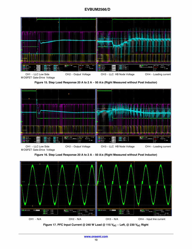
Figures 15 to 16 are focused on transient response, whichis highly depended (when is expected correct feedback loopbehavior) on loading current slope and output optional postfilter composed of L4 and C12. In case, that higher currentslope and lower voltage drop are needed inductor L4 can be
replaced by new one with lower inductance. Figure 17 showpower supply input current shape for different input linevoltage levels under full loading. Figures 18–20 areintended to LLC stage operation.
EVBUM2566/D
www.onsemi.com13
Figure 15. Step Load Response 20 A to 2 A − 50 A/s (Right Measured without Post Inductor)
Figure 16. Step Load Response 20 A to 2 A − 50 A/s (Right Measured without Post Inductor)
Figure 17. PFC Input Current @ 240 W Load @ 115 VAC − Left, @ 230 VAC Right
CH1 – LLC Low SideM OSFET Gate−Drive Voltage
CH2 – Output Voltage CH3 – LLC HB Node Voltage CH4 – Loading current
CH1 – LLC Low SideM OSFET Gate−Drive Voltage
CH2 – Output Voltage CH3 – LLC HB Node Voltage CH4 – Loading current
CH1 – N/A CH2 – N/A CH3 – N/A CH4 – Input line current

EVBUM2566/D
www.onsemi.com14
Figure 18. LLC Stage Start-up Sequence into Full-load Detail − Left, LCC Stage NO-LOAD Burst Detail − Right
Figure 19. LLC Stage SKIP Mode Operation at 0.5 A Load (Burst Detail) − Left, Light-load Mode Operation at 2 A Load − Right
Figure 20. LLC Stage Normal Operation 10 A Load − Left, LLC Stage Normal Operation 20 A Load − Right
CH1 – LLC Low SideM OSFET Gate−Drive Voltage
CH2 – N/A CH3 – LLC HB Node Voltage CH4 – Resonant tank current
CH1 – LLC Low SideM OSFET Gate−Drive Voltage
CH2 – N/A CH3 – LLC HB Node Voltage CH4 – Resonant tank current
CH1 – LLC Low SideM OSFET Gate−Drive Voltage
CH2 – N/A CH3 – LLC HB Node Voltage CH4 – Resonant tank current

EVBUM2566/D
www.onsemi.com15
Figure 21. PFC Vbulk Building @ 230 VAC @ 20 A Load − Left, PFC SKIP MODE at 0.5 A Load (Burst Detail) − Right
Figure 22. PFC, DCM @ 120 VAC 1.5 A Load − Left, PFC, CrM @ 120 VAC 20 A Load − Right
Figure 23. SR Waveforms during VOUT Building into Full Load − Left, SR NORMAL MODE @ Load 20 A − Right
CH1 – PFC M OSFET Gate−Drive Voltage
CH2 – Bulk Voltage CH3 – PFC M OSFET DrainVoltage
CH4 – PFC inductor current
CH1 – PFC M OSFET Gate−Drive Voltage
CH2 – Bulk Voltage CH3 – PFC M OSFET DrainVoltage
CH4 – PFC inductor current
CH1 – PFC M OSFET Gate−Drive Voltage
CH2 – Bulk Voltage CH3 – PFC M OSFET DrainVoltage
CH4 – PFC inductor current

EVBUM2566/D
www.onsemi.com16
Figure 24. SR Waveforms during Overload from 20 A to 25 A (FB Fault 100 ms) − Left, SR Waveforms during Hard Overload from 20 A to 50 A (CS Stop) − Right
CH1 – SR1 V DS Voltage CH1 – SR2 V DS Voltage CH3 – Output Voltage CH4 – Load current
Literature• High Performance Current Mode Resonant Controller with Integrated High Voltage Drivers:
NCP13992: http://www.onsemi.com/PowerSolutions/product.do?id=NCP13992
• Power Factor Controller, High Voltage Active X2:NCP1616: http://www.onsemi.com/PowerSolutions/product.do?id=NCP1616
• Secondary Side Synchronous Rectifier Controllers:NCP4306: http://www.onsemi.com/PowerSolutions/product.do?id=NCP4306
• Voltage Reference, Programmable Shunt Regulator:NCP431: http://www.onsemi.com/PowerSolutions/product.do?id=NCP431
• N-Channel SupreMOS® MOSFET 600 V, 22 A, 165 m�
FCPF22N60NT: http://www.onsemi.com/PowerSolutions/product.do?id=FCPF22N60NT
• Power Rectifier, Soft Recovery, Switch-mode, 8 A, 600 VMSR860: http://www.onsemi.com/PowerSolutions/product.do?id=MSRF860G
• N-Channel SupreMOS® MOSFET 600 V, 13 A, 258 m�
FCPF13N60NT: http://www.onsemi.com/PowerSolutions/product.do?id=FCPF13N60NT
• Single N-Channel Power MOSFET 40 V, 130 A, 2.5 m�
NVMFS5C442NL: http://www.onsemi.com/PowerSolutions/product.do?id=NVMFS5C442NL

EVBUM2566/D
www.onsemi.com17
Table 3. BILL OF MATERIALS
Reference Qty. Description Value Footprint ManufacturerManufacturerPart Number Substitution
B1 1 Bridge Rectifier KBU8M Through Hole Vishay KBU8M−E4/51 Yes
C12 1 Electrolytic Capacitor 220 �F/25 V Through Hole Panasonic EEU FC1E221 Yes
C13, C31, C62 3 Ceramic Capacitor 1 nF/50 V C 0805 Various
C15, C33, C47 3 MKP Capacitor 1 �F/275 Vac Through Hole Würth Elektronik MXXP225105K310ASPB46000
Yes
C16, C38, C55 3 Electrolytic Capacitor 100 �F/450 V Through Hole Rubycon 450BXW100MEFC18X30 Yes
C17, C29 2 Ceramic Capacitor 220 pF/1 kV Through Hole Vishay S221M39SL0N63K7R Yes
C2, C26, C27, C30,C34, C57
6 Ceramic Capacitor 10 nF/50 V C 0805 Various − Yes
C3 1 Electrolytic Capacitor 220 �F/35 V Through Hole Panasonic EEU FM1V221L Yes
C32 1 Ceramic Capacitor 39 nF/50 V C 0805 Various − Yes
C36 1 Ceramic Capacitor 2.2 �F/16 V C 0805 Various − Yes
C37 1 Electrolytic Capacitor 100 �F/25 V Through Hole Panasonic EEU−TA1E101BJ Yes
C4, C25 2 Ceramic Capacitor 6.8 pF/50 V 1206 Various − Yes
C40 1 Ceramic Capacitor 820 nF/16 V C 0805 Various − Yes
C44 1 Ceramic Capacitor 100 pF/50 V C 0805 Various − Yes
C5, C19, C41, C43,C53, C54, C59, C63,
C71, C73
10 Ceramic Capacitor 100 nF/50 V C 0805 Various − Yes
C50 1 Ceramic Capacitor 470 pF/50 V C 0805 Various − Yes
C51 1 Ceramic Capacitor 27 nF/50 V C 0805 Various − Yes
C56 1 Electrolytic Capacitor 220 �F/35 V Through Hole Panasonic EEU FM1V221L Yes
C6, C20 2 Ceramic Capacitor 1 �F/25 V C 0805 Various − Yes
C66 1 Ceramic Capacitor 220 nF/16 V C 0805 Various − Yes
C7, C18 2 Metal Film Capacitor 33 nF/630 V Through Hole Epcos B32652A6333J Yes
C8, C9, C10, C11,C21, C22, C23, C24
8 Electrolytic Capacitor 1000 �F/16 V Through Hole Panasonic P15332CT ND Yes
CY1, CY2, CY3 3 Y Capacitor 22 nF/Y1 Through Hole Murata DE1E3KX222MA5BA01
D1, D7, D8, D14,D17
5 Diode MMSD4148 SOD123 ON Semiconductor MMSD4148T3G No
D12, D13 2 Schottky Diode MBR0540 SOD123 ON Semiconductor MBR0540T1G No
D19, D26 2 Schottky Diode BAT54 SOD123 ON Semiconductor BAT54T1G No
D2 1 Zener Diode 15 V SOD123 ON Semiconductor MMSZ15T1G No
D21 1 Zener Diode 4.3 V SOD123 ON Semiconductor MMSZ4V3T1G No
D22, D28 2 Power Rectifier Diode MRA4007T3G SMA ON Semiconductor MRA4007T3G No
D23 1 Ultrafast PowerRectifier Diode
MURA160 SMA ON Semiconductor MURA160T3G No
D3 1 Schottky Diode MBR2H100 SOD123 ON Semiconductor MBR2H100SFT3G No
D4 1 Standard RecoveryRectifier Diode
1N5408 Through Hole ON Semiconductor 1N5408RLG No
D5 1 Soft RecoveryRectifier Diode
MSR860 TO220 ON Semiconductor MSRF860G No
D6, D9 2 Diode NU − − − −
F1 1 FUSE HOLDER +4A/T Fuse
T−4A Through Hole Various − Yes
IC3 1 LLC Controller NCP13992 NCP1399 ON Semiconductor NCP13992AIOGEVB No
IC4, IC5 2 SynchronousRectifier Controller
NCP4306 SOIC8 ON Semiconductor NCP4306AAAZZZA No
IC6, IC7 2 Shunt Regulator NCP431 SOT23 ON Semiconductor NCP431AVSNT1G No
L1 1 Power ResonantInductor
50 �H RM8 Würth Elektronik 750370249 Yes
L15 1 Common ModeInductor
2.9 mH Through Hole ICE Components LF−28030−0029−H No
L2 1 PFC Inductor 260 �H PQ3225 Würth Elektronik 750315036 Yes

EVBUM2566/D
www.onsemi.com18
Table 3. BILL OF MATERIALS (continued)
Reference SubstitutionManufacturerPart NumberManufacturerFootprintValueDescriptionQty.
L4 1 High Current Inductor 300 nH/30 A Through Hole Würth Elektronik WW006 Yes
L5, L6 2 EMI Inductor 90 �H Through Hole Würth Elektronik 7447013 Yes
NTC1 1 NTC Thermistor 330 k� Through Hole Vishay NTCLE100E3334JB0 Yes
OK1, OK3 2 Optocoupler FOD817B Through Hole ON Semiconductor FOD817B No
Q2, Q9, Q20, Q21 4 N−channel MOSFET NTMFS5C442 SO−8FL/DFN−5 ON Semiconductor NTMFS5C442NLTT1G No
Q3, Q5 2 N−channel MOSFET FCPF13N60 TO220 ON Semiconductor FCPF13N60NT No
Q4 1 N−channel MOSFET FCPF22N60 TO220 ON Semiconductor FCPF22N60NT No
Q6 1 N−channel MOSFET BSS138 SOT23 ON Semiconductor BSS138LT1G Yes
Q7 1 PNP Transistror BC807−16 SOT23 ON Semiconductor BC807−16LT1G Yes
Q8 1 N−channel MOSFET BSS138 SOT23 ON Semiconductor BSS138LT1G Yes
R1, R99 2 Resistor 150 k� R 0805 Various − Yes
R10, R32 2 Resistor 4.7 �/5% R 0805 Various − Yes
R100, R101, R105 3 Resistor 27 k� R 0805 Various − Yes
R102 1 Resistor 330 k� R 0805 Various − Yes
R107 1 Resistor 47 M�/5% Through Hole Vishay VR37000004704JA100 Yes
R11, R39, R104 3 Resistor 5.6 k� R 0805 Various − Yes
R126 1 Resistor 5.1 k� R 0805 Various − Yes
R137 1 Resistor 75 k� R 0805 Various − Yes
R148 1 Resistor 1.5 k� R 0805 Various − Yes
R150 1 Resistor 2 �/5% R 0805 Various − Yes
R18, R27 2 Resistor 1.8 M� R 0805 Various − Yes
R2, R158 2 Resistor 86 k� R 0805 Various − Yes
R24, R84 2 Resistor 1 k� R 0805 Various − Yes
R25 1 Resistor 47 �/5% R 0805 Various − Yes
R26, R54, R55 3 Resistor 22 �/5% R 0805 Various − Yes
R28 1 Resistor 33 k� R 0805 Various − Yes
R3, R5, R13, R16,R30, R34, R43, R50,R56, R57, R61, R69,
R72, R78, R94,R140, R142, R147
18 Resistor 0 � R 0805 Various − Yes
R31 1 Resistor 1 M� R 0805 Various − Yes
R35, R47 2 Resistor 1.6 M� R 0805 Various − Yes
R38 1 Resistor 0.05 �/3 W Through Hole Vishay/ Dale LVR03R0500FR50 Yes
R4, R12, R20, R33,R36, R51
6 Resistor 22 k� R 0805 Various − Yes
R42, R52, R68 3 Resistor 0 � R 1206 Various − Yes
R48 1 VARISTOR 275 VAC Through Hole Würth Elektronik 820512711 Yes
R49 1 Resistor 680 k� R 0805 Various − Yes
R58, R62 2 Resistor 1 �/5% R 0805 Various − Yes
R6, R15, R87, R92 4 Resistor 2.7 k� R 1206 Various − Yes
R63 1 Resistor 2 k� R 0805 Various − Yes
R64 1 Resistor 100 � R 0805 Various − Yes
R66 1 Resistor 4.7 k� R 0805 Various − Yes
R67 1 Resistor 13 k� R 0805 Various − Yes
R7, R37 2 Resistor 36 k� R 0805 Various − Yes
R70, R133 2 Resistor 20 k� R 0805 Various − Yes
R74, R76, R95 3 Resistor 47 k� R 0805 Various − Yes
R75 1 Resistor 30 k� R 0805 Various − Yes
R77 1 Resistor 12 k� R 0805 Various − Yes

EVBUM2566/D
www.onsemi.com19
Table 3. BILL OF MATERIALS (continued)
Reference SubstitutionManufacturerPart NumberManufacturerFootprintValueDescriptionQty.
R79 1 Resistor 82 k� R 0805 Various − Yes
R8, R9, R40, R41 4 Resistor 56 �/5% R 1206 Various − Yes
R80 1 Resistor 200 k� R 0805 Various − Yes
R82, R88 2 Resistor 68 k� R 0805 Various − Yes
R85 1 Resistor 820 � R 0805 Various − Yes
R89 1 Resistor 39 k� R 0805 Various − Yes
R91 1 VARISTOR strap − − − Yes
R96 1 Resistor 5.6 /5% R 0805 Various − Yes
R98 1 Resistor 11 k� R 0805 Various − Yes
TR1 1 LLC Transformer Lpri = 600 �H PQ3225 Würth Elektronik 750314580 Yes
U1 1 Power FactorController
NCP1616A1 SO9 ON Semiconductor NCP1616A1 No
X1 1 Wire to boardterminal
Pitch 5 mm Through Hole IMO 20.700M/2 Yes
X2 1 Wire to boardterminal
Pitch 5 mm Through Hole Lumberg KRE 02 Yes

www.onsemi.com1
onsemi, , and other names, marks, and brands are registered and/or common law trademarks of Semiconductor Components Industries, LLC dba “onsemi” or its affiliatesand/or subsidiaries in the United States and/or other countries. onsemi owns the rights to a number of patents, trademarks, copyrights, trade secrets, and other intellectual property. Alisting of onsemi’s product/patent coverage may be accessed at www.onsemi.com/site/pdf/Patent−Marking.pdf. onsemi is an Equal Opportunity/Affirmative Action Employer. Thisliterature is subject to all applicable copyright laws and is not for resale in any manner.
The evaluation board/kit (research and development board/kit) (hereinafter the “board”) is not a finished product and is not available for sale to consumers. The board is only intendedfor research, development, demonstration and evaluation purposes and will only be used in laboratory/development areas by persons with an engineering/technical training and familiarwith the risks associated with handling electrical/mechanical components, systems and subsystems. This person assumes full responsibility/liability for proper and safe handling. Anyother use, resale or redistribution for any other purpose is strictly prohibited.
THE BOARD IS PROVIDED BY ONSEMI TO YOU “AS IS” AND WITHOUT ANY REPRESENTATIONS OR WARRANTIES WHATSOEVER. WITHOUT LIMITING THE FOREGOING,ONSEMI (AND ITS LICENSORS/SUPPLIERS) HEREBY DISCLAIMS ANY AND ALL REPRESENTATIONS AND WARRANTIES IN RELATION TO THE BOARD, ANYMODIFICATIONS, OR THIS AGREEMENT, WHETHER EXPRESS, IMPLIED, STATUTORY OR OTHERWISE, INCLUDING WITHOUT LIMITATION ANY AND ALLREPRESENTATIONS AND WARRANTIES OF MERCHANTABILITY, FITNESS FOR A PARTICULAR PURPOSE, TITLE, NON−INFRINGEMENT, AND THOSE ARISING FROM ACOURSE OF DEALING, TRADE USAGE, TRADE CUSTOM OR TRADE PRACTICE.
onsemi reserves the right to make changes without further notice to any board.
You are responsible for determining whether the board will be suitable for your intended use or application or will achieve your intended results. Prior to using or distributing any systemsthat have been evaluated, designed or tested using the board, you agree to test and validate your design to confirm the functionality for your application. Any technical, applications ordesign information or advice, quality characterization, reliability data or other services provided by onsemi shall not constitute any representation or warranty by onsemi, and no additionalobligations or liabilities shall arise from onsemi having provided such information or services.
onsemi products including the boards are not designed, intended, or authorized for use in life support systems, or any FDA Class 3 medical devices or medical devices with a similaror equivalent classification in a foreign jurisdiction, or any devices intended for implantation in the human body. You agree to indemnify, defend and hold harmless onsemi, its directors,officers, employees, representatives, agents, subsidiaries, affiliates, distributors, and assigns, against any and all liabilities, losses, costs, damages, judgments, and expenses, arisingout of any claim, demand, investigation, lawsuit, regulatory action or cause of action arising out of or associated with any unauthorized use, even if such claim alleges that onsemi wasnegligent regarding the design or manufacture of any products and/or the board.
This evaluation board/kit does not fall within the scope of the European Union directives regarding electromagnetic compatibility, restricted substances (RoHS), recycling (WEEE), FCC,CE or UL, and may not meet the technical requirements of these or other related directives.
FCC WARNING – This evaluation board/kit is intended for use for engineering development, demonstration, or evaluation purposes only and is not considered by onsemi to be a finishedend product fit for general consumer use. It may generate, use, or radiate radio frequency energy and has not been tested for compliance with the limits of computing devices pursuantto part 15 of FCC rules, which are designed to provide reasonable protection against radio frequency interference. Operation of this equipment may cause interference with radiocommunications, in which case the user shall be responsible, at its expense, to take whatever measures may be required to correct this interference.
onsemi does not convey any license under its patent rights nor the rights of others.
LIMITATIONS OF LIABILITY: onsemi shall not be liable for any special, consequential, incidental, indirect or punitive damages, including, but not limited to the costs of requalification,delay, loss of profits or goodwill, arising out of or in connection with the board, even if onsemi is advised of the possibility of such damages. In no event shall onsemi’s aggregate liabilityfrom any obligation arising out of or in connection with the board, under any theory of liability, exceed the purchase price paid for the board, if any.
The board is provided to you subject to the license and other terms per onsemi’s standard terms and conditions of sale. For more information and documentation, please visitwww.onsemi.com.
PUBLICATION ORDERING INFORMATIONTECHNICAL SUPPORTNorth American Technical Support:Voice Mail: 1 800−282−9855 Toll Free USA/CanadaPhone: 011 421 33 790 2910
LITERATURE FULFILLMENT:Email Requests to: [email protected]
onsemi Website: www.onsemi.com
Europe, Middle East and Africa Technical Support:Phone: 00421 33 790 2910For additional information, please contact your local Sales Representative
◊