exhibition guide - spiespie.org/documents/conferencesexhibitions/spie... · reach a global audience...
TRANSCRIPT
EXHIBITION GUIDE•
Find the exhibitions that will help you reach qualified buyers, grow your revenue, and keep ahead of the competition.
201516

THE SPIE EXHIBITION FLOOR•The place to make profitable connections with a targeted audience of customers and prospects. The co-located technical conferences organized by SPIE attract scientists, engineers, system integrators and buyers from around the world.
In America, Asia, UK, France, and the rest of the world
SPIE Headquarters Tel: +1 360 676 3290 [email protected] www.spie.org/exhibits
E.Exhibitions.
SPIE EXHIBITIONS wORk FOR yOU•Brand Exposure – Gain the visibility that keeps your company top-of-mind with prospects and customers. Nothing replaces face-to-face interactions on the exhibition floor.
Tools to Grow Revenue – Ensure as much traffic as possible at your booth by booking early, with sponsorships, or advertising to give you extra visibility. Exhibiting with SPIE is a proven way to meet potential customers.
A Prequalified Audience – Build your marketing plan around the exhibitions where you will meet people who are looking for your solutions. Let the SPIE sales team help you find the exhibitions that are the best fit for your business.
SPIE Exhibitions help connect suppliers with customers, while educating the community about new technology.
In Europe excluding UK, Ireland, and France
Hermann Doster Tel: +49 (0)7025/841 806 Mob: +49 (0)152/046 096 44 [email protected]

Contents.
Photonics West . . . . . . . . . . . . . . . . . . . . . . . . . . . . . . . . 2
BiOS ExPO . . . . . . . . . . . . . . . . . . . . . . . . . . . . . . . . . . . . 4
Advanced Lithography . . . . . . . . . . . . . . . . . . . . . . . . . . 6
IS&T/SPIE Electronic Imaging . . . . . . . . . . . . . . . . . . . . 8
Optics + Optoelectronics . . . . . . . . . . . . . . . . . . . . . . . . 9
Smart Structures/NDE . . . . . . . . . . . . . . . . . . . . . . . . . 10
Photonics Europe . . . . . . . . . . . . . . . . . . . . . . . . . . . . . 12
DSS ExPO . . . . . . . . . . . . . . . . . . . . . . . . . . . . . . . . . . . . 14
Astronomical Telescopes + Instrumentation . . . . . . 16
Optics + Photonics . . . . . . . . . . . . . . . . . . . . . . . . . . . . 18
Photomask Technology . . . . . . . . . . . . . . . . . . . . . . . .20
Optifab . . . . . . . . . . . . . . . . . . . . . . . . . . . . . . . . . . . . . . 22
Security + Defence/Remote Sensing . . . . . . . . . . . . . 24
Exhibition Calendar. . . . . . . . . . . . . . .inside back cover
“We build our trade show schedule around SPIE Exhibitions.”
– Rob Morris Director of Marketing & Customer Relations, Ocean Optics, Inc.
www.spie.org/exhibitions

“Photonics West is the best meeting I have ever attended because the conference and exhibition bring
interdisciplinary science—physics, chemistry, biology and more—together with engineering. It’s fantastic.”
– James Wynne IBM Watson Research Center
PHOTONICS wEST•
This event always sells out. Sign up today!
PLAN FOR 2016Exhibition: 16–18 February 2016
Conferences & Courses: 13–18 February 2016
JOIN US IN 2015Exhibition: 10–12 February 2015
Conferences & Courses: 7–12 February 2015

kEy METRICS20,000 Attendees
1,250 Exhibitors
4,700 Technical Papers
65 Courses and Workshops
ATTENDEESApplication/design engineers
System integrators
Test and measurement engineers
Product and process developers
Purchasing executives
Scientists/Researchers
OEMs
Entrepreneurs/Executives
CONFERENCE TOPICSBiomedical optics/photonics
Optoelectronic devices
Lasers
LEDs
Photonic integration
Advanced quantum applications
Communication devices and materials
Nanotechnology
Displays and holography
MOEMS-MEMS
Industrial applications of lasers
3D Fabrication
Silicon photonics
EXHIBITION TECHNOLOGIESLaser sources and systems
Lenses and filters, optical components and materials
IR sources and detectors
Cameras and sensors
Electronic imaging components
Fiber optic systems
Optical coatings
Positioning and mounts
Metrology/test and measurement
Custom optics
Software for optical engineering
There is no other event on the photonics industry like SPIE Photonics West. With over 1,250 exhibitors and 20,000 attendees from over 40 countries, SPIE Photonics West is the global photonics marketplace. Every year more products are launched, more deals are made, and more collaboration occurs at Photonics West, the flagship event for the photonics and laser industry.
3
“The best trade show of the year and an opportunity for us to connect with both
new and old customers.”– Peter Brown
Sales and Marketing Manager, Lattice Materials
Experience the impact of SPIE Photonics West—the world’s largest photonics and laser event.
The Moscone Center San Francisco, California, USA

PLAN FOR 2016Exhibition: 13–14 February 2016
Conferences & Courses: 13–18 February 2016
JOIN US IN 2015Exhibition: 7–8 February 2015
Conferences & Courses: 7–12 February 2015
BIOS EXPO•PART OF SPIE PHOTONICS WEST
THE MOSCONE CENTER SAN FRANCISCO, CALIFORNIA, USA

5
“BiOS was a wonderful forum to show off our optical coatings technology. This is our first
year and we will be back.” – Donna Hooker
Deposition Sciences, Inc.
Connect with over 7,000 attendees, reach qualified buyers, and build the profitable relationships that can grow your business. This is the proven marketplace for your biophotonics products with more prospects than anywhere else, making it a cost-effective exhibition with real ROI. BiOS ExPO is the ideal place to interact with the developers and early adopters of the newest biophotonics technologies, as well as the best venue to introduce technologies and instrumentation for diagnostics, therapeutics, and imaging.
The world’s largest international biomedical optics exhibition
kEy METRICS7,000 Attendees
235 Exhibitors
2,100 Presentations
35 Conferences
20 Courses and Workshops
ATTENDEESMedical and optical physicists
Biomedical research clinicians
Optical instrument developers
Equipment designers
Physicians
Bioengineers
Cell physiologists
Cancer therapists
CONFERENCE TOPICSPhotonic therapeutics and diagnostics
Clinical technologies and systems
Tissue optics, laser-tissue interaction, and tissue engineering
Biomedical spectroscopy, microscopy, and imaging
Nano/biophotonics
Translational research
EXHIBITION TECHNOLOGIESMolecular imaging
Lasers
Biomedical optics and components
Instrumentation
Nano/biophotonics
Biosensors
Spectroscopy
Microscopic imaging
The Moscone Center San Francisco, California, USA

ADVANCED LITHOGRAPHy•SAN JOSE CONVENTION CENTER SAN JOSE, CALIFORNIA, USA
PLAN FOR 2016Exhibition: 23–24 February 2016
Conferences & Courses: 21–25 February 2016
JOIN US IN 2015Exhibition: 24–25 February 2015
Conferences & Courses: 22–26 February 2015

7
kEy METRICS2,300 Attendees
50 Exhibitors
600 Technical Papers
20 Courses
ATTENDEESApplication and product developers
Process engineers
Basic and applied researchers
Lithography technicians
Failure analysis/materials characterization engineers
Micro/nanoelectronic engineers
Chip designers
Mask manufacturers
Resist chemists
CONFERENCE TOPICSEUV
Nanopatterning
Optical lithography
Immersion
DFM/DPI
Nanofabrication and imprint
Resists
Etch
Alternative technologies
Polarization
Metrology
Inspection
Process control
EXHIBITION TECHNOLOGIESLithography: immersion, double patterning, e-beam, EUV, optical/laser, and RET
Metrology, inspection, OPC, and process control
Design and manufacturing software
Materials and chemicals
Imaging equipment
Lasers
Resist materials and processing
Nano-imprint
IC and chip fabrication
Etch for nanopatterning
Nanoscale imaging
“Consistently steady activity on the floor all day.”
– Patti Shaw, Brewer Science
For 40 years, SPIE Advanced Lithography has been the premier international conference where the technological roadmap is defined and suppliers are selected. Gain access to the audience seeking the products that will enable their next breakthrough, increase efficiency, and prepare them for greater throughput using new semiconductor designs.
This exhibition showcases the latest innovations in IC design, fabrication, processing, and manufacturing to industry and technical leaders from leading companies and institutes from around the world. Exhibiting in Silicon Valley is always advantageous— it’s a market primed for your products.
Exhibit at the industry’s most important event for lithography R&D, applications, sources, devices, tools, fabrication, and services.

ELECTRONIC IMAGING•SCIENCE AND TECHNOLOGY
HILTON SAN FRANCISCO, UNION SQUARE SAN FRANCISCO, CALIFORNIA, USA
kEy METRICS
1,000+ Attendees
5 Exhibitors
18 Courses
EXHIBITION TECHNOLOGIES
3D imaging
Image & document visualization
Image processing
Digital imaging sensors
Multimedia processing and applications
Visual information processing and communications
Reach a global audience focused on next-generation displays, imaging systems, instrumentation, 3D and image processing. This small but focused exhibition is managed by IS&T—The Society for Imaging Science and Technology.
Electronic Imaging’s top-notch technical program gathers more than 1,000 of the world’s most prominent experts to discuss and push the forefront of imaging technologies and their applications.
A global audience focused on imaging systems, instrumentation, 3D and image processing
JOIN US IN 2015Exhibition: 10–11 February 2015
Conferences & Courses: 8–12 February 2015

Reach a technical audience focused on Europe’s large optoelectronic infrastructure projects
and more.
kEy METRICS600 Attendees
30 Exhibitors
700 Technical Papers
CONFERENCE TOPICSMetamaterials
Nonlinear optics
Photon counting
Quantum optics and quantum information transfer and processing
Optical sensors
Micro-structured and
specialty optical fibres
Holography
Plasma waves as novel radiation sources
VUV, EUV, and x-ray optics
x-ray free-electron laser instrumentation
High-power, high-energy, and high-intensity laser technology
Medical applications of laser-generated secondary sources of radiation and particles
Laser acceleration of electrons, protons and ions
Research using extreme light
SPIE Optics + Optoelectronics highlights the technologies that drive Europe’s largest optoelectronic infrastructure projects, such as HiPER, HiLASE, ELI Beamlines, plus conferences and workshops on laser acceleration, FELs, x-ray and EUV optics, nonlinear optics,
Integrated optics
EXHIBITION TECHNOLOGIESOptical components
Lasers and light sources
Lenses and coatings
Optical sensors and fiber sensors
Custom optics
Materials and chemicals
Metrology and testing equipment
Nano- and microtechnology
x-ray optics and devices
OPTICS & OPTOELECTRONICS•CLARION CONGRESS HOTEL PRAGUE PRAGUE, CZECH REPUBLIC
9
Biennial EventExhibition: 14–15 April 2015 Conferences: 13–16 April 2015
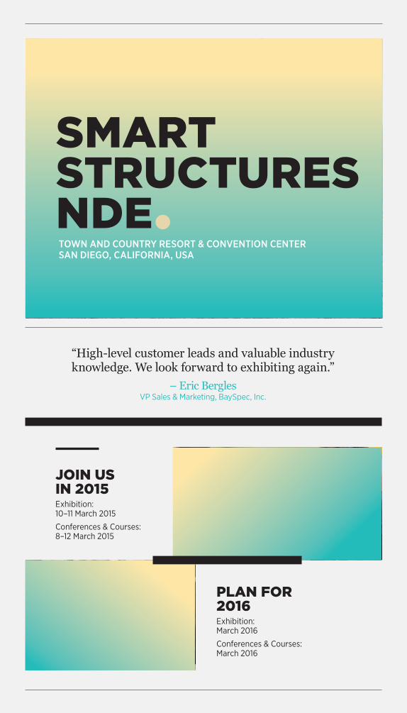
“High-level customer leads and valuable industry knowledge. We look forward to exhibiting again.”
– Eric Bergles VP Sales & Marketing, BaySpec, Inc.
SMART STRUCTURES NDE•
PLAN FOR 2016Exhibition: March 2016
Conferences & Courses: March 2016
JOIN US IN 2015Exhibition: 10–11 March 2015
Conferences & Courses: 8–12 March 2015
TOWN AND COUNTRY RESORT & CONVENTION CENTER SAN DIEGO, CALIFORNIA, USA

Connect and do business with researchers, developers, and integrators from funding agencies, academia, military, and industry by exhibiting where people gather to discuss “smart structures” and non-destructive evaluation – from aircraft to artificial muscles to civil infrastructure. If you sell components, devices, and systems for sensing, actuators and dampers, fiber sensors, sensor networks, testing equipment and instrumentation, or new materials for smart structures, you should show your offerings at SPIE Smart Structures/NDE.
This event has become the premier multidisciplinary forum where new possibilities are explored and new technologies discussed in relation to safety and reliability of structures and vehicles, bridges and buildings; biomimetics and robotics; sensors; multifunctional materials; NDE; and other structural monitoring technologies.
11
Connect one-on-one with a cross-disciplinary audience working on sensors, smart structures and non-destructive evaluation.
kEy METRICS800 Attendees
15 Exhibitors
900 Technical Papers
ATTENDEESStructural and mechanical engineers
Optical and materials engineers
Systems and reliability engineers
Fiber optic scientists
Mathematicians and educators
Systems integrators
CONFERENCE TOPICSAdaptive structures and mechanisms
Smart structures and vehicles
Actuators and damping
Biomimetics
Active materials
Embedded sensors
Sensor networks
Real-time NDE
Structural health monitoring
Fiber sensors
EXHIBITION TECHNOLOGIESStructural health monitoring
Civil infrastructure systems
Smart structures and materials
Automotive and aerospace applications
Actuators and damping
Nanotechnology
Modeling, control, and optimization
Energy harvesting/energy systems
Bio-inspired and robotic systems
Electroactive polymers
Shape memory alloys
MR fluids and elastomers
Piezoelectric materials
Embedded and self-diagnostic sensors
Optical fiber sensors
Sensor networks
Real-time NDE
Town and Country Resort & Convention Center San Diego, California, USA

PHOTONICS EUROPE•
BIENNIAL 2018 EVENT
JOIN US IN 2016Exhibition: 4–5 April 2016
Conferences: 3–7 April 2016
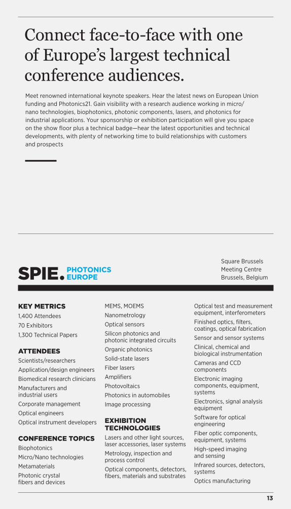
Meet renowned international keynote speakers. Hear the latest news on European Union funding and Photonics21. Gain visibility with a research audience working in micro/nano technologies, biophotonics, photonic components, lasers, and photonics for industrial applications. Your sponsorship or exhibition participation will give you space on the show floor plus a technical badge—hear the latest opportunities and technical developments, with plenty of networking time to build relationships with customers and prospects
13
Connect face-to-face with one of Europe’s largest technical conference audiences.
kEy METRICS1,400 Attendees
70 Exhibitors
1,300 Technical Papers
ATTENDEESScientists/researchers
Application/design engineers
Biomedical research clinicians
Manufacturers and industrial users
Corporate management
Optical engineers
Optical instrument developers
CONFERENCE TOPICSBiophotonics
Micro/Nano technologies
Metamaterials
Photonic crystal fibers and devices
MEMS, MOEMS
Nanometrology
Optical sensors
Silicon photonics and photonic integrated circuits
Organic photonics
Solid-state lasers
Fiber lasers
Amplifiers
Photovoltaics
Photonics in automobiles
Image processing
EXHIBITION TECHNOLOGIESLasers and other light sources, laser accessories, laser systems
Metrology, inspection and process control
Optical components, detectors, fibers, materials and substrates
Optical test and measurement equipment, interferometers
Finished optics, filters, coatings, optical fabrication
Sensor and sensor systems
Clinical, chemical and biological instrumentation
Cameras and CCD components
Electronic imaging components, equipment, systems
Electronics, signal analysis equipment
Software for optical engineering
Fiber optic components, equipment, systems
High-speed imaging and sensing
Infrared sources, detectors, systems
Optics manufacturing
Square Brussels Meeting Centre Brussels, Belgium

“A center of excellence for sensing and security technologies. We get to showcase our technologies to the right audience.”
– Colin Pearce Founder & CEO, Active Silicon Ltd.
DSS EXPO•
PLAN FOR 2016Exhibition: 19-21 April 2016
Conferences & Courses: 18-22 April 2016
JOIN US IN 2015Exhibition: 21–23 April 2015
Conferences & Courses: 20–24 April 2015

SPIE Defense, Security, and Sensing attracts more prospects for optics, sensors, and IR imaging equipment than anywhere in the world. More than 6,000 decision makers, researchers, and innovators come to learn, share ideas, and find new technologies and product solutions that help them meet challenging requirements.
Exhibit at SPIE Defense, Security, and Sensing and interact one-on-one with buyers from the world’s largest defense and security companies, research organizations, government departments, and sensing solution providers.
15
The East Coast’s largest exhibition on sensing and imaging technologies for defense, industrial, and commercial applications.
kEy METRICS6,000 Attendees
450 Exhibitors
2,200 Technical Papers
45 Courses
ATTENDEESCorporate management
Government/military purchasing managers
Applied and basic researchers
Design engineers
Product developers
Program managers
System integrators
CONFERENCE TOPICSInfrared sensors and systems
Hyperspectral imaging
Radar sensors
Pattern recognition
Laser technologies and systems
Next-generation sensors and systems
Displays, guidance, and navigation
Modeling, simulation, and visualization
Signal and image processing
Micro- and nanotechnology sensors
Sensing for agriculture and food/water safety
Sensor networks
Data mining
C3I, airborne reconnaissance, space and systems operations
Biometrics and aviation security
Forensic technologies
Unmanned vehicles
ISR/CBRNE
EXHIBITION TECHNOLOGIESInfrared sources, detectors, and systems
Chemical and biological sensing
Lasers and other light sources, laser accessories, and laser systems
Cameras and CCD components
Displays
Imaging components, equipment, and systems
Fiber optic components, equipment, and systems
Optical components including specialized lenses and coatings
High-speed imaging and sensing
High-precision optics manufacturing
Robotics
Law enforcement technology
Photonic sensors
Baltimore Convention Center Baltimore, Maryland, USA

ASTRONOMICAL TELESCOPES + INSTRUMENTATION•
PLAN FOR 2016Edinburgh UK
Exhibition: 28-29 June 2016
Conferences & Courses: 26 June-1 July 2016
BIENNIAL 2018 EVENT

17
SPIE Astronomical Telescopes + Instrumentation is a prestigious gathering of astronomical instrumentation experts from around the world, making it an ideal place to meet your customers and prospects. Develop new business at this SPIE conference that brings your target market together like no other event.
See over 2,200 attendees representing the largest international telescope projects. Join the directors, project managers, and systems engineers who build the world’s ground- and space-based telescopes at this extraordinary event. Make face-to-face contact with the broad range of component designers and suppliers that make this exhibition the leading forum for astronomical instrumentation.
The world’s premier gathering of astronomers and astronomical telescope and instrumentation developers.
kEy METRICS2,200 Attendees
90 Exhibitors
2,200 Technical Papers
12 Courses
ATTENDEESProject/program managers
Applied researchers
Engineers and designers
Systems engineers
CONFERENCE TOPICSTelescopes and systems
Space telescopes
Ground-based and airborne telescopes
Optical and IR interferometry
Adaptive optics systems
Observatory operations
Technology advancements
Optical and mechanical systems engineering
Detectors
Software and control
EXHIBITION TECHNOLOGIESGround instruments
Astronomy information technologies
Space telescopes and instruments
Detectors
Specialized optical materials
Precision manufacturing
Test and analysis systems
Adaptive optics
Lenses and mirrors
Edinburgh, UK
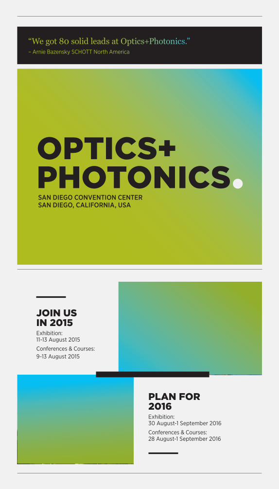
PLAN FOR 2016Exhibition: 30 August-1 September 2016
Conferences & Courses: 28 August-1 September 2016
JOIN US IN 2015Exhibition: 11-13 August 2015
Conferences & Courses: 9-13 August 2015
“We got 80 solid leads at Optics+Photonics.”– Arnie Bazensky SCHOTT North America
OPTICS+ PHOTONICS•SAN DIEGO CONVENTION CENTER SAN DIEGO, CALIFORNIA, USA

San Diego Convention Center San Diego, California, USA
With more work in emerging technologies presented at this conference than at any other, you can cost-effectively connect with technologists spanning nanoscience and engineering, solar energy, solid-state lighting, remote sensing, and optical engineering. You will have ample opportunities to connect with industry leaders and researchers who need new products to continue pushing the frontiers of discovery and application. Find your target audience and the connections you need at SPIE Optics + Photonics, held annually in San Diego.
19
Create new business at the largest multidisciplinary optics and photonics technical conference.
kEy METRICS4,500 Attendees
180 Exhibitors
3,000 Technical Papers
55 Courses
ATTENDEESApplication and product developers
Design engineers
Project managers
Applied researchers
Technical managers
Basic science researchers
Educators
Project leaders
CONFERENCE TOPICSOptical design
Advanced metrology
Remote sensing
Optical system design
Illumination engineering
Photovoltaics
Solar hydrogen
Thin film coatings
Solar concentrators
Plasmonics
Nanoengineered materials
Metamaterials
Nanocoatings
Nanomanufacturing
Organic photonics and electronics
OLEDs and LEDs
Photonics devices
Organic photovoltaics
Space optics
Nonlinear optics
x-ray optics
Astronomical optics
EXHIBITION TECHNOLOGIESOptical components
Detectors, sensors, and cameras
Lasers and accessories
Computer hardware and software
Imaging equipment
Test and analysis equipment
Optical fabrication and design services
Materials and chemicals
OLEDs and LEDs
Lenses
Fiber optics
Electronics and signal-analysis equipment
Displays
Positioning systems
Vibration-isolation equipment

“The main global event for mask manufacturers and their suppliers. It is the best place to meet the key
decision makers in the industry.”
– Frank Averdung President, Carl Zeiss SMT Inc., & Mng. Dir, Semiconductor Metrology Systems
PHOTOMASk TECHNOLOGy•
PLAN FOR 2016September 2016
JOIN US IN 2015Exhibition: 29–30 Sept. 2015
Conferences: 29 Sept.-1 Oct. 2015
21
kEy METRICS450 Attendees
20 Exhibitors
100 Technical Papers
ATTENDEESEngineers and designers
Corporate managers from the mask-making industry
Application and product developers
Experts in mask infrastructure and mask integration
People working in emerging mask technologies
Mask and chip designers
Resist chemists
Quality assurance specialists
CONFERENCE TOPICSPatterning
EUV
Immersion
Nanoimprint
Direct write
Data prep and management
OPC and phase-shift masks
Design and process integration
Design and data modeling
Defect inspection and repair
Mask yield and yield learning
Metrology
Maskless lithography
Materials
EXHIBITION TECHNOLOGIESElectron-beam lithography
EUV
Maskless
Metrology
Sources
Nanotechnology
Optical/laser microlithography
Resist technology and processing
Software
Electronic imaging components
Maintaining visibility with your customers helps you build your sales pipeline and sense changes in the market. Exhibit at SPIE Photomask Technology and be seen at the industry’s premier photomask meeting. Grow your business by cost-effectively connecting with the buyers and technical leaders who gather to discuss next-generation technology and new methods to lower costs and increase throughput.
Gain visibility at the mask industry’s top exhibition.
Monterey Conference Center and Monterey Marriott Monterey, California, USA
“This conference is critical for getting the core people together to have discussions. The exchange of technology
really helps us to innovate new technologies and that’s what we need with all these emerging markets.”
– Petrie Yam, KLA-Tencor

2015 OPTIFAB•
BIENNIAL 2017 EVENTConference & Exhibition: Fall of 2017
JOIN US IN 2015Exhibition: 13–15 October 2015
Conferences & Courses: 12–15 October 2015
The premier optical fabrication exhibition in North America

23
At SPIE Optifab, exhibitors showcase optical manufacturing technology, including equipment, machines, tools, materials, instrumentation, metrology, and processes. Optical fabrication solution providers come from across the world to demonstrate products and gain customers at SPIE Optifab.
Network with your customers, show your products, and grow revenue.
kEy METRICS1,800 Attendees
160 Exhibitors
10 Courses
90 Technical and Commercial Papers
ATTENDEE TOPICSMaterials scientists
Equipment operators
Optical engineers
Manufacturing and process engineers
Design and product developers
Corporate and manufacturing management
Purchasing/procurement agents
EXHIBITION TECHNOLOGIESOptical fabrication equipment
Optical components, materials, and systems
Optomechanical components and devices
Laser system components
Optical thin film coating
Optical metrology and testing equipment
Clean room equipment
Adhesives, glass, and consumables
Software for design, simulation, and testing
Metrology systems
Custom optics
Rochester Riverside Convention Center Rochester, New York, USA
“Exhibiting at Optifab is a very effective way to contact a large number of customers and vendors.”
—Michael Hartman SlicingTech
Reach two related audiences at Europe’s top security and defence event.
kEy METRICS900 Attendees (combined)
45 Exhibitors
SECURITy + DEFENCE CONFERENCE TOPICSSensors and sensor networks
Materials
Biological and chemical sensors and detectors
Optical devices
Signal processing
LIDAR
LADAR
SECURITy + DEFENCE EXHIBITION TECHNOLOGIESChemical and biological sensing
Infrared sources, detectors, and systems
Lasers and other light sources, laser accessories
Cameras and CCD components
Electronic imaging components, equipment, and systems
Fiber optic components, equipment, and systems
Optical components
High-speed imaging/sensing
Optics manufacturing
Nanotechnology
REMOTE SENSING CONFERENCE TOPICSUV, VIS and IR cameras and imaging systems
LIDAR, LADAR
Multi- and hyperspectral imaging
Adaptive optics
Image and signal processing
SECURITy+ DEFENCE•
Co-located with SPIE Remote Sensing Toulouse, France
SPIE Security + Defence attracts more than 400 attendees from 20 countries working in the European security and defence sector. Defence industry leaders from Europe and North America gather to share results and photonics technology developments.
SPIE Security + Defense is co-located with SPIE Remote Sensing, allowing access to two qualified groups of potential customers. SPIE Remote Sensing offers comprehensive coverage of scientific topics, applications, sensor systems, data analysis, and satellite platforms.
CONFERENCES: 21–25 SEPT. 2015 ExHIBITION: 22–23 SEPT. 2015

NORTH AMERICA
EUROPE
Exhibition Calendar.
10–11 February 2015 San Francisco, California, USA
28-29 June 2016Edinburgh, UKBiennial event
11–13 August 2015 August 2016 San Diego, California, USA
24–25 February 2015 23–24 February 2016 San Jose, California, USA
29-30 September 2015 September 2016 Monterey, California, USA
10-11 March 2015 March 2016 San Diego, California, USA
21–23 April 201519-21 April 2016 Baltimore, Maryland, USA
13–15 October 2015 Rochester, New York, USA Biennial event
25
4-5 April 2016 Brussels, Belgium
14–15 April 2015Prague, Czech RepublicBiennial event
www.spie.org/exhibitions
10–12 February 2015 16–18 February 2016 San Francisco, California, USA
7–8 February 2015 13–14 February 2016 San Francisco, California, USA
23–25 September 2015Toulouse, France2016 Europe - TBD
Contact SPIE Exhibition Sales to learn more
In America, Asia, UK, France, and the rest of the world
SPIE Headquarters Tel: +1 360 676 3290 [email protected] www.spie.org/exhibits
In Europe excluding UK, Ireland, and France
Hermann Doster Tel: +49 (0)7025/841 806 Mob: +49 (0)152/046 096 44 [email protected]

Non
-Pro
fit O
rg.
U.S.
Pos
tage
Paid
SPIE
P.O
. Box
10
Bel
lingh
am, W
A 9
8227
-00
10 U
SA
Reach your target marketwith SPIE Exhibitions.Plan now to exhibit in 2015/2016.
www.spie.org/exhibitions
MOVING TECHNOLOGY TO MARKET.