explanation of the problem - mcu turkey · t.c. dokuz eylÜl university department of computer...
TRANSCRIPT

T.C.DOKUZ EYLÜL UNIVERSITY
DEPARTMENT OF COMPUTER SCIENCE ENGINEERING
CPU-TURKEY
8-BIT COMPUTER
PROJECT KOJIKI
Ercan ŞAHAN
İzmir, 2008

KOJIKIDOCUMENTATION OF THE PROJECT
Table.1 ASC
Fetch : T0 : IRM[PC]Decode : T1 : D0…D7Decode IR(6…4)
ARIR(2…0), IIR(7), PCPC+1Indirect Addressing : D0’IT2 : ARM[AR]
Memory Reference :ADD : D1T3 : DRM[AR]
D1T4 : ACAC+DR, SC0, ECout, SC0AND : D2T3 : DRM[AR]
D2T4 : ACAC^DR, SC0LDA : D3T3 : DRM[AR]
D3T4 : ACDR, SC0STA D4T3 : M[AR]AC, SC0BUN : D5T3 : PCAR, SC0BSA : D6T3 : M[AR]PC, ARAR+1
D6T4 : PCAR, SC0ISZ : D7T3 : DRM[AR]
D7T4 : DRDR+1D7T5 : M[AR]DR, IF (DR = 0) THEN (PCPC+1), SC0
Register Reference :D0I’T4=r (Common to all register reference instructions.)Bi=IR(2…0), Decode (i = 0,1,2,…,7)
r : SC0SZE : rB0 : IF (E = 0) THEN (PCPC+1)CLA : rB1 : AC0SZA : rB2 : IF (AC = 0) THEN (PCPC+1)SNA : rB3 : IF (AC(3) = 1) THEN (PCPC+1)CMA : rB4 : ACAC’ (2’s Complement)ASHL : rB5 : ACASHL(AC), EAC(3)ASHR : rB6 : ACASHR(AC), EAC(0)INC : rB7 : ACAC+1
Input-Output :D0IT2=p (Common to all input-output instructions.)C=IR(2..0)
p : SC0INP : pC : ACINPUT
Stack Inst. :D0I=s (Common to all stack instructions.)Bi=IR(2..0) Decode (i = 1,2,3,4)
sT2 : SC0PUSH : sB1T2 : SPSP+1, DRAC
sB1T3 : M[SP]DRPOP : sB2T2 : DRM[SP]
sB2T3 : SPSP-1, ACDRSZEmpty : sB3T2 : IF (SP = 0) THEN (PCPC+1)SZFull : sB4T2 : IF (SP = 7) THEN (PCPC+1)
8-bit CPU Documentation CPU-Turkey 2

The table above is the table which simulates ASC computer. First, I have designed that table but after the design of the circuit according to that table, I have seen that some operations cause delays and these delays produce wrong outputs. I could not avoid from that problem, so I decided to change my Table which simulates ASC computer. The new table is below:
Table.2 ASC
Fetch : T0 : IRM[PC]Decode : T1 : D0…D7Decode IR(6…4)
ARIR(2…0), IIR(7), PCPC+1Indirect Addressing : D0’IT2 : ARM[AR]Memory Reference :
ADD : D1T3 : DRM[AR]D1T4 : ACAC+DR, SC0, ECout D1T5 : SC0
AND : D2T3 : DRM[AR]D2T4 : ACAC^DRD2T5 : SC0
LDA : D3T3 : DRM[AR]D3T4 : ACDRD3T5 : SC0
STA D4T3 : M[AR]ACD4T4 : SC0
BUN : D5T3 : PCARD5T4 : SC0
BSA : D6T3 : M[AR]PC, ARAR+1D6T4 : PCARD6T5 : SC0
ISZ : D7T3 : DRM[AR]D7T4 : DRDR+1D7T5 : M[AR]DR, IF (DR = 0) THEN (PCPC+1)D7T6 : SC0
Register Reference :D0I’T4=r (Common to all register reference instructions.)Bi=IR(2…0), Decode (i = 0,1,2,…,7)
SZE : rB0 : IF (E = 0) THEN (PCPC+1)CLA : rB1 : AC0SZA : rB2 : IF (AC = 0) THEN (PCPC+1)SNA : rB3 : IF (AC(3) = 1) THEN (PCPC+1)CMA : rB4 : ACAC’ (2’s Complement)ASHL : rB5 : ACASHL(AC), EAC(3)ASHR : rB6 : ACASHR(AC), EAC(0)INC : rB7 : ACAC+1
D0I’T5 : SC0Input-Output :
D0IT2=p (Common to all input-output instructions.)C=IR(2..0)
INP : pC : ACINPUTD0IT3 : SC0
Stack Inst. :D0I=s (Common to all stack instructions.)Bi=IR(2..0) Decode (i = 1,2,3,4)
PUSH : sB1T2 : SPSP+1, DRAC
8-bit CPU Documentation CPU-Turkey 3

sB1T3 : M[SP]DRPOP : sB2T2 : DRM[SP]
sB2T3 : SPSP-1, ACDRSZEmpty : sB3T2 : IF (SP = 0) THEN (PCPC+1)SZFull : sB4T2 : IF (SP = 7) THEN (PCPC+1)
sT4 : SC0
The second table has only one difference from the first table. The difference is the additional clocks in order to regulate the clear input for SC. If I don’t add these additional clocks, the operations do not work properly. The time for the operations are not enough for gaining the right result. SC is cleared just before the previous operation ends. By applying these changes I fixed timing problem for the computer ASC. And the design of the circuit is according to Table.2.
DESIGN TABLE OF THE REGISTER CONTROL UNIT
- CONTROL OF AC REGISTERD1T4+D2T4+D3T4+rB4+rB5+rB6+pC+sB2T3 (load)T4(D1+D2+D3)+r(B4+B5+B6)+pC+sB2T3 (load SIMPLIFIED)rB7 (increment)rB1 (clear)
- CONTROL OF DR REGISTERD1T3+D2T3+D3T3+D7T3+sB2T2+sB1T2T3(D1+D2+D3+D7)+sT2(B1+B2) (load SIMPLIFIED)D7T4 (increment)No clear
- CONTROL OF AR REGISTERT1+D0’IT2 (load)D6T3 (increment)No clear
- CONTROL OF IR REGISTERT0 (load)No incrementNo clear
- CONTROL OF SP REGISTERsB2T3 (load)sB1T2 (increment)sB2T3 (decrement)No clear
- CONTROL OF PC REGISTERD5T3+D6T4 (load)T1+(DR0+DR1+DR2+DR3)’(D7T5)+E’(rB0)+(AC0+AC1+AC2+AC3)’(rB2)+AC3(rB3)+(SP0+SP1+SP2+SP3)’(sB3T2)+(SP0SP1SP2SP3)(sB4T2) (inc)No clear.
- CONTROL OF SC REGISTERNo load.No increment.D1T4+D2T4+D3T4+D4T3+D5T3+D6T4+D7T5+r+p+sT2 (clear)T4(D1+D2+D3+D6)+T3(D4+D5)+D7T5+r+p+sT2 (clear SIMPLIFIED)
8-bit CPU Documentation CPU-Turkey 4

DESIGN TABLE OF THE ALU CONTROL UNIT
- ADDITION OPERATION CONTROLLERX1 = ADD(001) : D1T4
- AND OPERATION CONTROLLERX2 = AND(010) : D2T4
- TRANSFER(AC) OPERATION CONTROLLERX3 = TRA1(011) : D3T4+sB2T3
- 2’S COMPLEMENT OPERATION CONTROLLERX4 = CMP(100) : rB4
- A-SHIFT LEFT OPERATION CONTROLLERX5 = ASHL(101) : rB5
- A-SHIFT RIGHT OPERATION CONTROLLERX6 = SHR(110) : rB6
- TRANSFER(INPUT) OPERATION CONTROLLERX7 = TRA2(111) : pC
ALU SELECTIONS
S0 = X1+X3+X5+X7S1 = X2+X3+X6+X7S2 = X4+X5+X6+X7
DESIGN TABLE MEMORY SEGMENT CONTROL UNIT
- AR SELECTION(00) –DATA SEGMENT-M0 : D0’IT2+D1T3+D2T3+D3T3+D4T3+D6T3+D7T3+D7T5
D0’IT2+T3(D1+D2+D3+D4+D6+D7)+D7T5 (SIMPLIFIED)
- PC SELECTION(01) –CODE SEGMENT-M1 : T0
- SP SELECTION(10) –STACK SEGMENT-M2 : sB1T3+sB2T2
s(B1T3+B2T2) (SIMPLIFIED)
MEMORY SEGMENT SELECTIONS = S1S0
S0 = M1S1 = M2
DESIGN TABLE OF THE MEMORY UNIT
- CONTROL OF MEMORY (RAM)D4T3+D6T3+D7T5+sB1T3 (write enable)T3(D4+D6+sB1)+D7T5 (write enable SIMPLIFIED)
8-bit CPU Documentation CPU-Turkey 5

DESIGN TABLE OF THE BUS CONTROL UNIT
MEM 0AR 1 TO COMMON BUSSP 2 SELECTIONS: S2S1S0PC 3AC 4DR 5IR 6
- CONTROL OF MEMORYG0 : T0+D0’IT2+D1T3+D2T3+D3T3+D7T3+sB2T2
T0+T2(D0’I+sB2)+T3(D1+D2+D3+D7) (SIMPLIFIED)
- CONTROL OF AR REGISTERG1 : D5T3+D6T4
- CONTROL OF SP REGISTERG2 : sB2T3
- CONTROL OF PC REGISTERG3 : D6T3
- CONTROL OF AC REGISTERG4 : D4T3+sB1T2
- CONTROL OF DR REGISTERG5 : sB1T3+D7T5
- CONTROL OF IR REGISTERG6 : T1
BUS SELECTIONS
S0 = G1+G3+G5S1 = G2+G3+G6S2 = G4+G5+G6
8-bit CPU Documentation CPU-Turkey 6

CONTENTS OF THE MEMORY INITIALIZATION FILE “Memory.mif” IN BINARY FORMAT
-- MAX+plus II - generated Memory Initialization File
WIDTH = 8;DEPTH = 32;
ADDRESS_RADIX = HEX;DATA_RADIX = BIN;
CONTENT BEGIN00 : 11111111;01 : 11111111;02 : 11111111;03 : 11111111;04 : 11111111; DATA SEGMENT05 : 11111111;06 : 11111111;07 : 11111111;08 : 10000111;09 : 00000100;0A : 01000000;0B : 00000001;0C : 01000001;0D : 00000110;0E : 00000000;0F : 01011010;10 : 00110001; CODE SEGMENT11 : 10000001;12 : 00110001;13 : 00000111;14 : 01110000;15 : 01010100;16 : 10000010;17 : 00000110;18 : 11111111;19 : 11111111;1A : 11111111;1B : 11111111; STACK SEGMENT1C : 11111111;1D : 11111111;1E : 11111111;1F : 11111111;END;
CONTENTS OF THE MEMORY INITIALIZATION FILE “Memory.mif” IN SYMBOLIC FORMAT
08 : INP 1010 //Input can be modified…09 : CMA 0A : STA 00000B : CLA0C :Y = STA 00010D : ASHR0E : SZE0F : BUN X10 : LDA 000111 : PUSH1
12 :X = LDA 0001 13 : INC14 : ISZ 000015 : BUN Y16 : POP1
17 : ASHR
8-bit CPU Documentation CPU-Turkey 7

1-In my program I should have attached the instruction SZFull before the instruction PUSH and SZEmpty before the instruction POP in order to control the stack whether or not it is empty or full. But Code Segment was not enough to embed them.
After simulating the design in Altera, the waveform of the program, written above, is below. But unfortunately, I could not add the whole waveform. If I add the whole waveform the values are not seen well. Below, the waveform of the first repeat-until limb and the beginning of the second repeat-until limb are present.
clock = 100.0 nsinput = 1010 (can be modified by the user)
The output is not obvious on this waveform but the changes can be seen in the contents of the memory. The variable k, is shift right and controlled if E=0, then the original value is read from the memory and load to the AC Register.When the variable k is increases (0000, 0001, 0010, 0011,..-content1-), the value M, entered from the user, decreases (M is used as a counter…)
8-bit CPU Documentation CPU-Turkey 8

The scf above is only a part of the program. The full vision is below. The addresses 0 and 1 of the memory (data segment) are used as temporary register.
8-bit CPU Documentation CPU-Turkey 9

ALTERA DESIGNS OF THE COMPONENTS THAT ARE USED
8 BIT REGISTER
4 BIT REGISTER
8-bit CPU Documentation CPU-Turkey 10

3 BIT REGISTER
STACK POINTER
8-bit CPU Documentation CPU-Turkey 11

COMMON BUS
ALU
8-bit CPU Documentation CPU-Turkey 12

AND OPERATION
ADDITION OPERATION
8-bit CPU Documentation CPU-Turkey 13

ADDITION OF MEMORY ADDRESSES
TRANSFER OPERATION
8-bit CPU Documentation CPU-Turkey 14

2’S COMPLEMENT OPERATION
A-SHIFT (RIGHT-LEFT) OPERATION
8-bit CPU Documentation CPU-Turkey 15

ASC COMBINED CIRCUIT
REGISTER CONTROL UNIT
8-bit CPU Documentation CPU-Turkey 16

MEMORY CONTROL UNIT
BUS CONTROL UNIT
8-bit CPU Documentation CPU-Turkey 17

OPERATION CONTROL UNIT
r-p-s CONTROL UNIT(REGISTER – I/O CONTROLS)
8-bit CPU Documentation CPU-Turkey 18
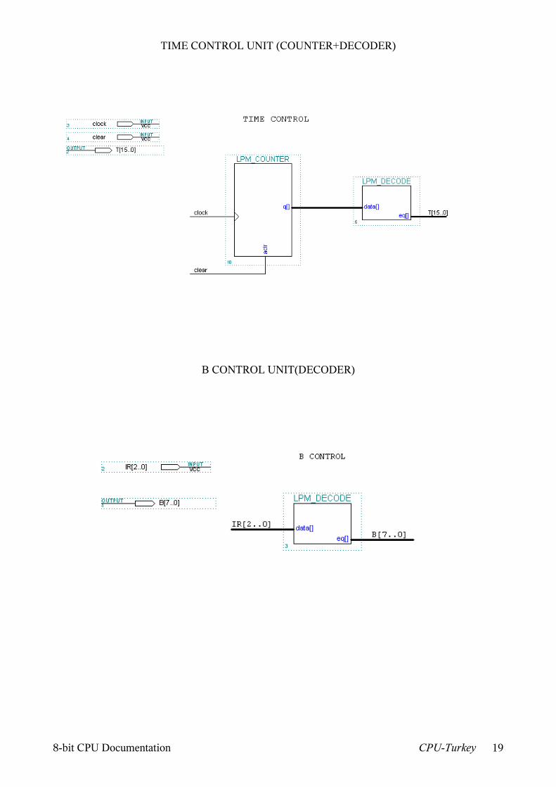
TIME CONTROL UNIT (COUNTER+DECODER)
B CONTROL UNIT(DECODER)
8-bit CPU Documentation CPU-Turkey 19

ALU CONTROL UNIT
FULL ADDER
8-bit CPU Documentation CPU-Turkey 20

SEGMENT SELECTION UNIT
MEMORY ADDRESS SELECTION
8-bit CPU Documentation CPU-Turkey 21

ALU – CONTROL UNIT – MEMORY – BUSES – REGISTERS COMBINED CIRCUIT
8-bit CPU Documentation CPU-Turkey 22