extrinsic evolution of the stacked gradient poly
TRANSCRIPT

9
Extrinsic Evolution of the Stacked Gradient Poly-Homojunction Photodiode Genre
Paul V. Jansz and Steven Hinckley Edith Cowan University
Australia
1. Introduction
The development of fast high-resolution CMOS imaging arrays, for application across a broad spectral range, requires suitable modifications to pixel architecture to improve individual photodiode quantum efficiency and crosstalk suppression (Furumiya et al., 2001; Brouk et al., 2003; Lee et al., 2003; Ghazi 2002). Presented in this chapter are the results of simulation studies that compare the detection efficacy of previous simulated photodiode architectures with the various configurations of the Stacked Gradient Poly-Homojunction (StaG) photodiode genre. The seed-idea that initiated this line of research, originated from a conference paper demonstrating the benefit of the StaG architecture to near infrared imaging (Dierickx & Bogaerts, 2004). The possibility of controlling photo-carrier direction, led to a radical “out-of-the-box” suggestion of improving the pixel’s response characteristics further, by concaving the StaG layers within each pixel, so as to “focus” carrier motion into the pixel’s space charge region (SCR). The closest structure to this that was possible to simulate was the first modification to the “flat” StaG architecture: the “U” shaped StaG with interpixel nested ridges (StaG-R). Both this and the concave StaG, having serious fabrication issues, led to further pixel modifications. The result: the evolution of the StaG photodiode genre; driven by the need to improve upon the photodiodes sensitivity and crosstalk suppression for particularly back illuminated pixels, but also for the front illumination mode. This process is “extrinsic” evolution, because the proactive motivations and ideas for device development originated external to the device itself. The present studies have been conducted using 50
μm pitch pixels in order to compare response with previously characterised photodiode
architectures. Research into 5 μm pitch StaG pixels is currently under development. Contemporary research into Camera-on-a-CMOS chip technology has been focused on frontwall-illuminated (FW) architectures, in which the Active Pixel Sensor (APS) and the signal processing circuitry are coplanar-integrated (Shcherback & Yaddid-Pecht, 2003). This architecture is disadvantaged in a number of ways, including the incompatibility of different CCD and CMOS processing technologies and low fill factor. These disadvantages can be overcome by adopting a backwall-illuminated (BW) mode. As well as maximizing the fill factor, back illumination allows the combination of different processing technologies for the two chips. Additionally, it is possible to tailor the spectral response of individual photodiodes, due to the indirect nature of the silicon absorption coefficient, which affects the electron-hole pair photogeneration profile (Hinckley et al., 2000). Back illuminated
www.intechopen.com

Advances in Photodiodes
182
CMOS pin ultra-thin (75 μm) photodiodes have found application in medical imaging, particularly making x-ray, high quality, real time imaging possible (Goushcha et al., 2007). However, compared to front illumination, the backwall orientation is disadvantaged in crosstalk, speed and quantum efficiency (QE) due to the distality of the photo generated carrier envelope to the SCR, resulting in diffusion dominated pixels (Jansz Drávetzky, 2003). These problems need to be overcome before back illuminated CMOS photodiode arrays present a serious challenge to the present mature front illuminated active pixel sensor market. Architectures predicted to reduce these problems for back illuminated sensors : 1. Control the direction of diffusion/drift of the photo-carriers towards the SCR, 2. Bring the SCR closer to the photo-carrier envelope near the pixel backwall by,
a. Thinning the pixel (Goushcha et al., 2007). b. Widening the SCR by,
i. Increasing the reverse bias to the PN junction, and ii. Decreasing the doping on the substrate side of the PN junction, or iii. Having no doping (intrinsic Silicon) between the P and N regions, making a
pin “junction” (Goushcha et al., 2007). c. Extending the higher doped well towards the back wall by,
i. Thinning a single deep well so it is also depleted while at the same time extending the SCR to the pixel backwall, frontwall and side boundaries (2B). This is for small pitch, deep or shallow pixels.
ii. Using a number of deep thin wells (polywells) across the pixel to extend the SCR to the pixel’s backwall, frontwall, side boundaries and between each well (2B). This is for large pitch, deep or shallow pixels. iii. Using an inverted “T” shaped well and appropriate doping regimes (2B) that deplete the thin well and the substrate adjacent to the back wall. 3. Incorporate some form of inter-pixel barrier to lateral crosstalk carrier transport by,
a. Incorporating a single or multiple pixel boundary trench isolation consisting of i. Higher doped semiconductor with the same dopant type as the substrate (Jansz-Drávetzky, 2003; Hinckley et al., 2007; Jansz et al., 2008; Jansz, 2003). ii. Higher doped semiconductor with opposite dopant type to the substrate iii. Insulators such as SiO2 (Jansz et al., 2008). b. Using a guard ring electrode (Hinckley et al., 2004; Jansz, 2003). c. Using a guard (double) junction photodiode (Hinckley et al., 2004). The present interest in the StaG photodiode architectural genre, stems simply from its ability to control the direction of diffusion/drift of photo-carriers. However, StaG incorporation in the photodiode architecture needs to go hand in hand with SCR proximity (2.) and crosstalk barrier incorporation (3.) so that the benefit of the StaG structure in improved speed, crosstalk and sensitivity may be realised.
2. Theory
There are two mechanisms of photo-carrier transport: drift and diffusion. For fast, sensitive and no crosstalk pixels, drift is preferred. Drift is the movement of the majority or minority carriers due to the applied bias field and has a maximum mean thermal velocity of approximately 107 cm.s-1 in silicon (Streetman et al., 2000). This movement is orders of magnitude faster than diffusion, which depends on carrier concentration gradient.
www.intechopen.com

Extrinsic Evolution of the Stacked Gradient Poly-Homojunction Photodiode Genre
183
Transport of photocarriers generated in the SCR is dominated by drift. A wide SCR, drift-dominated, pixel, demonstrates superior carrier capture efficiency as the pixel is swept of carriers faster. Such pixels show far better crosstalk suppression due to the increased efficiency of ‘claiming’ carriers generated in their borders. Subsequently, they show enhanced sensitivity and lower junction capacitance due to their wider SCR. The Width of the SCR of a PN junction is dependent mostly on the N or P doping each side of the junction, and the potential bias across the junction,
02 ( ) a d
a d
V V N NW
q N N
ε⎡ ⎤⎛ ⎞− += ⎢ ⎥⎜ ⎟⎜ ⎟⎢ ⎥⎝ ⎠⎣ ⎦ (1)
where Na and Nd are the dopent concentrations on the P side and the N side of the PN junction respectively. Also ε, q and V are the permittivity of Silicon (11.8 x 8.85 x 10-14 Fcm-1), electronic charge (1.60 x 10⁻¹⁹ C) and the external bias voltage, respectively. Due to the concentration gradient of holes and electrons on either side of PN junction, the SCR is generated, having a width W, and an internal equilibrium potential, V0, across the junction. The SCR width is more affected by lowering the substrate doping concentration than by increasing the reverse voltage bias. Typical SCR width for 2 volt reverse bias is 6 μm, constrained by a 1014 cm-3 doping minimum. Lowering the substrate doping to the intrinsic level, 1.5 x 1010 cm-3, (using an intrinsic substrate) can expand the SCR to more than 450 μm. For such PIN photodiodes, all photo-carriers are generated within the SCR, and as such are collected quickly and specific to their pixel of origin. Knowledge of the SCR width is needed to determine the best StaG position in the pixel cross section (Jansz & Hinckley, 2010). The homojunction that is of interest in this chapter, though not as aggressive in carrier collection as a PN homojunction, also relies on an inbuilt potential gradient to capture diffusing carriers and direct their motion towards the SCR. As such, it works in collaboration with the PN junction to better manage pixel carrier capture efficiency. This particular homojunction is characterised by a layering of epitaxially grown epilayers on a substrate of similar doping type (Fig. 1). These epilayers decrease in doping concentration from the substrate towards the pixel well or PN junction at the front of the pixel. As such they represent a poly-homojunction, which is stacked and having a doping concentration gradient: The Stacked Gradient poly-homojunction photodiode – the “StaG”. To explain the StaG dynamics, it is necessary to visualise the cross section of a conventional StaG photodiode pixel in Fig. 1. The epilayer doping concentration decrease towards the front wall, from 1018 cm-3 in the substrate to 1014 cm-3 in the uppermost epilayer. This direction of decreasing doping concentration towards the SCR produces a potential gradient that drives the minority carriers vertically towards the SCR. Fig. 2. illustrates this principle using a schematic energy band diagram of the StaG geometry in Fig. 1, developed from Singh (1994). On average, the direction of reflected carriers is normal to the StaG strata (Hinckley & Jansz, 2007). Carriers diffusing away from the SCR will be reflected back towards the SCR as the StaG structure acts as a minority carrier mirror. This results in increased pixel carrier capture efficiency, reducing crosstalk and increasing pixel sensitivity. The effects of device geometry on pixel response resolution were measured by the pixel’s sensitivity, defined as maximum quantum efficiency (QE) and the electrical crosstalk. The
quantum efficiency (η=QE) for an incident wavelength (λ), and radiant intensity (Popt) was calculated using,
www.intechopen.com

Advances in Photodiodes
184
( )opt
hcI
qPλη λ λ= (2)
where h is Planck’s constant, c is the speed of light, and q is the electronic charge. The
simulated electron, hole and total current (Iλ) quantum efficiency was calculated.
Fig. 1. Cross-section of the simulated front illuminated conventional Stacked Gradient Homojunction (StaG) Photodiode array (Hinckley & Jansz, 2007). The back illuminated array is illuminated upon the bottom surface of the array diagram.
Fig. 2. Energy band diagram schematic of an unbiased five p-epilayer homojunction photodiode, indicating the favourable direction of carrier drift (Hinckley & Jansz, 2007).
3. Method
Imaging arrays consist of repeating light detecting elements called pixels. In these simulation studies, each pixel was configured as a reverse biased vertical p-n junction photodiode. The crosstalk and maximum QE of the central pixel of the three pixel array, 160
μm long and 12 μm deep, having different StaG configurations, were simulated using SEMICAD DEVICE (version 1.2), a two dimensional finite-element simulator. Fig. 3 shows the initial simulated primitive conventional photodiode that began this line of simulation research (Hinckley et al., 2002).
www.intechopen.com

Extrinsic Evolution of the Stacked Gradient Poly-Homojunction Photodiode Genre
185
Fig. 3. Cross-section of the simulated front illuminated conventional photodiode array (Hinckley et al, 2002). The back illuminated array is illuminated from underneath.
This photodiode’s standard dimensions included a well depth (Jdepth) of 1 μm, and a
substrate thickness (Tdepth) of 12 μm. Each photodiode was reverse biased by 2 volts. More recent StaG-polywell hybrid studies (Jansz & Hinckley, 2010; Jansz, Hinckley & Wild, 2010) used 3 volts to compare to previous research (Ghazi et al., 2002). Transparent ohmic contacts were used on the well and substrate surfaces on the front side of the array. The device with identical structure was simulated using back illumination followed by front illumination. The array was scanned at 5 ┤m intervals along the array, typically using a simulated laser beam of 633 nm wavelength, 5 ┤m width and 0.1 ┤W power. The use of 633 nm is for comparison to previous photodiode pixels simulation studies. For the generic StaG and in present StaG-hybrid research, simulation studies have explored pixel response characteristics for ultra-violet to near infrared illumination. To quantify the electrical crosstalk so that comparison could be made between photodiode configurations, the “relative crosstalk” was calculated. This was defined as the normalized quantum efficiency (NQE) of the photocurrent registering at the central pixel’s image (well) electrode for illumination at the 50┤m position along the array (Fig. 1). The response resolution of each device was compared using their relative crosstalk and their maximum quantum efficiency (QE). Though pixel speed was not considered, since the simulated source was continuous not modulated, it is clear that there is a relationship between crosstalk suppression and the ability for a pixel to manage its carrier capture efficiency. The latter also impacts on a pixel’s speed of photo-carrier capture.
4. The StaG photodiode genre
The following section reports on the characteristic features and performance of each present member of the StaG photodiode genre in chronological order of simulated investigation. The simulated structure, results and discussion are treated separately for each member.
4.1 The Beginning – The “Flat” StaG Photodiode The “flat” StaG photodiode, designated “StaG” (Fig. 1), QE response, backwall (BW) and frontwall (FW) illuminated, was compared to the QE response of two doping versions of the conventional photodiode (Fig. 3) with the following doping (well/substrate) regimes. Both versions had the same well doping as the flat-StaG, 1017 cm-3. One version (17/15) had a substrate doping of 1015 cm-3 while the other (17/14) had an order of magnitude lower substrate doping of 1014 cm-3 (Hinckley & Jansz, 2005).
www.intechopen.com

Advances in Photodiodes
186
Fig. 4. Comparison of StaG (Fig. 1) and conventional single junction photodiode (Fig. 3) QE, for both back (BW) and front (FW) illuminated cases, as a function of laser position (µm), and 633 nm wavelength (Hinckley & Jansz 2005).
Clearly back and front illumination responses of the flat-StaG architecture is superior in crosstalk suppression and maximum QE (together denoted “response resolution”) than either of the standard photodiode configurations. Fig. 4 shows that the response resolution decreases according to the trend: StaG > conventional PD 17/14 > conventional PD 17/15.
4.1.1 StaG relative crosstalk and sensitivity dependence on wavelength Fig. 5A compares the relative crosstalk (normalized QE for illuminations at the pixel
boundary at the 50 µm position allong the array in Fig. 1) dependence on wavelength for the
same 12µm thick back and front illuminated StaG (Fig. 1) and conventional photodiodes
(PD) (Fig. 3). The PDs have a p-substrate doping of 1014 cm-3 (17/14) or 1015 cm-3 (17/15),
and an n-well doping of 1017 cm-3. Back illuminated relative crosstalk generally decreases
with increase in wavelength, because the absorption length increases. This generates more
carriers closer to the SCR, resulting in better pixel carrier capture efficiency. The reverse is
true for the front illuminated pixels (Hinckley & Jansz, 2005).
www.intechopen.com

Extrinsic Evolution of the Stacked Gradient Poly-Homojunction Photodiode Genre
187
Fig. 5. Relative crosstalk (A) and sensitivity (B) dependence on wavelength for StaG (Fig. 1) and conventional photodiode (PD) (Fig. 3) for 1017 cm-3 well doping and two p-substrate dopings : 1015 cm-3 (17/15) and 1014 cm-3 (17/14) for back (BW) and front (FW) illumination (Hinckley & Jansz, 2005).
Fig. 5B compares the sensitivity – maximum quantum efficiency (QE) – dependence on wavelength for the 12µm thick back and front illuminated StaG and conventional (PD) photodiodes. For both structures, the back (BW) and front (FW) illumination modes have similar maximum QE dependence on wavelength. The StaG shows a higher maximum QE in both modes compared to both conventional photodiodes (PD). The back illuminated StaG maximum QE is superior to the other geometries, for the depth
of well (1 μm). For the shorter absorption length illuminations (┣ < 700nm), minority hole generation in the well is significant in front illumination causing significant hole diffusion, suppressing sensitivity. Back illumination is absorbed away from the well so that sensitivity is not suppressed. Note that the lower-doped substrate Naked photodiode (Naked 17/14) enhances carrier capture by increasing the SCR, also enhancing StaG response.
4.1.2 StaG relative crosstalk dependence on epilayer thickness and wavelength Fig. 6A demonstrates that, though the StaG has a better response resolution than the photodiode without the StaG, even for the StaG, widening the epilayers increases the chance of lateral carrier diffusion, reducing the pixels carrier capture efficency: crosstalk increasing across the given wavelength band. For any given epilayer thickness, front illumination crosstalk increasing while back illumination slightly decreases, and both responses level off at the same wavelengths. The increase or decrease is proportional to the increase in absorption length with wavelength increase. This is due to Silicon being an indirect band gap semiconductor: as the wavelength increases, front and back illumination generates carriers further and closer to the SCR, respectively. For thicker pixels, more of the longer wavelength light is absorbed, thus the larger the wavelength at which the pixel saturates; for any longer wavelengths more light passes though the pixel without being absorbed.
AB
www.intechopen.com

Advances in Photodiodes
188
Fig. 6. StaG (Fig. 1) relative crosstalk (A) and sensitivity (B) dependence on wavelength and epilayer thickness of 1.5, 3 and 10 µm. (Hinckley & Jansz, 2005).
Fig. 6B demonstrates that the thinner the epilayers, the better the sensitivity (maximum QE)
for back illumination until a wavelength-saturation sensitivity switch-point. There are two
switch points: 650 and 900 nm. From 650 upwards, the most sensitive StaG geometry
switches from the thinnest pixel (1.5 μm epilayer) to the next thinnest pixel (3 μm). The latter
remains the most sensitive until 900nm, when the thickest pixel (10 μm) becomes the most
sensitive. For the longer wavelengths and thicker pixels, the light that otherwise would have
passed through a thinner pixel, now generates carriers in a larger pixel volume, increasing
its carrier capture and so benefiting sensitivity. Below 650 nm, the light absorption length in
silicon is less than the depth of the thinnest pixel (1.5 μm epilayers = 9 μm total pixel depth),
resulting in all of the illumination being absorbed and generating carriers in close proximity
to the SCR. The result: maximum sensitivity for both modes of illumination.
4.1.3 StaG crosstalk and sensitivity score table: comparing photodiodes Table 1 compares, for illumination at 633nm, the relative crosstalk and maximum QE of the
• StaG photodiode (Fig. 2) (Hinckley & Jansz, 2005).
• Conventional single-junction photodiode (SJPD) (Fig. 4); (Jansz-Drávetzky, 2003)
• The SJPD with 8┤m deep boundary trench isolation (BTI);
• The SJPD with guard-ring electrodes (Guard);
• An N+PN- guard junction photodiode (DJPD) with well, guard and substrate depth of 1
μm, 2 μm and 12μm respectively; with SJPD pixel pitch (Jansz-Drávetzky 2003).
www.intechopen.com

Extrinsic Evolution of the Stacked Gradient Poly-Homojunction Photodiode Genre
189
Photodiode Type
Back Illuminated
Crosstalk
Front Illuminated
Crosstalk
Back Illuminated
Maximum QE
Front Illuminated
Maximum QE
StaG 0.105 0.020 0.986 0.940
SJPD 0.260 0.096 0.933 0.915
BTI 0.269 0.096 0.952 0.994
Guard 0.069 0.010 0.134 0.436
DJPD 0.001 0.001 0.004 0.543
Table 1. Comparison of crosstalk and maximum QE of the StaG and previously simulated photodiode geometries, for 633 nm illumination (Hinckley & Jansz, 2005).
This embryonic StaG (Fig. 1), for illumination at 633 nm, is already superior in sensitivity to these other back illumination photodiodes. Sensitivity for front illumination is trumped by the SJPD-BTI geometry, while StaG sensitivity is second best. For back illumination, the carrier envelope falls within the StaG layers, which act as
minority carrier mirrors reflecting the carriers towards the SCR. For the SJPD, with or
without BTI, the same carrier envelope is not constrained by a StaG lamination or by the BTI
that extends only 8 μm into the pixel; 4 μm from the back wall. Carriers are then lost to
crosstalk or recombination, reducing sensitivity and increasing crosstalk for SJPD-BTI.
Alternatively the reverse is true for front illumination. For the SJPD-BTI, the carrier
envelope is now proximal to the SCR and constrained by the BTI. This results in it’s
sensitivity being enhance above that of the StaG response.
Considering the relative crosstalk, the StaG is superior to the SJPD with and without BTI. It
is inferior to the SJPD with guard-ring-electrode and guard-junction. However the guard
configurations work on the basis of selective capture of the outer part of the carrier envelope
by the guard electrode and junction. A much reduced envelope is captured, reducing
crosstalk, but also reducing sensitivity especially for back illumination. Alternatively, StaG
dynamics works on the basis of capturing and focusing towards the SCR as much of the
carrier envelope as possible, with benefit to crosstalk and sensitivity (response resolution).
Plots of the electric field strength show that the StaG configuration has greater electric field
strength and extent around the pixel well, which improves its carrier capture efficiency,
which again translates to improving pixel response resolution (Hinckley & Jansz, 2005)
4.1.4 StaG – the first step The advantage of the StaG configuration is that carrier diffusion direction is controllable.
This vertical directionality is controlled by the doping concentration gradient of the
substrate and epilayers. Carriers generated in any epilayer that diffuse towards the back of
the pixel will strike a higher doped stratum which will reflect them back into their parent
epilayer so that their net displacement will be in the direction of the decrease in doping
concentration. Though there will still be lateral diffusion, there will be less recombination of
carriers diffusing away from the surface, while pixel capture volume will increase.
In this section, StaG carrier vertical directionality is imposed on the system by the planar
epilayers and the direction of epilayer doping gradient. In the next section, this directional
control is extrapolated to include an additional StaG structure that gives additional benefit
to the pixel’s carrier capture efficency.
www.intechopen.com

Advances in Photodiodes
190
4.2 StaG with inter-pixel nested ridges Captalizing on the StaG control of carrier direction, the original seed idea was to concave the StaG epilayers so that the focal point of the epilayers would be within the SCR. It was hypothesised that this would focus additional carriers, primarily lateral crosstalk carriers, towards the SCR, benefiting the pixel’s carrier capture efficiency. The closest analogy to this 'StaG-concave‘ configuration that was able to be defined using the simulation tool, was the StaG with Inter-Pixel Nested Ridges (StaG-R). Fig. 7 shows the cross section of the simulated StaG-R tri-pixel array. The diagram is squashed laterally making the 1 ┤m lateral spacing between the vertical nested epilayer ridges appear much closer. This makes each ridge horizontal width, from the highest epilayer ridge down to the substrate ridge, 10, 8, 6, 4 and 2 ┤m respectively.
Fig. 7. Cross-section of the simulated Stacked Gradient Homojunction Photodiode array with 5 epilayer inter-pixel nested ridges (Hinckley & Jansz 2007).
Simulations at 633 nm, have shown that it is possible to enhance the StaG PD’s response resolution further by including a laterally stacked gradient homojunction in the form of inter-pixel nested ridges. These ridges extend from each epilayer, symetrically about the pixel‘s lateral boundaries, towards the frontwall of the photodiode: lower ridges nesting into upper ridges. The new hypothesis, an extention of the StaG-concave hypothesis, reasoned that by having both laterally and vertically stacked gradient homojunctions, two dimensional control of photo-carrier transport can be achieved: the vertical stacking reducing diffusion towards the backwall while the lateral stacking reducing lateral carrier diffusion; a primary source of crosstalk. Pixel carrier capture efficiency was enhanced as predicted, benefiting pixel response resolution (Hinckley & Jansz, 2007).
4.2.1 StaG-R relative crosstalk dependence on ridge height. Fig. 8 shows relative crosstalk dependence on ridge height, or more correctly, dependence on the extent of ridge nesting for 633 nm illumination. Ridge height refers to the height of the lowest ridge which extends upwards from the substrate (Fig. 7). Higher ridges may be of equal or lesser height than the substrate ridge, because of the proximity of the epilayer ridge to the frontwall and the vertical gaps between the tops of ridges being equal for a given ridge height. The effect of increasing ridge height on relative crosstalk (Fig. 8), for 633 nm back illumination, is to monotonically reduce crosstalk. For front illumination, crosstalk reduces even faster than back illumination, with ridge increase, except for the lower ridges.
www.intechopen.com

Extrinsic Evolution of the Stacked Gradient Poly-Homojunction Photodiode Genre
191
Fig. 9 shows a maximum of 80% (back illumination) to 95 % (front illumination) reduction in relative crosstalk. This is significant, demonstrating that the StaG-R configuration fulfills the predicted benefit to crosstalk reduction (Hinckley & Jansz, 2007).
Fig. 8. Relative crosstalk of StaG-R (Fig. 7) compared to the StaG (ridge height = 0) (Fig. 1) and the normal photodiode (ridge height = -1) (Fig. 3) at 633 nm (Hinckley & Jansz 2007).
Fig. 9. Percentage reduction of relative crosstalk for StaG-R compared to the StaG PD (ridge height = 0) as a function of ridge height, at 633 nm (Hinckley & Jansz, 2007).
www.intechopen.com

Advances in Photodiodes
192
The crosstalk for front illuminated StaG-R is above StaG for ridge heights less than 2┤m,
because the ridges are broader at the front wall (10 μm) and only one ridge thick, not yet
being nested. Front illumination at the 50 μm position generates a carrier envelope in the wider and higher doped ridges towards the front of the pixel. This allows the possibility of lateral crosstalk diffusion. However, if the width of the uppermost ridge was less than 5┤m,
2.5 μm either side of the 55 μm position along the array, the 5 μm wide beam front
illuminating at the 50 μm position (the defined position for the measure of relative crosstalk), would fall outside the ridges, in the StaG epilayers of the neighbouring pixel. Generated carriers would be reflected off the un-nested ridges, resulting in a reduction in the relative crosstalk compared to the StaG configuration. Alternatively, for back illumination, the carrier envelope falls outside the thinner shallower, un-nested ridges, which act as doped boundary trench isolation (effectively, bi-layer lateral StaGs) enhancing crosstalk reduction. However, back illumination shows a poorer reduction in crosstalk than front illumination, for the higher ridges, because the generated carrier envelope is now no longer as near the frontwall as for front illumination. It, therefore does not benefiting from the same degree of StaG nesting as front illumination.
4.2.2 StaG-R relative crosstalk dependence on ridge height. Relative crosstalk was also investigated for dependence on the lateral gap between ridges for 633 nm illumination. Fig. 10 shows the normalized QE of front (FW) and back (BW) illuminated StaG-R dependence on the lateral ridge gap thickness for illumination outside (40┤m & 50┤m positions) and inside (60┤m position) the central pixel (Fig. 7). The relative
Fig. 10. The normalized QE of Frontwall (FW) and Backwall (BW) illuminated StaG-R dependence on lateral inter-ridge gap thickness for 633 nm illumination outside (40┤m & 50┤m positions) and inside (60┤m position) the central pixel (Hinckley & Jansz, 2007).
www.intechopen.com

Extrinsic Evolution of the Stacked Gradient Poly-Homojunction Photodiode Genre
193
crosstalk is represented by the BW50 and FW50 curves. The ridge height (9┤m) and the outer ridge width (10┤m) were fixed, while the other ridge widths were varied by a constant amount producing a range of inter-ridge gaps from 0.1┤m to 1┤m. This means that the maximum doped central substrate ridge was the widest for the thinnest gap of 0.1┤m, and thinnest for the thickest gap of 1┤m. As the gap between adjacent ridges increased, the relative crosstalk reduced. This was because the central substrate ridge width was decreasing with increasing gap. As the gap increased, the illuminations close to, but outside the central pixel (i.e. BW50 & FW50), fell inside the central ridge or were channeled into the central ridge (BW case) to a lessening extent. Thus, fewer carriers were generated in or channeled into the central ridge. This reduced the relative crosstalk. The further the illumination position was from the pixel boundary (i.e. the 55┤m position along the array), the more the pixel response became independent of the gap thickness: illumination at the 40┤m (BW40, FW40) and 60┤m (BW60, FW60) positions were less affected by the variation in ridge gap size. At these positions the illumination fell outside the nested ridges effectively reflecting carriers away from the pixel (40 ┤m position) and into the pixel (60 ┤m position), affecting the QE accordingly (Fig. 10).
4.2.3 StaG-R sensitivity dependence on ridge height Sensitivity (maximum QE) dependence on ridge dimensions was also investigated for 633 nm illumination. Fig. 11 demonstrates the sensitivity dependence on ridge height for the StaG-R (Fig. 7) compared to the StaG (Fig. 1) and conventional photodiode (Fig. 3).
Fig. 11. Maximum electron (nQE) and total Quantum Efficiency (QE) dependence on ridge height, for StaG-R (Fig. 7), compared to the StaG PD (ridge = 0), (Fig. 1) and conventional PD (ridge = -1) (Fig. 3) for backwall (BW) and frontwall (FW) illumination at 633 nm (Hinckley & Jansz, 2007).
Noted is the 0.9 % improvement in sensitivity for the back illuminated StaG-R compared to
the StaG. Though, for front illumination, the maximum electron QE (Max nQE) for the StaG-
www.intechopen.com

Advances in Photodiodes
194
R was larger than for the StaG, the well minority hole QE (i.e. the difference between the
maximum nQE (FW max nQE) and the maximum total QE (FW max QE) in Fig. 11, was
greater than for the StaG, resulting in a lower (0.6%) total QE for the StaG-R. The contrast
between the back and front illuminated photodiode response was due to the distality of the
generated carrier envelope from the photodiode’s SCR, for back illumination. Fewer
diffusing minority holes were generated inside the well and more drifting electrons in the
region below the well, for back illumination.
4.2.4 StaG-R sensitivity dependence on inter-ridge gap size Fig. 12 shows the sensitivity of the StaG-R for maximum ridge height as a function of lateral
inter-ridge gap thickness. This was for back (BW) and front (FW) illumination inside the
central pixel, i.e. 60┤m position (BW60, FW60), 70┤m position (BW70, FW70) and maximum
QE (BW Max QE, FW Max QE). The ridge height (9┤m) and the outer ridge width (10┤m)
were fixed, while the other ridge widths were varied from 0.1┤m to 1┤m as in Fig. 10.
Fig. 12. The absolute QE of Frontwall (FW) and Backwall (BW) illuminated StaG-R dependence on lateral inter-ridge gap thickness for 633 nm illuminations inside (60┤m, 70┤m and maximum QE positions) the central pixel (Hinckley & Jansz 2007).
Illuminations falling outside the nested ridges (70┤m & Max QE) produced absolute QE
responses that were affected minimally by a variation in lateral inter-ridge gap thickness.
Here the carrier envelope is proximal to the outer layer of the nested ridges only. Any
changes within the nested ridges does not connect with the associated carrier envelope.
Noted is the decreasing trend for the closest illumination position (60┤m) which intersects
the nested ridge (Fig. 7). The thinner the gap between nested ridges the larger the potential
gradient (Fig. 3) and drift coefficient resulting in more carriers being reflected into the
pixel’s capture volume, resulting in greater QE for illumination at the 60 μm position.
www.intechopen.com

Extrinsic Evolution of the Stacked Gradient Poly-Homojunction Photodiode Genre
195
4.2.5 StaG-R crosstalk and sensitivity score table: comparing photodiodes Table 2 & 3 compare, for 633nm illumination, the relative crosstalk and maximum QE of the
• StaG photodiode (Fig. 2) (Hinckley & Jansz, 2005);
• Conventional single-junction photodiode (SJPD) (Fig. 4) (Jansz-Drávetzky, 2003);
• The SJPD with 8┤m deep double boundary trench isolation (DBTI) (Jansz, 2003);
• The SJPD with guard-ring electrodes (Guard) (Jansz-Drávetzky & Hinckley, 2004);
• The SJPD with guard-ring electrode and 8┤m deep DBTI (Guard-DBTI) (Jansz, 2003);
• An N+PN- guard junction photodiode (DJPD) with well, guard and substrate depth of 1
μm, 2 μm and 12μm respectively; with SJPD pixel pitch (Jansz-Drávetzky 2003).
Backwall Illumination Frontwall Illumination
Photodiode Type Relative Crosstalk (% QE) Photodiode Type
DJPD (NPN) 0.0012 1 x 10⁻⁵ DJPD (NPN)
StaG-R 0.65 0.020 StaG-R
Guard-DBTI 3.6 0.55 StaG
StaG 3.8 0.6 Guard-DBTI
Guard 4.1 0.9 Guard
DBTI 14.9 7.3 DBTI
SJPD 21.6 14.5 SJPD
Table 2. Relative crosstalk at 633 nm for StaG-R and other simulated photodiodes.
Back Illuminated Front Illuminated
Photodiode Type Maximum % QE -
Sensitivity Photodiode Type
StaG-R 99.5 99.4 DBTI
StaG 98.6 98.4 SJPD
DBTI 95.2 94.0 StaG
SJPD 92.1 93.5 StaG-R
Guard-DBTI 15.3 54.2 DJPD (N+PN)
Guard 13.4 45.9 Guard-DBTI
DJPD (N+PN) 0.444 43.6 Guard
Table 3. Sensitivity at 633 nm for StaG-R and other photodiodes (Hinckley & Jansz, 2007).
Comparing the relative crosstalk parameter, the StaG-R geometry is second only to the
double junction photodiode for both modes of illumination. This confirms the initial
hypothesis: By adding an extra StaG dimension to the control of carrier direction, normal to
the existing StaG’s vertical direction, will capture more lateral carriers -benefiting crosstalk
reduction.
Comparing the sensitivity, the StaG-R geometry back illuminated is the best. Again the initial hypothesis is vindicated: A second StaG layer, normal to the first will enhance
www.intechopen.com
Advances in Photodiodes
196
sensitivity. This is a significant result for back illumination applications. Though front illuminated StaG-R sensitivity is below the StaG sensitivity, the result is not significant and front illuminated StaG-R still shows significant crosstalk suppression upto 95% (Fig. 9). Further characterisation of the superiority of the StaG-R response resolution for illumination with other wavelength, similar to the StaG, 400 – 1200 nm, is required.
4.2.6 StaG-R – the next step. The results indicate that StaG-R response resolution can be improve further by:
• Increasing the degree of ridge nesting and to approximate a continous concentration gradient by increasing the number of StaG layers.
• Reducing the total and individual thickness of the StaG layers, so increasing the potential gradient and improving the drift coefficient.
• Reducing the nested ridge thickness by reducing the vertical gap between ridges, so again benefiting potential gradient and drift coefficient.
HOWEVER, the most obvious obstical to StaG-R’s or StaG-concave’s physical application is their complexity of fabrication: the ridge nesting and StaG concaving procedures are non-existant in industry. This hurdle has led to the next step in the evolution of the StaG genre.
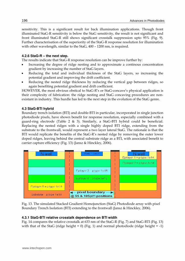
4.3 StaG-BTI hybrid Boundary trench isolation (BTI) and double-BTI in particular, incorporated in single junction photodiode pixels, have shown benefit for response resolution, especially combined with a guard-ring electrode (Table 2 & 3). Similarly, a StaG-BTI hybrid could be beneficial. Replacing the nested ridges with a single highly doped BTI ridge, extending from the substrate to the frontwall, would represent a two layer lateral StaG. The rationale is that the BTI would replicate the benefits of the StaG-R’s nested ridge by removing the outer lower doped ridges, leaving behind the central substrate ridge as a BTI, with associated benefit to carrier capture efficiency (Fig. 13) (Jansz & Hinckley, 2006).
Fig. 13. The simulated Stacked Gradient Homojunction (StaG) Photodiode array with pixel Boundary Trench Isolation (BTI) extending to the frontwall (Jansz & Hinckley, 2006).
4.3.1 StaG-BTI relative crosstalk dependence on BTI width Fig. 14 compares the relative crosstalk at 633 nm of the StaG-R (Fig. 7) and StaG-BTI (Fig. 13) with that of the StaG (ridge height = 0) (Fig. 1) and normal photodiode (ridge height = -1)
www.intechopen.com

Extrinsic Evolution of the Stacked Gradient Poly-Homojunction Photodiode Genre
197
(Fig 3). Here Fig. 8 results for StaG-R are superimposed on the StaG-BTI results for comparison. The horizontal scale is a dual scale for both StaG-R ridge height and BTI width.
Fig. 14. Relative crosstalk for 633 nm illumination, of StaG-R and StaG-BTI compared to StaG PD (BTI thickness = 0) and conventional photodiode (BTI thickness = -1) as a function of ridge height and BTI thickness (Jansz & Hinckley, 2006).
Comparing the lowest back illumination crosstalk percentage reduction below the StaG response, the StaG-R is significantly superior (80%) to the StaG-BTI (60%). The front illumination results are similar: StaG-R is moderately superior (95%) to the StaG-BTI (90%). The back illuminated StaG-BTI relative crosstalk increases for thicker BTI, because the illumination is proximal to the substrate, allowing carriers to diffuse laterally as well as channel more and more into a widening BTI. Conversly, the front illuminated StaG-BTI
relative crosstalk reduces up to 5 μm BTI width, because the illumination generates carriers in the StaG layers close to the frontwall where the higher doped BTI presents a barrier to
crosstalk; a barrier that improves with thickness. Larger than 5 μm BTI width, the illumination increasingly intersects the BTI in which generated carriers can increasingly channel as crosstalk as the BTI widens (Jansz & Hinckley, 2006).
4.3.2 StaG-BTI sensitivity dependence on BTI width Fig. 15 shows that the StaG-BTI is superior in sensitivity to the StaG-R, StaG and
conventional photodiodes. Back and front illuminated StaG-BTI have equivalent
sensitivities. Noted is the dramatic increase in sensitivity for the front illuminated StaG-BTI,
while the FW StaG-R drops in sensitivity below that of the FW StaG.
www.intechopen.com

Advances in Photodiodes
198
Fig. 15. Maximum quantum efficiency of StaG-R and StaG- BTI compared to StaG PD (ridge height/BTI thickness = 0) as a function of ridge height and BTI thickness (Jansz & Hinckley, 2006).
In Fig. 15, the front illuminated StaG-BTI maximum QE occurs just outside the well in the p-epilayer, while the StaG-R maximum QE occurs on the well wall, resulting in a higher minority hole diffusion current for the latter. Back illuminated StaG-BTI and StaG-R have their maximum sensitivity at the pixel centre (80┤m position) with photo-generation of minority hole diffusion current in the well marginally higher for the StaG-R, while their electron currents are similar.
4.3.3 StaG-BTI crosstalk and sensitivity score table: comparing photodiodes Using the previous Tables 2 and 3, StaG-BTI relative crosstalk and sensitivity can be compared to the other photodiodes. For relative crosstalk, StaG-BTI back and front illuminated is third best, just below StaG-R, in Table 2, at 1.4% and 0.042% QE, respectively. For sensitivity, StaG-BTI back and front illuminated is at to top of Table 3 at 99.8 % and 99.9% QE, respectively. Sensitivity is slightly superior to StaG-R because the substrate
doped BTI extends to the frontwall, while the central ridge for the StaG-R is 2 μm shorter.
4.3.4 StaG-BTI – The next step. Though the nested StaG ridges is still more effective as a minority carrier mirror, the StaG-
BTI is significantly less complex for fabrication. Though sensitivity is superior for the StaG-
BTI, the primary issue with its elevated crosstalk is the problem of carrier diffusion
channelling; a problem that is also present in the StaG-R. The main reason for this is that the
nested ridges and the BTI straddle the pixel boundary. Therefore any illumination in a
neighbouring pixel, next to the pixel boundary, will always intersect the BTI or nested ridge,
resulting in carrier diffusion channelling and its related crosstalk.
www.intechopen.com
Extrinsic Evolution of the Stacked Gradient Poly-Homojunction Photodiode Genre
199
The next step makes appropriate changes to the inter-pixel architecture so as to elliminate this pixel boundary straddle problem. Using insulator (SiO2) BTI is also explored.
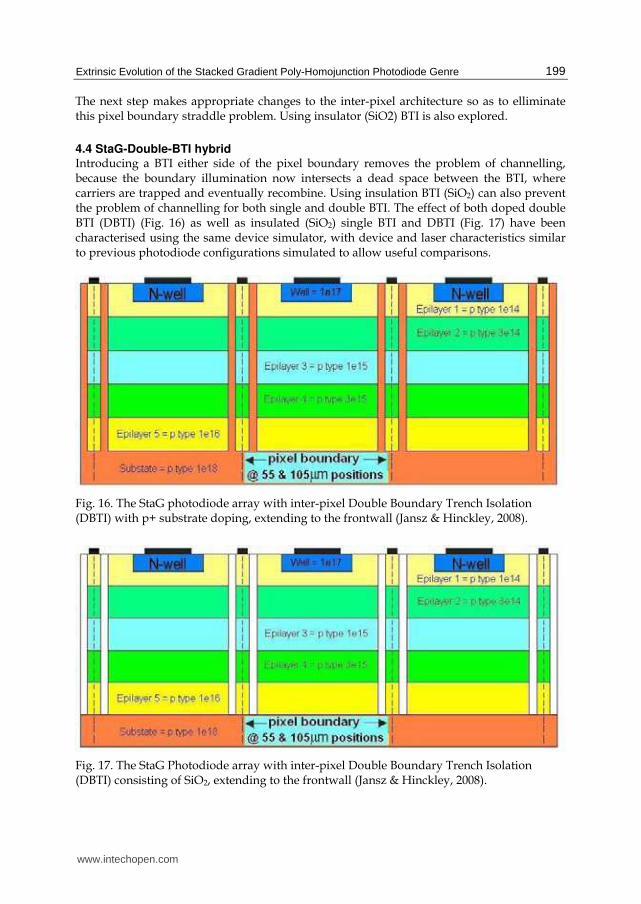
4.4 StaG-Double-BTI hybrid Introducing a BTI either side of the pixel boundary removes the problem of channelling, because the boundary illumination now intersects a dead space between the BTI, where carriers are trapped and eventually recombine. Using insulation BTI (SiO2) can also prevent the problem of channelling for both single and double BTI. The effect of both doped double BTI (DBTI) (Fig. 16) as well as insulated (SiO2) single BTI and DBTI (Fig. 17) have been characterised using the same device simulator, with device and laser characteristics similar to previous photodiode configurations simulated to allow useful comparisons.
Fig. 16. The StaG photodiode array with inter-pixel Double Boundary Trench Isolation (DBTI) with p+ substrate doping, extending to the frontwall (Jansz & Hinckley, 2008).
Fig. 17. The StaG Photodiode array with inter-pixel Double Boundary Trench Isolation (DBTI) consisting of SiO2, extending to the frontwall (Jansz & Hinckley, 2008).
www.intechopen.com

Advances in Photodiodes
200
4.4.1 Score table – graph legend: comparing photodiodes Table 4 contains the horizontal axis legend of the photodiode configurations (negative values) for Fig. 18 and Fig. 19. The positive values on the same axis refer to the doped DBTI widths in microns. “SJPD” refers to “single junction photodiode”.
Photodiode Configuration
Horizontal
axis number
(Fig 20 & 21)
BTI width (μm) for StaG Twin BTI 6 μm apart (Fig. 16) 1 - 5
Double Junction photodiode - 12 μm substrate (Jansz-Drávetzky, 2003) -1
StaG twin BTI SiO2 1 μm thick (Fig. 17) -2
StaG single BTI SiO2 1 μm thick (similar to Fig. 13) -3
StaG with maximum nested ridges (Fig. 7) -4
StaG single doped BTI 1 μm thick (Fig. 13) -5
StaG flat (Fig. 1) -6
SJPD with twin BTI SiO2 1 μm thick (Jansz, 2003; Jansz-Drávetzky, 2003) -7
SJPD with single BTI SiO2 1 μm thick (Jansz, 2003) -8
SJPD – convensional (Fig. 3) (Hinckley et al., 2002; Jansz-Drávetzky, 2003) -9
SJPD with Guard ring electrode and single BTI (Jansz, 2003) -10
SJPD with Guard ring electrode (Jansz-Drávetzky & Hinckley, 2004; Jansz-Drávetzky, 2003)
-11
Table 4. Horizontal axis number legend for Fig. 18 and Fig. 19.
4.4.2 StaG-DBTI crosstalk score table - graph: comparing photodiodes Crosstalk is superior for the hybids, SiO2 and doped Twin BTI StaG photodiodes compared
to all other photodiodes, except the Double Junction photodiode (DJPD) (Fig. 2), which also
shows retarded sensitivity. Frontwall crosstalk is below the backwall response. The physical
mechanism driving the reduction in crosstalk for DBTI StaG is internal reflection of carriers
generated in the neighbouring pixel and between the twin BTI (Jansz & Hinckley, 2008).
4.4.3 StaG-DBTI sensitivity score table - graph: comparing photodiodes Sensitivity (BW/FW) of StaG hybrids (99.8/99.8%) is above non-StaG geometries, including
the conventional photodiode (SJPD) (93/91%), the SJPD with guard ring electrode and BTI
(15/54%), SJPD and guard ring electrode only (13/46%) and the DJPD (0.004/54%). DJPD
sensitivity is reduced, especially for the backwall DJPD, as the majority of carriers are
generated outside the outer guard SCR (Jansz-Drávetzky, 2003).
www.intechopen.com

Extrinsic Evolution of the Stacked Gradient Poly-Homojunction Photodiode Genre
201
Fig. 18. Relative Crosstalk for Table 4 photodiodes.
www.intechopen.com

Advances in Photodiodes
202
Fig. 19. Maximum QE for Table 4 photodiodes.
5. Future trends for the StaG photodiode genre
One extrinsic evolutionary pressure driving improvement comes from the substrate’s
minimum doping constraint being only 1014 cm-3, resulting in insufficient SCR volume for
the primitive SJPD. If substrate doping could be ten times less, at 1013 cm-3, each 12 μm thick
pixel would be fully depleted with SCR widths of 14 – 21 μm for 1 – 3 volt reverse bias,
respectively. The result would be better photodiode response resolution than any of the
present doping constrained StaG hybrids. However, the StaG hybrids could also benefit
from a lowering of the doping constraint.
www.intechopen.com

Extrinsic Evolution of the Stacked Gradient Poly-Homojunction Photodiode Genre
203
Further characterisation of the latter StaG genre in terms of device response resolution for the wavelength range used to characterise the generic StaG photodiode is needed to understand the StaG’s response dependence on wavelength between 400 to 1200 nm. Other than 633 nm, other wavelengths are of interest due to niche applications or multi-wavelength specificity. Present research has (Jansz & Hinckley, 2010) and is investigating the suitability of application of the StaG-hybrid configuration to the poly-well geometry to realise back illuminated StaG-polywell photodiodes that have application to ultra-violet/blue sensing. The consideration at the beginning of this chapter, regarding architectures predicted to benefit back illuminated photodiode response resolution, has opened a number of research directions within the StaG genre as well as within the well-geometry photodiode genre.
6. Conclusion
This StaG genre explosion was sparked by a single idea: exploit the StaG ability to control carrier transport. It was along a path of device extrinsic evolution. This extrinsic pressure was proactive, rather than passive. It resulted in a process that aimed to achieve photodiode architectures that balanced the maximization of response resolution with the minimization of device fabrication complexity. This process has produced a time sequence of individual creations, through simulations, starting with the conventional vertical single junction photodiode (SJPD) with just well and substrate (Fig. 3). From this prototype, various branches have emerged. So far, these branches have form into a penta-dactile tree structure of vertical SJPD genre: Guard ring electrode SJPD, BTI-SJPD, Guard junction SJPD (DJPD), StaG-SJPD and Polywell SJPD. This development was driven primarily by the need to improve on the backwall illumination CMOS photodiode response, because of its advantages over the frontwall illumination mode. However, most of the improvements also benefit frontwall illuminated CMOS photodiodes across a broad spectrum. The present results indicate the prospect of obtaining significant crosstalk suppression and sensitivity enhancement in CMOS imaging arrays through achievable modifications to the array structure with the view to producing high-speed high-resolution imaging systems. Research in progress is investigating other StaG hybrids, as well as scaling effects down to
5μm pixel pitch on the benefits of these and other photodiode genre still to be exploited.
7. References
Brouk, I.; Nemirovsky, Y.; Lachowicz, S.; Gluszak, E.A.; Hinckley, S.; Eshraghian, K. (2003). Characterization of crosstalk between CMOS photodiodes. Solid State Electronics, 46, 53-6.
Dierickx, B. & Bogaerts, J. (2004). NIR-enhanced image sensor using multiple epitaxial layers. Proceedings of SPIE – IS&T Electronic Imaging, 5301, pp. 205–212.
Furumiya, M.; Ohkubo, H.; Muramatsu, Y.; Kurosawa, S.; Okamoto, F.; Fujimoto, Y.; Nakashiba, Y. (2001). High-sensitivity and no-crosstalk pixel technology for embedded CMOS image sensor. IEEE Transaction on Electron Devices, 48, 2221 - 6.
Ghazi, A.; Zimmermann, H. & Seegebrecht, P. (2002) CMOS photodiode with enhanced responsivity for the UV/Blue spectral range, IEEE Trans. Electron Devices, vol. 49, pp. 1124 – 8.
Goushcha, I.; Tabbert, B.; Popp, A.; Goushcha, A.O. (2007). Photodetectors based on back-illuminated silicon photodiode arrays for x-ray image systems. IEEE Sensors Applications Symposium (SAS), pp1 – 6, San Diego, California USA, 6 – 8 Feb.
www.intechopen.com

Advances in Photodiodes
204
Hinckley, S.; Gluszak, E.A.; Eshraghian, K. (2000). Modelling of device structural effects in backside illuminated CMOS compatible photodiodes. Proc. of Conference on Optoelectronic and Microelectronic Materials and Devices (COMMAD), pp 399 – 402, Melbourne. IEEE Press.
Hinckley, S.; Jansz, P.V.; Gluszak, E.A. & Eshraghian, K. (2002). Modelling of device structure effects on electrical crosstalk in back illuminated CMOS compatible photodiodes, Proc. of Conference on Optoelectronic and Microelectronic Materials and Devices (COMMAD), pp 397 – 400, Melbourne. IEEE Press.
Hinckley, S.; Jansz, P. V. & Eshraghian, K. (2004) Pixel structural effects on crosstalk in backwall illuminated CMOS compatible photodiode arrays. Proc. of DELTA 2004 Conference. pp 53 - 6, Melbourne, IEEE Press.
Hinckley, S. & Jansz P.V. (2005) “Stacked homojunction effects on crosstalk and response resolution in CMOS compatible photodiode arrays.”, Proc. Of IFIP WG 10.5 conference on VLSI-System on a Chip (VLSI-SoC 2005), Perth, IFIP, pp. 383-388.
Hinckley, S. & Jansz, P.V. (2007) The effect of inter-pixel nested ridges incorporated in a stacked gradient homojunction photodiode architecture. Proc. of SPIE Conference on Smart Structures, Devices and Systems III, pp 64141T-1 – 12, ISBN: 9780819465221, Adelaide, Dec. 2006, SPIE, Bellingham, Washington State USA.
Jansz P. V. (2003) Pixel boundary trench effects on a CMOS compatible single junction photodiode array, with and without guard-ring electrodes, pp 1 – 4, unpublished.
Jansz-Drávetzky, P.V. & Hinckley, S. (2004). Guard-ring electrode effects on crosstalk in simulated 2D CMOS compatible verticle photodiode pixel arrays. Proc. of Conference on Optoelectronic and Microelectronic Materials and Devices (COMMAD), pp 299 – 302. Melbourne, IEEE press, New Jersey, USA.
Jansz, P.V. & Hinckley, S. (2006) Inter-pixel boundary trench isolation effects on a stacked gradient homojunction single junction photodiode pixel architecture. Proc. of Conference on Optoelectronic and Microelectronic Materials and Devices (COMMAD2006), Melbourne. IEEE Press, New Jersey, USA.
Jansz, P.V. & Hinckley, S. (2008) Double boundary trench isolation effects on a stacked gradient homojunction photodiode array. Proc. of Conference on Optoelectronic and Microelectronic Materials and Devices (COMMAD), pp 156 – 9, ISBN: 9781424427178, Sydney, July 2008, IEEE press, New Jersey, USA.
Jansz, P.V. & Hinckley, S. (2010) Characterisation of a hybrid polywell and stacked gradient poly-homojunction CMOS photodiode. Proc. of Conference on Optoelectronic and Microelectronic Materials and Devices (COMMAD), Canberra, Dec. 2010, in press.
Jansz, P.V., Hinckley, S. & Wild, G. (2010) Effect of a polywell geometry on a CMOS photodiode array. 23rd IEEE International System On a Chip Conference (SOCC), Las Vegas, Sept. 2010, in press.
Jansz-Drávetzky, P. V. (2003) Device structural effects on electrical crosstalk in backwall illuminated CMOS compatible photodiode arrays. Honours Thesis. Edith Cowan University. Perth, Western Australia.
Lee, J.S.; Jernigan, M.E.; Hornsey, R.I. (2003). Characterization and deblurring of lateral crosstalk in CMOS image sensors, IEEE Transaction on Electron Devices, 50, 2361 - 8.
Shcherback, I. & Yaddid-Pecht O. (2003) Photoresponse analysis and pixel shape optimization for CMOS active pixel sensors. IEEE Transaction on Electron Devices, 50(1), 12 - 8.
Singh, J. (1994). Semiconductor Devices: An Introduction. McGraw-Hill, New York. Streetman, B. G. & Banerjee, S. (2000) Solid state electronic devices. Prentice Hall, ISBN: 0-13-
026101-7, New Jersey, 5th edition.
www.intechopen.com

Advances in PhotodiodesEdited by Prof. Gian Franco Dalla Betta
ISBN 978-953-307-163-3Hard cover, 466 pagesPublisher InTechPublished online 22, March, 2011Published in print edition March, 2011
InTech EuropeUniversity Campus STeP Ri Slavka Krautzeka 83/A 51000 Rijeka, Croatia Phone: +385 (51) 770 447 Fax: +385 (51) 686 166www.intechopen.com
InTech ChinaUnit 405, Office Block, Hotel Equatorial Shanghai No.65, Yan An Road (West), Shanghai, 200040, China
Phone: +86-21-62489820 Fax: +86-21-62489821
Photodiodes, the simplest but most versatile optoelectronic devices, are currently used in a variety ofapplications, including vision systems, optical interconnects, optical storage systems, photometry, particlephysics, medical imaging, etc. Advances in Photodiodes addresses the state-of-the-art, latest developmentsand new trends in the field, covering theoretical aspects, design and simulation issues, processing techniques,experimental results, and applications. Written by internationally renowned experts, with contributions fromuniversities, research institutes and industries, the book is a valuable reference tool for students, scientists,engineers, and researchers.
How to referenceIn order to correctly reference this scholarly work, feel free to copy and paste the following:
Paul V. Jansz and Steven Hinckley (2011). Extrinsic Evolution of the Stacked Gradient Poly-HomojunctionPhotodiode Genre, Advances in Photodiodes, Prof. Gian Franco Dalla Betta (Ed.), ISBN: 978-953-307-163-3,InTech, Available from: http://www.intechopen.com/books/advances-in-photodiodes/extrinsic-evolution-of-the-stacked-gradient-poly-homojunction-photodiode-genre

© 2011 The Author(s). Licensee IntechOpen. This chapter is distributedunder the terms of the Creative Commons Attribution-NonCommercial-ShareAlike-3.0 License, which permits use, distribution and reproduction fornon-commercial purposes, provided the original is properly cited andderivative works building on this content are distributed under the samelicense.