f mc-16lx mb90335 series mb90337/f337/v330a · • dtp/external interrupt circuit (8 channels) •...
TRANSCRIPT
DS07-13735-1EFUJITSU SEMICONDUCTORDATA SHEET
16-bit Proprietary MicrocontrollerCMOS
F2MC-16LX MB90335 Series
MB90337/F337/V330A DESCRIPTION
The MB90335 series are 16-bit microcontrollers designed for applications, such as personal computer peripheraldevices, that require USB communications. The USB feature supports not only 12-Mbps Function operation butalso Mini-HOST operation. It is equipped with functions that are suitable for personal computer peripheral devicessuch as displays and audio devices, and control of mobile devices that support USB communications. Whileinheriting the AT architecture of the F2MC* family, the instruction set supports the C language and extendedaddressing modes and contains enhanced signed multiplication and division instructions as well as a substantialcollection of improved bit manipulation instructions. In addition, long word processing is now available by intro-ducing a 32-bit accumulator.
* : F2MC stands for FUJITSU Flexible Microcontroller, a registered trademark of FUJITSU LIMITED.
FEATURES• Clock
• Built-in oscillation circuit and PLL clock frequency multiplication circuit• Oscillation clock• The main clock is the oscillation clock divided into 2 (for oscillation 6 MHz : 3 MHz) • Clock for USB is 48 MHz• Machine clock frequency of 6 MHz, 12 MHz or 24 MHz selectable• Minimum execution time of instruction : 41.6 ns (6 MHz oscillation clock, 4-time multiplied : machine clock
24 MHz and at operating VCC = 3.3 V)
• The maximum memory space:16 MB• 24-bit addressing• Bank addressing
(Continued)
PACKAGE
64-pin plastic LQFP
(FPT-64P-M09)
MB90335 Series
2
(Continued)
• Instruction system• Data types: Bit, Byte, Word, Long word • Addressing mode (23 types) • Enhanced high-precision computing with 32-bit accumulator• Enhanced Multiply/Divide instructions with sign and the RETI instruction
• Instruction system compatible with high-level language (C language) and multi-task• Employing system stack pointer• Instruction set symmetry and barrel shift instructions
• Program Patch Function (2 address pointer)
• 4-byte instruction queue
• Interrupt function• Priority levels are programmable• 20 interrupts function
• Data transfer function• Extended intelligent I/O service function (EI2OS) : Maximum of 16 channels• µDMAC : Maximum 16 channels
• Low Power Consumption Mode• Sleep mode (with the CPU operating clock stopped) • Time-base timer mode (with the oscillator clock and time - base timer operating)• Stop mode (with the oscillator clock stopped)• CPU intermittent operation mode (with the CPU operating at fixed intervals of set cycles)
• Package• LQFP-64P (FPT-64P-M09 : 0.65 mm pin pitch)
• Process : CMOS technology
• Operation guaranteed temperature: −40 °C to +85 °C (0 °C to +70 °C when USB is in use)
MB90335 Series
INTERNAL PERIPHERAL FUNCTION (RESOURCE)• I/O port: Max 45 ports
• Time-base timer : 1channel
• Watchdog timer : 1 channel
• 16-bit reload timer : 1 channel
• Multi-functional timer• 8/16-bit PPG timer (8-bit × 4 channels or 16-bit × 2 channels) the period and duty of the output pulse can be
set by the program.• 16-bit PWC timer : 1 channel
Timer function and pulse width measurement function
• UART : 2 channels• Equipped with Full duplex double buffer with 8-bit length• Asynchronous transfer or clock-synchronous serial (I/O extended serial) transfer can be set.
• Extended I/O serial interface: 1 channel
• DTP/External interrupt circuit (8 channels)• Activate the extended intelligent I/O service by external interrupt input• Interrupt output by external interrupt input
• Delayed interrupt output module• Output an interrupt request for task switching
• USB : 1 channel• USB function (conform to USB 2.0 Full Speed) • Full Speed is supported/Endpoint are specifiable up to six.• Dual port RAM (The FIFO mode is supported).• Transfer type: Control, Interrupt, Bulk or Isochronous transfer possible• USB Mini-HOST function
• I2C* Interface : 1 channel• Supports Intel SM bus standards and Phillips I2C bus standards• Two-wire data transfer protocol specification• Master and slave transmission/reception
* : I2C license : Purchase of Fujitsu I2C components conveys a license under the Philips I2C Patent Rights to use, these components in an I2C system provided that the system conforms to the I2C Standard Specification as defined by Phillips.
3
MB90335 Series
4
PRODUCT LINEUP
* : It is setting of Jumper switch (TOOL VCC) when Emulator (MB2147-01) is used. Please refer to the MB2147-01 or MB2147-20 hardware manual (3.3 Emulator-dedicated Power Supply Switching) about details.
PACKAGES AND PRODUCT MODELS
: Yes × : No
Part number MB90V330A MB90F337 MB90337
Type For evaluation Built-in Flash Memory Built-in Mask ROM
ROM capacity No 64 KB
RAM capacity 28 KB 4 KB
Emulator-specific power supply *
Used bit ⎯
CPU functions
Number of basic instructionsMinimum instruction execu-tion timeAddressing typeProgram Patch FunctionMaximum memory space
: 351 instructions : 41.6 ns / at oscillation of 6 MHz
(When 4 times are used : Machine clock of 24 MHz) : 23 types : For 2 address pointers : 16 MB
Ports I/O Ports(CMOS) 45 ports
UART
Equipped with full-duplex double bufferClock synchronous or asynchronous operation selectable.It can also be used for I/O serial.Built-in special baud-rate generatorBuilt-in 2 channels
16-bit reload timer16-bit reload timer operationBuilt-in 1 channel
Multi-functional timer8/16-bit PPG timer (8-bit mode × 4 channels, 16-bit mode × 2 channels) 16-bit PWC timer × 1 channel
DTP/External interrupt8 channelsInterrupt factor : “L”→“H” edge /“H”→“L” edge /“L” level /“H” level selectable
I2C 1 channel
Extended I/O serial interface 1 channel
USB1 channelUSB function (conform to USB 2.0 Full Speed) USB Mini-HOST function
Withstand voltage of 5 V 8 ports (Excluding VBUS and I/O for I2C)
Low Power Consumption Mode
Sleep mode/Timebase timer mode/Stop mode/CPU intermittent mode
Process CMOS
Operating voltage VCC 3.3 V ± 0.3 V (at maximum machine clock 24 MHz)
Package MB90337 MB90F337 MB90V330A
FPT-64P-M09 (LQFP-0.65 mm) ×
PGA-299C-A01 (PGA) × ×
MB90335 Series
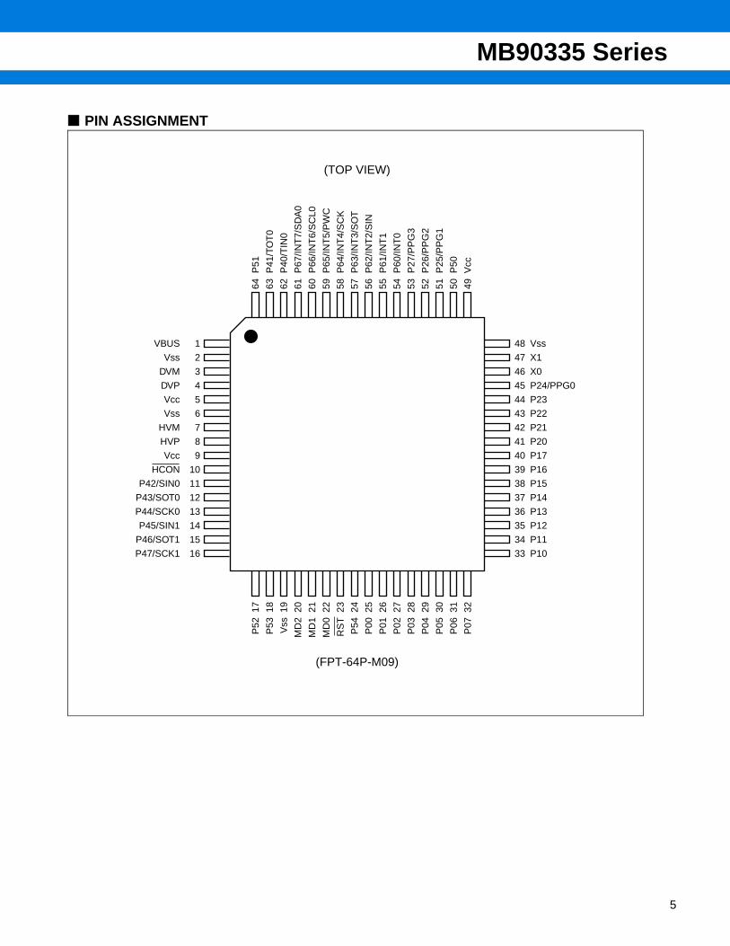
PIN ASSIGNMENT
(TOP VIEW)
(FPT-64P-M09)
VBUS
Vss
DVM
DVP
Vcc
Vss
HVM
HVP
Vcc
HCON
P42/SIN0
P43/SOT0
P44/SCK0
P45/SIN1
P46/SOT1
P47/SCK1
1
2
3
4
5
6
7
8
9
10
11
12
13
14
15
16
48
47
46
45
44
43
42
41
40
39
38
37
36
35
34
33
Vss
X1
X0
P24/PPG0
P23
P22
P21
P20
P17
P16
P15
P14
P13
P12
P11
P10
64 63 62 61 60 59 58 57 56 55 54 53 52 51 50 49
P51
P41
/TO
T0
P40
/TIN
0
P67
/INT
7/S
DA
0
P66
/INT
6/S
CL0
P65
/INT
5/P
WC
P64
/INT
4/S
CK
P63
/INT
3/S
OT
P62
/INT
2/S
IN
P61
/INT
1
P60
/INT
0
P27
/PP
G3
P26
/PP
G2
P25
/PP
G1
P50
Vcc
17 18 19 20 21 22 23 24 25 26 27 28 29 30 31 32
P52
P53 Vss
MD
2
MD
1
MD
0
RS
T
P54
P00
P01
P02
P03
P04
P05
P06
P07
5
MB90335 Series
6
PIN DESCRIPTION
* : For circuit information, see “ I/O CIRCUIT TYPE”.(Continued)
Pin no.Pin name Circuit
type*
Status at reset/
functionFunction
QFPM09
46 , 47 X0, X1 AOscillation
status
It is a terminal which connects the oscillator.When connecting an external clock, leave the X1 pin side uncon-nected.
23 RST F Reset input External reset input pin.
25 to 32 P00 to P07 I
Port input (High-Z)
General purpose input/output port.The ports can be set to be added with a pull-up resistor (RD00 to RD07 = 1) by the pull-up resistor setting register (RDR0). (When the power output is set, it is invalid.)
33 to 40 P10 to P17 I
General purpose input/output port.The ports can be set to be added with a pull-up resistor (RD10 to RD17 = 1) by the pull-up resistor setting register (RDR1). (When the power output is set, it is invalid.)
41 to 44 P20 to P23 D General purpose input/output port.
45P24
DGeneral purpose input/output port.
PPG0 Functions as output pins of PPG timers ch0.
51 to 53 P25 to P27
DGeneral purpose input/output port.
PPG1 to PPG3
Functions as output pins of PPG timers ch1 to ch3.
62P40
HGeneral purpose input/output port.
TIN0 Function as event input pin of 16-bit reload timer.
63P41
HGeneral purpose input/output port.
TOT0 Function as output pin of 16-bit reload timer.
11P42
HGeneral purpose input/output port.
SIN0 Functions as a data input pin for UART ch0.
12P43
HGeneral purpose input/output port.
SOT0 Functions as a data output pin for UART ch0.
13P44
HGeneral purpose input/output port.
SCK0 Functions as a clock I/O pin for UART ch0.
14P45
HGeneral purpose input/output port.
SIN1 Functions as a data input pin for UART ch1.
15P46
HGeneral purpose input/output port.
SOT1 Functions as a data output pin for UART ch1.
16P47
HGeneral purpose input/output port.
SCK1 Functions as a clock I/O pin for UART ch1.
50 P50 K General purpose input/output port.
64 P51 K General purpose input/output port.
17, 18 P52, P53 K General purpose input/output port.
24 P54 K General purpose input/output port.
MB90335 Series
(Continued)
* : For circuit information, see “ I/O CIRCUIT TYPE”.
Pin no.Pin name Circuit
type*
Status at reset/
functionFunction
QFPM09
54, 55P60, P61
C
Port input (High-Z)
General purpose input/output port (withstand voltage of 5 V) .
INT0, INT1 Functions as the input pin for external interrupt ch0 and ch1.
56
P62
C
General purpose input/output port (withstand voltage of 5 V) .
INT2 Functions as the input pin for external interrupt ch2.
SIN Data input pin for simple serial I/O.
57
P63
C
General purpose input/output port (withstand voltage of 5 V) .
INT3 Functions as the input pin for external interrupt ch3.
SOT Data output pin for simple serial I/O.
58
P64
C
General purpose input/output port (withstand voltage of 5 V) .
INT4 Functions as the input pin for external interrupt ch4.
SCK Clock I/O pin for simple serial I/O.
59
P65
C
General purpose input/output port (withstand voltage of 5 V) .
INT5 Functions as the input pin for external interrupt ch5.
PWC Functions as the PWC input pin.
60
P66
C
General purpose input/output port (withstand voltage of 5 V) .
INT6 Functions as the input pin for external interrupt ch6.
SCL0Functions as the input/output pin for I2C interface clock. The port output must be placed in High-Z state during I2C interface operation.
61
P67
C
General purpose input/output port (withstand voltage of 5 V) .
INT7 Functions as the input pin for external interrupt ch7.
SDA0Functions as the I2C interface data input/output pin. The port out-put must be placed in High-Z state during I2C interface operation.
1 VBUS C VBUS input Status detection pin of USB cable (withstand voltage of 5 V) .
3 DVM J
USB input(SUSPEND)
USB function D − pin.
4 DVP J USB function D + pin.
7 HVM J USB Mini-HOST D − pin.
8 HVP J USB Mini-HOST D + pin.
10 HCON E High output External pull-up resistor connection pin.
21, 22 MD1, MD0 B Mode inputPin
Input pin for selecting operation mode.20 MD2 G
5 Vcc ⎯
Power supply
Power supply pin.
9 Vcc ⎯ Power supply pin.
49 Vcc ⎯ Power supply pin.
2 Vss ⎯ Power supply pin (GND).
6 Vss ⎯ Power supply pin (GND).
19 Vss ⎯ Power supply pin (GND).
48 Vss ⎯ Power supply pin (GND).
7
MB90335 Series
8
I/O CIRCUIT TYPE
(Continued)
Type Circuit Remarks
A
• Oscillation feedback resistor of approx. 1 MΩ
• With standby control
B
• CMOS hysteresis input
C
• Hysteresis input• Nch open drain output
D
• CMOS output• CMOS hysteresis input
(With input interception function at standby)
Notes : • Share one output buffer because both output of I/O port and internal resource are used.
• Share one input buffer because both input of I/O port and internal resource are used.
E
• CMOS output
F
• CMOS hysteresis input with pull-upresistor
G
• CMOS hysteresis input with pull-downresistor of approx. 50 kΩ
• Flash product is not provided with pull-down resistor.
X1
X0
Standby control signal
Clock input
Hysteresis input
NoutNch
Hysteresis input
Standby control signal
Pout
Nout
Pch
Nch
Hysteresis input
Standby control signal
Pout
Nout
Pch
Nch
R
Hysteresis input
RHysteresis input
MB90335 Series
(Continued)Type Circuit Remarks
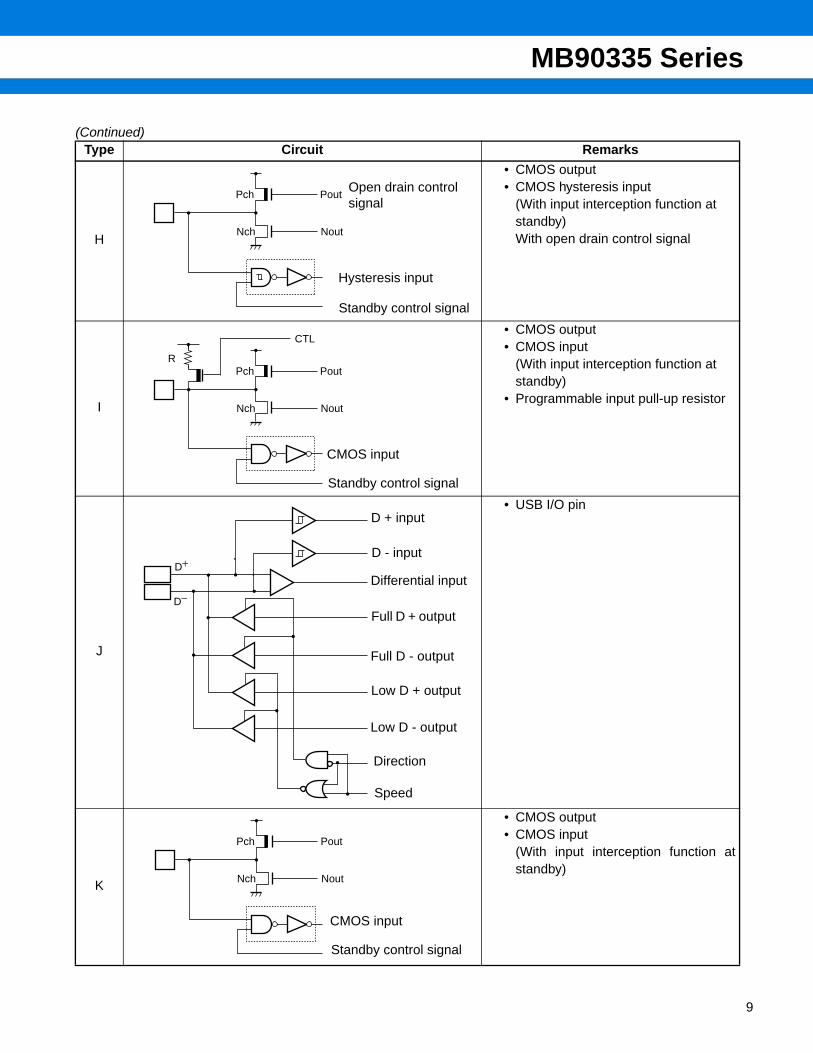
H
• CMOS output• CMOS hysteresis input
(With input interception function at standby) With open drain control signal
I
• CMOS output• CMOS input
(With input interception function at standby)
• Programmable input pull-up resistor
J
• USB I/O pin
K
• CMOS output• CMOS input
(With input interception function atstandby)
Pout
Nout
Pch
Nch
Open drain control signal
Standby control signal
Hysteresis input
Pout
Nout
Pch
Nch
CTL
R
CMOS input
Standby control signal
D+
D−
D + input
D - input
Differential input
Full D + output
Full D - output
Low D + output
Low D - output
Direction
Speed
Pout
Nout
Pch
Nch
CMOS input
Standby control signal
9
MB90335 Series
10
HANDLING DEVICES1. Preventing latchup and turning on power supply
Latchup may occur on CMOS IC under the following conditions:
• If a voltage higher than VCC or lower than VSS is applied to input and output pins.
• A voltage higher than the rated voltage is applied between VCC and VSS.
When latchup occurs, power supply current increases rapidly and might thermally damage elements. Whenusing CMOS IC, take great care to prevent the occurrence of latchup.
2. Treatment of unused pins
Leaving unused input pins unconnected can cause abnormal operation or latchup, leading to permanent damage.Unused input pins should always be pulled up or down through resistance of at least 2 kΩ. Any unused input/output pins may be set to output mode and left open, or set to input mode and treated the same as unused inputpins. If there is unused output pin, make it to open.
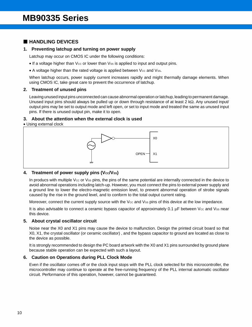
3. About the attention when the external clock is used• Using external clock
4. Treatment of power supply pins (VCC/VSS)
In producs with multiple VCC or VSS pins, the pins of the same potential are internally connected in the device toavoid abnormal operations including latch-up. However, you must connect the pins to external power supply anda ground line to lower the electro-magnetic emission level, to prevent abnormal operation of strobe signalscaused by the rise in the ground level, and to conform to the total output current rating.
Moreover, connect the current supply source with the VCC and VSS pins of this device at the low impedance.
It is also advisable to connect a ceramic bypass capacitor of approximately 0.1 µF between VCC and VSS nearthis device.
5. About crystal oscillator circuit
Noise near the X0 and X1 pins may cause the device to malfunction. Design the printed circuit board so thatX0, X1, the crystal oscillator (or ceramic oscillator) , and the bypass capacitor to ground are located as close tothe device as possible.
It is strongly recommended to design the PC board artwork with the X0 and X1 pins surrounded by ground planebecause stable operation can be expected with such a layout.
6. Caution on Operations during PLL Clock Mode
Even if the oscillator comes off or the clock input stops with the PLL clock selected for this microcontroller, themicrocontroller may continue to operate at the free-running frequency of the PLL internal automatic oscillatorcircuit. Performance of this operation, however, cannot be guaranteed.
X0
X1OPEN
MB90335 Series
7. Stabilization of supply voltage
A sudden change in the supply voltage may cause the device to malfunction even within the VCC supply voltageoperating range. For stabilization reference, the supply voltage should be stabilized so that VCC ripple variations(peak-to-peak value) at commercial frequencies (50 MHz to 60 MHz) fall below 10% of the standard VCC supplyvoltage and the transient regulation does not exceed 0.1 V/ms at temporary changes such as power supplyswitching.
8. Writing to flash memory
For serial writing to flash memory, always make sure that the operating voltage VCC is between 3.13 V and 3.6 V.
For normal writing to flash memory, always make sure that the operating voltage VCC is between 3.0 V and 3.6 V.
11
MB90335 Series
12
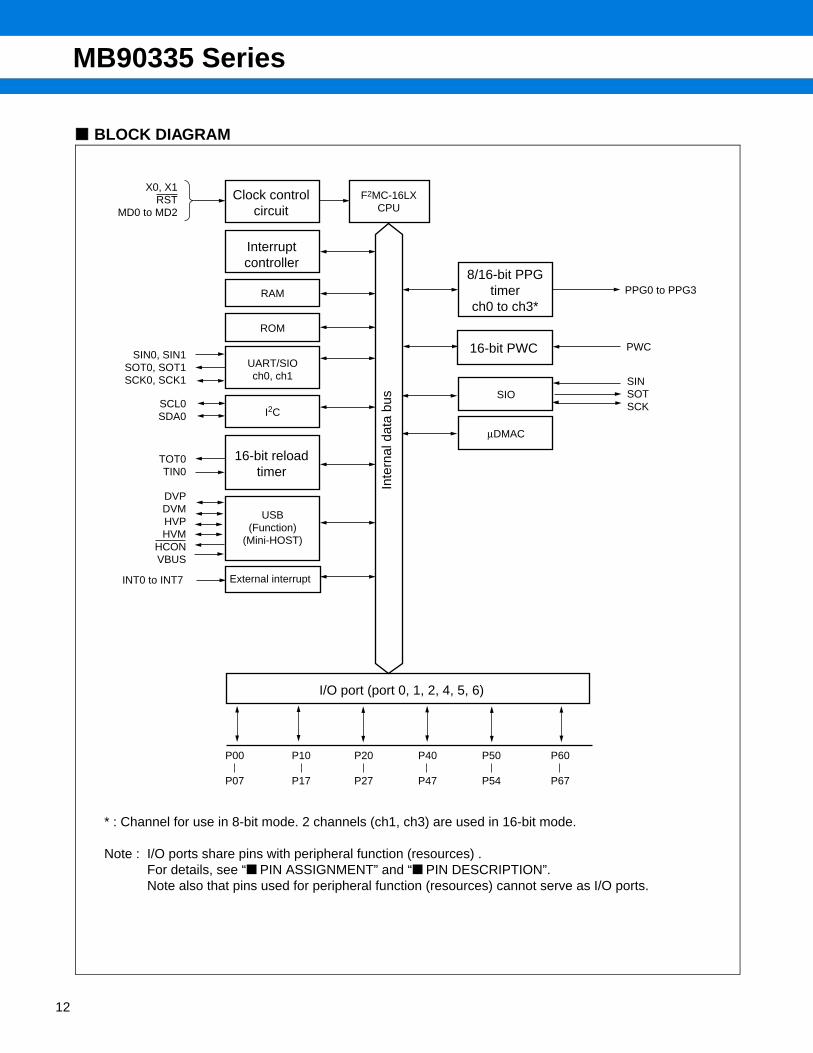
BLOCK DIAGRAM
F2MC-16LXCPU
RAM
ROM
UART/SIOch0, ch1
I2C
SIO
µDMAC
USB(Function)
(Mini-HOST)
P00
P07
P10
P17
P20
P27
P40
P47
P50
P54
P60
P67
X0, X1RST
MD0 to MD2
SIN0, SIN1SOT0, SOT1SCK0, SCK1
SCL0SDA0
INT0 to INT7
DVPDVMHVPHVM
HCONVBUS
TOT0TIN0
PPG0 to PPG3
PWC
SINSOTSCK
* : Channel for use in 8-bit mode. 2 channels (ch1, ch3) are used in 16-bit mode.
Note : I/O ports share pins with peripheral function (resources) .For details, see “ PIN ASSIGNMENT” and “ PIN DESCRIPTION”.Note also that pins used for peripheral function (resources) cannot serve as I/O ports.
16-bit reload timer
External interrupt
16-bit PWC
8/16-bit PPG timer
ch0 to ch3*
Clock control circuit
Interrupt controller
Inte
rnal
dat
a bu
s
I/O port (port 0, 1, 2, 4, 5, 6)
MB90335 Series
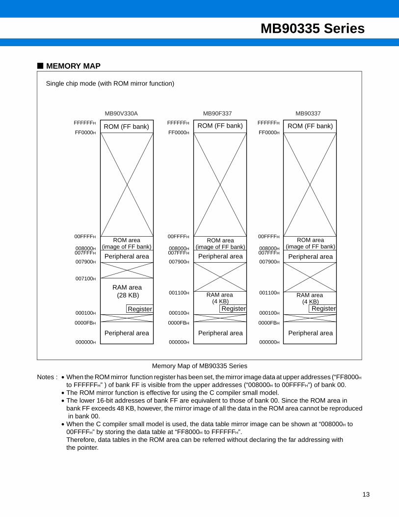
MEMORY MAP
Memory Map of MB90335 Series
Notes : • When the ROM mirror function register has been set, the mirror image data at upper addresses (“FF8000H to FFFFFFH” ) of bank FF is visible from the upper addresses (“008000H to 00FFFFH”) of bank 00.
• The ROM mirror function is effective for using the C compiler small model.• The lower 16-bit addresses of bank FF are equivalent to those of bank 00. Since the ROM area in
bank FF exceeds 48 KB, however, the mirror image of all the data in the ROM area cannot be reproduced in bank 00.
• When the C compiler small model is used, the data table mirror image can be shown at “008000H to 00FFFFH” by storing the data table at “FF8000H to FFFFFFH”. Therefore, data tables in the ROM area can be referred without declaring the far addressing with the pointer.
FFFFFFH
00FFFFH
007FFFH
007900H
007100H
008000H
FF0000H
000100H
0000FBH
000000H
FFFFFFH
00FFFFH
007FFFH
007900H
001100H
008000H
FF0000H
000100H
0000FBH
000000H
FFFFFFH
00FFFFH
007FFFH
007900H
001100H
008000H
FF0000H
000100H
0000FBH
000000H
MB90V330A MB90F337 MB90337
Single chip mode (with ROM mirror function)
Peripheral area
ROM (FF bank)
ROM area(image of FF bank)
Register
RAM area (28 KB)
Peripheral area
Peripheral area
ROM (FF bank)
ROM area(image of FF bank)
Register
RAM area (4 KB)
Peripheral area
Peripheral area
ROM (FF bank)
ROM area(image of FF bank)
Register
RAM area (4 KB)
Peripheral area
13
MB90335 Series
14
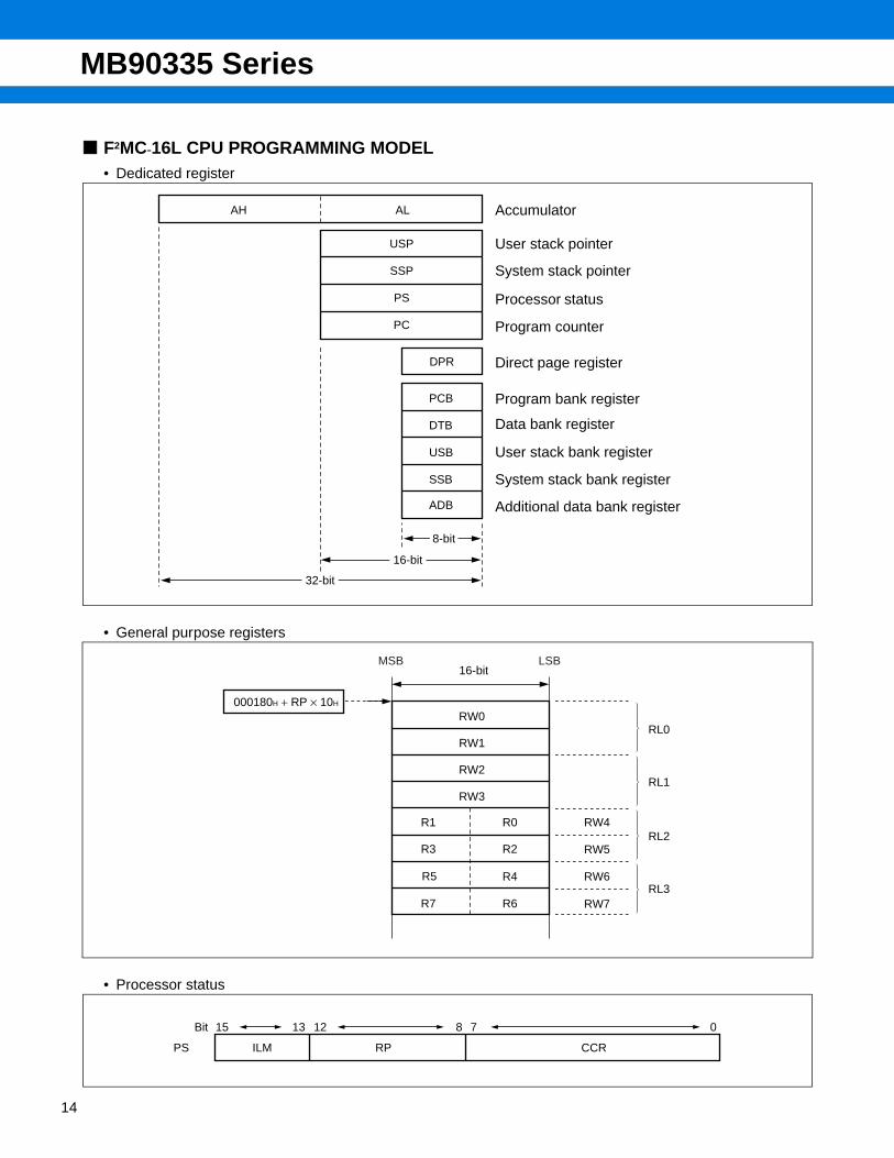
F2MC-16L CPU PROGRAMMING MODEL• Dedicated register
• General purpose registers
• Processor status
AH AL
DPR
PCB
DTB
USB
SSB
ADB
8-bit
16-bit
32-bit
USP
SSP
PS
PC
Accumulator
User stack pointer
System stack pointer
Processor status
Program counter
Direct page register
Program bank register
Data bank register
User stack bank register
System stack bank register
Additional data bank register
R1 R0
R3 R2
R5 R4
R7 R6
RW0
RW1
RW2
RW3
16-bit
000180H + RP × 10H
RW4
RW5
RW6
RW7
RL0
RL1
RL2
RL3
MSB LSB
ILM
15 13
PS RP CCR
12 8 7 0Bit
MB90335 Series
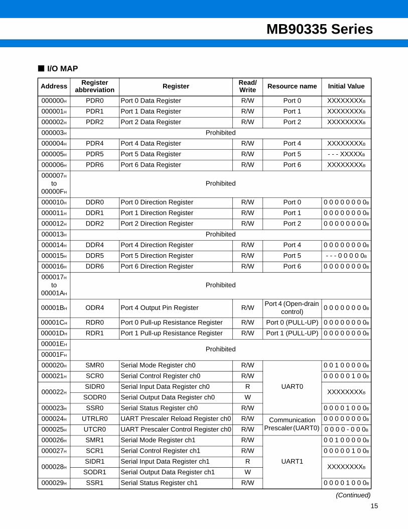
I/O MAP
(Continued)
Address Register abbreviation Register Read/
Write Resource name Initial Value
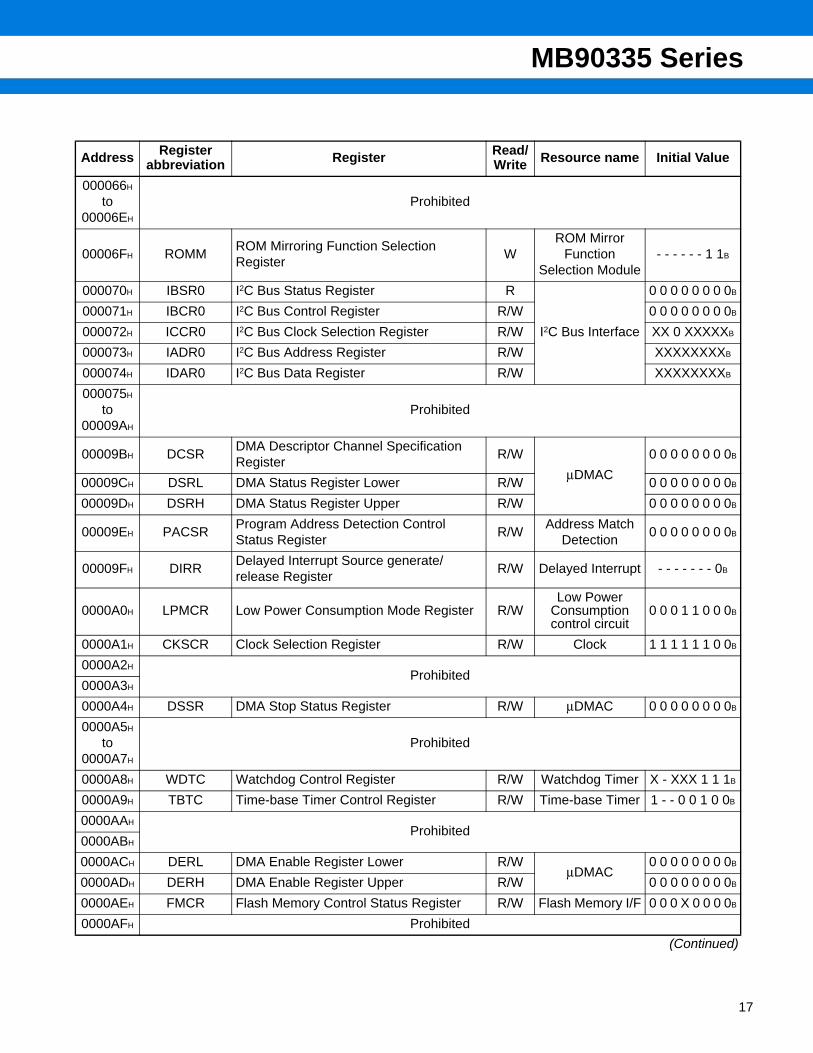
000000H PDR0 Port 0 Data Register R/W Port 0 XXXXXXXXB
000001H PDR1 Port 1 Data Register R/W Port 1 XXXXXXXXB
000002H PDR2 Port 2 Data Register R/W Port 2 XXXXXXXXB
000003H Prohibited
000004H PDR4 Port 4 Data Register R/W Port 4 XXXXXXXXB
000005H PDR5 Port 5 Data Register R/W Port 5 - - - XXXXXB
000006H PDR6 Port 6 Data Register R/W Port 6 XXXXXXXXB
000007H
to00000FH
Prohibited
000010H DDR0 Port 0 Direction Register R/W Port 0 0 0 0 0 0 0 0 0B
000011H DDR1 Port 1 Direction Register R/W Port 1 0 0 0 0 0 0 0 0B
000012H DDR2 Port 2 Direction Register R/W Port 2 0 0 0 0 0 0 0 0B
000013H Prohibited
000014H DDR4 Port 4 Direction Register R/W Port 4 0 0 0 0 0 0 0 0B
000015H DDR5 Port 5 Direction Register R/W Port 5 - - - 0 0 0 0 0B
000016H DDR6 Port 6 Direction Register R/W Port 6 0 0 0 0 0 0 0 0B
000017H
to00001AH
Prohibited
00001BH ODR4 Port 4 Output Pin Register R/WPort 4 (Open-drain
control) 0 0 0 0 0 0 0 0B
00001CH RDR0 Port 0 Pull-up Resistance Register R/W Port 0 (PULL-UP) 0 0 0 0 0 0 0 0B
00001DH RDR1 Port 1 Pull-up Resistance Register R/W Port 1 (PULL-UP) 0 0 0 0 0 0 0 0B
00001EHProhibited
00001FH
000020H SMR0 Serial Mode Register ch0 R/W
UART0
0 0 1 0 0 0 0 0B
000021H SCR0 Serial Control Register ch0 R/W 0 0 0 0 0 1 0 0B
000022HSIDR0 Serial Input Data Register ch0 R
XXXXXXXXBSODR0 Serial Output Data Register ch0 W
000023H SSR0 Serial Status Register ch0 R/W 0 0 0 0 1 0 0 0B
000024H UTRLR0 UART Prescaler Reload Register ch0 R/W Communication Prescaler (UART0)
0 0 0 0 0 0 0 0B
000025H UTCR0 UART Prescaler Control Register ch0 R/W 0 0 0 0 - 0 0 0B
000026H SMR1 Serial Mode Register ch1 R/W
UART1
0 0 1 0 0 0 0 0B
000027H SCR1 Serial Control Register ch1 R/W 0 0 0 0 0 1 0 0B
000028HSIDR1 Serial Input Data Register ch1 R
XXXXXXXXBSODR1 Serial Output Data Register ch1 W
000029H SSR1 Serial Status Register ch1 R/W 0 0 0 0 1 0 0 0B
15
MB90335 Series
16
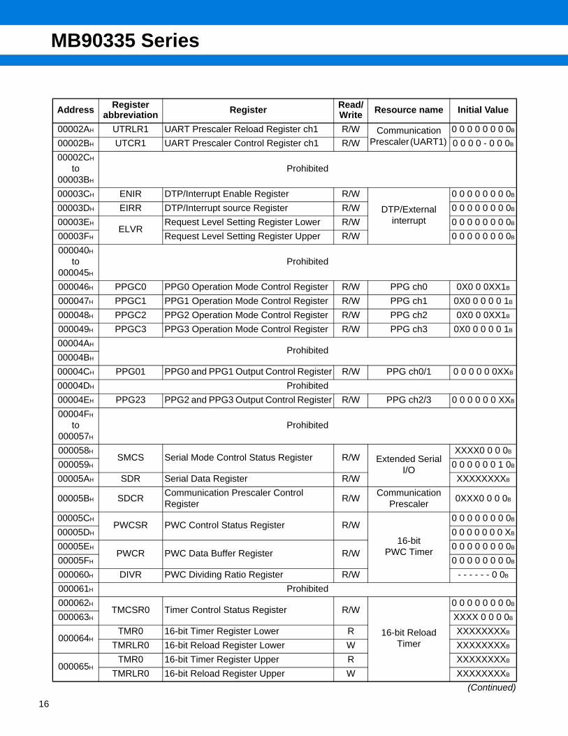
(Continued)
Address Register abbreviation Register Read/
Write Resource name Initial Value
00002AH UTRLR1 UART Prescaler Reload Register ch1 R/W Communication Prescaler (UART1)
0 0 0 0 0 0 0 0B
00002BH UTCR1 UART Prescaler Control Register ch1 R/W 0 0 0 0 - 0 0 0B
00002CH
to00003BH
Prohibited
00003CH ENIR DTP/Interrupt Enable Register R/W
DTP/External interrupt
0 0 0 0 0 0 0 0B
00003DH EIRR DTP/Interrupt source Register R/W 0 0 0 0 0 0 0 0B
00003EHELVR
Request Level Setting Register Lower R/W 0 0 0 0 0 0 0 0B
00003FH Request Level Setting Register Upper R/W 0 0 0 0 0 0 0 0B
000040H
to000045H
Prohibited
000046H PPGC0 PPG0 Operation Mode Control Register R/W PPG ch0 0X0 0 0XX1B
000047H PPGC1 PPG1 Operation Mode Control Register R/W PPG ch1 0X0 0 0 0 0 1B
000048H PPGC2 PPG2 Operation Mode Control Register R/W PPG ch2 0X0 0 0XX1B
000049H PPGC3 PPG3 Operation Mode Control Register R/W PPG ch3 0X0 0 0 0 0 1B
00004AHProhibited
00004BH
00004CH PPG01 PPG0 and PPG1 Output Control Register R/W PPG ch0/1 0 0 0 0 0 0XXB
00004DH Prohibited
00004EH PPG23 PPG2 and PPG3 Output Control Register R/W PPG ch2/3 0 0 0 0 0 0 XXB
00004FH
to000057H
Prohibited
000058HSMCS Serial Mode Control Status Register R/W Extended Serial
I/O
XXXX0 0 0 0B
000059H 0 0 0 0 0 0 1 0B
00005AH SDR Serial Data Register R/W XXXXXXXXB
00005BH SDCRCommunication Prescaler Control Register
R/WCommunication
Prescaler0XXX0 0 0 0B
00005CHPWCSR PWC Control Status Register R/W
16-bitPWC Timer
0 0 0 0 0 0 0 0B
00005DH 0 0 0 0 0 0 0 XB
00005EHPWCR PWC Data Buffer Register R/W
0 0 0 0 0 0 0 0B
00005FH 0 0 0 0 0 0 0 0B
000060H DIVR PWC Dividing Ratio Register R/W - - - - - - 0 0B
000061H Prohibited
000062HTMCSR0 Timer Control Status Register R/W
16-bit Reload Timer
0 0 0 0 0 0 0 0B
000063H XXXX 0 0 0 0B
000064HTMR0 16-bit Timer Register Lower R XXXXXXXXB
TMRLR0 16-bit Reload Register Lower W XXXXXXXXB
000065HTMR0 16-bit Timer Register Upper R XXXXXXXXB
TMRLR0 16-bit Reload Register Upper W XXXXXXXXB
MB90335 Series
(Continued)
Address Register abbreviation Register Read/
Write Resource name Initial Value
000066H
to00006EH
Prohibited
00006FH ROMMROM Mirroring Function Selection Register
WROM Mirror
FunctionSelection Module
- - - - - - 1 1B
000070H IBSR0 I2C Bus Status Register R
I2C Bus Interface
0 0 0 0 0 0 0 0B
000071H IBCR0 I2C Bus Control Register R/W 0 0 0 0 0 0 0 0B
000072H ICCR0 I2C Bus Clock Selection Register R/W XX 0 XXXXXB
000073H IADR0 I2C Bus Address Register R/W XXXXXXXXB
000074H IDAR0 I2C Bus Data Register R/W XXXXXXXXB
000075H
to00009AH
Prohibited
00009BH DCSRDMA Descriptor Channel Specification Register
R/W
µDMAC
0 0 0 0 0 0 0 0B
00009CH DSRL DMA Status Register Lower R/W 0 0 0 0 0 0 0 0B
00009DH DSRH DMA Status Register Upper R/W 0 0 0 0 0 0 0 0B
00009EH PACSRProgram Address Detection Control Status Register
R/WAddress Match
Detection0 0 0 0 0 0 0 0B
00009FH DIRRDelayed Interrupt Source generate/release Register
R/W Delayed Interrupt - - - - - - - 0B
0000A0H LPMCR Low Power Consumption Mode Register R/WLow Power
Consumption control circuit
0 0 0 1 1 0 0 0B
0000A1H CKSCR Clock Selection Register R/W Clock 1 1 1 1 1 1 0 0B
0000A2HProhibited
0000A3H
0000A4H DSSR DMA Stop Status Register R/W µDMAC 0 0 0 0 0 0 0 0B
0000A5H
to0000A7H
Prohibited
0000A8H WDTC Watchdog Control Register R/W Watchdog Timer X - XXX 1 1 1B
0000A9H TBTC Time-base Timer Control Register R/W Time-base Timer 1 - - 0 0 1 0 0B
0000AAHProhibited
0000ABH
0000ACH DERL DMA Enable Register Lower R/WµDMAC
0 0 0 0 0 0 0 0B
0000ADH DERH DMA Enable Register Upper R/W 0 0 0 0 0 0 0 0B
0000AEH FMCR Flash Memory Control Status Register R/W Flash Memory I/F 0 0 0 X 0 0 0 0B
0000AFH Prohibited
17
MB90335 Series
18
(Continued)
Address Register abbreviation Register Read/
Write Resource name Initial Value
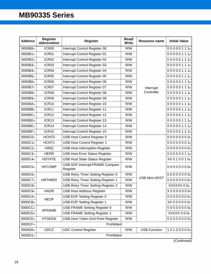
0000B0H ICR00 Interrupt Control Register 00 R/W
Interrupt Controller
0 0 0 0 0 1 1 1B
0000B1H ICR01 Interrupt Control Register 01 R/W 0 0 0 0 0 1 1 1B
0000B2H ICR02 Interrupt Control Register 02 R/W 0 0 0 0 0 1 1 1B
0000B3H ICR03 Interrupt Control Register 03 R/W 0 0 0 0 0 1 1 1B
0000B4H ICR04 Interrupt Control Register 04 R/W 0 0 0 0 0 1 1 1B
0000B5H ICR05 Interrupt Control Register 05 R/W 0 0 0 0 0 1 1 1B
0000B6H ICR06 Interrupt Control Register 06 R/W 0 0 0 0 0 1 1 1B
0000B7H ICR07 Interrupt Control Register 07 R/W 0 0 0 0 0 1 1 1B
0000B8H ICR08 Interrupt Control Register 08 R/W 0 0 0 0 0 1 1 1B
0000B9H ICR09 Interrupt Control Register 09 R/W 0 0 0 0 0 1 1 1B
0000BAH ICR10 Interrupt Control Register 10 R/W 0 0 0 0 0 1 1 1B
0000BBH ICR11 Interrupt Control Register 11 R/W 0 0 0 0 0 1 1 1B
0000BCH ICR12 Interrupt Control Register 12 R/W 0 0 0 0 0 1 1 1B
0000BDH ICR13 Interrupt Control Register 13 R/W 0 0 0 0 0 1 1 1B
0000BEH ICR14 Interrupt Control Register 14 R/W 0 0 0 0 0 1 1 1B
0000BFH ICR15 Interrupt Control Register 15 R/W 0 0 0 0 0 1 1 1B
0000C0H HCNT0 USB Host Control Register 0 R/W
USB Mini-HOST
0 0 0 0 0 0 0 0B
0000C1H HCNT1 USB Host Control Register 1 R/W 0 0 0 0 0 0 0 1B
0000C2H HIRQ USB Host Interruption Register R/W 0 0 0 0 0 0 0 0B
0000C3H HERR USB Host Error Status Register R/W 0 0 0 0 0 0 1 1B
0000C4H HSTATE USB Host State Status Register R/W XX 0 1 0 0 1 0B
0000C5H HFCOMPUSB SOF Interrupt FRAME Compare Register
R/W 0 0 0 0 0 0 0 0B
0000C6H
HRTIMER
USB Retry Timer Setting Register 0 R/W 0 0 0 0 0 0 0 0B
0000C7H USB Retry Timer Setting Register 1 R/W 0 0 0 0 0 0 0 0B
0000C8H USB Retry Timer Setting Register 2 R/W XXXXXX 0 0B
0000C9H HADR USB Host Address Register R/W X 0 0 0 0 0 0 0B
0000CAHHEOF
USB EOF Setting Register 0 R/W 0 0 0 0 0 0 0 0B
0000CBH USB EOF Setting Register 1 R/W XX 0 0 0 0 0 0B
0000CCHHFRAME
USB FRAME Setting Register 0 R/W 0 0 0 0 0 0 0 0B
0000CDH USB FRAME Setting Register 1 R/W XXXXX 0 0 0B
0000CEH HTOKEN USB Host Token End Point Register R/W 0 0 0 0 0 0 0 0B
0000CFH Prohibited
0000D0H UDCC UDC Control Register R/W USB Function 1 0 1 0 0 0 0 0B
0000D1H Prohibited
MB90335 Series
(Continued)
Address Register abbreviation Register Read/
Write Resource name Initial Value
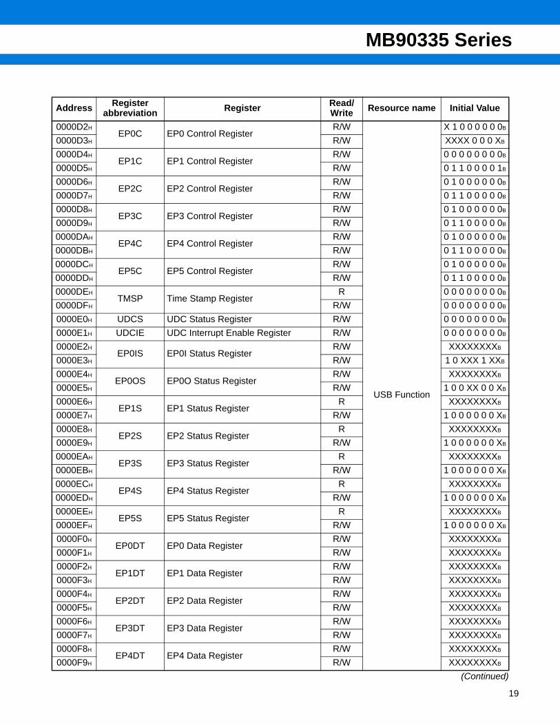
0000D2HEP0C EP0 Control Register
R/W
USB Function
X 1 0 0 0 0 0 0B
0000D3H R/W XXXX 0 0 0 XB
0000D4HEP1C EP1 Control Register
R/W 0 0 0 0 0 0 0 0B
0000D5H R/W 0 1 1 0 0 0 0 1B
0000D6HEP2C EP2 Control Register
R/W 0 1 0 0 0 0 0 0B
0000D7H R/W 0 1 1 0 0 0 0 0B
0000D8HEP3C EP3 Control Register
R/W 0 1 0 0 0 0 0 0B
0000D9H R/W 0 1 1 0 0 0 0 0B
0000DAHEP4C EP4 Control Register
R/W 0 1 0 0 0 0 0 0B
0000DBH R/W 0 1 1 0 0 0 0 0B
0000DCHEP5C EP5 Control Register
R/W 0 1 0 0 0 0 0 0B
0000DDH R/W 0 1 1 0 0 0 0 0B
0000DEHTMSP Time Stamp Register
R 0 0 0 0 0 0 0 0B
0000DFH R/W 0 0 0 0 0 0 0 0B
0000E0H UDCS UDC Status Register R/W 0 0 0 0 0 0 0 0B
0000E1H UDCIE UDC Interrupt Enable Register R/W 0 0 0 0 0 0 0 0B
0000E2HEP0IS EP0I Status Register
R/W XXXXXXXXB
0000E3H R/W 1 0 XXX 1 XXB
0000E4HEP0OS EP0O Status Register
R/W XXXXXXXXB
0000E5H R/W 1 0 0 XX 0 0 XB
0000E6HEP1S EP1 Status Register
R XXXXXXXXB
0000E7H R/W 1 0 0 0 0 0 0 XB
0000E8HEP2S EP2 Status Register
R XXXXXXXXB
0000E9H R/W 1 0 0 0 0 0 0 XB
0000EAHEP3S EP3 Status Register
R XXXXXXXXB
0000EBH R/W 1 0 0 0 0 0 0 XB
0000ECHEP4S EP4 Status Register
R XXXXXXXXB
0000EDH R/W 1 0 0 0 0 0 0 XB
0000EEHEP5S EP5 Status Register
R XXXXXXXXB
0000EFH R/W 1 0 0 0 0 0 0 XB
0000F0HEP0DT EP0 Data Register
R/W XXXXXXXXB
0000F1H R/W XXXXXXXXB
0000F2HEP1DT EP1 Data Register
R/W XXXXXXXXB
0000F3H R/W XXXXXXXXB
0000F4HEP2DT EP2 Data Register
R/W XXXXXXXXB
0000F5H R/W XXXXXXXXB
0000F6HEP3DT EP3 Data Register
R/W XXXXXXXXB
0000F7H R/W XXXXXXXXB
0000F8HEP4DT EP4 Data Register
R/W XXXXXXXXB
0000F9H R/W XXXXXXXXB
19
MB90335 Series
20
(Continued)
Address Register abbreviation Register Read/
Write Resource name Initial Value
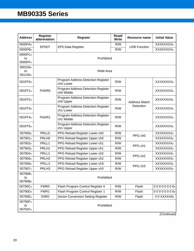
0000FAHEP5DT EP5 Data Register
R/WUSB Function
XXXXXXXXB
0000FBH R/W XXXXXXXXB
0000FCH
to0000FFH
Prohibited
000100H
to001100H
RAM Area
001FF0H
PADR0
Program Address Detection Register ch0 Lower
R/W
Address MatchDetection
XXXXXXXXB
001FF1HProgram Address Detection Register ch0 Middle
R/W XXXXXXXXB
001FF2HProgram Address Detection Register ch0 Upper
R/W XXXXXXXXB
001FF3H
PADR1
Program Address Detection Register ch1 Lower
R/W XXXXXXXXB
001FF4HProgram Address Detection Register ch1 Middle
R/W XXXXXXXXB
001FF5HProgram Address Detection Register ch1 Upper
R/W XXXXXXXXB
007900H PRLL0 PPG Reload Register Lower ch0 R/WPPG ch0
XXXXXXXXB
007901H PRLH0 PPG Reload Register Upper ch0 R/W XXXXXXXXB
007902H PRLL1 PPG Reload Register Lower ch1 R/WPPG ch1
XXXXXXXXB
007903H PRLH1 PPG Reload Register Upper ch1 R/W XXXXXXXXB
007904H PRLL2 PPG Reload Register Lower ch2 R/WPPG ch2
XXXXXXXXB
007905H PRLH2 PPG Reload Register Upper ch2 R/W XXXXXXXXB
007906H PRLL3 PPG Reload Register Lower ch3 R/WPPG ch3
XXXXXXXXB
007907H PRLH3 PPG Reload Register Upper ch3 R/W XXXXXXXXB
007908H
to00790BH
Prohibited
00790CH FWR0 Flash Program Control Register 0 R/W Flash 0 0 0 0 0 0 0 0B
00790DH FWR1 Flash Program Control Register 1 R/W Flash 0 0 0 0 0 0 0 0B
00790EH SSR0 Sector Conversion Setting Register R/W Flash 0 0 XXXXX0B
00790FH
to00791FH
Prohibited
MB90335 Series
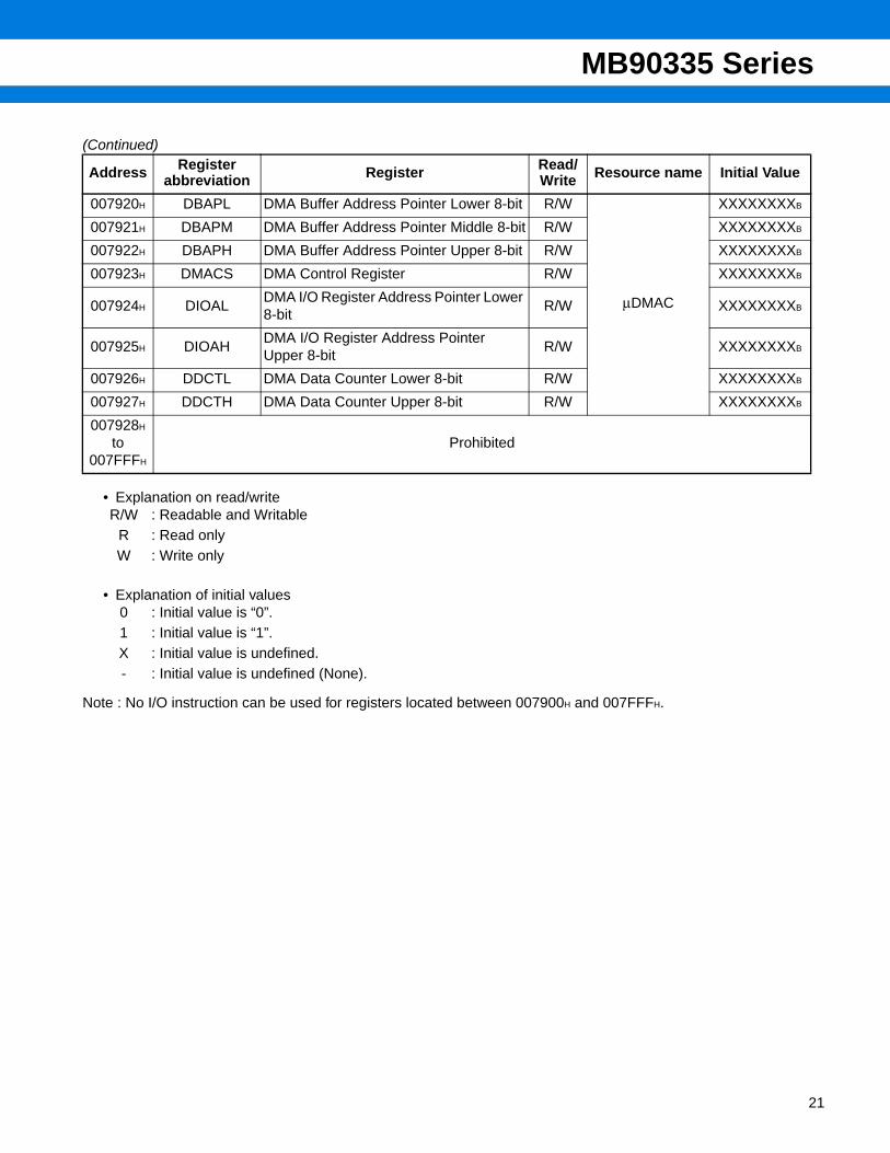
(Continued)
• Explanation on read/write
• Explanation of initial values
Note : No I/O instruction can be used for registers located between 007900H and 007FFFH.
Address Register abbreviation Register Read/
Write Resource name Initial Value
007920H DBAPL DMA Buffer Address Pointer Lower 8-bit R/W
µDMAC
XXXXXXXXB
007921H DBAPM DMA Buffer Address Pointer Middle 8-bit R/W XXXXXXXXB
007922H DBAPH DMA Buffer Address Pointer Upper 8-bit R/W XXXXXXXXB
007923H DMACS DMA Control Register R/W XXXXXXXXB
007924H DIOALDMA I/O Register Address Pointer Lower 8-bit
R/W XXXXXXXXB
007925H DIOAHDMA I/O Register Address Pointer Upper 8-bit
R/W XXXXXXXXB
007926H DDCTL DMA Data Counter Lower 8-bit R/W XXXXXXXXB
007927H DDCTH DMA Data Counter Upper 8-bit R/W XXXXXXXXB
007928H
to007FFFH
Prohibited
R/W : Readable and WritableR : Read onlyW : Write only
0 : Initial value is “0”.1 : Initial value is “1”.X : Initial value is undefined.- : Initial value is undefined (None).
21
MB90335 Series
22
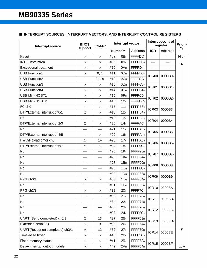
INTERRUPT SOURCES, INTERRUPT VECTORS, AND INTERRUPT CONTROL REGISTERS
Interrupt source EI2OS support µDMAC
Interrupt vector Interrupt control register Priori-
tyNumber* Address ICR Address
Reset × × #08 08H FFFFDCH ⎯ ⎯ High
INT 9 instruction × × #09 09H FFFFD8H ⎯ ⎯
Exceptional treatment × × #10 0AH FFFFD4H ⎯ ⎯
USB Function1 × 0, 1 #11 0BH FFFFD0HICR00 0000B0H
USB Function2 × 2 to 6 #12 0CH FFFFCCH
USB Function3 × × #13 0DH FFFFC8HICR01 0000B1H
USB Function4 × × #14 0EH FFFFC4H
USB Mini-HOST1 × × #15 0FH FFFFC0HICR02 0000B2H
USB Mini-HOST2 × × #16 10H FFFFBCH
I2C ch0 × × #17 11H FFFFB8HICR03 0000B3H
DTP/External interrupt ch0/1 × #18 12H FFFFB4H
No ⎯ ⎯ #19 13H FFFFB0HICR04 0000B4H
DTP/External interrupt ch2/3 × #20 14H FFFFACH
No ⎯ ⎯ #21 15H FFFFA8HICR05 0000B5H
DTP/External interrupt ch4/5 × #22 16H FFFFA4H
PWC/Reload timer ch0 14 #23 17H FFFFA0HICR06 0000B6H
DTP/External interrupt ch6/7 × #24 18H FFFF9CH
No ⎯ ⎯ #25 19H FFFF98HICR07 0000B7H
No ⎯ ⎯ #26 1AH FFFF94H
No ⎯ ⎯ #27 1BH FFFF90HICR08 0000B8H
No ⎯ ⎯ #28 1CH FFFF8CH
No ⎯ ⎯ #29 1DH FFFF88HICR09 0000B9H
PPG ch0/1 × × #30 1EH FFFF84H
No ⎯ ⎯ #31 1FH FFFF80HICR10 0000BAH
PPG ch2/3 × × #32 20H FFFF7CH
No ⎯ ⎯ #33 21H FFFF78HICR11 0000BBH
No ⎯ ⎯ #34 22H FFFF74H
No ⎯ ⎯ #35 23H FFFF70HICR12 0000BCH
No ⎯ ⎯ #36 24H FFFF6CH
UART (Send completed) ch0/1 13 #37 25H FFFF68HICR13 0000BDH
Extended serial I/O × 9 #38 26H FFFF64H
UART(Reception completed) ch0/1 12 #39 27H FFFF60HICR14 0000BEH
Time-base timer × × #40 28H FFFF5CH
Flash memory status × × #41 29H FFFF58HICR15 0000BFH
Delay interrupt output module × × #42 2AH FFFF54H Low
MB90335 Series
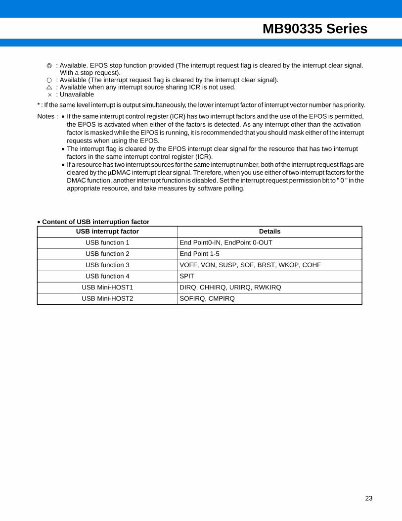
: Available. EI2OS stop function provided (The interrupt request flag is cleared by the interrupt clear signal. With a stop request).
: Available (The interrupt request flag is cleared by the interrupt clear signal). : Available when any interrupt source sharing ICR is not used.
× : Unavailable
* : If the same level interrupt is output simultaneously, the lower interrupt factor of interrupt vector number has priority.
Notes : • If the same interrupt control register (ICR) has two interrupt factors and the use of the EI2OS is permitted, the EI2OS is activated when either of the factors is detected. As any interrupt other than the activation factor is masked while the EI2OS is running, it is recommended that you should mask either of the interrupt requests when using the EI2OS.
• The interrupt flag is cleared by the EI2OS interrupt clear signal for the resource that has two interrupt factors in the same interrupt control register (ICR).
• If a resource has two interrupt sources for the same interrupt number, both of the interrupt request flags are cleared by the µDMAC interrupt clear signal. Therefore, when you use either of two interrupt factors for the DMAC function, another interrupt function is disabled. Set the interrupt request permission bit to " 0 " in the appropriate resource, and take measures by software polling.
• Content of USB interruption factorUSB interrupt factor Details
USB function 1 End Point0-IN, EndPoint 0-OUT
USB function 2 End Point 1-5
USB function 3 VOFF, VON, SUSP, SOF, BRST, WKOP, COHF
USB function 4 SPIT
USB Mini-HOST1 DIRQ, CHHIRQ, URIRQ, RWKIRQ
USB Mini-HOST2 SOFIRQ, CMPIRQ
23
MB90335 Series
24
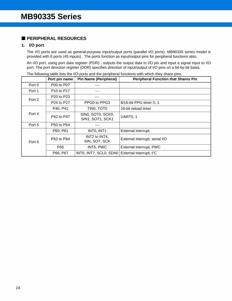
PERIPHERAL RESOURCES1. I/O port
The I/O ports are used as general-purpose input/output ports (parallel I/O ports). MB90335 series model isprovided with 6 ports (45 inputs) . The ports function as input/output pins for peripheral functions also.
An I/O port, using port data register (PDR) , outputs the output data to I/O pin and input a signal input to I/Oport. The port direction register (DDR) specifies direction of input/output of I/O pins on a bit-by-bit basis.
The following table lists the I/O ports and the peripheral functions with which they share pins.Port pin name Pin Name (Peripheral) Peripheral Function that Shares Pin
Port 0 P00 to P07 ⎯
Port 1 P10 to P17 ⎯
Port 2P20 to P23 ⎯
P24 to P27 PPG0 to PPG3 8/16-bit PPG timer 0, 1
Port 4P40, P41 TIN0, TOT0 16-bit reload timer
P42 to P47SIN0, SOT0, SCK0, SIN1, SOT1, SCK1
UART0, 1
Port 5 P50 to P54 ⎯
Port 6
P60, P61 INT0, INT1 External interrupt
P62 to P64INT2 to INT4,
SIN, SOT, SCKExternal interrupt, serial I/O
P65 INT5, PWC External interrupt, PWC
P66, P67 INT6, INT7, SCL0, SDA0 External interrupt, I2C
MB90335 Series
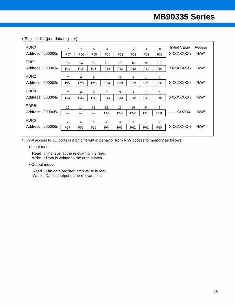
• Register list (port data register)
* : R/W access to I/O ports is a bit different in behavior from R/W access to memory as follows:
• Input mode
Read : The level at the relevant pin is read.Write : Data is written to the output latch.
• Output mode
Read : The data register latch value is read.Write : Data is output to the relevant pin.
PDR0 Initial Value Access
Address : 000000H XXXXXXXXB R/W*
PDR1
Address : 000001H XXXXXXXXB R/W*
PDR2
Address : 000002H XXXXXXXXB R/W*
PDR4
Address : 000004H XXXXXXXXB R/W*
PDR5
Address : 000005H - - - XXXXXB R/W*
PDR6
Address : 000006H XXXXXXXXB R/W*
7 6 5 4 3 2 1 0
P06P07 P05 P04 P03 P02 P01 P00
15 14 13 12 11 10 9 8
P16P17 P15 P14 P13 P12 P11 P10
7 6 5 4 3 2 1 0
P26P27 P25 P24 P23 P22 P21 P20
7 6 5 4 3 2 1 0
P46P47 P45 P44 P43 P42 P41 P40
15 14 13 12 11 10 9 8
⎯⎯ ⎯ P54 P53 P52 P51 P50
7 6 5 4 3 2 1 0
P66 P65 P64 P63 P62 P61 P60P67
25
MB90335 Series
26
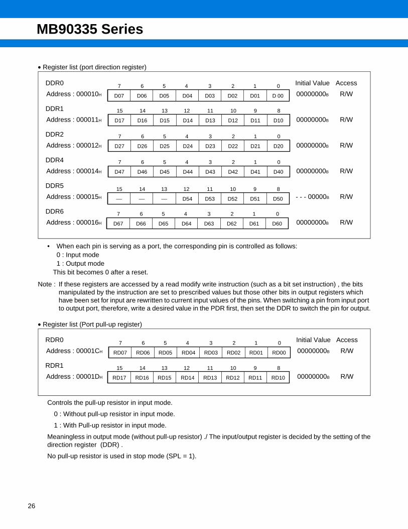
• Register list (port direction register)
• When each pin is serving as a port, the corresponding pin is controlled as follows:0 : Input mode1 : Output mode
This bit becomes 0 after a reset.
Note : If these registers are accessed by a read modify write instruction (such as a bit set instruction) , the bits manipulated by the instruction are set to prescribed values but those other bits in output registers which have been set for input are rewritten to current input values of the pins. When switching a pin from input port to output port, therefore, write a desired value in the PDR first, then set the DDR to switch the pin for output.
• Register list (Port pull-up register)
Controls the pull-up resistor in input mode.
0 : Without pull-up resistor in input mode.
1 : With Pull-up resistor in input mode.
Meaningless in output mode (without pull-up resistor) ./ The input/output register is decided by the setting of thedirection register (DDR) .
No pull-up resistor is used in stop mode (SPL = 1).
DDR0 Initial Value Access
Address : 000010H 00000000B R/W
DDR1
Address : 000011H 00000000B R/W
DDR2
Address : 000012H 00000000B R/W
DDR4
Address : 000014H 00000000B R/W
DDR5
Address : 000015H - - - 00000B R/W
DDR6
Address : 000016H 00000000B R/W
7 6 5 4 3 2 1 0
D06D07 D05 D04 D03 D02 D01 D 00
15 14 13 12 11 10 9 8
D16D17 D15 D14 D13 D12 D11 D10
7 6 5 4 3 2 1 0
D26D27 D25 D24 D23 D22 D21 D20
7 6 5 4 3 2 1 0
D46D47 D45 D44 D43 D42 D41 D40
15 14 13 12 11 10 9 8
⎯⎯ ⎯ D54 D53 D52 D51 D50
7 6 5 4 3 2 1 0
D66D67 D65 D64 D63 D62 D61 D60
RDR0 Initial Value Access
Address : 00001CH 00000000B R/W
RDR1
Address : 00001DH 00000000B R/W
7 6 5 4 3 2 1 0
RD06RD07 RD05 RD04 RD03 RD02 RD01 RD00
15 14 13 12 11 10 9 8
RD16RD17 RD15 RD14 RD13 RD12 RD11 RD10
MB90335 Series
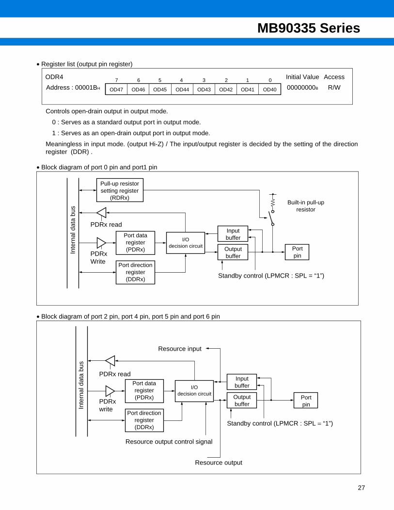
• Register list (output pin register)
Controls open-drain output in output mode.
0 : Serves as a standard output port in output mode.
1 : Serves as an open-drain output port in output mode.
Meaningless in input mode. (output Hi-Z) / The input/output register is decided by the setting of the directionregister (DDR) .
• Block diagram of port 0 pin and port1 pin
• Block diagram of port 2 pin, port 4 pin, port 5 pin and port 6 pin
ODR4 Initial Value Access
Address : 00001BH 00000000B R/W7 6 5 4 3 2 1 0
OD46OD47 OD45 OD44 OD43 OD42 OD41 OD40
Pull-up resistor setting register
(RDRx)
Port data register (PDRx)
Port direction register (DDRx)
I/Odecision circuit
Input buffer
Output buffer
Inte
rnal
dat
a bu
s
PDRx read
PDRxWrite
Port pin
Built-in pull-up resistor
Standby control (LPMCR : SPL = “1”)
Port data register (PDRx)
Port direction register (DDRx)
I/Odecision circuit
Input buffer
Output bufferIn
tern
al d
ata
bus
PDRx read
PDRx write
Port pin
Standby control (LPMCR : SPL = “1”)
Resource output control signal
Resource output
Resource input
27
MB90335 Series
28
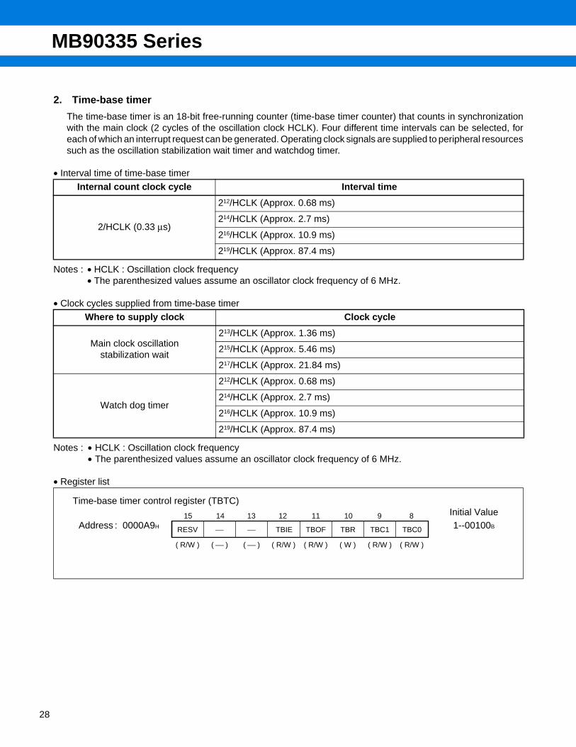
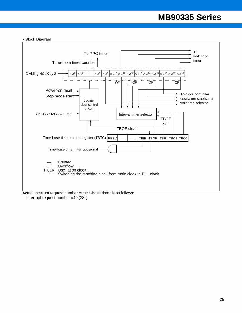
2. Time-base timer
The time-base timer is an 18-bit free-running counter (time-base timer counter) that counts in synchronizationwith the main clock (2 cycles of the oscillation clock HCLK). Four different time intervals can be selected, foreach of which an interrupt request can be generated. Operating clock signals are supplied to peripheral resourcessuch as the oscillation stabilization wait timer and watchdog timer.
• Interval time of time-base timer
Notes : • HCLK : Oscillation clock frequency• The parenthesized values assume an oscillator clock frequency of 6 MHz.
• Clock cycles supplied from time-base timer
Notes : • HCLK : Oscillation clock frequency• The parenthesized values assume an oscillator clock frequency of 6 MHz.
• Register list
Internal count clock cycle Interval time
2/HCLK (0.33 µs)
212/HCLK (Approx. 0.68 ms)
214/HCLK (Approx. 2.7 ms)
216/HCLK (Approx. 10.9 ms)
219/HCLK (Approx. 87.4 ms)
Where to supply clock Clock cycle
Main clock oscillation stabilization wait
213/HCLK (Approx. 1.36 ms)
215/HCLK (Approx. 5.46 ms)
217/HCLK (Approx. 21.84 ms)
Watch dog timer
212/HCLK (Approx. 0.68 ms)
214/HCLK (Approx. 2.7 ms)
216/HCLK (Approx. 10.9 ms)
219/HCLK (Approx. 87.4 ms)
Time-base timer control register (TBTC) Initial Value
Address : 0000A9H 1--00100B
( ⎯ ) ( ⎯ ) ( R/W ) ( R/W ) ( W ) ( R/W ) ( R/W )
15 14 13 12 11 10 9 8
⎯
( R/W )
RESV ⎯ TBIE TBOF TBR TBC1 TBC0
MB90335 Series
• Block Diagram
Actual interrupt request number of time-base timer is as follows:Interrupt request number:#40 (28H)
TBIE TBOF TBRRESV ⎯ ⎯ TBC1 TBC0
OF OF OF OF
× 21 × 22 × 28 × 29 × 210 × 211 × 212 × 213 × 214 × 215 × 216 × 217 × 218
To PPG timer
Time-base timer counter
Dividing HCLK by 2
To watchdog timer
CKSCR : MCS = 1→0*
Counter clear control
circuit
Interval timer selector
TBOF clear
Time-base timer control register (TBTC)
Time-base timer interrupt signal
To clock controller oscillation stabilizing wait time selector
TBOF set
⎯ :UnusedOF :Overflow
HCLK :Oscillation clock* :Switching the machine clock from main clock to PLL clock
Power-on reset
Stop mode start
29
MB90335 Series
30
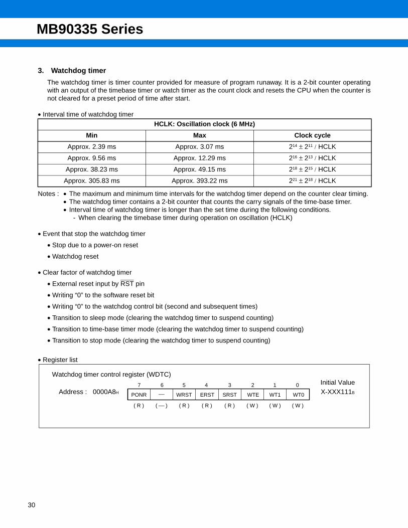
3. Watchdog timer
The watchdog timer is timer counter provided for measure of program runaway. It is a 2-bit counter operatingwith an output of the timebase timer or watch timer as the count clock and resets the CPU when the counter isnot cleared for a preset period of time after start.
• Interval time of watchdog timer
Notes : • The maximum and minimum time intervals for the watchdog timer depend on the counter clear timing.• The watchdog timer contains a 2-bit counter that counts the carry signals of the time-base timer. • Interval time of watchdog timer is longer than the set time during the following conditions.
- When clearing the timebase timer during operation on oscillation (HCLK)
• Event that stop the watchdog timer
• Stop due to a power-on reset
• Watchdog reset
• Clear factor of watchdog timer
• External reset input by RST pin
• Writing “0” to the software reset bit
• Writing “0” to the watchdog control bit (second and subsequent times)
• Transition to sleep mode (clearing the watchdog timer to suspend counting)
• Transition to time-base timer mode (clearing the watchdog timer to suspend counting)
• Transition to stop mode (clearing the watchdog timer to suspend counting)
• Register list
HCLK: Oscillation clock (6 MHz)
Min Max Clock cycle
Approx. 2.39 ms Approx. 3.07 ms 214 ± 211 / HCLK
Approx. 9.56 ms Approx. 12.29 ms 216 ± 213 / HCLK
Approx. 38.23 ms Approx. 49.15 ms 218 ± 215 / HCLK
Approx. 305.83 ms Approx. 393.22 ms 221 ± 218 / HCLK
Watchdog timer control register (WDTC)Initial Value
Address : 0000A8H X-XXX111B
( ⎯ ) ( R ) ( R ) ( R ) ( W ) ( W ) ( W )
7 6 5 4 3 2 1 0
( R )
PONR WRST ERST SRST WTE WT1 WT0⎯
MB90335 Series
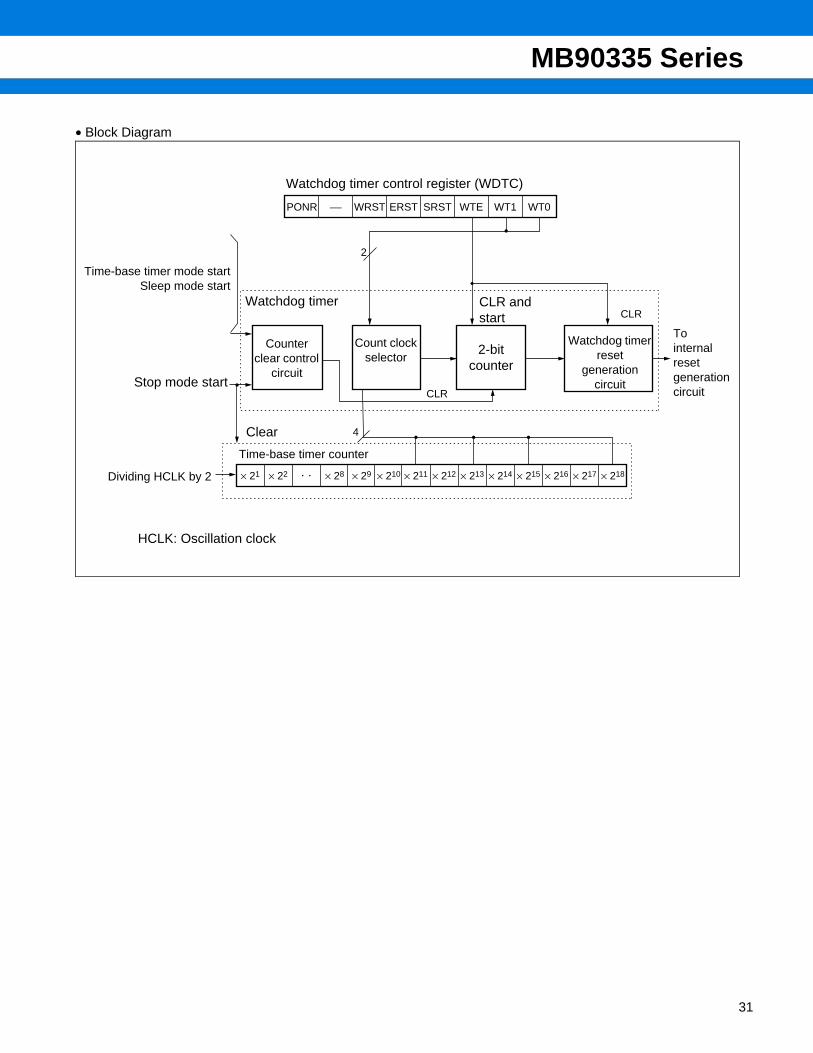
• Block Diagram
PONR ⎯ WRST ERST SRST WTE WT1 WT0
× 21 × 22 × 28 × 29 × 210 × 211 × 212 × 213 × 214 × 215 × 216 × 217 × 218
CLR
CLR
2
4
Watchdog timer control register (WDTC)
Watchdog timer
Time-base timer mode startSleep mode start
Counter clear control
circuit
Count clock selector
2-bit counter
Watchdog timer reset
generation circuit
To internal reset generation circuit
CLR and start
Time-base timer counter
Dividing HCLK by 2
HCLK: Oscillation clock
Clear
Stop mode start
31
MB90335 Series
32
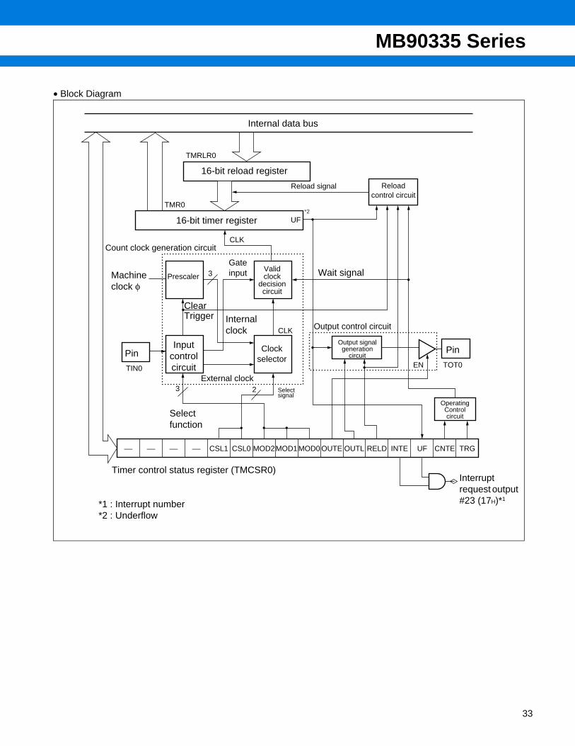
4. 16-bit reload timer
The 16-bit reload timer has the internal clock mode to be decrement in synchronization with 3 different internalclocks and the event count mode to decrement upon detection of an arbitrary edge of the pulse input to theexternal pin. Either can be selected. This timer defines when the count value changes from 0000H to FFFFH asan underflow. The timer therefore causes an underflow when the count reaches [reload register setting +1]. Either mode can be selected for the count operation from the reload mode which repeats the countby reloading the count setting value at the underflow occurrence or the one-shot mode which stops the countat the underflow occurrence. The interrupt can be generated at the counter underflow occurrence so as tocorrespond to the DTC.
• Register list
• Timer control status registerTimer control status register (Upper) (TMCSR0)
Timer control status register (Lower) (TMCSR0)
• 16-bit timer register/16-bit reload registerTMR0/TMRLR0 (Upper)
TMR0/TMRLR0 (Lower)
Initial ValueAddress : 000063H XXXX0000B
Initial ValueAddress : 000062H 00000000B
Initial ValueAddress : 000065H XXXXXXXXB
Initial ValueAddress : 000064H XXXXXXXXB
( ⎯ ) ( ⎯ ) ( ⎯ ) ( R/W ) ( R/W ) ( R/W ) ( R/W )
15 14 13 12 11 10 9 8
⎯
( ⎯ )
⎯ ⎯ ⎯ CSL1 CSL0 MOD2 MOD1
( R/W ) ( R/W ) ( R/W ) ( R/W ) ( R/W ) ( R/W ) ( R/W )
7 6 5 4 3 2 1 0
OUTE
( R/W )
MOD0 OUTL RELD INTE UF CNTE TRG
( R/W ) ( R/W ) ( R/W ) ( R/W ) ( R/W ) ( R/W ) ( R/W )
15 14 13 12 11 10 9 8
D14
( R/W )
D15 D13 D12 D11 D10 D09 D08
( R/W ) ( R/W ) ( R/W ) ( R/W ) ( R/W ) ( R/W ) ( R/W )
7 6 5 4 3 2 1 0
D06
( R/W )
D07 D05 D04 D03 D02 D01 D00
MB90335 Series
• Block Diagram
TMRLR0
TMR0
CLK
TIN0
UF
EN TOT0
CLK
3
3 2
⎯ ⎯ ⎯ ⎯ CSL1 CSL0 MOD2MOD1MOD0 OUTE OUTL RELD UFINTE CNTE TRG
*2
Internal data bus
16-bit reload register
16-bit timer register
Reload signal Reload control circuit
Wait signal
Output control circuit
Output signal generation
circuitPin
Valid clock
decision circuit
Clock selector
Operating Control circuit
Select signal
External clock
Internal clock
Input control circuit
Pin
Prescaler
Count clock generation circuit
Gate input
Timer control status register (TMCSR0) Interrupt request output #23 (17H)*1
Select function
ClearTrigger
Machine clock φ
*1 : Interrupt number*2 : Underflow
33
MB90335 Series
34
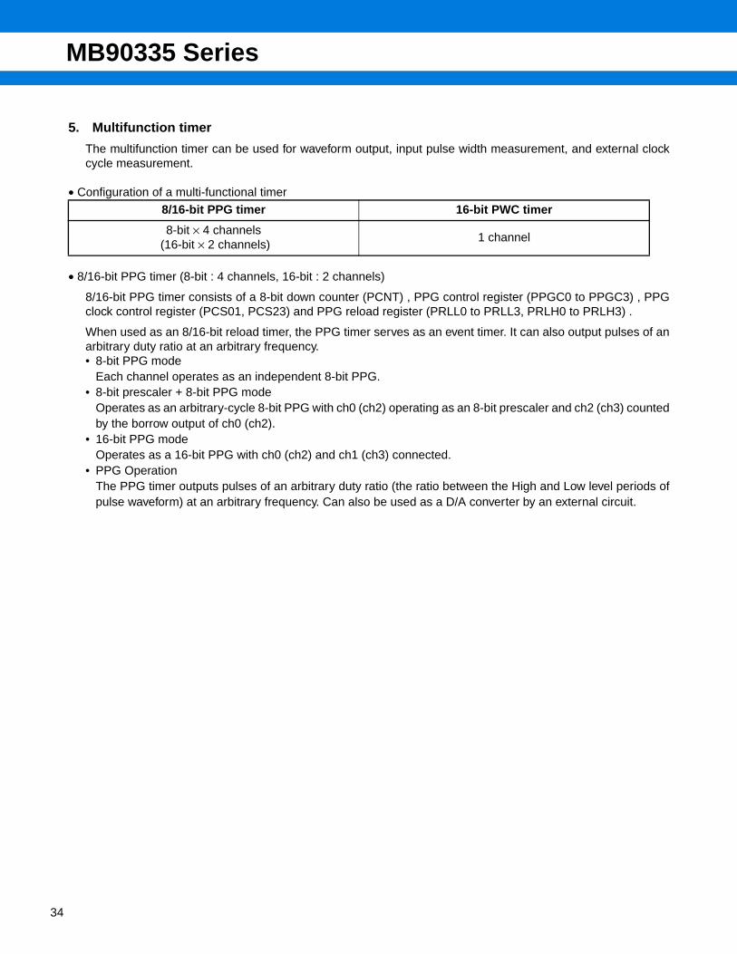
5. Multifunction timer
The multifunction timer can be used for waveform output, input pulse width measurement, and external clockcycle measurement.
• Configuration of a multi-functional timer
• 8/16-bit PPG timer (8-bit : 4 channels, 16-bit : 2 channels)
8/16-bit PPG timer consists of a 8-bit down counter (PCNT) , PPG control register (PPGC0 to PPGC3) , PPGclock control register (PCS01, PCS23) and PPG reload register (PRLL0 to PRLL3, PRLH0 to PRLH3) .
When used as an 8/16-bit reload timer, the PPG timer serves as an event timer. It can also output pulses of anarbitrary duty ratio at an arbitrary frequency.• 8-bit PPG mode
Each channel operates as an independent 8-bit PPG.• 8-bit prescaler + 8-bit PPG mode
Operates as an arbitrary-cycle 8-bit PPG with ch0 (ch2) operating as an 8-bit prescaler and ch2 (ch3) countedby the borrow output of ch0 (ch2).
• 16-bit PPG modeOperates as a 16-bit PPG with ch0 (ch2) and ch1 (ch3) connected.
• PPG OperationThe PPG timer outputs pulses of an arbitrary duty ratio (the ratio between the High and Low level periods ofpulse waveform) at an arbitrary frequency. Can also be used as a D/A converter by an external circuit.
8/16-bit PPG timer 16-bit PWC timer
8-bit × 4 channels (16-bit × 2 channels)
1 channel
MB90335 Series
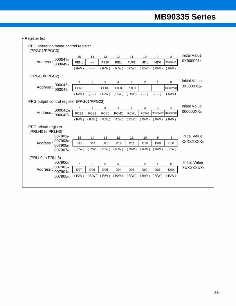
• Register list
PPG operation mode control register (PPGC1/PPGC3)
(PPGC0/PPGC2)
PPG output control register (PPG01/PPG23)
PPG reload register (PRLH0 to PRLH3)
(PRLL0 to PRLL3)
Address :000047H
000049H
Initial Value0X000001B
Address :000046H
000048H
Initial Value0X000XX1B
Address :00004CH
00004EH
Initial Value000000XXB
Address :
007901H
007903H
007905H
007907H
Initial ValueXXXXXXXXB
Address :
007900H
007902H
007904H
007906H
Initial ValueXXXXXXXXB
15 14 13 12 11 10 9 8
( R/W ) ( ⎯ ) ( R/W ) ( R/W ) ( R/W ) ( R/W ) ( R/W ) ( R/W )
⎯PEN1 PE10 PIE1 PUF1 MD1 MD0 Reserved
7 6 5 4 3 2 1 0
( R/W ) ( ⎯ ) ( R/W ) ( R/W ) ( R/W ) ( ⎯ ) ( ⎯ ) ( R/W )
⎯PEN0 PE0O PIE0 PUF0 ⎯ ⎯ Reserved
7 6 5 4 3 2 1 0
( R/W ) ( R/W ) ( R/W ) ( R/W ) ( R/W ) ( R/W ) ( R/W ) ( R/W )
PCS1PCS2 PCS0 PCM2 PCM1 PCM0 ReservedReserved
15 14 13 12 11 10 9 8
( R/W ) ( R/W ) ( R/W ) ( R/W ) ( R/W ) ( R/W ) ( R/W ) ( R/W )
D14D15 D13 D12 D11 D10 D09 D08
7 6 5 4 3 2 1 0
( R/W ) ( R/W ) ( R/W ) ( R/W ) ( R/W ) ( R/W ) ( R/W ) ( R/W )
D06D07 D05 D04 D03 D02 D01 D00
35
MB90335 Series
36
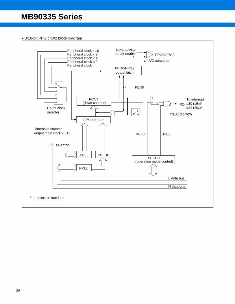
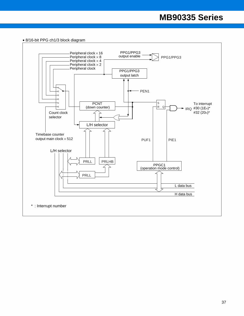
• 8/16-bit PPG ch0/2 block diagram
PPG0/PPG2
PEN0
IRQ
PIE0PUF0
PRLL PRLHB
PRLL
S
R QPCNT
(down counter)
Peripheral clock × 16
PPG0/PPG2output latch
Count clock selector
Timebase counteroutput main clock × 512
ch1/3 borrow
L/H selector
PPGC0 (operation mode control)
* : Interrupt number
To interrupt#30 (1EH)*#32 (20H)*
L/H selector
PPG0/PPG2output enablePeripheral clock × 8
Peripheral clock × 4Peripheral clock × 2Peripheral clock
A/D converter
L data bus
H data bus
MB90335 Series
• 8/16-bit PPG ch1/3 block diagram
PPG1/PPG3
PEN1
IRQ
PIE1PUF1
PRLL PRLHB
PRLL
SR Q
PCNT (down counter)
Peripheral clock × 16
PPG1/PPG3output latch
Count clock selector
Timebase counteroutput main clock × 512
L/H selector
PPGC1 (operation mode control)
* : Interrupt number
To interrupt#30 (1EH)*#32 (20H)*
L/H selector
PPG1/PPG3output enablePeripheral clock × 8
Peripheral clock × 4Peripheral clock × 2Peripheral clock
L data bus
H data bus
37
MB90335 Series
38
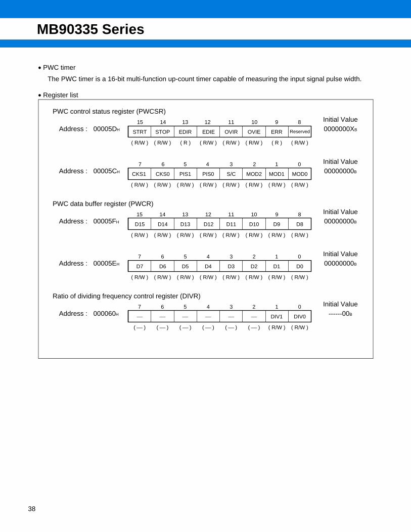
• PWC timer
The PWC timer is a 16-bit multi-function up-count timer capable of measuring the input signal pulse width.
• Register list
PWC control status register (PWCSR)
PWC data buffer register (PWCR)
Ratio of dividing frequency control register (DIVR)
Initial ValueAddress : 00005DH 0000000XB
Initial ValueAddress : 00005CH 00000000B
Initial ValueAddress : 00005FH 00000000B
Initial ValueAddress : 00005EH 00000000B
Initial ValueAddress : 000060H ------00B
( R/W ) ( R ) ( R/W ) ( R/W ) ( R/W ) ( R ) ( R/W )
15 14 13 12 11 10 9 8
STOP
( R/W )
STRT EDIR EDIE OVIR OVIE ERR Reserved
( R/W ) ( R/W ) ( R/W ) ( R/W ) ( R/W ) ( R/W ) ( R/W )
7 6 5 4 3 2 1 0
CKS0
( R/W )
CKS1 PIS1 PIS0 S/C MOD2 MOD1 MOD0
( R/W ) ( R/W ) ( R/W ) ( R/W ) ( R/W ) ( R/W ) ( R/W )
15 14 13 12 11 10 9 8
D14
( R/W )
D15 D13 D12 D11 D10 D9 D8
( R/W ) ( R/W ) ( R/W ) ( R/W ) ( R/W ) ( R/W ) ( R/W )
7 6 5 4 3 2 1 0
D6
( R/W )
D7 D5 D4 D3 D2 D1 D0
( ⎯ ) ( ⎯ ) ( ⎯ ) ( ⎯ ) ( ⎯ ) ( R/W ) ( R/W )
7 6 5 4 3 2 1 0
⎯
( ⎯ )
⎯ ⎯ ⎯ ⎯ ⎯ DIV1 DIV0
MB90335 Series
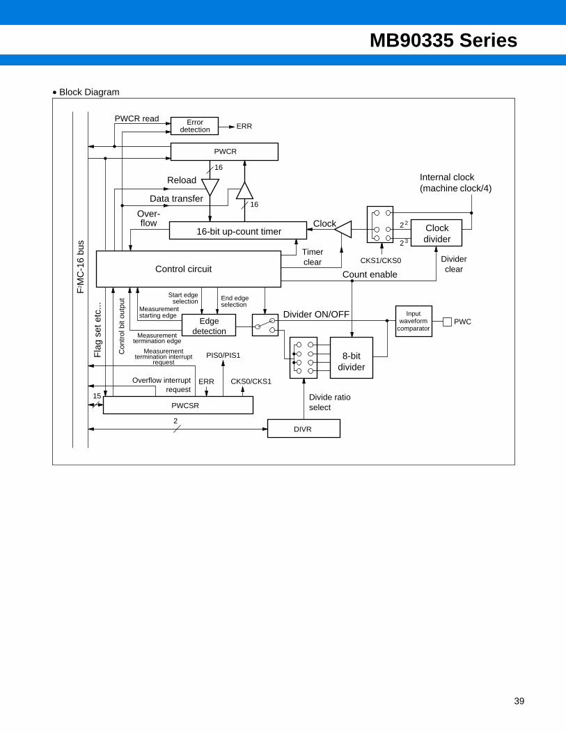
• Block Diagram
ERR
PWCR
16
16
CKS1/CKS0
15
ERR CKS0/CKS1
PIS0/PIS1
PWCSR
DIVR2
2 2
2 3
PWC
PWCR read Error detection
Reload
Data transfer
Over-flow
16-bit up-count timerClock
Internal clock(machine clock/4)
Clock divider
Control circuit
Timer clear
Count enable
Divider clear
Fla
g se
t etc
...
Con
trol
bit
outp
ut
Start edgeselection
Measurement termination edge
End edge selection
Edge detection
Divider ON/OFFMeasurement starting edge
Overflow interruptrequest
Divide ratio select
8-bit divider
F2 M
C-1
6 bu
s
Measurement termination interrupt
request
Input waveform
comparator
39
MB90335 Series
40
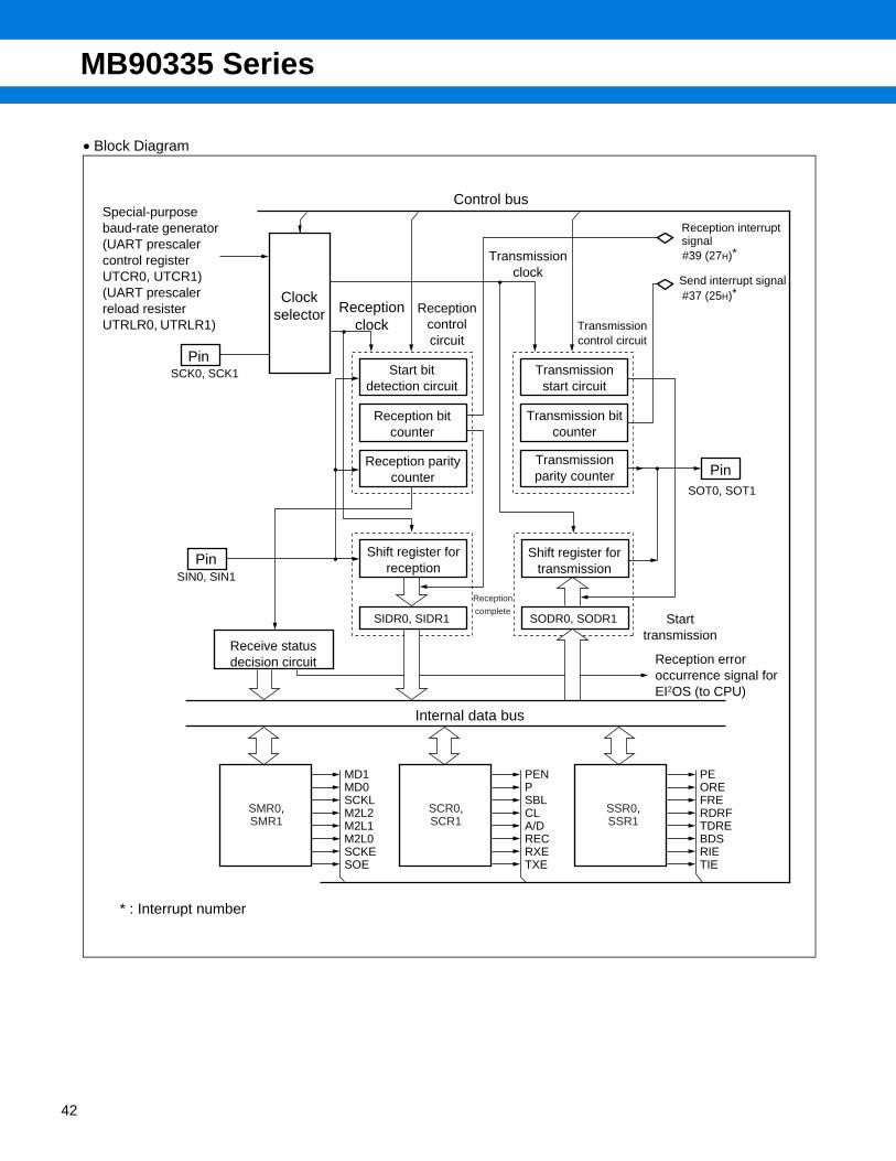
6. UART
UART is a general purpose serial communication interface for synchronous or asynchronous (start-stop syn-chronization) communications with external devices.
It supports bi-directional communication (normal mode) and master/slave communication (multi-processormode: supported on master side only).
An interrupt can be generated upon completion of reception, detection of a reception error, or upon completionof transmission. EI2OS is supported.
• UART functions
UART, or a generic serial data communication interface that sends and receives serial data to and from otherCPU and peripherals, has the functions listed in following.
Note : In clock synchronous transfer mode, the UART transfers only data with no start or stop bit added.
• UART operation modes
⎯ : Setting disabled
*1 : + 1 is an address/data setting bit (A/D) which is used for communication control.
*2 : Only one bit can be detected as a stop bit at reception.
Operation modeData length
Synchronization Stop bit lengthWithout parity With parity
0 Normal mode 7-bit or 8-bit Asynchronous1-bit or 2-bit *2
1 Multi processor mode 8-bit + 1 *1 ⎯ Asynchronous
2 Normal mode 1 to 8-bit ⎯ Synchronous No
Function
Data buffer Full-duplex double-buffered
Transmission mode• Clock synchronous (without start/stop bit) • Clock asynchronous (start-stop synchronous)
Baud rate• Special-purpose baud-rate generator
It is optional from 8 kinds.• Baud rate by external clock (clock of SCK0/SCK1 terminal input)
Data length• 8-bit or 7-bit (in the asynchronous normal mode only)• 1 to 8 bits (in the synchronous mode only)
Signaling system Non Return to Zero (NRZ) system
Reception error detection• Framing error• Overrun error• Parity error (Not supported in operation mode 1)
Interrupt request• Receive interrupt (reception completed, reception error detected)• Transmission interrupt (transmission completed)• Both the transmission and reception support EI2OS.
Master/slave type communication function(multi processor mode)
Capable of 1 (master) to n (slaves) communication (available just as master)
MB90335 Series
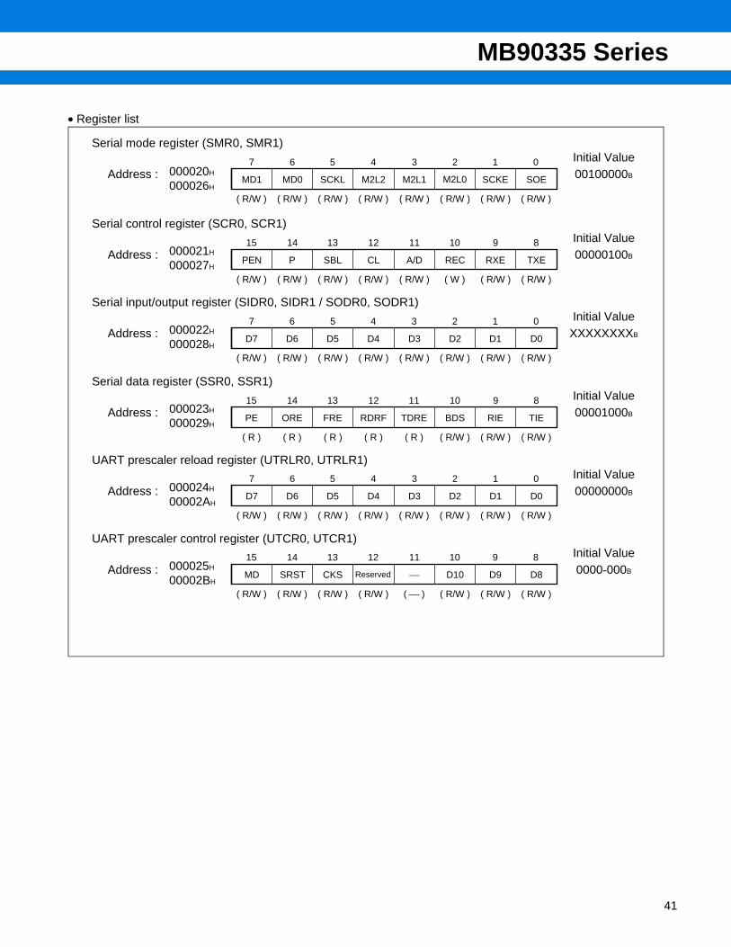
• Register list
Serial mode register (SMR0, SMR1)
Serial control register (SCR0, SCR1)
Serial input/output register (SIDR0, SIDR1 / SODR0, SODR1)
Serial data register (SSR0, SSR1)
UART prescaler reload register (UTRLR0, UTRLR1)
UART prescaler control register (UTCR0, UTCR1)
000020H
000026H
Initial ValueAddress : 00100000B
000021H
000027H
Initial ValueAddress : 00000100B
000022H
000028H
Initial ValueAddress : XXXXXXXXB
000023H
000029H
Initial ValueAddress : 00001000B
000024H
00002AH
Initial ValueAddress : 00000000B
000025H
00002BH
Initial ValueAddress : 0000-000B
( R/W ) ( R/W ) ( R/W ) ( R/W ) ( R/W ) ( R/W ) ( R/W )
7 6 5 4 3 2 1 0
MD0
( R/W )
MD1 SCKL M2L2 M2L1 SCKE SOEM2L0
( R/W ) ( R/W ) ( R/W ) ( R/W ) ( W ) ( R/W ) ( R/W )
15 14 13 12 11 10 9 8
P
( R/W )
PEN SBL CL A/D REC RXE TXE
( R/W ) ( R/W ) ( R/W ) ( R/W ) ( R/W ) ( R/W ) ( R/W )
7 6 5 4 3 2 1 0
D6
( R/W )
D7 D5 D4 D3 D2 D1 D0
( R ) ( R ) ( R ) ( R ) ( R/W ) ( R/W ) ( R/W )
15 14 13 12 11 10 9 8
ORE
( R )
PE FRE RDRF TDRE BDS RIE TIE
( R/W ) ( R/W ) ( R/W ) ( R/W ) ( R/W ) ( R/W ) ( R/W )
7 6 5 4 3 2 1 0
D6
( R/W )
D7 D5 D4 D3 D2 D1 D0
( R/W ) ( R/W ) ( R/W ) ( ⎯ ) ( R/W ) ( R/W ) ( R/W )
15 14 13 12 11 10 9 8
SRST
( R/W )
MD CKS ⎯ D10 D9 D8Reserved
41
MB90335 Series
42
• Block Diagram
MD1MD0SCKLM2L2M2L1M2L0SCKESOE
PENPSBLCLA/DRECRXETXE
PEOREFRERDRFTDREBDSRIETIE
SIDR0, SIDR1
SCK0, SCK1
SOT0, SOT1
#39 (27H)*
#37 (25H)*
SIN0, SIN1
SODR0, SODR1
SMR0,SMR1
SCR0,SCR1
SSR0,SSR1
Reception
complete
Control busSpecial-purpose baud-rate generator(UART prescaler control register UTCR0, UTCR1) (UART prescaler reload resister UTRLR0, UTRLR1)
Clock selector
Receive status decision circuit Reception error
occurrence signal for EI2OS (to CPU)
Reception clock
Reception control circuit
Start bit detection circuit
Reception bit counter
Reception parity counter
Shift register for reception
Internal data bus
Transmission clock
Reception interrupt signal
Transmission control circuit
Transmission start circuit
Transmission bit counter
Transmission parity counter
Shift register for transmission
Start transmission
* : Interrupt number
Send interrupt signal
Pin
Pin
Pin
MB90335 Series
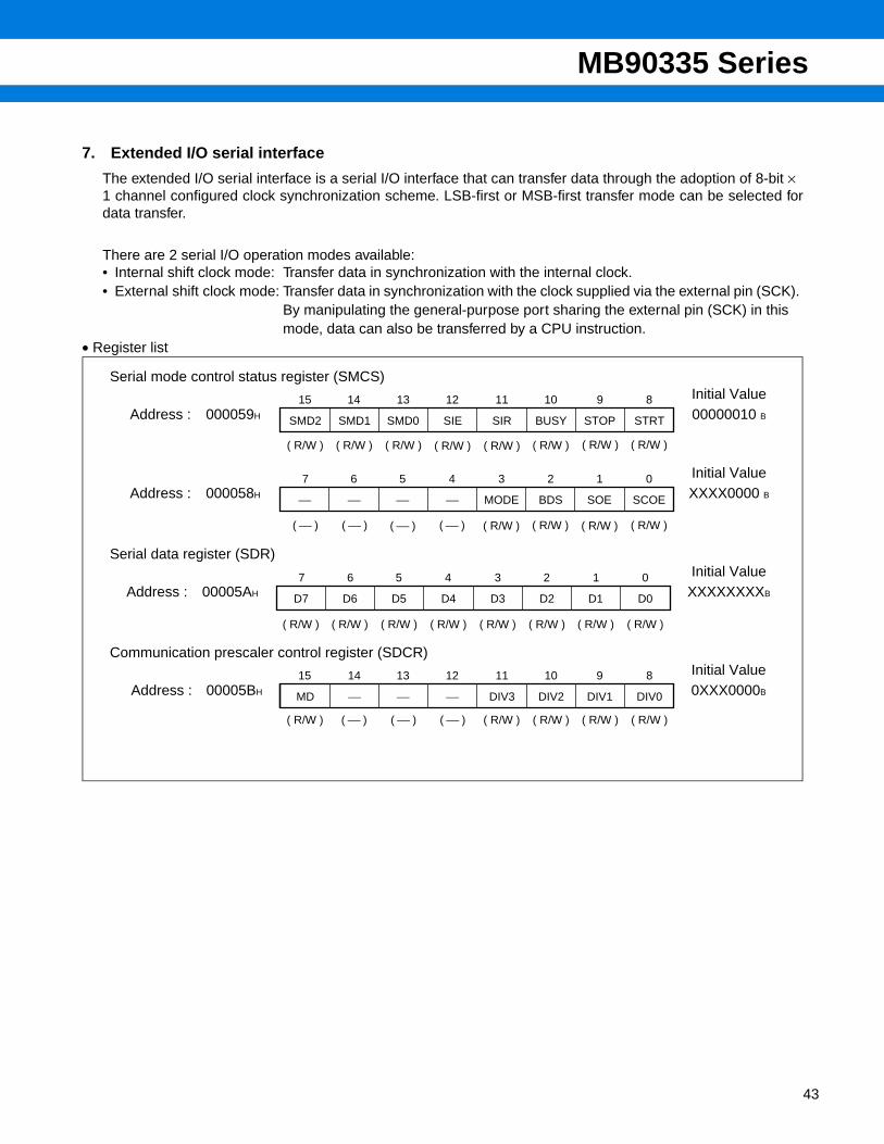
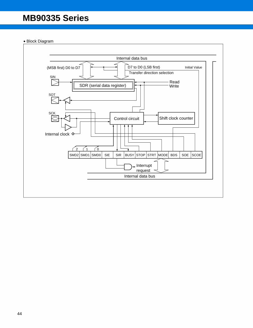
7. Extended I/O serial interface
The extended I/O serial interface is a serial I/O interface that can transfer data through the adoption of 8-bit × 1 channel configured clock synchronization scheme. LSB-first or MSB-first transfer mode can be selected fordata transfer.
There are 2 serial I/O operation modes available:• Internal shift clock mode: Transfer data in synchronization with the internal clock.• External shift clock mode: Transfer data in synchronization with the clock supplied via the external pin (SCK).
By manipulating the general-purpose port sharing the external pin (SCK) in this mode, data can also be transferred by a CPU instruction.
• Register list
Serial mode control status register (SMCS)
Serial data register (SDR)
Communication prescaler control register (SDCR)
Initial ValueAddress : 000059H 00000010 B
Initial ValueAddress : 000058H XXXX0000 B
Initial ValueAddress : 00005AH XXXXXXXXB
Initial ValueAddress : 00005BH 0XXX0000B
15 14 13 12 11 10 9 8
SMD1SMD2 SMD0 SIE SIR BUSY STOP STRT
( R/W ) ( R/W ) ( R/W ) ( R/W )( R/W )( R/W )( R/W )( R/W )
7 6 5 4 3 2 1 0
⎯⎯ ⎯ ⎯ MODE BDS SOE SCOE
( ⎯ ) ( ⎯ )( ⎯ )( ⎯ ) ( R/W ) ( R/W ) ( R/W ) ( R/W )
7 6 5 4 3 2 1 0
D6D7 D5 D4 D3 D2 D1 D0
( R/W ) ( R/W ) ( R/W ) ( R/W ) ( R/W )( R/W )( R/W )( R/W )
( ⎯ ) ( ⎯ ) ( ⎯ ) ( R/W ) ( R/W ) ( R/W ) ( R/W )
15 14 13 12 11 10 9 8
⎯
( R/W )
MD ⎯ ⎯ DIV3 DIV2 DIV1 DIV0
43
MB90335 Series
44
• Block Diagram
SIN
SOT
SCK
SMD2 SMD1 SMD0 SIE SIR BUSY STOP STRT MODE BDS
2 1 0
SOE SCOE
(MSB first) D0 to D7 D7 to D0 (LSB first)
SDR (serial data register)
Internal clock
Internal data bus
Transfer direction selection
ReadWrite
Control circuit Shift clock counter
Interrupt request
Internal data bus
Initial Value
MB90335 Series
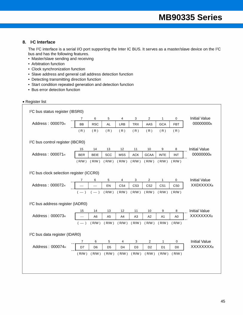
8. I2C Interface
The I2C interface is a serial I/O port supporting the Inter IC BUS. It serves as a master/slave device on the I2Cbus and has the following features.• Master/slave sending and receiving• Arbitration function• Clock synchronization function• Slave address and general call address detection function• Detecting transmitting direction function• Start condition repeated generation and detection function• Bus error detection function
• Register list
I2C bus status register (IBSR0)
I2C bus control register (IBCR0)
I2C bus clock selection register (ICCR0)
I2C bus address register (IADR0)
I2C bus data register (IDAR0)
Initial ValueAddress : 000070H 00000000B
Initial ValueAddress : 000071H 00000000B
Initial ValueAddress : 000072H XX0XXXXXB
Initial ValueAddress : 000073H XXXXXXXXB
Initial ValueAddress : 000074H XXXXXXXXB
( R ) ( R ) ( R ) ( R ) ( R ) ( R ) ( R )
7 6 5 4 3 2 1 0
RSC
( R )
BB AL LRB TRX AAS GCA FBT
( R/W ) ( R/W ) ( R/W ) ( R/W ) ( R/W ) ( R/W ) ( R/W )
15 14 13 12 11 10 9 8
BEIE
( R/W )
BER SCC MSS ACK GCAA INTE INT
( ⎯ ) ( R/W ) ( R/W ) ( R/W ) ( R/W ) ( R/W ) ( R/W )
7 6 5 4 3 2 1 0
⎯
( ⎯ )
⎯ EN CS4 CS3 CS2 CS1 CS0
( R/W ) ( R/W ) ( R/W ) ( R/W ) ( R/W ) ( R/W ) ( R/W )
15 14 13 12 11 10 9 8
A6
( ⎯ )
⎯ A5 A4 A3 A2 A1 A0
( R/W ) ( R/W ) ( R/W ) ( R/W ) ( R/W ) ( R/W ) ( R/W )
7 6 5 4 3 2 1 0
D6
( R/W )
D7 D5 D4 D3 D2 D1 D0
45
MB90335 Series
46
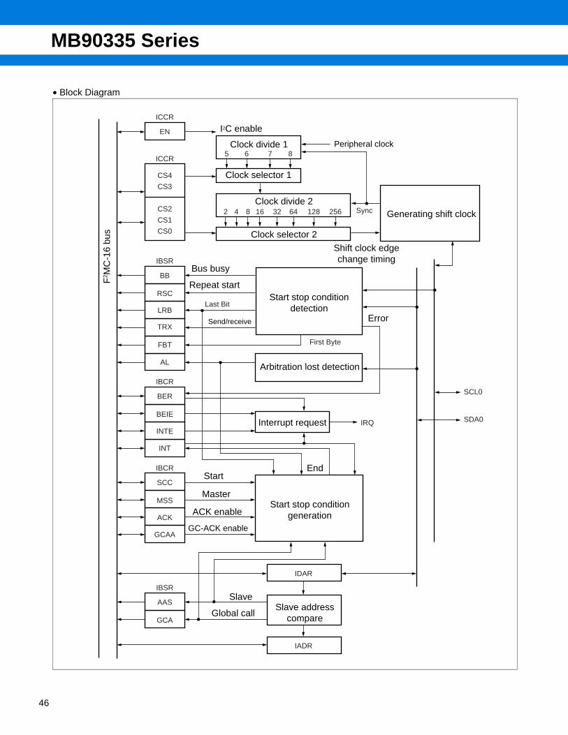
• Block Diagram
ICCR
EN
ICCR
IBSR
BB
RSC
LRBLast Bit
TRX
FBT
AL
IBCR
BER
BEIE
INTE
INT
IBCR
SCC
MSS
ACK
GCAA
IBSR
IDAR
IADR
AAS
GCA
CS4
CS3
CS2
CS1
CS0
2 4 8 16 128 25632 64
5 6 7 8
Sync
First Byte
IRQ
SCL0
SDA0
I2C enable
Clock divide 2
Clock selector 2
Bus busy
Repeat start
Send/receive
Start stop condition generation
Arbitration lost detection
Interrupt request
Start
Master
ACK enable
GC-ACK enable
SlaveSlave address
compare
End
Error
Shift clock edge change timing
Start stop condition detection
Generating shift clock
F2 M
C-1
6 bu
s
Clock divide 1
Clock selector 1
Peripheral clock
Global call
MB90335 Series
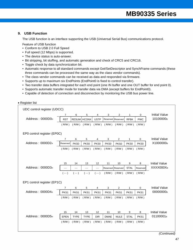
9. USB Function
The USB function is an interface supporting the USB (Universal Serial Bus) communications protocol.
Feature of USB function• Conform to USB 2.0 Full Speed• Full speed (12 Mbps) is supported.• The device status is auto-answer.• Bit stripping, bit stuffing, and automatic generation and check of CRC5 and CRC16.• Toggle check by data synchronization bit.• Automatic response to all standard commands except Get/SetDescriptor and SynchFrame commands (these
three commands can be processed the same way as the class vendor commands).• The class vendor commands can be received as data and responded via firmware.• Supports up to maximum six EndPoints (EndPoint0 is fixed to control transfer).• Two transfer data buffers integrated for each end point (one IN buffer and one OUT buffer for end point 0).• Supports automatic transfer mode for transfer data via DMA (except buffers for EndPoint0).• Capable of detection of connection and disconnection by monitoring the USB bus power line.
• Register list
(Continued)
UDC control register (UDCC)
EP0 control register (EP0C)
EP1 control register (EP1C)
Initial ValueAddress : 0000D0H 10100000B
Initial ValueAddress : 0000D2H X1000000B
Initial ValueAddress : 0000D3H XXXX000XB
Initial ValueAddress : 0000D4H 00000000B
Initial ValueAddress : 0000D5H 01100001B
( R/W ) ( R/W ) ( R/W ) ( R/W ) ( R/W ) ( R/W ) ( R/W )
7 6 5 4 3 2 1 0
RESUM
( R/W )
RST HCONX USTP RFBK PWCReserved Reserved
( R/W ) ( R/W ) ( R/W ) ( R/W ) ( R/W ) ( R/W ) ( R/W )
7 6 5 4 3 2 1 0
PKS0
( R/W )
PKS0 PKS0 PKS0 PKS0 PKS0PKS0Reserved
( ⎯ ) ( ⎯ ) ( ⎯ ) ( R/W ) ( R/W ) ( R/W ) ( R/W )
15 14 13 12 11 10 9 8
⎯
( ⎯ )
⎯ ⎯ ⎯ STALReserved Reserved Reserved
( R/W ) ( R/W ) ( R/W ) ( R/W ) ( R/W ) ( R/W ) ( R/W )
7 6 5 4 3 2 1 0
PKS1
( R/W )
PKS1 PKS1 PKS1 PKS1 PKS1 PKS1 PKS1
( R/W ) ( R/W ) ( R/W ) ( R/W ) ( R/W ) ( R/W ) ( R/W )
15 14 13 12 11 10 9 8
TYPE
( R/W )
EPEN TYPE DIR DMAE NULE STAL PKS1
47
MB90335 Series
48
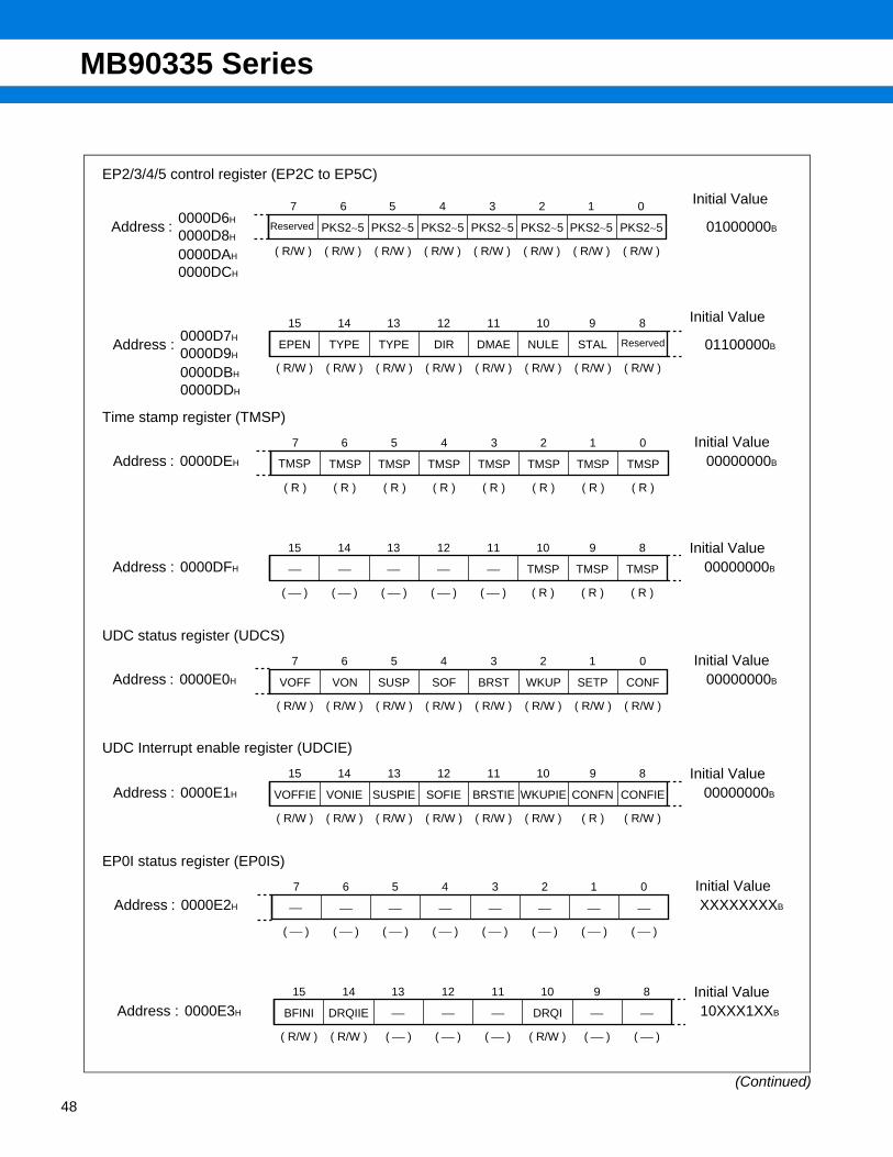
(Continued)
EP2/3/4/5 control register (EP2C to EP5C)
Time stamp register (TMSP)
UDC status register (UDCS)
UDC Interrupt enable register (UDCIE)
EP0I status register (EP0IS)
Initial Value
Address :0000D6H
0000D8H01000000B
0000DAH
0000DCH
Initial Value
Address :0000D7H
0000D9H01100000B
0000DBH
0000DDH
Initial ValueAddress : 0000DEH 00000000B
Initial ValueAddress : 0000DFH 00000000B
Initial ValueAddress : 0000E0H 00000000B
Initial ValueAddress : 0000E1H 00000000B
Initial ValueAddress : 0000E2H XXXXXXXXB
Initial ValueAddress : 0000E3H 10XXX1XXB
( R/W ) ( R/W ) ( R/W ) ( R/W ) ( R/W ) ( R/W ) ( R/W )
7 6 5 4 3 2 1 0
PKS2∼5
( R/W )
PKS2∼5 PKS2∼5 PKS2∼5 PKS2∼5 PKS2∼5 PKS2∼5Reserved
( R/W ) ( R/W ) ( R/W ) ( R/W ) ( R/W ) ( R/W ) ( R/W )
15 14 13 12 11 10 9 8
TYPE
( R/W )
EPEN TYPE DIR DMAE NULE STAL Reserved
( R ) ( R ) ( R ) ( R ) ( R ) ( R ) ( R )
7 6 5 4 3 2 1 0
TMSP
( R )
TMSP TMSP TMSP TMSP TMSP TMSPTMSP
( ⎯ ) ( ⎯ ) ( ⎯ ) ( ⎯ ) ( R ) ( R ) ( R )
15 14 13 12 11 10 9 8
⎯
( ⎯ )
⎯ ⎯ ⎯ ⎯ TMSP TMSP TMSP
( R/W ) ( R/W ) ( R/W ) ( R/W ) ( R/W ) ( R/W ) ( R/W )
7 6 5 4 3 2 1 0
VON
( R/W )
VOFF SUSP SOF BRST WKUP SETP CONF
( R/W ) ( R/W ) ( R/W ) ( R/W ) ( R/W ) ( R ) ( R/W )
15 14 13 12 11 10 9 8
VONIE
( R/W )
VOFFIE SUSPIE SOFIE BRSTIE WKUPIE CONFN CONFIE
( ⎯ ) ( ⎯ ) ( ⎯ ) ( ⎯ ) ( ⎯ ) ( ⎯ ) ( ⎯ )
7 6 5 4 3 2 1 0
⎯
( ⎯ )
⎯ ⎯ ⎯ ⎯ ⎯ ⎯⎯
( R/W ) ( ⎯ ) ( ⎯ ) ( ⎯ ) ( R/W ) ( ⎯ ) ( ⎯ )
15 14 13 12 11 10 9 8
DRQIIE
( R/W )
BFINI ⎯ ⎯ ⎯ DRQI ⎯ ⎯
MB90335 Series
(Continued)
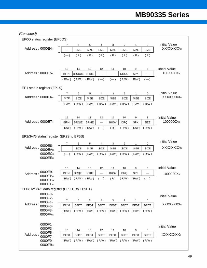
EP0O status register (EP0OS)
EP1 status register (EP1S)
EP2/3/4/5 status register (EP2S to EP5S)
EP0/1/2/3/4/5 data register (EP0DT to EP5DT)
Initial ValueAddress : 0000E4H XXXXXXXXB
Initial ValueAddress : 0000E5H 100XX00XB
Initial ValueAddress : 0000E6H XXXXXXXXB
Initial ValueAddress : 0000E7H 1000000XB
Initial Value
Address :0000E8H
0000EAHXXXXXXXXB
0000ECH
0000EEH
Initial Value
Address :0000E9H
0000EBH1000000XB
0000EDH
0000EFH
0000F0H
0000F2HInitial Value
Address :0000F4H
0000F6HXXXXXXXXB
0000F8H
0000FAH
0000F1H
0000F3HInitial Value
Address :0000F5H
0000F7HXXXXXXXXB
0000F9H
0000FBH
( R ) ( R ) ( R ) ( R ) ( R ) ( R ) ( R )
7 6 5 4 3 2 1 0
SIZE
( ⎯ )
⎯ SIZE SIZE SIZE SIZE SIZE SIZE
( R/W ) ( R/W ) ( ⎯ ) ( ⎯ ) ( R/W ) ( R/W ) ( ⎯ )
15 14 13 12 11 10 9 8
DRQOIE
( R/W )
BFINI SPKIE ⎯ ⎯ DRQO SPK ⎯
( R/W ) ( R/W ) ( R/W ) ( R/W ) ( R/W ) ( R/W ) ( R/W )
7 6 5 4 3 2 1 0
SIZE
( R/W )
SIZE SIZE SIZE SIZE SIZE SIZESIZE
( R/W ) ( R/W ) ( ⎯ ) ( R ) ( R/W ) ( R/W ) ( R/W )
15 14 13 12 11 10 9 8
DRQIE
( R/W )
BFINI SPKIE ⎯ BUSY DRQ SPK SIZE
( R/W ) ( R/W ) ( R/W ) ( R/W ) ( R/W ) ( R/W ) ( R/W )
7 6 5 4 3 2 1 0
SIZE
( ⎯ )
⎯ SIZE SIZE SIZE SIZE SIZE SIZE
( R/W ) ( R/W ) ( ⎯ ) ( R ) ( R/W ) ( R/W ) ( ⎯ )
15 14 13 12 11 10 9 8
DRQIE
( R/W )
BFINI SPKIE ⎯ BUSY DRQ SPK ⎯
( R/W ) ( R/W ) ( R/W ) ( R/W ) ( R/W ) ( R/W ) ( R/W )
7 6 5 4 3 2 1 0
BFDT
( R/W )
BFDT BFDT BFDT BFDT BFDT BFDTBFDT
( R/W ) ( R/W ) ( R/W ) ( R/W ) ( R/W ) ( R/W ) ( R/W )
15 14 13 12 11 10 9 8
BFDT
( R/W )
BFDT BFDT BFDT BFDT BFDT BFDT BFDT
49
MB90335 Series
50
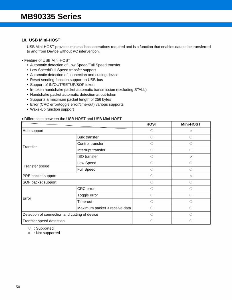
10. USB Mini-HOST
USB Mini-HOST provides minimal host operations required and is a function that enables data to be transferredto and from Device without PC intervention.
• Feature of USB Mini-HOST• Automatic detection of Low Speed/Full Speed transfer• Low Speed/Full Speed transfer support• Automatic detection of connection and cutting device• Reset sending function support to USB-bus• Support of IN/OUT/SETUP/SOF token• In-token handshake packet automatic transmission (excluding STALL)• Handshake packet automatic detection at out-token• Supports a maximum packet length of 256 bytes• Error (CRC error/toggle error/time-out) various supports• Wake-Up function support
• Differences between the USB HOST and USB Mini-HOST
: Supported × : Not supported
HOST Mini-HOST
Hub support ×
Transfer
Bulk transfer
Control transfer
Interrupt transfer
ISO transfer ×
Transfer speedLow Speed
Full Speed
PRE packet support ×
SOF packet support
Error
CRC error
Toggle error
Time-out
Maximum packet < receive data
Detection of connection and cutting of device
Transfer speed detection
MB90335 Series
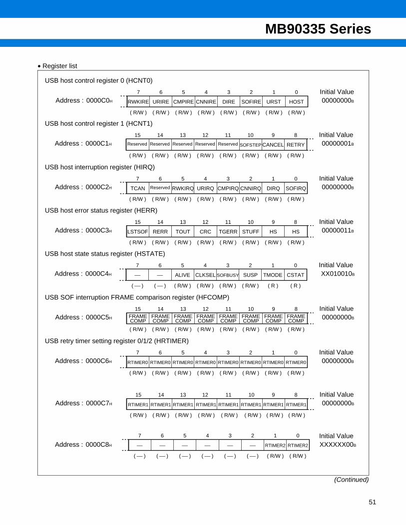
• Register list
(Continued)
USB host control register 0 (HCNT0)
USB host control register 1 (HCNT1)
USB host interruption register (HIRQ)
USB host error status register (HERR)
USB host state status register (HSTATE)
USB SOF interruption FRAME comparison register (HFCOMP)
USB retry timer setting register 0/1/2 (HRTIMER)
Initial ValueAddress : 0000C0H 00000000B
Initial ValueAddress : 0000C1H 00000001B
Initial ValueAddress : 0000C2H 00000000B
Initial ValueAddress : 0000C3H 00000011B
Initial ValueAddress : 0000C4H XX010010B
Initial ValueAddress : 0000C5H 00000000B
Initial ValueAddress : 0000C6H 00000000B
Initial ValueAddress : 0000C7H 00000000B
Initial ValueAddress : 0000C8H XXXXXX00B
( R/W ) ( R/W ) ( R/W ) ( R/W ) ( R/W ) ( R/W ) ( R/W )
7 6 5 4 3 2 1 0
URIRE
( R/W )
RWKIRE CMPIRE CNNIRE DIRE SOFIRE URST HOST
( R/W ) ( R/W ) ( R/W ) ( R/W ) ( R/W ) ( R/W ) ( R/W )
15 14 13 12 11 10 9 8
( R/W )
SOFSTEP CANCEL RETRYReserved Reserved Reserved Reserved Reserved
( R/W ) ( R/W ) ( R/W ) ( R/W ) ( R/W ) ( R/W ) ( R/W )
7 6 5 4 3 2 1 0
( R/W )
TCAN RWKIRQ URIRQ CMPIRQ CNNIRQ DIRQ SOFIRQReserved
( R/W ) ( R/W ) ( R/W ) ( R/W ) ( R/W ) ( R/W ) ( R/W )
15 14 13 12 11 10 9 8
RERR
( R/W )
LSTSOF TOUT CRC TGERR STUFF HS HS
( ⎯ ) ( R/W ) ( R/W ) ( R/W ) ( R/W ) ( R ) ( R )
7 6 5 4 3 2 1 0
⎯
( ⎯ )
⎯ ALIVE CLKSEL SOFBUSY SUSP TMODE CSTAT
( R/W ) ( R/W ) ( R/W ) ( R/W ) ( R/W ) ( R/W ) ( R/W )
15 14 13 12 11 10 9 8
( R/W )
FRAMECOMP
FRAMECOMP
FRAMECOMP
FRAMECOMP
FRAMECOMP
FRAMECOMP
FRAMECOMP
FRAMECOMP
( R/W ) ( R/W ) ( R/W ) ( R/W ) ( R/W ) ( R/W ) ( R/W )
7 6 5 4 3 2 1 0
RTIMER0
( R/W )
RTIMER0 RTIMER0 RTIMER0 RTIMER0 RTIMER0 RTIMER0 RTIMER0
( R/W ) ( R/W ) ( R/W ) ( R/W ) ( R/W ) ( R/W ) ( R/W )
15 14 13 12 11 10 9 8
RTIMER1
( R/W )
RTIMER1 RTIMER1 RTIMER1 RTIMER1 RTIMER1 RTIMER1 RTIMER1
( ⎯ ) ( ⎯ ) ( ⎯ ) ( ⎯ ) ( ⎯ ) ( R/W ) ( R/W )
7 6 5 4 3 2 1 0
⎯
( ⎯ )
⎯ ⎯ ⎯ ⎯ ⎯ RTIMER2 RTIMER2
51
MB90335 Series
52
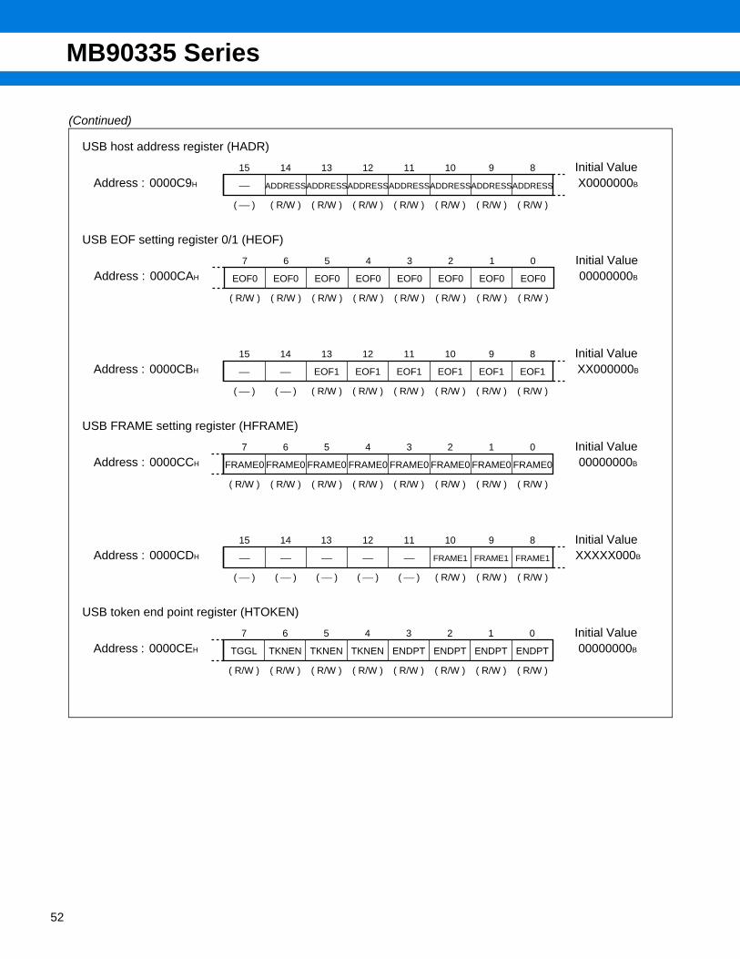
(Continued)
USB host address register (HADR)
USB EOF setting register 0/1 (HEOF)
USB FRAME setting register (HFRAME)
USB token end point register (HTOKEN)
Initial ValueAddress : 0000C9H X0000000B
Initial ValueAddress : 0000CAH 00000000B
Initial ValueAddress : 0000CBH XX000000B
Initial ValueAddress : 0000CCH 00000000B
Initial ValueAddress : 0000CDH XXXXX000B
Initial ValueAddress : 0000CEH 00000000B
( R/W ) ( R/W ) ( R/W ) ( R/W ) ( R/W ) ( R/W ) ( R/W )
15 14 13 12 11 10 9 8
ADDRESS
( ⎯ )
⎯ ADDRESSADDRESSADDRESSADDRESSADDRESSADDRESS
( R/W ) ( R/W ) ( R/W ) ( R/W ) ( R/W ) ( R/W ) ( R/W )
7 6 5 4 3 2 1 0
EOF0
( R/W )
EOF0 EOF0 EOF0 EOF0 EOF0 EOF0 EOF0
( ⎯ ) ( R/W ) ( R/W ) ( R/W ) ( R/W ) ( R/W ) ( R/W )
15 14 13 12 11 10 9 8
⎯
( ⎯ )
⎯ EOF1 EOF1 EOF1 EOF1 EOF1 EOF1
( R/W ) ( R/W ) ( R/W ) ( R/W ) ( R/W ) ( R/W ) ( R/W )
7 6 5 4 3 2 1 0
FRAME0
( R/W )
FRAME0 FRAME0 FRAME0 FRAME0 FRAME0 FRAME0 FRAME0
( ⎯ ) ( ⎯ ) ( ⎯ ) ( ⎯ ) ( R/W ) ( R/W ) ( R/W )
15 14 13 12 11 10 9 8
⎯
( ⎯ )
⎯ ⎯ ⎯ ⎯ FRAME1 FRAME1 FRAME1
( R/W ) ( R/W ) ( R/W ) ( R/W ) ( R/W ) ( R/W ) ( R/W )
7 6 5 4 3 2 1 0
TKNEN
( R/W )
TGGL TKNEN TKNEN ENDPT ENDPT ENDPT ENDPT
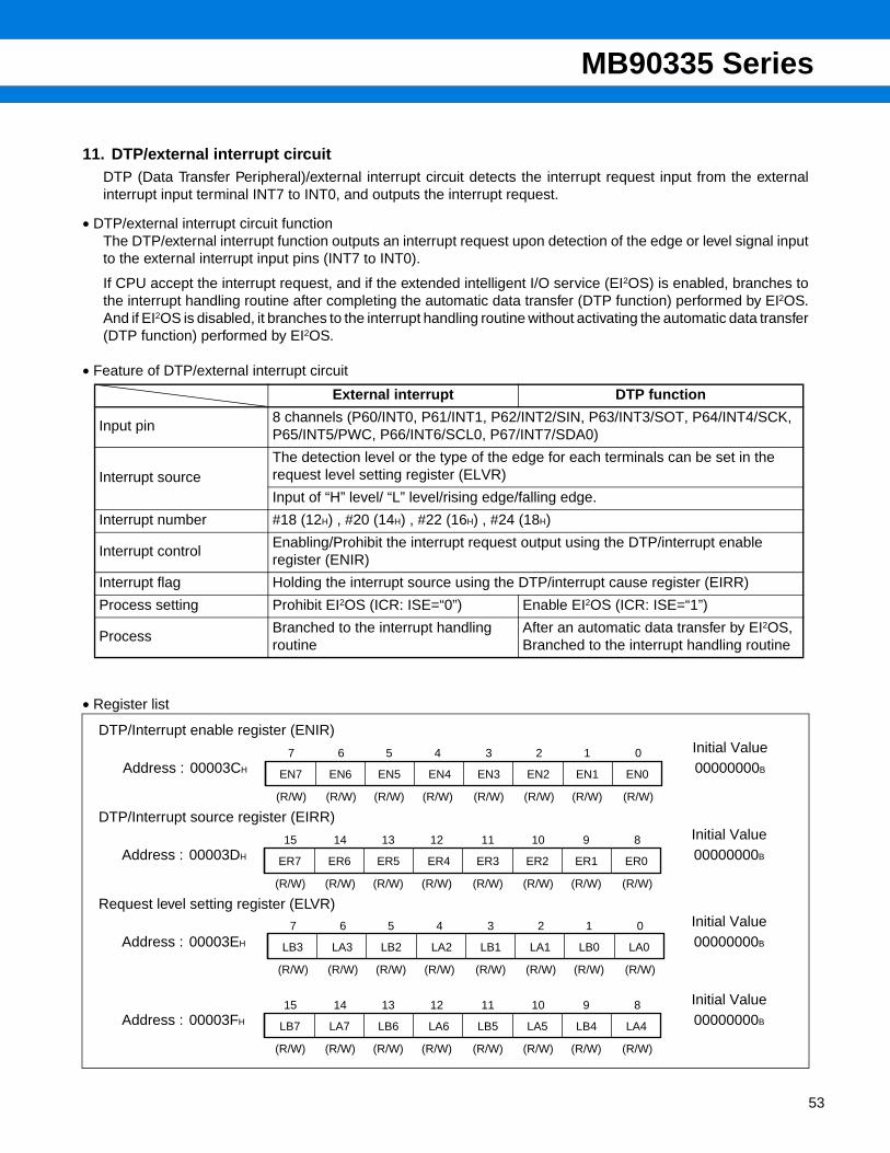
MB90335 Series
11. DTP/external interrupt circuitDTP (Data Transfer Peripheral)/external interrupt circuit detects the interrupt request input from the externalinterrupt input terminal INT7 to INT0, and outputs the interrupt request.
• DTP/external interrupt circuit functionThe DTP/external interrupt function outputs an interrupt request upon detection of the edge or level signal inputto the external interrupt input pins (INT7 to INT0).
If CPU accept the interrupt request, and if the extended intelligent I/O service (EI2OS) is enabled, branches tothe interrupt handling routine after completing the automatic data transfer (DTP function) performed by EI2OS.And if EI2OS is disabled, it branches to the interrupt handling routine without activating the automatic data transfer(DTP function) performed by EI2OS.
• Feature of DTP/external interrupt circuit
• Register list
External interrupt DTP function
Input pin8 channels (P60/INT0, P61/INT1, P62/INT2/SIN, P63/INT3/SOT, P64/INT4/SCK, P65/INT5/PWC, P66/INT6/SCL0, P67/INT7/SDA0)
Interrupt sourceThe detection level or the type of the edge for each terminals can be set in the request level setting register (ELVR)
Input of “H” level/ “L” level/rising edge/falling edge.
Interrupt number #18 (12H) , #20 (14H) , #22 (16H) , #24 (18H)
Interrupt controlEnabling/Prohibit the interrupt request output using the DTP/interrupt enable register (ENIR)
Interrupt flag Holding the interrupt source using the DTP/interrupt cause register (EIRR)
Process setting Prohibit EI2OS (ICR: ISE=“0”) Enable EI2OS (ICR: ISE=“1”)
ProcessBranched to the interrupt handling routine
After an automatic data transfer by EI2OS, Branched to the interrupt handling routine
DTP/Interrupt enable register (ENIR)
DTP/Interrupt source register (EIRR)
Request level setting register (ELVR)
Initial ValueAddress : 00003CH 00000000B
Initial ValueAddress : 00003DH 00000000B
Initial ValueAddress : 00003EH 00000000B
Initial ValueAddress : 00003FH 00000000B
7 6 5 4 3 2 1 0
(R/W) (R/W) (R/W) (R/W) (R/W) (R/W) (R/W) (R/W)
EN6EN7 EN5 EN4 EN3 EN2 EN1 EN0
15 14 13 12 11 10 9 8
(R/W) (R/W) (R/W) (R/W) (R/W) (R/W) (R/W) (R/W)
ER6ER7 ER5 ER4 ER3 ER2 ER1 ER0
7 6 5 4 3 2 1 0
(R/W) (R/W) (R/W) (R/W) (R/W) (R/W) (R/W) (R/W)
LA3LB3 LB2 LA2 LB1 LA1 LB0 LA0
15 14 13 12 11 10 9 8
(R/W) (R/W) (R/W) (R/W) (R/W) (R/W) (R/W) (R/W)
LA7LB7 LB6 LA6 LB5 LA5 LB4 LA4
53
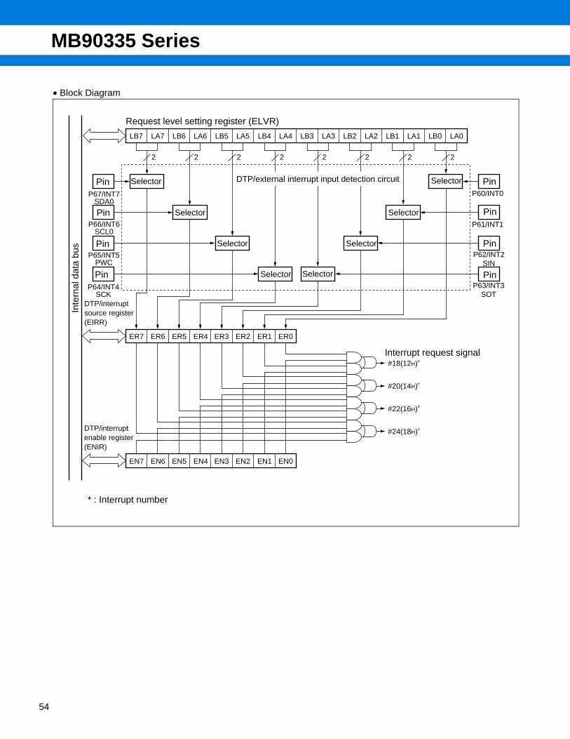
MB90335 Series
54
• Block Diagram
LB7
ER7 ER6 ER5 ER4 ER3 ER2 ER1 ER0
EN7 EN6 EN5 EN4 EN3 EN2 EN1 EN0
P60/INT0
LA7 LB6 LA6 LB5 LA5 LB4 LA4 LB3 LA3 LB2 LA2 LB1 LA1 LB0 LA0
P61/INT1
P62/INT2SIN
P63/INT3SOT
#18(12H)*
#20(14H)*
#22(16H)*
#24(18H)*
2 2 2 2 2 2 2 2
P64/INT4SCK
P65/INT5PWC
P66/INT6SCL0
P67/INT7SDA0
Request level setting register (ELVR)
Pin
Pin
Pin
Pin
Selector
Selector
Selector
Selector Selector
Selector
Selector
Selector Pin
Pin
Pin
Pin
Interrupt request signal
Inte
rnal
dat
a bu
s
DTP/interrupt source register (EIRR)
DTP/interrupt enable register (ENIR)
* : Interrupt number
DTP/external interrupt input detection circuit
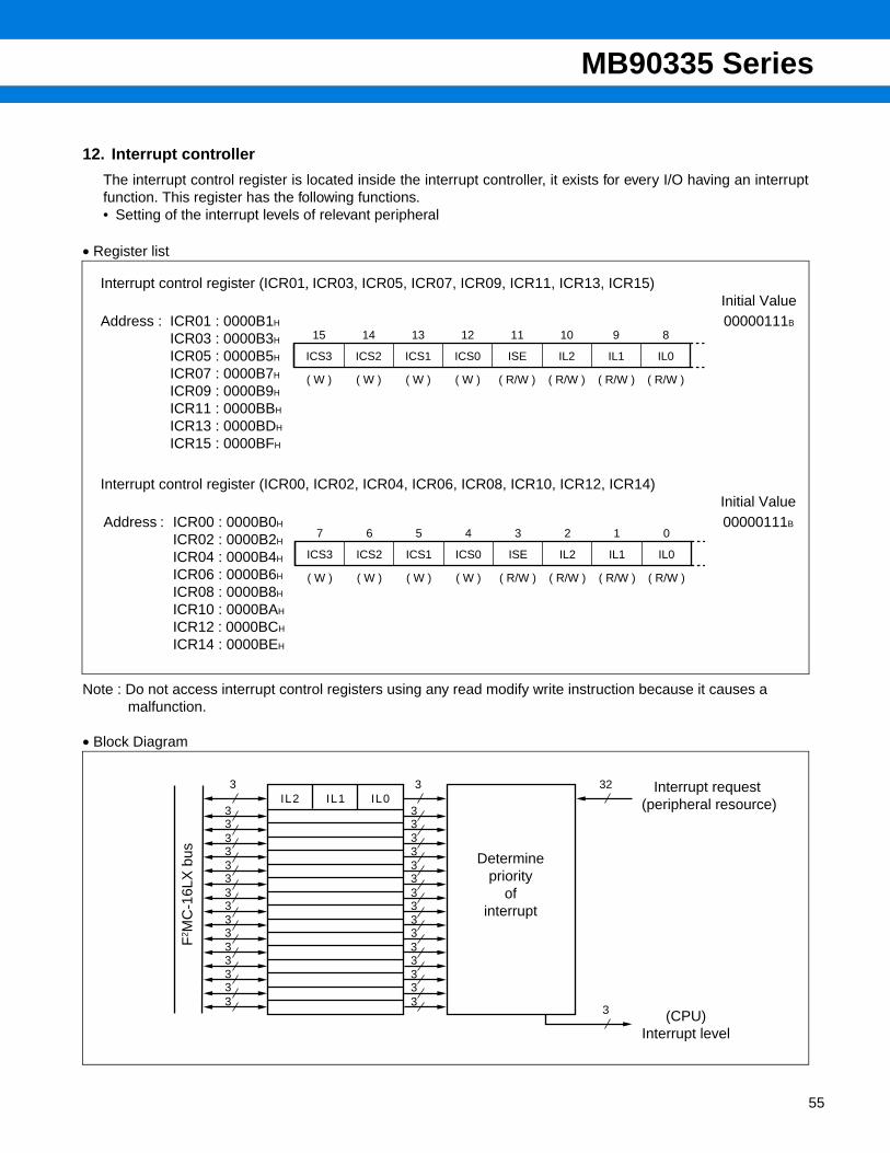
MB90335 Series
12. Interrupt controller
The interrupt control register is located inside the interrupt controller, it exists for every I/O having an interruptfunction. This register has the following functions.• Setting of the interrupt levels of relevant peripheral
• Register list
Note : Do not access interrupt control registers using any read modify write instruction because it causes a malfunction.
• Block Diagram
Interrupt control register (ICR01, ICR03, ICR05, ICR07, ICR09, ICR11, ICR13, ICR15)
Interrupt control register (ICR00, ICR02, ICR04, ICR06, ICR08, ICR10, ICR12, ICR14)
Initial ValueAddress : ICR01 : 0000B1H
ICR03 : 0000B3H
ICR05 : 0000B5H
ICR07 : 0000B7H
ICR09 : 0000B9H
ICR11 : 0000BBH
ICR13 : 0000BDH
ICR15 : 0000BFH
00000111B
Initial ValueAddress : ICR00 : 0000B0H
ICR02 : 0000B2H
ICR04 : 0000B4H
ICR06 : 0000B6H
ICR08 : 0000B8H
ICR10 : 0000BAH
ICR12 : 0000BCH
ICR14 : 0000BEH
00000111B
( W ) ( W ) ( W ) ( R/W ) ( R/W ) ( R/W ) ( R/W )
15 14 13 12 11 10 9 8
ICS2
( W )
ICS3 ICS1 ICS0 ISE IL2 IL1 IL0
( W ) ( W ) ( W ) ( R/W ) ( R/W ) ( R/W ) ( R/W )
7 6 5 4 3 2 1 0
ICS2
( W )
ICS3 ICS1 ICS0 ISE IL2 IL1 IL0
IL2 IL1 IL032
3
3
3333333333
33
333
3
3333333333
33
333
Determinepriority
ofinterrupt
Interrupt request (peripheral resource)
(CPU) Interrupt level
F2 M
C-1
6LX
bus
55
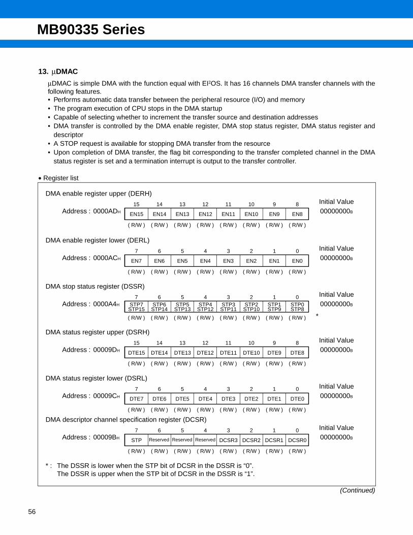
MB90335 Series
56
13. µDMAC
µDMAC is simple DMA with the function equal with EI2OS. It has 16 channels DMA transfer channels with thefollowing features.• Performs automatic data transfer between the peripheral resource (I/O) and memory• The program execution of CPU stops in the DMA startup• Capable of selecting whether to increment the transfer source and destination addresses• DMA transfer is controlled by the DMA enable register, DMA stop status register, DMA status register and
descriptor• A STOP request is available for stopping DMA transfer from the resource• Upon completion of DMA transfer, the flag bit corresponding to the transfer completed channel in the DMA
status register is set and a termination interrupt is output to the transfer controller.
• Register list
(Continued)
DMA enable register upper (DERH)
DMA enable register lower (DERL)
DMA stop status register (DSSR)
DMA status register upper (DSRH)
DMA status register lower (DSRL)
DMA descriptor channel specification register (DCSR)
* : The DSSR is lower when the STP bit of DCSR in the DSSR is “0”. The DSSR is upper when the STP bit of DCSR in the DSSR is “1”.
Initial ValueAddress : 0000ADH 00000000B
Initial ValueAddress : 0000ACH 00000000B
Initial ValueAddress : 0000A4H 00000000B
*
Initial ValueAddress : 00009DH 00000000B
Initial ValueAddress : 00009CH 00000000B
Initial ValueAddress : 00009BH 00000000B
( R/W ) ( R/W ) ( R/W ) ( R/W ) ( R/W ) ( R/W ) ( R/W )
15 14 13 12 11 10 9 8
EN14
( R/W )
EN15 EN13 EN12 EN11 EN10 EN9 EN8
( R/W ) ( R/W ) ( R/W ) ( R/W ) ( R/W ) ( R/W ) ( R/W )
7 6 5 4 3 2 1 0
EN6
( R/W )
EN7 EN5 EN4 EN3 EN2 EN1 EN0
7 6 5 4 3 2 1 0STP6
STP14STP7
STP15STP5
STP13STP4
STP12STP3
STP11STP2
STP10STP1STP9
STP0STP8
( R/W ) ( R/W ) ( R/W ) ( R/W ) ( R/W ) ( R/W ) ( R/W )( R/W )
15 14 13 12 11 10 9 8
DTE14DTE15 DTE13 DTE12 DTE11 DTE10 DTE9 DTE8
( R/W ) ( R/W ) ( R/W ) ( R/W ) ( R/W ) ( R/W ) ( R/W )( R/W )
( R/W ) ( R/W ) ( R/W ) ( R/W ) ( R/W ) ( R/W ) ( R/W )
7 6 5 4 3 2 1 0
DTE6
( R/W )
DTE7 DTE5 DTE4 DTE3 DTE2 DTE1 DTE0
( R/W ) ( R/W ) ( R/W ) ( R/W ) ( R/W ) ( R/W ) ( R/W )
7 6 5 4 3 2 1 0
( R/W )
STP DCSR3 DCSR2 DCSR1 DCSR0Reserved Reserved Reserved
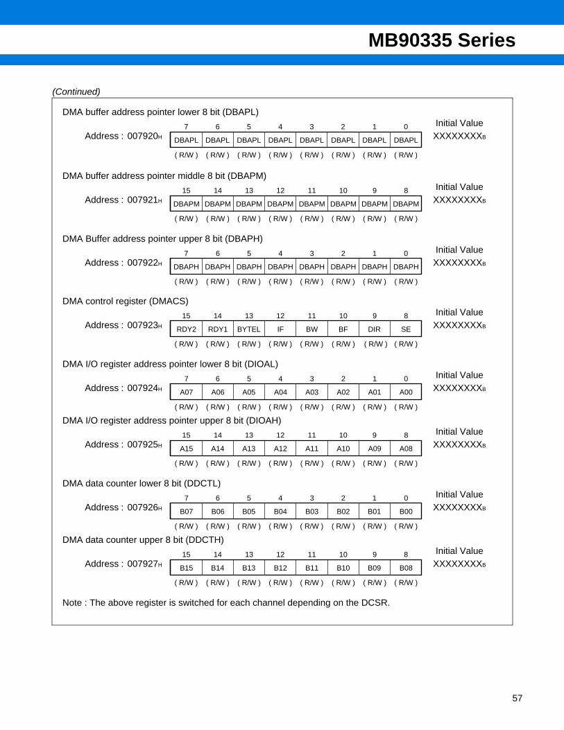
MB90335 Series
(Continued)
DMA buffer address pointer lower 8 bit (DBAPL)
DMA buffer address pointer middle 8 bit (DBAPM)
DMA Buffer address pointer upper 8 bit (DBAPH)
DMA control register (DMACS)
DMA I/O register address pointer lower 8 bit (DIOAL)
DMA I/O register address pointer upper 8 bit (DIOAH)
DMA data counter lower 8 bit (DDCTL)
DMA data counter upper 8 bit (DDCTH)
Note : The above register is switched for each channel depending on the DCSR.
Initial ValueAddress : 007920H XXXXXXXXB
Initial ValueAddress : 007921H XXXXXXXXB
Initial ValueAddress : 007922H XXXXXXXXB
Initial ValueAddress : 007923H XXXXXXXXB
Initial ValueAddress : 007924H XXXXXXXXB
Initial ValueAddress : 007925H XXXXXXXXB
Initial ValueAddress : 007926H XXXXXXXXB
Initial ValueAddress : 007927H XXXXXXXXB
( R/W ) ( R/W ) ( R/W ) ( R/W ) ( R/W ) ( R/W ) ( R/W )
7 6 5 4 3 2 1 0
DBAPL
( R/W )
DBAPL DBAPL DBAPL DBAPL DBAPL DBAPL DBAPL
15 14 13 12 11 10 9 8
DBAPMDBAPM DBAPM DBAPM DBAPM DBAPM DBAPM DBAPM
( R/W ) ( R/W ) ( R/W ) ( R/W ) ( R/W ) ( R/W ) ( R/W )( R/W )
7 6 5 4 3 2 1 0
DBAPHDBAPH DBAPH DBAPH DBAPH DBAPH DBAPH DBAPH
( R/W ) ( R/W ) ( R/W ) ( R/W ) ( R/W ) ( R/W ) ( R/W )( R/W )
15 14 13 12 11 10 9 8
RDY1RDY2 BYTEL IF BW BF DIR SE
( R/W ) ( R/W ) ( R/W ) ( R/W ) ( R/W ) ( R/W ) ( R/W )( R/W )
( R/W ) ( R/W ) ( R/W ) ( R/W ) ( R/W ) ( R/W ) ( R/W )
7 6 5 4 3 2 1 0
A06
( R/W )
A07 A05 A04 A03 A02 A01 A00
15 14 13 12 11 10 9 8
A14A15 A13 A12 A11 A10 A09 A08
( R/W ) ( R/W ) ( R/W ) ( R/W ) ( R/W ) ( R/W ) ( R/W )( R/W )
7 6 5 4 3 2 1 0
B06B07 B05 B04 B03 B02 B01 B00
( R/W ) ( R/W ) ( R/W ) ( R/W ) ( R/W ) ( R/W ) ( R/W )( R/W )
15 14 13 12 11 10 9 8
B14B15 B13 B12 B11 B10 B09 B08
( R/W ) ( R/W ) ( R/W ) ( R/W ) ( R/W ) ( R/W ) ( R/W )( R/W )
57
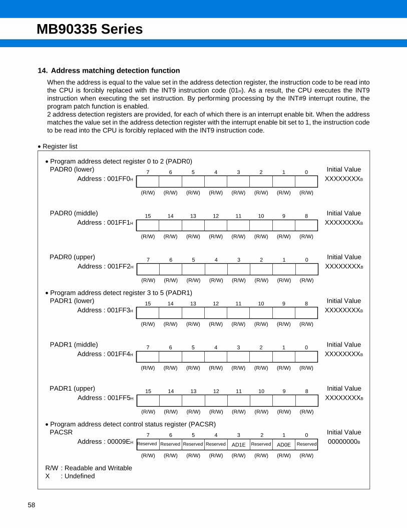
MB90335 Series
58
14. Address matching detection function
When the address is equal to the value set in the address detection register, the instruction code to be read intothe CPU is forcibly replaced with the INT9 instruction code (01H). As a result, the CPU executes the INT9instruction when executing the set instruction. By performing processing by the INT#9 interrupt routine, theprogram patch function is enabled.2 address detection registers are provided, for each of which there is an interrupt enable bit. When the addressmatches the value set in the address detection register with the interrupt enable bit set to 1, the instruction codeto be read into the CPU is forcibly replaced with the INT9 instruction code.
• Register list
• Program address detect register 0 to 2 (PADR0)
• Program address detect register 3 to 5 (PADR1)
• Program address detect control status register (PACSR)
R/W : Readable and WritableX : Undefined
PADR0 (lower) Initial ValueAddress : 001FF0H XXXXXXXXB
PADR0 (middle) Initial ValueAddress : 001FF1H XXXXXXXXB
PADR0 (upper) Initial ValueAddress : 001FF2H XXXXXXXXB
PADR1 (lower) Initial ValueAddress : 001FF3H XXXXXXXXB
PADR1 (middle) Initial ValueAddress : 001FF4H XXXXXXXXB
PADR1 (upper) Initial ValueAddress : 001FF5H XXXXXXXXB
PACSR Initial ValueAddress : 00009EH 00000000B
(R/W) (R/W) (R/W) (R/W) (R/W) (R/W) (R/W)
7 6 5 4 3 2 1 0
(R/W)
(R/W) (R/W) (R/W) (R/W) (R/W) (R/W) (R/W)
15 14 13 12 11 10 9 8
(R/W)
(R/W) (R/W) (R/W) (R/W) (R/W) (R/W) (R/W)
7 6 5 4 3 2 1 0
(R/W)
(R/W) (R/W) (R/W) (R/W) (R/W) (R/W) (R/W)
15 14 13 12 11 10 9 8
(R/W)
(R/W) (R/W) (R/W) (R/W) (R/W) (R/W) (R/W)
7 6 5 4 3 2 1 0
(R/W)
(R/W) (R/W) (R/W) (R/W) (R/W) (R/W) (R/W)
15 14 13 12 11 10 9 8
(R/W)
(R/W) (R/W) (R/W) (R/W) (R/W) (R/W) (R/W)
7 6 5 4 3 2 1 0
(R/W)
AD1E AD0EReserved Reserved Reserved Reserved Reserved Reserved
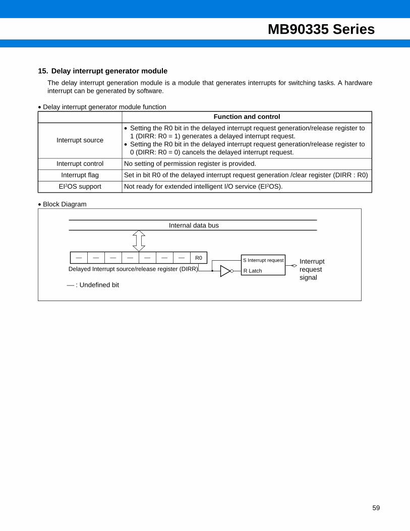
MB90335 Series
15. Delay interrupt generator module
The delay interrupt generation module is a module that generates interrupts for switching tasks. A hardwareinterrupt can be generated by software.
• Delay interrupt generator module function
• Block Diagram
Function and control
Interrupt source
• Setting the R0 bit in the delayed interrupt request generation/release register to 1 (DIRR: R0 = 1) generates a delayed interrupt request.
• Setting the R0 bit in the delayed interrupt request generation/release register to 0 (DIRR: R0 = 0) cancels the delayed interrupt request.
Interrupt control No setting of permission register is provided.
Interrupt flag Set in bit R0 of the delayed interrupt request generation /clear register (DIRR : R0)
EI2OS support Not ready for extended intelligent I/O service (EI2OS).
⎯ ⎯ ⎯ ⎯ ⎯ ⎯ ⎯ R0
Internal data bus
Delayed Interrupt source/release register (DIRR)
S Interrupt request
R Latch
⎯ : Undefined bit
Interrupt request signal
59
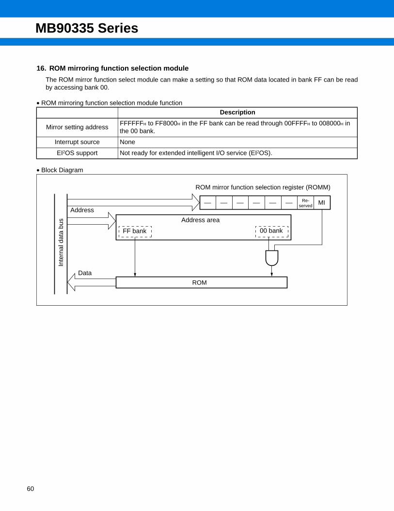
MB90335 Series
60
16. ROM mirroring function selection module
The ROM mirror function select module can make a setting so that ROM data located in bank FF can be readby accessing bank 00.
• ROM mirroring function selection module function
• Block Diagram
Description
Mirror setting addressFFFFFFH to FF8000H in the FF bank can be read through 00FFFFH to 008000H in the 00 bank.
Interrupt source None
EI2OS support Not ready for extended intelligent I/O service (EI2OS).
⎯ ⎯ ⎯ ⎯ ⎯ ⎯ MI
ROM
Inte
rnal
dat
a bu
s
ROM mirror function selection register (ROMM)
00 bankFF bank
Address
Data
Address area
Re-served
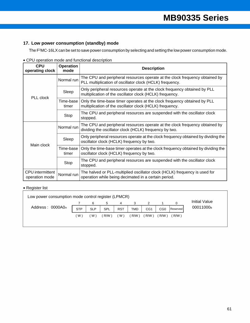
MB90335 Series
17. Low power consumption (standby) mode
The F2MC-16LX can be set to save power consumption by selecting and setting the low power consumption mode.
• CPU operation mode and functional description
• Register list
CPU operating clock
Operation mode Description
PLL clock
Normal runThe CPU and peripheral resources operate at the clock frequency obtained by PLL multiplication of oscillator clock (HCLK) frequency.
SleepOnly peripheral resources operate at the clock frequency obtained by PLL multiplication of the oscillator clock (HCLK) frequency.
Time-base timer
Only the time-base timer operates at the clock frequency obtained by PLL multiplication of the oscillator clock (HCLK) frequency.
StopThe CPU and peripheral resources are suspended with the oscillator clock stopped.
Main clock
Normal runThe CPU and peripheral resources operate at the clock frequency obtained by dividing the oscillator clock (HCLK) frequency by two.
SleepOnly peripheral resources operate at the clock frequency obtained by dividing the oscillator clock (HCLK) frequency by two.
Time-base timer
Only the time-base timer operates at the clock frequency obtained by dividing the oscillator clock (HCLK) frequency by two.
StopThe CPU and peripheral resources are suspended with the oscillator clock stopped.
CPU intermittent operation mode
Normal runThe halved or PLL-multiplied oscillator clock (HCLK) frequency is used for operation while being decimated in a certain period.
Low power consumption mode control register (LPMCR) Initial Value
Address : 0000A0H 00011000B
( W ) ( R/W ) ( W ) ( R/W ) ( R/W ) ( R/W ) ( R/W )
7 6 5 4 3 2 1 0
SLP
( W )
STP SPL RST TMD CG1 CG0 Reserved
61
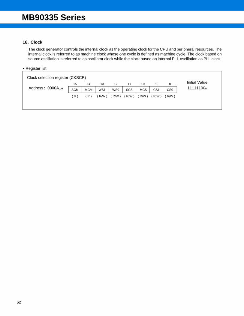
MB90335 Series
62
18. Clock
The clock generator controls the internal clock as the operating clock for the CPU and peripheral resources. Theinternal clock is referred to as machine clock whose one cycle is defined as machine cycle. The clock based onsource oscillation is referred to as oscillator clock while the clock based on internal PLL oscillation as PLL clock.
• Register list
Clock selection register (CKSCR) Initial Value
Address : 0000A1H 11111100B
( R ) ( R/W ) ( R/W ) ( R/W ) ( R/W ) ( R/W ) ( R/W )
15 14 13 12 11 10 9 8
MCM
( R )
SCM WS1 WS0 SCS MCS CS1 CS0
MB90335 Series
19. 512 Kbits flash memory
The description that follows applies to the flash memory built in the MB90F337; it is not applicable to evaluationROM or masked ROM.
The method of data write/erase to flash memory is following three types. • Parallel writer• Serial dedicated writer• Write/erase by executing program
• Description of 512 Kbits flash memory
512 Kbits flash memory is located in FFH bank in the CPU memory map. Function of flash memory interfacecircuit enables read and program access from CPU. Write/erase to flash interface is executed by instruction from CPU via flash memory interface, so rewrite ofprogram and data is carried on in the mounting state effectively.
Data can be reprogrammed not only by program execution in existing RAM but by program execution in flashmemory by dual operation. Also, erase/write and read in the defferent bank (Upper Bank/Lower Bank) is executedsimultaneously.
• Features of 512 Kbits flash memory• Sector configuration : 64 Kwords × 8 bits/32 words × 16 bits (4K × 4 + 16K × 2 + 4K × 4) • Simultaneous execution of erase/write and read by 2-bank configuration• Automatic program algorithm (Embeded AlgorithmTM*) • Built-in deletion pause/deletion resume function• Detection of programming/erasure completion using data polling and the toggle bit • At least 10,000 times guaranteed• Minimum flash read cycle time : 2 machine cycles
* : Embedded AlgorithmTM is a trade mark of Advanced Micro Devices Inc.
Note : The read function of manufacture code and device coad is not including. Also, these code is not accessed by the command.
• Flash write/erase• Flash memory can not execute write/erase and read by the same bank simultaneously. • Data can be programmed/deleted into and erased from flash memory by executing either the program
residing in the flash memory or the one copied to RAM from the flash memory.
63
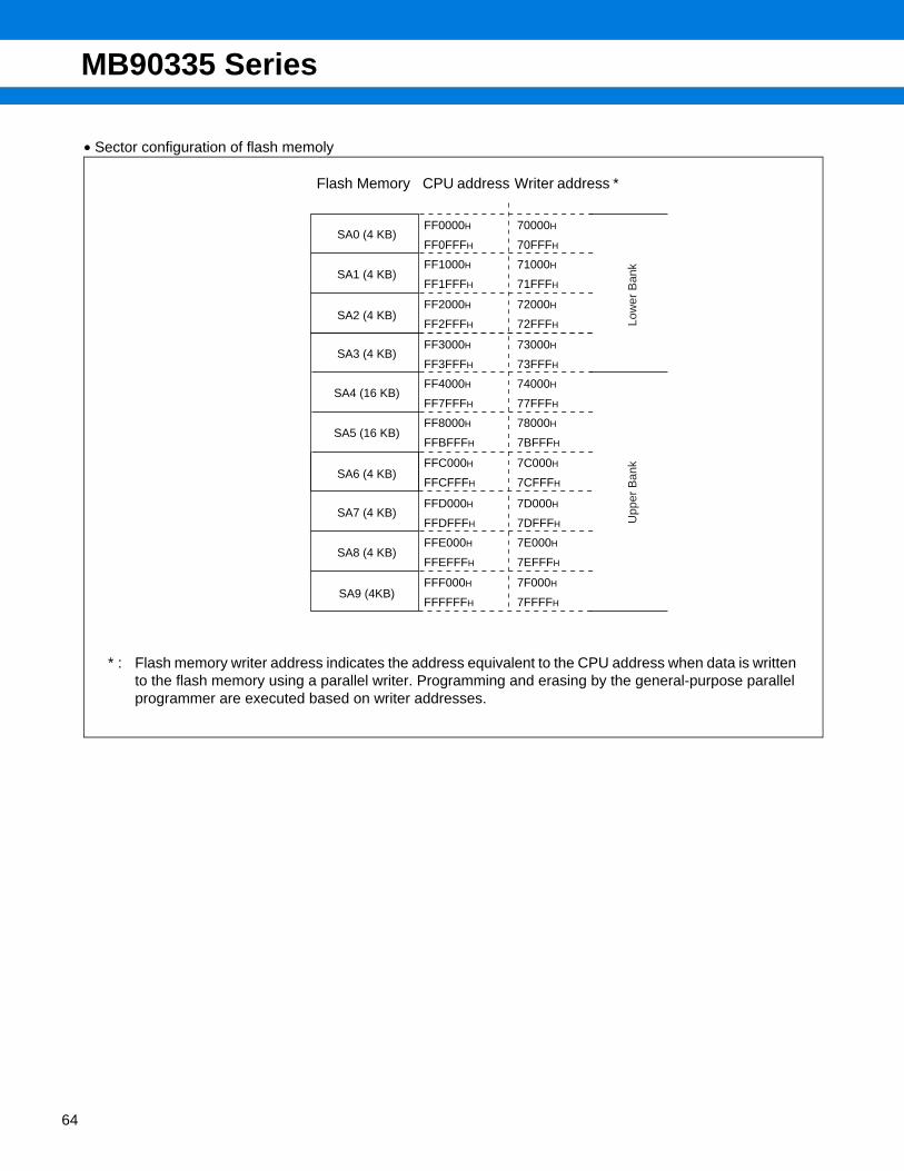
MB90335 Series
64
• Sector configuration of flash memoly
SA0 (4 KB)
SA1 (4 KB)
SA2 (4 KB)
SA3 (4 KB)
FF0000H
FF0FFFH
FF1000H
FF1FFFH
FF2000H
FF2FFFH
70000H
70FFFH
71000H
71FFFH
72000H
72FFFH
SA4 (16 KB)
SA5 (16 KB)
SA6 (4 KB)
FF3000H
FF3FFFH
FF4000H
FF7FFFH
FF8000H
FFBFFFH
FFC000H
FFCFFFH
73000H
73FFFH
74000H
77FFFH
78000H
7BFFFH
7C000H
7CFFFH
SA7 (4 KB)
SA8 (4 KB)
SA9 (4KB)
FFD000H
FFDFFFH
FFE000H
FFEFFFH
FFF000H
FFFFFFH
7D000H
7DFFFH
7E000H
7EFFFH
7F000H
7FFFFH
Low
er B
ank
Upp
er B
ank
Flash Memory CPU address Writer address *
* : Flash memory writer address indicates the address equivalent to the CPU address when data is written to the flash memory using a parallel writer. Programming and erasing by the general-purpose parallel programmer are executed based on writer addresses.
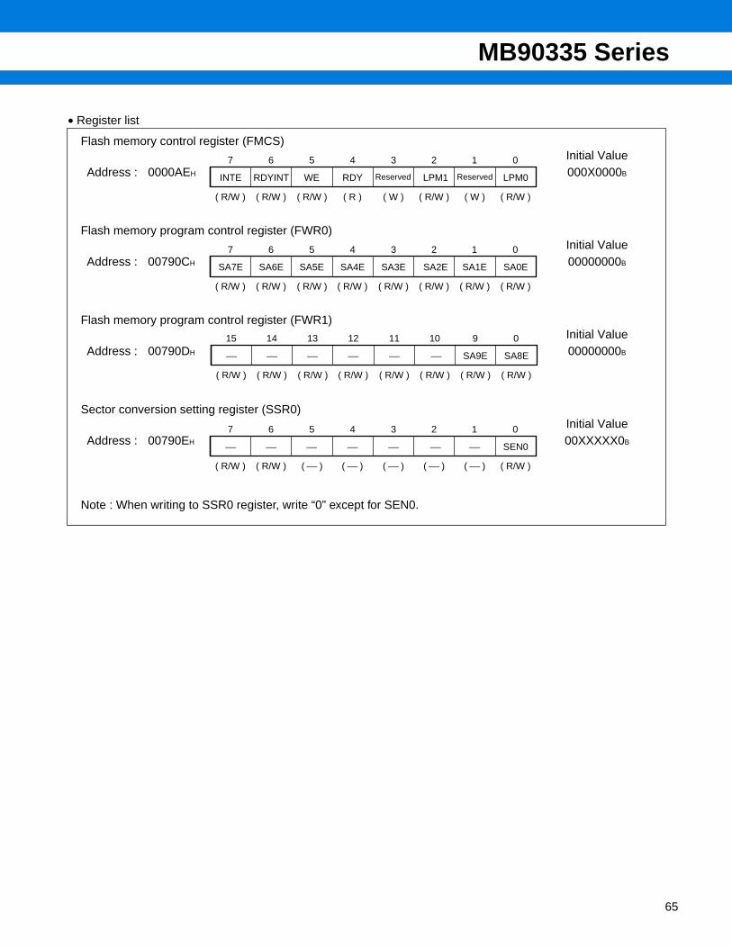
MB90335 Series
• Register list
Flash memory control register (FMCS)
Flash memory program control register (FWR0)
Flash memory program control register (FWR1)
Sector conversion setting register (SSR0)
Note : When writing to SSR0 register, write “0” except for SEN0.
Initial ValueAddress : 0000AEH 000X0000B
Initial ValueAddress : 00790CH 00000000B
Initial ValueAddress : 00790DH 00000000B
Initial ValueAddress : 00790EH 00XXXXX0B
( R/W ) ( R/W ) ( R ) ( W ) ( R/W ) ( W ) ( R/W )
7 6 5 4 3 2 1 0
RDYINT
( R/W )
INTE WE RDY LPM1 LPM0Reserved Reserved
( R/W ) ( R/W ) ( R/W ) ( R/W ) ( R/W ) ( R/W ) ( R/W )
7 6 5 4 3 2 1 0
SA6E
( R/W )
SA7E SA5E SA4E SA3E SA2E SA1E SA0E
( R/W ) ( R/W ) ( R/W ) ( R/W ) ( R/W ) ( R/W ) ( R/W )
15 14 13 12 11 10 9 0
⎯
( R/W )
⎯ ⎯ ⎯ ⎯ ⎯ SA9E SA8E
( R/W ) ( ⎯ ) ( ⎯ ) ( ⎯ ) ( ⎯ ) ( ⎯ ) ( R/W )
7 6 5 4 3 2 1 0
⎯
( R/W )
⎯ ⎯ ⎯ ⎯ ⎯ ⎯ SEN0
65
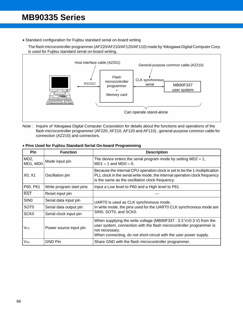
MB90335 Series
66
• Standard configuration for Fujitsu standard serial on-board writing
The flash microcontroller programmer (AF220/AF210/AF120/AF110) made by Yokogawa Digital Computer Corp.is used for Fujitsu standard serial on-board writing.
Note : Inquire of Yokogawa Digital Computer Corporation for details about the functions and operations of the flash microcontroller programmer (AF220, AF210, AF120 and AF110) , general-purpose common cable for connection (AZ210) and connectors.
• Pins Used for Fujitsu Standard Serial On-board Programming
Pin Function Description
MD2, MD1, MD0
Mode input pinThe device enters the serial program mode by setting MD2 = 1, MD1 = 1 and MD0 = 0.
X0, X1 Oscillation pinBecause the internal CPU operation clock is set to be the 1 multiplication PLL clock in the serial write mode, the internal operation clock frequency is the same as the oscillation clock frequency.
P60, P61 Write program start pins Input a Low level to P60 and a High level to P61.
RST Reset input pin ⎯
SIN0 Serial data input pin UART0 is used as CLK synchronous mode.In write mode, the pins used for the UART0 CLK synchronous mode are SIN0, SOT0, and SCK0.
SOT0 Serial data output pin
SCK0 Serial clock input pin
VCC Power source input pin
When supplying the write voltage (MB90F337 : 3.3 V±0.3 V) from the user system, connection with the flash microcontroller programmer is not necessary.When connecting, do not short-circuit with the user power supply.
VSS GND Pin Share GND with the flash microcontroller programmer.
RS232C
Host interface cable (AZ201) General-purpose common cable (AZ210)
CLK synchronous serial MB90F337
user system
Can operate stand-alone
Flash microcontroller
programmer+
Memory card
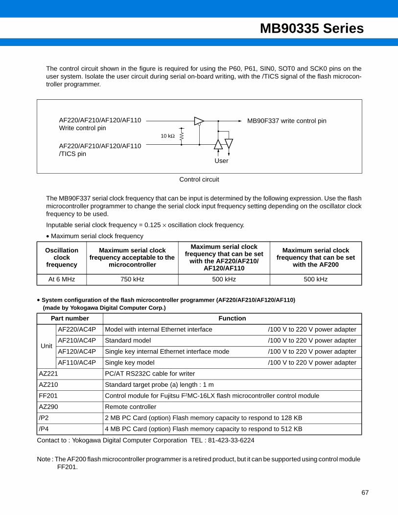
MB90335 Series
The control circuit shown in the figure is required for using the P60, P61, SIN0, SOT0 and SCK0 pins on theuser system. Isolate the user circuit during serial on-board writing, with the /TICS signal of the flash microcon-troller programmer.
Control circuit
The MB90F337 serial clock frequency that can be input is determined by the following expression. Use the flashmicrocontroller programmer to change the serial clock input frequency setting depending on the oscillator clockfrequency to be used.
Inputable serial clock frequency = 0.125 × oscillation clock frequency.
• Maximum serial clock frequency
• System configuration of the flash microcontroller programmer (AF220/AF210/AF120/AF110) (made by Yokogawa Digital Computer Corp.)
Contact to : Yokogawa Digital Computer Corporation TEL : 81-423-33-6224
Note : The AF200 flash microcontroller programmer is a retired product, but it can be supported using control module FF201.
Oscillation clock
frequency
Maximum serial clock frequency acceptable to the
microcontroller
Maximum serial clock frequency that can be set
with the AF220/AF210/AF120/AF110
Maximum serial clock frequency that can be set
with the AF200
At 6 MHz 750 kHz 500 kHz 500 kHz
Part number Function
Unit
AF220/AC4P Model with internal Ethernet interface /100 V to 220 V power adapter
AF210/AC4P Standard model /100 V to 220 V power adapter
AF120/AC4P Single key internal Ethernet interface mode /100 V to 220 V power adapter
AF110/AC4P Single key model /100 V to 220 V power adapter
AZ221 PC/AT RS232C cable for writer
AZ210 Standard target probe (a) length : 1 m
FF201 Control module for Fujitsu F2MC-16LX flash microcontroller control module
AZ290 Remote controller
/P2 2 MB PC Card (option) Flash memory capacity to respond to 128 KB
/P4 4 MB PC Card (option) Flash memory capacity to respond to 512 KB
10 kΩ
AF220/AF210/AF120/AF110Write control pin
AF220/AF210/AF120/AF110/TICS pin
MB90F337 write control pin
User
67
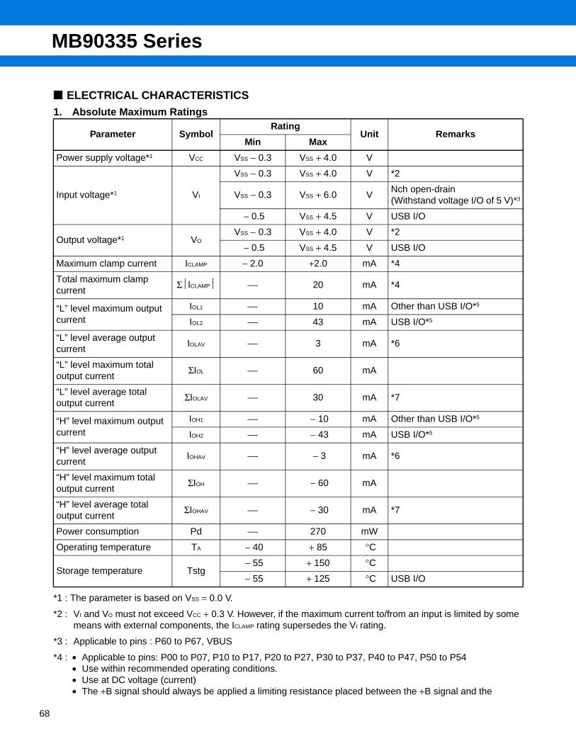
MB90335 Series
68
ELECTRICAL CHARACTERISTICS1. Absolute Maximum Ratings
*1 : The parameter is based on VSS = 0.0 V.
*2 : VI and VO must not exceed VCC + 0.3 V. However, if the maximum current to/from an input is limited by some means with external components, the ICLAMP rating supersedes the VI rating.
*3 : Applicable to pins : P60 to P67, VBUS
*4 : • Applicable to pins: P00 to P07, P10 to P17, P20 to P27, P30 to P37, P40 to P47, P50 to P54• Use within recommended operating conditions.• Use at DC voltage (current) • The +B signal should always be applied a limiting resistance placed between the +B signal and the
Parameter SymbolRating
Unit RemarksMin Max
Power supply voltage*1 VCC VSS − 0.3 VSS + 4.0 V
Input voltage*1 VI
VSS − 0.3 VSS + 4.0 V *2
VSS − 0.3 VSS + 6.0 VNch open-drain(Withstand voltage I/O of 5 V)*3
− 0.5 VSS + 4.5 V USB I/O
Output voltage*1 VOVSS − 0.3 VSS + 4.0 V *2
− 0.5 VSS + 4.5 V USB I/O
Maximum clamp current ICLAMP − 2.0 +2.0 mA *4
Total maximum clamp current
ΣICLAMP ⎯ 20 mA *4
“L” level maximum output current
IOL1 ⎯ 10 mA Other than USB I/O*5
IOL2 ⎯ 43 mA USB I/O*5
“L” level average output current
IOLAV ⎯ 3 mA *6
“L” level maximum total output current
ΣIOL ⎯ 60 mA
“L” level average total output current
ΣIOLAV ⎯ 30 mA *7
“H” level maximum output current
IOH1 ⎯ − 10 mA Other than USB I/O*5
IOH2 ⎯ − 43 mA USB I/O*5
“H” level average output current
IOHAV ⎯ − 3 mA *6
“H” level maximum total output current
ΣIOH ⎯ − 60 mA
“H” level average total output current
ΣIOHAV ⎯ − 30 mA *7
Power consumption Pd ⎯ 270 mW
Operating temperature TA − 40 + 85 °C
Storage temperature Tstg − 55 + 150 °C
− 55 + 125 °C USB I/O
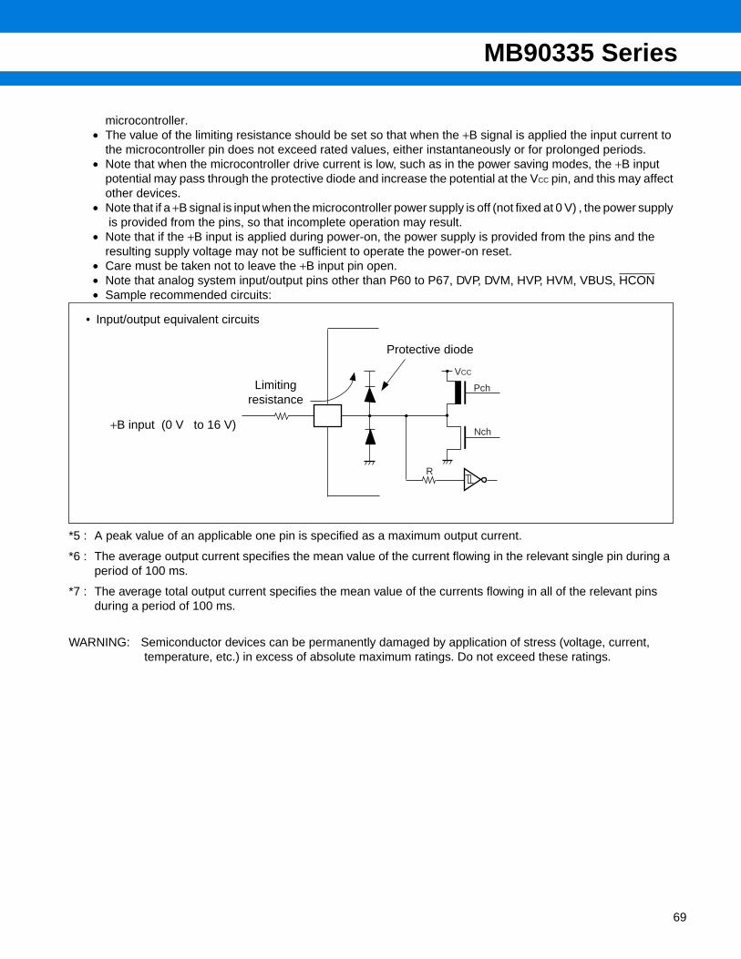
MB90335 Series
microcontroller.• The value of the limiting resistance should be set so that when the +B signal is applied the input current to
the microcontroller pin does not exceed rated values, either instantaneously or for prolonged periods.• Note that when the microcontroller drive current is low, such as in the power saving modes, the +B input
potential may pass through the protective diode and increase the potential at the VCC pin, and this may affectother devices.
• Note that if a +B signal is input when the microcontroller power supply is off (not fixed at 0 V) , the power supply is provided from the pins, so that incomplete operation may result.
• Note that if the +B input is applied during power-on, the power supply is provided from the pins and the resulting supply voltage may not be sufficient to operate the power-on reset.
• Care must be taken not to leave the +B input pin open.• Note that analog system input/output pins other than P60 to P67, DVP, DVM, HVP, HVM, VBUS, HCON• Sample recommended circuits:
*5 : A peak value of an applicable one pin is specified as a maximum output current.
*6 : The average output current specifies the mean value of the current flowing in the relevant single pin during a period of 100 ms.
*7 : The average total output current specifies the mean value of the currents flowing in all of the relevant pins during a period of 100 ms.
WARNING: Semiconductor devices can be permanently damaged by application of stress (voltage, current, temperature, etc.) in excess of absolute maximum ratings. Do not exceed these ratings.
Pch
Nch
VCC
R
• Input/output equivalent circuits
+B input (0 V to 16 V)
Limitingresistance
Protective diode
69
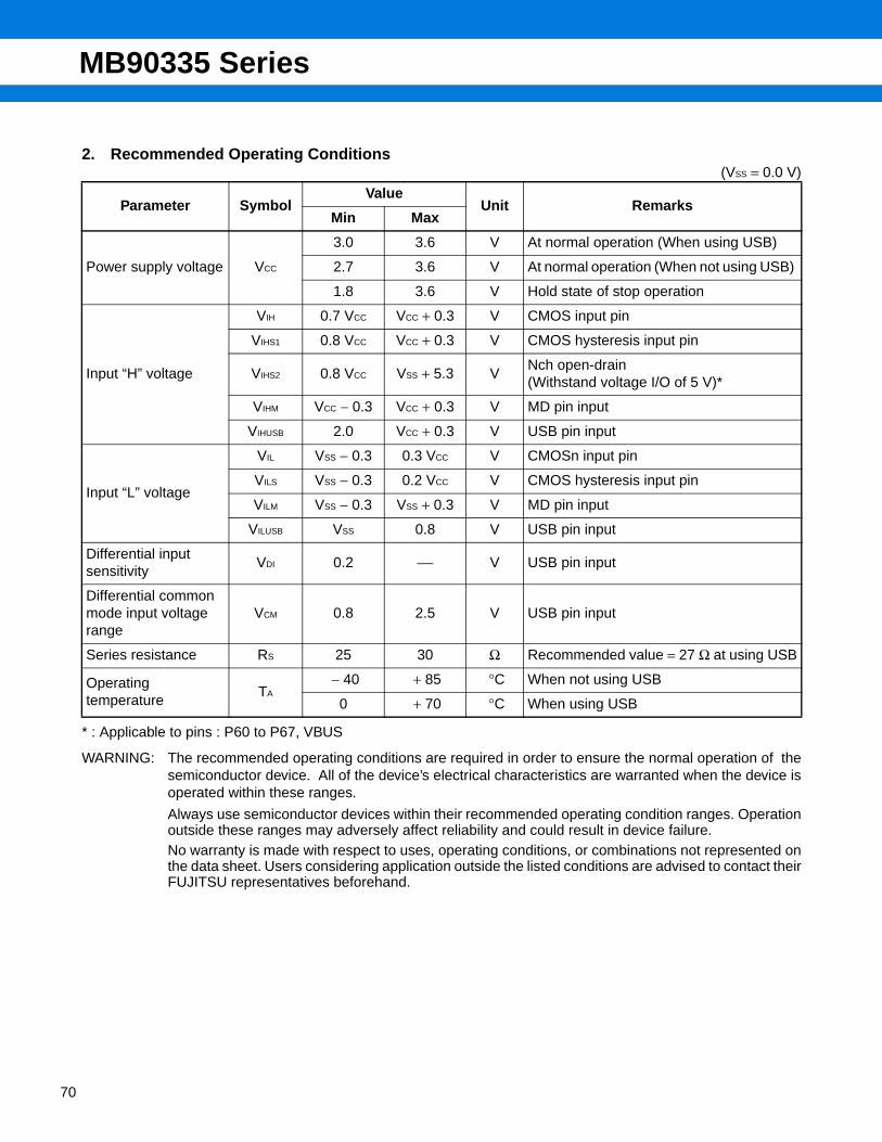
MB90335 Series
70
2. Recommended Operating Conditions(VSS = 0.0 V)
* : Applicable to pins : P60 to P67, VBUS
WARNING: The recommended operating conditions are required in order to ensure the normal operation of thesemiconductor device. All of the device’s electrical characteristics are warranted when the device isoperated within these ranges.
Always use semiconductor devices within their recommended operating condition ranges. Operationoutside these ranges may adversely affect reliability and could result in device failure.No warranty is made with respect to uses, operating conditions, or combinations not represented onthe data sheet. Users considering application outside the listed conditions are advised to contact theirFUJITSU representatives beforehand.
Parameter SymbolValue
Unit RemarksMin Max
Power supply voltage VCC
3.0 3.6 V At normal operation (When using USB)
2.7 3.6 V At normal operation (When not using USB)
1.8 3.6 V Hold state of stop operation
Input “H” voltage
VIH 0.7 VCC VCC + 0.3 V CMOS input pin
VIHS1 0.8 VCC VCC + 0.3 V CMOS hysteresis input pin
VIHS2 0.8 VCC VSS + 5.3 VNch open-drain(Withstand voltage I/O of 5 V)*
VIHM VCC − 0.3 VCC + 0.3 V MD pin input
VIHUSB 2.0 VCC + 0.3 V USB pin input
Input “L” voltage
VIL VSS − 0.3 0.3 VCC V CMOSn input pin
VILS VSS − 0.3 0.2 VCC V CMOS hysteresis input pin
VILM VSS − 0.3 VSS + 0.3 V MD pin input
VILUSB VSS 0.8 V USB pin input
Differential input sensitivity
VDI 0.2 ⎯ V USB pin input
Differential common mode input voltage range
VCM 0.8 2.5 V USB pin input
Series resistance RS 25 30 Ω Recommended value = 27 Ω at using USB
Operating temperature
TA − 40 + 85 °C When not using USB
0 + 70 °C When using USB
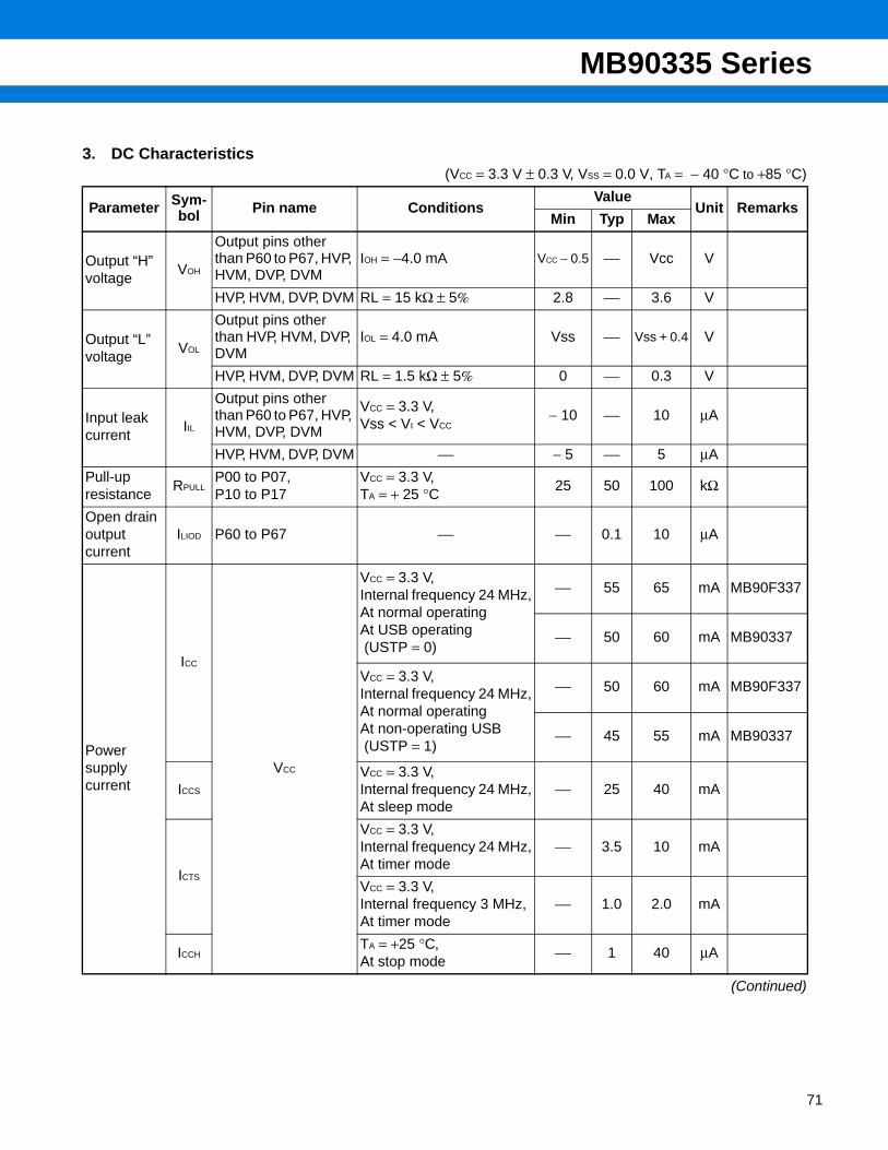
MB90335 Series
3. DC Characteristics (VCC = 3.3 V ± 0.3 V, VSS = 0.0 V, TA = − 40 °C to +85 °C)
(Continued)
Parameter Sym-bol Pin name Conditions
ValueUnit Remarks
Min Typ Max
Output “H” voltage
VOH
Output pins other than P60 to P67, HVP, HVM, DVP, DVM
IOH = −4.0 mA VCC − 0.5 ⎯ Vcc V
HVP, HVM, DVP, DVM RL = 15 kΩ ± 5% 2.8 ⎯ 3.6 V
Output “L” voltage
VOL
Output pins other than HVP, HVM, DVP, DVM
IOL = 4.0 mA Vss ⎯ Vss + 0.4 V
HVP, HVM, DVP, DVM RL = 1.5 kΩ ± 5% 0 ⎯ 0.3 V
Input leak current
IIL
Output pins other than P60 to P67, HVP, HVM, DVP, DVM
VCC = 3.3 V, Vss < VI < VCC
− 10 ⎯ 10 µA
HVP, HVM, DVP, DVM ⎯ − 5 ⎯ 5 µA
Pull-up resistance
RPULLP00 to P07, P10 to P17
VCC = 3.3 V, TA = + 25 °C 25 50 100 kΩ
Open drain output current
ILIOD P60 to P67 ⎯ ⎯ 0.1 10 µA
Power supply current
ICC
VCC
VCC = 3.3 V, Internal frequency 24 MHz,At normal operatingAt USB operating (USTP = 0)
⎯ 55 65 mA MB90F337
⎯ 50 60 mA MB90337
VCC = 3.3 V, Internal frequency 24 MHz,At normal operatingAt non-operating USB (USTP = 1)
⎯ 50 60 mA MB90F337
⎯ 45 55 mA MB90337
ICCS
VCC = 3.3 V, Internal frequency 24 MHz,At sleep mode
⎯ 25 40 mA
ICTS
VCC = 3.3 V, Internal frequency 24 MHz,At timer mode
⎯ 3.5 10 mA
VCC = 3.3 V, Internal frequency 3 MHz,At timer mode
⎯ 1.0 2.0 mA
ICCHTA = +25 °C, At stop mode
⎯ 1 40 µA
71
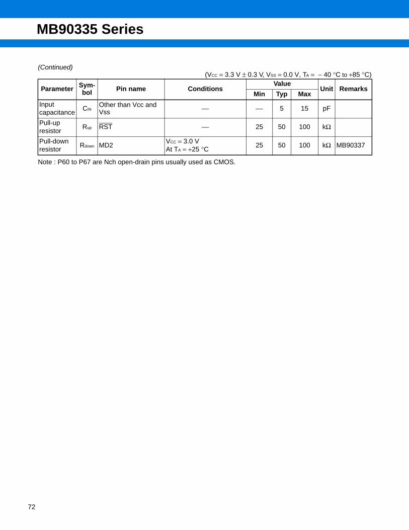
MB90335 Series
72
(Continued)(VCC = 3.3 V ± 0.3 V, VSS = 0.0 V, TA = − 40 °C to +85 °C)
Note : P60 to P67 are Nch open-drain pins usually used as CMOS.
Parameter Sym-bol Pin name Conditions
ValueUnit Remarks
Min Typ Max
Input capacitance
CINOther than Vcc and Vss ⎯ ⎯ 5 15 pF
Pull-up resistor
Rup RST ⎯ 25 50 100 kΩ
Pull-down resistor
Rdown MD2VCC = 3.0 VAt TA = +25 °C 25 50 100 kΩ MB90337
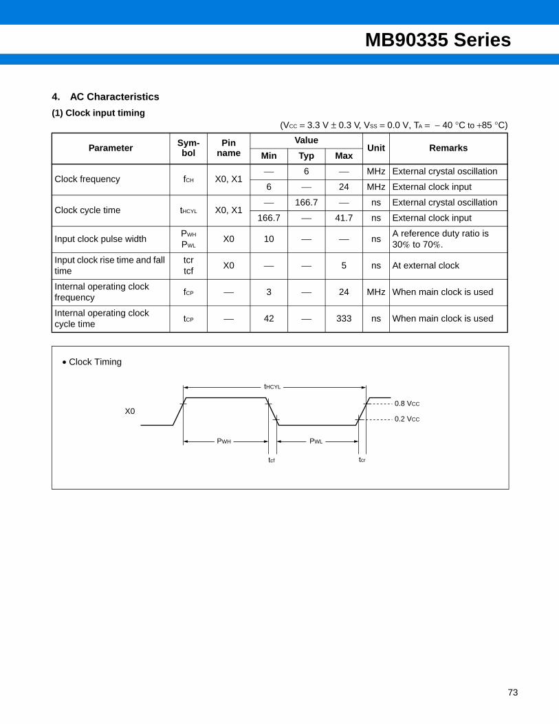
MB90335 Series
4. AC Characteristics
(1) Clock input timing (VCC = 3.3 V ± 0.3 V, VSS = 0.0 V, TA = − 40 °C to +85 °C)
Parameter Sym-bol
Pin name
ValueUnit Remarks
Min Typ Max
Clock frequency fCH X0, X1⎯ 6 ⎯ MHz External crystal oscillation
6 ⎯ 24 MHz External clock input
Clock cycle time tHCYL X0, X1⎯ 166.7 ⎯ ns External crystal oscillation
166.7 ⎯ 41.7 ns External clock input
Input clock pulse widthPWH
PWLX0 10 ⎯ ⎯ ns
A reference duty ratio is 30% to 70%.
Input clock rise time and fall time
tcrtcf
X0 ⎯ ⎯ 5 ns At external clock
Internal operating clock frequency
fCP ⎯ 3 ⎯ 24 MHz When main clock is used
Internal operating clock cycle time
tCP ⎯ 42 ⎯ 333 ns When main clock is used
0.8 VCC
0.2 VCC
tcf tcr
tHCYL
PWH PWL
X0
• Clock Timing
73
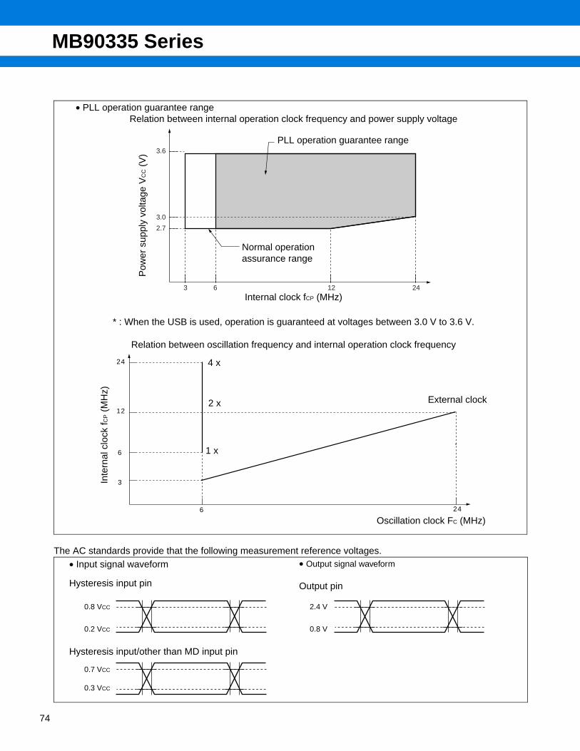
MB90335 Series
74
The AC standards provide that the following measurement reference voltages.
• PLL operation guarantee rangeRelation between internal operation clock frequency and power supply voltage
* : When the USB is used, operation is guaranteed at voltages between 3.0 V to 3.6 V.
Relation between oscillation frequency and internal operation clock frequency
3.6
3.0
2.7
3 6 12 24
Internal clock fCP (MHz)
Pow
er s
uppl
y vo
ltage
VC
C (
V)
PLL operation guarantee range
Normal operation assurance range
3
12
6
6
24
24
Inte
rnal
clo
ck f C
P (
MH
z)
Oscillation clock FC (MHz)
4 x
2 x
1 x
External clock
0.8 VCC
0.2 VCC
2.4 V
0.8 V
0.7 VCC
0.3 VCC
• Input signal waveform
Hysteresis input pin
Hysteresis input/other than MD input pin
• Output signal waveform
Output pin
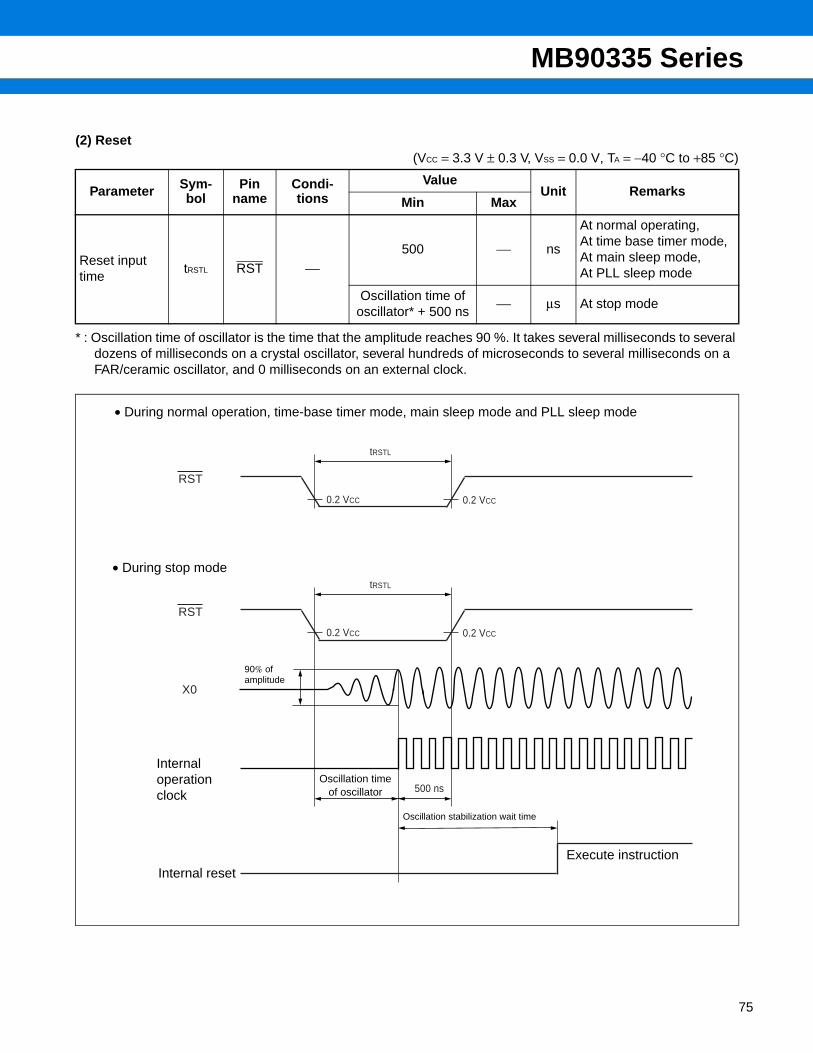
MB90335 Series
(2) Reset (VCC = 3.3 V ± 0.3 V, VSS = 0.0 V, TA = −40 °C to +85 °C)
* : Oscillation time of oscillator is the time that the amplitude reaches 90 %. It takes several milliseconds to several dozens of milliseconds on a crystal oscillator, several hundreds of microseconds to several milliseconds on a FAR/ceramic oscillator, and 0 milliseconds on an external clock.
Parameter Sym-bol
Pin name
Condi-tions
ValueUnit Remarks
Min Max
Reset input time
tRSTL RST ⎯500 ⎯ ns
At normal operating, At time base timer mode, At main sleep mode, At PLL sleep mode
Oscillation time of oscillator* + 500 ns
⎯ µs At stop mode
RST
X0
500 ns
tRSTL
0.2 VCC 0.2 VCC
RST
tRSTL
0.2 VCC 0.2 VCC
• During stop mode
Internal operation clock
Internal reset
Oscillation time of oscillator
Oscillation stabilization wait time
Execute instruction
90% of amplitude
• During normal operation, time-base timer mode, main sleep mode and PLL sleep mode
75
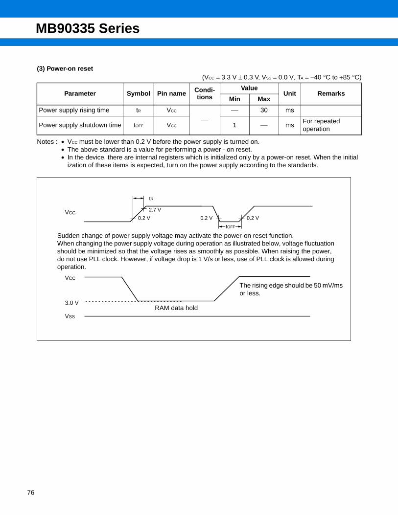
MB90335 Series
76
(3) Power-on reset (VCC = 3.3 V ± 0.3 V, VSS = 0.0 V, TA = −40 °C to +85 °C)
Notes : • VCC must be lower than 0.2 V before the power supply is turned on. • The above standard is a value for performing a power - on reset. • In the device, there are internal registers which is initialized only by a power-on reset. When the initial
ization of these items is expected, turn on the power supply according to the standards.
Parameter Symbol Pin name Condi-tions
ValueUnit Remarks
Min Max
Power supply rising time tR VCC
⎯⎯ 30 ms
Power supply shutdown time tOFF VCC 1 ⎯ msFor repeated operation
VCC
VCC
3.0 V
VSS
tR
0.2 V0.2 V
2.7 V
tOFF
0.2 V
Sudden change of power supply voltage may activate the power-on reset function.When changing the power supply voltage during operation as illustrated below, voltage fluctuation should be minimized so that the voltage rises as smoothly as possible. When raising the power, do not use PLL clock. However, if voltage drop is 1 V/s or less, use of PLL clock is allowed during operation.
RAM data hold
The rising edge should be 50 mV/ms or less.
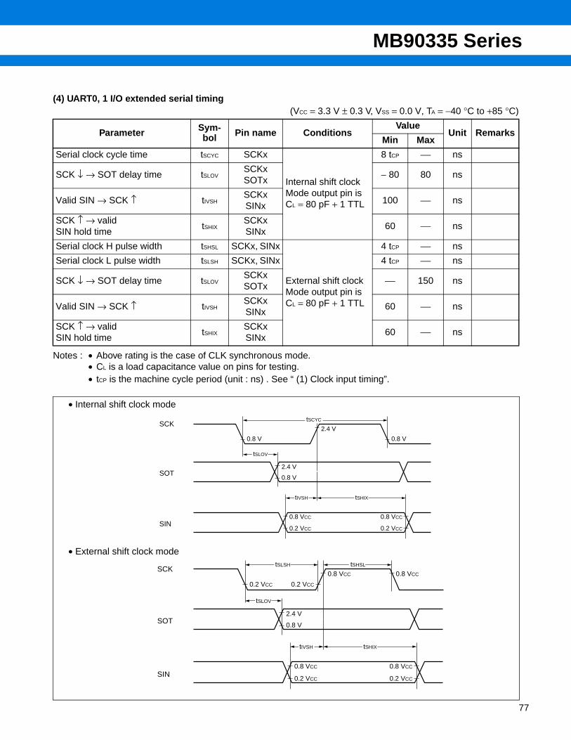
MB90335 Series
(4) UART0, 1 I/O extended serial timing (VCC = 3.3 V ± 0.3 V, VSS = 0.0 V, TA = −40 °C to +85 °C)
Notes : • Above rating is the case of CLK synchronous mode.• CL is a load capacitance value on pins for testing.• tCP is the machine cycle period (unit : ns) . See “ (1) Clock input timing”.
Parameter Sym-bol Pin name Conditions
ValueUnit Remarks
Min Max
Serial clock cycle time tSCYC SCKx
Internal shift clock Mode output pin isCL = 80 pF + 1 TTL
8 tCP ⎯ ns
SCK ↓ → SOT delay time tSLOVSCKxSOTx
− 80 80 ns
Valid SIN → SCK ↑ tIVSHSCKxSINx
100 ⎯ ns
SCK ↑ → valid SIN hold time
tSHIXSCKxSINx
60 ⎯ ns
Serial clock H pulse width tSHSL SCKx, SINx
External shift clock Mode output pin isCL = 80 pF + 1 TTL
4 tCP ⎯ ns
Serial clock L pulse width tSLSH SCKx, SINx 4 tCP ⎯ ns
SCK ↓ → SOT delay time tSLOVSCKxSOTx
⎯ 150 ns
Valid SIN → SCK ↑ tIVSHSCKxSINx
60 ⎯ ns
SCK ↑ → valid SIN hold time
tSHIXSCKxSINx
60 ⎯ ns
• Internal shift clock mode
• External shift clock mode
SCK
SOT
SIN
tSCYC
tSLOV
tIVSH tSHIX
0.8 V 0.8 V
2.4 V
2.4 V
0.8 V
0.8 VCC
0.2 VCC
0.8 VCC
0.2 VCC
SCK
SOT
SIN
tSLSH tSHSL
tSLOV
tIVSH tSHIX
0.2 VCC 0.2 VCC
0.8 VCC 0.8 VCC
2.4 V
0.8 V
0.8 VCC
0.2 VCC
0.8 VCC
0.2 VCC
77
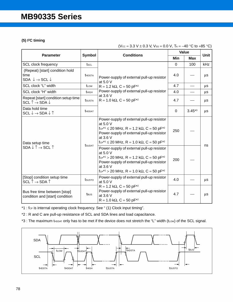
MB90335 Series
78
(5) I2C timing
(VCC = 3.3 V ± 0.3 V, VSS = 0.0 V, TA = −40 °C to +85 °C)
*1 : fCP is internal operating clock frequency. See “ (1) Clock input timing”.
*2 : R and C are pull-up resistance of SCL and SDA lines and load capacitance.
*3 : The maximum tHDDAT only has to be met if the device does not stretch the “L” width (tLOW) of the SCL signal.
Parameter Symbol ConditionsValue
UnitMin Max
SCL clock frequency tSCL
Power-supply of external pull-up resistor at 5.0 VR = 1.2 kΩ, C = 50 pF*2
Power-supply of external pull-up resistor at 3.6 VR = 1.0 kΩ, C = 50 pF*2
0 100 kHz
(Repeat) [start] condition hold timeSDA ↓ → SCL ↓
tHDSTA 4.0 ⎯ µs
SCL clock “L” width tLOW 4.7 ⎯ µs
SCL clock “H” width tHIGH 4.0 ⎯ µs
Repeat [start] condition setup timeSCL ↑ → SDA ↓ tSUSTA 4.7 ⎯ µs
Data hold timeSCL ↓ → SDA ↓ ↑ tHDDAT 0 3.45*3 µs
Data setup timeSDA ↓ ↑ → SCL ↑ tSUDAT
Power-supply of external pull-up resistor at 5.0 VfCP*1 ≤ 20 MHz, R = 1.2 kΩ, C = 50 pF*2
Power-supply of external pull-up resistor at 3.6 VfCP*1 ≤ 20 MHz, R = 1.0 kΩ, C = 50 pF*2
250 ⎯
nsPower-supply of external pull-up resistor at 5.0 VfCP*1 > 20 MHz, R = 1.2 kΩ, C = 50 pF*2
Power-supply of external pull-up resistor at 3.6 VfCP*1 > 20 MHz, R = 1.0 kΩ, C = 50 pF*2
200 ⎯
[Stop] condition setup timeSCL ↑ → SDA ↑ tSUSTO
Power-supply of external pull-up resistor at 5.0 VR = 1.2 kΩ, C = 50 pF*2
Power-supply of external pull-up resistor at 3.6 VR = 1.0 kΩ, C = 50 pF*2
4.0 ⎯ µs
Bus free time between [stop] condition and [start] condition
tBUS 4.7 ⎯ µs
SDA
SCL
tLOW
tHDSTA tHDDAT
tSUDAT
tSUSTA tSUSTO
tHDSTA
tHIGH
tBUS
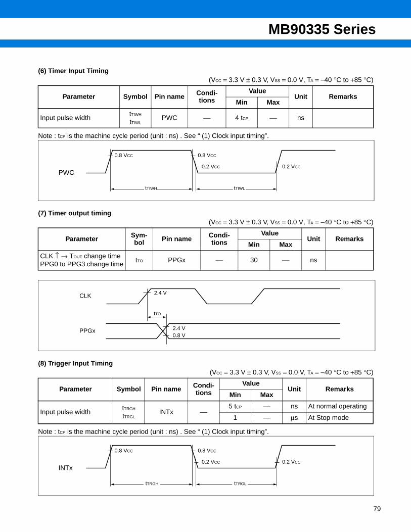
MB90335 Series
(6) Timer Input Timing (VCC = 3.3 V ± 0.3 V, VSS = 0.0 V, TA = −40 °C to +85 °C)
Note : tCP is the machine cycle period (unit : ns) . See “ (1) Clock input timing”.
(7) Timer output timing (VCC = 3.3 V ± 0.3 V, VSS = 0.0 V, TA = −40 °C to +85 °C)
(8) Trigger Input Timing (VCC = 3.3 V ± 0.3 V, VSS = 0.0 V, TA = −40 °C to +85 °C)
Note : tCP is the machine cycle period (unit : ns) . See “ (1) Clock input timing”.
Parameter Symbol Pin name Condi-tions
ValueUnit Remarks
Min Max
Input pulse widthtTIWH
tTIWLPWC ⎯ 4 tCP ⎯ ns
Parameter Sym-bol Pin name Condi-
tionsValue
Unit RemarksMin Max
CLK ↑ → TOUT change timePPG0 to PPG3 change time
tTO PPGx ⎯ 30 ⎯ ns
Parameter Symbol Pin name Condi-tions
ValueUnit Remarks
Min Max
Input pulse widthtTRGH
tTRGLINTx ⎯
5 tCP ⎯ ns At normal operating
1 ⎯ µs At Stop mode
0.8 VCC 0.8 VCC
0.2 VCC 0.2 VCC
tTIWH tTIWL
PWC
CLK
PPGx
2.4 V
tTO
2.4 V0.8 V
0.8 VCC 0.8 VCC
0.2 VCC 0.2 VCC
tTRGH tTRGL
INTx
79
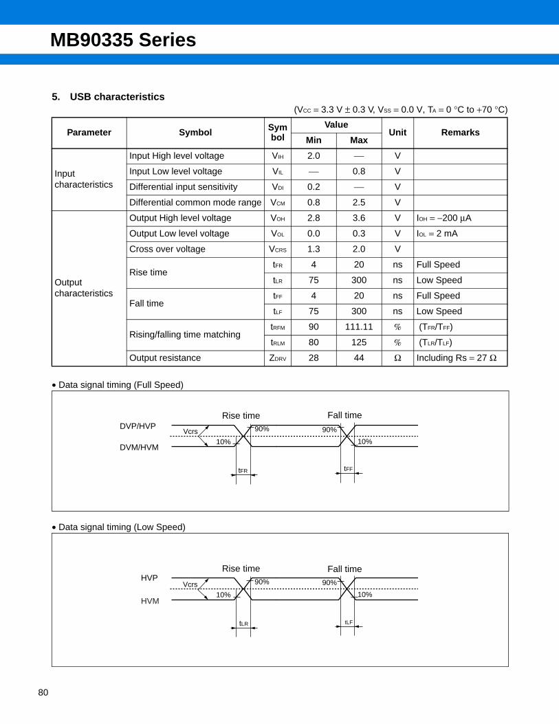
MB90335 Series
80
5. USB characteristics (VCC = 3.3 V ± 0.3 V, VSS = 0.0 V, TA = 0 °C to +70 °C)
• Data signal timing (Full Speed)
• Data signal timing (Low Speed)
Parameter Symbol Symbol
ValueUnit Remarks
Min Max
Input characteristics
Input High level voltage VIH 2.0 ⎯ V
Input Low level voltage VIL ⎯ 0.8 V
Differential input sensitivity VDI 0.2 ⎯ V
Differential common mode range VCM 0.8 2.5 V
Outputcharacteristics
Output High level voltage VOH 2.8 3.6 V IOH = −200 µA
Output Low level voltage VOL 0.0 0.3 V IOL = 2 mA
Cross over voltage VCRS 1.3 2.0 V
Rise timetFR 4 20 ns Full Speed
tLR 75 300 ns Low Speed
Fall timetFF 4 20 ns Full Speed
tLF 75 300 ns Low Speed
Rising/falling time matchingtRFM 90 111.11 % (TFR/TFF)
tRLM 80 125 % (TLR/TLF)
Output resistance ZDRV 28 44 Ω Including Rs = 27 Ω
DVM/HVM
90%
tFR
10%
90%
10%
tFF
VcrsDVP/HVP
Rise time Fall time
HVP 90%
tLR
10%
90%
10%
tLF
Vcrs
HVM
Rise time Fall time
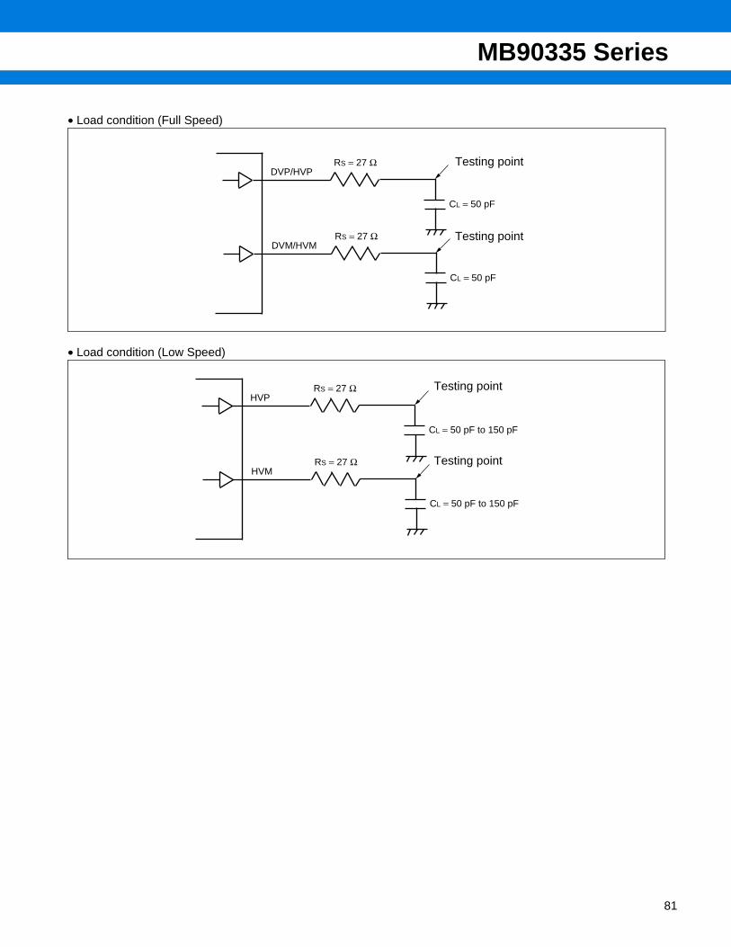
MB90335 Series
• Load condition (Full Speed)
• Load condition (Low Speed)
DVP/HVPRS = 27 Ω
CL = 50 pF
DVM/HVMRS = 27 Ω
CL = 50 pF
Testing point
Testing point
HVPRS = 27 Ω
CL = 50 pF to 150 pF
HVMRS = 27 Ω
CL = 50 pF to 150 pF
Testing point
Testing point
81
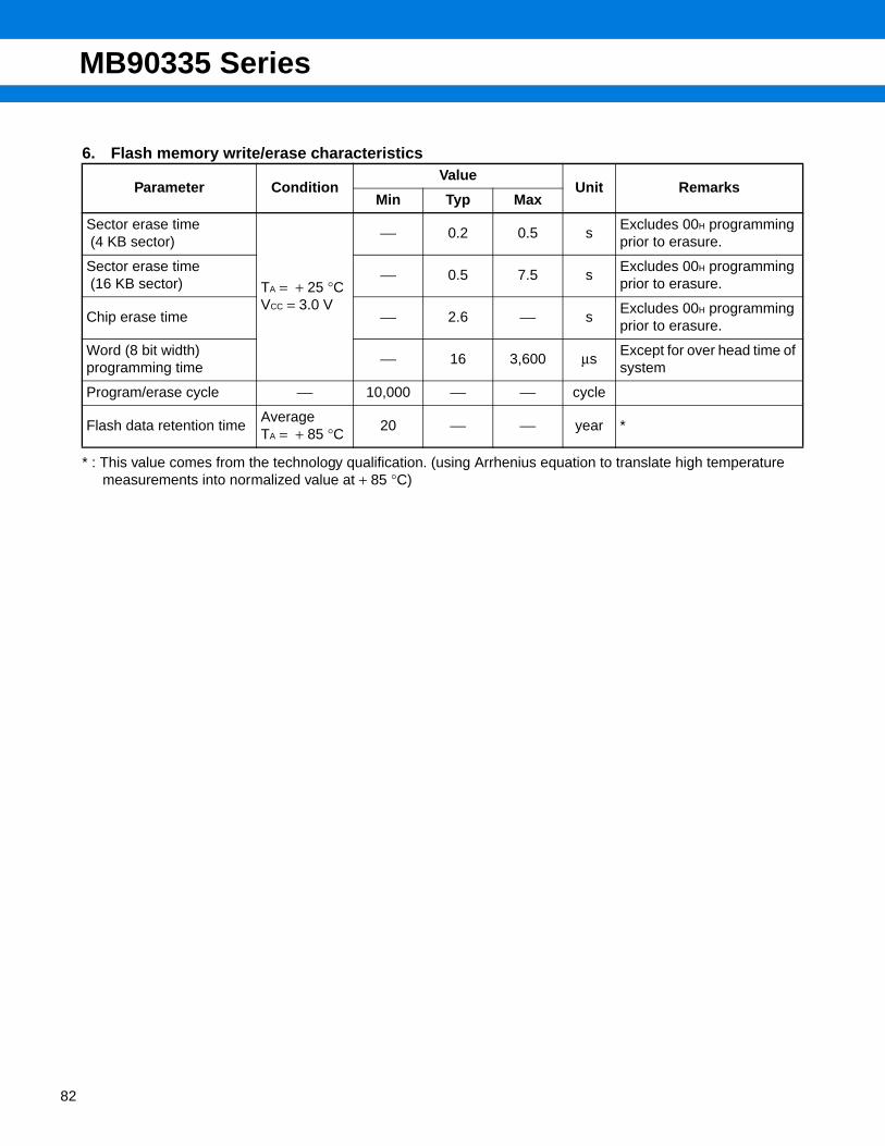
MB90335 Series
82
6. Flash memory write/erase characteristics
* : This value comes from the technology qualification. (using Arrhenius equation to translate high temperature measurements into normalized value at + 85 °C)
Parameter ConditionValue
Unit RemarksMin Typ Max
Sector erase time (4 KB sector)
TA = + 25 °CVCC = 3.0 V
⎯ 0.2 0.5 sExcludes 00H programming prior to erasure.
Sector erase time (16 KB sector)
⎯ 0.5 7.5 sExcludes 00H programming prior to erasure.
Chip erase time ⎯ 2.6 ⎯ sExcludes 00H programming prior to erasure.
Word (8 bit width) programming time
⎯ 16 3,600 µsExcept for over head time of system
Program/erase cycle ⎯ 10,000 ⎯ ⎯ cycle
Flash data retention timeAverageTA = + 85 °C 20 ⎯ ⎯ year *
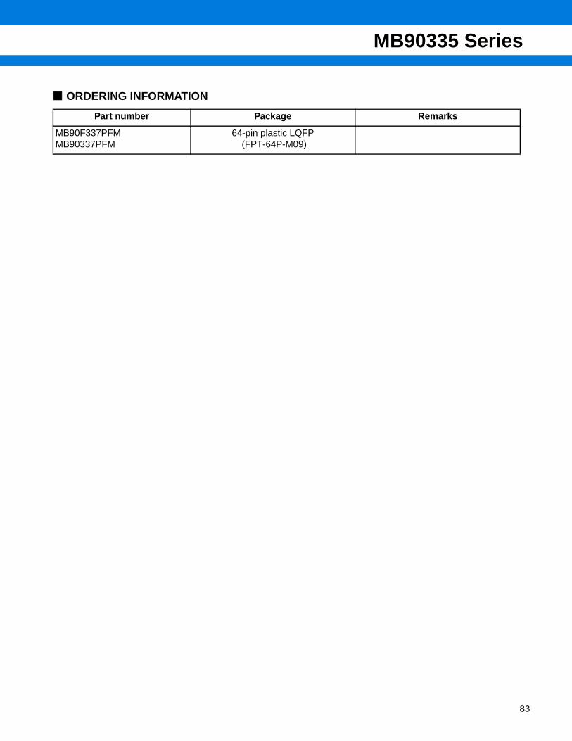
MB90335 Series
ORDERING INFORMATION
Part number Package Remarks
MB90F337PFMMB90337PFM
64-pin plastic LQFP (FPT-64P-M09)
83
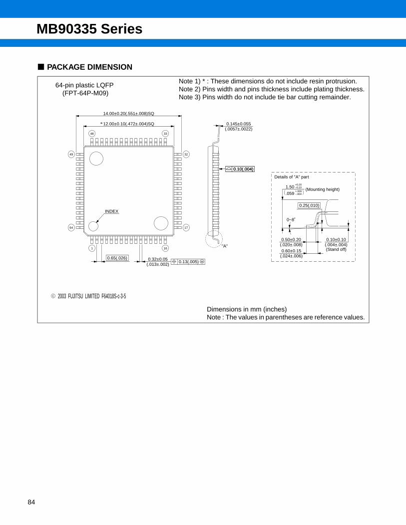
MB90335 Series
84
PACKAGE DIMENSION
64-pin plastic LQFP (FPT-64P-M09)
Note 1) * : These dimensions do not include resin protrusion.Note 2) Pins width and pins thickness include plating thickness.Note 3) Pins width do not include tie bar cutting remainder.
Dimensions in mm (inches) Note : The values in parentheses are reference values.
C 2003 FUJITSU LIMITED F64018S-c-3-5
0.65(.026)
0.10(.004)
1 16
17
3249
64
3348
12.00±0.10(.472±.004)SQ
14.00±0.20(.551±.008)SQ
INDEX
0.32±0.05(.013±.002)
M0.13(.005)
0.145±0.055(.0057±.0022)
"A"
.059 –.004+.008
–0.10+0.20
1.50
0~8˚
0.25(.010)
(Mounting height)
0.50±0.20(.020±.008)0.60±0.15
(.024±.006)
0.10±0.10(.004±.004)
Details of "A" part
(Stand off)
0.10(.004)
*
MB90335 Series
FUJITSU LIMITEDAll Rights Reserved.
The contents of this document are subject to change without notice. Customers are advised to consult with FUJITSU salesrepresentatives before ordering.The information, such as descriptions of function and applicationcircuit examples, in this document are presented solely for thepurpose of reference to show examples of operations and uses ofFujitsu semiconductor device; Fujitsu does not warrant properoperation of the device with respect to use based on suchinformation. When you develop equipment incorporating thedevice based on such information, you must assume anyresponsibility arising out of such use of the information. Fujitsuassumes no liability for any damages whatsoever arising out ofthe use of the information.Any information in this document, including descriptions offunction and schematic diagrams, shall not be construed as licenseof the use or exercise of any intellectual property right, such aspatent right or copyright, or any other right of Fujitsu or any thirdparty or does Fujitsu warrant non-infringement of any third-party’sintellectual property right or other right by using such information.Fujitsu assumes no liability for any infringement of the intellectualproperty rights or other rights of third parties which would resultfrom the use of information contained herein.The products described in this document are designed, developedand manufactured as contemplated for general use, includingwithout limitation, ordinary industrial use, general office use,personal use, and household use, but are not designed, developedand manufactured as contemplated (1) for use accompanying fatalrisks or dangers that, unless extremely high safety is secured, couldhave a serious effect to the public, and could lead directly to death,personal injury, severe physical damage or other loss (i.e., nuclearreaction control in nuclear facility, aircraft flight control, air trafficcontrol, mass transport control, medical life support system, missilelaunch control in weapon system), or (2) for use requiringextremely high reliability (i.e., submersible repeater and artificialsatellite).Please note that Fujitsu will not be liable against you and/or anythird party for any claims or damages arising in connection withabove-mentioned uses of the products.Any semiconductor devices have an inherent chance of failure. Youmust protect against injury, damage or loss from such failures byincorporating safety design measures into your facility andequipment such as redundancy, fire protection, and prevention ofover-current levels and other abnormal operating conditions.If any products described in this document represent goods ortechnologies subject to certain restrictions on export under theForeign Exchange and Foreign Trade Law of Japan, the priorauthorization by Japanese government will be required for exportof those products from Japan.
F0411© 2004 FUJITSU LIMITED Printed in Japan