fabrication of oxide nanostructures on glass by...
TRANSCRIPT

Surface and Coatings Technology 169–170(2003) 190–194
0257-8972/03/$ - see front matter� 2003 Elsevier Science B.V. All rights reserved.PII: S0257-8972Ž03.00057-4
Fabrication of oxide nanostructures on glass by aluminum anodizationand sol–gel process
S.Z. Chu*, K. Wada, S. Inoue, S. Todoroki
Advanced Materials Lab., National Institute for Materials Science, Namiki 1-1, Tsukuba, Ibaraki 305-0044, Japan
Abstract
A novel process of fabricating various oxide nanostructures on glass substrates is described. Transparent porous alumina films(� 6–150 nm) were first formed in acid solutions by anodization of aluminum layers sputter-deposited on a glass plate coatedwith a tin-doped indium oxide film. The porous alumina structures after pore-widened were then used as a host or a template ina sol–gel process to synthesize hollow or solid titania nanostructures within the nanopores, depending on the pore size of filmsand the affinity of the TiO gel to alumina films. Finally, titania nanotubules(;� 200 nm) or nanofibers(;� 50 nm) arrays2
on glass were fabricated after the anodic alumina films were selectively removed.� 2003 Elsevier Science B.V. All rights reserved.
Keywords: Titania nanotubules and nanofibers; Aluminium anodization; Sol–gel process
1. Introduction
Nanostructured materials have attracted a great inter-est in their potential applications in various fields suchas electronics, magnetism, optics and energy storage orexchange, etc. A variety of nanostructures(nanotubules,nanofibers) had been synthesized upon a template-method w1,2x using commercial porous alumina mem-branes produced by anodization of aluminum plates orfoils w3,4x. However, many concrete problems such asassembly and recycling of the nanostructures in manu-facturing practical devices have not been well solvedyet. Therefore, in the present study, we tried to create anovel nanotechnology to fabricate various nanostructuresdirectly on glass substrates by combining anodization ofsputtered aluminum with a sol–gel process. This tech-nology is expected to be applied in manufacturingpractical devices or functional glass for photocatalysisandyor solar energy systems.
2. Experimental
The fabrication procedure of oxide nanostructures onglass is schematically shown in Fig. 1: aluminum is firstdeposited on a glass substrate with a transparent and
*Corresponding author. Tel.:q81-298-51-3354; fax:q81-298-54-9060.
E-mail address: [email protected](S.Z. Chu).
conductive tin-doped indium oxide(ITO) film (a); aporous alumina structure is then formed on the glasssubstrate by anodization(b); after pore-widening toenlarge the pores and remove the barrier layer, theporous alumina structure is used as a host or a templateto synthesize various TiO materials(hollow or solid)2
within the nanopores by a sol–gel process, forming analumina–titania composite layer(c); various nanostruc-tures (tubules or fibers) on glass substrates are finallyfabricated after the anodic alumina is removed byselective chemical etching(d).
Highly pure aluminum film(99.99%, 1.5–2.0mm)deposited on a soda lime glass substrate with an ITO(10 Vyh, ;100 nm) film by a RF-sputtering was usedas specimens. Anodization was carried out potentiostat-ically in solutions of phosphoric(10%, 60–150 V, 277–283 K), oxalic (3%, 40 V, 293 K) or sulfuric (10%, 15V, 283 K) acid, respectively. To enlarge the pore size,the anodized specimens were immersed in a 5% phos-phoric acid solution for 5–45 min. In sol–gel coating,the porous alumina structures were first dipped in aTiO sol (;5% wt.) at room temperature for 10–202
min and then heated at 673 K for 2 h for the crystalli-zation of anatase TiO . Details for the synthesis method2
of TiO sol were described elsewherew5x. Titania nan-2
otubules arrays on glass were achieved by mechanicalabrasion and chemical etching in a solution of 5%H PO and 3% CrO at 353 K for 5 min.3 4 3
191S.Z. Chu et al. / Surface and Coatings Technology 169 –170 (2003) 190–194
Fig. 1. Scheme of fabrication procedure of nanostructures on ITOyglass substrates.
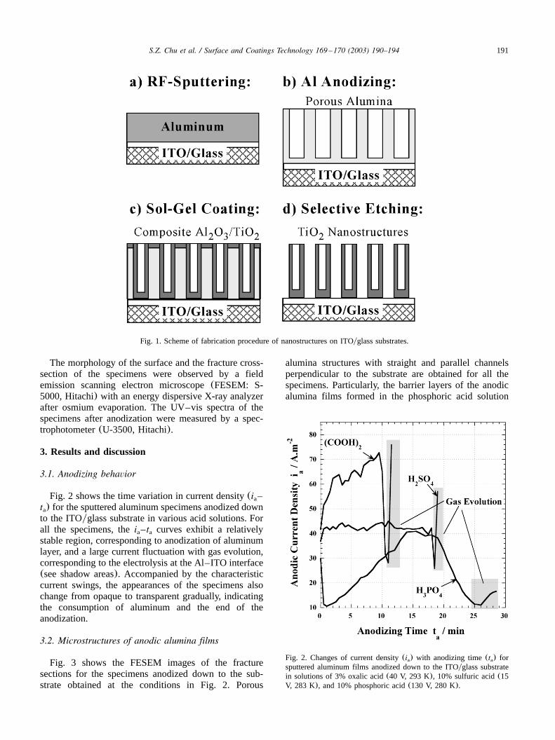
Fig. 2. Changes of current density(i ) with anodizing time(t ) fora a
sputtered aluminum films anodized down to the ITOyglass substratein solutions of 3% oxalic acid(40 V, 293 K), 10% sulfuric acid(15V, 283 K), and 10% phosphoric acid(130 V, 280 K).
The morphology of the surface and the fracture cross-section of the specimens were observed by a fieldemission scanning electron microscope(FESEM: S-5000, Hitachi) with an energy dispersive X-ray analyzerafter osmium evaporation. The UV–vis spectra of thespecimens after anodization were measured by a spec-trophotometer(U-3500, Hitachi).
3. Results and discussion
3.1. Anodizing behavior
Fig. 2 shows the time variation in current density(i –a
t ) for the sputtered aluminum specimens anodized downa
to the ITOyglass substrate in various acid solutions. Forall the specimens, thei –t curves exhibit a relativelya a
stable region, corresponding to anodization of aluminumlayer, and a large current fluctuation with gas evolution,corresponding to the electrolysis at the Al–ITO interface(see shadow areas). Accompanied by the characteristiccurrent swings, the appearances of the specimens alsochange from opaque to transparent gradually, indicatingthe consumption of aluminum and the end of theanodization.
3.2. Microstructures of anodic alumina films
Fig. 3 shows the FESEM images of the fracturesections for the specimens anodized down to the sub-strate obtained at the conditions in Fig. 2. Porous
alumina structures with straight and parallel channelsperpendicular to the substrate are obtained for all thespecimens. Particularly, the barrier layers of the anodicalumina films formed in the phosphoric acid solution

192 S.Z. Chu et al. / Surface and Coatings Technology 169 –170 (2003) 190–194
Fig. 3. FESEM images of vertical fracture sections of anodic alumina films formed in solutions of(a) phosphoric acid,(b) oxalic acid and(c)sulfuric acid. Insert in(c) is the transverse fracture section of the film. Anodizing conditions are the same as in Fig. 2.

193S.Z. Chu et al. / Surface and Coatings Technology 169 –170 (2003) 190–194
Fig. 4. UV-infrared transmittance spectra for the specimens anodizedat different acid solutions. Anodizing conditions are the same as inFig. 2.
Fig. 5. FESEM images of fracture section for specimens dip-coated in a TiO sol and heated at 673 K for 2 h. Fabrication conditions:(a) 10%2
H PO , 150 V, 277 K,t s45 min, t s20 min; (b) 3% oxalic acid, 40 V, 293 K;t s15 min, t s10 min.3 4 p.w dip p.w dip
(Fig. 3a) exhibit an arched shape with a thin thicknessof 1y4–1y3 of the pore walls, which may be caused bythe local increases of temperature andyor acidity at thepore bases during anodization of the Al–ITO interfacew6x. The average pore sizes and pore spacing of theanodic alumina films are approximately 150 and 350nm, 30 and 100 nm, and 6 and 50 nm for phosphoric,oxalic and sulfuric acid solutions, respectively. Corre-spondingly, through appropriate chemical dissolutions,the pores can be widened to;� 200,;� 50 and;�20 nm, respectively.
3.3. Transparency of anodic alumina films
The transparency of materials is an important param-eter for applications in photocatalysis and photocellsystems. Fig. 4 shows the UV-infrared transmittancespectra for the specimens anodized in different solutions.The average transmittances of all the anodized speci-mens are close to that of the ITOyglass substrate(dotline), indicating that the alumina films are all transparentthrough UV–visible range, due to the consumption ofaluminum by anodization. In visible light range, theinterference patterns in the spectra are similar, irrespec-tive of the pore size and the sort of the films; while innear infrared region(shadow area) and UV range(insert), the interference fluctuation in the spectra wouldinfer some dependence upon the pore sizes andyor thesorts of alumina films.
3.4. Synthesis of titania nanostructures
In sol–gel process, the TiO is filled into the pores2
of the anodic alumina films driven by the capillaryeffect. Fig. 5 displays the fracture sections for thespecimens after dip-coating in the TiO sol and heated2
at 673 K for 2 h. For the films formed in phosphoricacid solution(Fig. 5a), the TiO sol enters the nanopores2
along the walls of anodic alumina films and connectsdirectly to the substrate. After being dried and heated,the TiO layer adheres to the pore walls because of its2
good affinity to the alumina film, thus forming a hollowTiO -coated nanostructure with a large surface area. For2
the oxalic-anodized alumina films(Fig. 5b), on theother hand, the resultant TiO is in the form of a solid2
structure with many voids inside and with poor adher-ence to the alumina wall(see arrows). As for thesulfuric-anodized film, TiO sol could not enter the2
pores of the films, probably because of the small pore

194 S.Z. Chu et al. / Surface and Coatings Technology 169 –170 (2003) 190–194
Fig. 6. Titania nanotubules array(;�200 nm=40 nm=3 mm) standing on an ITOyglass substrate(Anodization: 10% H PO , 150 V, 277 K;3 4
Pore-widening: 45 min).
size (;� 20 nm) in the film andyor the viscosity andthe surface tension of the TiO sol adopted.2
Fig. 6 gives an example of TiO nanotubules array2
on the glass substrate. The TiO nanotubules,;� 2002
nm for outer diameter,;� 40 nm thick and;3 mmlong, stand straight on the ITOyglass substrate withcertain spaces among each other, thus giving a verylarge surface area that may be incomparable for conven-tional TiO layers. Moreover, according to XRD analysis2
and TEM observation(not shown), the TiO nanotubules2
are polycrystalline anatase and composed of 4–20 nmgrains, which are known to be associated to the goodphotocatalytic performances.
4. Conclusions
Various oxide nanostructures, highly porous aluminafilms (� 6–150 nm) and TiO yAl O layers(;� 1202 2 3
nm), well-arranged TiO nanotubules arrays(;� 2002
nm), and TiO nanofibers(;� 50 nm) on ITOyglass2
substrates were fabricated by combining techniques of
aluminum anodization and a sol–gel process. The resul-tant nanostructures, especially the porous TiOyAl O2 2 3
composite layers and TiO nanotubule arrays synthesized2
upon phosphoric-anodized films, possess large surfaceareas and are mechanically strong with good adherenceto the substrate. Therefore, it is reasonable to considerthe TiO nanostructures as a promising nanomaterial in2
the manufacture of practical devices for photocatalysisand photocells system, which are being explored.
References
w1x C.R. Martin, Science 266(1994) 1961.w2x B.B. Lakshmi, P.K. Dorhout, C.R. Martin, Chem. Mater. 9
(1997) 857.w3x R.C. Furneaux, W.R. Rigby, A.P. Davidson, Nature 337(1989)
147.w4x H. Masuda, K. Fukuda, Science 268(1995) 1466.w5x S.Z. Chu, K. Wada, S. Inoue, S. Todoroki, Chem. Mater. 14
(2002) 266.w6x S.Z. Chu, K. Wada, S. Inoue, S. Todoroki, J. Electrochem.
Soc. 149(7) (2002) B321.