simple fabrication of one-dimensional metal nanostructures
TRANSCRIPT

ANALYTICAL SCIENCES JANUARY 2014, VOL. 30 151
1 Introduction
Surface enhanced Raman scattering (SERS) is an interesting process in which normally weak Raman signals can be amplified by many orders of magnitude.1 This impressive phenomenon is
mainly caused by an enhanced, light-induced electric field at the surface of a metallic nanoparticle (MNP). When the incident light is in resonance with the oscillations of conduction electrons in a MNP, all of the conduction electrons are driven to oscillate collectively in an optical phenomenon, called localized plasmon resonances (LPRs).2–4 LPRs are responsible for the strong light scattering and absorption of MNPs, as well as for generating enhanced local electric fields on the surface of MNPs at sites known as “hot spots”. Molecules within hot spots experience strong interactions, with the degree of enhancement being determined by multiple factors, and in some cases, single molecule detection is possible.5–7 The maximum enhancement has been reported to range from 106 to 107 for isolated single MNPs, such as Au or Ag.8 Furthermore, closely spaced MNPs have been shown to provide an enhancement of up to 1011 at the gap between two particles.9 Thus, arrays consisting of precise assemblies and patterning of MNPs as SERS substrates are helpful in SERS studies.
The ability to produce arrays with homogeneous particle sizes and shapes as well as regular interparticle spacing using lithography techniques, called the “top-down process”, has provided important insights into the SERS mechanism in
2014 © The Japan Society for Analytical Chemistry
E-mail: [email protected]
1 Introduction 1512 Direct Observations of LPRs of MNPs
with Optical Microscopy 1523 One-dimensional (1D) Plasmon Coupling in
Metallic Nanofibers Prepared by Evaporation- induced Self-assembly with DNA 153
4 Applications of Metallic Nanofibers for SERS Analysis 154
5 Conclusions 1556 Acknowledgements 1557 References 156
Simple Fabrication of One-Dimensional Metal Nanostructures and Their Application for SERS Analysis
Hidenobu NAKAO
National Institute for Materials Science, 1-1 Namiki, Tsukuba, Ibaraki 305–0044, Japan
This review highlights work using the author’s method for the preparation of highly aligned metallic nanofibers with one-dimensional aggregates of metal nanoparticles (MNPs) and their utilization in surface enhanced Raman scattering (SERS) analysis. The preparation method, which is based on the process of evaporation-induced self-assembly with DNA and a drying front movement, eliminates the need for lithography and an external field; it is also fast, cheap and easy. Dark-field scattering spectroscopy was used to study the strong plasmon coupling of MNPs in metallic nanofibers. Furthermore, Raman spectral imaging of the metallic nanofibers revealed the existence of intense hot spots localized along their axes, which played a significant role in the intensity of SERS signals from DNA bases and rhodamine B in the metallic nanofibers. Our results demonstrate the use of evaporation-induced self-assembly with DNA as a straightforward method to produce the one-dimensional coupling of localized plasmons with a longer scale, and to facilitate the fabrication of optical sensor chips for single-molecule detection via SERS.
Keywords Metal nanoparticle, metal nanoarray, dark-field optical microscopy, SERS, Raman imaging, localized plasmon resonance
(Received September 3, 2013; Accepted September 25, 2013; Published January 10, 2014)
Hidenobu NAKAO received his Ph.D. degree in 1997 from Yamaguchi University. He worked at Japan Chemical Innovation Institute as a research fellow of the New Energy and Industrial Technology Development Organization (1997 – 2001). He also worked at National Food Research Institute as a research fellow (2001 – 2003) and as a research fellow at the Japan Society for the Promotion of Science (2003 – 2005). He is currently a senior researcher at the National Institute for Material Sciences.
His current research interest is the development and construction of opto-electronic devices with nanomaterials and biomolecules.
Reviews
152 ANALYTICAL SCIENCES JANUARY 2014, VOL. 30
ordered MNP structures.10–12 However, it is difficult to reproducibly fabricate gaps of only a few nanometers, which result in even larger electric fields, using e-beam lithography. On the other hand, in self-assembled nanostructures of chemically prepared MNPs, as in the “bottom-up process”, the length and the density of the surface capping molecules determine the minimum interparticle spacing. In particular, various MNPs under slow and irreversible evaporation form well-ordered, self-assembled MNP patterns on surfaces, resulting in a simple, cheap and robust strategy for self-assembly.13–18
Here, we highlight our efforts toward a simple approach for the preparation of metallic nanofibers consisting of MNPs self-assembled into DNA on surfaces and spectroscopic
investigations of their SERS enhancement. We aim to present a simple and reproducible method for creating metallic nanofibers without any special equipment, realizing facile observations of one-dimensional (1D) plasmon coupling with long-range order. In our assembly of MNPs, highly aligned DNA nanofibers on a surface are used as a 1D template, and can be driven by a simple interface (air–liquid) movement. Using dark-field optical microscopy, we have directly observed strong near-field plasmon coupling in metallic nanofibers, resulting in the visualization of “hot spots” for enhancing SERS. Finally, applications for SERS analysis that take advantage of localized electric fields on prepared metallic nanofibers are discussed.
2 Direct Observations of LPRs of MNPs with Optical Microscopy
In general, single MNPs or MNP structures can be visualized using high-resolution techniques, such as scanning electron microscopy (SEM), transmission electron microscopy (TEM) and atomic force microscopy (AFM). For MNPs such as Au and Ag, their LPRs fall into the visible and near-infrared regions of the electromagnetic spectrum. Significant consequences of this are the bright colors exhibited by particles both in transmitted and reflected light, due to resonantly enhanced absorption and scattering. Thus, LPRs of MNPs as a function of particle size, particle shape, aggregation state, and local environment can be readily visualized as various true colors by using conventional optical microscopy.
In optical microscopy, dark-field illumination is used to enhance the contrast associated with light scattered from MNPs (Fig. 1). In Fig. 1a, only the light scattered by the structure under study is collected in the detection path, while directly transmitted light is blocked using a dark-field condenser.19 In Fig. 1b, by using index matched interface arrangements, the illumination system provides very high contrast, since only light scattering by MNPs is back collected by the objective, while surface defects and other imperfections are invisible due to index matching.20 Total internal reflection (TIR) with prism coupling is also available, as shown in Fig. 1c.21 Since the evanescent field generated from TIR at a dielectric boundary is a near-field effect, it provides a convenient excitation source while only exciting MNPs very closed to the interface. The advantage of these dark-field illuminations is the low light levels in the background, enhancing only light scattering from specimens.
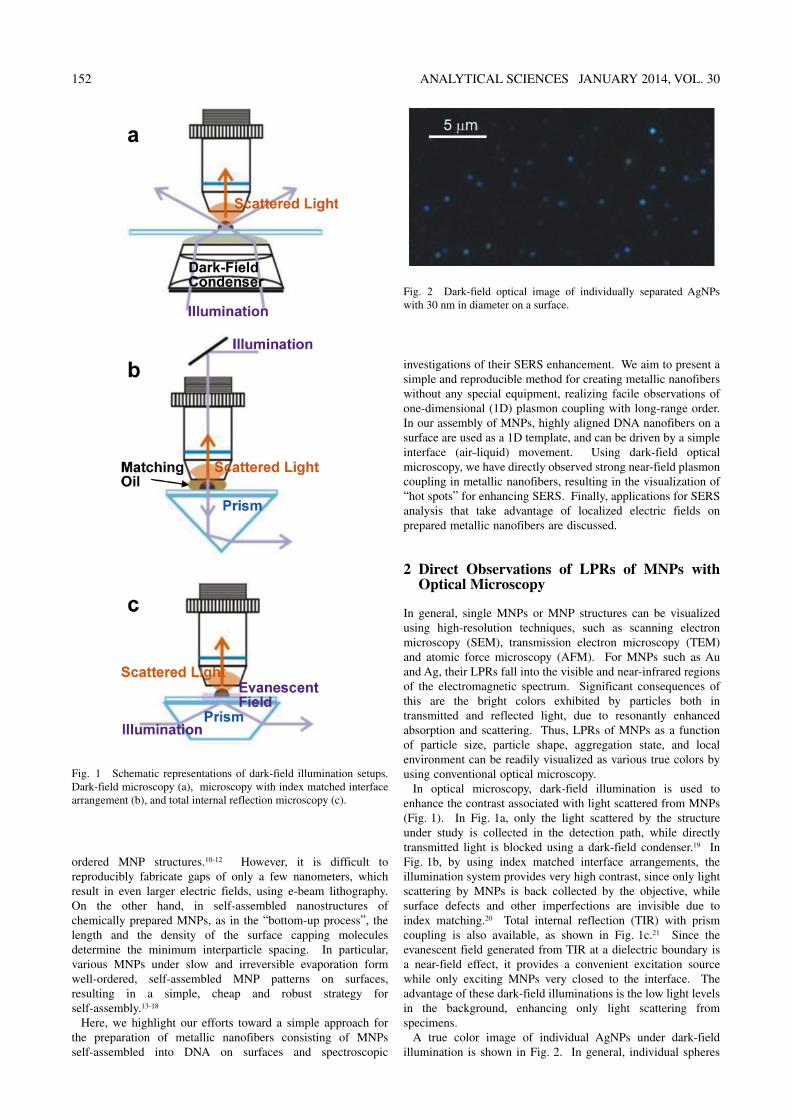
A true color image of individual AgNPs under dark-field illumination is shown in Fig. 2. In general, individual spheres
Fig. 1 Schematic representations of dark-field illumination setups. Dark-field microscopy (a), microscopy with index matched interface arrangement (b), and total internal reflection microscopy (c).
Fig. 2 Dark-field optical image of individually separated AgNPs with 30 nm in diameter on a surface.

ANALYTICAL SCIENCES JANUARY 2014, VOL. 30 153
of AgNPs are observed as blue spots, originating from their LPR colors.22 The LPR colors of MNPs under scattered light are also affected by their size, shape and aggregation.19,22–24 However, the resolution in dark-field illumination is under the diffraction limit, in common with conventional optical microscopy. Consequently, when MNPs are sparsely dispersed on a surface, the above setups enable the study of single MNPs. Some studies have investigated LPRs in MNPs with different shapes by using dark-field microscopy and SEM.24 For spectral investigations, the scattered light from single MNPs is readily focused by the microscope onto the spectrometer. These dark-field spectroscopic techniques allow us to measure spectra with very little background light.
By using an optical microscopy technique, such as the above dark-field illumination, MNPs can be also used as probes in cellular imaging.25–27 Most recently, we have reported that AuNPs can be used as localization markers to visualize particle absorption through Caco-2 cells using dark-field optical microscopy.27 Since AuNPs attached to the cell surface have their own LPR colors, the locations of individual AuNPs could be distinguished from the white network of tight junctions in the same field of view under a microscope. Unlike fluorescent dyes, MNPs do not have trouble with photobleaching or blinking, and can give stronger and more stable signals. Dark-field microscopy with MNPs as probes is a very simple yet effective technique, and is well suited for uses involving live and unstained biological samples.
3 One-dimensional (1D) Plasmon Coupling in Metallic Nanofibers Prepared by Evaporation-induced Self-assembly with DNA
In observations and analyses with optical microscopy, forming ordered arrays of MNPs on a solid surface enables easy observation. Recently, we have developed a simple method to create highly aligned DNA nanofibers on a surface.28 This method is based on the processes of solvent vapor-induced buildup and controlling the drying front movement, and forms parallel aligned DNA nanofibers exceeding several hundreds of micrometers in length and 40 nm in diameter on a poly(dimethylsiloxane) (PDMS) sheet. Thus, this process leads to DNA nanostrands that are much longer than the contour
length of λ-DNA (16.3 μm), and facilitates manipulation of a single nanofiber under microscopic observation, while measuring its electrical and optical properties, and connecting it to electrode pads. Various MNPs could also be attached to such nanofibers, forming metallic nanofibers with a longer scale.29–31
Figure 3 is a dark-field optical micrograph showing metallic nanofibers with AuNPs (30 nm in diameter) on a PDMS sheet. In general, individual spheres of AuNPs are observed as green particles, originating from their LPR colors. When MNPs are organized in closely spaced arrays, their LPR peak is shifted towards lower energy, and an increase in the bandwidth is observed because the dielectric constant of the surrounding MNPs is increased. Thus, the many reddish lines originating from their LPRs indicate that many AuNPs are assembled along DNA nanofibers. Although the curvature of the lines at the edges of the surface is due to the shape of the meniscus movement, they are aligned parallel to the moving drying front of the solvent. Metallic nanoarrays also exceed several hundred micrometers in length, and can be made within 30 min. Figure 3c is a SEM image showing the morphology of metallic nanofibers with AuNPs, which indicates that dense packing of AuNPs 30 nm in diameter is realized.
We also observed dark-field optical images of our metallic nanofibers under polarized light.29,30 The scattered light intensity from metallic nanofibers is stronger when the light is polarized parallel to the arrays, while it is weaker for vertical polarization. Furthermore, the scattering intensity exhibits a cosine-like dependence on the polarization angle. The enhancement of the light field localized in gaps between MNPs also strongly depends on the incident light polarization.3,4 For a uniaxial alignment of ordered MNPs, polarization parallel to the uniaxial alignment enhances light field localization in gaps between MNPs, leading to strong light scattering from ordered MNPs. In contrast, polarization vertical to the uniaxial alignment does not enhance light field localization.
Since it is well known that the enhancement of a light field localized on the surface of AgNPs is much larger than that for AuNPs,32–34 using AgNPs is expected to result in stronger plasmon coupling in the metallic nanofibers. Most recently, we have also prepared metallic nanofibers with AgNPs (8 nm in diameter).31 These also showed strong 1D coupling of plasmons similar to the case for AuNPs. In addition, we found that the number of particle aggregations along metallic nanofibers
Fig. 3 Dark-field scattering images of metallic nanofibers prepared by evaporation-induced self-assembly with DNA. Large area image of metallic nanofibers (a). Enlarged image with a 100× objective (b). SEM image of metallic nanofiber (c).

154 ANALYTICAL SCIENCES JANUARY 2014, VOL. 30
increased with increasing AgNP concentration, which was indicated by a color change (red shift) and homogenization in the light scattering. Furthermore, depending on the polarization direction of the exiting light, this leads to a blue shift in the LPR for the excitation of transverse modes, and a red shift for longitudinal modes. The spectrum obtained under excitation parallel to the nanofiber exhibits a maximum peak at 750 to 800 nm, whereas that under perpendicular polarization exhibits a maximum peak at 500 nm. The polarization dependence of the two plasmon modes in the nanofiber scattering spectra reveals that the plasmon coupling preferentially occurs in a quasi-one-dimensional direction along the nanofiber axis,3,35,36 which is similar to LPRs observed for long nanorods or nanowires.37–39
4 Applications of Metallic Nanofibers for SERS Analysis
Our highly anisotropic metallic nanofibers would be expected to produce highly localized light fields for enhancing SERS. Termed “hot spots”, these highly confined fields enable an increased interaction between the molecules and electromagnetic fields. This also leads to the possibility of imaging. Raman or SERS imaging can provide high throughput chemical information with spatial distributions of analytes with a resolution in micrometers40 or several tens of nanometers.41 In order to study the SERS effect on our metallic nanofibers, Raman scattering spectral images were obtained using a laser Raman microscope with an excitation wavelength of 532 nm.31 The Raman spectra of metallic nanofibers with well-attached AgNPs (9 ng mL–1) exhibited many intense bands in the 1000 – 1600 cm–1 region, which are thought to arise from DNA bases (A, T, G and C). On the other hand, for metallic nanofibers with insufficiently attached AgNPs (1.5 ng mL–1), the Raman
image indicated weaker intensities and intermittent distributions along the nanofiber. Using unattached regions of the nanofibers as a reference, well-attached AgNPs were found to enhance the Raman scattering signal by a factor of >103.
However, sequential SERS spectra observed from metallic nanofibers showed variations. These different shifts in Raman frequencies might indicate that the different conformational states of DNA molecules at different concentrations probably influence the Raman frequencies.42 Changes in the backbone structure from the B-form to the A-form would have a strong effect on the orientation of DNA bases on surfaces of AgNPs.43,44 Consequently, for confirming SERS effects on our metallic nanofibers, the use of DNA bases as probe molecules is not convenient. Instead, we tried to observe SERS effects of metallic nanofibers using rhodamine B (RB) as a probe molecule. The PDMS substrate with metallic nanofibers was then exposed to 10–6 M R6G in Milli-Q water for 30 min. The substrate was exposed to Milli-Q water for 5 min to remove RB in solution.
Figure 4 shows a Raman image analysis of a single metallic nanofiber before and after the introduction of a 10–6 M RB solution. From a comparison of Figs. 4a and 4b, it is striking that the Raman image along the nanofibers indicated stronger intensities and more uniform distributions along the nanofiber after the introduction of RB. As described above, the sequential SERS spectra observed from metallic nanofibers before the introduction of RB show large differences because of different conformational states of DNA molecules (Fig. 4c). In Fig. 4d, after the metallic nanofibers were exposed to a 10–6 M RB solution, spectral features characteristic of RB at 607, 768, and 1196 cm–1 associated with the C–C–C ring in-plane, out-of-plane bending, and C–C stretching vibrations, respectively, as well as bands 1362, 1542, 1653 cm–1, at which are usually assigned to aromatic C–C stretching vibrations of the RB molecule.45,46 SERS spectra of RB obtained at all points along the metallic
Fig. 4 Raman scattering spectra obtained at different points in Raman images of metallic nanofibers before and after introduction of RB. Raman images of metallic nanofibers before (a) and after exposure to 10–6 M RB solution (b). The image (a) was obtained using 20 μW 532 nm laser radiation of 10 s/line. The image (b) were obtained using 10 μW 532 nm laser radiation of 3 s/line. Raman spectra (c) and (d) obtained at points 1 – 4 in images, (a) and (b), respectively. Spectra were vertically offset for clarity.

ANALYTICAL SCIENCES JANUARY 2014, VOL. 30 155
nanofiber, as shown in Fig. 4d, were almost the same expect for the peak intensities. It is important that as can be seen in Figs. 4c and 4d, SERS signals of RB are detectable for shorter exposure times (3 s/line) and lower excitation power (10 μW) than those for DNA bases. Since DNA molecules with a double-strand structure have rigid and larger structures, the junction sites of two or more particles, called “hot spots”, would not be fully filled with DNA bases. Consequently, it seems reasonable that smaller RB molecules would penetrate into empty “hot spots”, resulting in an increase in its SERS signals. The differences in SERS intensity at points on the metallic nanofiber are attributed to the morphology of the metallic nanofiber with different aggregation levels of AgNPs. By varying the particle sizes and surface properties of AgNPs, metallic nanofibers with homogeneous aggregations of AgNPs could be controlled, which would achieve more efficient SERS. The influence of the DNA matrix in metallic nanofibers on SERS signals can be suppressed by the exposure time and laser power, and such an influence must be removed in orfer to detect the analyte molecules. Soft etching, such as UV/ozone or plasma treatment for metallic nanofibers, would achieve the conversion to metallic arrays without organic compounds.
At present, the prepared metallic nanofibers are linear, but placed randomly on the substrate. By creating the appropriate relief pattern on PDMS, and properly modifying the substrate surfaces, it is possible to control the location of nanofiber generation. Our metallic nanofibers can also be restructured by the transfer-printing (TP) technique, and integrated into the desired position on various substrates, such as glass or silicon.26,28 Figure 5 presents dark-field micrographs of 2D metallic nanofiber patterns. The image is clearly reddish when the light is polarized parallel to the fibers, while vertically aligned metallic nanofibers are bluish (Figs. 5(b) and 5(c)). The above result also indicates that 1D arrangements of particles in the metallic nanofiber are maintained after the TP process. The main advantages of TP are that the metallic nanofibers can be printed in the desired positions on the substrate and that various detection sites can be printed on the same substrate by stamping PDMS sheets with different metallic nanofibers modified with
various materials. Therefore, our method will advance the fabrication of nano-optical devices and optical sensor chips for single-molecule detection.
5 Conclusions
In this review, we have summarized our recent work on a simple preparation method for metallic nanofibers and their application to SERS analysis. Our approach can be used as a general method for the growth and patterning of metallic nanofibers with highly localized light fields. In addition, our metallic nanofibers produce strong near-field plasmon coupling of MNPs for enhancing the SERS effect. A combined dark-field imaging and optical spectroscopy approach was particularly useful for understanding the LPRs of one-dimensionally coupled MNPs in the metallic nanofibers. In the field of analytical chemistry, one promising application is in optical sensors, where single-molecule detection via SERS has been reported. The shape of MNPs has an effect on localized light fields; for example, the enhanced light fields are localized at the corners of nanocubes and are much larger compared with nanospheres. Controlling LPRs is the key to optimizing SERS, since plasmon resonances are responsible for generating the strong local light fields necessary for SERS. In terms of controlling the LPRs, shape engineering of nanoparticles has provided an efficient handle. The manipulation of hot spots through shape-controlled synthesis and self-assembly with our method could lead to the advancement of SERS. Our metallic nanofibers could also be restructured by the TP technique, and integrated into a desired position on various substrates, such as glass or silicon. Therefore, our method will advance the fabrication of optical sensor chips for single-molecule detection.
6 Acknowledgements
The authors would like to thank Dr. H. T. Miyazaki for many most useful and inspiring scientific discussions. This work was
Fig. 5 Procedure of TP process for creating a 2D pattern of metallic nanofibers (a). Polarized dark-filed optical microscopy images of 2D metallic nanofibers, (b) and (c). Arrows indicate the directions of light polarization.

156 ANALYTICAL SCIENCES JANUARY 2014, VOL. 30
partially supported by a Grant-in-Aid for Scientific Research (B) and (C) from the Ministry of Education, Science, Sports and Culture, Japan (Nos. 23360068 and 22550136). This study was also supported by the ‘‘Nanotechnology Network Project’’ of the Ministry of Education, Culture, Sports, Science and Technology (MEXT), Japan.
7 References
1. M. Moskovits, J. Raman Spectrosc., 2005, 36, 485. 2. C. L. Haynes, C. R. Yonzon, X. Zhang, and R. P. V. Duyne,
J. Raman Spectrosc., 2005, 36, 471. 3. S. A. Maier, “Plasmonics: Fundamentals and Application”,
2007, Springer Science+Business Media LLC. 4. M. Rycenga, P. H. C. Camargo, W. Li, C. H. Moran, and Y.
Xia, J. Phys. Chem. Lett., 2010, 1, 696. 5. A. Nakata, T. Nomoto, T. Toyota, and M Fujinami, Anal.
Sci., 2013, 29, 865. 6. M. Knauer, N. P. Ivleva, R. Niessner, and C. Haisch, Anal.
Sci., 2010, 26, 761. 7. K. Kneipp, H. Kneipp, R. Manoharan, I. Itzkan, R. R.
Dasari, and M. S. Feld, Bioimaging, 1998, 6, 104. 8. D. Pristinski, S. Tan, M. Erol, H. Du, and S. Sukhishvili, J.
Raman Spectrosc., 2006, 37, 762. 9. H. Xu, J. Aizpurua, M. Kaell, and P. Apell, Phys. Rev. E,
2000, 62, 4318.10. S. A. Maier, M. L. Brongersma, P. G. Kik, S. Meltzer, A. A.
G. Requichia, and H. Atwater, Adv. Mater., 2001, 13, 1501.11. M. Rycenga, P. H. C. Camargo, W. Li, C. H. Moran, and Y.
Xia, J. Phys. Chem. Lett., 2010, 1, 696.12. K. Ueno, S. Juodkazis, T. Shibuya, V. Mizeikis, Y. Yokota,
and H. Misawa, J. Phys. Chem. C, 2009, 113, 11720.13. L. Motte, F. Billoudet, D. Thiaudière, A. Naudon, and M.-P.
Pileni, J. Phys. III, 1997, 7, 517.14. S. A. Harfenist, Z. L. Wang, M. M. Alvarez, I. Vezmar, and
R. L. Whetten, Adv. Mater., 1997, 9, 817.15. P. N. Provencio, J. E. Martin, J. G. Odinek, and J. P.
Wilcoxon, Microsc. Microanal., 1998, 4, 734.16. P. C. Ohara, D. V. Leff, J. R. Heath, and W. M. Gelbart,
Phys. Rev. Lett., 1995, 75, 3466.17. R. D. Deegan, O. Bakajin, T. F. Dupont, G. Huber, S. R.
Nagel, and T. A. Witten, Nature, 1997, 389, 827.18. C. Zhang, X. Zhang, X. Zhang, X. Fan, J. Jie, J. C. Chang,
C.-S. Lee, W. Zhang, and S.-T. Lee, Adv. Mater., 2008, 20, 1716.
19. C. Sönnichsen, T. Franzl, T. Wilk, G. von Plessen, and J. Feldmann, Phys. Rev. Lett., 2002, 88, 077402.
20. M. Barbic, J. J. Mock, D. R. Smith, and S. Schultz, J. Appl. Phys., 2002, 91, 9341.
21. C. Sönnichsen, S. Geiner, N. E. Hecker, G. von Plessen, J. Feldmann, H. Ditlbacher, B. Lamprecht, J. R. Krenn, F. R.
Aussenegg, V. Z. Chan, J. P. Spatz, and M. Moller, Appl. Phys. Lett., 2000, 77, 2949.
22. R. Jin, Y. W. Cao, C. A. Mirkin, K. L. Kelly, G. C. Schatz, and J. G. Zheng, Science, 2001, 294, 1901.
23. J. J. Mock, D. R. Smith, and S. Schultz, Nano Lett., 2003, 3, 485.
24. H. Kuwata, H. Tamaru, K. Esumi, and K. Miyano, Appl. Phys. Lett., 2003, 83, 4625.
25. I. H. El-Sayed, X. Huang, and M. A. El-Sayed, Nano Lett., 2005, 5, 829.
26. L. Cognet, C. Tardin, D. Boyer, D. Choquet, P. Tamarat, and B. Lounis, Proc. Natl. Acad. Sci. U. S. A., 2003, 100, 11350.
27. T. Kobori, J. Watanabe, and H. Nakao, Anal. Sci., 2012, 28, 61.
28. H. Nakao, T. Taguchi, H. Shiigi, and K. Miki, Chem. Commun., 2009, 1858.
29. H. Nakao, H. Hayashi, H. Shiigi, and K. Miki, Anal. Sci., 2009, 25, 1177.
30. H. Nakao, Anal. Sci., 2009, 25, 1387.31. H. Nakao, S. Tokonami, T. Hamada, H. Shiigi, T. Nagaoka,
F. Iwata, and Y. Takeda, Nanoscale, 2012, 4, 6814.32. R. J. Stokes, A. Macaskill, P. J. Lundahl, W. E. Smith, K.
Faulds, and D. Graham, Small, 2007, 3, 1593.33. D. Graham, K. Faulds, and W. E. Smith, Chem. Commun.,
2006, 4363.34. D. Graham, D. G. Thompson, W. E. Smith, and K. Faulds,
Nat. Nanotechnol., 2008, 3, 548.35. W.-S. Chang, L. S. Slaughter, B. P. Khanal, P. Manna, E. R.
Zubarev, and S. Link, Nano Lett., 2009, 9, 1152.36. W.-S. Chang, B. Willingham, L. S. Slaughter, S.
Dominguez-Medina, P. Swanglap, and S. Link, Acc. Chem. Res., 2012, 45, 1936.
37. G. W. Bryant, F. J. G. de Abajo, and J. Aizpurua, Nano Lett., 2008, 8, 631.
38. E. R. Encina and E. A. Coronado, J. Phys. Chem. C, 2007, 111, 16796.
39. B. N. Khlebtsov and N. G. Khlebtsov, J. Phys. Chem. C, 2007, 111, 11516.
40. S. Preciado-Flores, D. A. Wheeler, T. M. Tran, Z. Tanaka, C. Jiang, M. Barboza-Flores, F. Qian, Y. Li, B. Chen, and J. Z. Zhang, Chem. Commun., 2011, 47, 4129.
41. J. Ando, K. Fujita, N. I. Smith, and S. Kawata, Nano Lett., 2011, 11, 5344.
42. T. Goto and H. Watarai, Anal. Sci., 2010, 26, 135.43. L. Sun, Y. Sun, F. Xu, Y. Zhang, T. Yang, C. Guo, Z. Liu,
and Z. Li, Nanotechnology, 2009, 20, 125502.44. J. M. Benevides and G. J. Thomas Jr, Nucleic Acids Res.,
1983, 11, 5747.45. D. Pristinski, S. Tan, M. Erol, H. Du, and S. Sukhishvili, J.
Raman Spectrosc., 2006, 37, 762.46. A. Kudelski, Chem. Phys. Lett., 2005, 414, 271.