fabrication of silicon and glass devices for microfluidic ... · fabrication of silicon and glass...
TRANSCRIPT

VTT P
UB
LICA
TION
S 670 Fabrication of silicon and glass devices for m
icrofluidic bioanalytical applicationsK
olari
ESPOO 2007ESPOO 2007ESPOO 2007ESPOO 2007ESPOO 2007 VTT PUBLICATIONS 670
Kai Kolari
Fabrication of silicon and glass devicesfor microfluidic bioanalyticalapplications
VTT PUBLICATIONS
649 Niskanen, Ilkka. An interactive ontology visualization approach for the domain ofnetworked home environments. 2007. 112 p. + app. 19 p.
650 Wessberg, Nina. Teollisuuden häiriöpäästöjen hallinnan kehittämishaasteet. 2007.195 s. + liitt. 4 s.
651 Laitakari, Juhani. Dynamic context monitoring for adaptive and context-awareapplications. 2007. 111 p. + app. 8 p.
652 Wilhelmson, Annika. The importance of oxygen availability in two plant-basedbioprocesses: hairy root cultivation and malting. 2007. 66 p. + app. 56 p.
653 Ahlqvist, Toni, Carlsen, Henrik, Iversen, Jonas & Kristiansen, Ernst. Nordic ICTForesight. Futures of the ICT environment and applications on the Nordic level.2007. 147 p. + app. 24 p.
654 Arvas, Mikko. Comparative and functional genome analysis of fungi for developmentof the protein production host Trichoderma reesei. 100 p. + app. 105 p.
655 Kuisma, Veli Matti. Joustavan konepaja-automaation käyttöönoton onnistumisenedellytykset. 2007. 240 s. + liitt. 68 s.
656 Hybrid Media in Personal Management of Nutrition and Exercise. Report on theHyperFit Project. Ed. by Paula Järvinen. 121 p. + app. 2 p.
657 Szilvay, Géza R. Self-assembly of hydrophobin proteins from the fungus Trichode-rma reesei. 2007. 64 p. + app. 43 p.
658 Palviainen, Marko. Technique for dynamic composition of content and context-sensitive mobile applications. Adaptive mobile browsers as a case study. 2007.233 p.
659 Qu, Yang. System-level design and configuration management for run-time recon-figurable devices. 2007. 133 p.
660 Sihvonen, Markus. Adaptive personal service environment. 2007. 114 p. + app. 77 p.
661 Rautio, Jari. Development of rapid gene expression analysis and its application tobioprocess monitoring. 2007. 123 p. + app. 83 p.
662 Karjalainen, Sami. The characteristics of usable room temperature control. 2007.133 p. + app. 71 p.
663 Välkkynen, Pasi. Physical Selection in Ubiquitous Computing. 2007. 97 p. + app.96 p.
664 Paaso, Janne. Moisture depth profiling in paper using near-infrared spectroscopy.2007. 193 p. + app. 6 p.
666 Prunnila, Mika. Single and many-band effects in electron transport and energyrelaxation in semiconductors. 2007. 68 p. + app. 49 p.
670 Kolari, Kai. Fabrication of silicon and glass devices for microfluidic bioanalyticalapplications. 2007. 100 s. + liitt. 72 s.
ISBN 978-951-38-7071-3 (soft back ed.) ISBN 978-951-38-7072-0 (URL: http://www.vtt.fi/publications/index.jsp)ISSN 1235-0621 (soft back ed.) ISSN 1455-0849 (URL: http://www.vtt.fi/publications/index.jsp)
Julkaisu on saatavana Publikationen distribueras av This publication is available from
VTT VTT VTTPL 1000 PB 1000 P.O. Box 1000
02044 VTT 02044 VTT FI-02044 VTT, FinlandPuh. 020 722 4520 Tel. 020 722 4520 Phone internat. + 358 20 722 4520
http://www.vtt.fi http://www.vtt.fi http://www.vtt.fi

VTT PUBLICATIONS 670
Fabrication of silicon and glass devices for microfluidic bioanalytical
applications
Kai Kolari
Dissertation for the degree of Doctor of Science in Technology to be presented with due permission of the Faculty of Electronics, Communications and
Automation for public examination and debate in Micronova large lecture room at Helsinki University of Technology (Espoo, Finland)
on 18th of January 2008 at noon.

ISBN 978-951-38-7071-3 (soft back ed.) ISSN 1235-0621 (soft back ed.)
ISBN 978-951-38-7072-0 (URL: http://www.vtt.fi/publications/index.jsp) ISSN 1455-0849 (URL: http://www.vtt.fi/publications/index.jsp)
Copyright © VTT Technical Research Centre of Finland 2007
JULKAISIJA � UTGIVARE � PUBLISHER
VTT, Vuorimiehentie 3, PL 1000, 02044 VTT puh. vaihde 020 722 111, faksi 020 722 4374
VTT, Bergsmansvägen 3, PB 1000, 02044 VTT tel. växel 020 722 111, fax 020 722 4374
VTT Technical Research Centre of Finland, Vuorimiehentie 3, P.O.Box 1000, FI-02044 VTT, Finland phone internat. +358 20 722 111, fax + 358 20 722 4374
VTT, Tietotie 3, PL 1000, 02044 VTT puh. vaihde 020 722 111, faksi 020 722 7012
VTT, Datavägen 3, PB 1000, 02044 VTT tel. växel 020 722 111, fax 020 722 7012
VTT Technical Research Centre of Finland, Tietotie 3, P.O. Box 1000, FI-02044 VTT, Finland phone internat. +358 20 722 111, fax +358 20 722 7012
Edita Prima Oy, Helsinki 2007

3
Kolari, Kai. Fabrication of silicon and glass devices for microfluidic bioanalytical applications [Pii- ja lasialustojen valmistaminen biomikrofluidistisiin sovelluksiin]. Espoo 2007. VTT Publications670. 100 p. + app. 72 p.
Keywords glass, plasma etching, hydrophobic coating, shadow mask, polymerase chain reaction
Abstract This thesis introduces important improvements in fabrication of microfluidic devices on silicon and glass. With the main aim in surface and volume manipulation of aqueous solutions for subsequent biochemical analysis, the backbone of the work has been the development of plasma etching processes for silicon and glass. As the silicon microfabrication technologies are combined with deep anisotropic etching of glass, the processability of microfluidic applications with surface and volume manipulation of fluid is diversified.
Several mask materials have been studied with respect to deep plasma etching of glass. As the demand for depth of microfluidic devices extends past 150 µm, the number of usable masking schemes becomes limited. To reach an etch depth beyond 350 µm with aspect ratio of over 3:1 including the mask, silicon shadow mask was used. The results of process development on Al2O3, AlN and TiO2 masks show that a very high etching selectivity on glass can be achieved with these mask materials. The described masking technologies enable e.g. high density of through-a-wafer holes or nearly vertical structuring of glass with great depth.
Also, a silicon shadow mask was used for local tuning of hydrophobicity of C4F8 polymer on silicon and glass surfaces by pattering the polymer with O2 plasma through the shadow mask. For both purposes, one silicon shadow mask wafer can be re-used to enable lower processing costs.
Thermal manipulation of fluid allows polymerase chain reaction on silicon and glass microchips, but also triggering of capillary action. However, the results of a novel method indicate possible lack of biocompatibility of oxidized silicon surfaces, which may limit the usable microchip surface materials. Microfluidic components with hydrophilic patterning for controlled capillary action can be combined with microphotonics through excitation of fluorescence with evanescent field, which has been characterized with a grating-coupled laser beam.

4
Kolari, Kai. Fabrication of silicon and glass devices for microfluidic bioanalytical applications[Pii- ja lasialustojen valmistaminen biomikrofluidistisiin sovelluksiin]. Espoo 2007. VTT Publications670. 100 s. + liitt. 72 s.
Avainsanat glass, plasma etching, hydrophobic coating, shadow mask, polymerase chain reaction
Tiivistelmä Työssä käsitellään mikrofluidististen rakenteiden valmistamiseen liittyviä paran-nuksia. Työn tavoitteena on ollut nesteiden kaksi- ja kolmiulotteinen manipulointi, jonka ytimessä on plasmasyövytysprosessien kehitys piille ja lasille. Piin mikro-valmistusteknologioiden yhdistäminen lasin suurien syvyyksien anisotrooppiseen plasmasyövytykseen luo edellytyksiä uudentyyppisten mikrofluidististen sovellusten valmistamiselle.
Lasin plasmasyövytykseen on sovellettu useita eri maskimateriaaleja. Pyrittäessä yli 150 µm:n plasmasyövytyssyvyyteen lasilla maskivaihtoehtojen lukumäärä on vähäinen. Pyrittäessä yli 350 µm syvyyteen ja yli 3:1 aspektisuhteeseen työssä on käytetty piivarjomaskia. Erityisesti alumiinioksidi- ja -alumiininitridimaskeilla voidaan saavuttaa hyvin suuri syöpymisnopeussuhde lasiin. Työssä kuvattuja maskiteknologioita voidaan käyttää mm. läpivientien sekä lähes pystysuorien ja erittäin syvien lasirakenteiden syövyttämiseen.
Piivarjomaskiteknologia soveltuu myös käytettäväksi paikallisten hydrofiilisten kuviointien valmistamiseen hydrofobiselle C4F8-plasmapolymeeripinnoitteelle O2-plasman avulla. Samaa varjomaskia voidaan käyttää moneen kertaan, josta seuraa ilmeisiä aika- ja kustannussäästöjä.
Nesteiden lämpötilan muuttaminen mikrofluidistisilla alustoilla mahdollistaa mm. polymeraasiketjureaktion ja kapillaari-ilmiön voimakkuuden muuttamisen. Oksidoitujen piipintojen bioyhteensopivuus kuitenkin vaihtelee, minkä tutkimiseen on työssä käytetty uutta menetelmää. Nesteiden manipulointiin kykeneviä mikro-fluidistisia rakenteita voidaan yhdistää fotoniikkaan esim. evanescent-kentän avulla, jota on tässä työssä karakterisoitu valmistamalla hiloja piinitridivaloka-navaan, jonka päälle tuodaan fluoresoivia pisaroita.

5
Preface
The work treated in this thesis was carried out mainly in 2002�2006 at the Center of Micro- and Nanotechnology of the Technical Research Center of Finland (VTT) in Espoo, Finland. With the background in atmospherical physics and in physics of solar cells, the author�s insight was extended into microphotonics and Bio-MEMS during the period. The results of this thesis were obtained mainly in Piidia, Oksidi, TRAC and BiofuncMC projects fully or partially funded by VTT.
I owe much respect and gratefulness to the closest research fellows at VTT and CHEMSEM graduate school, for innovative conversations and back-up. Especially, those people include Ari Hokkanen, Päivi Heimala, Dr. Kimmo Solehmainen, Ingmar Stuns, Dr. Timo Aalto, Dr. James Dekker, Dr. Hannu Kattelus and professor Sakari Kulmala. There are also many unmentioned personalities I would like to thank for warm co-operation and discussions. Distinguished thanks belong to my supervisor docent Sami Franssila and pre-examiners Thomas Laurell with Lund University and Liv Furuberg with Sintef.
It is generally known that the domestic joy, support and patience is of measureless importance in an effort like the thesis. Thus I warmly thank my wife, Inga and my two sons, Tero and Tuomas, for their contribution and also for giving other think-abouts.
6
Contents
Abstract ................................................................................................................. 3
Tiivistelmä ............................................................................................................ 4
Preface .................................................................................................................. 5
List of publications ............................................................................................... 8
Author�s contribution............................................................................................ 9
List of symbols.................................................................................................... 10
1. Introduction................................................................................................... 13 1.1 Microfluidics ....................................................................................... 13 1.2 Microfluidics in biosensors ................................................................. 15
1.2.1 Background ............................................................................. 15 1.2.2 Applications ............................................................................ 16
1.3 Hydrophilic surfaces and capillary action ........................................... 19 1.3.1 Definition ................................................................................ 19 1.3.2 Valving and mixing................................................................. 22 1.3.3 Filling by cooling .................................................................... 23
1.4 Fabrication of microfluidic devices..................................................... 25 1.4.1 Silica vs. glass ......................................................................... 25 1.4.2 Microfabrication of silicon and glass ...................................... 26 1.4.3 Plasma etching of silicon and glass......................................... 27 1.4.4 Plasma etching of silicon and glass, challenges ...................... 30
1.5 Polymerase chain reaction ................................................................... 32 1.5.1 General .................................................................................... 32 1.5.2 Failure studies of PCR ............................................................ 34
1.6 Evanescent wave fluorescence analysis .............................................. 35 1.6.1 General .................................................................................... 35 1.6.2 Characterisation of grating coupling and evanescent field ..... 36
2. Experiments .................................................................................................. 38 2.1 Plasma etching of silicon..................................................................... 38 2.2 Plasma etching of glass ....................................................................... 41
7
2.2.1 General .................................................................................... 41 2.2.2 Silicon shadow mask............................................................... 43 2.2.3 Other masks............................................................................. 48 2.2.4 The difference between silica and PyrexTM............................. 49 2.2.5 Application.............................................................................. 50
2.3 Cavity matrices.................................................................................... 52 2.3.1 Passive cavity matrices ........................................................... 52 2.3.2 Surface analysis....................................................................... 53 2.3.3 Critical channel width ............................................................. 54 2.3.4 Active cavity matrices............................................................. 56
2.4 Patterning hydrophobic surfaces ......................................................... 59 2.4.1 The shadow mask method....................................................... 59 2.4.2 The circular openings in the hydrophobic coating .................. 61
2.5 Microchip materials for polymerase chain reaction ............................ 66 2.5.1 Quantitative PCR .................................................................... 66 2.5.2 Test surfaces............................................................................ 66 2.5.3 Fluorescence analysis.............................................................. 67 2.5.4 PCR inhibition of microchip materials.................................... 70 2.5.5 XPS analysis ........................................................................... 72
2.6 Evanescent wave fluorescence analysis .............................................. 73 2.6.1 Fabrication of the waveguide and the gratings........................ 73 2.6.2 Measurement set-up ................................................................ 75 2.6.3 Optical transmission of the grating region .............................. 76 2.6.4 Surface detection of fluorescence from volume...................... 78 2.6.5 Fluorescence mapping............................................................. 79 2.6.6 Evolution of fluorescence for evanescent and direct excitation......81
3. Conclusions................................................................................................... 84
References........................................................................................................... 86
Appendices
Publications I�VIII
Appendices of this publication are not included in the PDF version. Please order the printed version to get the complete publication (http://www.vtt.fi/publications/index.jsp).
8
List of publications
This thesis binds the following original publications into wholeness and each is referred to in the text by their Roman numerals:
I Kolari K., Tunable hydrophilicity on a hydrophobic fluorocarbon polymer coating on silicon, Journal of Vacuum Science and Technology A 24(4), pp. 1005�1011, 2006.
II Kolari K., Hokkanen A. and Stuns I., Self-feeding microfluidic structures on silicon and glass, Proc. SPIE 5839-36, pp. 323�332, 2005.
III Kolari K., Deep plasma etching of glass with a silicon shadow mask, Sensors and Actuators A, in press.
IV Kolari K., Saarela V. and Franssila S., Deep plasma etching of glass for fluidic devices, In: 18th Workshop on Micromachining, Micromechanics and Microsystems, Guimarães, Portugal, 2007.
V Kolari K., High etch selectivity for plasma etching SiO2 with AlN and Al2O3 masks, In: 33rd International Conference on Micro- and Nano-Engineering, Copenhagen, Denmark, 2007.
VI Dekker J., Kolari K. and Puurunen R., Inductively coupled plasma etching of amorphous Al2O3 and TiO2 mask layers grown by atomic layer deposition, Journal of Vacuum Science and Technology B 24(5), pp. 2350�2355, 2006.
VII Kolari K., Satokari R., Kataja K., Stenman J. and Hokkanen A., Real-time analysis of PCR inhibition on microfluidic materials, Sensors and Actuators B, in press.
VIII Kolari K., Hokkanen A., Kuittinen M., Simonen J. and Heimala P., Optimising a grating-coupled evanescent field excitation, Proc. SPIE 6189�76, 2006.
9
Author�s contribution
Publication I covers droplet manipulation with locally tuned hydrophilicity of silicon surface with a silicon shadow mask and was solely written and experimented by the author.
Publication II deals with different types of self-feeding microfluidic structures for fluid manipulation and was written by the author. Also the fabrication and the experimental work was done by the author.
Publication III introduces the new concept of a non-bonded shadow mask for very deep plasma etching of glass and was solely experimented and written by the author.
Publication IV implements the shadow mask for a real plasma-etched glass application and reports the use of other masking materials for very deep etching. It has mainly been written by the author and gathers up some experimental results of the author from previous several years.
Publication V reports very high etching selectivity for plasma etching of glass with Al2O3 and AlN masks and was solely experimented and written by the author.
Publication VI reports on plasma etching results of TiO2 and Al2O3, which are aimed to serve as masking materials for silicon etching. The author participated in the writing, in the etch experiments and in the etch rate measurements.
Publication VII reports on a new approach on characterisation of PCR inhibition properties of microfluidic surfaces in a real-time PCR device. The writing, fabrication of the surfaces and PCR analysis were done by the author.
Publication VIII is about optimisation of coupling efficiency of laser power into a planar waveguide with respect to the properties of the gratings. The writing and the characterisation of the grating structures were done by the author.

10
List of symbols
µ-TAS miniaturized total analysis system
CE capillary electrophoresis
LC liquid chromatography
PCR polymerase chain reaction
EOF electro-osmotic flow
MHD magnetohydrodynamic flow
DEP dielectrophoresis
ISFET ion-sensitive field effect transistor
NMR nuclear magnetic resonance
EEG electroencephalography
SPE solid phase epitaxy
ITP isotachophoresis
CM conductivity metering
LIF laser-induced fluorescence
PMMA poly-methyl methacrylate
PDMS poly-dimethyl siloxane
γ surface tension
θ contact angle
Fpho adhesion force of the hydrophobic portion of a surface
Fphi adhesion force of the hydrophilic portion of a surface

11
wd width of a droplet
mg weight (of a droplet)
α inclination of a surface
p pressure
V volume
n0 number of molecules
k Boltzmann�s constant
T temperature
w width of a capillary
h height of a capillary
V0 initial volume of a confined gas
δV change in the volume of the confined gas
P0 ambient pressure
(PE)CVD (plasma enhanced) chemical vapour deposition
ICP inductively coupled plasma
RIE reactive ion etching
RF radio frequency
ARDE aspect ratio dependent etch rate
MEMS microelectromechanical system
SVR surface to volume ratio
BSA bovine serum albumine

12
PVP poly-vinyl pyrrolidone
TIR total internal reflection
EM electromagnetic
SPR surface plasmon resonance
β incidence angle
n refractive index
m mode order
κ wave vector
Λ period of a grating
TE transverse electric
TM transverse magnetic
sccm standard cubic centimetre
APCI atmospheric pressure chemical ionization
SC1 standard clean 1
DIW de-ionized and distilled water
AFM atomic force microscope
SEM scanning electron microscope
XPS X-ray photoelectron spectroscope
RMS root mean square
CMP chemical-mechanical polishing
MIBK methyl isobutene ketone
13
1. Introduction
1.1 Microfluidics
Microfluidics is a quickly developing engineering science targeting the manipulation of miniature amounts of fluids, mainly for fast biochemical analysis. More precisely, microfluidics deals with moving gaseous or liquid fluids in cavities and channels tens or hundreds of micrometers in size. It is a rapidly growing field of science at the crossroads of material sciences, surface science, microtechnology, fluid physics and chemistry. Reviews have recently been written on microfluidics from different perspectives [1�5].
Biomaterials are of biological origin or mimic biological tissue or they are aimed to affect biological processes in a living cell or tissue. The combination of microfluidics with biomaterials, let us call it biomicrofluidics, aims at �lab-on-a-chip� and �miniaturised total analysis systems� (µ-TAS) through an evolution comparable to the development of microelectronics in the past with respect to requirements on space and efficiency. The �total analysis� refers to the chip�s versatility and its ability to handle or even extract a sample from a real-life object, to regulate the sample flow and to analyze the sample with at least one measurement or detection scheme. Microfluidics has become interesting due to its potential to speed up analytical throughput, to integrate multiple and fascinating characteristics on a single platform and to decrease sample quantity, as compared to established analytical tools.
In this thesis four different sectors for realization of a µ-TAS, i.e. fabrication of such devices on silicon and glass, fluid manipulation on and in them, their biocompatibility and detection of presence of a specific biomolecule (DNA), are discussed.
The key virtues of a competent micro-scale laboratory are its economy, reliability, biocompatibility (see section 1.5) and sensitivity (see section 1.6). Microfluidics is still being developed to answer to the challenging demands by two distinguished routes; high performance and high quality devices made of silicon or glass and disposable low-cost devices made of plastics. Regarding the latter branch, as being a subservient in the context of this thesis, a good review has recently been published [6].

14
For the time being, microfluidics is still a non-standardised discipline and incorporates application-specific experimental devices, although multiple uses are proposed by authors of descriptive articles. The history is considered to have begun in the early 90�s mainly from the study of Dr. Manz and his colleagues on capillary electrophoresis (CE), liquid chromatography (LC) and flow injection analysis [7�12]. It was soon followed by a micro-scale polymerase chain reaction (PCR) [13] and by advances on the analysis of cells through the measurement chambers for cellular metabolism [14], flow cytometry (counting cells) [15] and electrical cell manipulation [16]. Also, a review has been dedicated to the cellomics alone [17].
At that time, about 15 years ago, many ideas from different fields of science started to converge at biological and chemical analysis on microscale. In allowing this, the evolution of microfabrication technologies of silicon and glass had been a crucial aid. In fact, a silicon gas chromatograph [18] and micropumps, as well as reviewed microvalves [19] and chemical sensors [20] emerged already at an earlier era.
Microdispensers i.e. controlled drug delivery systems to deliver fluid into a living body in an accurate and timely manner are reviewed as an important application field of microfluidics [21]. Due to recent down-scaling of genome and proteome arrays for parallel screening of gene or protein expression [22], also they can be considered as microfluidic devices.
Microfluidic structures fabricated from various polymers, silicon or silica are easily operated by hydrodynamic pumping, once proper sealing is ensured. Electro-osmotic flow (EOF) pushes fluid as a flat front in contrast to the parabolic front in hydrodynamic pumping. Microfluidic platforms operated by centrifugal force are already commercialized by e.g. Gyros AB. A magnetic actuator generally used in strirring can also be used for fluid manipulation. In a micropump review [23] fluidic operations are achieved with magnetohydrodynamic (MHD) force, dielectrophoresis (DEP), piezoelectric force [24] etc. Also acoustic waves from a bubble generator [25] and electrowetting [26] are known to induce fluid manipulation. However, fluid can also be manipulated with capillary force [II] and droplets can be manipulated on locally hydrophilic surfaces with the help of gravity [I]. In the latter scheme, no driving force other than the physical capillary itself is required for the introduction of a fluid.

15
Upon shrinking equipment size and sample volume, product development faces now challenges. Effects of physical quantities such as viscosity, surface tension and weak charging exceed those of gravity and pressure [27]. Mixing becomes a consequence not of pressure-driven turbulence, but diffusion and possible heat-driven convection. The roughness of surfaces and the orientation of adsorbed molecules gain more importance. Microfluidics is at its smallest scale concerned by properties of single molecules and many phenomena negligible in macro scale. The miniaturized devices can not easily be repaired, thus reproducible fabrication processes are of paramount importance. Extreme requirements are set on the accuracy of the microfabrication processes as micrometer variations in manufactured devices may compromise function.
1.2 Microfluidics in biosensors
1.2.1 Background
Biosensors are treated here generally and shortly in the context of microfluidics, while portions of the thesis concentrate on the biocompatibility of silicon, glass and oxidized silicon surfaces. More than thirty years after the first commercialized biosensor, the general picture of biosensors has been clarified [28�31]. The border between biosensors and other sensors exists, say, between a glucose sensor and a calcium sensor both acting on a drop of blood. The former is based on the action of glucose oxidase, which is a biological compound. The latter is based on an ion-sensitive field effect transistor (ISFET) without a biological sensing element.
Detecting biological events with, for example, nuclear magnetic resonance (NMR), X-rays, electroencephalography (EEG) or infrared camera is not biosensing, neither are electret microphone (hearing aid), artificial retinas or eyeglasses (vision aids) biosensors. However, artificial limbs and other implants are biomaterials which have to be biocompatible in two ways; compatible dealing with effects of the tissue to the sensor or material and compatible relating to the effect of the sensor or material to the biological tissue. They are often designed to be biomimic. A container made of biodegradable lactate acid is a biologically derived item and biodegradable screws or stiches are considered as biomaterials.
16
The ultimate goals behind the biosensor technologies are to find ways for easy and low-cost detection of diseases and to let these devices to do the either boring, dangerous or otherwise difficult work for us. More precisely, these two main trends in development of biotechnologies are high throughput systems in laboratories for genome or proteome analysis and drug screening and, on the other hand, fast response sensors in the fields for e.g. food industry, epidemics and warfare. These main branches cut the microfluidic division into disposable plastic chips and reusable high quality and high performance systems into halves. The application areas of microfluidics are here listed in an order reflecting urgency to retrieve a reading.
1.2.2 Applications
In national safety, where costs are less important, but sensitivity, speed and robustness of the measurement are more important, obvious markets exist for novel biosensors. A review covering the detection of explosives and chemical and biological threats has been published [32].
A schematic layout of an integrated microfluidic device is shown in Fig. 1. The chip is suitable for fast (bio)chemical analysis and it may incorporate solid phase epitaxy (SPE) at both crossings of the channels, high-voltage circuitry in the top layer for CE or isotachophoresis (ITP) taking place in the central channel. It has conductivity metering (CM) and laser induced fluorescence (LIF) detection possibilities. SPE can be realized with floating beads, which are prevented from entering the central channel by a sieving structure (see section 2.3.4) or by a membrane, which can be replacable through the top or the bottom layer. In addition, it is easy to implement heating circuitry simultaneously with the CM and high voltage and, furthermore, add a chamber for incubation or thermal treatments next to the channels without extra costs. LC could be included, if a longer (twisting) central channel to increase the interaction length of the stationary phase was fabricated.
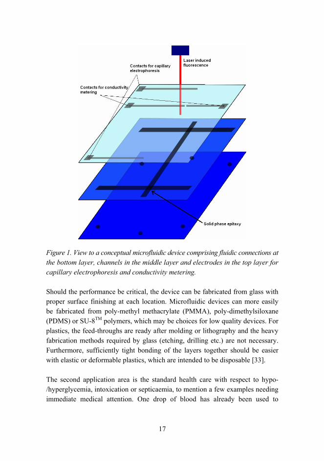
17
Figure 1. View to a conceptual microfluidic device comprising fluidic connections at the bottom layer, channels in the middle layer and electrodes in the top layer for capillary electrophoresis and conductivity metering.
Should the performance be critical, the device can be fabricated from glass with proper surface finishing at each location. Microfluidic devices can more easily be fabricated from poly-methyl methacrylate (PMMA), poly-dimethylsiloxane (PDMS) or SU-8TM polymers, which may be choices for low quality devices. For plastics, the feed-throughs are ready after molding or lithography and the heavy fabrication methods required by glass (etching, drilling etc.) are not necessary. Furthermore, sufficiently tight bonding of the layers together should be easier with elastic or deformable plastics, which are intended to be disposable [33].
The second application area is the standard health care with respect to hypo-/hyperglycemia, intoxication or septicaemia, to mention a few examples needing immediate medical attention. One drop of blood has already been used to

18
determine the blood glucose level for decades, but no commercial subcutaneous microdispenser for insuline exists [21]. It is possible to run this kind of device with a radio controller to simplify dosing procedure. With a portable microfluidic analyzer, it is also possible to determine certain chemicals and antigens in a matter of minutes and to promptly address the suitable cure according to the state of disease. For vaccinations or injection of drugs, the advantage of microfluidics lies in the design of array of miniature, thus painless, multifunctional needles [34, 35].
There is global interest for designing �lab-at-home� running analysis on substrates prefilled with suitable analytes and reagenses. It could save an enormous amount of money, if citizens were able to run tests on body fluids any time at home. Although a CD player or PC are easily accessible the concept has been mainly targeted for high-throughput systems. It obviously requires high level of reliability of the domestic diagnosis to alleviate doctors� work load.
Thirdly, the dietary industry is interested in finding contaminated food and drinks before they are delivered or at least before they are ingested. Here, microfluidics or gas sensors [36] are seldom the optimal choice until the sensitivity is improved to compete with conventional culturing plates. Process industry is still often accused of pollution or excess waste. With specific sensitive elements, microfluidics could be suitable for continuous sampling of waste water or fumes.
Environmental analytics deals with, for instance, toxins and microbes in urban sewage system, field drainage, ground water etc. Used fertilizers, pesticides and herbicides are traced from rural waste water and the concentration of cyanobacteria in swimming water is sometimes important to be determined. Here, the spot checks could be quickened dramatically with the aid of microfluidic portable indicators.
The high-throughput side is appreciated in clinical health care, where the DNA sequencing of viruses, microbes and cells are done. For these applications, there are seldom limits for the duration of the analysis of the analysis with the exception of epidemics and commercial race. On the other hand, stability, selectivity and sensitivity are often sought after. Finding specific interactions between different molecules and determining the affinity between them are

19
continuously recorded in e.g. immunoassays and drug screening. Drugs and other bioactive compounds are usually screened according to their ability to change the expression of specific genes or proteins. From the presence of certain proteins in blood, an imminent thrombus in an artery or vein, as well as a developing cancer, can be predicted. From the genome, the tendency towards heritable diseases or hypersensitiveness towards certain environmental factors can be evaluated. Portable microfluidic biosensors acting on saliva for drugs, doping and toxins enable fast assays on the field for forensics.
The high-throughput applications often require parallelisation of the assay and multiplication of specific DNA or RNA sequences. Presently, the most suitable technique is PCR, which is treated in sections 1.5 and 2.5.
1.3 Hydrophilic surfaces and capillary action
1.3.1 Definition
The design of a microfluidic device is strongly dependent on its surface properties. The division into hydrophobic and hydrophilic surfaces is the place to start at. The adhesion force of hydrophilic surfaces towards water molecules is stronger than the cohesion force between water molecules. Hydrophilicity can be attributed to surface energy of the substrate being low enough such that water molecules are attracted more by the surface than by water molecules themselves. Basically, water molecules have strong cohesion, i.e. high surface tension, which might limit the existence of hydrophilic surfaces [37].
However, this is not the situation in practice, since those surfaces which are rough or oxidized or exhibit polar molecules capable of hydrogen bonding can be highly hydrophilic. On these surfaces, the polar water molecules are attracted to almost any material and water fills any incorporating pore by capillary action. It has also been shown that hydrophilic surfaces are often covered by an adsorbed layer of water molecules [38].
Producing hydrophilic surface characteristics enables capillary action without external pumping or electro-osmosis [I, II]. Capillary action of an aqueous medium can only take place when surface of a capillary is hydrophilic so that a

20
droplet spreads on the surface (Fig. 2 left). The contact angle of the droplet is primarily used to define hydrophilicity of a given surface because it is very little dependent on the size of the droplet. With a contact angle smaller than about 90°, the surface can be considered as hydrophilic, as capillary action of an aqueous liquid is encouraged. The surface is then considered as wetting. A surface without hydrophilic and hydrophobic properties is here considered as neutral (Fig. 2 right). For this kind of a surface, the contact angle is as close to 90° as possible and it can be used for e.g. isobaric filling of sealed cavities (section 1.3.3).
Figure 2. Hydrophilic surface (left) and neutral surface (right) [II].
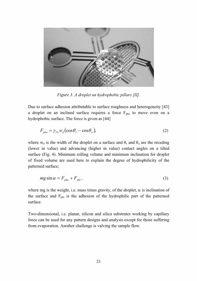
On the other hand, high coverage of hydrogen or fluorine on a surface or low roughness creates high surface energy, i.e. rejection of water molecules, thus making very hydrophobic surfaces possible [39, 40]. If the surface is hydrophobic, i.e. it has a high contact angle (> 90°), a droplet can be introduced even on top of pillars without losing its round shape or collapsing (Fig. 3).
Accordingly, the distinction between hydrophilic and hydrophobic surfaces lies in the contact angle between a sessile aqueous droplet and the surface of interest. Young's law for smooth, homogeneous and inert surfaces is usually written as [41]
,cos SLSVVL γγθγ −= (1)
where θ is the static contact angle and γ's are the surface tensions between solid (S), liquid (L) and vapour (V) phases. γSL can be measured as the critical surface tension, for which a liquid with surface tension equal to this value, experiences complete wetting [42].
21
Figure 3. A droplet on hydrophobic pillars [II].
Due to surface adhesion attributable to surface roughness and heterogeneity [43] a droplet on an inclined surface requires a force Fpho to move even on a hydrophobic surface. The force is given as [44]
( ),coscos ardVLpho wF θθγ −= (2)
where wd is the width of the droplet on a surface and θr and θa are the receding (lower in value) and advancing (higher in value) contact angles on a tilted surface (Fig. 4). Minimum rolling volume and minimum inclination for droplet of fixed volume are used here to explain the degree of hydrophilicity of the patterned surface;
phipho FFmg +=αsin , (3)
where mg is the weight, i.e. mass times gravity, of the droplet, α is inclination of the surface and Fphi is the adhesion of the hydrophilic part of the patterned surface.
Two-dimensional, i.e. planar, silicon and silica substrates working by capillary force can be used for any pattern designs and analysis except for those suffering from evaporation. Another challenge is valving the sample flow.

22
Figure 4. Interpretation of dynamic contact angles of a droplet on a tilted surface.
1.3.2 Valving and mixing
As described in reviews about microvalves [18] and micromixers [45, 46], many types of physical valving can be used to conduct precise valving and the designs based on agitation, turbulence or interlacing of flows can be used to conduct mixing. Triggered filling of predefined �self-feeding� volumes, i.e. volumes filling with capillary action is beneficial e.g. in cases when introduction of two fluids to be mixed is conducted separately. Here, triggering is aimed to enable simultaneous admission of the fluids to the mixing zone. The fluid menisci are retained within the pillars by surface energy and released to enter the mixing zone by heating. Thus, any significant uncertainty related to their amount or time separation is removed. In such cases the mixing is meant to occur primarily at a certain location and not necessarily in the whole volume of the fluids [II].
For some purposes, valves are not necessary, but instead the capillary flow in different channels can be controlled by pillars and the �break valve� can be crossed by heating the substrate. In section 2.3.4 the geometry of such a pillar gap mixer is illustrated. Pillars are generally fabricated for filtering or confinement purposes or their high surface area is utilized to enhance surface-
23
dependent performance of a device. They are also commercially used [47] to enhance the capillary action by decreasing aperture size for the advancing fluid front, but they are less essential for self-feeding when very hydrophilic uncovered surfaces or covered structures are concerned. As pillars are shrunk in size they approach the idea behind membranes, which can act as sites for confined chemical reactions, but also as valves [48�55]. The membranes with high porosity and swelling ability are often called hydrogels.
1.3.3 Filling by cooling
The filling of a microfluidic mixing chamber can also be triggered by negative hydrodynamic pressure i.e. a cooling gas volume [II]. The suction induces fluid penetration into cavity until pressure inside cavity equals the pressure of environment (Fig. 5). The round cavities (left) are only partially covered with a glass plate allowing initial dosage on the substrate in elevated temperature. When the temperature of the substrate is decreased, the pressure in the large cooling space is decreased.
Alternatively, for fixed pressure, a change in volume takes place. For gases, the (non-adiabatic) equation of state is expressed as
,0kTnpV = (4)
where p is the pressure, V the volume of interest, n0 the number of fluid molecules, k the Boltzmann�s constant and T the temperature. Hydrophilic surface encourages capillary action of fluid into sealed volume of gas until overpressure of the sealed gas equals surface energy gain due to hydrophilicity of capillary surfaces. Capillary force is here equated with pressure force as
00
cos (2 2 ) ,VLVw h wh P
V Vδγ θ
δ⋅ + =
+ (5)

24
where w and h are the width and the height of (rectangular) capillary, V0 the confined gas volume in ambient pressure, δV the change in the confined gas volume and P0 the ambient pressure.
Figure 5. The covered elliptic cavity fills with decreasing temperature of the trapped air from 42 °C (left) to 22 °C (right).
Furthermore, the surface tension of water decreases with increasing temperature. On a hydrophilic surface, this leads to further decreased contact angle at higher temperature and translates to enhanced capillary action. This is acting against the positive pressure generated in a sealed hydrophilic cavity.
In addition to triggering the fluid flow by the difference in temperature or surface morphology or by using physical valves, triggering can be achieved by a hydrophobic valve without moving parts. The usual way to use a hydrophobic valve is to have hydrodynamic back pressure operating slightly below and above the surface energy of the hydrophobic region made of a patterned hydrophobic coating [56�61].
Trapped air
Moving meniscus
Feeding droplet

25
1.4 Fabrication of microfluidic devices
1.4.1 Silica vs. glass
Although there exists considerable experience to fabricate silicon-based devices, silica and glass are considered superior to silicon when optical transparency, low electrical conductance and biocompatibility are required. Silica and glass also overcome many limitations of polymers because of their low auto-fluorescence, mechanical durability, reusability and smooth surfaces. Therefore, while silicon serves as the work horse also in this thesis, the fabrication of glass has been developed to a new level [III, IV, V]. Polymers are only considered with SU-8 epoxy polymer (see section 2.2.3) and a plasma polymer film (see section 2.4).
There are different qualities of silica readily available for facilities capable of microfabrication processes. Silica in its purest amorphous form is fused silica, which is delivered as wafers beginning from 100 µm thickness or thermal silicon dioxide, which is grown on silicon at high temperatures (> 900 °C) in an atmosphere containing oxygen. In contrast to crystalline quartz, the amorphous silica tolerates high temperatures and stress induced by foreign layers on the wafer. Silica can be grown very close to its stoichiometric form (SiO2) also in lower temperatures (< 500 °C), but usually the resulting layers grown in chemical vapour deposition (CVD) chambers tend to be rich in silicon. There is also unintended nitrogen and hydrogen present in the layer, which induce internal stress in the silica layer. The contamination is significant in plasma enhanced (PE) CVD, where the temperature is 120�400 °C. However, by tuning mass flows of deposition precursors SiH4, N2O, N2, NH3 and by adding Ar to the plasma, refractive index of the deposited silicon oxinitride SiOxNy layer can be adjusted between 1.45 and 2.4 (at He-Ne laser wavelength 633 nm), and stress of the deposited layer can be chosen between -600 to 600 MPa [62].
Intentional contamination i.e. doping of silica with e.g. boron, sodium, potassium or lead has widely been used for producing the different grades of glasses for different purposes. These glasses include PyrexTM, which has been matched to the thermal expansion of silicon for bonding purposes and which has been studied in this thesis.

26
1.4.2 Microfabrication of silicon and glass
Microfluidic structures are usually fabricated with microfabrication methods. The primary part of the fabrication is forming the required channels and cavities. The choice between the fabrication methods depends on the number and shape of the required features and they apply to both silicon and glass. Chemical etching processes [63, 64] for glass or gaseous etching processes such as XeF2 for silicon [65] and HF vapour for silica [66] are used when isotropic etch characteristics are allowed. The chemical etching may have very high etching selectivity, i.e. the ratio of the etch rates of the material to be etched to the masking material, so that the mask will not essentially be consumed at all. The disadvantages of the chemical etching of glass include the isotropic etch behaviour, i.e. the etch rate is similar in every direction in the material to be etched, and its high requirement on the integrity and the adhesion of the etch mask.
Ion beam etching, also known as ion milling, utilizes noble gas ions [67]. It is pure physical sputtering without chemical reactions and it can be used for etching materials which can not easily be etched chemically. It suffers from low etch rate and from low etching selectivity to any masking material. Plasma jet is also a commercialized technique [68]. By using a suitable mask, the plasma jet can be defocused to etch a larger area of few square centimetres and to yield high aspect ratios. In powder blasting i.e. abrasive jet machining [69, 70], hard particles are blown to the surface with high velocity causing erosion. By using an elastic mask which is not eroded by the silicon carbide or sapphire particles, it is possible to form moderate aspect ratios in glass and furthermore, the angle of attack can be adjusted to yield non-vertical features.
Localised anisotropic structuring of silica can also be accomplished without masking. In addition to the mentioned powder blasting, ion milling and plasma jet, drilling or laser ablation [71, 72] can be used. Drilling is the most efficient and user-friendly method for low number of round holes with low aspect ratio. Laser ablation which is also used for producing distinct atoms, molecules or ions for elemental analysis of solid materials, requires process optimisation for each glass composition and thickness. The rest of the techniques suffer from poor resolution, low aspect ratio and non-vertical profiles when used without mask. If mechanical stress, possible fractures and drilling waste are to be avoided, plasma jet may be the choice. As in ion beam milling utilizing high energy ions without
27
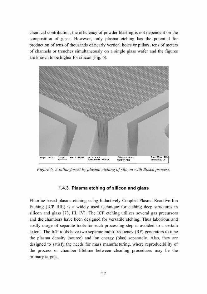
chemical contribution, the efficiency of powder blasting is not dependent on the composition of glass. However, only plasma etching has the potential for production of tens of thousands of nearly vertical holes or pillars, tens of meters of channels or trenches simultaneously on a single glass wafer and the figures are known to be higher for silicon (Fig. 6).
Figure 6. A pillar forest by plasma etching of silicon with Bosch process.
1.4.3 Plasma etching of silicon and glass
Fluorine-based plasma etching using Inductively Coupled Plasma Reactive Ion Etching (ICP RIE) is a widely used technique for etching deep structures in silicon and glass [73, III, IV]. The ICP etching utilizes several gas precursors and the chambers have been designed for versatile etching. Thus laborious and costly usage of separate tools for each processing step is avoided to a certain extent. The ICP tools have two separate radio frequency (RF) generators to tune the plasma density (source) and ion energy (bias) separately. Also, they are designed to satisfy the needs for mass manufacturing, where reproducibility of the process or chamber lifetime between cleaning procedures may be the primary targets.

28
Plasma etching allows exploitation of both chemical and physical processes to remove solid material locally. In terms of etch rate, all methods; chemical etching, physical ion etching and plasma etching fall in the same range (0,5�5 µm/min).
Silicon can be etched with a continuous process without switching the etching (SF6) and the passivation (C4F8) gases, just as glass is etched. Etching of silicon is based on flux of fluorine radicals onto the surface, while etching of glass requires high ion energies and preferably CF2 radicals. The yield of fluorine radicals is high with SF6 and CF4 gases. On the other hand, C4F8 readily dissociates into CF2 radicals, which etch glass but also deposits as a passivating polymer on both silicon and glass. Due to the requirement of penetrating the polymer, high ion energies are needed in glass etching.
The contribution of radicals is clearly visible when etch rates of alumina (Al2O3) or titania (TiO2) and silica are compared with C4F8 or CHF3 gas precursors [VI]. Al2O3 and TiO2 show almost a linear dependence between the bias voltage (ion energy) and etch rate, while silica experiences a knee when approaching a saturation etch rate at moderate bias voltages. At the knee, the etching of silica is changed from ion-constrained to radical-constrained.
Furthermore, the optimal process pressure is lower for glass etching than for silicon because the mean free path of ions, radicals and etch products is then increased to allow their better penetration and escape from high aspect ratio structures. However, silicon is usually etched with the switched Bosch process or a cryo process, which both utilize enhanced passivation of sidewalls of the etched features to reach high aspect ratios and high etch rate. The Bosch process is further described in section 2.1.
The different requirements for etching silicon and glass often require different process chambers and gas chemistries. For this thesis, STS ASETM (Advanced Silicon Etcher) and STS AOETM (Advanced Oxide Etcher) equipment were used for etching silicon and glass, respectively. AOE utilizes planar coil instead of helical as the source of plasma. Large chamber, turbo pump and RF generators in AOE as well as the mechanical wafer clamping and high chamber temperature (100�200 °C) facilitate the etching of glass.

29
The advantageous properties of plasma etching have been used in all fields of microfabrication, i.e. microelectronics [74], microelectromechanical systems (MEMS) [75�77] and microphotonics [78]. The plasma etching is especially advantageous in microfluidics because the hydrophilicity of the etched surfaces can be adjusted with O2 plasma exposure after etching [I, II].
Like all other techniques, plasma etching requires optimisation of the etching parameters and a suitable choice of masking material for each application. For instance, the etching parameters and the mask requirements are different depending on the depth of the etching. In shallow etching (< 5 µm), high uniformity and highly vertical side wall profiles are often required. Also, optical waveguides and mirrors and detection systems may have stringent requirements on surface roughness as well as on abruptness of the etched area [79�82].
High aspect ratios, > 3:1 for glass and > 20:1 for silicon, may be required in deep etching for microfluidics, as well as in photonic crystals, sensor surfaces and filters or whenever the packing density is to be maximised.
In addition to deep etching, in manufacturing of integrated electronic circuitry, the etching selectivity to the mask or to the underlying material may have to be maximised. The highest possible etching selectivity is usually limited by the physical character of the etching method, but it may be enhanced by an additional material-selective protection from the plasma, such as when a polymerizing plasma etching is used. For a purely physical etching, all materials are etched essentially with the same rate, thus reaching a high etching selectivity against any masking material becomes impossible. In deep structures, a high etch rate is obviously preferred.
It was mentioned that silica and glass can be etched with plasma formed from C4F8 precursor, but also other precursors such as CHF3, CF4 and SF6 can be used [83�93]. For etching glass with a silicon mask, SF6 or CF4 can not be used because of the high fluorine radical yield leading to fast chemical etching of silicon. Instead, chemistries involving CFx radicals and ions are used, particularly those generating CF2 radicals and ions, because they are efficient in oxide etching, but not in silicon etching. The chemistries yielding the most CF2 utilise C4F8 and CHF3 precursors.

30
Additional inert atoms can be used to further transform the produced fluorine radicals and ions into CFx (and possibly HF). Gases like H2, Ar and He are also used to improve stability of the plasma and etch selectivity [94].
1.4.4 Plasma etching of silicon and glass, challenges
For etching low sputter yield materials i.e. those usually amorphous materials which have strong chemical bonds like glasses, the physical character of etching, i.e. high energy ions, must be utilized. Compared to deep silicon etching, the plasma etching of glass has suffered from limitations in achievable depth, aspect ratio and etching selectivity [V, VI]. The pulsed Bosch process or cryo processes used to obtain high aspect ratio and etching selectivity in silicon etching can not be used for oxides.
The anisotropic character of the plasma etching overcomes many limitations introduced by isotropic wet etching techniques (A in Fig. 7), but benefits from the high chemical etch rate and etching selectivity. However, the faceting of edges of mask causes the sidewalls to develop non-vertical in plasma etching of glass (B in Fig. 7). Faceting does not influence on the etched feature with low aspect ratios and when only a small portion of the mask is eroded during etching.
Due to the anisotropic nature of the ion bombardment, some of the problems which may occur during the etching of silicon are less significant for glass. Underetching i.e. etching under the mask as in isotropic chemical etching (C in Fig. 7) and notching i.e. the lateral etching next to an etch stop layer (D in Fig. 7) are sometimes encountered in silicon etching but not in glass etching. Loading effects, depending on the local proportion of the area to be etched to the total area and leading to non-uniform etch rate, are also less significant on glass. This is because the etch rate of glass is not limited by the flux of neutral radicals, which is mainly dependent on the flow of the etching gas and source power, but by the ion flux to the surface. The etch rate uniformity over a wafer and verticality of the walls of the etched features are usually good in glass etching.
One of the challenges in glass etching with plasma is micromasking (E in Fig. 7), which happens when small particles of the mask sputter off and land on the area to be etched. It is not such a problem for purely chemical or purely physical etching, since they are isotropic or non-selective, respectively. Micromasking is

31
not a significant problem in etching glass with silicon mask, as silicon has a relatively low etching selectivity to glass. However, if both the high chemical etching selectivity and the anisotropic physical etch are required, sputtered particles of the mask material or of non-volatile etch products may shadow significant areas of the material to be etched. Plasma etching suffers from the non-volatile fluorides produced in plasma etching sodium, potassium and lead oxides with fluorine-based gases. Thus, etch performance and optimal etching conditions may differ significantly for different types of glasses. Only precursors containing fluorine has been observed effective in plasma etching glass, while also chlorine can be used for silicon.
Figure 7. The different etching characteristics: a) isotropic (wet) etching, b) plasma etching with mask facets, c) directional plasma etching with isotropic character (underetching), d) notching on the etch stop layer and e) micromasking.
One major challenge which glass etching shares with silicon etching is RIE lag [74], which is a consequence of aspect ratio dependent etch rate (ARDE). With ARDE, small features are etched with a lower rate than wider features because they develop higher aspect ratio. In fact, compared to Bosch (Fig. 6) or cryo silicon etching processes, ARDE leading to non-uniform etch depth is more severe in glass etching with a continuous process. This is due to the difficulty for the etching ions and radicals to reach the bottom of a high aspect ratio feature with high enough energy.
For the standard processes of etching glass with C4F8, lots of polymer is formed. The polymer deposition occurs preferably on silicon protecting it and allowing a good etching selectivity with a silicon mask. The ion energies are set high in oxide

32
etching for the ions to penetrate the (thinner) polymer layer on the oxide. The formation and deposition rates of the polymer depend on all parameters of the process, but mainly on pressure, the C4F8 flow rate and both source and bias powers.
Another complication, which arises during deep etching of glass stems from the presence of oxides other than silica, which produce non-volatile fluorides. These fluorides redeposit in the etching equipment, if they leave the etched area at all. As well, they can cause micromasking (E in Fig. 7).
In addition to the micromasking phenomena, there are also substantial challenges in faceting, which can be understood as lateral etch rate of the edge of the mask (B in Fig. 7) and in high surface roughness due to high ion energies.
Deep structures with nearly vertical side walls have been achieved on silica and borosilicate, but they either require laborious masking procedure and a special chamber or the achieved depth is severely limited [78�80]. The use of shadow mask without any practical depth limitations has been reported for etching silicon [95] and glass [87], but complex pre-processing, i.e. anodic bonding and thinning of the silicon shadow mask wafer has been required. The achieved aspect ratio has been limited and, furthermore, the reported masks can only be used once. When the plasma etching process is optimized, through holes with moderate aspect ratio in silica and PyrexTM wafers can be realized and the non-bonded silicon shadow mask can be reused [III].
1.5 Polymerase chain reaction
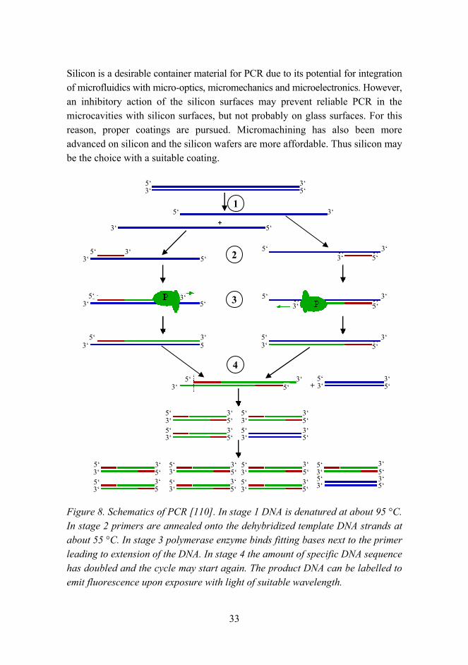
1.5.1 General
PCR (Fig. 8) is a widely used technique to multiply low concentrations of specific real life DNA samples for convenient detection and analysis. The selectively amplified DNA product from i.e. genomic DNA is quantified by dyes attaching to double-stranded DNA only (e.g. SYBR Green) or releasing upon production of the specific DNA sequence (e.g. TaqMan). There is a lot of activity in transferring the PCR into microchip format [96�109]. The author has also fabricated microchips for PCR as well as for CE, which have no novel properties explored in this work.
33
Silicon is a desirable container material for PCR due to its potential for integration of microfluidics with micro-optics, micromechanics and microelectronics. However, an inhibitory action of the silicon surfaces may prevent reliable PCR in the microcavities with silicon surfaces, but not probably on glass surfaces. For this reason, proper coatings are pursued. Micromachining has also been more advanced on silicon and the silicon wafers are more affordable. Thus silicon may be the choice with a suitable coating.
Figure 8. Schematics of PCR [110]. In stage 1 DNA is denatured at about 95 °C. In stage 2 primers are annealed onto the dehybridized template DNA strands at about 55 °C. In stage 3 polymerase enzyme binds fitting bases next to the primer leading to extension of the DNA. In stage 4 the amount of specific DNA sequence has doubled and the cycle may start again. The product DNA can be labelled to emit fluorescence upon exposure with light of suitable wavelength.
5� 3�
5�
5�
5�
5�
5�
5�
5� 5�
5�
5�
5�
5� 5� 5�5� 5�
5� 5
5� 5�
5�5�
5�5�
5�5�
5�
5�
5�
5� 5�
5�
5� 5�
5�5�
5� 5�
5�
5�
5�
5
3�
3�
3�
3� 3�
5�
3�3�3�
3� 3�
3�
3� 3� 3�
3�
3� 3�
3� 3�3�
3�
3�
3� 3�
3� 3�
3� 3�
3� 3�
3�
3� 3�
3�
3�
3�
3�
4
3�
3�
3�
3�
+
3�3�
3
2
1
34
1.5.2 Failure studies of PCR
The surfaces of the material of the cavity or the container in which the PCR is done are of primary importance. Many materials have been considered as unreliable in terms of whether they can reproducibly support PCR, while some polymers such as polyethylene and polypropylene and silica glass are widely used as PCR container materials. Also the possibility of using polymers other than polyethylene or polypropylene as PCR containers have been studied [103, 104].
The ratio of an inhibitory surface area to the volume of the PCR mixture (surface to volume ratio, SVR) generally displays a clear positive correlation to inhibition efficiency. For example, silicon and silicon nitride (SiNx or Si3N4) have shown severe inhibitory action towards PCR through surface immobilization or catalysis. To study the inhibition of PCR on different materials, PCR microchips have been fabricated [103, 111�121]. Silanization and polymer coatings have also been studied on powdered silicon immersed into the PCR mix [111, 113], but uniform deposition or growth of silicon oxides thicker than native oxide or deposition of silicon nitride is difficult on powder. The evaluation of PCR inhibition has been based mainly on post-PCR gel electrophoresis of microchip PCR products, but also real-time analysis has been performed on silicon microchips [119], on silicon powder [120] and now also on small pieces of silicon coated with different silicon oxides [VIII].
There exist also dynamic coatings, such as bovine serum albumine (BSA) and poly-vinyl pyrrolidone (PVP), which are added to the PCR mixture. Their counter-inhibitory roles have earlier been confirmed with respect to PCR [118, 122].
The real-time analysis is generally more informative than a post-PCR analysis of the amplification results. First, the real-time method suppresses the possibility of cross-contamination between the reactions. Secondly, the fluorescence levels of DNA amplification in each reaction can be quantitatively monitored throughout the PCR leading to deeper insight into the possible inhibition mechanisms. Thirdly, the amplification results of 96-plates are obtained from a large amount of reactions simultaneously.
In earlier studies it has been observed that native silicon adsorbs TaqManTM real-time PCR label [120], but no studies have been performed with SYBR GreenTM
35
dye. Also, in earlier studies no attention has been paid on the starting template amount, even though it can offer more information about the inhibition effects.
Microfluidic chips running PCR or other chemical or biological assay require detection capabilities to obtain the status of �total analysis system�. One large section of detection methods is based on specific light emission of molecules, to be discussed in the next chapter.
1.6 Evanescent wave fluorescence analysis
1.6.1 General
One important group of methods for detecting the presence of specific molecules in a microfluidic chip are optical detection techniques. The other main branches are electrical, thermal and mechanical detection systems.
The domain of optical detection methods is generally divided into methods based on emission, absorption or change in refractive index. They can also be categorized as non-resolved and resolved detection methods. The former encompasses e.g. absorption of a certain wavelength corresponding to an amount of species to be detected or a change in refractive index induced by an immobilised mass in a regime of interest. The latter utilises spectral resolving (i.e. filtering, fluorescence, two-photon excitation), chemical resolving (i.e. intermediate specific molecular tags in immunoassays), spatial resolving (i.e. evanescent field, confocal microscopy) or temporal resolving. A combination of resolving techniques can be utilised for enhanced sensitivity or versatility.
The majority of the research on optical detection of nucleic acid molecules is focused on utilising an evanescent field, where waveguiding structures utilise total internal reflection (TIR) for confined propagation of an electromagnetic (EM) field. This method allows the EM field to reach a short distance outside the waveguide core, leading to fluorescence i.e. excitation and de-exitation of electronic levels of molecules in proximity of the surface of the waveguide core. On a microchip, it is possible to use a surface sensitive laser beam for evanescent wave detection after the beam is coupled into a waveguide [VIII, 123�135] (Fig. 9), as in surface plasmon resonance (SPR) reported 25 years ago [30].

36
From a purely detection point of view, advanced avalanche photodiodes enable detecting single photons [136], but then parallelism is compromised and instrumentation becomes demanding and costly. With a CCD it is possible to monitor simultaneously multiple small fluorescent spots with high sensitivity and low cost for instrumentation [VIII].
Figure 9. Schematics of an incident laser beam exciting a propagating field in the waveguide core and the evanescent field outside the core [VIII].
1.6.2 Characterisation of grating coupling and evanescent field
Grating coupling of the laser beam into a waveguide is one of the coupling methods. Other methods are end-coupling and prism coupling. According to the well-known grating theory, to achieve a guided propagation of grating-coupled light in a waveguide, the following conditions have to be satisfied. First, the grating only produces diffracted orders such that [137]
,Λ/2 + = κπβ mneffcos (6)
where β is the incidence angle as measured from the grating plane and from the direction of propagation, neff denotes the effective refractive index of a
37
propagating mode, m is diffraction order of the grating, κ is wave vector of incident beam in vacuum and Λ is the period of the grating. Secondly, the waveguide was aimed at two-mode operation, i.e. supporting propagation of only the 0th and the 1st order waveguide modes:
2,,1, effCSeff nnn >> . (7)
Here subscripts 1 and 2 refer to the order of TE (transverse electric, electric field vector of light waves parallel to the grooves of grating) and TM (transverse magnetic, electric field vector of light waves perpendicular to the grooves of grating) modes, S to substrate and C to cover. The cut-off condition for the 2nd order waveguide modes [138] is
2
02,
2
2 ⎟⎟⎠
⎞⎜⎜⎝
⎛>−
FCSF t
nnλ
, (8)
where the subscript F refers to the waveguide film, t to thickness of the film, and λ0 to the wavelength of excitation beam in vacuum (and air). The theoretical maximum of diffraction efficiency for gaussian beam [139] has been considered in the context of practical gratings [VIII].
The penetration depth d of an evanescent field is generally defined as 1/e length of field intensity penetrating into the surroundings of the guiding core of the waveguide. This depth is calculated from
./(4 2,
2220 CSeff nnd − =)πλ (9)
The grating coupling method has been characterized in this thesis as the last part of the �total analysis system�, because the evanescent field method can be utilized for monitoring e.g. PCR.
38
2. Experiments
2.1 Plasma etching of silicon
The through etched silicon shadow masks (see sections 2.2.2 and 2.4.2) and the silicon microchips used in this work [I�IV, 73, 108] were fabricated using the Bosch process in STS ASE� ICP RIE equipment. The 525±15 and 400±10 µm standard silicon wafers were patterned with 2 µm PECVD, low pressure (LP) CVD or thermal silicon dioxide mask and subsequently etched in ASE to form through-holes of different size (100�2000 µm) for experiments on droplet manipulation (see section 2.4) and nozzle structures (see section 2.2.4) or 400 µm deep channel matrices for capillary action and capillary electrophoresis (see section 2.3) experiments. The oxide masks were patterned in standard RIE tools after standard photolithography.
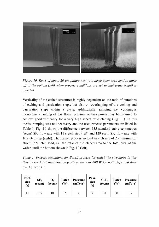
When silicon is etched with the Bosch process, optimization of the process is required for each layout design and the target etch depth. In this thesis aspect ratios of about 20:1 and 400 µm etch depth were necessary (Fig. 6). In some chips, a few rows of 25 µm pillars were designed next to a large open area (Fig. 10 left). The presence of such pillars is an important factor when finding optimal process conditions for the deep silicon etch. Surface finish was not important due to subsequent thermal oxidation of the etched structures, except that �grass� had to be avoided (Fig. 10 right). Grass is a form of micromasking generated by excess passivation polymer or redeposition of mask material.
The Bosch process relies on the fact that the passivation polymer is first sputtered off at horizontal surfaces by fluorine radicals due to directional ion bombardment from above the substrate. After the penetration of the polymer film, the fluorine radicals etch silicon almost isotropically and to sustain the vertical walls the etching has to be stopped after a few seconds. Even though the fluorine radicals consume the polymer covering the horizontal silicon dioxide mask, it is very little etched by the radicals and by the low ion energies which are still sufficient to aid in etching silicon.
39
Figure 10. Rows of about 20 µm pillars next to a large open area tend to taper off at the bottom (left) when process conditions are set so that grass (right) is avoided.
Verticality of the etched structures is highly dependent on the ratio of durations of etching and passivation steps, but also on overlapping of the etching and passivation steps within a cycle. Additionally, ramping, i.e. continuous monotonic changing of gas flows, pressure or bias power may be required to achieve good verticality for a very high aspect ratio etching (Fig. 11). In this thesis, ramping was not necessary and the used process parameters are listed in Table 1. Fig. 10 shows the difference between 135 standard cubic centimetres (sccm) SF6 flow rate with 11 s etch step (left) and 129 sccm SF6 flow rate with 10 s etch step (right). The former process yielded an etch rate of 2.9 µm/min for about 15 % etch load, i.e. the ratio of the etched area to the total area of the wafer, until the bottom shown in Fig. 10 (left).
Table 1. Process conditions for Bosch process for which the structures in this thesis were fabricated. Source (coil) power was 600 W for both steps and their overlap was 1 s.
Etch step (s)
SF6 (sccm)
O2 (sccm)
Platen(W)
Pressure(mTorr)
Pass. step (s)
C4F8 (sccm)
Platen (W)
Pressure (mTorr)
11 135 10 15 30 7 98 0 17

40
Figure 11. Very high aspect ratio etching of silicon with ramping of gas flows and bias power (left) is not necessary with standard microchips (right).
Due to the cyclic nature of Bosch process, an undulation is formed to the etched sidewall during each cycle (Fig. 12). These undulations have amplitude of about 100 nm and period of about 1 µm and they can have a significant role in surface roughness in microfluidic but also in other applications [78].
Figure 12. Bosch process induces lateral undulation on the etched side walls.

41
The fabrication of narrow pillars is demanding because the requirement for the penetration of the etching radicals between the pillars is different in the beginning and in the end of the etching. One might think that it would be clever to tune the process according to the hardest requirements; the end of the etching. By doing so the etching selectivity and verticality of the pillar walls are deteriorated. When pillars were required to stand next to a large open area the sidewall passivation became excessive between the pillars. When passivation was reduced, it ran out quickly on the walls of the large well due to lateral flux of scattered radicals. When etching was performed deeper than about 350 µm, increasing the SF6 flow to about 140 sccm and increasing the bias (platen) power to 20 W were observed beneficial in avoiding grass and to make the etching more anisotropic for the pillars to stand. The etching selectivity decreases significantly with increasing bias power so the change was made for the last 15 % of the etch depth. The process in Table 1 was optimized so that the 25 µm pillars were standing next to a large well while still well differentiated from each other. In round thru-holes, 300 µm holes in the oxide mask ended up as 300 µm features at the bottom of the wafer. Here, larger features had slightly negative side wall profiles and smaller features had positive (< 90°) side wall profiles.
As fluorine and carbon residues from etch (SF6) and passivation (C4F8) gases can be mostly removed after the plasma etching of silicon by O2 treatment, the hydrophobic character of the etched surfaces can be modified. In this thesis this is shown to be useful for microfluidic substrates [I, II].
2.2 Plasma etching of glass
2.2.1 General
The silica and PyrexTM features in this thesis were fabricated with STS AOETM ICP RIE tool [III, IV], which is equipped with mechanical clamping to allow holding dielectric and bowed wafers as well as wafer stacks on the platen in place. Also the Si3N4 gratings for evanescent field detection (section 2.6) were fabricated in AOE [VIII].
In the search for optimal process conditions for very deep etching of silica and PyrexTM wafers, as vertical wall profiles as possible with a reasonable aspect

42
ratio have been emphasized. Also low surface roughness and low etch rate of mask both in the lateral and vertical direction have been appreciated. The lateral etch rate of the mask was measured in the upper corners (on the side of the plasma) of the thru-holes concerning the silicon shadow masks.
While the bottom of the silica etched with C4F8 plasma can be even smoother than that of silicon (see section 2.3.2), silica walls have vertical striations and facets (Fig. 13). Both phenomena are due to the required high bias energy for ion bombardment during silica etching, inducing faster erosion on the edges of the mask, as compared to overall etch rate of the mask. With a metal or photoresist masks the situation is generally similar. As the mask edges have original roughness after its patterning and the mask is not eroded evenly during silica etching, the vertical striations are formed. These striations induce roughness of magnitude of 100 nm, but they are diminished in upper region of etched structure due to off-vertical facets.
Figure 13. Facets on the edge of the mask and vertical striations on the wall of the etched structure [III].
If depths less than about 150 µm and low aspect ratios are satisfactory, thin film masks (see section 2.2.5) such as as-deposited amorphous silicon (a-Si) suffice. The only problem may be the need for very thick films (> 7 µm), which may lead to cracking of the mask due to internal or heat-induced stress or to excessive maintenance of the masking equipment.
43
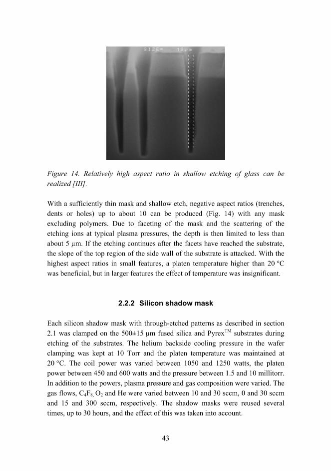
Figure 14. Relatively high aspect ratio in shallow etching of glass can be realized [III].
With a sufficiently thin mask and shallow etch, negative aspect ratios (trenches, dents or holes) up to about 10 can be produced (Fig. 14) with any mask excluding polymers. Due to faceting of the mask and the scattering of the etching ions at typical plasma pressures, the depth is then limited to less than about 5 µm. If the etching continues after the facets have reached the substrate, the slope of the top region of the side wall of the substrate is attacked. With the highest aspect ratios in small features, a platen temperature higher than 20 °C was beneficial, but in larger features the effect of temperature was insignificant.
2.2.2 Silicon shadow mask
Each silicon shadow mask with through-etched patterns as described in section 2.1 was clamped on the 500±15 µm fused silica and PyrexTM substrates during etching of the substrates. The helium backside cooling pressure in the wafer clamping was kept at 10 Torr and the platen temperature was maintained at 20 °C. The coil power was varied between 1050 and 1250 watts, the platen power between 450 and 600 watts and the pressure between 1.5 and 10 millitorr. In addition to the powers, plasma pressure and gas composition were varied. The gas flows, C4F8, O2 and He were varied between 10 and 30 sccm, 0 and 30 sccm and 15 and 300 sccm, respectively. The shadow masks were reused several times, up to 30 hours, and the effect of this was taken into account.
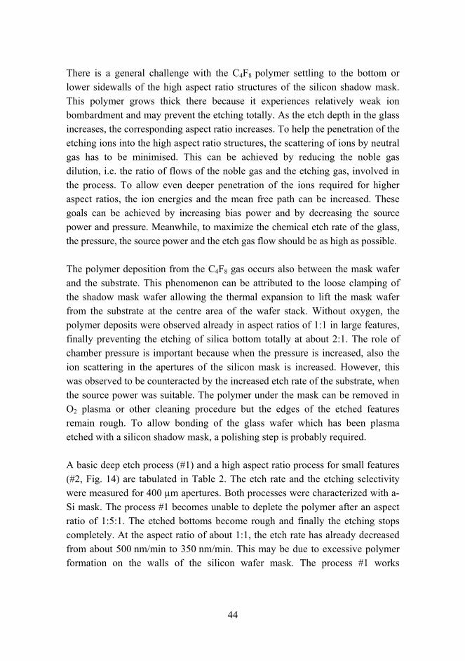
44
There is a general challenge with the C4F8 polymer settling to the bottom or lower sidewalls of the high aspect ratio structures of the silicon shadow mask. This polymer grows thick there because it experiences relatively weak ion bombardment and may prevent the etching totally. As the etch depth in the glass increases, the corresponding aspect ratio increases. To help the penetration of the etching ions into the high aspect ratio structures, the scattering of ions by neutral gas has to be minimised. This can be achieved by reducing the noble gas dilution, i.e. the ratio of flows of the noble gas and the etching gas, involved in the process. To allow even deeper penetration of the ions required for higher aspect ratios, the ion energies and the mean free path can be increased. These goals can be achieved by increasing bias power and by decreasing the source power and pressure. Meanwhile, to maximize the chemical etch rate of the glass, the pressure, the source power and the etch gas flow should be as high as possible.
The polymer deposition from the C4F8 gas occurs also between the mask wafer and the substrate. This phenomenon can be attributed to the loose clamping of the shadow mask wafer allowing the thermal expansion to lift the mask wafer from the substrate at the centre area of the wafer stack. Without oxygen, the polymer deposits were observed already in aspect ratios of 1:1 in large features, finally preventing the etching of silica bottom totally at about 2:1. The role of chamber pressure is important because when the pressure is increased, also the ion scattering in the apertures of the silicon mask is increased. However, this was observed to be counteracted by the increased etch rate of the substrate, when the source power was suitable. The polymer under the mask can be removed in O2 plasma or other cleaning procedure but the edges of the etched features remain rough. To allow bonding of the glass wafer which has been plasma etched with a silicon shadow mask, a polishing step is probably required.
A basic deep etch process (#1) and a high aspect ratio process for small features (#2, Fig. 14) are tabulated in Table 2. The etch rate and the etching selectivity were measured for 400 µm apertures. Both processes were characterized with a-Si mask. The process #1 becomes unable to deplete the polymer after an aspect ratio of 1:5:1. The etched bottoms become rough and finally the etching stops completely. At the aspect ratio of about 1:1, the etch rate has already decreased from about 500 nm/min to 350 nm/min. This may be due to excessive polymer formation on the walls of the silicon wafer mask. The process #1 works

45
satisfactorily for aspect ratios up to 4:1 in small (< 10 µm) features possibly due to the mean free path of the plasma exceeding greatly the depth of the feature.
The main difference between process #2 and process #1 is the lower He flow. The role of the noble gas is mostly to allow higher etching selectivity through decreasing bias. It also leads to lower etch rate of glass and to less anisotropic etching characteristics. The etch rate of the process #2 is about 660 nm/min in small features until about aspect ratio of 1.5:1. In large features, the process #2 is unable to remove the polymer above aspect ratio of 2:1 and the polymer deposition between the mask and the substrate is strong.
The process #3 allows slightly increased aspect ratio in large features by the addition of oxygen. Increasing the partial pressure of oxygen causes enhanced scattering of accelerating ions just as increasing the partial pressure of the noble gas does. This leads to a decreased etch rate of glass. On the contrary to the noble gas, adding oxygen also leads to increased etch rate of silicon. The polymer shielding the horizontal silicon surface is efficiently oxidized, i.e. removed, leading to a decreased vertical etching selectivity. Also, the polymer shielding laterally the silicon apertures is constantly removed, causing the lateral etch rate of the mask to increase. One more possibility to the increased etch rate of silicon is an increased fluorine radical concentration due to presence of oxygen.
Lateral etch rate is of the same origin as faceting and it has here been measured from the top of the mask. It can clearly be seen to affect first on the aspect ratio of the feature in the mask (Fig. 15) and once the facet reaches the substrate, then also the top of the etched feature is attacked. The initial mask has experienced about 115 µm erosion laterally and 175 µm erosion vertically after 20 hours of etching. The bottom of the mask has not yet eroded laterally, but if etching is continued with the mask and the process, the side walls of the substrate begin to tilt off the vertical.
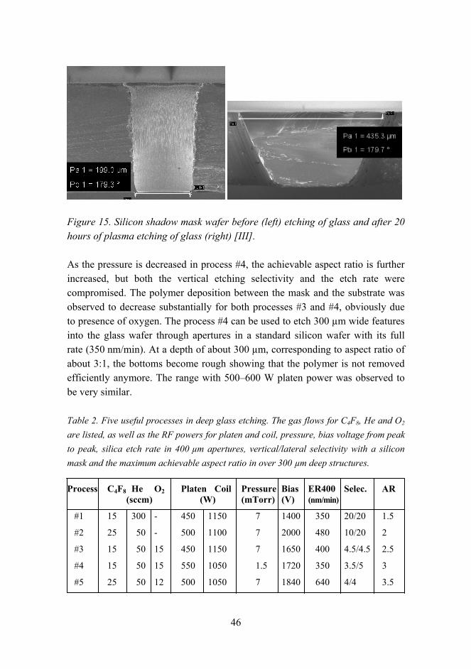
46
Figure 15. Silicon shadow mask wafer before (left) etching of glass and after 20 hours of plasma etching of glass (right) [III].
As the pressure is decreased in process #4, the achievable aspect ratio is further increased, but both the vertical etching selectivity and the etch rate were compromised. The polymer deposition between the mask and the substrate was observed to decrease substantially for both processes #3 and #4, obviously due to presence of oxygen. The process #4 can be used to etch 300 µm wide features into the glass wafer through apertures in a standard silicon wafer with its full rate (350 nm/min). At a depth of about 300 µm, corresponding to aspect ratio of about 3:1, the bottoms become rough showing that the polymer is not removed efficiently anymore. The range with 500�600 W platen power was observed to be very similar.
Table 2. Five useful processes in deep glass etching. The gas flows for C4F8, He and O2 are listed, as well as the RF powers for platen and coil, pressure, bias voltage from peak to peak, silica etch rate in 400 µm apertures, vertical/lateral selectivity with a silicon mask and the maximum achievable aspect ratio in over 300 µm deep structures.
Process C4F8 He O2 Platen Coil Pressure Bias ER400 Selec. AR (sccm) (W) (mTorr) (V) (nm/min)
#1 15 300 - 450 1150 7 1400 350 20/20 1.5
#2 25 50 - 500 1100 7 2000 480 10/20 2
#3 15 50 15 450 1150 7 1650 400 4.5/4.5 2.5
#4 15 50 15 550 1050 1.5 1720 350 3.5/5 3
#5 25 50 12 500 1050 7 1840 640 4/4 3.5
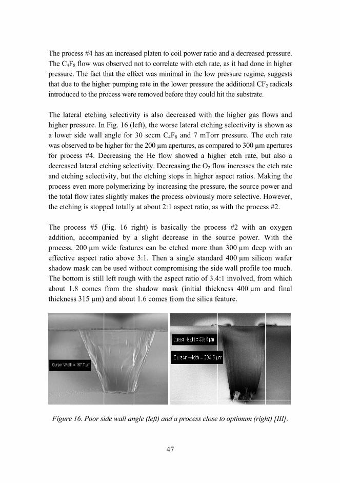
47
The process #4 has an increased platen to coil power ratio and a decreased pressure. The C4F8 flow was observed not to correlate with etch rate, as it had done in higher pressure. The fact that the effect was minimal in the low pressure regime, suggests that due to the higher pumping rate in the lower pressure the additional CF2 radicals introduced to the process were removed before they could hit the substrate.
The lateral etching selectivity is also decreased with the higher gas flows and higher pressure. In Fig. 16 (left), the worse lateral etching selectivity is shown as a lower side wall angle for 30 sccm C4F8 and 7 mTorr pressure. The etch rate was observed to be higher for the 200 µm apertures, as compared to 300 µm apertures for process #4. Decreasing the He flow showed a higher etch rate, but also a decreased lateral etching selectivity. Decreasing the O2 flow increases the etch rate and etching selectivity, but the etching stops in higher aspect ratios. Making the process even more polymerizing by increasing the pressure, the source power and the total flow rates slightly makes the process obviously more selective. However, the etching is stopped totally at about 2:1 aspect ratio, as with the process #2.
The process #5 (Fig. 16 right) is basically the process #2 with an oxygen addition, accompanied by a slight decrease in the source power. With the process, 200 µm wide features can be etched more than 300 µm deep with an effective aspect ratio above 3:1. Then a single standard 400 µm silicon wafer shadow mask can be used without compromising the side wall profile too much. The bottom is still left rough with the aspect ratio of 3.4:1 involved, from which about 1.8 comes from the shadow mask (initial thickness 400 µm and final thickness 315 µm) and about 1.6 comes from the silica feature.
Figure 16. Poor side wall angle (left) and a process close to optimum (right) [III].
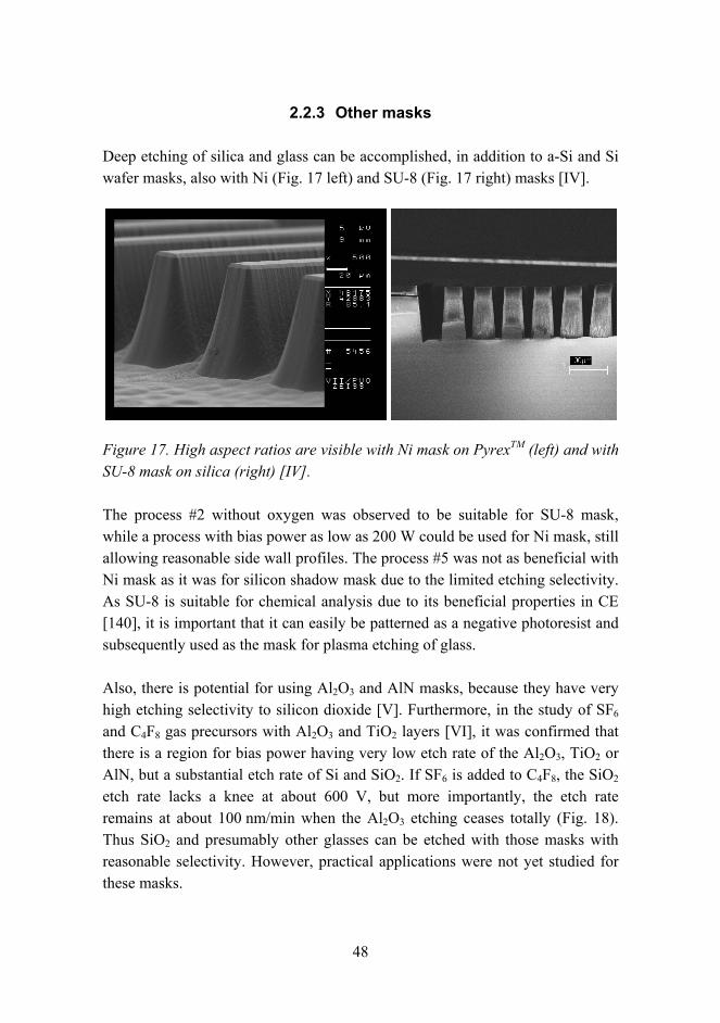
48
2.2.3 Other masks
Deep etching of silica and glass can be accomplished, in addition to a-Si and Si wafer masks, also with Ni (Fig. 17 left) and SU-8 (Fig. 17 right) masks [IV].
Figure 17. High aspect ratios are visible with Ni mask on PyrexTM (left) and with SU-8 mask on silica (right) [IV].
The process #2 without oxygen was observed to be suitable for SU-8 mask, while a process with bias power as low as 200 W could be used for Ni mask, still allowing reasonable side wall profiles. The process #5 was not as beneficial with Ni mask as it was for silicon shadow mask due to the limited etching selectivity. As SU-8 is suitable for chemical analysis due to its beneficial properties in CE [140], it is important that it can easily be patterned as a negative photoresist and subsequently used as the mask for plasma etching of glass.
Also, there is potential for using Al2O3 and AlN masks, because they have very high etching selectivity to silicon dioxide [V]. Furthermore, in the study of SF6 and C4F8 gas precursors with Al2O3 and TiO2 layers [VI], it was confirmed that there is a region for bias power having very low etch rate of the Al2O3, TiO2 or AlN, but a substantial etch rate of Si and SiO2. If SF6 is added to C4F8, the SiO2 etch rate lacks a knee at about 600 V, but more importantly, the etch rate remains at about 100 nm/min when the Al2O3 etching ceases totally (Fig. 18). Thus SiO2 and presumably other glasses can be etched with those masks with reasonable selectivity. However, practical applications were not yet studied for these masks.

49
Figure 18. Etch rates of Al2O3 and SiO2 for two processes with 17 sccm C4F8. The other process has also SF6 at 70 sccm.
2.2.4 The difference between silica and PyrexTM
Disregarding the cleavage having an effect on the observed side wall profiles, the real profiles obtained were between 80° and 86°. PyrexTM was observed to follow the same etch characteristics as silica with a less convex bottom and a slightly lower etch rate. The only major difference observed was the production of non-volatile etching products on the internal parts of the etching chamber, which forced the plasma chamber to be cleaned after about 20 hours of etching PyrexTM. The re-deposition of the etch residues from the chamber walls to the next wafer to be etched was this way avoided. PyrexTM is however suitable for thermal bonding processes so the demonstrative devices were fabricated on PyrexTM.

50
2.2.5 Application
In Fig. 19, a practical application of a nozzle for an atmospheric pressure chemical ionisation (APCI) chip is shown. The etch depth is 250 µm and the final aspect ratio is about 8:1 in average. The walls of the nozzle are slightly below 90° due to the lateral erosion of the silicon shadow mask. The striations of the walls are smoothened out after bonding of the PyrexTM nozzle to a flat PyrexTM cover wafer at 660 °C (Fig. 20). With anisotropic etching it is possible to choose the width and height of the rectangular nozzle independently and even to utilize pillars at the nozzle to further decrease the aperture. This has been shown to affect on the shape of the liquid spray from the nozzle.
Figure 19. PyrexTM nozzle with positive aspect ratio of 8:1, etched with silicon shadow mask [IV].
Figure 20. The roughness of the walls of the PyrexTM nozzle are smoothened after bonding of another PyrexTM wafer at 660 °C.
51
From Fig. 15 it can be estimated that by using the processes described earlier, a single silicon shadow mask can be used twice (2 x 10 hours) for about 350 µm deep via holes of about 200 µm width. After that the bottom of the aperture of the shadow mask starts to widen. Clearly, the required etch depth may be smaller than a full-thickness silica wafer, allowing the total number of the etched wafers to increase.
It was also observed that the number of the silica wafers that can be etched with a single shadow mask depends strongly on the width of the required features. As the polymer preferably deposits on the walls and the surface of the silicon mask, using silicon mask as thin as possible is preferable for small features. Via-holes into a 500 µm silica wafer, which are below 200 µm in diameter, are difficult to realise. A high etching selectivity process such as #1 or #2 in Table 1 can not be used because of the high aspect ratio involved. For a low aspect ratio etching to 500 µm depth, less than about 30 µm silicon, either as a thinned wafer or as an a-Si film, should be a sufficient mask. Also, a-Si would always be a single time mask requiring subsequent chemical removal. If via-holes starting from 200 µm upwards are sufficient, they can be realised on at least two silica wafers with a full-thickness silicon mask put on the top of the silica wafer, simplifying and speeding up the process substantially. This way, more than 100 000 via-holes can be etched on one 150 mm wafer. If 400 µm deep features exceed about 500 µm in width, a high selectivity process (about 20:1) can be utilised. Achieving etched depths of 400 µm of silica consumes about 20 µm Si so the number of silica wafers per one silicon mask wafer exceeds 10, still being limited mainly by faceting i.e. lateral erosion.
If the deep plasma etching is preceded by other process steps, alignment of the shadow mask to those features introduces possible problems. They can be reduced by using e.g. a miniature amount of adhesive between the wafers in aligned bonding equipment or by using a pair of squeezers set on the opposite edges of the stack, when the stack is transferred to the etching chamber. The other options are using pieces of a tape at the edges of the stack or etching alignment pins on one of the wafers and the corresponding dents on the other.

52
2.3 Cavity matrices
2.3.1 Passive cavity matrices
Three types of uncovered cavity matrices (Fig. 21) connected with channels of different width were used in this thesis. They were designed, fabricated and used for the evaluation of the capillary action for silicon and silica surfaces.
Figure 21. The matrix for sequential filling (left), the matrix for parallel filling and the matrix for both sequential and simultaneous filling (right).
After plasma etching of silicon to 400 µm depth and silica to 150 µm depth, the silicon and silica surfaces were oxidized by three different treatments; O2 plasma in STS AOE for 5 min, standard clean (SC1, H2O2:NH4F:H2O 1:1:5) at 65 °C for 10 min and hydrogen peroxide (H2O2:H2O 1:9) with 1:1000 of a commercial surfactant for 5 min.
Three fluids and the three oxidized, i.e. hydrophilic, surface types were combined for a qualitative evaluation of filling time for each type of cavity matrix. De-ionized and distilled water (DIW), Sigma DMEM D5546 cell culturing medium and standard cow milk were used for the experiments. All the oxidizing surface treatments of this work are effective in removing carbon compound residues from surface so they can be used to recover the surface.
53
2.3.2 Surface analysis
All surface types were analyzed for morphology with Atomic Force Microscopy (AFM). As is well known, polished silicon is one of the most planar and smooth surfaces that can be produced. Surface roughness was first measured for prime silicon, showing very smooth surface with root mean square (RMS) roughness of less than 2 Å. Fused silica wafers were observed to have more scratches and long-wavelength thickness variations being, however, highly dependent on manufacturer.
The oxidizing treatments were generally observed to slightly increase the observed surface roughness. Considering the possible effect of surface charge in a thin oxide layer due to oxidizing treatments, the real surface topography can not be distinguished from prime silicon. Prime fused silica is rougher than silicon as received from factory and the change in roughness due to oxidizing treatments could not be observed. Silica surfaces can be polished with e.g. chemical-mechanical polishing (CMP) equipment to achieve smoother surface [141].
Plasma etching induces roughness depending on the material to be etched, the process conditions as well as on the mask material. Even if the etching selectivity is high, the plasma etching of a-Si mask off the silica surface induces significant roughness on the exposed silica. Dry etching of silicon dioxide mask off the silicon also leaves a rough surface.
Silicon experiences increased short period roughness due to SC1, H2O2 or O2 treatments even after plasma etching, but this could only be observed through capillary action experiments discussed in the next section. Plasma etching induces very rough morphology with hundreds of nanometers of height to silicon (Fig. 22 left) with an RMS roughness of about 200 Å. When an oxide mask is plasma etched from top of silicon, the remaining roughness of the silicon surface is different (Fig. 22 center), but the RMS roughness is still about 40 Å. Silica surface is not changed in measurable quantities in oxidizing treatments, and also initial roughness after plasma etching is finer than that of silicon (Fig. 22 right), yielding RMS roughness of less than 20 Å.

54
Figure 22. AFM visualization on surface morphology. On the left silicon after non-ideal plasma etching, in the middle silicon after plasma etching of thermal oxide mask and on the right fused silica after plasma etching.
2.3.3 Critical channel width
To the author�s knowledge, this type of study of capillary action on different surfaces has not been done earlier. Capillary action was observed to depend on the oxidizing treatment on the silicon and glass channel surfaces, but also on the width of the channel. The results of capillary action for the most informative cavity matrix (Fig. 21 right) are listed in Table 3. For this layout having 110 µm channel width next to the large injection well, the channel width increases by 10 µm increments at each T-crossing. As the channel width increases, filling speed appeared to decrease. For some combinations of fluid and surface type, the fluid eventually stops at some T-crossing or channel. For example, the maximum channel width of 110 µm in Table 3 states that the meniscus did not advance into the channel matrix at all and the maximum channel width of 200 µm states that the whole matrix was filled with fluid. Any value between 110 and 200 µm states that the meniscus stops at a crossing with the given channel width.
55
Table 3. The results for different surfaces and fluids with maximum channel width for self-feeding to proceed.
Substrate Final treatment Liquid Max. channel width ------------------------ ------------------ ----------- ------------------------ Dry-etched silicon O2 DIW 190 µm DMEM < 100 µm Milk 110 µm SC1 DIW 170 µm
DMEM > 200 µm Milk > 200 µm
H2O2 DIW > 200 µm DMEM > 200 µm Milk > 200 µm ---------------------- ------------------ ------------ ------------------------ Dry-etched silica O2 DIW 170 µm DMEM 130 µm SC1 DIW > 200 µm DMEM 170 µm H2O2 DIW 150 µm DMEM 150 µm
The dry-etched silicon surface used for capillary action experiments (Fig. 22 left) is more hydrophilic than the dry-etched silica surface (Fig. 22 right). The capillary action was observed to be strongest for H2O2-treated silicon, which allowed rapid filling of all channels to 200 µm width. SC1 treatment, although having H2O2 as one its components, allowed slower movement of DIW to the silicon channels and cavities. O2 showed the least hydrophilic surface for both silicon and silica. Silicon surfaces treated with O2 plasma showed slow advancement of protein containing fluids (milk and DMEM), but no upper limit for channel width was observed. DIW on silicon and both DIW and DMEM on silica stopped totally without reaching 200 µm channels. DIW moved faster but stopped totally when reaching the channel of width of 190 µm. Thus the surface roughness in this range and bulk material seemingly has an impact on capillary action, but apparently the chemical structure and the level of oxidation of a surface and its charge are also important factors for hydrophilicity.
With very hydrophilic surfaces, channel width plays no major role. The two other matrices in Fig. 21 showed very similar results. If the H2O2-treated surfaces
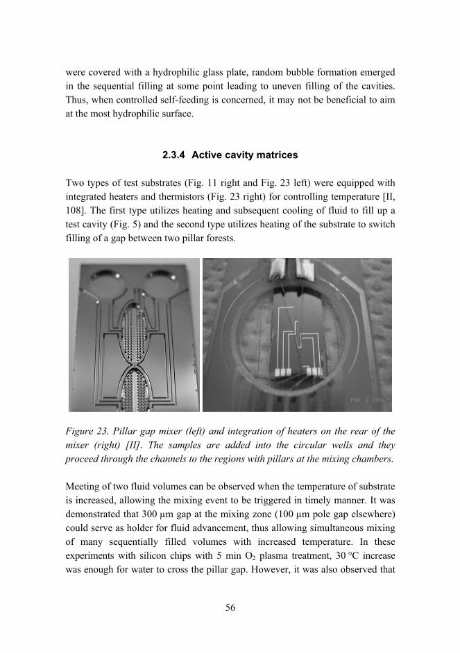
56
were covered with a hydrophilic glass plate, random bubble formation emerged in the sequential filling at some point leading to uneven filling of the cavities. Thus, when controlled self-feeding is concerned, it may not be beneficial to aim at the most hydrophilic surface.
2.3.4 Active cavity matrices
Two types of test substrates (Fig. 11 right and Fig. 23 left) were equipped with integrated heaters and thermistors (Fig. 23 right) for controlling temperature [II, 108]. The first type utilizes heating and subsequent cooling of fluid to fill up a test cavity (Fig. 5) and the second type utilizes heating of the substrate to switch filling of a gap between two pillar forests.
Figure 23. Pillar gap mixer (left) and integration of heaters on the rear of the mixer (right) [II]. The samples are added into the circular wells and they proceed through the channels to the regions with pillars at the mixing chambers.
Meeting of two fluid volumes can be observed when the temperature of substrate is increased, allowing the mixing event to be triggered in timely manner. It was demonstrated that 300 µm gap at the mixing zone (100 µm pole gap elsewhere) could serve as holder for fluid advancement, thus allowing simultaneous mixing of many sequentially filled volumes with increased temperature. In these experiments with silicon chips with 5 min O2 plasma treatment, 30 °C increase was enough for water to cross the pillar gap. However, it was also observed that

57
it is rather difficult to find a stable combination for surface structure, hydrophilicity and fluid composition such that the change in temperature can be considered as the only triggering parameter in repeatable manner. Principally, the triggered filling over an area of surface allows mixing of liquids with different composition, but any substantial difference between properties of the two fluids makes the optimization of the surface even trickier.
The capillary action either competes with or adds to hydrodynamic enforcement, when filling of a sealed cavity is concerned. When fluid is forced to move into cavity with pressure difference between the inside and outside of a sealed cavity, it is apparent that capillary action induced by hydrophilic surfaces adds to penetration depth of fluid into cooling substrate. On hydrophobic surface the initial sealing of cavity with the fluid would have been problematic due to bubble formation to the hydrophobic cavity. As an example, for a hydrophilic surface ( VL cosγ θ = 60 mN/m in Eq. 5) and 500 x 250 µm channel between the elliptic and working volumes, the capillary force equals 90 µN, which translates to 720 Pa. This overpressure over meniscus is compensated when the meniscus advances 720/100 000 = 0.72 % of the sealed air volume. To avoid even this minor offset, surfaces as neutral as possible were prepared for chips shown in Fig. 5 and 11 (right). Apparent contact angle close to 90° was achieved by a short oxygen plasma treatment [I], after fluorine based plasma etch for both silicon and silica (Table 4).
Table 4. O2 plasma process after plasma etching yielding �neutral� surfaces.
Time (s)
O2 (sccm)
Platen (W)
Coil (W)
Pressure (mTorr)
10 100 100 1800 15
With the neutral surface, the difference between initial temperature of substrate and the temperature of the surroundings translates to partial filling of sealed volume by equation of state. Filling of 2 µl test cavity was experimented with working volume of 30 µl and it was observed that temperature difference of 20 °C (about 6.5 % in absolute temperature) was more than enough to fill up the test cavity, leading to an assumption that the surfaces were rather hydrophilic than hydrophobic. Since the working droplet was placed on both of the feeding cavities freely in the air, thermal expansion was not allowed to interfere in the results.

58
In this thesis, pillars were used for enhanced capillary action, but also for confining an area for SPE with beads (Fig. 24). In SPE, an analyte is adsorbed onto large surface area of agarose beads of size from 50 to 90 µm (Fig. 24 left). The original width of the confining poles was 15 µm, their spacing was 35 µm and their height was about 400 µm (Fig. 24 right).
The adsorption of labelled analyte is visible in Fig. 25 as SPE signal. At about 230 s the formed complexes are eluted from the agarose surface by switching a high voltage for capillary electrophoresis on and the fluorescence in the SPE well starts to decrease. At about 300 s, the CE has carried the analyte to the end of the 50 mm long channel and LIF from the labeled analyte experiences a sharp peak (�CE� in Fig. 25).
Figure 24. Solid phase epitaxy beads (left) trapped by pillars from entering the capillary electrophoresis channel (right).
59
0
100
200
300
400
500
600
700
800
900
1000
50 100 150 200 250 300 350 400time (s)
Fluo
resc
ence
inte
nsity
(arb
. uni
ts) SPE
CE
Figure 25. Fluorescence measured in the SPE well imaged in Fig. 24 (�SPE�) and in the end of 50 mm long CE channel (�CE�).
2.4 Patterning hydrophobic surfaces
2.4.1 The shadow mask method
The hydrophobic fluorocarbon coatings were deposited using STS AOE equipment. When the bias power is low enough, net deposition of polymer occurs from the C4F8 gas precursor. The apparent contact angle for hydrophobic coatings was measured to be 106�109° and the figure was very little changed by varying the process parameters, such as pressure, platen temperature, gas flow and source power or deposition time.
Spherical hydrophilic openings in the fluorocarbon coating were produced by putting a shadow mask with etched round holes, sized from 100 µm to 2 mm, on a wafer with the fluorocarbon polymer layer and exposing the stack to O2 plasma, as depicted in Fig. 26. The substrate wafer with the fluorocarbon polymer layer was not cleaned prior the deposition of the polymer, so it only had a native silicon dioxide layer present. The deposition and O2 plasma conditions are listed in Table 5 and they were maintained throughout the experiments.
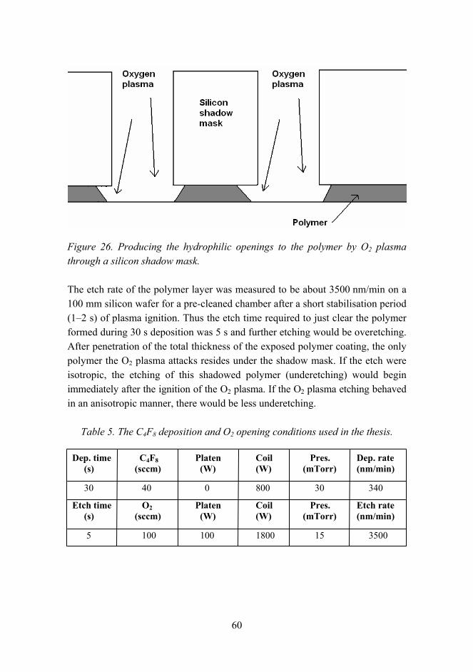
60
Figure 26. Producing the hydrophilic openings to the polymer by O2 plasma through a silicon shadow mask.
The etch rate of the polymer layer was measured to be about 3500 nm/min on a 100 mm silicon wafer for a pre-cleaned chamber after a short stabilisation period (1�2 s) of plasma ignition. Thus the etch time required to just clear the polymer formed during 30 s deposition was 5 s and further etching would be overetching. After penetration of the total thickness of the exposed polymer coating, the only polymer the O2 plasma attacks resides under the shadow mask. If the etch were isotropic, the etching of this shadowed polymer (underetching) would begin immediately after the ignition of the O2 plasma. If the O2 plasma etching behaved in an anisotropic manner, there would be less underetching.
Table 5. The C4F8 deposition and O2 opening conditions used in the thesis.
Dep. time C4F8 Platen Coil Pres. Dep. rate (s) (sccm) (W) (W) (mTorr) (nm/min)
30 40 0 800 30 340
Etch time O2 Platen Coil Pres. Etch rate (s) (sccm) (W) (W) (mTorr) (nm/min)
5 100 100 1800 15 3500

61
It is possible that the underetching extends further in the case of a thicker coating, because there would then be more room for oxygen radicals to penetrate beneath the mask. It is also possible that the underetching extends further in the case of a thinner coating because of microloading, i.e. there is less polymer visible that is to the plasma and it is removed more efficiently.
Underetching of the O2 plasma, i.e. penetration beneath the shadow mask, was examined under a microscope. Also, the duration of the O2 plasma treatment for opening the fluorocarbon coating was plotted against apparent hydrophilicity of the opened area. The apparent hydrophilicity of the openings was considered in terms of the inclination of the silicon substrate required for an aqueous droplet to start rolling due to gravity. The required inclination depends on the size of the droplet in such a way that larger droplets flow on a less inclined surface than smaller droplets do. For a hydrophobic surface and a large droplet (> 100 µl) the required inclination is a few degrees, while on a hydrophilic surface droplets do not roll at any inclination, but they spread leaving a tail behind.
Furthermore, the determination of the underetching may depend on the location on the polymer in the vertical direction i.e. at the silicon surface or at the maximum extent of the O2 plasma or just beneath the shadow mask. The extent of the underetching actually appeared more difficult to see for coatings less than about 500 nm thick because of the lack of interference patterns. However, the maximum reach of the O2 plasma was observed to increase proportionally to the square root of the O2 plasma exposure time and to the thickness of the coating.
2.4.2 The circular openings in the hydrophobic coating
The silicon etching process was adjusted so that 300 µm apertures on the silicon dioxide mask used for patterning the silicon shadow mask wafer yielded 300 µm holes at the base of the shadow mask. Generally, for features of the same size, plasma etching of silicon could be adjusted so that the aperture in question achieves the designed size on the base of the mask. Due to RIE lag a process with more undercut was used so that all the holes went through the silicon wafer approximately at the same time with the exception of 100 µm holes. Thus larger openings ended up wider as designed, while smaller openings ended up smaller than designed. For instance, 800 µm apertures on the silicon dioxide mask ended

62
up as 980 µm holes at the bottom of the silicon wafer and 200 µm apertures ended up as 115�135 µm holes. Thus the aperture size in the silicon shadow mask wafer is different on the top and at the base. Etching 100 µm holes through the wafer would only require more time but should be done on a carrier to protect the electrode from the plasma discharge. The etching on a carrier also causes a significant increase in lateral etching due to increased heating of the substrate so hole diameters at the backside of the wafer would be much larger then the designed dimension.
The capability of the hydrophilic openings to hold aqueous droplets of different sizes sessile was used to study the hydrophilicity of the silicon surface after the O2 plasma exposure of different periods of time. Aqueous droplets of few millimetres in diameter were dispensed on a group of hydrophilic openings surrounded by the hydrophobic area. The substrate was tilted until the droplets slided away. According to Eq. (3), the required inclination depends on the size of the droplet so that larger droplets roll on a less inclined surface than smaller droplets. According to Eq. (2), the hydrophobic adhesion can be calculated for larger droplets and the knowledge of the dynamic advancing and receding angles becomes unimportant, since the angles are independent of the size of the droplet.
For the hydrophilic oxidized silicon surface droplets do not roll at any inclination, but they slide and deform leaving an adsorbed water tail behind. For the non-patterned coatings, i.e. without O2 plasma exposure, the minimum volume of the rolling droplet was initially about 8 µl for substrate inclination of 90°, depending slightly on the deposition conditions. In other words, the gravitational force associated with an 8 microliter droplet is equivalent to 80 µN, when the substrate is tilted 90°, and it is just enough to overcome the adhesion due to the hydrophobic surface. The volumes were about 11 µl for 45° and about 100 µl for 10° inclined substrates. The width of droplets of few sizes on the hydrophobic surface at a contact angle of θ = 105° can be calculated and they are listed in Table 6. Also the adhesion force of a non-patterned 90° surface under the droplet and the (average) number of hydrophilic openings with 1 mm pitch undersiding the droplet are listed.

63
Table 6. The physical parameters of a few droplet sizes on hydrophilic openings.
Droplet volume 8 µl 20 µl 40 µl Weight 80 µN 200 µN 400 µN Width on surface 2.7 mm 3.7 mm 4.6 mm Adhesion force 80 µN 105 µN 130 µN Number of openings 8 14 18
The results of the minimum rolling volumes in Fig. 26 are plotted for opening matrices with 200, 300 and 400 µm designed apertures on the top of the silicon mask with 1 mm pitch. The widths of the final holes on the base of the shadow mask and on the hydrophobic coating were about 125, 300 and 500 µm, respectively. As can be seen from Fig. 27, the minimum rolling volume increases as the O2 plasma treatment time is increased. For 3 min O2 plasma exposure, a droplet of up to 24 µl volume (240 µN) can be held at place on the top of 125 µm hydrophilic sites, when the surface is tilted 90°. The minimum adhesion force of hydrophobic surface for w = 3.9 mm equals about 115 µN. Thus, according to Eq. (3), to allow rolling of the 24 µl droplet, but not smaller ones, on a surface tilted at 90°, the adhesion due to the 12 hydrophilic openings covered by the droplet should be equal to 125 µN.
Figure 27. Minimum volume for an aqueous droplet to begin rolling following placement on a patterned fluorocarbon polymer surface inclined at 90° for 125, 300 and 500 µm hydrophilic openings with 1 mm pitch [I].
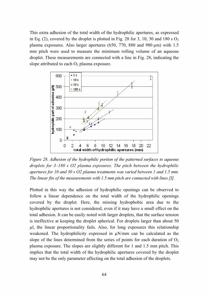
64
This extra adhesion of the total width of the hydrophilic apertures, as expressed in Eq. (2), covered by the droplet is plotted in Fig. 28 for 3, 10, 30 and 180 s O2 plasma exposures. Also larger apertures (650, 770, 880 and 980 µm) with 1.5 mm pitch were used to measure the minimum rolling volume of an aqueous droplet. These measurements are connected with a line in Fig. 28, indicating the slope attributed to each O2 plasma exposure.
Figure 28. Adhesion of the hydrophilic portion of the patterned surfaces to aqueous droplets for 3�180 s O2 plasma exposures. The pitch between the hydrophilic apertures for 10 and 30 s O2 plasma treatments was varied between 1 and 1.5 mm. The linear fits of the measurements with 1.5 mm pitch are connected with lines [I].
Plotted in this way the adhesion of hydrophilic openings can be observed to follow a linear dependence on the total width of the hydrophilic openings covered by the droplet. Here, the missing hydrophobic area due to the hydrophilic apertures is not considered, even if it may have a small effect on the total adhesion. It can be easily noted with larger droplets, that the surface tension is ineffective at keeping the droplet spherical. For droplets larger than about 50 µl, the linear proportionality fails. Also, for long exposures this relationship weakened. The hydrophilicity expressed in µN/mm can be calculated as the slope of the lines determined from the series of points for each duration of O2 plasma exposure. The slopes are slightly different for 1 and 1.5 mm pitch. This implies that the total width of the hydrophilic apertures covered by the droplet may not be the only parameter affecting on the total adhesion of the droplets.

65
From Eq. (1), as the surface tension of the openings after 3 s O2 plasma equals about 18 µN/mm, it translates to the value of 76° for the contact angle. For 3 min exposure the calculated slope in Fig. 28 becomes about 31 µN/mm, translating to the contact angle of about 65°. For 1 mm pitch the slopes are slightly steeper and for 3 min exposure (the maximum hydrophilicity) the difference between the slopes for 1 and 1.5 mm pitch is significant.
The platen electrode temperature was varied from -10 to 60 °C as one of the parameters. The fluorocarbon coating deposited at -10 °C appeared more adhesive shortly after the deposition. The coating even had 20 µl aqueous droplets bound to the non-patterned surface, while the other depositions allowed movement of 10 µl or less droplets on a 90° inclined substrate. The next day, adhesion of an aqueous droplet to the coating had almost reached the value observed for the higher temperature depositions. The reason was not studied. Otherwise the fluorocarbon depositions retained their properties for several days until their adhesion to the surface became weaker. However, the hydrophilic surface treated with O2 plasma retained its hydrophilicity for longer periods of time.
The patterning method can be used for manipulation of droplets on specific reaction sites according to their size. Patterning of the hydrophobic plasma polymer can also be used for patterning cell growth on glass or silicon surfaces as well (Fig. 29 left). The adherence of kidney and prostata cells on hydrophilic glass surface can also be accomplished in three dimensions (Fig. 29 right).
Figure 29. Kidney cells adhere to hydrophilic surface, but not on hydrophobic plasma polymer (left). Prostata cells are adhering to hydrophilic glass wall (right).
66
2.5 Microchip materials for polymerase chain reaction
2.5.1 Quantitative PCR
This thesis introduces a novel method to evaluate the biocompatibility of different surfaces. This is done by studying the suitability of different macro surfaces to PCR. The studied surfaces are the most interesting ones for microfabricated PCR containers. The idea behind the method is to evaluate the suitability of PCR container materials and surfaces without having to fabricate functioning PCR chambers completely. To obtain a large amount of information in a short time, 96-well Applied Biosystems 7500 Fast Real-Time PCR System was used. The qPCR was performed by using SYBR Green chemistry with Dynamo Hot Start SYBR Green qPCR kitTM [VIII] with ROXTM passive reference label.
The excitation of both labels is done with a short tungsten lamp exposure at 72 °C and the 96-well plate is simultaneously read with a CCD camera. Different template amounts from 101 to 106 copies per reaction and parallel reactions were used to evaluate the reliability of the performed PCR and to evaluate the possible effect of template amount to PCR efficiency.
2.5.2 Test surfaces
The test silicon surfaces were introduced as 2 x 2 mm sawed pieces of 0.5 mm thick silicon and fused silica wafers, which had been fusion bonded together beforehand. The inertness of the fused silica was shown without the bonded silicon half.
One test piece was added to each reaction tube fully submerged after mixing, just before performing the PCR. The total volume of a bonded test piece was 4 mm3 (2 x 2 x 1 mm = 4 µl) while the silicon macro surface area was 8 mm2 without considering surface roughness. This is in a good agreement with a microfluidic PCR chip with about 2 µl reaction volume. However, for the 50 µl reaction volume and the test surface, the SVR is rather low at about 0.16 mm2/µl as compared to microchip PCR of 2 µl volume and the inhibition results are not directly applicable into PCR microchambers. The low SVR figure will give optimistic results. It may be possible to produce smaller test pieces which still survive in a vacuum equipment, but decreasing the size of a test piece to for

67
example 1 x 1 x 1 mm and using 4 pieces for each reaction would only increase the total surface area by 4 mm2 (50 %). Another option to increase SVR is to form, say 20 µm wide and 200 µm high, pillars on the wafer before sawing. Then the whole surface would be plasma etched in each case, but the effect of deposited oxides could still be studied. The handling of the pieces would become more difficult, but the gain in surface area increases to 500%.
The test pieces settled to the lower half of each 50 µl reaction well and remained there during the PCR (Fig. 30). The PCR mixture components are assumed to travel throughout the reaction volume due to the changing temperature producing convection and enhanced diffusion. Thus the test surfaces are interacting with the whole reaction volume during the 90 min PCR. PCR reactions without test surfaces were used as references in order to measure the undisturbed amplification in the PCR solution. The inhibitory effect of each test surface was determined by comparing the amplification to the reference reactions without any test surface.
Figure 30. The test surfaces present in the real-time PCR reaction wells [VII].
2.5.3 Fluorescence analysis
The pieces of this size can be treated easily in many types of microfabrication equipment. After sawing the pieces, they were treated differently in order to examine the effect of each treatment on PCR efficiency, as listed in Table 7. The
68
tabulated values are averages over different template amounts, because they showed very little variation to each other in terms of the studied effects.
The PCR amplification curves were analysed in four ways. First the absolute calibrated SYBR Green fluorescence signal from each well was recorded during each cycle. Secondly, the ROX signal, which is not multiplied during PCR, was analyzed to determine the optical shadowing effect of the test pieces. Because both the excitation and the detection of the fluorescence is performed above the plate, the test pieces on the bottom of each reaction well likely shadow a portion of the PCR volume from being excited and detected. However, they do not shadow the whole excited volume, which would be the case if the excitation and detection were performed on opposite sides of the reaction chambers. The possible shadowing effect was taken into account by taking the ratio of the absolute levels of SYBR Green and ROX signals and by comparing it to the ratio values of the reference reactions without the test surfaces.
Thirdly, the detection threshold lag due to the test surfaces was defined as the difference of cycle numbers between the average of the reference reactions and each reaction with a test piece. The threshold was adjusted to the SYBR Green signal exceeding 3 % of the total ROX fluorescence level. The possible lag should give a reasonably good estimation for the level of inhibition during the early PCR, i.e. the exponential region. Finally, to resolve the amplification efficiency in the shift of the exponential regime and the linear regime, the slope of fluorescence signal in this area was observed as this could possibly offer more information about the nature of the inhibition; whether it was due to adsorption of DNA (normal slope) or due to the inefficiency of polymerase or other more extreme condition (decreased slope).
If the fluorescence curve of a reaction is shifted directly right from curve A to curve B as illustrated in Fig. 31, it either implies that the initial amount of the amplifying DNA has been lower in this specific reaction or, the amplification efficiency has been reduced only in the beginning of the cycling due to inefficiency of the polymerase or other reagent. The other PCR components (dNTP, primers or label) exist in a very high concentration and are thus unlikely to affect the amplification efficiency during the first half of the PCR. Then, the PCR may be completed normally and B can reach the same final fluorescence level as A, provided that the number of cycles is sufficient. If, in the case of B,
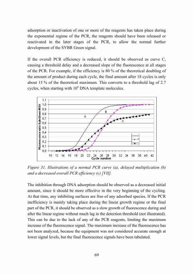
69
adsorption or inactivation of one or more of the reagents has taken place during the exponential regime of the PCR, the reagents should have been released or reactivated in the later stages of the PCR, to allow the normal further development of the SYBR Green signal.
If the overall PCR efficiency is reduced, it should be observed as curve C, causing a threshold delay and a decreased slope of the fluorescence at all stages of the PCR. For example, if the efficiency is 80 % of the theoretical doubling of the amount of product during each cycle, the final amount after 18 cycles is only about 15 % of the theoretical maximum. This converts to a threshold lag of 2.7 cycles, when starting with 106 DNA template molecules.
Figure 31. Illustrations of a normal PCR curve (a), delayed multiplication (b) and a decreased overall PCR efficiency (c) [VII].
The inhibition through DNA adsorption should be observed as a decreased initial amount, since it should be more effective in the very beginning of the cycling. At that time, any inhibiting surfaces are free of any adsorbed species. If the PCR inefficiency is mainly taking place during the linear growth regime or the final part of the PCR, it should be observed as a slow growth of fluorescence during and after the linear regime without much lag in the detection threshold (not illustrated). This can be due to the lack of any of the PCR reagents, limiting the maximum increase of the fluorescence signal. The maximum increase of the fluorescence has not been analyzed, because the equipment was not considered accurate enough at lower signal levels, but the final fluorescence signals have been tabulated.
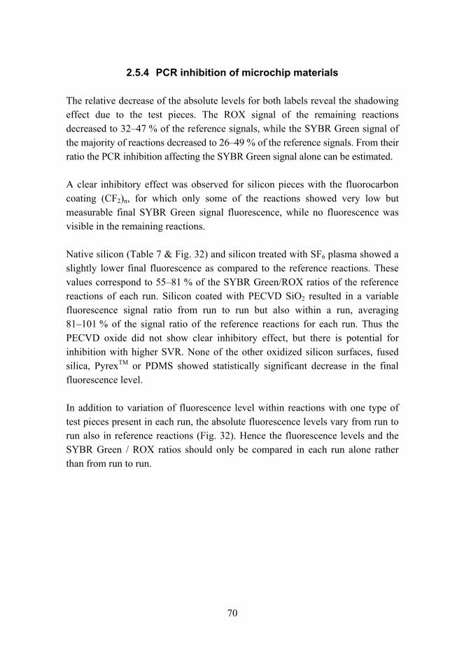
70
2.5.4 PCR inhibition of microchip materials
The relative decrease of the absolute levels for both labels reveal the shadowing effect due to the test pieces. The ROX signal of the remaining reactions decreased to 32�47 % of the reference signals, while the SYBR Green signal of the majority of reactions decreased to 26�49 % of the reference signals. From their ratio the PCR inhibition affecting the SYBR Green signal alone can be estimated.
A clear inhibitory effect was observed for silicon pieces with the fluorocarbon coating (CF2)n, for which only some of the reactions showed very low but measurable final SYBR Green signal fluorescence, while no fluorescence was visible in the remaining reactions.
Native silicon (Table 7 & Fig. 32) and silicon treated with SF6 plasma showed a slightly lower final fluorescence as compared to the reference reactions. These values correspond to 55�81 % of the SYBR Green/ROX ratios of the reference reactions of each run. Silicon coated with PECVD SiO2 resulted in a variable fluorescence signal ratio from run to run but also within a run, averaging 81�101 % of the signal ratio of the reference reactions for each run. Thus the PECVD oxide did not show clear inhibitory effect, but there is potential for inhibition with higher SVR. None of the other oxidized silicon surfaces, fused silica, PyrexTM or PDMS showed statistically significant decrease in the final fluorescence level.
In addition to variation of fluorescence level within reactions with one type of test pieces present in each run, the absolute fluorescence levels vary from run to run also in reference reactions (Fig. 32). Hence the fluorescence levels and the SYBR Green / ROX ratios should only be compared in each run alone rather than from run to run.
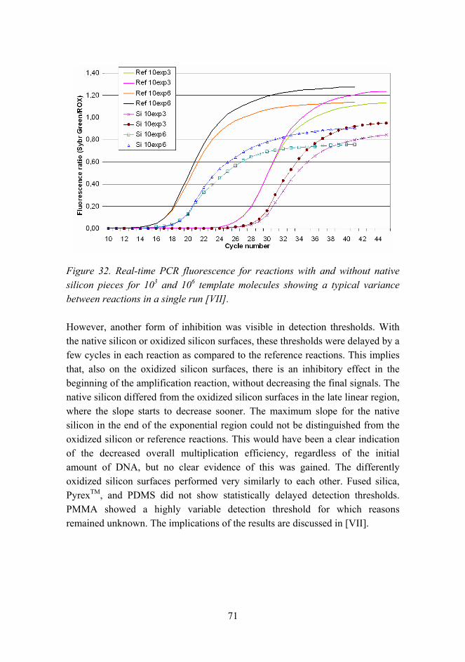
71
Figure 32. Real-time PCR fluorescence for reactions with and without native silicon pieces for 103 and 106 template molecules showing a typical variance between reactions in a single run [VII].
However, another form of inhibition was visible in detection thresholds. With the native silicon or oxidized silicon surfaces, these thresholds were delayed by a few cycles in each reaction as compared to the reference reactions. This implies that, also on the oxidized silicon surfaces, there is an inhibitory effect in the beginning of the amplification reaction, without decreasing the final signals. The native silicon differed from the oxidized silicon surfaces in the late linear region, where the slope starts to decrease sooner. The maximum slope for the native silicon in the end of the exponential region could not be distinguished from the oxidized silicon or reference reactions. This would have been a clear indication of the decreased overall multiplication efficiency, regardless of the initial amount of DNA, but no clear evidence of this was gained. The differently oxidized silicon surfaces performed very similarly to each other. Fused silica, PyrexTM, and PDMS did not show statistically delayed detection thresholds. PMMA showed a highly variable detection threshold for which reasons remained unknown. The implications of the results are discussed in [VII].
72
Table 7. SYBR Green/ROX signal ratio and detection threshold delays with respect to reference reactions in each run. Replicate reactions are shown with different delay values in parantheses.
Test surface Signal ratio Delay in cycles Fused silica 1.06±0.07 0.2±0.5 PyrexTM 1.10±0.09 -0.1±0.8 Silicon 0.63±0.11 2.4±0.6 Plasma SF6 on Si 0.76±0.10 3.3±0.7 Plasma O2 on Si 0.95±0.08 2.7±0.7 (1.2±0.6) H2O2 on Si 0.94±0.07 3.2±0.7 Thermal SiO2 on Si 1.06±0.08 2.7±0.8 (2.2±0.7, 1.1±0.6) PECVD SiO2 on Si 0.90±0.12 2.2±0.1 (1.7±0.4) Plasma SF6 + O2 1.02±0.08 3.1±0.5 (1.9±0.2) Plasma SF6 on thermal SiO2 1.04±0.10 1.2±0.5 (1.3±0.3) Plasma SF6 on PECVD SiO2 0.95±0.09 1.8±0.4 (1.4±0.3) PDMS 0.85±0.09 1.2±1.1 PMMA 0.90±0.12 - (CF2)n coating 0.02±0.01 -
2.5.5 XPS analysis
To examine the adsorbed amount of polymerase and DNA on the O2 plasma treated silicon and the O2 plasma and the H2O2 treated fused silica pieces after PCR, XPS was utilized. XPS provides information about chemical and physical bonds incorporated in the surface layer. The silicon pieces were similar to those in the real-time PCR, but without the bonded fused silica cover. Each silicon piece was pre-treated with SF6 plasma as described, but the silica pieces were not pre-treated. After oxidation, the pieces were introduced to the PCR buffer either with the DNA template (105 per 50 µl reaction) or polymerase (1 unit per 50 µl reaction) and cycled in a PCR cycler. After staying in a poly-propylene tube with the PCR reagent for 4 or 45 cycles, the pieces were moved to another poly-propylene tube and rinsed in DIW for 5 min. Then the pieces were sealed in a poly-ethylene container for subsequent XPS analysis. The analysis was done at three different locations on each surface to include any possible variation in the results due to the location on the test surface.

73
The XPS measurements are shown in Table 8. The DNA contains 19 atomic percent (at-%) oxygen, 32 at-% carbon and 11 at-% nitrogen, while the polymerase contains 9, 32 and 9 at-%, respectively [142]. The polymerase treatment resulted in the highest carbon and nitrogen proportions on both oxidized silicon and silica surfaces. It shows that the used polymerase enzyme is more aggressively immobilized on both of the surfaces than is DNA. H2O2 treatment removes less fluorine from the surface than O2 plasma does, yielding more adsorbed DNA, in form of C and N, on the silica surfaces. The level of C is significant also on the reference pieces without rinsing with a PCR reagent, because the surface adsorbs eagerly any particles containing carbon from atmosphere between the PCR and XPS measurements.
Table 8. The atomic proportions of fluorine, carbon and nitrogen on silicon and silica surfaces after different surface treatments and PCR cycling of 4 or 45 cycles according to XPS. The error range for the absolute atomic composition is about 0.1 %.
Test surface Rinsing F C N None 1.5 % 3.0 % 0.0 % DNA 4 cy. 1.0 % 6.0 % 0.2 % DNA 45 cy. 1.5 % 7.2 % 0.4 %
Plasma O2 on Si
Enzyme 4 cy. 1.2 % 13.9 % 0.9 % None 6.2 % 4.7 % 0.0 % DNA 4 cy. 2.8 % 7.1 % 0.15 %
Plasma O2 on fused silica
Enzyme 4 cy. 2.8 % 10.5 % 0.35 % H2O2 on fused silica DNA 4 cy. 3.3 % 8.6 % 0.25 %
2.6 Evanescent wave fluorescence analysis
2.6.1 Fabrication of the waveguide and the gratings
In this thesis, the detection of fluorescence of fluoresceine was studied with respect to surface sensitivity for a microfluidic device. The detection of DNA with Sybr Green I fluorophor follows the same characteristics as described here for the fluoresceine and more details can be found in [143]. A planar 300 nm
74
thick LPCVD Si3N4 waveguide was used to excite fluorescence by the evanescent field introduced by a laser beam (Fig. 9). Coupling of the 488 nm Ar+ laser (Laser Graphics LGN 4802) beam into the planar waveguide was achieved via 2 x 2 mm grating structures.
Si3N4 was selected because of its high refractive index in contrast to fused silica substrate (Hoya Corp.), silica cover and water to present �the worst case� for surface detection from volume. The penetration of the evanescent field is very limited in high contrast waveguides like this. In the high contrast waveguides, the ratio of power carried by the evanescent field outside the core to the total waveguided power including the core is low. In addition, the field intensity is very high at the surface, emphasizing unintended behaviour of the fluorophor i.e. photobleaching and electronic saturation. Should the fluorophors tend to immobilize on the waveguide surface, the high field region will be overcrowded by the fluorophors leading to their inactivation through clustering. The values for refractive indexes at 488 nm were measured with Filmtek 4000 reflectometer to be 2.024 for LPCVD Si3N4 and 1.462 for SiO2 buffer layer on a silicon wafer. In literature [144], the stoichiometric amorphous Si3N4 has been measured to have a slightly higher index i.e. 2.045.
To fabricate the grating structures into Si3N4, 200 nm 2 % PMMA e-beam resist layer was spun on it. After that 50 nm aluminium layer was sputter deposited on the resist to act as a charge remover. After the e-beam exposure of the grating regions through the Al, it was removed in hydrochloride acid (HCl). Then the PMMA resist was developed in methyl isobutene ketone (MIBK) and the exposed pattern in the PMMA was transferred to Si3N4 by plasma etching in STS AOE. Subsequently, the remains of the PMMA were removed and 1 µm optical SiO2 buffer layer was deposited with PECVD on the top of Si3N4 to fill the etched grooves forming the grating regions. Finally, the optical buffer was removed locally in buffered hydrofluoric acid from the areas to be used for evanescent field excitation.
It is characteristic to the e-beam lithography that the dose on the e-beam resist during the exposure translates to the width of the resist pattern after the developing step. With this in mind, the effects of fabrication errors other than that of lithography, such as a non-ideal etch profile or variation of refractive index, were minimised by a simple procedure. Exposing five grating regions

75
each with different e-beam dose resulted in gratings with slightly different filling factor, thus partially compensating for any reasonable fabrication errors. More precisely, the dose was varied in 10 % steps resulting in gratings between 80 and 120 % dose as compared to an experimental optimum for the designed layer structure. Once the laser power, the width of the collimated beam and the dimensions of the grating and the waveguide are preset, the incidence angle is the only independent variable to be studied.
Rigorous diffraction theory [145] was utilised to achieve optimum (Eq. 6 and 7) right-angled corrugation with 320 nm period and 122 nm depth for the gratings etched into the Si3N4 waveguide core. With the modelled values for the optimum grating period and depth, the grating would now diffract the 488 nm laser beam incident from the normal of the waveguide/grating plane (α = 90°) through its first order (m = -1) exactly to the plane of the waveguide. The Si3N4/SiO2 waveguide supports two TE and two TM modes, when its thickness is between 178 and 354 nm (Eq. 8). The thickness limits for the non-symmetric case of an aqueous droplet with refractive index 1.333 next to the waveguide on one side and silica on the other, are 223 and 376 nm. On the lower limits of both cases, the evanescent field of TM1 mode extends to infinity in silica. On the lower limit of the non-symmetric case, the maximum penetration depth of TM1 into the aqueous medium is limited to about 120 nm.
Among other things, the angle of the maximum diffracted power for a planar grating depends on filling factor of the grating. The filling factor is a measure of the material with the higher refractive index in the grating volume in each period. The value of the filling factor was aimed at 0.5 corresponding to equally sized periods of the higher refractive index and the lower refractive index materials. If the outcome of any of the fabrication steps differed from the designed values, the angle for the incident beam inducing the maximum diffraction efficiency would deviate from the normal angle of the waveguide/grating plane accordingly.
2.6.2 Measurement set-up
The real-time measurement system developed for the thesis allows studying completed PCR chambers. However, the evanescent field approach is not inherently suitable for detecting fluorescence from volume. The approach may
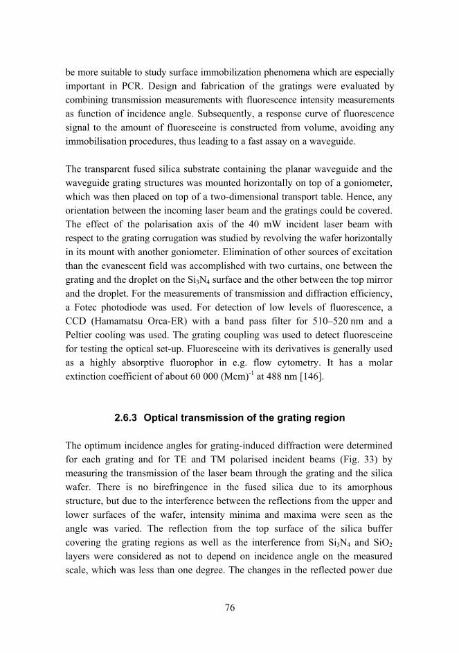
76
be more suitable to study surface immobilization phenomena which are especially important in PCR. Design and fabrication of the gratings were evaluated by combining transmission measurements with fluorescence intensity measurements as function of incidence angle. Subsequently, a response curve of fluorescence signal to the amount of fluoresceine is constructed from volume, avoiding any immobilisation procedures, thus leading to a fast assay on a waveguide.
The transparent fused silica substrate containing the planar waveguide and the waveguide grating structures was mounted horizontally on top of a goniometer, which was then placed on top of a two-dimensional transport table. Hence, any orientation between the incoming laser beam and the gratings could be covered. The effect of the polarisation axis of the 40 mW incident laser beam with respect to the grating corrugation was studied by revolving the wafer horizontally in its mount with another goniometer. Elimination of other sources of excitation than the evanescent field was accomplished with two curtains, one between the grating and the droplet on the Si3N4 surface and the other between the top mirror and the droplet. For the measurements of transmission and diffraction efficiency, a Fotec photodiode was used. For detection of low levels of fluorescence, a CCD (Hamamatsu Orca-ER) with a band pass filter for 510�520 nm and a Peltier cooling was used. The grating coupling was used to detect fluoresceine for testing the optical set-up. Fluoresceine with its derivatives is generally used as a highly absorptive fluorophor in e.g. flow cytometry. It has a molar extinction coefficient of about 60 000 (Mcm)-1 at 488 nm [146].
2.6.3 Optical transmission of the grating region
The optimum incidence angles for grating-induced diffraction were determined for each grating and for TE and TM polarised incident beams (Fig. 33) by measuring the transmission of the laser beam through the grating and the silica wafer. There is no birefringence in the fused silica due to its amorphous structure, but due to the interference between the reflections from the upper and lower surfaces of the wafer, intensity minima and maxima were seen as the angle was varied. The reflection from the top surface of the silica buffer covering the grating regions as well as the interference from Si3N4 and SiO2 layers were considered as not to depend on incidence angle on the measured scale, which was less than one degree. The changes in the reflected power due
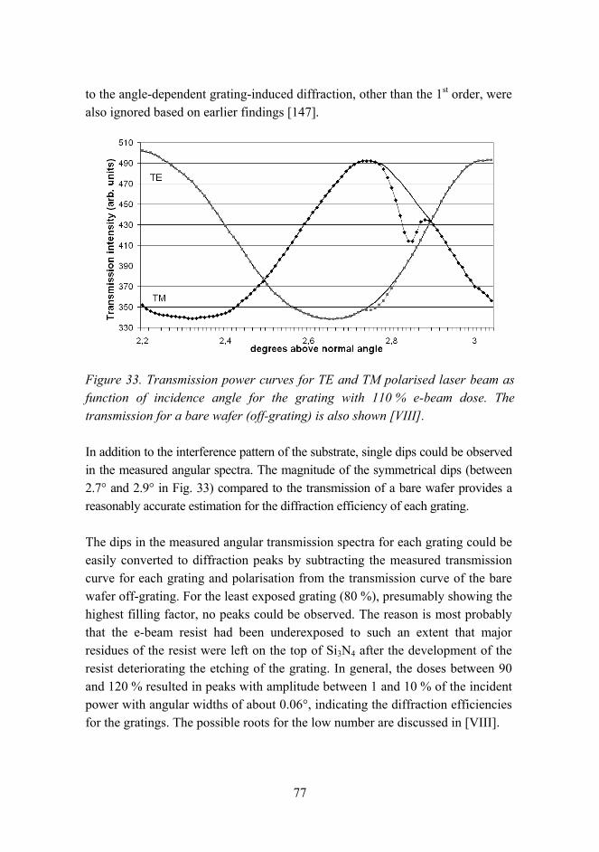
77
to the angle-dependent grating-induced diffraction, other than the 1st order, were also ignored based on earlier findings [147].
Figure 33. Transmission power curves for TE and TM polarised laser beam as function of incidence angle for the grating with 110 % e-beam dose. The transmission for a bare wafer (off-grating) is also shown [VIII].
In addition to the interference pattern of the substrate, single dips could be observed in the measured angular spectra. The magnitude of the symmetrical dips (between 2.7° and 2.9° in Fig. 33) compared to the transmission of a bare wafer provides a reasonably accurate estimation for the diffraction efficiency of each grating.
The dips in the measured angular transmission spectra for each grating could be easily converted to diffraction peaks by subtracting the measured transmission curve for each grating and polarisation from the transmission curve of the bare wafer off-grating. For the least exposed grating (80 %), presumably showing the highest filling factor, no peaks could be observed. The reason is most probably that the e-beam resist had been underexposed to such an extent that major residues of the resist were left on the top of Si3N4 after the development of the resist deteriorating the etching of the grating. In general, the doses between 90 and 120 % resulted in peaks with amplitude between 1 and 10 % of the incident power with angular widths of about 0.06°, indicating the diffraction efficiencies for the gratings. The possible roots for the low number are discussed in [VIII].
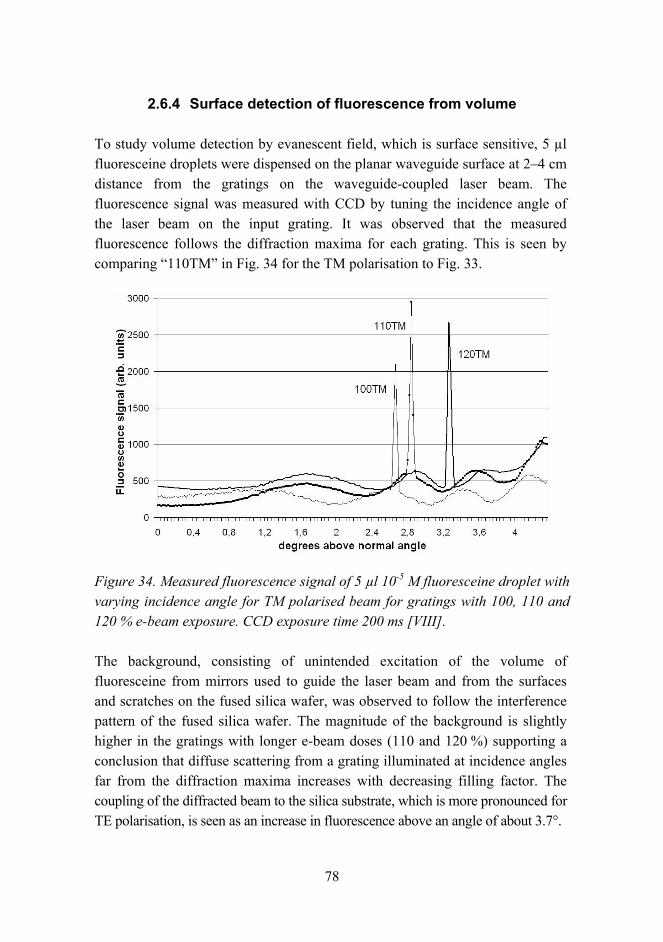
78
2.6.4 Surface detection of fluorescence from volume
To study volume detection by evanescent field, which is surface sensitive, 5 µl fluoresceine droplets were dispensed on the planar waveguide surface at 2�4 cm distance from the gratings on the waveguide-coupled laser beam. The fluorescence signal was measured with CCD by tuning the incidence angle of the laser beam on the input grating. It was observed that the measured fluorescence follows the diffraction maxima for each grating. This is seen by comparing �110TM� in Fig. 34 for the TM polarisation to Fig. 33.
Figure 34. Measured fluorescence signal of 5 µl 10-5 M fluoresceine droplet with varying incidence angle for TM polarised beam for gratings with 100, 110 and 120 % e-beam exposure. CCD exposure time 200 ms [VIII].
The background, consisting of unintended excitation of the volume of fluoresceine from mirrors used to guide the laser beam and from the surfaces and scratches on the fused silica wafer, was observed to follow the interference pattern of the fused silica wafer. The magnitude of the background is slightly higher in the gratings with longer e-beam doses (110 and 120 %) supporting a conclusion that diffuse scattering from a grating illuminated at incidence angles far from the diffraction maxima increases with decreasing filling factor. The coupling of the diffracted beam to the silica substrate, which is more pronounced for TE polarisation, is seen as an increase in fluorescence above an angle of about 3.7°.

79
2.6.5 Fluorescence mapping
For demonstration of parallel detection, five sub-µl droplets of 10-5 M fluoresceine were dispensed on the waveguide surface with 1 mm spacing between the droplet centres (Fig. 35).
Figure 35. Group of 10-5 M fluoresceine droplets with volumes (µl) shown in the left figure. The droplets have 1 mm center spacing and droplets 2 and 3 are located 1 mm aside from the centre of the propagating beam. The evanescent field hits droplet 1 first. The grating with 110 % e-beam dose and TM polarisation was used and CCD exposure time was set to 200 ms [VIII].
The main result is that the intensity maxima for the droplets placed on the beam path were very close to each other and thus one can conclude that the evanescent field is similar for each droplet at the beam path. Three of the droplets were on the path of the guided and coupled beam and two droplets were

80
slightly off the beam path. The first droplet the propagating evanescent field hits (no. 1) had a volume of 1 µl and the next ones (no. 2 and 3 and at the centre) 0.6 µl. Due to the relatively large beam size and its gaussian shape, also the side-droplets (no. 2 and 3) were significantly excited by the evanescent beam. The remaining droplet had a volume of 0.2 µl. It is clearly seen that it is possible to observe fluorescence from a large number of small volumes simultaneously by expanding or splitting the incident beam and increasing the width of the grating area accordingly or, by utilising smaller volumes than demonstrated here.
Cross-talk between neighboring droplets was observed to be minimal. The noise of the laser is generally of the order of 1 % of absolute intensity so it can be neglected. The major limitation for sensitivity was observed to be the uneven distribution of the fluorescence on the waveguide at low concentrations. The secondary limitation appeared to be the noise in the CCD signal, which can also be attributed to the physical phenomena in the vicinity of the waveguide surface i.e. in the evanescent field.
Although the fluorescence in the low end of the concentration scale was unevenly distributed on the surface of the waveguide, the variance can be minimized by averaging over a larger area. If the total area of the droplet was utilised, only excluding the edge reflection peaks, as seen in for DIW between the droplets containing fluoresceine, the limit of detection (LoD) was slightly higher than 10-9 M, which is similar to previous work of other groups [118�132].
The decreased signal in the high end is most likely due to spatial saturation of the high field region or precipitation of fluorophors on the waveguide surface preventing most of the potential emission from taking place. Although it is straightforward to find reproducible and comparable results between the gratings and the incident angles, settling, precipitation or immobilisation of fluoresceine on the waveguide surface causes the fluorescence detection scheme to differ from that of volume detection. Whatever the surface characteristics of Si3N4, they were observed not to have an effect on the linear response of the device in the range between 10-9 M and 10-3 M [VIII]. The LoD can also be calculated by noting the signal level in Fig. 34, which is about 600 times the signal to noise ratio (= 200 LoD) and by multiplying the exposure time of CCD by factor of 50.
81
Finally, the strength and the properties of the evanescent field were evaluated and discussed. The concept of volume detection of fluorescence with a surface sensitive method is defined by both conditions of having a CCD with a collective lens as a detector and of having the initial isotropic distribution of fluorescent label in the droplet of interest. At its best, the volume detection can be realised with a comparable sensitivity to the detection of an immobilised and specific surface layer. The described waveguide sensor can be used to e.g. seal a miniaturised total analysis system (µTAS) chip.
2.6.6 Evolution of fluorescence for evanescent and direct excitation
The signal was observed to vary significantly in the course of the continuous exitation. The evolution of the measured fluorescence can offer valuable information, while it may be difficult to distinguish between several factors. By comparing the fluorescence of direct exposure, where the laser beam directly excites the fluorescent droplet and not through diffraction grating and evanescent field, the surface phenomena e.g. immobilisation and other phenomena e.g. photobleaching can be studied.
The gradual settling of fluorescent matter causes the evanescent signal to increase immediately after introduction as in Fig. 36. When the surface area dependent evaporation of the aqueous droplet starts to take effect, the concentration of fluorophors is increased, finally leading to precipitation of fluorophors in the droplet. For direct exposure, the time evolution is different. The fluorescence yield decreases almost instantly, evidencing the photobleaching being emphasized in the directly excited samples, as compared to evanescent excitation, where it may be screened by other effects.
Heating and evaporation are more efficient in direct exposure and because the fluorophors have only a limited convective reservoir in the volume of the droplet, the bleached or otherwise inactivated molecules are not replaced by fresh molecules after a few minutes. In other words, the replacement of bleached fluorophors due to the large non-excited reservoir in the droplet due to dissociation, convection and diffusion is more effective in the evanescent excitation.
82
Figure 36. Time evolution of fluorescence of 5 µl 10-5 M fluoresceine droplet with direct and evanescent excitation. Exposure times for CCD were 100 µs and 150 ms, respectively [VIII].
It is possible that in the region of high evanescent field strength, the energy levels of the fluorophors, responsible for the fluorescence emission, are saturated. In this work, however, the fluorescence signal was observed to follow linearly the excitation power and no evidence of such a saturation phenomenon was observed.
The direct excitation yields clearly better sensitivity because the excitation power is present in the total depth of the droplet. The relative intensity in the evanescent field in a droplet located on the top of the waveguide, as compared to the field intensity of the laser beam itself, can be calculated. The depth of the evanescent field of TM1 waveguide mode equals about 55 nm for an aqueous fluorescent liquid as coating with ns equal to 1.333 (d in Eq. 9). For the mode, about 9 % of the total propagating power in the mode travels in the water as an evanescent field. For TM0 mode the figure is much lower due to the high effective index of propagation and the corresponding very high confinement, reaching about 1 % of total propagating power. Therefore, it can be expected that almost all the power propagates in the 1st order modes, as previously mentioned, with the measured 10 % coupling efficiency from the incident beam to the waveguide modes. Shrinking of the beam from 1 mm to about 400 nm in
83
one dimension, in the waveguide and its surroundings, leads to 250-fold maximum intensity at the centre of the incident beam, at the centre of the waveguide core and at the centre of the beam path. The intensity distribution in the evanescent field has a maximum at the surface of the waveguide and this maximum is about half of the 250-fold maximum intensity. At 55 nm from the silicon nitride surface into the aqueous phase, the excitation intensity has dropped further by 1/e. For fluoresceine, the direct excitation yielded about 3000-fold initial intensity level as compared to evanescent excitation. Geometrical calculations for 1 mm high droplet yield about 140 times more fluorescence being excited with the direct beam in contrast with the evanescent field (125-fold, 55 nm depth). This result clearly shows that the high evanescent field strength is only able to excite effectively a small percentage of fluorophors in its regime.
84
3. Conclusions
The purpose of this thesis was to report on new advances in fabrication of microfluidic devices for bioanalytical applications. As the main result of the work reported in this thesis, generic and practical processing knowledge has been obtained. The thesis combines new ideas, new design, advanced fabrication and discussion of results with a suitable detection scheme and a novel characterisation method for microfluidic devices.
New technologies have been developed on silicon and glass. The goal has been achieved by demonstrating many deep plasma etching processes for glass with good aspect ratio, high etching selectivity or depth over 350 µm. Especially, the process with a silicon shadow mask has been important and it has therefore been characterized throroughly. Also, microfluidic structures with a demanding lay-out have been etched successfully into silicon.
The goal has also been achieved by showing a new way to pattern hydrophobic plasma-deposited fluorocarbon coating with a silicon shadow mask allowing many interesting properties of the patterned silicon surface. While the hydrophobic plasma polymer has been utilized earlier for e.g. hydrophobic valves, the hydrophilicity of channel matrices fabricated into silicon and glass has been shown to be tunable depending on the oxidation method of the surfaces after fluorine-based plasma etching. Furthermore, a few other microfluidic valving mechanisms requiring no complex parts or processing were demonstrated.
Microfluidic structures often involve polymerase chain reaction, for which a new evaluation method regarding the suitability of different silicon-related surfaces has been demonstrated. By analyzing the real-time fluorescence with test surfaces present, even the mechanisms of possible inhibition can be found. With the studied surface-to-volume ratio, only fluoropolymer coating was observed to be inhibitory to PCR. Many oxidized surface types also showed a lag in the amplification.
One of the most fascinating detection schemes for microfluidic assays, evanescent wave sensing through grating-coupling of laser beam into a planar waveguide, has been characterized. The sensitivity was observed to be about 1 nM fluoresceine even with the coupling efficiency of only 10 %.

85
Future work is seen to consist of three-dimensional channel structures with hydrophobic valves and manipulation of cells with electrodes in a culturing channel matrix and, heterogeneous integration will perhaps follow.

86
References
[1] Erickson D. and Li D., Integrated microfluidic devices, Analytica Chimica Acta 507, pp. 11�26, 2004.
[2] Vilkner T., Janasek D. and Manz A., Micro Total Analysis Systems. Recent Developments, Analytical Chemistry 76, pp. 3373�3386, 2004.
[3] Abgrall P. and Gué A.-M., Lab-on-a-chip technologies: making a microfluidic network and coupling it into a complete microsystem� a review, Journal of Micromechnics and Microengineering 17, R15-R49, 2007.
[4] Weigl B., Bardell R. and Cabrera C., Lab-on-a-chip for drug development, Advanced Drug Delivery Reviews 55, pp. 349�377, 2003.
[5] Huikko K., Kostiainen R. and Kotiaho T., Introduction to micro-analytical systems: bioanalytical and pharmaceutical applications, European Journal of Pharmaceutical Sciences 20 (2), pp. 149�171, 2003.
[6] Fiorini G. and Chiu D.T., Disposable microfluidic devices: fabrication, function, and application, BioTechniques 38, pp. 429�446, 2005.
[7] Manz A. et al., Planar chips technology for miniaturization and integration of separation techniques into monitoring systems: Capillary electrophoresis on a chip, Journal of Chromatography 593, pp. 253�258, 1992.
[8] Harrison D.J., Manz A., Fan Z., Luedi H. and Widmer H.M., Capillary electrophoresis and sample injection systems integrated on a planar glass chips, Analytical Chemistry 64, pp. 1926�1932, 1992.
[9] Seiler K., Harrison D.J., Jed H. and Manz A., Planar glass chips for capillary electrophoresis: repetitive sample injection, quantitation, and separation efficiency, Analytical Chemistry 65, pp. 1481�1488, 1993.

87
[10] Effenhauser C.S., Manz A. and Widmer H., Glass chips for high-speed capillary electrophoresis separations with submicrometer plate heights, Analytical Chemistry 65, pp. 2637�2642, 1993.
[11] Manz A., Graber N. and Widmer H., Miniaturized total analysis systems: a novel concept for chemical sensing, Sensors and Actuators B 1, pp. 244�248, 1990.
[12] Manz A. et al., Micromachining of monocrystalline silicon and glass for chemical analysis systems: A look into next century�s technology or just a fashionable craze?, Trends in Analytical Chemistry 10 (5), pp. 144�149, 1991.
[13] Northrup M., Ching M., White R. and Watson R., DNA amplification in a microfabricated reaction chamber, Transducers ´93, ISBN 4-9900247-2-9, pp. 924�926, 1993.
[14] Bousse L. et al., Micromachined multichannel systems for the measurements of cellular metabolism, Sensors and Actuators B 20, pp. 145�150, 1994.
[15] Sobek D., Young A., Gray M. and Senturia S., A microfabricated flow chamber for optical measurements in fluids, Proc. of MEMS ´93, Fort Lauerdale, USA, pp. 219�224, 1993.
[16] Fuhr G., Glasser H., Müller T. and Schnelle T., Cell manipulation and cultivation under a.c. electric field influence in highly conductive culture media, Biochimica et Biophysica Acta 1201 (3), pp. 353�360, 1994.
[17] Andersson H. and van der Berg A., Microfluidic devices for cellomics: a review, Sensors and Actuators B 92, pp. 315�325, 2003.
[18] Terry S., Jerman J. and Angell J., A gas chromatographic air analyzer fabricated on a silicon wafer, IEEE Transactions on electrical devices 34 ed-26, no 12, pp. 1880�1886, 1979.
[19] Kwang W. and Chong H., A review of microvalves, Journal of Micromechanics and Microengineering 16, R13�R39, 2006.

88
[20] Reyes D., Iossifidis D., Auroux P. and Manz A., Micro total analysis systems. 1. Introduction, theory, and technology, Analytical Chemistry 74, pp. 2623�2636, 2002.
[21] Razzacki Z., Thwar P., Yang M., Ugaz V. and Burns M. Integrated microsystems for controlled drug delivery, Advanced Drug Delivery Reviews 56, pp. 185�198, 2004.
[22] Sauer S. et al., Miniaturization in functional genomics and proteomics, Nature Reviews Genetics 6, pp. 465�476, 2006.
[23] Laser D.J. and Santiago J.G., A review of micropumps, Journal of Micromechanics and Microengineering 14, R35�R64, 2004.
[24] Wijngaart W., Andersson H., Enoksson P. and Stemme G., The first self-priming and bidirectional valve-less diffuser micropump for both liquid and gas, Proc. IEEE 13, pp. 674�679, 2000.
[25] Marmottant P. and Hilgenfeldt S., A bubble driven microfluidic transport element for bioengineering, Proc. of the National Academy of Sciences of the U.S.A, 101 (26), pp. 9523�9527, 2004.
[26] Torkkeli A., Doctoral dissertation: Droplet microfluidics on a planar surface, VTT Publications 504, 2003.
[27] Squires T. and Quake S., Microfluidics: Fluid physics at the nanoliter scale, Reviews of modern physics 77, pp. 977�1007, 2005.
[28] Turner A.P.F., Karube I., and Wilson G.S., Biosensors: Fundamentals and Applications. Oxford University Press, Oxford, 770p, 1987.
[29] http://www.cranfield.ac.uk/biotech/chinap.htm.
[30] Liedberg, B., Nylander C. and Lundström I., Surface plasmon resonance for gas detection and biosensing, Sensors and Actuators A 4, pp. 299�304, 1983.
89
[31] Kulmala S. and Suomi J., Current status of modern analytical luminescence methods, Analytical Chimica Acta 500 (1�2), pp. 21�69, 2003.
[32] Wang J., Microchip devices for detecting terrorist weapons, Analytica Chimica Acta 507, pp. 3�10, 2004.
[33] Becker H. and Gärtner C., Polymer microfabrication methods for microfluidic analytical applications, Electrophoresis 21 (1), pp. 12�26, 2000.
[34] Wilke N., Hibat C., O�Brian J. and Morrissey A., Silicon microneedle electrode array with temprerature monitoring for electroporation, Sensors and Actuators A 123�124, pp. 319�325, 2005.
[35] Griss P. and Stemme G., Side-opened out-of-plane microneedles for microfluidic transdermal liquid transfer, Journal of Microelectromechanical Systems 12 (3), pp. 296�301, 2003.
[36] Kooyman P. and Lechuga L., Handbook of Biosensors and Electronic Noses, pp. 169�196, CRC Press, New York, 1997.
[37] Junker D., Doctoral dissertation: Capillary microfluidic systems for bio/chemistry, University of Neuchatel, 2002.
[38] Jensen M., Mouritsen O. and Peters G., The hydrophobic effect: Molecular dynamics simulation of water confined between extended hydrophobic and hydrophilic surfaces, Journal of Chemical Physics 120 (20), pp. 9729�9744, 2004.
[39] Babukutty Y. et al., Poly(vinyl chloride) surface modification using tetrefluoroethylene in Atmospheric Pressure Glow Discharge, Langmuir 15 (20), pp. 7055�7062, 1999.
[40] Iriyama Y., Yasuda T., Cho D. and Yasude H., Plasma surface treatment on nylon fabrics by fluorocarbon compounds, Journal of Applied Polymer Science 39 (2), pp. 249�264, 1990.
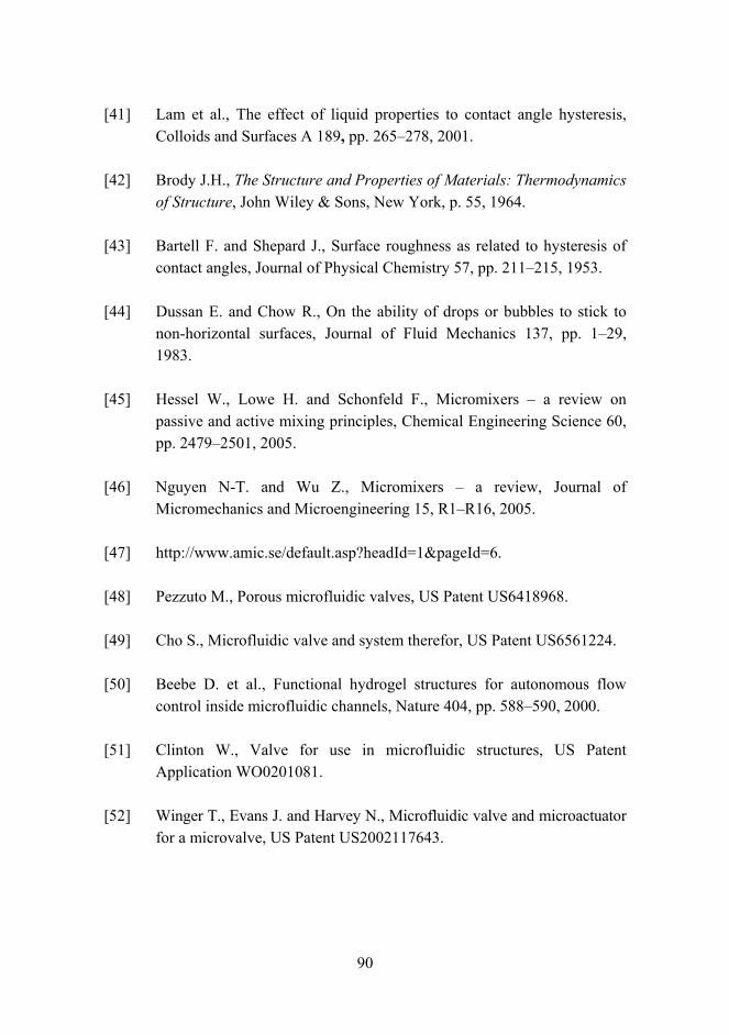
90
[41] Lam et al., The effect of liquid properties to contact angle hysteresis, Colloids and Surfaces A 189, pp. 265�278, 2001.
[42] Brody J.H., The Structure and Properties of Materials: Thermodynamics of Structure, John Wiley & Sons, New York, p. 55, 1964.
[43] Bartell F. and Shepard J., Surface roughness as related to hysteresis of contact angles, Journal of Physical Chemistry 57, pp. 211�215, 1953.
[44] Dussan E. and Chow R., On the ability of drops or bubbles to stick to non-horizontal surfaces, Journal of Fluid Mechanics 137, pp. 1�29, 1983.
[45] Hessel W., Lowe H. and Schonfeld F., Micromixers � a review on passive and active mixing principles, Chemical Engineering Science 60, pp. 2479�2501, 2005.
[46] Nguyen N-T. and Wu Z., Micromixers � a review, Journal of Micromechanics and Microengineering 15, R1�R16, 2005.
[47] http://www.amic.se/default.asp?headId=1&pageId=6.
[48] Pezzuto M., Porous microfluidic valves, US Patent US6418968.
[49] Cho S., Microfluidic valve and system therefor, US Patent US6561224.
[50] Beebe D. et al., Functional hydrogel structures for autonomous flow control inside microfluidic channels, Nature 404, pp. 588�590, 2000.
[51] Clinton W., Valve for use in microfluidic structures, US Patent Application WO0201081.
[52] Winger T., Evans J. and Harvey N., Microfluidic valve and microactuator for a microvalve, US Patent US2002117643.
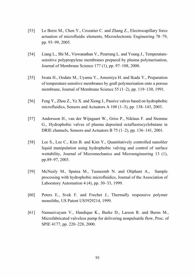
91
[53] Le Berre M., Chen Y., Crozatier C. and Zhang Z., Electrocapillary force actuation of microfluidic elements, Microelectronic Engineering 78�79, pp. 93�99, 2005.
[54] Liang L., Shi M., Viswanathan V., Peurrung L. and Young J., Temperature-sensitive polypropylene membranes prepared by plasma polymerisation, Journal of Membrane Science 177 (1), pp. 97�108, 2000.
[55] Iwata H., Oodate M., Uyama Y., Amemiya H. and Ikada Y., Preparation of temperature-sensitive membranes by graft polymerisation onto a porous membrane, Journal of Membrane Science 55 (1�2), pp. 119�130, 1991.
[56] Feng Y., Zhou Z., Ye X. and Xiong J., Passive valves based on hydrophobic microfluidics, Sensors and Actuators A 108 (1�3), pp. 138�143, 2003.
[57] Andersson H., van der Wijngaart W., Griss P., Niklaus F. and Stemme G., Hydrophobic valves of plasma deposited octafluorocyclobutane in DRIE channels, Sensors and Actuators B 75 (1�2), pp. 136�141, 2001.
[58] Lee S., Lee C., Kim B. and Kim Y., Quantitatively controlled nanoliter liquid manipulation using hydrophobic valving and control of surface wettability, Journal of Micromechanics and Microengineering 13 (1), pp.89�97, 2003.
[59] McNeely M., Sputea M., Tusneemb N. and Oliphant A., Sample processing with hydrophobic microfluidics, Journal of the Association of Laboratory Automation 4 (4), pp. 30�33, 1999.
[60] Peters E., Svek F. and Frechet J., Thermally responsive polymer monoliths, US Patent US5929214, 1999.
[61] Namasivayam V., Handique K., Burke D., Larson R. and Burns M., Microfabricated valveless pump for delivering nonpulsatile flow, Proc. of SPIE 4177, pp. 220�228, 2000.
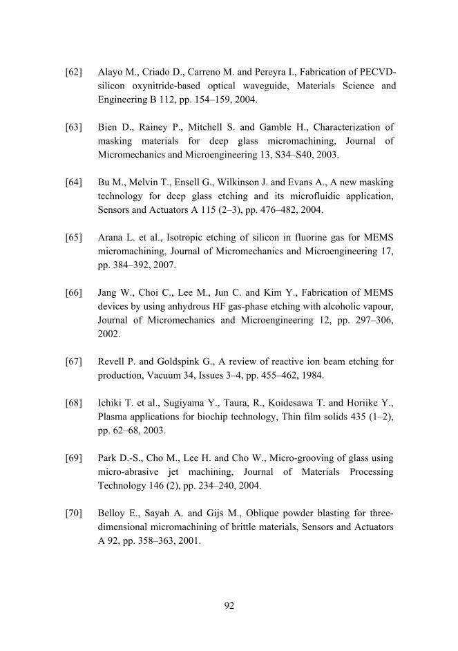
92
[62] Alayo M., Criado D., Carreno M. and Pereyra I., Fabrication of PECVD-silicon oxynitride-based optical waveguide, Materials Science and Engineering B 112, pp. 154�159, 2004.
[63] Bien D., Rainey P., Mitchell S. and Gamble H., Characterization of masking materials for deep glass micromachining, Journal of Micromechanics and Microengineering 13, S34�S40, 2003.
[64] Bu M., Melvin T., Ensell G., Wilkinson J. and Evans A., A new masking technology for deep glass etching and its microfluidic application, Sensors and Actuators A 115 (2�3), pp. 476�482, 2004.
[65] Arana L. et al., Isotropic etching of silicon in fluorine gas for MEMS micromachining, Journal of Micromechanics and Microengineering 17, pp. 384�392, 2007.
[66] Jang W., Choi C., Lee M., Jun C. and Kim Y., Fabrication of MEMS devices by using anhydrous HF gas-phase etching with alcoholic vapour, Journal of Micromechanics and Microengineering 12, pp. 297�306, 2002.
[67] Revell P. and Goldspink G., A review of reactive ion beam etching for production, Vacuum 34, Issues 3�4, pp. 455�462, 1984.
[68] Ichiki T. et al., Sugiyama Y., Taura, R., Koidesawa T. and Horiike Y., Plasma applications for biochip technology, Thin film solids 435 (1�2), pp. 62�68, 2003.
[69] Park D.-S., Cho M., Lee H. and Cho W., Micro-grooving of glass using micro-abrasive jet machining, Journal of Materials Processing Technology 146 (2), pp. 234�240, 2004.
[70] Belloy E., Sayah A. and Gijs M., Oblique powder blasting for three-dimensional micromachining of brittle materials, Sensors and Actuators A 92, pp. 358�363, 2001.
93
[71] Niino H. et al., Kawaguch, Y., Sato T., Narazaki A. and Kurosaki R., Laser ablation of toluene liquid for surface micro-structuring of silica glass, Applied Surface Science 252 (13), pp. 4387�4391, 2006.
[72] Zeng X., Mao X., Wen S., Greif R. and Russo R., Energy deposition and shock wave propagation during pulsed laser ablation in fused silica cavities, Journal of Physics. D: Applied Physics 37, pp. 1132�1136, 2004.
[73] Franssila S., Marttila S., Kolari K., Östman P., Kotiaho T., Kostiainen R., Lehtiniemi R. and Fager C.-M, A miniaturised atmospheric pressure chemical ionisation nebulizer chip, Journal of MEMS 15, p. 1251�1255, 2006.
[74] Kiihamäki J. and Franssila S., Pattern shape effects and artefacts in deep silicon etching, Jornal of Vacuum Science and Technology A 17(4), pp. 2280�2285, 1999.
[75] Franssila S., Introduction to microfabrication, p. 125, John Wiley & Sons Ltd., England, 2004.
[76] The MEMS Handbook, CRC Press, 2006.
[77] Park W.J., Kim Y., Kim J., Suh S. and Yoon D., Etching characterization of shaped hole high density plasma for using MEMS devices, Surface & Coatings Technology 193, pp. 314�318, 2005.
[78] Solehmainen K. et al., Dry-etched silicon-on-insulator wave-guides with low propagation and fiber-coupling losses, Journal of Lightwave Technology 23 (11), pp. 3875�3880, 2005.
[79] Lacroix L.-M. et al., Tuneable rough surfaces: A new approach for elaboration of superhydrophobic films, Surface Science 592, pp. 182�188, 2005.
[80] Milenin A., Jamois C., Geppert T., Gosele U. and Wehrspohn R., SOI planar photonic crystal fabrication: Etching through SiO2/Si/SiO2 layer systems using fluorocarbon plasmas, Microelectronic Engineering 81, pp. 15�21, 2005.
94
[81] Solehmainen K., Aalto T., Dekker J., Kapulainen M., Harjanne M. and Heimala P., Development of multi-step processing in silicon-on-insulator for optical waveguide applications, Journal of Optics A: Pure and Applied Optics 8 (7), pp. S455�S460, 2006.
[82] Alayo M., Criado D., Carreno M. and Pereyra I., Fabrication of PECVD-silicon oxynitride-based optical waveguides, Materials Science and Engineering B 112, pp. 154�159, 2004.
[83] Thienot E., Domingo F., Cambril E. and Gosse C., Reactive ion etching of glass for biochip applications: Composition effects and surface damages, Microelectronic Engineering 83, Issues 4�9, pp. 1155�1158, 2006.
[84] Li X., Abe T. and Esashi M., Deep reactive ion etching of Pyrex glass using SF6 plasma, Sensors and Actuators A, 87 (3), pp. 139�145, 2001.
[85] Li X., Abe T. and Asashi M., Fabrication of High-Density Electrical Feed-Throughs by Deep-Reactive-Ion Etching of Pyrex glass, Journal of Microelectromechanical Systems, 11 (6), pp. 625�630, 2002.
[86] Park J.H., Lee N., Lee J., Park J.S. and Park H.D., Deep dry etching of borosilicate glass using SF6 and SF6/Ar inductively coupled plasmas, Microelectronic Engineering 82, pp. 119�128, 2005.
[87] Akashi T. and Yoshimura Y., Deep reactive ion etching of borosilicate glass using an anodically bonded silicon wafer as an etching mask, Journal of Micromechanics and Microengineering 16, pp. 1051�1056, 2006.
[88] Metwalli E. and Pantano C., Reactive ion etching of glasses: Composition dependence, Nuclear Instruments and Methods in Physics Research B 207, pp. 21�27, 2003.
[89] Leech P.W., Reactive ion etching of quartz and silica-based glasses in CF4/CHF3 plasmas, Vacuum 55, pp. 191�196, 1999.
95
[90] Rodriguez I., Spicar-Mihalic P., Kuyper C., Fiorini G. and Chiu D., Rapid prototyping of glass microchannels, Analytica Chimica Acta 496, pp. 205�215, 2003.
[91] Ceriotti A., Weible K., de Rooij N. and Verpoorte E., Rectangular channels for lab-on-a-chip applications, Microelectronic Engineering 67�68, pp. 865�871, 2003.
[92] Kim G., Kim S. and Kim C., Selective etching of SiO2 over Si3N4 in a C5F8/O2/Ar plasma, Microelectronic Engineering 83, pp. 2504�2509, 2006.
[93] Kwon O., Jin W. and Sawin H., Angular dependence of silicon oxide etching yield in fluorocarbon etching chemistries, Applied Physics Letters 88, Art No. 133117, 2006.
[94] Li X. et al., Effects of Ar and O2 additives on SiO2 etching in C4F8-based plasmas, Journal of Vacuum Science and Technology A 21 (1), pp. 284�293, 2003.
[95] Pang S.W. et al., Pattern transfer by dry etching through stencil mask, Journal of Vacuum Science and Technology B (6), pp. 249�255, 1988.
[96] Zhao Z., Cui Z., Cui D. and Xia S., Monolithically integrated PCR biochip for DNA amplification, Sensors and Actuators A 108, pp. 162�167, 2003.
[97] Shen K., Chen X., Guo M. and Cheng J., A microchip-based PCR device using flexible printed circuit technology, Sensors and Actuators B 105 (2), pp. 251�258, 2005.
[98] Northrup et al., A miniature analytical instrument for nucleic acids based on micromachined silicon reaction chambers, Analytical Chemistry 70, pp. 918�922, 1998.
[99] Woolley A., Hadley D., Landre P., deMello A., Mathies R. and Northrup M., Functional integration of PCR amplification and capillary electrophoresis in a microfabricate.d DNA analysis device, Analytical Chemistry 68, pp. 4081�4086, 1996.

96
[100] Anderson R., Su X., Bogdan G. and Fenton J., A miniature integrated device for automated multistep genetic assays, Nucleic Acid Research 28 (12), e60(i�vi), 2002.
[101] Daniel J.H. et al., Silicon microchambers for DNA amplification, Sensors and Actuators A 71, pp. 81�88, 1998.
[102] Cheng J., Shoffner M., Hvichia G., Kricka L. and Wilding P., Chip PCR II. Investigation of different PCR amplification systems in microfabricated silicon-glass chips, Nucleic Acids Research 24, pp. 380�385, 1996.
[103] Taylor T., Winn-Deen E., Picozza E., Woudenberg T. and Albin M., Optimization of the performance of the polymerase chain reaction in silicon-based microstructures, Nucleic Acids Research 25 (15), pp. 3164�3168, 1997.
[104] Nagai H., Murakami Y., Yokoyama K. and Tamiya E., High-throughput PCR in silicon based microchamber array, Biosensors and Bioelectronics 16, pp. 1015�1019, 2001.
[105] Hu G., Xiang Q., Fu R., Xu B., Venditti R. and Li D., Electrokinetically controlled real-time polymerase chain reaction in microchannel using Joule heating effect, Analytica Chimica Acta 557, pp. 146�151, 2006.
[106] Cho Y. et al., Clinical evaluation of micro-scale chip based PCR system for rapid detection of hepatitis B virus, Biosensors and Bioelectronics 21, pp. 2161�2169, 2006.
[107] Zhang C., Xu J., Ma W. and Zheng W., PCR microfluidic devices for DNA amplification, Biotechnology Advances 24, pp. 243�284, 2006.
[108] Hokkanen A., Koponen J., Stuns I. and Kolari K., Active silicon support for DNA diagnostics, Proc. SPIE 4982-41, pp. 310�318, 2003.
[109] Lagally E., Emrich C. and Mathies R., Fully integrated PCR-capillary electrophoresis microsystem for DNA analysis, Lab on a chip 1, 2001, pp. 102�107.
97
[110] http://de.wikipedia.org/wiki/Polymerase-Kettenreaktion.
[111] Panaro N., Lou X., Fortina P., Kricka L. and Wilding P., Surface effects on PCR reactions in multichip microfluidic platforms, Biomedical Microdevices 6 (1), pp. 75�80, 2004.
[112] Prakash A. et al., Small volume PCR in PDMS biochips with integrated fluid control and vapour barrier, Sensors and Actuators B 113 (1), pp. 398�409, 2006.
[113] Felbel J., Bieber I., Pipper J. and Kohler J., Investigations on the compatibility of chemically oxidized silicon (SiOx)-surfaces for applications towards chip-based polymerase chain reaction, Chemical Engineering Journal 101, pp. 333�338, 2004.
[114] Kricka L. J. and Wilding P., Microchip PCR, Analytical Bioanalysis and Chemistry 377, pp. 820�825, 2003.
[115] Krishnan M., Burke D. and Burns M., Polymerase chain reaction in high surface-to-volume SiO2 microstructures, Analytical Chemistry 76, pp. 6588�6593, 2004.
[116] Shoffner M., Cheng J., Hvichia G., Kricka L. and Wilding P., Chip PCR I. Surface passivation of microfabricated silicon-glass chips for PCR, Nucleic Acid Research 24 (2), pp. 375�379, 1996.
[117] Wilding P., Shoffner M. and Krick L., PCR in a silicon microstructure, Clinical Chemistry 40, pp. 1815�1818, 1994.
[118] Wilding P., Shoffner M. and Cheng J., Thermal cycling and surface passivation of micromachined devices for PCR, Clinical Chemistry 41, pp. 1367�1368, 1995.
[119] Erill I., Campoy S., Erill N., Barbé J. and Aguiló J., Biochemical analysis and optimization of inhibition and adsorption phenomena in glass-silicon PCR chips, Sensors and Actuators B 96, pp. 685�692, 2003.

98
[120] Wang W., Wang, H., Li Z. and Guo Z., Silicon inhibition effects on the polymerase chain reaction: A real-time detection approach, Journal of Biomedical Materials Research A 77 No. 1, pp. 28�34, 2006.
[121] Christensen T. et al., PCR biocompatibility of lab-on-a-chip and MEMS materials, Journal of Micromechanics and Microengineering 17, pp. 1527�1532, 2007.
[122] Lou X., Panaro N., Wilding P., Fortina P. and Kricka L., Mutation detection using ligase chain reaction in passivated silicon-glass microchips and microchip capillary electrophoresis, BioTechniques, 37 (3), pp.396�398, 2004.
[123] Quinn J. and O�Kennedy R., Transduction platforms and bioinertial design of biosensors for real-time biomolecular interaction analysis, Analytical Letters 32, pp. 1475�1517, 1999.
[124] Cush et al., The resonant mirror: a novel optical biosensor for direct sensing of biomolecular interactions, Part 1: Principles of operation and associated instrumentation, Biosensors and Bioelectronics 8, pp. 347�354, 1993.
[125] Prieto F., Lechuga L., Calle A., Llobera A. and Dominguez C., Optimized Silicon Antiresonant Reflecting Optical Waveguides for Sensing Applications, Journal of Lightwave Technology 19, pp. 75�83, 2001.
[126] Ruano J., Glidle A., Cleary A., Walmsley A., Aitchison J. and Cooper J., Design and fabrication of a silica on silicon integrated optical biochip as a fluorescence microarray platform, Biosensors and Bioelectronics 18, pp. 175�184, 2003.
[127] Duveneck G., Abel A., Bopp M., Kresbach G. and Ehrat M., Planar waveguides for ultra-high sensitivity of the analysis of nucleic acids, Anal. Chim. 469, pp. 49�61, 2002.

99
[128] Cottier K., Wiki M., Voirin G., Gao H. and Kunz R., Label-free highly sensitive detection of (small) molecules by wavelength interrogation of integrated optical chips, Sensors and Actuators B 91, pp. 241�251, 2003.
[129] Kunz R., Duveneck G. and Ehrat M., Sensing pads for hybrid and monolithic integrated optical immunosensors, Proc. SPIE 2331, pp. 2�17, 1994.
[130] Neuschäfer D., Budach W., Wanke C. and Chibout S., Evanescent resonator chips: a universal platform with superior sensitivity for fluorescence-based microarrays, Biosensors and Bioelectronics 18, Issue 4, pp. 489�497, 2003.
[131] Challener W., Edwards J., McGowan R., Skorjanec J. and Yang Z., A multilayer grating-based evanescent wave sensing technique, Sensors and Actuators B, 71, Issues 1�2, pp. 42�46, 2000.
[132] Huber W. at al., Direct optical immunosensing (sensitivity and selectivity), Sensors and Actuators B, 6, pp 122�126, 1992.
[133] Duveneck G. et al., Two-photon fluorescence excitation of macroscopic areas on planar waveguides, Biosensors and Bioelectronics 18, pp. 503�510, 2003.
[134] Duveneck G. et al., Novel bioaffinity sensors for trace analysis based on luminescence excitation by planar waveguides, Sensors and Actuators B, 38, Issues 1�3, pp. 88�95, 1997.
[135] Dhadwal H., Kemp P., Aller J. and Dantzler M., Capillary waveguide nucleic acid based biosensor, Anal. Chim. 501, Issue 2, pp. 205�217, 2004.
[136] Zappa F., Tisa S., Tosi A. and Cova S., Principles and features of single-photon avalanche diode arrays, Sensors and Actuators A 140 (1), pp. 103�112, 2007.
[137] Tamir T., Integrated Optics, p. 98, Springer-Verlag, Berlin, 1975.

100
[138] Hunsperger R., Integrated Optics: Theory and Technology, p. 35, Springer-Verlag, Berlin, 1982.
[139] Parriaux O., Lyndin N. and Sychugov V., Waveguide excitation by a Gaussian beam and a finite size grating, Sensors and Actuators B 41, pp. 23�29, 1997.
[140] Tuomikoski S., Doctoral dissertation: Fabrication of SU-8 microstructures for analytical microfluidic applications, TKK Disserations 58, 2007.
[141] Kulawski M., Doctoral dissertation: Advanced CMP processes for special substrates and for device manufacturing in MEMS application, VTT Publications 611, 2006.
[142] Personal disscussion with Finnzymes Oy.
[143] Kolari K. and Hokkanen A., Evanescent field excitation as a simple scheme for quantification of low amounts of DNA, In: 2nd International Conference on Nanobiotechnology in Europe, Grenoble, France, 2006
[144] Palik E.D., Handbook of Optical Constants of Solids, Academic Press, New York, 1985.
[145] Turunen J., Diffraction theory of microrelief gratings, Micro-optics: Elements, Systems and Applications, H.P. Hertzig, pp. 31�52, Taylor & Francis, London, 1998.
[146] Seybold P., Gouterman M. and Callis J., Calorimetric, photometric and lifetime determinations of fluorescence yields of fluorescein dyes, Photochem. Photobiol. 9, pp. 229�242, 1969.
[147] Brazas et al., Analysis of input-grating couplers having finite lengths, Applied Optics 34, no. 19, pp. 3786�3792, 1995.
Appendices of this publication are not included in the PDF version. Please order the printed version to get the complete publication (http://www.vtt.fi/publications/index.jsp).
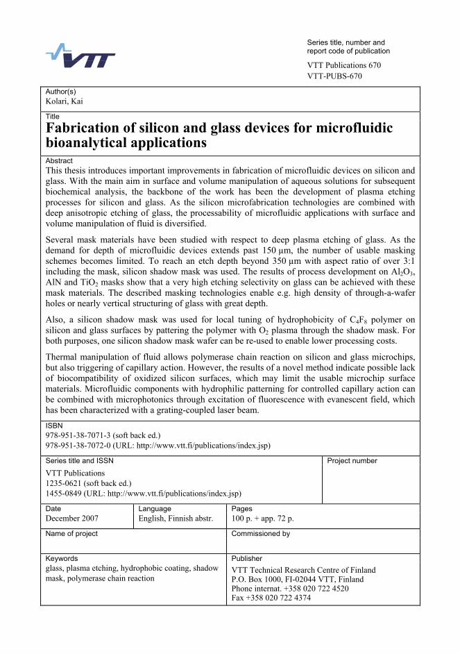
Series title, number and report code of publication
VTT Publications 670 VTT-PUBS-670
Author(s) Kolari, Kai
Title
Fabrication of silicon and glass devices for microfluidic bioanalytical applications Abstract This thesis introduces important improvements in fabrication of microfluidic devices on silicon and glass. With the main aim in surface and volume manipulation of aqueous solutions for subsequent biochemical analysis, the backbone of the work has been the development of plasma etching processes for silicon and glass. As the silicon microfabrication technologies are combined with deep anisotropic etching of glass, the processability of microfluidic applications with surface and volume manipulation of fluid is diversified.
Several mask materials have been studied with respect to deep plasma etching of glass. As the demand for depth of microfluidic devices extends past 150 µm, the number of usable masking schemes becomes limited. To reach an etch depth beyond 350 µm with aspect ratio of over 3:1 including the mask, silicon shadow mask was used. The results of process development on Al2O3, AlN and TiO2 masks show that a very high etching selectivity on glass can be achieved with these mask materials. The described masking technologies enable e.g. high density of through-a-wafer holes or nearly vertical structuring of glass with great depth.
Also, a silicon shadow mask was used for local tuning of hydrophobicity of C4F8 polymer on silicon and glass surfaces by pattering the polymer with O2 plasma through the shadow mask. For both purposes, one silicon shadow mask wafer can be re-used to enable lower processing costs.
Thermal manipulation of fluid allows polymerase chain reaction on silicon and glass microchips, but also triggering of capillary action. However, the results of a novel method indicate possible lack of biocompatibility of oxidized silicon surfaces, which may limit the usable microchip surface materials. Microfluidic components with hydrophilic patterning for controlled capillary action can be combined with microphotonics through excitation of fluorescence with evanescent field, which has been characterized with a grating-coupled laser beam.
ISBN 978-951-38-7071-3 (soft back ed.) 978-951-38-7072-0 (URL: http://www.vtt.fi/publications/index.jsp)
Series title and ISSN Project number
VTT Publications 1235-0621 (soft back ed.) 1455-0849 (URL: http://www.vtt.fi/publications/index.jsp)
Date Language Pages December 2007 English, Finnish abstr. 100 p. + app. 72 p.
Name of project Commissioned by
Keywords Publisher glass, plasma etching, hydrophobic coating, shadow mask, polymerase chain reaction
VTT Technical Research Centre of Finland P.O. Box 1000, FI-02044 VTT, Finland Phone internat. +358 020 722 4520 Fax +358 020 722 4374


Julkaisun sarja, numero ja raporttikoodi
VTT Publications 670 VTT-PUBS-670
Tekijä(t) Kolari, Kai
Nimeke
Pii- ja lasialustojen valmistaminen biomikrofluidistisiin sovelluksiin
Tiivistelmä Työssä käsitellään mikrofluidististen rakenteiden valmistamiseen liittyviä parannuksia. Työn tavoitteena on ollut nesteiden kaksi- ja kolmiulotteinen manipulointi, jonka ytimessä on plasma-syövytysprosessien kehitys piille ja lasille. Piin mikrovalmistusteknologioiden yhdistäminen lasin suurien syvyyksien anisotrooppiseen plasmasyövytykseen luo edellytyksiä uudentyyppisten mikro-fluidististen sovellusten valmistamiselle.
Lasin plasmasyövytykseen on sovellettu useita eri maskimateriaaleja. Pyrittäessä yli 150 µm:n plasmasyövytyssyvyyteen lasilla maskivaihtoehtojen lukumäärä on vähäinen. Pyrittäessä yli 350 µm syvyyteen ja yli 3:1 aspektisuhteeseen työssä on käytetty piivarjomaskia. Erityisesti alumiinioksidi- ja -alumiininitridimaskeilla voidaan saavuttaa hyvin suuri syöpymisnopeussuhde lasiin. Työssä kuvattuja maskiteknologioita voidaan käyttää mm. läpivientien sekä lähes pystysuorien ja erittäin syvien lasirakenteiden syövyttämiseen.
Piivarjomaskiteknologia soveltuu myös käytettäväksi paikallisten hydrofiilisten kuviointien valmistamiseen hydrofobiselle C4F8-plasmapolymeeripinnoitteelle O2-plasman avulla. Samaa varjo-maskia voidaan käyttää moneen kertaan, josta seuraa ilmeisiä aika- ja kustannussäästöjä.
Nesteiden lämpötilan muuttaminen mikrofluidistisilla alustoilla mahdollistaa mm. polymeraasi-ketjureaktion ja kapillaari-ilmiön voimakkuuden muuttamisen. Oksidoitujen piipintojen bioyhteen-sopivuus kuitenkin vaihtelee, minkä tutkimiseen on työssä käytetty uutta menetelmää. Nesteiden manipulointiin kykeneviä mikrofluidistisia rakenteita voidaan yhdistää fotoniikkaan esim. evanescent-kentän avulla, jota on tässä työssä karakterisoitu valmistamalla hiloja piinitridivalokanavaan, jonka päälle tuodaan fluoresoivia pisaroita.
ISBN 978-951-38-7071-3 (nid.) 978-951-38-7072-0 (URL: http://www.vtt.fi/publications/index.jsp)
Avainnimeke ja ISSN Projektinumero VTT Publications 1235-0621 (nid.) 1455-0849 (URL: http://www.vtt.fi/publications/index.jsp)
Julkaisuaika Kieli Sivuja Joulukuu 2007 Englanti, suom. tiiv. 100 s. + liitt. 72 s.
Projektin nimi Toimeksiantaja(t)
Avainsanat Julkaisija
glass, plasma etching, hydrophobic coating, shadow mask, polymerase chain reaction
VTT PL 1000, 02044 VTT Puh. 020 722 4404 Faksi 020 722 4374

VTT P
UB
LICA
TION
S 670 Fabrication of silicon and glass devices for m
icrofluidic bioanalytical applicationsK
olari
ESPOO 2007ESPOO 2007ESPOO 2007ESPOO 2007ESPOO 2007 VTT PUBLICATIONS 670
Kai Kolari
Fabrication of silicon and glass devicesfor microfluidic bioanalyticalapplications
VTT PUBLICATIONS
649 Niskanen, Ilkka. An interactive ontology visualization approach for the domain ofnetworked home environments. 2007. 112 p. + app. 19 p.
650 Wessberg, Nina. Teollisuuden häiriöpäästöjen hallinnan kehittämishaasteet. 2007.195 s. + liitt. 4 s.
651 Laitakari, Juhani. Dynamic context monitoring for adaptive and context-awareapplications. 2007. 111 p. + app. 8 p.
652 Wilhelmson, Annika. The importance of oxygen availability in two plant-basedbioprocesses: hairy root cultivation and malting. 2007. 66 p. + app. 56 p.
653 Ahlqvist, Toni, Carlsen, Henrik, Iversen, Jonas & Kristiansen, Ernst. Nordic ICTForesight. Futures of the ICT environment and applications on the Nordic level.2007. 147 p. + app. 24 p.
654 Arvas, Mikko. Comparative and functional genome analysis of fungi for developmentof the protein production host Trichoderma reesei. 100 p. + app. 105 p.
655 Kuisma, Veli Matti. Joustavan konepaja-automaation käyttöönoton onnistumisenedellytykset. 2007. 240 s. + liitt. 68 s.
656 Hybrid Media in Personal Management of Nutrition and Exercise. Report on theHyperFit Project. Ed. by Paula Järvinen. 121 p. + app. 2 p.
657 Szilvay, Géza R. Self-assembly of hydrophobin proteins from the fungus Trichode-rma reesei. 2007. 64 p. + app. 43 p.
658 Palviainen, Marko. Technique for dynamic composition of content and context-sensitive mobile applications. Adaptive mobile browsers as a case study. 2007.233 p.
659 Qu, Yang. System-level design and configuration management for run-time recon-figurable devices. 2007. 133 p.
660 Sihvonen, Markus. Adaptive personal service environment. 2007. 114 p. + app. 77 p.
661 Rautio, Jari. Development of rapid gene expression analysis and its application tobioprocess monitoring. 2007. 123 p. + app. 83 p.
662 Karjalainen, Sami. The characteristics of usable room temperature control. 2007.133 p. + app. 71 p.
663 Välkkynen, Pasi. Physical Selection in Ubiquitous Computing. 2007. 97 p. + app.96 p.
664 Paaso, Janne. Moisture depth profiling in paper using near-infrared spectroscopy.2007. 193 p. + app. 6 p.
666 Prunnila, Mika. Single and many-band effects in electron transport and energyrelaxation in semiconductors. 2007. 68 p. + app. 49 p.
670 Kolari, Kai. Fabrication of silicon and glass devices for microfluidic bioanalyticalapplications. 2007. 100 s. + liitt. 72 s.
ISBN 978-951-38-7071-3 (soft back ed.) ISBN 978-951-38-7072-0 (URL: http://www.vtt.fi/publications/index.jsp)ISSN 1235-0621 (soft back ed.) ISSN 1455-0849 (URL: http://www.vtt.fi/publications/index.jsp)
Julkaisu on saatavana Publikationen distribueras av This publication is available from
VTT VTT VTTPL 1000 PB 1000 P.O. Box 1000
02044 VTT 02044 VTT FI-02044 VTT, FinlandPuh. 020 722 4520 Tel. 020 722 4520 Phone internat. + 358 20 722 4520
http://www.vtt.fi http://www.vtt.fi http://www.vtt.fi