fabrication technology for double-gate field effect transistors · fabrication technology for...
TRANSCRIPT

Fabrication Technology for Double-Gate Field EffectTransistors
byAndrew P. Ritenour
Bachelor of Science in Electrical EngineeringUniversity of Virginia, May 1997
Submitted to theDepartment of Electrical Engineering and Computer Science
in partial fulfillment of the requirements for the degree of
Master of Sciencein Electrical Engineering and Computer Science
at theMassachusetts Institute of Technology
August 1999
@ MassachusettsTnstitute of Technolog'Y 1999.All rights reserved
AuthorDepartment o Electrical Enineering and Computer Science
August 1999
Certified byDimitri A. Antoniadis
Professor of Electrical EngineeringThesis Supervisor
Accepted byArthur C. Smith
Professor o lectrical EngineeringNtO Lth Graduate Officer

2
Fabrication Technology for Double-Gate Field Effect Transistors
by
Andrew P. Ritenour
Submitted to the Department of Electrical Engineering and Computer Science
on August 25, 1999
in partial fulfillment of the requirements for the degree of
Master of Science in Electrical Engineering and Computer Science
Abstract
It has been shown that the double-gate MOSFET can provide high current drive and goodelectrostatic integrity at gate lengths of 20-30 nm. The top and bottom gates should be perfectlyaligned to maximize current drive and to avoid introducing a varying overlap capacitancebetween the bottom gate and source/drain regions. Perfect alignment is best achieved throughself-alignment. Finding a process that takes advantage of self-alignment and is extendable tomainstream manufacturing and well suited for integration in the third dimension remains a keychallenge. This work proposes and demonstrates a novel self-alignment scheme for double-sided,double-gate MOSFETs that meets these requirements. The "double-sided" nature of these devicesmakes them particularly well suited for 3-D integration.
Thesis Supervisor: Dimitri A. AntoniadisTitle: Professor of Electrical Engineering
3

4

Acknowledgments
I would like to first acknowledge the support and guidance provided by my advisor, Dimitri
Antoniadis, and my student mentor, Andy Wei. I would also like to thank Mark Armstrong, Tony
Lochtefeld, Keith Jackson, Ihsan Djomehri, Hasan Nayfeh, Zachary Lee, Dr. Jong-Ho Lee, and
the entire MTL staff for all kinds of help.
I would also like to acknowledge the invaluable technical assistance provided by Andy Loomis at
the MIT Lincoln Laboratory. I would also like to thank Andy for the countless hours spent
thinning my wafers.
5

6
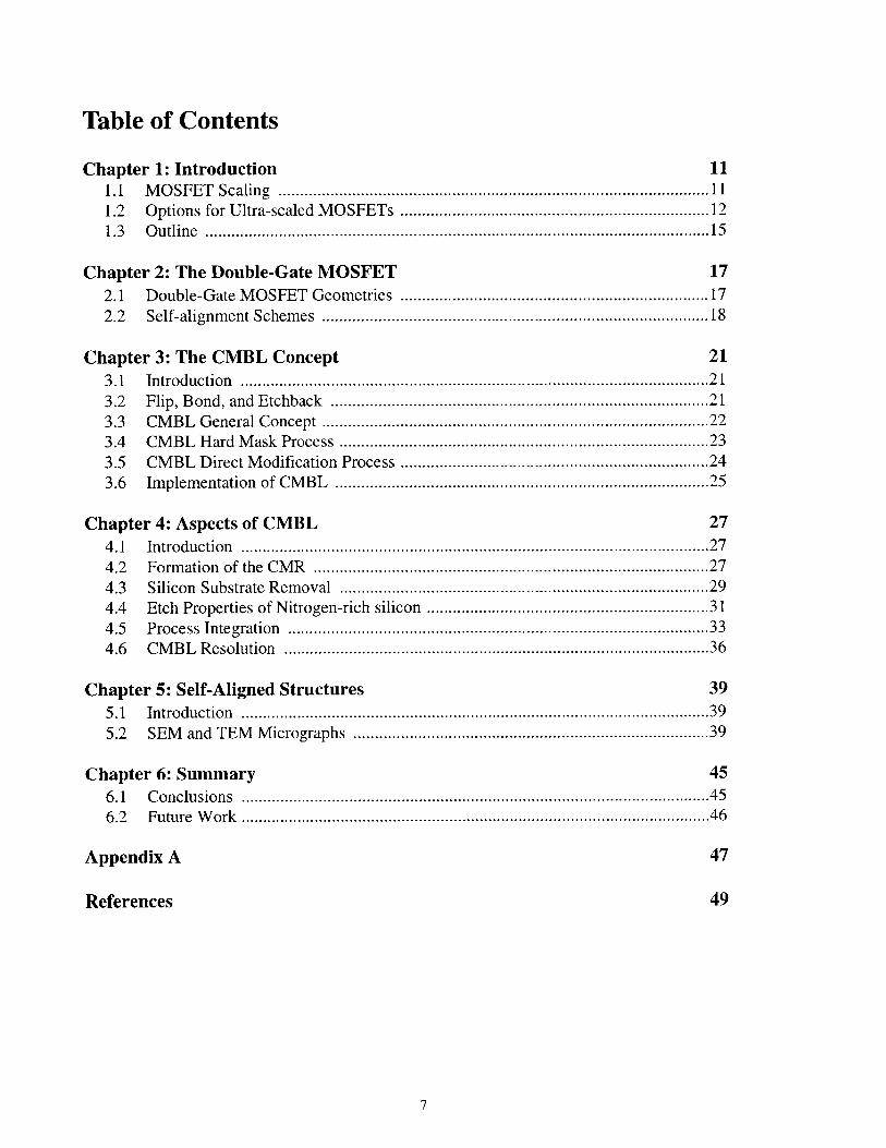
Table of Contents
Chapter 1: Introduction 111.1 M OSFET Scaling .............................................................................................. 111.2 Options for Ultra-scaled M OSFETs ................................................................... 121.3 Outline .................................................................................................................... 15
Chapter 2: The Double-Gate MOSFET 172.1 Double-Gate M OSFET Geom etries ................................................................... 172.2 Self-alignm ent Schem es ..................................................................................... 18
Chapter 3: The CMBL Concept 213.1 Introduction ........................................................................................................ 213.2 Flip, Bond, and Etchback ................................................................................... 213.3 CM BL General Concept ...................................................................................... 223.4 CM BL Hard M ask Process ................................................................................. 233.5 CM BL Direct M odification Process .................................................................... 243.6 Im plem entation of CM BL ................................................................................. 25
Chapter 4: Aspects of CMBL 274.1 Introduction ........................................................................................................ 274.2 Form ation of the CM R ........................................................................................ 274.3 Silicon Substrate Rem oval ................................................................................. 294.4 Etch Properties of Nitrogen-rich silicon ............................................................. 314.5 Process Integration ............................................................................................ 334.6 CM BL Resolution .............................................................................................. 36
Chapter 5: Self-Aligned Structures 395.1 Introduction ........................................................................................................ 395.2 SEM and TEM M icrographs .................................................................................. 39
Chapter 6: Summary 456.1 Conclusions ........................................................................................................ 456.2 Future W ork ........................................................................................................ 46
Appendix A 47
References 49
7

8

Table of Figures
Figure 1-1: Scaling of fully-depleted SOI MOSFETs [courtesy of Andy Wei, MIT] ............. 13
Figure 1-2: A schematic of a double-gate MOSFET ............................................................... 14
Figure 2-1: Double-gate MOSFET geometries ........................................................................ 17
Figure 2-2: Double-gate self-alignment schemes .................................................................... 19
Figure 3-1: Flip, bond, and etchback process for forming a buried gate ................................. 22
Figure 3-2: Schematic of the CMBL concept. The regions labeled B have been chemically
modified. The region labeled A was masked by the gate and thus remains unchanged .......... 23
Figure 3-3: Hard mask version of the CMBL process ............................................................. 23
Figure 3-4: Direct modification version of CMBL ................................................................. 24
Figure 3-5: Fabrication sequence for self-aligned double-gate MOSFETs using CMBL ..... 25
Figure 4-1: N itrogen diffusion in silicon ................................................................................. 28
Figure 4-2: Nitrogen profile after 1x 1017 cm 2 55 keV N 14 implant through 1000 A oxide and
sub sequent anneal ........................................................................................................................ 28
Figure 4-3: Implant conditions for TMAH selectivity tests .................................................. 29
Figure 4-4: Ratio of Si etch rate to nitrogen-implanted silicon etch rate in TMAH for different
im plant doses and energies ..................................................................................................... 30
Figure 4-5: Nitrogen bonding configurations .......................................................................... 31
Figure 4-6: The measured thickness of a -450A hard mask assuming the optical properties of
three materials: silicon, polysilicon, and silicon nitride. The measurements show that the
chemically modified regions are optically similar to silicon and polysilicon ......................... 32
Figure 4-7: A "gate shield" which could be used to protect the gate and gate dielectric from the
nitrogen im plant ........................................................................................................................... 34
Figure 4-8: Method for "reversing" a negative hard mask to form a positive hard mask ..... 35
Figure 4-9: An example of buried interconnect fabricated using the flip, bond, and etchback
approach [courtesy of Andy W ei, M IT] ................................................................................... 35
Figure 4-10: Effect of contrast on the relative sizes of the hard mask the implant mask (adapted
fro m [3 3 ]) ..................................................................................................................................... 3 6
Figure 5-1: Fabrication sequence for a self-aligned dummy gates .......................................... 40
9

Figure 5-2: SEM micrograph of self-aligned trench that was etched using the nitrogen-rich silicon
as a hard mask. The trench was filled with silicon nitride. A 1000 A oxide was used to simulate
the thin silicon and buried oxide of an SOI wafer ................................................................... 40
Figure 5-3: SEM micrograph of hard mask formed using CMBL process. A 1000 A oxide was
used to simulate the thin silicon and buried oxide of an SOI wafer. The hard mask is
approximately 600 A thick. It appears to be thicker because the top surface of the hard mask was
exposed during cross-section decoration ................................................................................ 41
Figure 5-4: Comparison between ideal and non-ideal implant masks. Ideally, the ion beam should
be perfectly collimated; however, this is not the case in real systems ..................................... 42
Figure 5-5: TEM micrograph of hard mask formed using CMBL .............................................. 43
10
Chapter 1
Introduction
1.1 MOSFET Scaling
Scaling the physical dimensions of metal-oxide-semiconductor field-effect transistors
(MOSFETs) [1] increases the drive current and reduces the areal size while maintaining low off-
state leakage current. Scaling the supply voltage (Vdd) reduces the dynamic power of the device.
These two scaling trends allow each new generation of integrated circuits (ICs) to achieve higher
performance and higher levels of integration than the previous generation.
As the physical dimensions of a MOSFET are scaled, the electrostatic integrity of the device must
be preserved. Electrostatic integrity provides immunity against short-channel effects, namely
threshold voltage roll-off and drain-induced barrier lowering (DIBL). In MOSFET scaling, the
gate length is scaled by 1/s where s is the scaling factor. To maintain the electrostatic integrity of
the device, the gate oxide thickness is scaled by 1/r where r is less than or equal to s. The source/
drain junction depth (in bulk MOSFETs) or silicon film thickness (in fully-depleted silicon-on-
insulator MOSFETs) are also scaled accordingly. Non-uniform doping profiles ("halo"s or
"pocket"s around the source/drain regions and a super-steep retrograde profile in the channel) can
also be used to suppress short-channel effects [2]. These scaling strategies have been effective in
the past, however, they will become ineffective or difficult to implement as MOSFETs reach sub-
100 nm dimensions. For example, the SIA roadmap calls for an equivalent gate oxide thickness of
11
less than 1.5 nm for the 70 nm generation. However, one estimate places the physical limit for
equivalent gate oxide thickness at 1.5 nm [3]. The SIA roadmap also calls for a minimum logic
Vdd of 0.6-0.9 V for the 70 nm generation. Simulations that consider process and circuit
variations, circuit operation temperature, and short channel effects indicate that the supply voltage
and threshold voltage have lower limits at 0.6 V and 0.3 V respectively [4]. These limits suggest
that oxide and supply voltage scaling will not be effective beyond the 70 nm generation. In order
to continue scaling, highly non-uniform doping profiles will be required to maintain good
electrostatic integrity and low off-current. These doping profiles are typically characterized by
peak concentrations greater than 1x10 18 cm- 3. High dopant concentrations in the body and
channel decrease the carrier mobility through impurity scattering and increase the parasitic
source/drain capacitance of the device. The threshold voltage variation introduced by statistical
dopant fluctuation may also be a concern for ultra-scaled MOSFETs [3].
1.2 Options for Ultra-scaled MOSFETs
Despite these apparent limitations, a bulk MOSFET with an effective channel length of 25 nm and
a "super-halo" doping profile has been proposed [3]. The "super-halo" produces a peak doping
concentration of 1x10 19 cm-3 in the body of the device and a doping concentration greater than
1x10 18 cm- 3 near the Si-Si0 2 interface. This doping profile has numerous consequences. The
low-field carrier mobility will be extremely low due to impurity scattering which will negate the
potential benefits of velocity overshoot. Band-to-band tunneling between the n++ drain and the
p+ halo may introduce excessive leakage. The lateral source/drain gradient must be steeper than
4-5 nm per decade for the device to have good electrostatic integrity. This requirement necessarily
places a limit on the thermal budget seen after the source/drain and halo implants. The super-halo
doping profile also dictates the use of n+/p+ polysilicon gates to achieve the proper threshold
voltage (-0.2-0.3 V). Polysilicon gate depletion reduces the current drive (IDSAT) by 10% on
average. The high peak doping concentration will also increase the parasitic source/drain-to-
substrate junction capacitance which will also negatively impact device performance. All of these
problems provide the motivation to search for alternatives to the bulk MOSFET for ultra-scaled
CMOS devices.
12
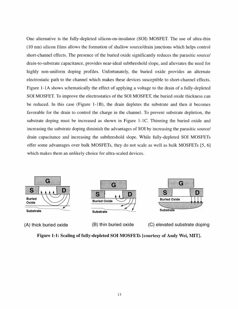
One alternative is the fully-depleted silicon-on-insulator (SOI) MOSFET. The use of ultra-thin
(10 nm) silicon films allows the formation of shallow source/drain junctions which helps control
short-channel effects. The presence of the buried oxide significantly reduces the parasitic source/
drain-to-substrate capacitance, provides near-ideal subthreshold slope, and alleviates the need for
highly non-uniform doping profiles. Unfortunately, the buried oxide provides an alternate
electrostatic path to the channel which makes these devices susceptible to short-channel effects.
Figure 1-1A shows schematically the effect of applying a voltage to the drain of a fully-depleted
SOI MOSFET. To improve the electrostatics of the SOI MOSFET, the buried oxide thickness can
be reduced. In this case (Figure 1-1B), the drain depletes the substrate and then it becomes
favorable for the drain to control the charge in the channel. To prevent substrate depletion, the
substrate doping must be increased as shown in Figure 1-1C. Thinning the buried oxide and
increasing the substrate doping diminish the advantages of SOI by increasing the parasitic source/
drain capacitance and increasing the subthreshold slope. While fully-depleted SOI MOSFETs
offer some advantages over bulk MOSFETs, they do not scale as well as bulk MOSFETs [5, 6]
which makes them an unlikely choice for ultra-scaled devices.
SEDBuried uidOdeBuried Oxide
Oxideu xide
Substrate - Substrate ..... Substrate
(A) thick buried oxide (B) thin buried oxide (C) elevated substrate doping
Figure 1-1: Scaling of fully-depleted S01 MOSFETs [courtesy of Andy Wei, MIT].
13
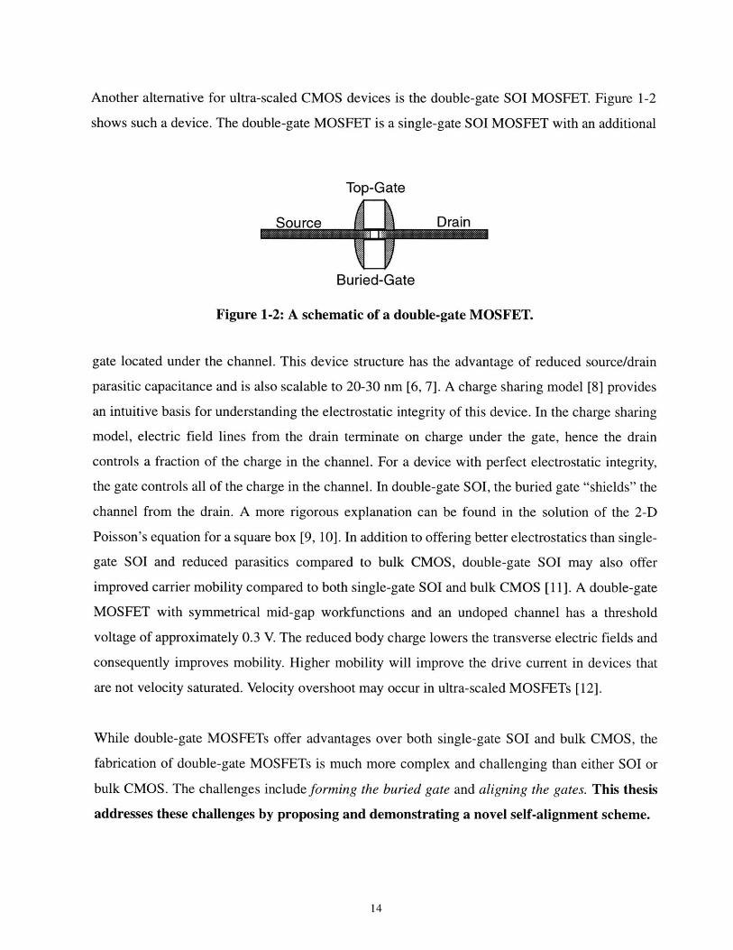
Another alternative for ultra-scaled CMOS devices is the double-gate SOI MOSFET. Figure 1-2
shows such a device. The double-gate MOSFET is a single-gate SOI MOSFET with an additional
Top-Gate
Source Drain
Buried-Gate
Figure 1-2: A schematic of a double-gate MOSFET.
gate located under the channel. This device structure has the advantage of reduced source/drain
parasitic capacitance and is also scalable to 20-30 nm [6, 7]. A charge sharing model [8] provides
an intuitive basis for understanding the electrostatic integrity of this device. In the charge sharing
model, electric field lines from the drain terminate on charge under the gate, hence the drain
controls a fraction of the charge in the channel. For a device with perfect electrostatic integrity,
the gate controls all of the charge in the channel. In double-gate SOI, the buried gate "shields" the
channel from the drain. A more rigorous explanation can be found in the solution of the 2-D
Poisson's equation for a square box [9, 10]. In addition to offering better electrostatics than single-
gate SOI and reduced parasitics compared to bulk CMOS, double-gate SOI may also offer
improved carrier mobility compared to both single-gate SOI and bulk CMOS [11]. A double-gate
MOSFET with symmetrical mid-gap workfunctions and an undoped channel has a threshold
voltage of approximately 0.3 V. The reduced body charge lowers the transverse electric fields and
consequently improves mobility. Higher mobility will improve the drive current in devices that
are not velocity saturated. Velocity overshoot may occur in ultra-scaled MOSFETs [12].
While double-gate MOSFETs offer advantages over both single-gate SOI and bulk CMOS, the
fabrication of double-gate MOSFETs is much more complex and challenging than either SOI or
bulk CMOS. The challenges include forming the buried gate and aligning the gates. This thesis
addresses these challenges by proposing and demonstrating a novel self-alignment scheme.
14

1.3 Outline
Chapter 2 reviews the double-gate fabrication schemes that have been reported to date in the
literature. Chapter 3 describes the new technique proposed in this work, chemical modification of
buried layers (CMBL). Chapter 4 discusses the various aspects of fabrication using CMBL
including process integration issues. Chapter 5 presents SEM and TEM micrographs of self-
aligned gates that have been fabricated using CMBL. Chapter 6 summarizes this work and
describes future work.
15

16

Chapter 2
The Double-Gate MOSFET
2.1 Double-Gate MOSFET Geometries
Many novel processes and device geometries have been proposed to address the challenges
associated with fabricating double-gate MOSFETs. Figure 2-1 shows possible double-gate
geometries. Figure 2-1A shows a planar double-gate MOSFET. Planar double gate MOSFETs
I
I
At 4Lt I
gate
(B) vertical pillar (C) vertical fin
Figure 2-1: Double-gate MOSFET geometries.
may be described as "symmetric" or "asymmetric." In symmetric devices, the two gates have the
same work-function, are equally sized, and have the same gate oxide thickness. Asymmetric
devices typically have an oversized back-gate, a thicker back-gate oxide, and front and back gates
17
source
(A) planar
drain
with different work functions. Symmetric double-gate MOSFETs are generally operated with the
two gates electrically connected. Asymmetric double-gate MOSFETS are generally operated with
independent control of the back-gate for variable Vt applications [13]. A planar double-gate
MOSFET with a gate that surrounds the channel (surround-gate) has also been reported [14].
Figure 2-1B shows a vertical pillar surround-gate MOSFET [15]. Figure 2-1C shows a vertical fin
double-gate MOSFET. The vertical fin is best suited for surround-gate devices [16]. In both
planar and vertical devices, surround-gates are used to avoid the problems associated with
aligning two separate gates.
2.2 Self-alignment Schemes
To date four self-alignment schemes have been proposed:
- direct-alignment (planar)
* surround-gate (planar and vertical)
- transparent substrate (planar)
- simultaneous gate definition (planar)
Direct Alignment
Direct alignment can be used to align the top-gate to a pre-existing buried gate. For a double-gate
MOSFET with a drawn gate length (LG) of 50 nm and an alignment tolerance of LG/4 [17], any
direct alignment scheme must have an alignment tolerance better than 12.5 nm. Under ideal
conditions, misalignments of 10 nm can be detected; however, detecting and correcting
misalignments of this order in a manufacturing environment will be challenging [18]
Surround-gate
The surround-gate approach eliminates the alignment requirement by using a gate that surrounds
the channel rather than two distinct gates on either side of the channel. The surround-gate
18

approach is often used in conjunction with vertical pillars or fins and less frequently with planar
devices. Vertical devices, however, have their own set of problems. The lithographic capability
required to pattern the ultra-thin (10 nm) silicon films (or pillars) used in ultra-scaled double-gate
MOSFETs must be "at least four times more stringent than the minimum gate length [19]." An
attempt to incorporate a surround-gate into a planar double-gate MOSFET [19] yielded a
complicated, non-manufacturable process in which tunnel epitaxy is used to form a suspended
silicon channel.
Transparent Substrate
A self-alignment scheme that takes advantage of a transparent substrate has been reported [20].
Figure 2-2A shows the process. A buried gate is formed beneath the silicon device layer. These
photoresist
LTO silica
quart su gate
quartz substrate
photons
gate stack
n device layer
(A) transparent substrate (B) simultaneous gate definition
Figure 2-2: Double-gate self-alignment schemes.
layers are bonded to a quartz wafer using LTO. A gate stack consisting of a gate dielectric and a
gate material is formed on the top surface of the silicon device layer. Photoresist is applied to the
wafer, and exposed using the buried gate as a mask. The photoresist is then used as a mask for
19
etching a gate that is self-aligned to the buried gate. This approach has several problems. First,
using optical pattern transfer when the length of the buried gate is 50 nm will be difficult, if not
impossible, and second, quartz wafers are difficult to work with in manufacturing environment
because they are more fragile than silicon wafers.
Simultaneous Gate Definition
In simultaneous gate definition, wafer bonding is used to form a wafer with the following layer
structure: gate material - thin gate dielectric - thin silicon film - thin gate dielectric - gate material
- and insulating film all on a silicon substrate. A fin like the one shown in Figure 2-2B is then
etched. Etching both gates at the same produces self-aligned gates, however, the source and drain
regions have also been etched away. The source and drain regions can be regrown using selective
epitaxy [21]. IBM has proposed another scheme for forming the source/drain regions on such a
device [22]. In either case, providing source and drain terminals for these devices remains a
challenge.
None of these four techniques have yet been proven the best solution for double-gate MOSFET
fabrication. All have serious issues that remain unresolved. The next chapter describes the novel
self-alignment scheme being proposed in this work.
20
Chapter 3
The CMBL Concept
3.1 Introduction
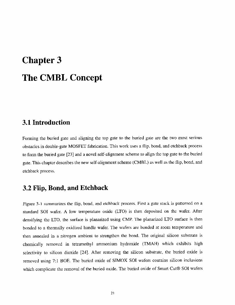
Forming the buried gate and aligning the top gate to the buried gate are the two most serious
obstacles in double-gate MOSFET fabrication. This work uses a flip, bond, and etchback process
to form the buried gate [23] and a novel self-alignment scheme to align the top gate to the buried
gate. This chapter describes the new self-alignment scheme (CMBL) as well as the flip, bond, and
etchback process.
3.2 Flip, Bond, and Etchback
Figure 3-1 summarizes the flip, bond, and etchback process. First a gate stack is patterned on a
standard SOI wafer. A low temperature oxide (LTO) is then deposited on the wafer. After
densifying the LTO, the surface is planarized using CMP. The planarized LTO surface is then
bonded to a thermally oxidized handle wafer. The wafers are bonded at room temperature and
then annealed in a nitrogen ambient to strengthen the bond. The original silicon substrate is
chemically removed in tetramethyl ammonium hydroxide (TMAH) which exhibits high
selectivity to silicon dioxide [24]. After removing the silicon substrate, the buried oxide is
removed using 7:1 BOE. The buried oxide of SIMOX SOI wafers contains silicon inclusions
which complicate the removal of the buried oxide. The buried oxide of Smart Cut@ SOI wafers
21
does not contain silicon inclusions. Appendix A contains a detailed process flow including
machine names, recipe numbers, and CMP parameters.
(A) Form gate stack on SOIwafer.
m" .,polysilicon
/gate oxide-silicon
buried oxide
silicon substrate
(B) Deposit LTO and planarizeusing CMP.
LTo
silicon substrate
(C) Flip and bond to handlewafer.
(D) Remove silicon substrate andburied oxide.
S ,,BondedInterface
Handle Wafer
Figure 3-1: Flip, bond, and etchback process for forming a buried gate.
The self-alignment scheme proposed in this work is designed to be used in conjunction with the
flip, bond, and etchback process. The scheme relies on the chemical modification of buried layers
(CMBL).
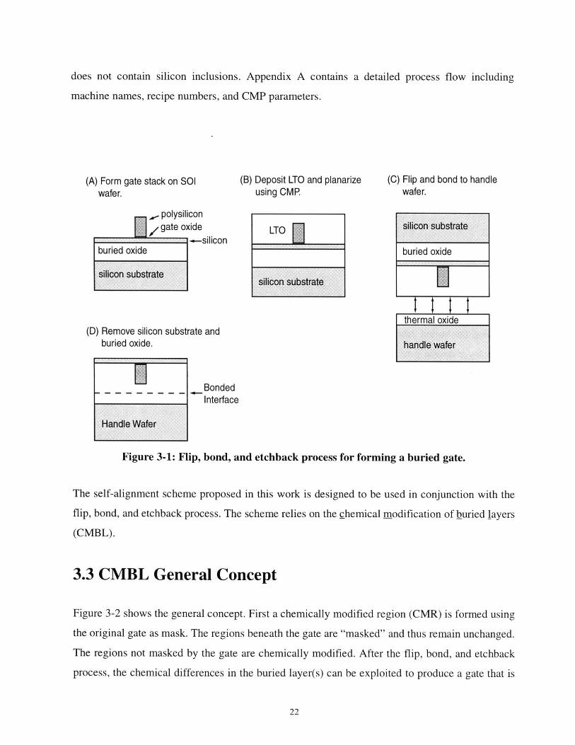
3.3 CMBL General Concept
Figure 3-2 shows the general concept. First a chemically modified region (CMR) is formed using
the original gate as mask. The regions beneath the gate are "masked" and thus remain unchanged.
The regions not masked by the gate are chemically modified. After the flip, bond, and etchback
process, the chemical differences in the buried layer(s) can be exploited to produce a gate that is
22

self-aligned to the buried gate. The next two sections discuss two specific implementations of the
CMBL process. The first involves using the CMR as a hard mask and the second involves directly
modifying the layer of interest.
device layer
buried layer
buried layer(substrate)
gate
(A) Before flip, bond, and etchback (B) After flip, bond, and etchback
Figure 3-2: Schematic of the CMBL concept. The regions labeled B have been chemicallymodified. The region labeled A was masked by the gate and thus remains unchanged.
3.4 CMBL Hard Mask Process
In the hard mask version of CMBL, a hard mask formed in one buried layer is used to etch another
buried layer. Figure 3-3 shows an example of a hard mask process. In Figure 3-3A, the silicon
positive hard mask positive hard mask
S pilA "'M M
negative hard mask negative hard mask
(A) Chemical modification (B) Flip, bond, and etchback (C) Etching with the hard mask
Figure 3-3: Hard mask version of the CMBL process.
23
gate/ 'Si
SOI
CMR
B A B

region just beneath the buried oxide is chemically modified. During the flip, bond, and etchback
process, TMAH is used to remove the original silicon substrate. If the chemically modified silicon
regions etch more slowly than silicon, a negative "hard mask" will remain as shown in Figure 3-
3B. If the opposite is true, a positive hard mask will remain. The negative hard mask can be used
to etch a trench that is self-aligned to the buried gate. Using a damascene process, a gate may be
formed in the self-aligned trench. The positive hard mask may be used to etch an oxide fin that is
self-aligned to the buried gate. This "dummy" gate may be replaced with a real gate using a
replacement gate process [25]. If the original wafer had blanket gate material and gate dielectric
films buried beneath the channel instead of a buried oxide, the positive hard mask process would
produce a self-aligned gate rather than a self-aligned dummy gate.
3.5 CMBL Direct Modification Process
In this version of CMBL, the layer of interest is directly modified. In figure 3-4, the buried oxide
layer itself is chemically modified. After the flip, bond, and etchback process, the buried oxide is
BOX B A BSoIl
CMR
(A) Chemical modification
B A: B
positive process
B A B
negative process
(B) Flip, bond, and etchback
A
positive process
negative process
(C) Etching the buried oxide
Figure 3-4: Direct modification version of CMBL.
exposed. In Figure 3-4C, the buried oxide is etched using a chemistry that etches the chemically
modified regions either slower than the unmodified regions (a negative process) or faster than the
unmodified regions (a positive process).
24

3.6 Implementation of CMBL
Figure 3-5 shows the CMBL process implemented in this work.
(1) Form gate stack on SOl wafer.
I -silicon
(4) Thin silicon substrate to 10pm. Exposenitrogen-rich silicon using TMAH.
(2) Implant nitrogen using polysilicongate as mask.
-nitrogen-richsilicon
(5) Etch self-aligned "trench" usingnitrogen-rich silicon as hard mask.
(3) Deposit oxide and planarize.Fli and bond to handle wafer.
(6) Form gate stack and removeexcess material using CMP
I M I I
- 11-Handle Wafer
BondedInterface
Figure 3-5: Fabrication sequence for self-aligned double-gate MOSFETs using CMBL.
It is a negative hard mask process in which a nitrogen implant is used to form a nitrogen-rich
silicon region just beneath the buried oxide-substrate interface.
The next chapter examines many aspects of this process including the formation, composition,
stability, and TMAH etch resistance of the chemically modified region as well as the pattern
transfer capability of the process.
25
--- M_

26

Chapter 4
Aspects of CMBL
4.1 Introduction
This chapter will examine each important step in the CMBL process and discuss process related
issues. The CMBL process described in Section 3.6 has three important steps:
- formation of the nitrogen-rich silicon region
- selective removal of the silicon substrate to expose the nitrogen-rich silicon
- etching of a self-aligned trench using the nitrogen-rich silicon as a hard mask
4.2 Formation of the CMR
A high dose nitrogen implant (6x10 16-1x10 1 7 cm-2) is used to form the nitrogen-rich silicon
region. The stability of the implanted nitrogen is an important issue. The lateral diffusion of
nitrogen during the bonding anneal could cause the hard mask edge to encroach under the edge of
the masking gate. The diffusion data in Figure 4-1 shows that nitrogen diffuses moderately faster
than boron at 850 'C. Fast diffusers are typically characterized by an activation energy (Ea in the
Arrhenius equation) of 0.2-2 eV while substitutional impurities (B, P, As) have an Ea of 3-4 eV
[26].
27
Species DO(cm 2/s) Ea(eV) D850 c(cm 2/s)
N [27] 0.87 3.29 1.62 x 10⁻¹⁵
N [27] 0.03 2.63 5.03 x 10⁻¹⁴
B [26] 0.76 3.46 2.45 x 10⁻¹⁶
Figure 4-1: Nitrogen diffusion in silicon.
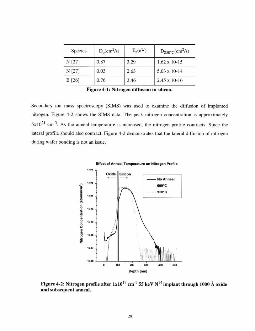
Secondary ion mass spectroscopy (SIMS) was used to examine the diffusion of implanted
nitrogen. Figure 4-2 shows the SIMS data. The peak nitrogen concentration is approximately
5x10 2 1 cm-3. As the anneal temperature is increased, the nitrogen profile contracts. Since the
lateral profile should also contract, Figure 4-2 demonstrates that the lateral diffusion of nitrogen
during wafer bonding is not an issue.
Effect of Anneal Temperature on Nitrogen Profile
1E23-.
E
E0
0U
0'U
C0
z
1E22
I E21
IE20
IE19
IE18
IE17
IE160 100 200 300
Depth (nm)
400 500
Figure 4-2: Nitrogen profile afterand subsequent anneal.
1x10 1 7 cm-2 55 keV N14 implant through 1000 A oxide
28
4.3 Silicon Substrate Removal
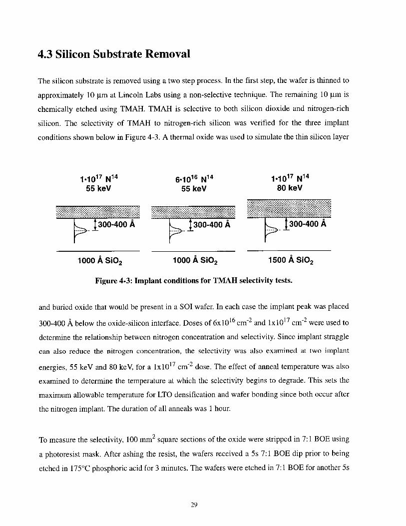
The silicon substrate is removed using a two step process. In the first step, the wafer is thinned to
approximately 10 gm at Lincoln Labs using a non-selective technique. The remaining 10 gm is
chemically etched using TMAH. TMAH is selective to both silicon dioxide and nitrogen-rich
silicon. The selectivity of TMAH to nitrogen-rich silicon was verified for the three implant
conditions shown below in Figure 4-3. A thermal oxide was used to simulate the thin silicon layer
1.1017 N14 6-1016 N14 1-1o 7 N1455 keV 55 keV 80 keV
300-400 A 300-400 A 300-400 A
1000 A SiO 2 1000 A SiO 2 1500 A SiO 2
Figure 4-3: Implant conditions for TMAH selectivity tests.
and buried oxide that would be present in a SOI wafer. In each case the implant peak was placed
300-400 A below the oxide-silicon interface. Doses of 6x1016 cm 2 and 1x1O17 cm-2 were used to
determine the relationship between nitrogen concentration and selectivity. Since implant straggle
can also reduce the nitrogen concentration, the selectivity was also examined at two implant
energies, 55 keV and 80 keV, for a 1x10 17 cm~2 dose. The effect of anneal temperature was also
examined to determine the temperature at which the selectivity begins to degrade. This sets the
maximum allowable temperature for LTO densification and wafer bonding since both occur after
the nitrogen implant. The duration of all anneals was 1 hour.
To measure the selectivity, 100 mm2 square sections of the oxide were stripped in 7:1 BOE using
a photoresist mask. After ashing the resist, the wafers received a 5s 7:1 BOE dip prior to being
etched in 175'C phosphoric acid for 3 minutes. The wafers were etched in 7:1 BOE for another 5s
29

immediately before being transferred to the 750C TMAH bath. This sequence of etches was
designed to remove any thin oxynitride or silicon nitride films that may have formed at the oxide-
silicon interface. TMAH is highly selective to silicon dioxide and silicon nitride so the presence
of a thin film at the surface would confuse the bulk selectivity measurement. Figure 4-4 shows the
measured data. The data shows that the selectivity increases up to 800'C and then decreases
Selectivity of TMAH to N"1'-Si
100 - 126171lxlO /55keV
mU...... 22
0
Ix 0 200 400 600 g00 1000
Anneal Temperature (*C)
Figure 4-4: Ratio of Si etch rate to nitrogen-implanted silicon etch rate in TMA H fordifferent implant doses and energies.
rapidly. The selectivity also appears to decrease rapidly for a moderate decrease in nitrogen
concentration. For a 1.7X reduction in dose the selectivity decreases by 5.7X. This sharp contrast
will help produce a hard mask with an abrupt edge. For a 1X1017 cm-2 dose, the reduction in
nitrogen concentration due to increased straggle at 80 keV reduces the selectivity by 50%. The
finite selectivity observed in these experiments places severe requirements on the wafer thinning
process. For a Si-to-N 14Si selectivity of 100, the thin (~10 ptm) silicon region being etched in
TMAH should have a maximum non-uniformity less than 2.5 tm. If the thin silicon region is not
uniform, some areas of the wafer will clear first and the TMAH will begin to slowly etch the
exposed hard mask. The maximum non-uniformity value was calculated assuming that the hard
mask will not function as a mask if its thickness is reduced by more than 250 A.
30
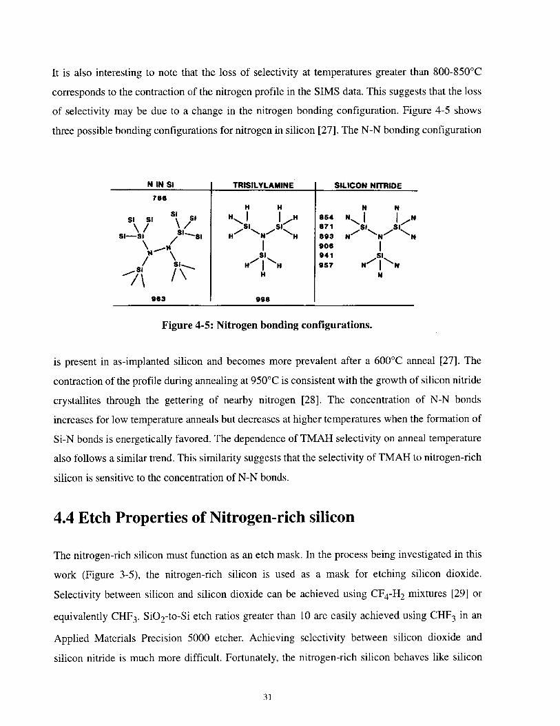
It is also interesting to note that the loss of selectivity at temperatures greater than 800-850'C
corresponds to the contraction of the nitrogen profile in the SIMS data. This suggests that the loss
of selectivity may be due to a change in the nitrogen bonding configuration. Figure 4-5 shows
three possible bonding configurations for nitrogen in silicon [27]. The N-N bonding configuration
N IN SI TRISILYLAMINE SILICON NITRIDE766
H H N N
SI SI SI H"" H 854 N N\/S1 S1 871 N5 1 SSi-S H N H 893 N N N
\ 906 |SI 941
se H |H 957 N N
|\ H N
963 998
Figure 4-5: Nitrogen bonding configurations.
is present in as-implanted silicon and becomes more prevalent after a 600'C anneal [27]. The
contraction of the profile during annealing at 950'C is consistent with the growth of silicon nitride
crystallites through the gettering of nearby nitrogen [28]. The concentration of N-N bonds
increases for low temperature anneals but decreases at higher temperatures when the formation of
Si-N bonds is energetically favored. The dependence of TMAH selectivity on anneal temperature
also follows a similar trend. This similarity suggests that the selectivity of TMAH to nitrogen-rich
silicon is sensitive to the concentration of N-N bonds.
4.4 Etch Properties of Nitrogen-rich silicon
The nitrogen-rich silicon must function as an etch mask. In the process being investigated in this
work (Figure 3-5), the nitrogen-rich silicon is used as a mask for etching silicon dioxide.
Selectivity between silicon and silicon dioxide can be achieved using CF 4-H2 mixtures [29] or
equivalently CHF 3. Si0 2-to-Si etch ratios greater than 10 are easily achieved using CHF3 in an
Applied Materials Precision 5000 etcher. Achieving selectivity between silicon dioxide and
silicon nitride is much more difficult. Fortunately, the nitrogen-rich silicon behaves like silicon
31
rather than silicon nitride in CHF 3 plasmas. Experimental evidence shows that the etch rate of
nitrogen-rich silicon in CHF 3 is small which is consistent with behavior of silicon. In this
experiment, the nitrogen-rich silicon served as a hard mask for etching a 700 A trench in thermal
oxide. The SiO 2 etch rate in CHF3 (RF power=350 W, CHF 3 flow rate=40 sccm, pressure=25 T,
magnetic field=75 gauss) was calibrated using a patterned amorphous silicon hard mask deposited
on 1000 A SiO2 . The wafer with the nitrogen-rich silicon hard mask was etched for 21 s for an
SiO 2 etch target of 735 A. After etching the sample, the step height (hole depth) was 1126 A.
Assuming that 735 A of SiO 2 was etched, the final hard mask thickness was 391 A. The initial
hard mask thickness was 434 A. Using these numbers, the ratio of the SiO2 etch rate to the
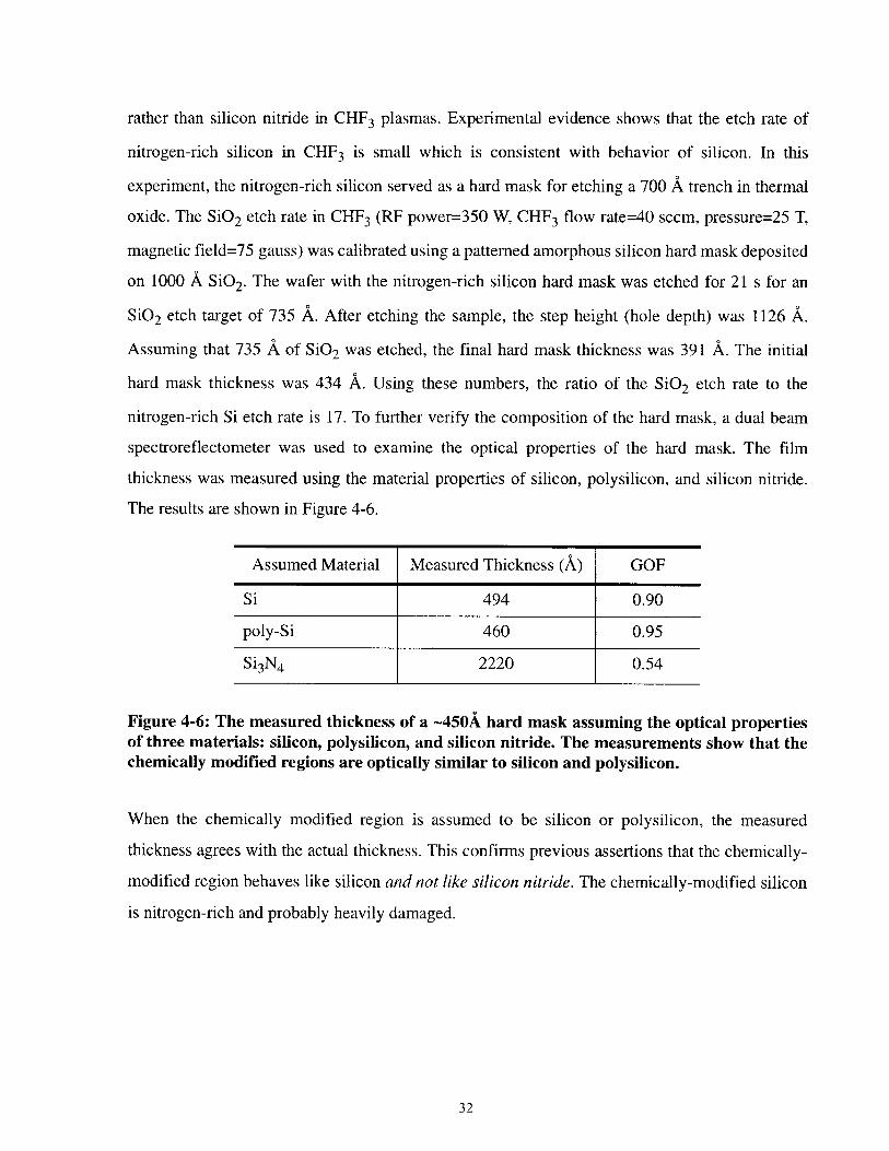
nitrogen-rich Si etch rate is 17. To further verify the composition of the hard mask, a dual beam
spectroreflectometer was used to examine the optical properties of the hard mask. The film
thickness was measured using the material properties of silicon, polysilicon, and silicon nitride.
The results are shown in Figure 4-6.
Assumed Material Measured Thickness (A) GOF
Si 494 0.90
poly-Si 460 0.95
Si 3N4 2220 0.54
Figure 4-6: The measured thickness of a -450A hard mask assuming the optical propertiesof three materials: silicon, polysilicon, and silicon nitride. The measurements show that thechemically modified regions are optically similar to silicon and polysilicon.
When the chemically modified region is assumed to be silicon or polysilicon, the measured
thickness agrees with the actual thickness. This confirms previous assertions that the chemically-
modified region behaves like silicon and not like silicon nitride. The chemically-modified silicon
is nitrogen-rich and probably heavily damaged.
32

4.5 Process Integration
Sections 4.2, 4.3, and 4.4 demonstrate that a chemically modified region can be exploited to form
a hard mask with suitable etch resistance. The usefulness of the process; however, will be partly
determined by its potential for integration into a manufacturable CMOS process. The primary
integration issues include the following:
- suitability of the flip, bond, and etchback process for manufacturing
- side-effects of the nitrogen implant process
- complications introduced by using a negative pattern transfer process.
The flip, bond, and etchback process would introduce several new processes into the
manufacturing environment. Wafer bonding is the primary concern because of the potential for
yield loss. Bonding patterned features is even more problematic because the topology must be
eliminated prior to bonding. The best known solution is chemical mechanical planarization
(CMP) which has severe pattern dependencies [30] that can lead to the formation of voids during
wafer bonding. In its current implementation, the flip, bond, and etchback process also requires a
wafer thinning process that is significantly more advanced than any wafer thinning process
currently used in production. The finite selectivity of TMAH to nitrogen-rich silicon places strict
uniformity requirements on the wafer thinning process. The original silicon substrate should be
thinned to 10 gm ± 1.25 pm which could be challenging for a 300 mm wafer.
The side-effects of the nitrogen implant process could be severe. The high implant dose will
inevitably damage the source/drain regions. Subsequent annealing may not be sufficient to repair
the damage. The literature suggests that nitrogen incorporation into the silicon substrate can
increase the parasitic source/drain resistance in p-MOSFETs [31]. The high dose will also damage
the gate dielectric near the gate edge possibly providing a gate to source/drain leakage path. Since
the gate is being used as a mask, the gate will also be subjected to a high dose of nitrogen which
may affect the electrical properties of the gate and sputter the top surface and edges. Figure 4-7
33
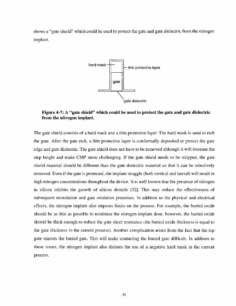
shows a "gate shield" which could be used to protect the gate and gate dielectric from the nitrogen
implant.
hard mask -thin protective layer
gate
gate dielectric
Figure 4-7: A "gate shield" which could be used to protect the gate and gate dielectricfrom the nitrogen implant.
The gate shield consists of a hard mask and a thin protective layer. The hard mask is used to etch
the gate. After the gate etch, a thin protective layer is conformally deposited to protect the gate
edge and gate dielectric. The gate shield does not have to be removed although it will increase the
step height and make CMP more challenging. If the gate shield needs to be stripped, the gate
shield material should be different than the gate dielectric material so that it can be selectively
removed. Even if the gate is protected, the implant straggle (both vertical and lateral) will result in
high nitrogen concentrations throughout the device. It is well known that the presence of nitrogen
in silicon inhibits the growth of silicon dioxide [32]. This may reduce the effectiveness of
subsequent reoxidation and gate oxidation processes. In addition to the physical and electrical
effects, the nitrogen implant also imposes limits on the process. For example, the buried oxide
should be as thin as possible to minimize the nitrogen implant dose; however, the buried oxide
should be thick enough to reduce the gate sheet resistance (the buried oxide thickness is equal to
the gate thickness in the current process). Another complication arises from the fact that the top
gate mirrors the buried gate. This will make contacting the buried gate difficult. In addition to
these issues, the nitrogen implant also dictates the use of a negative hard mask in the current
process.
34

The negative hard mask/replacement gate process poses several challenges. The nitrogen-rich
silicon forms a negative mask which is used to etch a self-aligned hole. The hole must be etched
without damaging the underlying silicon surface. The excess gate must also be removed which
forces CMP into the front-end of the process. After CMP, the source and drain regions will be
covered by the buried oxide. The buried oxide will need to be removed if the source and drain
regions were not silicided before the flip, bond, and etchback process. This oxide must be
removed without etching the gate oxide or isolation (when using a negative hard mask, the
isolation must be formed before the flip, bond, and etchback operation). It should be noted that the
negative hard mask can be reversed to form a positive hard mask as shown in Figure 4-8.
new mask material
buried oxide
(A) deposit new mask material (B) remove excess gate material (C) selectively remove original hardusing CMP mask
Figure 4-8: Method for "reversing" a negative hard mask to form a positive hard mask.
In addition to the challenges mentioned thus far, the process does have advantages from a process
integration standpoint. The process is compatible with metal gate technology and deposited gate
dielectrics. The flip, bond, and etchback process allows certain processes such as source/drain
implants and salicide to occur before or after the bonding step. And most importantly, the process
lends itself to 3-D integration. This process allows for buried interconnect and source/drain
connections on both sides of the device (Figure 4-9), hence the devices would be "double-sided."
}TopInterconnectLayer
Device(5( 09Layer
}BottomInterconnectLayer
Figure 4-9: An example of buried interconnect fabricated using the flip, bond, andetchback approach [courtesy of Andy Wei, MIT].
35
1111MiRM 1m =.Me171n.nIn

4.6 CMBL Resolution
The process integration issues discussed in the previous section become irrelevant if CMBL is not
capable of producing ultra-scaled self-aligned gates. The size of the hard mask opening is
determined by the as-implanted nitrogen profile near the mask edge, the diffusion of nitrogen
during the bonding thermal budget, and the contrast of the process. The "contrast" refers to the
relationship between the TMAH selectivity and the nitrogen concentration. In the case of "ideal"
contrast, the TMAH selectivity would instantaneously drop to zero at some critical nitrogen
concentration Nc. Figure 4-10 shows the lateral nitrogen profile at the edge of an implant mask.
mask
N(y)
1.0 No
0.5 No
(D I
ci~ yNc = 1.0 No
ENc = 0.5 No
Nc = 0.3 No
N(y) = nitrogen concentration along the y-direction at a fixed depth xNo = peak nitrogen concentrationNc = nitrogen concentration at which TMAH selectivity decreases to 1/2
of its maximum value (for high contrast, _ )0 .
NC
Figure 4-10: Effect of contrast on the relative sizes of the hard mask and implant mask(adapted from [33]).
36
No is the nitrogen concentration far away from the mask edge. The concentration decreases to
0.5NO at the mask edge and continues to decay under the mask edge according to the
complementary error function [33]. Figure 4-10 also shows the relationship between Nc and the
hard mask size. As long as Nc is greater than 0.5NO, the hard mask opening will be oversized
relative to the gate. If the hard mask opening is undersized compared to the gate mask by AL,
then the two edges of the hard mask will join when the gate mask has a drawn length of 2AL. For
a drawn gate length of 50nm, the nitrogen-rich silicon would become a continuous layer for AL =
25 nm. So, in order for CMBL to be useful, the hard mask opening must be the same size or
oversized relative to the gate mask. An oversized hard mask can be accurately corrected by
forming well-controlled silicon spacers on the hard mask edge prior to etching the hole or by
forming oxide spacers in the oversized hole. The next chapter shows SEM and TEM micrographs
of hard masks that have been fabricated using CMBL. In all cases, the hard mask is oversized
relative to the gate mask. This result agrees with the theory presented thus far. The TMAH data
shows that the selectivity drops by nearly 6X for a 1.7X reduction in dose. Given that the nitrogen
concentration at the edge of the mask is 2X lower than the concentration in the field, the TMAH
selectivity of the silicon at the edge of the mask is significantly reduced compared to the field.
This leads to an oversized hard mask.
37

38

Chapter 5
Self-Aligned Structures
5.1 Introduction
Self-aligned hard masks have been formed using the CMBL process described in Chapters 3 and
4. This chapter presents and discusses two SEM micrographs and one TEM micrograph of these
structures.
5.2 SEM and TEM Micrographs
Figure 5-1 shows the process used to fabricate the structure. First a polysilicon "gate" is patterned
on a p-type wafer with a 1000 A thermal oxide. The thermal oxide simulates the thin silicon and
buried oxide of an SOI wafer. The energy of the nitrogen implant was 55 keV. The projected range
for this implant is approximately 1400 A. The dose was 1x10 17 ions/cm-2 . The implant was
performed in five increments of 2x10¹⁶ ions/cm-2 . The wafers were allowed to cool between each
of the five implants. After the flip, bond, and etchback process, the hard mask was used to etch a
self-aligned trench in a CHF3 plasma. In the final step, the self-aligned trench is filled with silicon
nitride. The SEM micrograph of this structure is shown in Figure 5-2.
39

(1) Grow 1000 A oxide on wafer.Deposit and pattern 1200 Apolysilicon.
R polysilicon
1000 A thermal oxide
silicon substrate
(4) Thin silicon substrate to 10pm. Exposenitrogen-rich silicon using TMAH.
- - -- BondedInterface
(2) Implant nitrogen using polysilicongate as mask.
nitrogen-rich
siflicon substrate silicon
(5) Etch 750 A self-aligned "trench" usingnitrogen-rich silicon as hard mask.
(3) Deposit oxide and planarize.Flip and bond to handle wafer.
silicon substrate
LTO
thermal oxide
hanle wafer
(6) Fill self-aligned trench with siliconnitride.
silicon nitride
Handle Wafer
Figure 5-1: Fabrication sequence for self-aligned dummy gates.
3±1000 A
Figure 5-2: SEM micrograph of self-aligned trench that was etched using the nitrogen-richsilicon as a hard mask. The trench was filled with silicon nitride. A 1000 A oxide was used tosimulate the thin silicon and buried oxide of an SOI wafer.
40
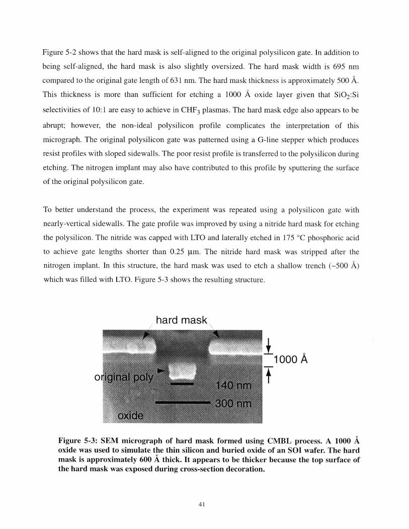
Figure 5-2 shows that the hard mask is self-aligned to the original polysilicon gate. In addition to
being self-aligned, the hard mask is also slightly oversized. The hard mask width is 695 nm
compared to the original gate length of 631 nm. The hard mask thickness is approximately 500 A.
This thickness is more than sufficient for etching a 1000 A oxide layer given that SiO 2 :Si
selectivities of 10:1 are easy to achieve in CHF3 plasmas. The hard mask edge also appears to be
abrupt; however, the non-ideal polysilicon profile complicates the interpretation of this
micrograph. The original polysilicon gate was patterned using a G-line stepper which produces
resist profiles with sloped sidewalls. The poor resist profile is transferred to the polysilicon during
etching. The nitrogen implant may also have contributed to this profile by sputtering the surface
of the original polysilicon gate.
To better understand the process, the experiment was repeated using a polysilicon gate with
nearly-vertical sidewalls. The gate profile was improved by using a nitride hard mask for etching
the polysilicon. The nitride was capped with LTO and laterally etched in 175 'C phosphoric acid
to achieve gate lengths shorter than 0.25 jim. The nitride hard mask was stripped after the
nitrogen implant. In this structure, the hard mask was used to etch a shallow trench (-500 A)
which was filled with LTO. Figure 5-3 shows the resulting structure.
hard mask
1000 A
Figure 5-3: SEM micrograph of hard mask formed using CMBL process. A 1000 Aoxide was used to simulate the thin silicon and buried oxide of an SOI wafer. The hardmask is approximately 600 A thick. It appears to be thicker because the top surface ofthe hard mask was exposed during cross-section decoration.
41
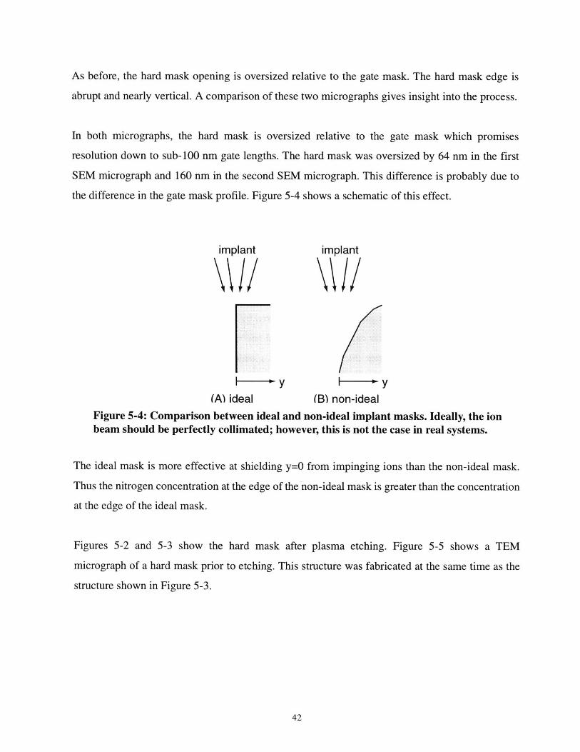
As before, the hard mask opening is oversized relative to the gate mask. The hard mask edge is
abrupt and nearly vertical. A comparison of these two micrographs gives insight into the process.
In both micrographs, the hard mask is oversized relative to the gate mask which promises
resolution down to sub-100 nm gate lengths. The hard mask was oversized by 64 nm in the first
SEM micrograph and 160 nm in the second SEM micrograph. This difference is probably due to
the difference in the gate mask profile. Figure 5-4 shows a schematic of this effect.
implant implant
1- -y I- -y(A) ideal (B) non-ideal
Figure 5-4: Comparison between ideal and non-ideal implant masks. Ideally, the ionbeam should be perfectly collimated; however, this is not the case in real systems.
The ideal mask is more effective at shielding y=0 from impinging ions than the non-ideal mask.
Thus the nitrogen concentration at the edge of the non-ideal mask is greater than the concentration
at the edge of the ideal mask.
Figures 5-2 and 5-3 show the hard mask after plasma etching. Figure 5-5 shows a TEM
micrograph of a hard mask prior to etching. This structure was fabricated at the same time as the
structure shown in Figure 5-3.
42

50nm
==50 nm 30 nm
50 nm
Figure 5-5: TEM micrograph of hard mask formed using CMBL.
As in Figure 5-3, the hard mask is oversized by 80 nm on each side. The hard mask also appears
to have been etched laterally by the TMAH. The hard mask edge has several interesting features.
A thin layer near the thermal oxide interface extends beyond the edge of the hard mask. The hard
mask also has a small lateral protrusion from the other corner of the hard mask edge. The lateral
etch rate appears to be slower at the silicon-oxide interface and at a depth corresponding to the
nitrogen implant peak. This variation in lateral etch rate may be due to the vertical nitrogen
profile. The nitrogen concentration is expected to be high at the interface due to nitrogen pile-up
[31]. The nitrogen concentration is also expected to be high near the implant peak (400-500 A
below the oxide-silicon interface). In addition to providing information on the hard mask edge,
the micrograph also shows an interesting gate profile. The original polysilicon gate had a
designed thickness of 1050 A. After the nitrogen implant, the nitride etch mask was stripped, and
the polysilicon step height was measured with a profilometer. The wide (2-3 gm) polysilicon lines
had a measured thickness of 1050 A while the sub-im polysilicon lines appeared to have a
thickness less than 1050 A. The polysilicon line in the micrograph does not appear to be 1050 A
thick. The center also appears to be thicker than the edges. For the most part, these micrographs
43
demonstrate that the hard mask is suitable for the intended use. These three micrographs
demonstrate that
- the hard mask is oversized relative to the original gate mask,
- the thickness of the hard mask is more than sufficient for use as an etch mask, and
. the hard mask edge is relatively abrupt.
While these results demonstrate the potential for high resolution, many issues still need to be
addressed. The next chapter summarizes the results of this work and discusses future directions.
44
Chapter 6
Summary
6.1 Conclusions
The double-gate MOSFET is necessary for scaling devices into the sub-50nm regime. The
fabrication of double-gate MOSFETs in which the top and buried gates are self-aligned remains a
serious challenge. The fabrication process should be manufacturable and should support buried
interconnect and other forms of 3-D integration.
This work demonstrates a self-alignment scheme that is used in conjunction with the flip, bond,
and etchback approach to forming buried gates. A gate on SOI material is used as a mask for a
chemical modification process that produces chemically modified regions that are self-aligned to
the masking gate. After the flip and bond step, the chemical difference is exploited to form a
second gate which is self-aligned to the first. The chemical modification process consists of a high
dose nitrogen implant that forms nitrogen-rich silicon just beneath the silicon-buried oxide
interface. TMAH is used to expose the nitrogen-rich silicon which later serves as a hard mask for
etching a trench that is self-aligned to the buried gate. This work demonstrates that the technique
is scalable to sub-100 nm geometries; however, many serious process integration issues still exist.
Future work will concentrate on resolving these issues.
45
6.2 Future Work
The CMBL process is primarily limited by process integration issues. In order for CMBL to be a
viable process, the CMBL process cannot damage the device. Ideally, the device should not be
exposed to an implant dose greater than 1x10 16 cm-2. Meanwhile, the selectivity must be
increased to relax the wafer thinning uniformity requirement. Future work will also examine
processes that produce a "positive" hard mask rather a negative mask. The etch profile achieved
using these masks will also be carefully examined.
46

Appendix AFlip, Bond, and Etchback Process
The fabrication sequence described in this appendix was designed to be used with densely packed
features with 1000-2000 A step heights.
- Deposit 1.5 gm LTOTube A7Recipe 462, FF=150 minutes
- Densify LTOTube B4Temperature = bonding anneal temperature + 50 0C
- Remove 0.8-1.0 gm LTOCMPTable Speed (rpm)/ Quill Speed (rpm) = 25/15Down Force (psi)/ Back Pressure (psi)= 4.0/2.5Slurry Flow Rate = 150 mL/minPad type = Rodel perforated IC 1000 w/ SUBA IV subpadSlurry Type = Cabot Semisperse 25Typical Rate = 22 A/s
- Grow 5000 A thermal oxide on handle waferTube A lRecipe 122, FF=91 minutes
- Bond device wafer to handle waferBonding jig at room temperature
- Anneal wafer pairTube B4
- Thin device wafer to 10 pmLincoln Laboratory (Andrew Loomis)
- Etch remaining silicon using TMAHKOH Hood75 0C using reflux condenser glassware
47

48

References
[1] P. Ko, Advanced MOS Device Physics (VLSI Electronics Microstructure Science Volume18), p.1, 1989.
[2] H. Hu, Experimental Study of Electron Velocity Overshoot in Silicon Inversion Layers,Ph.D. thesis, MIT, 1994.
[3] Y Taur et al., International Electron Devices Meeting, p.789, 1998.[4] D. Frank et al., International Symposium on Low Power Electronics and Design, p.3 17,
1997.[5] L. Su et al., IEEE Electron Device Letters, p.183, 1994.[6] C. Fiegna et al., Symposium on VLSI Technology, p.3 3 , 1993.[7] D. Frank et al., International Electron Devices Meeting, p.5 5 3 , 1992.[8] L. Yau, Solid-State Electronics, p.1059, 1974.[9] Z.-H. Liu et al., IEEE Transactions on Electron Devices, p.86, 1993.[10] D. Frank et al., IEEE Electron Device Letters, p.385, 1998.[11] T. Lochtefeld, private communication, 1999.[12] G. Shahidi et al., IEEE Electron Device Letters, p.94, 1988.[13] I. Yang et al., IEEE Transactions on Electron Devices, p.8 2 2 , 1997.[14] J.-P. Colinge et al., International Electron Devices Meeting, p.595, 1990.[15] H. Takato et al., IEEE International Electron Devices Meeting, p.2 2 2 , 1988.[16] D. Hisamoto et al., International Electron Devices Meeting, p.833, 1989.[17] H.-S. Wong et al., International Electron Devices Meeting, p.7 4 7 , 1994.[18] H. Smith, Submicron- and Nanometer-Structures Technology (2 nd Ed.), p. 19 -5 , 1994.[19] H.-S. Wong et al., International Electron Devices Meeting, p.4 27 , 1997.[20] B. Roberds et al., IEEE International SOI Conference, p. 10 9 , 1998.[21] J.-H. Lee et al., submitted to International Electron Devices Meeting, 1999.[22] S. Tiwari et al., DARPA Advanced Microelectronics Program Review, 1998.[23] T. Tanaka et al., International Electron Devices Meeting, p.683, 1991.[24] U. Schnakenberg et al., International Conference on Solid-State Sensors and Actuators,
p. 8 15 , 1991.[25] A. Chatterjee et al., International Electron Devices Meeting, p.821, 1997.[26] S. Wolf and R. Tauber, Silicon Processingfor the VLSI Era-Volume 1, p.251, 1986.[27] H. Stein, Oxygen, Carbon, Hydrogen, and Nitrogen in Silicon (MRS Volume 59), p.523,
1986.[28] A. Romano-Rodriguez et al., Nuclear Instruments and Methods in Physics Research B,
p.7 0 2 , 1993.[29] S. Wolf and R. Tauber, Silicon Processing for the VLSI Era-Volume 1, p.549, 1986.[30] D. Ouma, Modeling of Chemical Mechanical Polishing for Dielectric Planarization, Ph.D.
thesis, MIT, 1998.[31] M. Takayanagi-Takagi et al., International Electron Devices Meeting, p. 2 3 5 , 1997.[32] H. Soleimani et al., Journal of the Electrochemical Society, p.L132, 1995.[33] S. Furukawa et al., Japanese Journal of Applied Physics, p.134, 1972.
49

50