fast track pattern recognition in high energy physics
TRANSCRIPT
Fast Track Pattern Recognition in High Energy Physics Experiments with theAutomata Processor
Michael H. L. S. Wanga,∗, Gustavo Canceloa, Christopher Greena, Deyuan Guob, Ke Wangb, Ted Zmudaa
aFermi National Accelerator Laboratory, Batavia, IL 60510, USAbUniversity of Virginia, Charlottesville, VA 22904, USA
AbstractWe explore the Micron Automata Processor (AP) as a suitable commodity technology that can address the growingcomputational needs of track pattern recognition in High Energy Physics experiments. A toy detector model is de-veloped for which a track trigger based on the Micron AP is used to demonstrate a proof-of-principle. Althoughprimarily meant for high speed text-based searches, we demonstrate that the Micron AP is ideally suited to trackfinding applications.
Keywords: Pattern Recognition, Tracking, Trigger, Finite Automata
1. Introduction
Track pattern recognition occupies a central role in the reconstruction and analysis chains of practically all HighEnergy Physics (HEP) experiments because a particle’s trajectory carries crucial information on its properties andprovides a powerful signature to isolate it from unwanted background. With the advent of electronic detectors andreadout systems nearly 50 years ago [1], the manual scanning of tracks was transformed into a computational task.This task has grown more challenging with every new generation of experiment due to the trend towards more com-plex event topologies and higher particle densities. To cope with this trend, offline reconstruction applications haveso far relied on the rough doubling of transistors in many-core architectures every two years (Moore’s Law), whileonline applications with real-time requirements have traditionally relied on custom hardware solutions. Unfortunately,Moore’s Law becomes less dependable as we enter a period of diminishing performance returns where power dissipa-tion issues from leakage currents dominate as we approach the atomic scale [2]. On the other hand, custom hardwaresolutions are often accompanied by significant technical risks and require huge investments in manpower and capital.
In this paper, we take a different approach by exploring emerging commercial technologies designed to dealwith the deluge of digital information in today’s data centered economies. One such technology is the Micron Au-tomata Processor (AP) [3] which is specifically targeted at pattern matching applications like those in the Internetsearch industry and bioinformatics [4, 5, 6]. It is a direct hardware implementation of Non-deterministic Finite Au-tomata (NFA) and can simultaneously apply thousands of rules to find patterns in data streams at a constant rate of 1Gbps/chip. This capability, combined with a scalable architecture in a convenient off-the-shelf package, makes it anideal candidate for the growing needs of HEP track pattern finding. As a proof-of-concept to demonstrate its feasibil-ity for this application, we develop a simple toy detector model typical of those found at modern hadron colliders anduse the Micron AP to implement an electron track trigger.
2. The Automata Processor
2.1. Hardware ArchitectureBecause the Micron AP is based on a new and radical, non-von Neumann architecture, this section will provide a
description of the hardware, focusing on aspects relevant to our evaluation.
∗Corresponding authorEmail address: [email protected] (Michael H. L. S. Wang)
Preprint submitted to Nuclear Instruments and Methods in Physics Research A February 26, 2016
Mb
STE(0)
(255)
Mb(254)
Mb(253)
Logic
Mb(0)
Mb(1)
Mb(2)
Lo
gic
Me
mo
ry C
olu
mn
Bits (
1 x
25
6 )
ST
E (
1)
Lo
gic
Me
mo
ry C
olu
mn
Bits (
1 x
25
6 )
ST
E (
2)
Lo
gic
Me
mo
ry C
olu
mn
Bits (
1 x
25
6 )
ST
E (
3)
Lo
gic
Me
mo
ry C
olu
mn
Bits (
1 x
25
6 )
ST
E (
N-3
)
Lo
gic
Me
mo
ry C
olu
mn
Bits (
1 x
25
6 )
ST
E (
N-2
)
Lo
gic
Me
mo
ry C
olu
mn
Bits (
1 x
25
6 )
ST
E (
N-1
)
Lo
gic
Me
mo
ry C
olu
mn
Bits (
1 x
25
6 )
ST
E (
N)
Automata Routing Matrix Structure
ST
E(0
)In
puts
ST
E(0
)O
utp
ut
State Transition Clock(common)
Row Enable (0)(common)
Row Enable (1)(common)
Row Enable (2)(common)
Row Enable (253)(common)
Row Enable (254)(common)
Row Enable (255)(common)
8 bits
InputSymbol
8 to 2
56
“row
addre
ss”
deco
der
256 r
ow
by 4
9,1
52 c
olu
mn
Mem
ory
Arr
ay
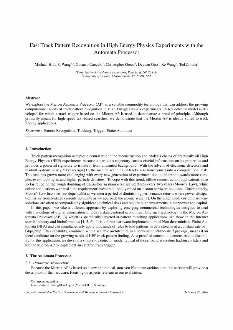
Figure 1: The 2D memory array architecture of the Micron Au-tomata Processor adapted from conventional SDRAM technology.
Outputregion
Outputevent
memory
Outputregion
Outputevent
memory
Outputregion
Outputevent
memory
Half CoreOutputregion
Outputevent
memory
Outputregion
Outputevent
memory
Outputregion
Outputevent
memory
Half Core
64 KB 64 KB
Automata Processor Core
Outputeventbuffer
Reporting results(DDR3)
1024 bits
64bits
10
24
ve
cto
rs
Flow inputbyte offset
Reportingevent vector
Figure 2: Reporting event vector readout architecture.
2.1.1. A Memory-based DesignThe Micron AP is derived from conventional SDRAM technology and its hardware architecture (see Figure 1) is
conveniently understood in terms of a two-dimensional memory array. Each input byte on an 8-bit wide bus servesas a row address which is presented to an 8-to-28 decoder that selects one out of 256 possible rows. A column of256 cells in this array, together with additional logic for state information, comprises the basic building block of theAP known as a State Transition Element (STE). Any cell or combination of cells in an STE can be programmed torecognize any subset of 28 possible values or symbols. When the address decoder selects a cell in an enabled columnor STE, which is programmed to recognize its associated symbol, the stored value of “1” is output to indicate symbolrecognition. This causes the STE output to change state and can be used to enable other downstream STEs. MultipleSTEs, each programmed to recognize specific symbols, can be chained together to recognize patterns or strings ofsymbols. Such patterns need not be limited to ASCII strings and could just as well represent hit addresses associatedwith a particle trajectory in a tracking detector. The interconnections between the STEs is provided by the routingmatrix structure, represented by the block at the bottom of Figure 1, which plays the role of the column address anddecode operations.
2.1.2. Reporting Pattern MatchesThe Micron AP was specifically designed to perform high-speed pattern recognition. To be useful in this applica-
tion, there must be an efficient way to tell whether pattern matches were found and provide details on these matches.To this end, any AP building block such as an STE, counter, or boolean can be configured to generate a signal knownas a report event whenever it recognizes an input symbol. This way, the last element in a string of STEs programmedto recognize a sequence of symbols in an expression, can generate such a signal to indicate a matching pattern in theinput data stream.
The portion of the AP architecture relevant to match reporting is shown in Figure 2. The AP is divided into 2 halfcores, each of which has 3 output regions. Each region has a local storage area known as the output event memory withroom for 1024 output event vectors (or report vectors) that are up to 1088 bits wide. Each vector has a 64-bit preambleused to indicate the offset from the start of the input data stream. The remaining 1024 bits are used to identify theelement in the region that generated the report event. In this respect, the AP is unique because it provides both spatialand temporal information on the matches.
An output event vector is generated on every symbol cycle for which there was a report event in that region. Sinceeach vector is associated with a symbol cycle, events occurring on the same cycle require a single vector while eventson different cycles require separate vectors. When symbol processing completes, the vectors are transferred from eachregion’s output event memory to the output event buffer, where they can be read by external hardware.
2

AP AP AP AP AP AP
RØ view RZ view
Detector hits
Hits in RØ view Hits in RZ view
Report vectorsin RØ view
Report vectorsin RZ view
Trigger accept
Coincidencelogic and
triggergeneration
Pre-processor
Figure 3: Block diagram of Automata-Processor-based track trig-ger hardware.
1 05 24 39 68 7101112131415
Layer(2 bits)
Face(6 bits)
ROC (1 bit)
Row(7 bits)
{
R- :
3 02 17 46 511 810 91213
Layer(2 bits)
Module(3 bits)
ROC(3 bits)
Column(6 bits)
R-Z:
Figure 4: Data encoding scheme for pixel addresses in the R − φand R − z views.
2.1.3. Additional LatenciesIdeally, the total processing time would depend only on the number of input symbols. In reality, there are overheads
tied to the internal memory transfers described above which introduce additional latencies. There is an overheadassociated with transferring each vector from a region’s event memory to the output buffer. There is also a start-upoverhead associated with transferring the first vector to the output buffer. Just to determine that a region is emptyalso incurs an overhead. The overhead due to transferring each vector depends on its size and can be reduced byconfiguring the AP to use smaller vectors.
2.2. Programming the Automata ProcessorThe Micron AP is programmed using tools provided in the AP Software Development Kit (SDK). The process
begins by creating a human-readable representation of the automata which can be done through a graphical tool knownas the AP Workbench. This representation is transformed into machine-readable form in the compilation step whichinvolves optimization and placing and routing the automata elements onto the AP fabric. This produces a binaryrelocatable image that is loaded and executed on the AP hardware.
3. Proof of Principle: An Electron Track Trigger
To investigate the feasibility of the Micron AP in HEP track finding, we consider an electron trigger applica-tion where isolated high pT electrons are identified in a hadron collider detector by matching energy clusters in anelectromagnetic (EM) calorimeter with charged particle tracks in a pixel-based tracking detector. A simplified blockdiagram depicting the track trigger hardware architecture is shown in Figure 3. Incoming pixel detector hit data aredecomposed into the R − φ (bend plane) and R − Z (non-bend plane) views and fed into two separate banks of APchips that perform the track finding in each view. The reporting event vectors in each view are read out of each bankand fed into external logic that determines if there is at least one pair of reporting events (one from each view) thatare correlated in time. If this condition is satisfied, a trigger accept signal is generated.
3.1. Toy DetectorFor our proof-of-principle studies, we developed a toy detector model consisting of 4 concentric cylinders approx-
imating the barrel portion of the CMS Phase-1 pixel detector [7]. The geometry and specifications of this model aredescribed in Table 1. All pixels in the entire detector have dimensions measuring 165 × 98 µm with the longer axisoriented along the beam axis (z). The pixels in each layer form a uniform grid laid out over the entire cylindricalsurface. This means that the face of each pixel is really a cylindrical tube segment instead of a flat rectangular area.
3

Layer Radius (cm) Faces Modules ROCs Pixels in φ Pixels in z Total pixels1 2.99 12 96 1536 1920 3328 6 389 7602 6.99 28 224 3584 4480 3328 14 909 4403 10.98 44 352 5632 7040 3328 23 429 1204 15.97 64 512 8192 10 240 3328 34 078 720
Length of the toy pixel detector 54.88 cm
Table 1: Toy pixel detector specifications. Each face is a ladder consisting of 8 sensor modules. Each sensor module is made up of a pixel sensorbonded to 2 rows of 8 Read-Out-Chips (ROCs) each. Each ROC has 80 rows × 52 columns of pixels. Each pixel sensor measures 165 × 98µm.
Pixel addresses or coordinates are encoded using the 16-bit and 14-bit data formats shown in Figure 4 for the R − φand R − z views, respectively.
For the purposes of defining the regions of interest (ROI) used in detector data readout and defining the patternbanks used by the automata processor (both discussed in more detail below), we divide the pixel detector into logicalsections in the R − φ and R − z views (see Figure 5). In the R − φ view, the detector is divided into 72 overlappingazimuthal sectors, each measuring 25◦ in φ. In the R − z view, layer 1 is divided into 32 equal sections in z and eachof layers 2, 3, & 4 into 16 equal sections in z. Taken together, the logical divisions in both views form cylindrical tubesegments in each layer which we will refer to as tiles. An example of these tiles being used to define the ROIs fortrack searching is shown in Figure 6.
Surrounding the pixel detector is a larger concentric cylinder representing the barrel portion of the EM calorimeterwith a radius of 129 cm and eta coverage of ±1.479. We assume a single crystal barrel granularity of 180-fold in φ(half that of the CMS detector) and 2 × 85 fold in η.
L1
L2
L3
L4
0 1 2 310 1 2
0 1 2 15
a
b
R-Ø view R-z view
Figure 5: The toy detector is divided into 72 overlapping sectors in the R − φ view. Examples of two such neighboring sectors, the 12th in red andthe 13th in green, each measuring 25◦ are shown above. In the R − z view, each layer is divided into equal sections in z — 32 for layer 1 and 16for all other layers. Shown in blue, red, and green are examples of combinations of 4 sections (1 from each layer) forming roads of straight tracksoriginating from the luminous region and within the fiducial volume of the detector.
3.2. Simulated Events
Simulated events are generated with proton-proton collisions at 14 TeV center-of-mass energies using Pythia6.4 [8] with CMS Tune Z2* [9] parameters. These events consist of Z → ee signal events overlaid with pileup eventswhich are pure Monte-Carlo minimum bias events. The number of pileups overlaid on each signal event is randomlychosen from a Poisson distribution. The positions of the primary interaction vertices along the z-axis are randomly
4
(a) (b)
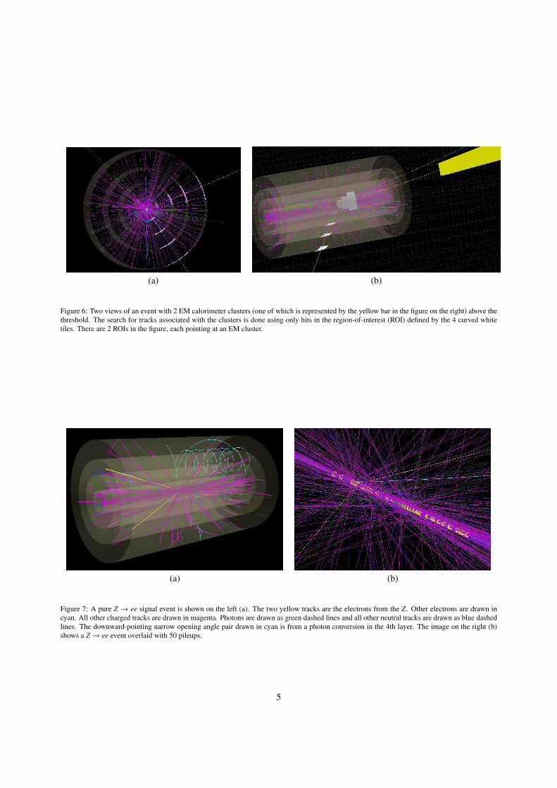
Figure 6: Two views of an event with 2 EM calorimeter clusters (one of which is represented by the yellow bar in the figure on the right) above thethreshold. The search for tracks associated with the clusters is done using only hits in the region-of-interest (ROI) defined by the 4 curved whitetiles. There are 2 ROIs in the figure, each pointing at an EM cluster.
(a) (b)
Figure 7: A pure Z → ee signal event is shown on the left (a). The two yellow tracks are the electrons from the Z. Other electrons are drawn incyan. All other charged tracks are drawn in magenta. Photons are drawn as green dashed lines and all other neutral tracks are drawn as blue dashedlines. The downward-pointing narrow opening angle pair drawn in cyan is from a photon conversion in the 4th layer. The image on the right (b)shows a Z → ee event overlaid with 50 pileups.
5

selected from a Gaussian distribution centered at z = 0 cm with σz = 5 cm. For simplicity, the transverse positions ofthe primary vertices are always centered at x = y = 0 cm. Figure 7-a shows a 3D view of a simulated pure Z → eesignal event. Figure 7-b shows a Z → ee event overlaid with 50 pileup events.
Starting from the production vertices, all particles are tracked through the toy detector model with a uniform4T axial magnetic field. All unstable particles are allowed to decay randomly into a channel selected according totheir branching fractions and with exponential decay length distributions based on their proper lifetime. Photons areconverted into electron-positron pairs with the appropriate small opening angle distribution at a frequency determinedby the pair production cross section (for both nuclear and electronic fields) in the material of the detector concentratedin the 4 pixel detector layers. We use a fictitious sensor module material with an effective Z and density (ρ) determinedfrom the various components of an actual CMS pixel sensor module. To keep things simple in this proof-of-conceptinvestigation, no other physics processes such as multiple scattering and energy loss mechanisms are simulated. Allcharged particles traversing a pixel detector layer generate a single pixel hit for that layer with 100% efficiency. Theaddress of the hit is determined from the coordinates of the intersection of the trajectory with the cylinder. Onlyelectromagnetic particles (electrons and photons) above a threshold of pT = 5 GeV are propagated beyond layer 4 ofthe pixel detector to the EM calorimeter barrel. Upon reaching the calorimeter, the total energy of such an EM particleis deposited into the calorimeter crystal it intersects to generate an EM cluster.
Four different 1000-event samples were generated having Poisson means for the number of overlaid pileups ofN = 50, 80, 110, & 140. All four samples used the same set of Z → ee signal events.
4. Implementing the Track Finder on the Automata Processor
4.1. Basic Automata Network and Principle of Operation
Figure 8: An automata network programmed to generate a report on matching a specific sequence of exactly 4 pixel hit addresses.
The application of the automata processor as a fast pattern search engine is based on the idea of maintaininga database or dictionary of all possible patterns against which symbols in an input data stream are simultaneouslycompared for matches. The patterns in this dictionary can be all the possible words in a language or, in our case, allphysically possible charged particle trajectories in a tracking detector. In our present case, each possible trajectory isdefined by the addresses of 4 pixel hits representing the intersection of the trajectory with each layer of the detector.On the automata processor, each pattern of 4 pixel addresses representing a trajectory in the dictionary is associatedwith the automata network having the topology shown in Figure 8. As shown, this network consists of 9 columns of2 STEs each. The pixel addresses are stored in the STE pairs labeled Lx lo and Lx hi with x=1,2,3,4 denoting thedetector layer. Since each STE only has 8 bits of symbol recognition capability, the least and most significant bytesof each address are stored separately in Lx lo and Lx hi, respectively. The STE pair to the left of each (Lx lo, Lx hi)pair acts as a latch that re-enables the Lx lo STE on its right only on odd clock cycles. This ensures that pair of bytesdenoting a pixel address are contiguous and can occur anywhere in the input data stream. The very first pair of STEson the left of the figure imposes additional constraints for each pattern. Assuming that the very first symbol in an input
6

data stream represents the energy of the EM cluster for which we are trying to find a track match, the STE labeledET requires this energy to be within the possible range for the stored track pattern. Below this, the STE labeled Caloholds the address of the EM calorimeter crystal that trajectory intersects.
To illustrate the operation of this automata network, consider an input data stream from the detector, consisting ofpixel hit addresses read out sequentially by layer, starting from the innermost. Assume that the very first symbol inthe input data stream is an 8-bit number representing the EM calorimeter cluster energy and that the second symbolrepresents the address of the EM calorimeter crystal associated with the cluster. If the energy of the measured clusterfalls within the range of the ET STE, its output is enabled, thereby activating the Calo STE. If the crystal addressmatches that in the Calo STE, this STE enables its output and activates the L1 lo STE. After this point, if a symbolanywhere in the data stream matches that in L1 lo, the output of this STE is enabled, activating L1 hi. If the imme-diately following symbol matches that in L1 hi, then L2 lo is activated to wait for matching hits in the 2nd layer ofthe detector. On the other hand, if no match is found for L1 hi, we need to keep reactivating L1 lo every other clockcycle until we find a layer 1 match. This is the purpose of the OC 0x pair of STEs which reactivates L1 lo on everyodd clock cycle, re-initializing the search for the byte-pair representing the layer 1 hit. These steps are repeated forevery detector layer until either 4 matching pixel hits are found or the input data stream is exhausted.
4.2. Generating the Dictionary or Pattern Banks
Figure 9: Generating all possible track patterns with a single electron gun monte carlo event generator for a given region of the detector.
We generate our pattern banks separately for the R − φ bend view and for the R − z non-bend view. For the R − φview, the patterns are generated for each ±12.5 degree φ-sector described earlier in Section 3.1. For the R− z view, westart with the same subdivisions along z in each detector layer described in Section 3.1. We will refer to each divisionas a window. We take all possible combinations of 4 windows (one from each layer) forming roads containing straightlines originating from the luminous region and ending in the EM calorimeter barrel. Patterns are then generated foreach road.
To generate the pattern banks, we use a single electron gun monte carlo event generator to produce all the possibletracks above pT = 5 GeV. Figure 9 shows the process of generating these patterns for a given region of the detector.Electrons of both charges are generated and propagated through the toy detector model described in Section 3.1generating pixel hits as they traverse each layer. Just as with our simulated Z → ee events with pileups, we do notsimulate energy loss or multiple scattering when generating the pattern banks.
To keep the total number of patterns manageable, we use a resolution of 4 pixels for all detector layers in eachview. There is a total of 72 pattern banks in the R − φ view with each bank having ∼1163 unique track patterns. Dueto the rotational symmetry of the ideal toy detector about the z axis, each bank has an identical set of patterns moduloa rotation in φ. One could, in principle, use a single bank to represent the entire detector in the R − φ view after theappropriate rotation is applied to the hits of a given sector. We chose not to do this since perfect rotational symmetrymay not be present in a real detector. For the R − z view, we consolidate all roads with a common layer 1 and layer4 window into a single bank resulting in a total of 244 pattern banks. The average number of track patterns in eachbank is ∼4662. For the ideal toy detector, there is a mirror symmetry about the x − y plane in this view. The set oftrack patterns in each half are identical modulo a translation in z. Again, we chose not to exploit this symmetry sinceit may not be present in a real detector.
7

These pattern banks are programmed into the automata processor using the C-API provided in the AP SDK. Foreach entry in a generated pattern bank, an instance of a macro representing the basic automata network shown inFigure 8 is created by substituting its parameters with the values associated with the current pattern. The result-ing automata network containing all instances is then compiled into an object file that is loaded into the automataprocessor.
We can compile 2,496 instances of the macro shown in Figure 8 onto the current version of the AP chip. Withouttaking advantage of rotational or translational symmetries, this would require about 34 chips for the R − φ view and456 chips for the R − Z view. With the current AP boards that have 4 ranks of 8 chips each, this translates to about 1board for the R − φ view and 14 boards for the R − Z view.
4.3. Available Features and Capabilities and Possible Improvement
Layer 1 hit
Layer 2 hit
Layer 2 hit
Layer 3 hit
Layer 3 hit
Layer 4 hit
R
R
L1_lo L1_hi
L2_lo L2_hi L3_lo L3_hi
L2_lo L2_hi
L4_lo L4_hi
L3_lo L3_hi
Latch
Latch
Latch
Latch
Latch
* *
* *
* * * *
* *
Figure 10: An automata network programmed to generate a report on matching a sequence of 4 pixel hit addresses allowing up to one missing hit.
The simple automata network shown in Figure 8, requiring hits in all 4 layers of the detector, suffices for thepresent purpose of demonstrating a proof-of-principle. However, it is possible to design an automata-based algorithmthat can deal with missing hits due to inefficiencies in a real detector. An automata network representing a trackpattern allowing up to one missing hit in any layer is shown in Figure 10.
Another interesting feature of the AP is the STE’s ability to recognize a range of values instead of a specific one.This makes it possible to employ variable resolution patterns that offer a way to reduce the total number of patterns ina bank [10].
Lastly, the number of STE’s (18) in Figure 8 needed to represent a specific track pattern is largely due to thelimited alphabet size of 8 bits. If our alphabet size were 16 bits, we could reduce the number of STEs by a factor of3 to just 4 STEs representing the 4 hits plus two additional STEs for the calorimeter energy and position. This wouldreduce the total number of automata chips needed for our pattern banks.
5. Testing the AP-based Track Finder with the Simulated Samples
To satisfy the requirements of the electron track trigger application described in Section 3, the AP must, first ofall, be able to reconstruct tracks for electron/photon discrimination. Secondly, it must be able to accomplish this taskwithin the available latency of the trigger [11]. This section will focus on its track finding ability. The next sectionwill focus on its processing times.
5.1. Testing Procedure
For each of the simulated events described in Section 3.2, we check to see if there are EM calorimeter clusters.For each cluster above the threshold, we then read out all the pixel hits within the ROI associated with the cluster (seeFigure 6). The extents of the ROI in the R− φ view are defined by the boundaries of the φ sector (1 of 72 described inSection 3.1) whose bisector is closest in azimuthal distance to the cluster.
8

Number of EM Clusters Track Match Efficiency Rejection PurityPileups Total Electrons Photons Electrons Photons (%) Factor (%)
50 1242 837 405 837 9 100 45 9980 1395 839 556 839 17 100 33 98
110 1515 844 671 844 26 100 26 97140 1648 844 804 844 56 100 14 94
Table 2: This table summarizes the ability of the Automata Processor algorithm to identify electrons and reject photons for each of the 4 simulatedsamples used in our study. The total number of EM clusters and their breakdown into electrons and photons are shown in columns 2-4. Columns 5and 6 show the number of electron clusters and photon clusters, respectively, for which a matching track was found. The last three columns showthe electron identification efficiency, photon rejection factor, and purity as defined in the text.
In this proof-of-principle study, we also assume single (double) crystal calorimeter resolution in the R − Z (R − φ)view and precise knowledge of the interaction vertex associated with the Z → ee signal. In the R − z view, we firstconstruct a straight line defined by the calorimeter cluster coordinates (center of the single crystal) and the primaryinteraction vertex. We then find the layer 1 and layer 4 windows this line intersects. Together with this pair, all layer 2and layer 3 windows that form roads (see Section 4.2) with the pair are used to define the ROI extents in the R−z view.If such a ROI exists within the acceptance of the pixel detector, we will refer to the EM cluster as reconstructable.All the pixel hits within the ROI defined this way are read out sequentially by layer starting with the innermost. Thesequence of the hits within each layer in the data stream does not matter to the automata track finding algorithm. Thisdata stream of pixel hits arranged by layer is appended to two 8-bit quantities, the first for the EM cluster energy andthe second for the EM calorimeter crystal coordinate. The 8-bit stream is fed into the automata hardware containingthe pattern banks corresponding to the ROI. This is done separately for the R − φ and R − z views. In the hardware,all the instances of the macro represented by Figure 8 associated with the bank are simultaneously presented with theinput data stream to generate reports in case of matches. A trigger accept is generated if matches are reported in bothviews on the same clock cycle.
5.2. Results for Electron Identification and Photon Rejection
For our tests, we require all reconstructable clusters to have pT > 5 GeV. Clusters produced by electrons arerequired to originate from the beam axis. The total number of EM clusters satisfying these requirements for eachof the 1000-event simulated samples overlaid with a different number of pileups are shown in the second column ofTable 2. A breakdown of these numbers into those originating from electrons and those from photons is shown in thethird and fourth columns. The fifth column of the table shows the number of electron clusters for which a matchingtrack was found. The same number for photons is shown in the sixth column.
For this study, we define the electron identification efficiency as εe = NeEMtrk/N
eEM and the photon rejection factor
as Rγ = NγEM/N
γEMtrk. Ne
EM and NγEM are the number of reconstructable EM clusters originating from electrons and
photons (columns 3 and 4 of Table 2), respectively, which satisfy the requirements described at the beginning of thissection. Ne
EMtrk and NγEMtrk are the corresponding numbers of EM clusters for which there is a matching track in the
pixel detector (columns 5 and 6 of Table 2). The results for εe and Rγ are shown in the last two columns of Table 2. Forall samples, we see that the AP algorithm correctly finds a matching track for every electron EM cluster satisfying ourrequirements. The fraction of photon EM clusters satisfying our requirements that are misidentified increases from2% to 7% as the number of the pileups in the sample, and hence detector occupancy, increases. The last column inTable 2 shows the purity Pe = Ne
EMtrk/(NeEMtrk + Nγ
EMtrk), which we define as the fraction of all EM clusters satisfyingour track trigger requirements that originated from an electron.
6. Processing Time
The amount of time it takes the AP to find matching tracks in each view (which we will refer to as symbolprocessing time) depends only on the number of hits in the ROI. Because we are using 16-bit hits while the AP usesnative 8-bit symbols, the total number of input symbols is twice the number of hits. Since one symbol is processed
9

Number of pileups
40 60 80 100 120 140
Sym
bo
l cycle
s
150
200
250
300
350
400
450
Number of pileups
40 60 80 100 120 140
Sym
bo
l cycle
s
150
200
250
300
350
400
450
viewφR Rz view
assuming 512bit report vectors assuming 512bit report vectors
Figure 11: Shown above are the symbol cycles to process the hits in each view and transfer the report events to the output event buffers on an APchip. This is plotted as a function of the simulated samples overlaid with N = 50, 80, 110, and 140 pileups.
per AP clock cycle, the symbol processing time is simply equal to the number of input symbols. This time doesnot represent the total processing time since the match results in each view need to be read out of the AP chips andundergo further processing to find coincident matches in each view before making a trigger decision. This additionaltime includes (a) the internal data-transfer time within the AP to move the match results from the local event memoriesin the six output regions to the output event buffers (see Section 2.1.2), and (b) the external processing time in externallogic to find coincident reports in both views. The internal transfer time depends on the size of the report vectors andtheir number in each of the six regions. In addition, there are overheads associated with determining a region to beempty and a startup overhead for reading the first vector. What we refer to as the external processing time includesthe data-transfer time from the AP’s event output buffer to the external logic across the DDR3 interface. The symbolprocessing and internal data transfer will be collectively referred to as core processing since they both occur on theAP chip. The first subsection below will focus on the core processing followed by a second subsection devoted to theexternal processing.
6.1. Core Processing Time
To calculate the number of symbol processing cycles, we simply multiply the number of hits by two. For bothviews, we add an additional symbol cycle to process the 8-bit symbol representing the coordinates of the calorimetercrystal. For the R − φ view, we add one more symbol cycle to account for the 8-bit symbol representing the energy ofthe cluster.
As we explained earlier, two report events occurring on the same symbol cycle are saved in either the same ordifferent event vectors depending on the output region they occurred in. As we also pointed out, it takes a finitenumber of symbol cycles to transfer each vector. Because of this, when calculating the internal data-transfer time,we randomly assign a report event to one of the six output regions. This assumes there is no correlation between theautomata instances representing all the patterns in our bank and that they are uniformly distributed throughout the 6regions. We use an event vector divisor of 2 to reduce the vector width to 512 bits and assign the appropriate numberof symbol cycles to transfer a vector of this size. We also take into account the overheads associated with “reading”an empty region and transferring the first vector. The symbol processing times plus internal data-transfer times foreach view are shown as a function of the simulated sample in Figure 11. For a symbol cycle of 7.5 ns, these translateto 1.29, 1.55, 1.85, and 2.15 µs, respectively, for the 50, 80, 110, and 140 pileup samples in the R − φ view. Thecorresponding times for the R − Z view are, respectively, 1.49, 1.94, 2.53, and 3.25 µs.
10

Number of pileups40 60 80 100 120 140
CP
U c
ycle
s
20
40
60
80
100
120
140
160
180
200
220
310×
CPU processing time
nomatch
all
matched
Single threaded
Number of pileups40 60 80 100 120 140
CP
U c
ycle
s
10
20
30
40
50
60
70
803
10×
CPU processing time
nomatch
all
matched
Multithreaded
using OpenMP
Number of pileups40 60 80 100 120 140
CP
U c
ycle
s
20
40
60
80
100
120
140
160
180
200
220
310×
GPU processing time
nomatch
all
matched
(a) (b) (c)
Figure 12: The plots above show the number of cycles to process the pixel track trigger algorithm described in Ref. [12] as a function of thesimulated data samples for the (a & b) Intel Core i7 CPU and the (c) nVidia Tesla GPU described in the text. Results for the Intel CPU are shownseparately for the (a) single threaded and (b) multithreaded cases. Data-transfer times between host and GPU are not included in the results for(c). In all cases, the cycles are measured using the Intel CPU’s time stamp counter. Dashed-line plots with upright triangular markers are obtainedusing only EM clusters for which no track match is found. Dashed-line plots with inverted triangular markers are obtained using only EM clustersthat have at least one matching track. The solid-line plots and solid circular markers are obtained using all EM clusters.
6.2. External Processing Time
After all detector hit data associated with an EM cluster are processed by the AP banks for the R − φ and R − Zviews, the last step of our track finding algorithm requires checking for at least one pair of reporting events (one fromeach view) in which the R − Z event occurred one symbol cycle ahead of the R − φ event. This 1-cycle difference isdue to the fact that the automaton representing a track in the R− Z view has one less STE than that for the R− φ view.This requirement does not guarantee a common source for both events, but those that do originate from the same trackwill necessarily exhibit this correlation in time, and this constraint can only help reduce fake rates.
To estimate the processing time associated with finding at least one pair of correlated reporting events, we imple-mented the Content Addressable Memory (CAM) reference design described in Reference [13] on a 100 MHz XilinxVirtex-6 LX240T FPGA. Our studies are based on simulations done using the Xilinx ISE Design Suite. We assumethat the report vectors can be read out of the Micron AP’s 8-bit wide bus at 1066 MHz. In our simulations, the 576-bitdata (64-bit header + 512-bit reduced-size vector) associated with each vector is read out from the R − Z banks andthe 64-bit header containing the temporal information is extracted and written into FPGA memory. Once the headersfrom all R − Z view vectors associated with an EM cluster are stored in memory, we loop over the correspondingheaders from the R − φ view vectors and present them to the CAM to find the first match. As soon as this is found, atrigger accept signal is generated and the process is repeated for the next EM cluster.
For the 1000-event sample overlaid with 140 pileups, the average time to execute this match finding step on theFPGA is 0.37 µs, which is insignificant compared to the core processing time.
7. Comparison with other Processor Architectures
For comparison, we compile a single threaded C-version of the pixel-based tracking trigger algorithm describedin Ref. [12] using the Intel C compiler (v16.0.1). We then run it on a 3.3 GHz Intel Core i7 (5820K) processor usingthe same four simulated data samples. Using the Intel CPU’s time stamp counters, we measure the number of CPUcycles to execute the trigger for each EM cluster and plot the mean as a function of the sample in Figure 12a with asolid line and solid circular markers. For a 0.3 ns CPU clock cycle, these results translate to 3.38, 7.60, 16.7, and 32.1µs, respectively, for the 50, 80, 110, and 140 pileup samples.
The processing cycles are also shown separately for EM clusters with at least one matching track (dashed line withupright triangular markers) and EM clusters with no matching tracks (dashed line with inverted triangular markers).
11

Clusters with matching tracks require less processing time because the algorithm quits forming all possible combina-tions of 4 hits as soon as a matching track is found. The opposite is true for clusters with no matching tracks since thealgorithm ends up attempting all possible combinations.
These results clearly exhibit a quadratic rise in processing times which increases by at least an order of magnitudein going from 50 to 140 pileups. In contrast, the results in Figure 11 show that the AP processing times scale almostlinearly as the number of pileups in the samples is increased. The processing times increase only by less than a factorof 2× in going from 50 to 140 pileups.
Using OpenMP, we created a multithreaded version of the code described above and compiled it with the sameversion of the Intel C compiler. The results for this multithreaded implementation on the Intel CPU described above,with 6 physical cores (12 logical cores because of Hyper-Threading), are shown in Figure 12b for the four simulatedsamples. The meanings of the markers and line types used in the plot are identical to those in Figure 12a. The averageprocessing times are 5.23, 7.85, 11.7, and 17.5 µs, respectively, for the 50, 80, 110, and 140 pileup samples. The resultfor the 140 pileup sample is ∼ 2× faster than the single threaded CPU result and ∼ 5× slower than the AP result.
We also implemented the algorithm described in Ref. [12] on an nVidia Tesla K40c GPU (745 MHz) using nVidia’sCUDA programming environment. In this case, the loops over 4-layer hit combinations were unrolled using parallelthread blocks where each thread block dealt with one hit combination from Layers 1 and 4. Multiple threads in eachblock then dealt with Layer 2 and 3 hit combinations in parallel. The number of processing cycles as a function ofsample for the GPU are shown in Figure 12c. The processing cycles are measured using the host Intel CPU’s timestamp counters. The legend used in the graph is identical to that for the CPU with results shown for all clusters andseparately for the two classes of clusters described above. The average GPU processing times are 34.8, 38, 44.8, and53.7 µs, respectively, for the 50, 80, 110, and 140 pileup samples.
The GPU results do not show improvement over the CPU results, mainly because it is more complicated forthe GPU to break out of a loop upon the first successful track match, or for it to skip to the next iteration of a loopthrough continue statements. This makes the execution time dependent on the slowest thread. The parallel capabilitiesof the GPU are also not fully exploited by our test case where we have significantly reduced the combinatorics byconsidering only hits within the ROI. Furthermore, one must also take into account additional latencies associatedwith data transfers between the CPU and GPU, which contribute an additional > 91K CPU cycles (> 27 µs) to thetotal cycles (time). One place where the GPU does better, however, is on events in the tail of the execution timedistributions of the CPU. Such events have little influence on the spread of the GPU distributions because the GPUexcels at dealing with problems that have more massive parallelism.
The algorithm described in Ref. [12] used in the CPU/GPU comparisons above is functionally but not algorith-mically equivalent to our automata-based track finder. Using regular expressions to represent hit patterns, we alsoimplemented an algorithmically equivalent NFA-based solution on the same GPU used above. We measure ∼ 10seconds to execute the algorithm for each cluster which is about 6 orders of magnitude longer than on the AP.
8. Conclusion
We have successfully demonstrated a proof-of-concept for the suitability of the Micron Automata Processor inparticle track finding applications for experimental HEP. Up to now, most applications of this technology have beenlimited to text-based searches. This signifies the first use of this interesting technology to the recognition of visualpatterns. It opens up a whole new realm which may even include image processing applications in fields like astron-omy. Furthermore, our studies indicate that this technology may be suitable for demanding real-time applicationssuch as online triggers in HEP experiments. Compared with other commodity off-the-shelf solutions like CPUs andGPUs, the AP requires a factor of over two orders of magnitude fewer hardware cycles to perform our sample trackfinding application. While our multithreaded implementation of the algorithm in Ref. [12] is less than an order ofmagnitude slower than our AP-based track finder, one must keep in mind that the Intel CPU used in this study is the5th generation of a very mature technology. Pre-production evaluation versions of the AP are only becoming availablenow at the time of this writing. In our evaluation, we were also conservative in our choice of configurable parame-ters such as the size of the report vectors. Choosing a smaller size can further reduce the times associated with theinternal transfer and readout of these vectors. Future versions of the AP may also incorporate larger alphabet sizes.Doubling the current symbol recognition capability from 8-bits to 16-bits, for example, will cut the time to process
12

16-bit hit addresses in our track finding algorithm in half. The possibility of such improvements, coupled with theresults presented in this paper, suggest that this may be a promising technology worthy of more detailed considerationin real-world HEP pattern recognition applications.
9. Acknowledgements
We are grateful to David Christian, Aurore Savoy-Navarro, Chang-Seong Moon, Ted Liu, and Ken Treptow forvaluable discussions. We thank the supportive staffs at the University of Virginia’s Center for Automata Processingand Micron Technology for their technical assistance. Fermilab is operated by Fermi Research Alliance, LLC underContract No. De-AC02-07CH11359 with the United States Department of Energy.
References
[1] G. Charpak, R. Bouclier, T. Bressani, J. Favier, C. Zupancic, The use of multiwire proportional counters to select and localize chargedparticles, Nuclear Instruments and Methods 62 (3) (1968) 262–268. doi:10.1016/0029-554X(68)90371-6.
[2] N. S. Kim, T. Austin, D. Blaauw, T. Mudge, K. Flautner, J. S. Hu, M. J. Irwin, M. Kandemir, V. Narayanan, Leakage current: Moore’s lawmeets static power, Computer 36 (12) (2003) 68–75. doi:10.1109/MC.2003.1250885.
[3] P. Dlugosch, D. Brown, P. Glendenning, M. Leventhal, H. Noyes, An efficient and scalable semiconductor architecture for parallel automataprocessing, IEEE Transactions on Parallel and Distributed Systems 25 (12) (2014) 3088.
[4] K. Wang, Y. Qi, J. J. Fox, M. R. Stan, K. Skadron, Association rule mining with the micron automata processor, in: Proceedings of the 2015IEEE International Parallel and Distributed Processing Symposium, IPDPS ’15, 2015, pp. 689–699. doi:10.1109/IPDPS.2015.101.
[5] K. Zhou, J. J. Fox, K. Wang, Y. Qi, D. E. Brown, K. Skadron, Brill tagging on the micron automata processor, in: Proceedings of the 2015IEEE International Conference on Semantic Computing, ICSC ’15, 2015, pp. 236–239. doi:10.1109/ICOSC.2015.7050812.
[6] I. Roy, S. Aluru, Finding motifs in biological sequences using the micron automata processor, in: Proceedings of the 2014 IEEE 28thInternational Parallel and Distributed Processing Symposium, IPDPS ’14, IEEE Computer Society, Washington, DC, USA, 2014, pp. 415–424. doi:10.1109/IPDPS.2014.51.
[7] A. Dominguez, et al., CMS Technical Design Report for the Pixel Detector Upgrade, CMS-TDR-011 (2012).[8] T. Sjostrand, S. Mrenna, P. Skands, Pythia 6.4 physics and manual, Journal of High Energy Physics 05 (2006) 026.
URL http://stacks.iop.org/1126-6708/2006/i=05/a=026
[9] The CMS collaboration, Study of the underlying event at forward rapidity in pp collisions at√
s = 0.9, 2.76, and 7 tev, Journal of High EnergyPhysics 4 (72) (2013) 1–35. doi:10.1007/JHEP04(2013)072.
[10] A. Annovi, et al., A new Variable Resolution Associative Memory for High Energy Physics, in: Proceedings, 2nd International Conference onAdvancements in Nuclear Instrumentation, Measurement Methods and their Applications (ANIMMA 2011), CERN, CERN, Geneva, 2011.doi:10.1109/ANIMMA.2011.6172856.
[11] Available trigger latency at Level-1 is on the order of ∼ 10 µs for the era of the High-Luminosity LHC.[12] C.-S. Moon, A. Savoy-Navarro, Level-1 pixel based tracking trigger algorithm for lhc upgrade, Journal of Instrumentation 10 (2015) C10001.
URL http://stacks.iop.org/1748-0221/10/i=10/a=C10001
[13] K. Locke, Parameterizable content-addressable memory, Xilinx, Inc., XAPP1151 v1.0 (March 2011).
13