features and benefits -this style is “heading”
TRANSCRIPT

MLX90324 “Under-the-Hood” Triaxis® Rotary Position
feat. SENT Protocol
3901090324 Page 1 of 41 Data Sheet Rev. 005 May 17
Features and Benefits Absolute Rotary Position Sensor IC Simple & Robust Magnetic Design Tria⊗is® Hall Technology Programmable Angular Range up to 360 Degrees Programmable Linear Transfer Characteristic (up to 16 points) Selectable SENT (SAE-J2716) Protocol, Analog (Ratiometric), PWM 12 bit Angular Resolution - 10 bit Angular Thermal Accuracy 48 bit ID Number Single Die – SO8 Package RoHS Compliant Dual Die (Full Redundant) – TSSOP16 Package RoHS Compliant
Applications Absolute Rotary Position Sensor EMS Actuator (EGR, Manifold…) Throttle Position Sensor Non-Contacting Potentiometer
Ordering Code Product Code Temperature Code Package Code Option Code Packing Form Code MLX90324 L DC DBO-000 TU MLX90324 L DC DBO-000 RE MLX90324 L GO DBO-000 TU MLX90324 L GO DBO-000 RE Legend: Temperature Code: L for Temperature Range -40°C to 150°C Package Code: DC for SOIC-8, GO for TSSOP-16 Option Code: xxx-000: Standard version Packing Form: RE for Reel TU for Tube Ordering example: MLX90324LDC-DBO-000-RE 50°C) GO [TSSOP-16] PPS

MLX90324 “Under-the-Hood” Triaxis® Rotary Position
feat. SENT Protocol
3901090324 Page 2 of 41 Data Sheet Rev. 005 May 17
1. Functional Diagram
Figure 1 - Block Diagram (Analog, PWM & SENT)
2. Description The MLX90324 is a monolithic sensor IC featuring the Tria⊗is® Hall technology. Conventional planar Hall technology is only sensitive to the flux density applied orthogonally to the IC surface. The Tria⊗is® Hall sensor is also sensitive to the flux density applied parallel to the IC surface. This is obtained through an Integrated Magneto-Concentrator (IMC) which is deposited on the CMOS die (as an additional back-end step). The MLX90324 is only sensitive to the flux density coplanar with the IC surface. This allows the MLX90324 with the correct magnetic circuit to decode the absolute rotary (angular) position from 0 to 360 Degrees. It enables the design of novel generation of non-contacting rotary position sensors that are frequently required for both automotive and industrial applications. In combination with the appropriate signal processing, the magnetic flux density of a small magnet (diametral magnetization) rotating above the IC can be measured in a non-contacting way (Figure 2). The angular information is computed from both vectorial components of the flux density (i.e. BX and BY). MLX90324 produces an output signal proportional to the decoded angle. The output is selectable between Analog, PWM and SENT (SAE-J2716) Protocol.
Figure 2 - Typical application of MLX90324
The MLX90324 is similar to the MLX90316 in many ways but it is targeted for “Under-the-Hood” applications and the associated harsh hi-temperature environment. Amongst others, the hi-temperature performances and the SENT feature confirm this devotion.
DSP
VSS
VDD3V3Reg
MUX µC
ROM
- F/W
RAM
EEPROM
Vy
VxTriais™
A
D
D
AG
Rev.Pol.&
OverVolt.
OUT
(Analog/PWM/SENT)
x 1
SWITCH OUT
14-15 12

MLX90324 “Under-the-Hood” Triaxis® Rotary Position
feat. SENT Protocol
3901090324 Page 3 of 41 Data Sheet Rev. 005 May 17
TABLE of CONTENTS FEATURES AND BENEFITS ....................................................................................................................... 1
APPLICATIONS ............................................................................................................................................ 1
1. FUNCTIONAL DIAGRAM ...................................................................................................................... 2
2. DESCRIPTION ....................................................................................................................................... 2
3. GLOSSARY OF TERMS − ABBREVIATIONS − ACRONYMS ............................................................ 5
4. PINOUT .................................................................................................................................................. 5
5. ABSOLUTE MAXIMUM RATINGS ....................................................................................................... 6
6. DETAILED DESCRIPTION .................................................................................................................... 6
7. MLX90324 ELECTRICAL SPECIFICATION ......................................................................................... 9
8. MLX90324 ISOLATION SPECIFICATION .......................................................................................... 11
9. MLX90324 TIMING SPECIFICATION ................................................................................................. 11
10. MLX90324 ACCURACY SPECIFICATION ......................................................................................... 12
11. MLX90324 MAGNETIC SPECIFICATION .......................................................................................... 13
12. MLX90324 CPU & MEMORY SPECIFICATION ................................................................................. 13
13. MLX90324 END-USER PROGRAMMABLE ITEMS ........................................................................... 14
14. DESCRIPTION OF END-USER PROGRAMMABLE ITEMS .............................................................. 15
14.1. OUTPUT MODE .......................................................................................................................................... 15 14.1.1. Analog Output Mode ............................................................................................................................ 15 14.1.2. PWM Output Mode ............................................................................................................................... 15 14.1.3. SENT Output Mode .............................................................................................................................. 16 14.1.4. Switch Out ............................................................................................................................................ 16
14.2. OUTPUT TRANSFER CHARACTERISTIC ....................................................................................................... 17 14.2.1. CLOCKWISE Parameter ...................................................................................................................... 17 14.2.2. Discontinuity Point (or Zero Degree Point) ......................................................................................... 18 14.2.3. 3-Point LNR Parameters ...................................................................................................................... 18 14.2.4. 16-Point LNR Parameters .................................................................................................................... 19 14.2.5. CLAMPING Parameters ...................................................................................................................... 19 14.2.6. DEADZONE Parameter ....................................................................................................................... 19
14.3. IDENTIFICATION ........................................................................................................................................ 20 14.4. SENSOR FRONT-END ................................................................................................................................. 20
14.4.1. HIGHSPEED Parameter ...................................................................................................................... 20 14.4.2. AGC and Virtual Gain Parameters ...................................................................................................... 20 14.4.3. GAINMIN and GAINMAX Parameters ................................................................................................ 21
14.5. FILTER .................................................................................................................................................... 21 14.5.1. Hysteresis Filter ................................................................................................................................... 21 14.5.2. FIR Filters ............................................................................................................................................ 21 14.5.3. IIR Filters ............................................................................................................................................. 23
14.6. PROGRAMMABLE DIAGNOSTIC SETTINGS ................................................................................................. 24 14.6.1. RESONFAULT Parameter ................................................................................................................... 24 14.6.2. EEHAMHOLE Parameter .................................................................................................................... 24
14.7. LOCK ......................................................................................................................................................... 24 14.7.1. MLXLOCK Parameter ......................................................................................................................... 24 14.7.2. LOCK Parameter ................................................................................................................................. 24
15. MLX90324 SELF DIAGNOSTIC .......................................................................................................... 25

MLX90324 “Under-the-Hood” Triaxis® Rotary Position
feat. SENT Protocol
3901090324 Page 4 of 41 Data Sheet Rev. 005 May 17
16. SENT (SAE-J2716) PROTOCOL ........................................................................................................ 27
16.1. INTRODUCTION ......................................................................................................................................... 27 16.2. SENT PROTOCOL DEFINITION .................................................................................................................. 27 16.3. SENT PROTOCOL IMPLEMENTATION ........................................................................................................ 30 16.4. USE OF THE MLX90324 SENT FEATURE.................................................................................................. 30
17. RECOMMENDED APPLICATION DIAGRAMS .................................................................................. 31
17.1. ANALOG OUTPUT WIRING WITH THE MLX90324 IN SOIC PACKAGE ....................................................... 31 17.2. ANALOG OUTPUT WIRING WITH THE MLX90324 IN TSSOP PACKAGE .................................................... 32 17.3. PWM LOW SIDE OUTPUT WIRING ............................................................................................................ 32 17.4. SENT OUTPUT WIRING WITH THE MLX90324 IN SOIC-8 PACKAGE ........................................................ 33 17.5. SENT OUTPUT WIRING WITH THE MLX90324 IN TSSOP-16 PACKAGE ................................................... 33
18. STANDARD INFORMATION REGARDING MANUFACTURABILITY OF MELEXIS PRODUCTS WITH DIFFERENT SOLDERING PROCESSES ........................................................................................ 34
19. ESD PRECAUTIONS ........................................................................................................................... 34
20. PACKAGE INFORMATION ................................................................................................................. 35
20.1. SOIC8 - PACKAGE DIMENSIONS ............................................................................................................... 35 20.2. SOIC8 - PINOUT AND MARKING ............................................................................................................... 35 20.3. SOIC8 - IMC POSITIONNING ..................................................................................................................... 35 20.4. TSSOP16 - PACKAGE DIMENSIONS........................................................................................................... 37 20.5. TSSOP16 - PINOUT AND MARKING .......................................................................................................... 38 20.6. TSSOP16 - IMC POSITIONNING ................................................................................................................ 39
21. DISCLAIMER ....................................................................................................................................... 41

MLX90324 “Under-the-Hood” Triaxis® Rotary Position
feat. SENT Protocol
3901090324 Page 5 of 41 Data Sheet Rev. 005 May 17
3. Glossary of Terms − Abbreviations − Acronyms
Gauss (G), Tesla (T): Units for the magnetic flux density − 1 mT = 10 G TC: Temperature Coefficient (in ppm/Deg.C.) NC: Not Connected PWM: Pulse Width Modulation SENT: Single Edge Nibble Transmission (Protocol – SAE-J2716) Nibble: 4 bits Byte: 8 bits (= 2 nibbles) Word: 16 bits (= 2 bytes = 4 nibbles) %DC: Duty Cycle of the output signal i.e. TON /(TON + TOFF) ADC: Analog-to-Digital Converter DAC: Digital-to-Analog Converter LSB: Least Significant Bit MSB: Most Significant Bit DNL: Differential Non-Linearity INL: Integral Non-Linearity ASP: Analog Signal Processing DSP: Digital Signal Processing ATAN: trigonometric function: arctangent (or inverse tangent) IMC: Integrated Magneto-Concentrator (IMC)
4. Pinout
Pin # SOIC-8 TSSOP-16
Analog / PWM / SENT Analog / PWM / SENT 1 VDD VDIG1 2 Test 0 VSS1 (Ground1) 3 Switch Out VDD1 4 Not Used Test 01 5 Out Switch Out2 6 Test 1 Not Used2 7 VDIG Out2 8 VSS (Ground) Test 12 9
VDIG2 10 VSS2 (Ground2) 11 VDD2 12 Test 02 13 Switch Out1 14 Not Used1 15 Out1 16 Test 11
For optimal EMC behavior, it is recommended to connect the unused pins (Not Used and Test) to the Ground (see section 16.1).

MLX90324 “Under-the-Hood” Triaxis® Rotary Position
feat. SENT Protocol
3901090324 Page 6 of 41 Data Sheet Rev. 005 May 17
5. Absolute Maximum Ratings
Parameter Value Supply Voltage, VDD (overvoltage) + 20 V Reverse Voltage Protection − 10 V Positive Output Voltage + 10 V
+ 14 V (200 s max − TA = + 25°C) Positive Output Voltage (Switch Out) + 10 V
+ 14 V (200 s max − TA = + 25°C) Output Current (IOUT) ± 30 mA Reverse Output Voltage − 0.3 V Reverse Output Current − 50 mA Operating Ambient Temperature Range, TA − 40°C … + 150°C Storage Temperature Range, TS − 40°C … + 150°C Magnetic Flux Density ± 700 mT
Exceeding the absolute maximum ratings may cause permanent damage. Exposure to absolute-maximum-rated conditions for extended periods may affect device reliability.
6. Detailed Description As described on the block diagram (Figure 1 and Figure 2), the magnetic flux density parallel to the IC surface is sensed through the Tria⊗is® sensor front-end. This front-end consists into two orthogonal pairs (for each of the two directions parallel with the IC surface i.e. X and Y) of conventional planar Hall plates (blue area on Figure 3) and an Integrated Magneto-Concentrator (IMC yellow disk on Figure 3).
Figure 3 - Tria⊗is® sensor front-end (4 Hall plates + IMC disk)
Hall Plates

MLX90324 “Under-the-Hood” Triaxis® Rotary Position
feat. SENT Protocol
3901090324 Page 7 of 41 Data Sheet Rev. 005 May 17
While a magnet (e.g. diametrically magnetized) rotates above the IC as described on Figure 2, the sensing stage provides two differential signals in quadrature (sine and cosine − Figure 4 and Figure 5)
Figure 4 – Magnetic Flux Density – BX ∝ cos(α) & BY ∝ sin(α)
Figure 5 – Tria⊗is® sensor front-end − Output signals − VX ∝ BX ∝ cos(α) & VY ∝ BY ∝ sin(α)
-400
-300
-200
-100
0
100
200
300
400
0 90 180 270 360 450 540 630 720Alpha (Degree)
BX
& B
Y (G
)
BX BY
-2000
-1500
-1000
-500
0
500
1000
1500
2000
0 90 180 270 360 450 540 630 720Alpha (Degree)
V X &
VY
(mV)
VX VY

MLX90324 “Under-the-Hood” Triaxis® Rotary Position
feat. SENT Protocol
3901090324 Page 8 of 41 Data Sheet Rev. 005 May 17
Those Hall signals are processed through a fully differential analog chain featuring the classic offset cancellation technique (Hall plate quadrature spinning and chopper-stabilized amplifier). The conditioned analog signals are converted through an ADC (configurable − 14 or 15 bits) and provided to a DSP block for further processing. The DSP stage is based on a 16 bit RISC micro-controller whose primary function is the extraction of the angular position from the two raw signals (after so-called front-end compensation steps) through the following operation:
=
X
Y
VVATANα
The DSP functionality is governed by the micro-code (firmware − F/W) of the micro-controller which is stored into the ROM (mask programmable). In addition to the ″ATAN″ function, the F/W controls the whole analog chain, the output transfer characteristic, the output protocol, the programming/calibration and also the self-diagnostic modes. In the MLX90324, the ″ATAN″ function is computed via a look-up table (i.e. it is not obtained through a CoRDiC algorithm - Coordinate Rotation Digital Computer [i.e. iterative rectangular-to-polar transform]) Due to the fact that the ″ATAN″ operation is performed on the ratio ″VY/VX″, the angular information is intrinsically self-compensated vs. flux density variations (due to airgap change, thermal or ageing effects) affecting both signals. This feature allows therefore an improved thermal accuracy vs. rotary position sensor based on conventional linear Hall sensors. In addition to the improved thermal accuracy, the realized rotary position sensor is capable of measuring a complete revolution (360 Degrees) and the linearity performances are excellent taking into account typical manufacturing tolerances (e.g. relative placement between the Hall IC and the magnet). Once the angular information is computed (over 360 degrees), it is further conditioned (mapped) vs. the target transfer characteristic and it is provided at the output(s) as:
• an analog output level through a 12 bit DAC followed by a buffer • a digital PWM signal with 12 bit depth (programmable frequency 100 Hz … 1 kHz) • a digital SENT Protocol Telegram
For instance, the analog output can be programmed for offset, gain and clamping to meet any rotary position sensor output transfer characteristic: Vout(α) = ClampLo for α ≤ αmin Vout(α) = Voffset + Gain × α for αmin ≤ α ≤ αmax Vout(α) = ClampHi for α ≥ αmax where Voffset, Gain, ClampLo and ClampHi are the main adjustable parameters for the end-user. The linear part of the transfer curve can be adjusted through either a 2 point or a 3 point calibration depending on the linearity requirement. A digital output is also available and used as a programmable angular switch. The calibration parameters are stored in EEPROM featuring a Hamming Error Correction Coding (ECC). The programming steps do not require any dedicated pins. The operation is done using the supply and output nodes of the IC. The programming of the MLX90324 is handled at both engineering lab and production line levels by the Melexis Programming Unit PTC-04 with the dedicated MLX90316/90324 daughterboard and software tools (DLL − User Interface).

MLX90324 “Under-the-Hood” Triaxis® Rotary Position
feat. SENT Protocol
3901090324 Page 9 of 41 Data Sheet Rev. 005 May 17
7. MLX90324 Electrical Specification DC Operating Parameters at VDD = 5V (unless otherwise specified) and for TA as specified by the Temperature suffix (L).
Parameter Symbol Test Conditions Min Typ Max Units
Nominal Supply Voltage VDD 4.5 5 5.5 V
Supply Current(1) Idd Slow mode(2) Medium mode(2) Fast mode(2)
7 10.5 12.5
10 13 15
mA mA mA
POR Level VDD POR Supply Under Voltage 2 2.7 3 V
Output Current Iout Analog Output mode PWM, SENT Output mode
-8 -20
8 20
mA mA
Output Short Circuit Current Ishort Vout = 0 V Vout = 5 V Vout = 14 V (TA = 25°C)
12 12 24
15 15 45
mA mA mA
Output Load RL Pull-down to Ground Pull-up to 5V(3)
1 1
10 10
∞(4) ∞(4)
kΩ kΩ
Analog Saturation Output Level Vsat_lo Pull-up load RL ≥ 10 kΩ 3 %VDD Vsat_hi Pull-down load RL ≥ 10 kΩ 96 %VDD
Digital Saturation Output Level VsatD_lo Pull-up Low Side RL ≥ 10 kΩ
Push-Pull (IOUT = -20mV) 1.5 %VDD
VsatD_hi Push-Pull (IOUT = 20mV) 97 %VDD
Active Diagnostic Output Level Diag_lo Pull-down load RL ≥ 10 kΩ
Pull-up load RL ≥ 10 kΩ 1
1.5 %VDD
Diag_hi Pull-down load RL ≥ 10 kΩ Pull-up load RL ≥ 10 kΩ
97 98
%VDD
Passive Diagnostic Output Level (Broken Track Diagnostic) (5)
BVSSPD Broken VSS & Pull-down load RL ≤ 10 kΩ 4 %VDD
BVSSPU Broken VSS & Pull-up load RL ≥ 1kΩ
99 100 %VDD
BVDDPD Broken VDD& Pull-down load RL ≥ 1kΩ
0 1 %VDD
BVDDPU Broken VDD & Pull-up load RL ≤ 10kΩ to 5V 96 %VDD
MLX 90324 Electrical Specification continues… …MLX 90324 Electrical Specification
1 For the dual version, the supply current is multiplied by 2 2 See section 14.4.1 for details concerning Slow and Fast mode
3 Applicable for output in Analog, PWM and SENT (Open-Drain) modes 4 RL < ∞ for output in PWM mode 5 For detailed information, see also section 15

MLX90324 “Under-the-Hood” Triaxis® Rotary Position
feat. SENT Protocol
3901090324 Page 10 of 41 Data Sheet Rev. 005 May 17
Clamped Output Level Clamp_lo Programmable 0 100 %VDD(6) Clamp_hi Programmable 0 100 %VDD(6)
Switch Out(7) Sw_lo Pull-up Load 1.5k to 5V 0.55 1.1 V Sw_hi Pull-up Load 1.5k to 5V 3.65 4.35 V
As an illustration of the previous table, the MLX90324 fits the typical classification of the output span described on the Figure 6.
Figure 6 - Output Span Classification
6 Clamping levels need to be considered vs the saturation of the output stage (see Vsat_lo and Vsat_hi) 7 See section 14.1.4 for the application diagram
Diagnostic Band (High)
Linear Range
Diagnostic Band (Low)
Clamping High
Clamping Low
0 %
10 %
20 %
30 %
40 %
50 %
60 %
70 %
80 %
90 %
100 %96 %
4 %
Out
put
Lev e
l
92 %88 %
12 %8 %

MLX90324 “Under-the-Hood” Triaxis® Rotary Position
feat. SENT Protocol
3901090324 Page 11 of 41 Data Sheet Rev. 005 May 17
8. MLX90324 Isolation Specification DC Operating Parameters at VDD = 5V (unless otherwise specified) and for TA as specified by the Temperature suffix (L). Only valid for the package code GO i.e. dual die version.
Parameter Symbol Test Conditions Min Typ Max Units
Isolation Resistance Between 2 dies 4 MΩ
9. MLX90324 Timing Specification DC Operating Parameters at VDD = 5V (unless otherwise specified) and for TA as specified by the Temperature suffix (L).
Parameter Symbol Test Conditions Min Typ Max Units
Main Clock Frequency Ck Slow mode(8) Medium mode(8) Fast mode(8)
5.5 10 16
MHz MHz MHz
Sampling Rate Slow mode(8) Medium mode(8) Fast mode(8)
600 400 330
μs μs μs
Step Response Time Ts Slow mode(8), Filter=5(9) Medium mode(8), Filter=0(9) Fast mode(8), Filter=0(9)
660
4 1200 1000
ms μs μs
Watchdog Wd See Section 15 5 ms Start-up Cycle Tsu Slow, Medium and Fast mode(8) 15 ms Analog Output Slew Rate COUT = 40 - 100 nF
Falling Edge Rising Edge
9 18
V/ms V/ms
PWM Frequency FPWM PWM Output Enabled 100 1000 Hz Digital Output Rise Time Mode 5 – 10nF, RL = 5.6 kΩ
Mode 6 – 10nF, RL = 5.6 kΩ Mode 7 – 10nF, RL = 5.6 kΩ
120 2.6 2.6
μs μs μs
Digital Output Fall Time Mode 5 – 10nF, RL = 5.6 kΩ Mode 6 – 10nF, RL = 5.6 kΩ Mode 7 – 10nF, RL = 5.6 kΩ
800 120 820
ns μs ns
8 See section 14.4.1 for details concerning Slow, Medium and Fast mode 9 See section 14.5 for details concerning Filter parameter

MLX90324 “Under-the-Hood” Triaxis® Rotary Position
feat. SENT Protocol
3901090324 Page 12 of 41 Data Sheet Rev. 005 May 17
10. MLX90324 Accuracy Specification DC Operating Parameters at VDD = 5V (unless otherwise specified) and for TA as specified by the Temperature suffix (L).
Parameter Symbol Test Conditions Min Typ Max Units
ADC Resolution on the raw signals sine and cosine
RADC Slow Mode(10) Medium Mode(10) Fast Mode(10)
15 14 14
bits bits bits
Thermal Offset Drift #1(11) Thermal Offset Drift at the DSP input (excl. DAC and output stage)
-60 +60 LSB15
Thermal Offset Drift #2 (to be considered only for the analog output mode)
Thermal Offset Drift of the DAC and Output Stage
- 0.4 + 0.4 %VDD
Thermal Drift of Sensitivity Mismatch(12)
- 0.5 + 0.5 %
Intrinsic Linearity Error(13) Le TA = 25°C -1 1 Deg Analog Output Resolution RDAC 12 bits DAC
(Theoretical – Noise free) INL DNL
-4 0.05
0.025 1
+4 2
%VDD/LSB
LSB LSB
Output stage Noise Clamped Output 0.05 %VDD Noise pk-pk(14) VG = 9, Slow mode, Filter=5
VG = 9, Fast mode, Filter=0 0.03
0.1 0.06 0.2
Deg Deg
Ratiometry Error -0.1 0 0.1 %VDD PWM Output Resolution RPWM 12 bits
(Theoretical – Jitter free) 0.025
%DC/LSB
PWM Jitter(15) JPWM VG = 6, FPWM = 250 Hz – 800Hz 0.2 %DC
10 15 bits corresponds to 14 bits + sign and 14 bits corresponds to 13 bits + sign. After angular calculation, this corresponds to 0.005Deg/LSB15 in Low Speed Mode and 0.01Deg/LSB14 in High Speed. 11 For instance, Thermal Offset Drift #1 equal ± 60LSB15 yields to max. ± 0.3 Deg. angular error for the computed angular information (output of the DSP). See Front End Application Note for more details. This is only valid if automatic gain is set (See Section 14.4.2) 12 For instance, Thermal Drift of Sensitivity Mismatch equal ± 0.4% yields to max. ± 0.1 Deg. angular error for the computed angular information (output of the DSP). See Front End Application Note for more details. 13 The Intrinsic Linearity Error refers to the IC itself (offset, sensitivity mismatch, orthogonality) taking into account an ideal rotating field. Once associated to a practical magnetic construction and the associated mechanical and magnetic tolerances, the output linearity error increases. However, it can be improved with the multi point end-user calibration that is available on the MLX90324. 14 The application diagram used is described in the recommended wiring. For detailed information, refer to section Filter in application mode (Section 14.5). 15 Jitter is defined by ± 3 σ for 1000 successive acquisitions and the slope of the transfer curve is 100%DC/360 Deg.

MLX90324 “Under-the-Hood” Triaxis® Rotary Position
feat. SENT Protocol
3901090324 Page 13 of 41 Data Sheet Rev. 005 May 17
11. MLX90324 Magnetic Specification DC Operating Parameters at VDD = 5V (unless otherwise specified) and for TA as specified by the Temperature suffix (L).
Parameter Symbol Test Conditions Min Typ Max Units
Magnetic Flux Density B 20 50 70(16) mT Magnet Temperature Coefficient TCm -2400 0 ppm/°C
12. MLX90324 CPU & Memory Specification The DSP is based on a 16 bit RISC µController. This CPU provides 2.5 Mips while running at 10 MHz.
Parameter Symbol Test Conditions Min Typ Max Units
ROM 10 kB RAM 256 B EEPROM 128 B
16 Above 70 mT, the IMC starts saturating yielding to an increase of the linearity error.

MLX90324 “Under-the-Hood” Triaxis® Rotary Position
feat. SENT Protocol
3901090324 Page 14 of 41 Data Sheet Rev. 005 May 17
13. MLX90324 End-User Programmable Items
Parameter Comments Default Values - # bit
Output Mode Define the output stage mode 2 3 PWMPOL1 PWM Polarity 0 1 PWM_Freq PWM Frequency 1000h 16 CLOCKWISE 0 1 DP Discontinuity Point 0h 15 16POINTS Selection of correction method 3 or 16 pts 0 1 LNR_S0 Initial Slope 0h 16 LNR_A_X AX Coordinate 8000h 16 LNR_A_Y AY Coordinate 0h 16 LNR_A_S AS Coordinate 0h 16 LNR_B_X BX Coordinate FFFFh 16 LNR_B_Y BY Coordinate 0h 16 LNR_B_S BS Coordinate 0h 16 LNR_C_X CX Coordinate FFFFh 16 LNR_C_Y CY Coordinate FFFFh 16 LNR_C_S CS Coordinate 0h 16 LNR_Y0 16pts – Y-coordinate point 0 N/A 16 LNR_Y1 16pts – Y-coordinate point 1 N/A 16 … … … … LNR_Y16 16pts – Y-coordinate point 16 N/A 16 CLAMP_HIGH Clamping High 8% 16 CLAMP_LOW Clamping Low 8% 16 KD Switch Out FFFFh 16 KDHYST Hysteresis on the Switch Out 0 8 DEADZONE 0 8 FHYST 4 8 MELEXISID1 MLX 16 MELEXISID2 MLX 16 MELEXISID3 MLX 16 CUSTUMERID1 1 8 CUSTUMERID2 17h 16 CUSTUMERID3 MLX 16 HIGHSPEED 0 1 MEDIUMSPEED 0 1 ROLLCNT Rolling Counter (SENT) 0 1 FSWAP 0 1 FILTER 5 8 AGC Automatic Gain Selection 0 1 GAINMIN 11 4 GAINMAX 41(17) 4 EEHAMHOLE 3131h 16 RESONFAULT 0 2 SENT 0 1 MLXLOCK 19h 1 LOCK 0 1
17 CodeGAINMAX programmed to value F0h (240d), clamped to maximum gain value 41d by FW

MLX90324 “Under-the-Hood” Triaxis® Rotary Position
feat. SENT Protocol
3901090324 Page 15 of 41 Data Sheet Rev. 005 May 17
14. Description of End-User Programmable Items
14.1. Output Mode The MLX90324 output type is defined by the Output Mode parameter.
Parameter Value Description Analog Output Mode 2 Analog Rail-to-Rail
PWM Output Mode 5 6 7
Low Side (NMOS) High Side (PMOS)
Push-Pull SENT Output Mode N/A Push-Pull
14.1.1. Analog Output Mode The Analog Output Mode is a rail-to-rail and ratiometric output with a push-pull output stage configuration allows the use of a pull-up or pull-down resistor. 14.1.2. PWM Output Mode If one of the PWM Output modes is selected, the output signal is a digital signal with Pulse Width Modulation (PWM). In mode 5, the output stage is an open drain NMOS transistor (low side), to be used with a pull-up resistor to VDD. In mode 6, the output stage is an open drain PMOS transistor (high side), to be used with a pull-down resistor. In mode 7, the output stage is a push-pull stage. The PWM polarity is selected by the PWMPOL1 parameter:
• PWMPOL1 = 0 for a low level at 100% • PWMPOL1 = 1 for a high level at 100%
The PWM frequency is selected by the PWM_Freq parameter.
PWM Frequency Code
Oscillator Mode Pulse-Width Modulation Frequency (Hz)
100 200 500 1000 Low Speed 27500 13750 6875 3435
Medium Speed 50000 25000 10000 5000 High Speed - 40000 16000 8000
For instance, in Low Speed Mode, set PWM_Freq = 6875 (decimal) to set the PWM frequency at 500Hz.
MLX90324 “Under-the-Hood” Triaxis® Rotary Position
feat. SENT Protocol
3901090324 Page 16 of 41 Data Sheet Rev. 005 May 17
14.1.3. SENT Output Mode The MLX90324 features a digital SENT (SAE-J2716) Protocol Mode. The rolling counter can be enabled/disabled by the ROLLCNT bit:
• ROLLCNT = 0 to enable the rolling counter • ROLLCNT = 1 to disable the rolling counter
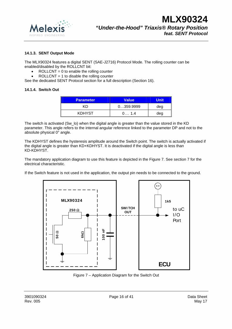
See the dedicated SENT Protocol section for a full description (Section 16). 14.1.4. Switch Out
Parameter Value Unit KD 0…359.9999 deg
KDHYST 0 … 1.4 deg The switch is activated (Sw_lo) when the digital angle is greater than the value stored in the KD parameter. This angle refers to the internal angular reference linked to the parameter DP and not to the absolute physical 0° angle. The KDHYST defines the hysteresis amplitude around the Switch point. The switch is actually activated if the digital angle is greater than KD+KDHYST. It is deactivated if the digital angle is less than KD-KDHYST. The mandatory application diagram to use this feature is depicted in the Figure 7. See section 7 for the electrical characteristic. If the Switch feature is not used in the application, the output pin needs to be connected to the ground.
Figure 7 – Application Diagram for the Switch Out
SWITCHOUT
1k5
5 V
ECU
to uCI/OPort
50 Ω
250 Ω
6kΩ
100
nF
MLX90324

MLX90324 “Under-the-Hood” Triaxis® Rotary Position
feat. SENT Protocol
3901090324 Page 17 of 41 Data Sheet Rev. 005 May 17
14.2. Output Transfer Characteristic There are 2 different possibilities to define the transfer function (LNR):
• With 3 points (defined on X and Y coordinates) and 4 slopes • With 16 points equidistant where only Y coordinates are defined.
Parameter LNR type Value Unit
CLOCKWISE Both 0 CCW 1 CW
DP Both 0 … 359.9999 deg LNR_A_X LNR_B_X LNR_C_X
Only 3 pts 0 … 359.9999 deg
LNR_A_Y LNR_B_Y LNR_C_Y
Only 3 pts 0 … 100 %
LNR_S0 Only 3 pts 0 … 17 %/deg LNR_A_S LNR_B_S LNR_C_S
Only 3 pts -17 … 0 … 17 %/deg
LNR_Y0 LNR_Y1
… LNR_Y16
Only 16 pts 0 …100 %
CLAMP_LOW Both 0 … 100 %
CLAMP_HIGH Both 0 … 100 % 14.2.1. CLOCKWISE Parameter The CLOCKWISE parameter defines the magnet rotation direction.
• CCW is the defined by the 1-4-5-8 pin order direction for the SOIC8 package and 1-8-9-16 pin order direction for the TSSOP16 package.
• CW is defined by the reverse direction: 8-5-4-1 pin order direction for the SOIC8 and 16-9-8-1 pin order direction for the TSSOP16 package.
Refer to the drawing in the IMC positioning sections (Section 20.3 and 20.6).

MLX90324 “Under-the-Hood” Triaxis® Rotary Position
feat. SENT Protocol
3901090324 Page 18 of 41 Data Sheet Rev. 005 May 17
14.2.2. Discontinuity Point (or Zero Degree Point) The Discontinuity Point defines the 0° point on the circle. The discontinuity point places the origin at any location of the trigonometric circle. The DP is used as reference for all the angular measurements.
Figure 8 - Discontinuity Point Positioning
14.2.3. 3-Point LNR Parameters
The LNR parameters, together with the clamping values, fully define the relation (the transfer function) between the digital angle and the output signal. The shape of the MLX90324 transfer function from the digital angle value to the output voltage is described by the drawing below. Six segments can be programmed but the clamping levels are necessarily flat. Two, three, or even five calibration points are then available, reducing the overall non-linearity of the IC by almost an order of magnitude each time. Three or five point calibration will be preferred by customers looking for excellent non-linearity figures. Two-point calibrations will be preferred by customers looking for a cheaper calibration set-up and shorter calibration time.
0°
360°
The placement of the discontinuitypoint (0 point) is programmable.
ASlope LNR_A_S
B
C
Slope LNR_B_S
Slope LNR_C_S
Slope LNR_S0
360(Deg.)
Clamping Low
Clamping High
LNR_A_X
LNR_A_Y
LNR_B_Y
LNR_C_Y
CLAMPHIGH
CLAMPLOW0 %
100 %
0 LNR_B_X LNR_C_X

MLX90324 “Under-the-Hood” Triaxis® Rotary Position
feat. SENT Protocol
3901090324 Page 19 of 41 Data Sheet Rev. 005 May 17
14.2.4. 16-Point LNR Parameters The LNR parameters, together with the clamping values, fully define the relation (the transfer function) between the digital angle and the output signal. The shape of the MLX90324 transfer function from the digital angle value to the output voltage is described by the drawing below.
Figure 9 – 16-Point Calibration
14.2.5. CLAMPING Parameters
The clamping levels are two independent values to limit the output voltage range. The CLAMP_LOW parameter adjusts the minimum output voltage level. The CLAMP_HIGH parameter sets the maximum output voltage level. Both parameters have 16 bits of adjustment with a resolution of approximately 0.076 mV. 14.2.6. DEADZONE Parameter The dead zone is defined as the angle window between 0 and 359.9999. When the digital angle lies in this zone, the IC is in fault mode (RESONFAULT must be set to “1” – See 14.6.1).
0%
CLAMPLOW
LNR_Y16
LNR_Y0
LNR_Y1
LNR_Y2
LNR_Y14
LNR_Y15
100%
CLAMPHIGH
∆x∆x∆x∆x ∆x ∆x
360 Deg

MLX90324 “Under-the-Hood” Triaxis® Rotary Position
feat. SENT Protocol
3901090324 Page 20 of 41 Data Sheet Rev. 005 May 17
14.3. Identification
Parameter Value Unit MELEXSID1 MELEXSID2 MELEXSID3
0 … 65535 0 … 65535 0 … 65535
CUSTUMERID1 CUSTUMERID2 CUSTUMERID3
0 … 65535 0 … 65535 0 … 65535
Identification number: 40 bits freely useable by Customer for traceability purpose.
14.4. Sensor Front-End
Parameter Value Unit
HIGHSPEED 0 = Slow mode 1 = Fast mode
MEDIUMSPEED 0 = Slow mode 1 = Medium mode
AGC 0 = disable 1 = enable
VirtualGain 0 … 41
GAINMIN 0 … 41
GAINMAX 0 … 41 14.4.1. HIGHSPEED Parameter The HIGHSPEED and MEDIUMSPEED parameters define the main frequency for the DSP.
• HIGHSPEED = 0, MEDIUMSPEED = 0 select the Slow mode with a 5.5 MHz master clock. • HIGHSPEED = 0, MEDIUMSPEED = 1 select the Medium mode with a 10 MHz master clock. • HIGHSPEED = 1, MEDIUMSPEED = 0 select the Fast mode with a 16 MHz master clock.
For better noise performance, the Slow Mode must be enabled. 14.4.2. AGC and Virtual Gain Parameters The AGC parameter enables the automatic gain control of the analog chain. The AGC loop is based on
(VX)²+ (VY)² = (Amplitude)² = (Radius)² and it targets an amplitude of 90% of the ADC input span. If AGC is “0”, the gain stored in the parameter GAINMIN is used. Melexis strongly recommends to use AGC = 1. Please note that the angular errors listed in the section 10 are only valid if the AGC is activated. AGC avoids also the saturation of the analog chain and the associated linearity error. The current gain (VG) can be read out with the PTC-04 and gives a rough indication of the applied magnetic flux density (Amplitude).

MLX90324 “Under-the-Hood” Triaxis® Rotary Position
feat. SENT Protocol
3901090324 Page 21 of 41 Data Sheet Rev. 005 May 17
14.4.3. GAINMIN and GAINMAX Parameters GAINMIN & GAINMAX define the boundaries within the gain setting (Virtual Gain) is allowed to vary. Outside this range, the output is set in diagnostic low.
14.5. FILTER
Parameter Value Unit FHYST 0 … 11 deg
FILTER 0… 6
FSWAP 0 1
The MLX90324 includes 3 types of filters:
• Hysteresis Filter: programmable by the FHYST parameter • Low Pass FIR Filters controlled with the Filter parameter • Low Pass IIR Filter
Note: if the parameter FSWAP is set to “1”, the filtering is active on the digital angle. If set to “0”, the filtering is active on the output transfer function. 14.5.1. Hysteresis Filter The FHYST parameter is a hysteresis filter. The output value of the IC is not updated when the digital step is smaller than the programmed FHYST parameter value. The output value is modified when the increment is bigger than the hysteresis. The hysteresis filter reduces therefore the resolution to a level compatible with the internal noise of the IC. The hysteresis must be programmed to a value close to the noise level. Please note that for the programmable version, the FHYST parameter is set to 4 by default. If you do not wish this feature, please set it to “0”. 14.5.2. FIR Filters The MLX90324 features 6 FIR filter modes controlled with Filter = 0…5. The transfer function is described below:
in
j
iij
ii
n xaa
y −=
=
∑∑
=0
0
1

MLX90324 “Under-the-Hood” Triaxis® Rotary Position
feat. SENT Protocol
3901090324 Page 22 of 41 Data Sheet Rev. 005 May 17
The characteristics of the filters no 0 to 5 is given in the Table 1.
Filter No (j) 0 1 2 3 4 5 Type Disable Finite Impulse Response
Coefficients a0… a5 N/A 110000 121000 133100 111100 122210 Title No Filter Extra Light Light
90% Response Time 1 2 3 4 4 5 99% Response Time 1 2 3 4 4 5 Efficiency RMS (dB) 0 2.9 4.0 4.7 5.6 6.2 Efficiency P2P (dB) 0 2.9 3.6 5.0 6.1 7.0
Table 1 - FIR Filters Selection Table
Figure 10 - Step Response and Noise Response for FIR (No 3) and FHYST=10
FIR and HYST Filters : Step response Comparative Plot
30000
32000
34000
36000
38000
40000
0 5 10 15 20 25 30Milliseconds
[0..6
5535
] Sca
le
x(n)fir(n)hyst(n)
FIR and HYST Filter : Gaussian white noise response
39800
39850
39900
39950
40000
40050
40100
40150
40200
0 50 100 150
Milliseconds
[0..6
5535
] Sca
le
x(n)fir(n)hyst(n)

MLX90324 “Under-the-Hood” Triaxis® Rotary Position
feat. SENT Protocol
3901090324 Page 23 of 41 Data Sheet Rev. 005 May 17
14.5.3. IIR Filters The IIR Filter is enabled with Filter = 6. The diagram of the IIR Filter implemented in the MLX90324 is given in Figure 11.
Figure 11 - IIR Diagram
Filter No 6
Type 2nd Order Infinite Impulse Response (IIR) Title Medium
90% Response Time 11 Efficiency RMS (dB) 9.9 Efficiency P2P (dB) 12.9
Coefficient A1 26112 Coefficient A2 10752
Table 2 - IIR Filter
The Figure 12 shows the response of the filter to a Gaussian noise.
Figure 12 - Noise Response for the IIR Filter
Z-1
x(n)
Z-1
Z-1
Z-1
y(n)b0 = 1
b1 = 2
b2 = 1
-a1
-a2
IIR Filter - Gaussian White Noise Response
39800
39850
39900
39950
40000
40050
40100
40150
40200
0 50 100 150Time
[0…
6553
5] S
cale
x(n)y(n)
MLX90324 “Under-the-Hood” Triaxis® Rotary Position
feat. SENT Protocol
3901090324 Page 24 of 41 Data Sheet Rev. 005 May 17
14.6. Programmable Diagnostic Settings
Parameter Value Unit
RESONFAULT 0 1
EEHAMHOLE 0 3131h
14.6.1. RESONFAULT Parameter This RESONFAULT parameter enables the soft reset when a fault is detected by the CPU when the parameter is set to 1. By default, the parameter is set to “0” but it is recommended to set it to “1” to activate the self diagnostic modes (See section 15). Note that in the User Interface (MLX90324UI), the RESONFAULT is split in two bits:
• DRESONFAULT: disable the reset in case of a fault. • DOUTINFAULT: disable output in diagnostic low in case of fault.
14.6.2. EEHAMHOLE Parameter The EEHAMHOLE parameter disables the memory recovery (Hamming code) check when a fault is detected by the CRC when it is equal to 3131h. By default the parameter is set to 0 (enable memory recovery).
14.7. Lock
Parameter Value Unit
MLXLOCK 0 1
LOCK 0 1
14.7.1. MLXLOCK Parameter MLXLOCK locks all the parameters set by Melexis. 14.7.2. LOCK Parameter LOCK locks all the parameters set by the user. Once the lock is enabled, it is not possible to change the EEPROM values anymore. Note that the lock bit should be set by the solver function “MemLock”.
MLX90324 “Under-the-Hood” Triaxis® Rotary Position
feat. SENT Protocol
3901090324 Page 25 of 41 Data Sheet Rev. 005 May 17
15. MLX90324 Self Diagnostic The MLX90324 provides numerous self-diagnostic features. Those features increase the robustness of the IC functionality as it will prevent the IC to provide erroneous output signal in case of internal or external failure modes (“fail-safe”).
Action Effect on Outputs Remark ROM CRC Error at start up (64 words including Intelligent Watch Dog - IWD)
CPU Reset (18) Diagnostic low(19) All the outputs are already in Diagnostic low - (start-up)
ROM CRC Error (Operation - Background task)
Enter Endless Loop: - Progress (watchdog Acknowledge) - Set Outputs in Diagnostic low
Immediate Diagnostic low
RAM Test Fail (Start up) CPU Reset Diagnostic low All the outputs are already in Diagnostic low (start-up)
Calibration Data CRC Error (Start-Up)
Hamming Code Recovery Start-Up Time is increased by 3 ms if successful recovery
Hamming Code Recovery Error (Start-Up)
CPU Reset Immediate Diagnostic low See 14.6.2
Calibration Data CRC Error (Operation - Background)
CPU Reset Immediate Diagnostic low
Dead Zone Set Outputs in Diagnostic low. Normal Operation until the “dead zone” is left.
Immediate Diagnostic low Immediate recovery if the “dead zone” is left
ADC Clipping (ADC Output is 0000h or 7FFFh)
Set Outputs in Diagnostic low Normal mode and CPU Reset If recovery
Immediate Diagnostic low
Radius Overflow ( > 100% ) or Radius Underflow ( < 40 % )
Set Outputs in Diagnostic low Normal mode and CPU Reset If recovery
Immediate Diagnostic low (40 % - 100 %) No magnet / field too high See also 14.4.2
Gain Too Low (The current gain code is strictly less than GAINMIN)
Set Outputs in Diagnostic low Normal mode, and CPU Reset If recovery
Immediate Diagnostic low
Gain Too High (The current gain code is strictly greater than GAINMAX)
Set Outputs in Diagnostic low Normal mode, and CPU Reset If recovery
Immediate Diagnostic low
Redundant Temperature Sensor Mismatch
Set Outputs in Diagnostic low Normal mode, and CPU Reset If recovery
Immediate Diagnostic low
DAC Monitor (Digital to Analog converter)
Set Outputs in Diagnostic low. Normal Mode with immediate recovery without CPU Reset
Immediate Diagnostic low
MLX90324 Fault Mode continues… 18 CPU reset means
1. Core Reset (same as Power-On-Reset). It induces a typical start up time. 2. Periphery Reset (same as Power-On-Reset) 3. Fault Flag/Status Lost 4. The reset can be disabled by clearing the RESONFAULT bit (See 14.6.1)
19 Refer to section 7 for the Diagnostic Output Level specifications

MLX90324 “Under-the-Hood” Triaxis® Rotary Position
feat. SENT Protocol
3901090324 Page 26 of 41 Data Sheet Rev. 005 May 17
…MLX90324 Fault Mode
Fault Mode Action Effect on Outputs Remark ADC Monitor (Analog to Digital Converter)
Set Outputs in Diagnostic low. Normal Mode with immediate recovery without CPU Reset
Immediate Diagnostic low ADC Inputs are Shorted
Undervoltage Mode At Start-Up, wait Until VDD > 3V. During operation, CPU Reset after 3 ms debouncing
- VDD < POR level => Outputs high impedance - POR level < VDD < 3 V => Outputs in Diagnostic low.
Firmware Flow Error CPU Reset Immediate Diagnostic low Intelligent Watchdog (Observer)
Read/Write Access out of physical memory
CPU Reset Immediate Diagnostic low 100% Hardware detection
Write Access to protected area (IO and RAM Words)
CPU Reset Immediate Diagnostic low 100% Hardware detection
Unauthorized entry in “SYSTEM” Mode
CPU Reset Immediate Diagnostic low 100% Hardware detection
VDD > 7 V Set Output High Impedance (Analog)
Pull down resistive load => Diag. Low Pull up resistive load => Diag. High(19)
100% Hardware detection
VDD > 9.4 V IC is switched off (internal supply) CPU Reset on recovery
Pull down resistive load => Diag. Low Pull up resistive load => Diag. High
100% Hardware detection
Broken VSS CPU Reset on recovery Pull down resistive load => Diag. Low Pull up resistive load => Diag. High
Pull down load (≤ 10kΩ) to VSS to meet Diag Lo spec < 4% VDD. Trivial
Broken VDD CPU Reset on recovery Pull down resistive load => Diag. Low Pull up resistive load => Diag. High
Trivial Pull up load (≤ 10kΩ) to VPULLUP ≥ VDD to meet Diag Hi spec > 96% VDD.
MLX90324 “Under-the-Hood” Triaxis® Rotary Position
feat. SENT Protocol
3901090324 Page 27 of 41 Data Sheet Rev. 005 May 17
16. SENT (SAE-J2716) Protocol
16.1. Introduction The MLX90324 features an output mode reporting the angular information and other diagnostic information (e.g. CRC) into a SENT telegram compliant with the approved SAE-J2716 Surface Vehicle Information Report. SENT stands for Single Edge Nibble Transmission as the SENT telegram consists into the transmission of 8 Nibbles (1 nibble = 4 bits) in a row, each nibble being coded in a PWM (Pulse Width Modulation) way with reference to the falling edge. The Single Edge Nibble Transmission encoding scheme is intended for use in applications where high resolution sensor data needs to be communicated from a sensor to an Electronic Control Unit (ECU). It is intended as a replacement for the lower resolution methods of 10 bit A/D’s and PWM. SENT is a point-to-point (i.e. it is not a data bus) unidirectional communications scheme from sensor (transmitting device) to controller (receiving device) which does not include a coordination signal from the controller/receiving device. The sensor signal is transmitted as a series of pulses with data measured as falling to falling edge times. Transmission occurs independently of any action of the receiver module, i.e. the transmission does not require a synchronization signal from the receiver module.
16.2. SENT Protocol Definition The encoding scheme consists of a sequence of pulses which is repeatedly sent by the transmitting module. The time granularity of the transmission is defined as the Clock Tick which is specified as follows:
3 µs ≤ Clock Tick ≤ 10 µs Each nibble is defined in a PWM way: • the output is first driven LOW (falling edge) for 5 Clock Ticks, • then driven HIGH for 7 Clock Ticks + n × Clock Ticks where n is the decimal value of the nibble. For a nibble value of 0 (minimum), the output is driven LOW for 5 Clock Ticks then driven HIGH for 7 Clock Ticks. Total period for the shortest nibble (n = 0) is therefore 12 Clock Ticks. See Figure 13. For a nibble value of 15 (maximum), the output is driven LOW for 5 Clock Ticks then driven HIGH for 22 Clock Ticks. Total period for the longest nibble (n = 15) is therefore 27 Clock Ticks. See Figure 14.

MLX90324 “Under-the-Hood” Triaxis® Rotary Position
feat. SENT Protocol
3901090324 Page 28 of 41 Data Sheet Rev. 005 May 17
Figure 13 – Timing Diagram for Nibble Value = 0d
Figure 14 – Timing Diagram for Nibble Value = 15d
Nibble Value Output LOW
(# Clock Ticks) Output HIGH
(# Clock Ticks) Nibble Period
(# Clock Ticks) Decimal (n) Binary 0d 0000b 5 7 12 1d 0001b 5 8 13 2d 0010b 5 9 14 3d 0011b 5 10 15 4d 0100b 5 11 16 5d 0101b 5 12 17 6d 0110b 5 13 18 7d 0111b 5 14 19 8d 1000b 5 15 20 9d 1001b 5 16 21 10d 1010b 5 17 22 11d 1011b 5 18 23 12d 1100b 5 19 24 13d 1101b 5 20 25 14d 1110b 5 21 26 15d 1111b 5 22 27
0 1 2 3 4 5 6 7 8 9 10 11 12 13 14 15 16 17 18 19 20 21 22 23 24 25 26 27 28 29 30 31 32 33 34 35 36
5 Clock Ticks 7 Clock Ticks 5 Clock Ticks
Nibble Value = 0d = 0000b
Falling Edges
Time (Clock Ticks)
Out
put L
evel
High
Low
0 1 2 3 4 5 6 7 8 9 10 11 12 13 14 15 16 17 18 19 20 21 22 23 24 25 26 27 28 29 30 31 32 33 34 35 36
5 Clock Ticks 22 Clock Ticks 5 Clock Ticks
Nibble Value = 15d = 1111b
Falling Edges
Time (Clock Ticks)
Out
put L
evel
High
Low

MLX90324 “Under-the-Hood” Triaxis® Rotary Position
feat. SENT Protocol
3901090324 Page 29 of 41 Data Sheet Rev. 005 May 17
The transmission itself consists of the following sequence: • “Calibration/Synchronization” pulse period 56 Clock Ticks • One "Status and Communication” nibble pulse (Nibble #1) • A sequence of six “Data” nibble pulses (Nibble #2 … #7) • One “Checksum” (CRC) nibble pulse (Nibble #8) Figure 15 shows a single message transmission for which • Nibble #1 = 0d • Nibble #2 = 15d • Nibble #3 = 0d • Nibble #4 = 8d • Nibble #5 = 15d • Nibble #6 = 0d • Nibble #7 = 8d • Nibble #8 = 12d (for example purpose – please note that this nibble may not necessarily match the
CRC definition)
Figure 15 – Single SENT Message Transmission
The transmission delay of one message depends on the content of the nibbles but the minimum and maximum boundaries are 152 Clock Ticks (456 µs if Clock Tick = 3 µs) and 272 Clock Ticks (816 µs if Clock Tick = 3 µs). The “Calibration/Synchronization” pulse period is measured by the receiver in order to calculate the actual duration of the Clock Tick. In this way, the frequency variations of the main oscillator at the transmitter (i.e. the sensor) can be compensated. The allowable frequency variation is ± 20%. The “Status and Communication” nibble is used to transmit internal status or diagnostic information. The content varies according to the SENT implementation (see Section 16.3 for the implemented SENT version of MLX90324). The “Checksum” nibble contains a 4 bit CRC of the Data nibbles only. The “Status and Communication Nibble” is not included in the CRC calculation. The CRC is calculated using polynomial x4 + x3 + x2 + 1 with seed value of 0101.
10
5 Ticks
Time (Clock Ticks)
Out
put L
evel
High
Low0 20 30 40 50 7060 80 90 100110120130140150
170160
180190200210220230240250
270260
280290300310
51 Ticks
Synchro-
nizationP
ulse
Nibble #1
Nibble #2
Nibble #3
Nibble #6
Nibble #4
Nibble #5
Nibble #7
Nibble #8
0 15 0 8 15 0 8 12
Synchro-
nizationP
ulse
56 Ticks

MLX90324 “Under-the-Hood” Triaxis® Rotary Position
feat. SENT Protocol
3901090324 Page 30 of 41 Data Sheet Rev. 005 May 17
16.3. SENT Protocol Implementation The MLX90324 implements the Single Secure Sensors format described in the Appendix (Section A.3) of SAE-J2716 definition. The Clock Tick is specified at 3 µs. The angular information (12 bits) is spread over 3 data nibbles. A 8-bit rolling counter 0 to 255 with rollover back to 0 is included in 2 data nibbles. The last data nibble is derived from the 1st data nibble including the MSBs (Most Significant Bits) of the computed angle. • Nibble #1 = “Status” Nibble
o When the sensor is determined to be faulted, Bit 0 of the Status Nibble is set to 1 otherwise bit set to 0
o Bit 1, Bit 2 and Bit 3 are set to 0. • Nibble #2 = Angular Information – MSN (Most Significant Nibble) • Nibble #3 = Angular Information – MidN (Middle Nibble) • Nibble #4 = Angular Information – LSN (Least Significant Nibble) • Nibble #5 = 8 bit rolling counter – MSN (Most Significant Nibble) • Nibble #6 = 8 bit rolling counter – LSN (Least Significant Nibble) • Nibble #7 = Inverted copy of Nibble #2 (15 – Nibble #2 value) • Nibble #8 = “Checksum” Nibble The rolling counter can be disabled (to match the “single sensor” format of the Appendix A.4 of the SAE-J2716): in this case, Nibble #5 and Nibble #6 are set to 0. See in the End-User programmable item to see how to disable it (Section 14.1.3)
16.4. Use of the MLX90324 SENT Feature In order to enable the SENT output reporting mode, specific parameters (stored in EEPROM) of the MLX90324 needs to be programmed. While using the Melexis programming tools, the whole operation is actually controlled through a single item as described on Section 14.1.3. The SAE-J2716 recommends a generic application diagram for both the transmitter and the receiver in order to pass the EMC norms, especially the emissions (e.g. radiated emission, conducted emission) requirements. This recommended circuitry applied to the MLX90324LDC (single die – SOIC-8) is shown at the Section 17.4 and MLX90324LGO (dual die – TSSOP-16) is shown at the Section 17.5.

MLX90324 “Under-the-Hood” Triaxis® Rotary Position
feat. SENT Protocol
3901090324 Page 31 of 41 Data Sheet Rev. 005 May 17
17. Recommended Application Diagrams
17.1. Analog Output Wiring with the MLX90324 in SOIC Package
Figure 16 – Recommended wiring for the MLX90324 in SOIC8 package(20).
20 See section 14.1.4 if the Switch Output feature is used.
C2100nF
MLX90324Vdd
NotUsed
Test 2
Vss
1
Test 1 Vdig
Switch Out
Out1
8
4 5
C1100nF
C3100nF
Vdd
GND
Output
5 V
ECU
R110K
C44.7nF
ADC

MLX90324 “Under-the-Hood” Triaxis® Rotary Position
feat. SENT Protocol
3901090324 Page 32 of 41 Data Sheet Rev. 005 May 17
17.2. Analog Output Wiring with the MLX90324 in TSSOP Package
Figure 17 – Recommended wiring for the MLX90324 in TSSOP16 package (dual die).
17.3. PWM Low Side Output Wiring
Figure 18 – Recommended wiring for a PWM Low Side Output configuration(21).
21 See section 14.1.4 if the Switch Output feature is used.
ECU
VDD1
VDD2
GND1GND1
GND2
Vdd1
Vss1
1
Out2
Vdig1
Out1
Vss2
16
8 9
MLX90324
Vdd2
Vdig2
C1100nF
C2100nF
C3100nF
C6100nF
C4100nF
C5100nF
Vdd1GND1
Output1
Vdd2GND2
Output2
ADC
R110K
C74.7nF
R210K
C84.7nF
GND2
C2100nF
MLX90324Vdd
NotUsed
Test 2
Vss
1
Test 1 Vdig
Switch Out
Out1
8
4 5
C1100nF
C34.7nF
Vdd
GND
Output
5 V
ECU
R11K
C44.7nF
Timer5 V
PWM
MLX90324 “Under-the-Hood” Triaxis® Rotary Position
feat. SENT Protocol
3901090324 Page 33 of 41 Data Sheet Rev. 005 May 17
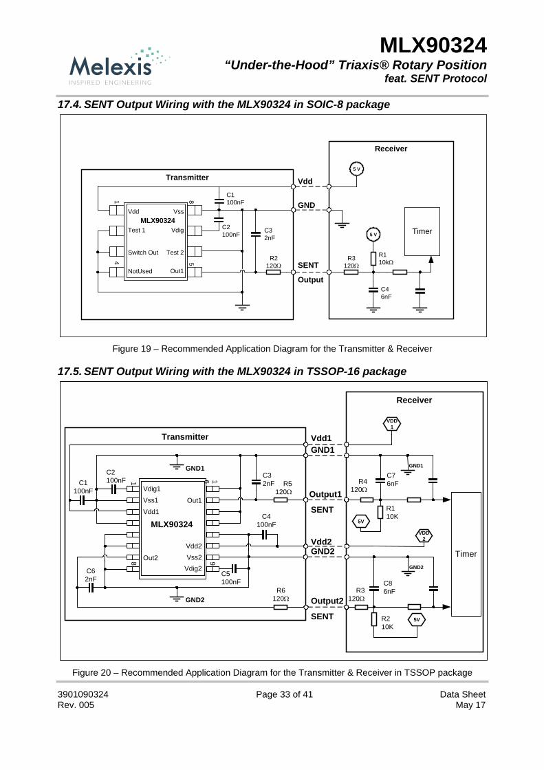
17.4. SENT Output Wiring with the MLX90324 in SOIC-8 package
Figure 19 – Recommended Application Diagram for the Transmitter & Receiver
17.5. SENT Output Wiring with the MLX90324 in TSSOP-16 package
Figure 20 – Recommended Application Diagram for the Transmitter & Receiver in TSSOP package
C2100nF
MLX90324Vdd
NotUsed
Test 2
Vss
1
Test 1 Vdig
Switch Out
Out1
8
4 5
C1100nF
C32nF
Vdd
GND
SENT
5 V
Receiver
R110kΩ
C46nF
Timer
Output
R2120Ω
5 V
R3120Ω
Transmitter
Receiver
VDD1
VDD2
GND1GND1
GND2
Vdd1
Vss1
1
Out2
Vdig1
Out1
Vss2
16
8 9
MLX90324
Vdd2
Vdig2
C1100nF
C2100nF
C32nF
C62nF
C4100nF
C5100nF
Vdd1GND1
Output1
Vdd2GND2
Output2
Timer
R110K
C76nF
R210K
C86nF
GND2
SENT
SENT5V
5V
Transmitter
R5120Ω
R6120Ω
R4120Ω
R3120Ω

MLX90324 “Under-the-Hood” Triaxis® Rotary Position
feat. SENT Protocol
3901090324 Page 34 of 41 Data Sheet Rev. 005 May 17
18. Standard information regarding manufacturability of Melexis products with different soldering processes
Our products are classified and qualified regarding soldering technology, solderability and moisture sensitivity level according to following test methods: Reflow Soldering SMD’s (Surface Mount Devices) • IPC/JEDEC J-STD-020
Moisture/Reflow Sensitivity Classification for Nonhermetic Solid State Surface Mount Devices (classification reflow profiles according to table 5-2)
• EIA/JEDEC JESD22-A113 Preconditioning of Nonhermetic Surface Mount Devices Prior to Reliability Testing (reflow profiles according to table 2)
Wave Soldering SMD’s (Surface Mount Devices) and THD’s (Through Hole Devices) • EN60749-20
Resistance of plastic- encapsulated SMD’s to combined effect of moisture and soldering heat • EIA/JEDEC JESD22-B106 and EN60749-15
Resistance to soldering temperature for through-hole mounted devices Iron Soldering THD’s (Through Hole Devices) • EN60749-15
Resistance to soldering temperature for through-hole mounted devices Solderability SMD’s (Surface Mount Devices) and THD’s (Through Hole Devices) • EIA/JEDEC JESD22-B102 and EN60749-21
Solderability For all soldering technologies deviating from above mentioned standard conditions (regarding peak temperature, temperature gradient, temperature profile etc) additional classification and qualification tests have to be agreed upon with Melexis. The application of Wave Soldering for SMD’s is allowed only after consulting Melexis regarding assurance of adhesive strength between device and board. Melexis recommends reviewing on our web site the General Guidelines soldering recommendation (http://www.melexis.com/Quality_soldering.aspx) as well as trim&form recommendations (http://www.melexis.com/Assets/Trim-and-form-recommendations-5565.aspx). Melexis is contributing to global environmental conservation by promoting lead free solutions. For more information on qualifications of RoHS compliant products (RoHS = European directive on the Restriction Of the use of certain Hazardous Substances) please visit the quality page on our website: http://www.melexis.com/quality.aspx
19. ESD Precautions Electronic semiconductor products are sensitive to Electro Static Discharge (ESD). Always observe Electro Static Discharge control procedures whenever handling semiconductor products.

MLX90324 “Under-the-Hood” Triaxis® Rotary Position
feat. SENT Protocol
3901090324 Page 35 of 41 Data Sheet Rev. 005 May 17
20. Package Information
20.1. SOIC8 - Package Dimensions
20.2. SOIC8 - Pinout and Marking
Marking :
Part Number MLX90324 (3 digits)
324
Die Version (3 digits)
Week Date code (2 digits)Year Date code (2 digits)
YY WW
Not
Use
d
1
8
4
5
324DxxM12345
Xy-E
Sw
itch
Test
0
Vdd
Out
Test
1
Vdi
g
Vss
TOP
Bottom
Dxx
M12345
Split lot number (Optional ) + “-E”Xy-E
Lot number: “M” + 5 digits
0.190.25
NOTES:
All dimensions are in millimeters (anlges in degrees).* Dimension does not include mold flash, protrusions orgate burrs (shall not exceed 0.15 per side).** Dimension does not include interleads flash or protrusion(shall not exceed 0.25 per side).*** Dimension does not include dambar protrusion.Allowable dambar protrusion shall be 0.08 mm total inexcess of the dimension at maximum material condition.Dambar cannot be located on the lower radius of the foot.
5.806.20**
1.27 TYP
4.804.98*
1.521.72
0.1000.250
1.371.57
0.360.46***
3.813.99**
0°8°
0.411.27
MLX90324 “Under-the-Hood” Triaxis® Rotary Position
feat. SENT Protocol
3901090324 Page 36 of 41 Data Sheet Rev. 005 May 17
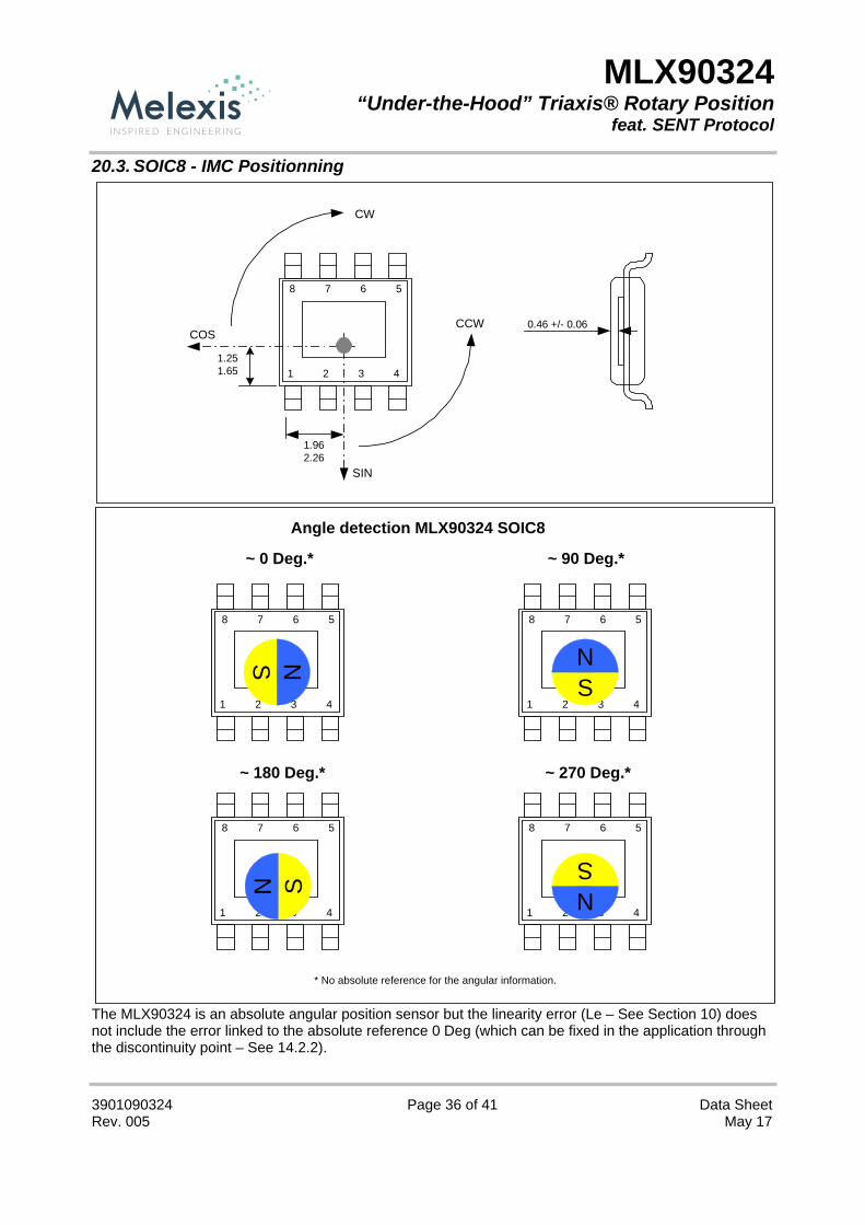
20.3. SOIC8 - IMC Positionning
The MLX90324 is an absolute angular position sensor but the linearity error (Le – See Section 10) does not include the error linked to the absolute reference 0 Deg (which can be fixed in the application through the discontinuity point – See 14.2.2).
0.46 +/- 0.06
1.251.65
1.962.26
1 2 3 4
8 7 6 5
CCW
CW
COS
SIN
Angle detection MLX90324 SOIC8
1 2 3 4
8 7 6 5
~ 0 Deg.*
S
N
1 2 3 4
8 7 6 5
S
N~ 90 Deg.*
1 2 3 4
8 7 6 5
S
N
~ 270 Deg.*
1 2 3 4
8 7 6 5
S
N
~ 180 Deg.*
* No absolute reference for the angular information.
MLX90324 “Under-the-Hood” Triaxis® Rotary Position
feat. SENT Protocol
3901090324 Page 37 of 41 Data Sheet Rev. 005 May 17
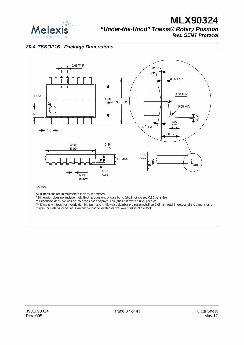
20.4. TSSOP16 - Package Dimensions
0.090.20
1.0 DIA
NOTES:
All dimensions are in millimeters (anlges in degrees).* Dimension does not include mold flash, protrusions or gate burrs (shall not exceed 0.15 per side).** Dimension does not include interleads flash or protrusion (shall not exceed 0.25 per side).*** Dimension does not include dambar protrusion. Allowable dambar protrusion shall be 0.08 mm total in excess of the dimension atmaximum material condition. Dambar cannot be located on the lower radius of the foot.
0.20 TYP
12O TYP
0.09 MIN
0.09 MIN
0.500.75
1.0 TYP
12O TYP
0O
8O
4.905.10*
1.1 MAX
0.050.15
0.850.95
0.190.30***
6.4 TYP4.304.50**
0.65 TYP
1.0
1.0

MLX90324 “Under-the-Hood” Triaxis® Rotary Position
feat. SENT Protocol
3901090324 Page 38 of 41 Data Sheet Rev. 005 May 17
20.5. TSSOP16 - Pinout and Marking
Marking :
Part Number MLX90324 (3 digits)
324
Die Version (3 digits)
Week Date code (2 digits)Year Date code (2 digits)
YY WW
Vdd_1 NotUsed
Test1_1Vss_1
1
Test0_1
Out_2
Vdig_1
Switch_1
Out_1
Vss_2
16
8 9
324Dxx
M12345X
y-E
Test0_2Vdd_2
Switch_2NotUsed
Vdig_2Test1_2
Top
Bottom
Dxx
M12345 Lot number: “M” + 5 digits
Xy-E Split lot number (Optional ) + “-E”
MLX90324 “Under-the-Hood” Triaxis® Rotary Position
feat. SENT Protocol
3901090324 Page 39 of 41 Data Sheet Rev. 005 May 17
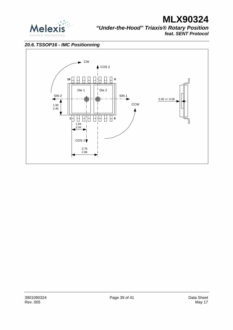
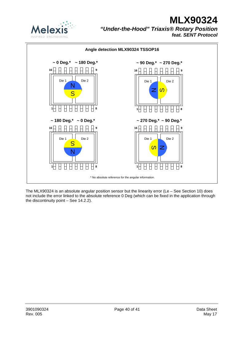
20.6. TSSOP16 - IMC Positionning
0.30 +/- 0.06
1.952.45
1.842.04
2.762.96
1 8
916
CCW
CWCOS 2
COS 1
SIN 2 SIN 1
Die 2Die 1
MLX90324 “Under-the-Hood” Triaxis® Rotary Position
feat. SENT Protocol
3901090324 Page 40 of 41 Data Sheet Rev. 005 May 17
The MLX90324 is an absolute angular position sensor but the linearity error (Le – See Section 10) does not include the error linked to the absolute reference 0 Deg (which can be fixed in the application through the discontinuity point – See 14.2.2).
Angle detection MLX90324 TSSOP16
~ 270 Deg.* ~ 90 Deg.*
1 8
916
Die 2Die 1
S
N
~ 180 Deg.* ~ 0 Deg.*
1 8
916
Die 2Die 1 S
N
~ 0 Deg.* ~ 180 Deg.*
1 8
916
Die 2Die 1
S
N
1 8
916
Die 2Die 1
S
N
~ 90 Deg.* ~ 270 Deg.*
* No absolute reference for the angular information.
MLX90324 “Under-the-Hood” Triaxis® Rotary Position
feat. SENT Protocol
3901090324 Page 41 of 41 Data Sheet Rev. 005 May 17
21. Disclaimer The information furnished by Melexis herein (“Information”) is believed to be correct and accurate. Melexis disclaims (i) any and all liability in connection with or arising out of the furnishing, performance or use of the technical data or use of the product(s) as described herein (“Product”) (ii) any and all liability, including without limitation, special, consequential or incidental damages, and (iii) any and all warranties, express, statutory, implied, or by description, including warranties of fitness for particular purpose, non-infringement and merchantability. No obligation or liability shall arise or flow out of Melexis’ rendering of technical or other services. The Information is provided "as is” and Melexis reserves the right to change the Information at any time and without notice. Therefore, before placing orders and/or prior to designing the Product into a system, users or any third party should obtain the latest version of the relevant information to verify that the information being relied upon is current. Users or any third party must further determine the suitability of the Product for its application, including the level of reliability required and determine whether it is fit for a particular purpose. The Information is proprietary and/or confidential information of Melexis and the use thereof or anything described by the Information does not grant, explicitly or implicitly, to any party any patent rights, licenses, or any other intellectual property rights. This document as well as the Product(s) may be subject to export control regulations. Please be aware that export might require a prior authorization from competent authorities. The Product(s) are intended for use in normal commercial applications. Unless otherwise agreed upon in writing, the Product(s) are not designed, authorized or warranted to be suitable in applications requiring extended temperature range and/or unusual environmental requirements. High reliability applications, such as medical life-support or life-sustaining equipment are specifically not recommended by Melexis. The Product(s) may not be used for the following applications subject to export control regulations: the development, production, processing, operation, maintenance, storage, recognition or proliferation of 1) chemical, biological or nuclear weapons, or for the development, production, maintenance or storage of missiles for such weapons: 2) civil firearms, including spare parts or ammunition for such arms; 3) defense related products, or other material for military use or for law enforcement; 4) any applications that, alone or in combination with other goods, substances or organisms could cause serious harm to persons or goods and that can be used as a means of violence in an armed conflict or any similar violent situation. The Products sold by Melexis are subject to the terms and conditions as specified in the Terms of Sale, which can be found at https://www.melexis.com/en/legal/terms-and-conditions. This document supersedes and replaces all prior information regarding the Product(s) and/or previous versions of this document. Melexis NV © - No part of this document may be reproduced without the prior written consent of Melexis. (2017) ISO/TS 16949 and ISO14001 Certified
For the latest version of this document, go to our website at www.melexis.com
Or for additional information contact Melexis Direct:
Europe, Africa, Asia: America:
Phone: +32 1367 0495 Phone: +1 248 306 5400 E-mail: [email protected] E-mail: [email protected]
ISO/TS 16949 and ISO14001 Certified