final seminar - freddy - itb
DESCRIPTION
This is my final seminar - presentation while I'm doing my research internship at KAIST. Thx to my supervisor : Dr. Isnaeni and Dr. Christophe that help me so much in this presentationTRANSCRIPT

Optimization of ITO annealing and
Color conversion using yellow phosphor for LED Applications
Freddy G. Setiawan
Nano – Bio Photonics Laboratory
(Prof. Cho Yong-Hoon)
Supervised by :Dr. RodriguezDr. Isnaeni
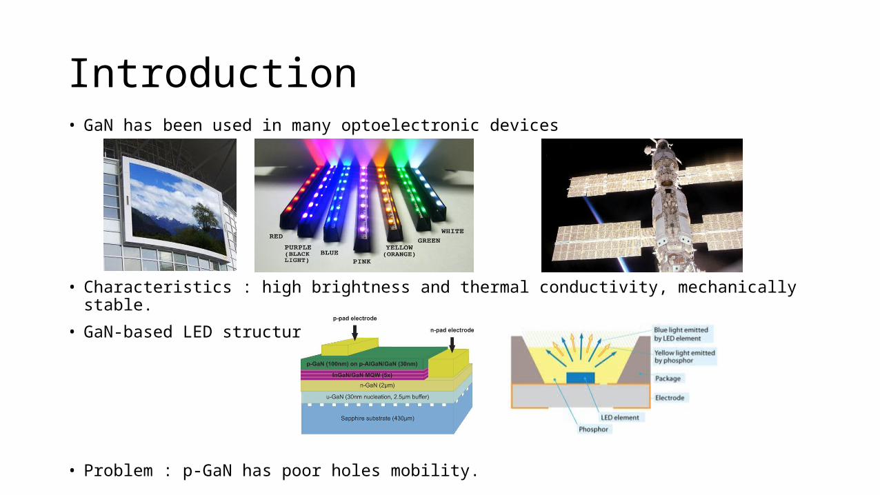
Introduction• GaN has been used in many optoelectronic devices
• Characteristics : high brightness and thermal conductivity, mechanically stable.
• GaN-based LED structure
• Problem : p-GaN has poor holes mobility.

MotivationsWe have high threshold voltage on the IV characteristic of LED with our previous fabrication
process. We suspect the problem comes from ITO annealing.
We have not found the optimum annealing conditions for ITO.For red emission, InGaN has poor efficiency, therefore we use color conversion using phosphor
(red)
We have not known the combination of yellow phosphor material for high color conversion.
Goals
1. Determine the annealing condition for ITO on p-GaN (time & temperature)
2. Determine the composition of coating material (phosphor, epoxy / PR) for high efficiency and color conversion.
Motivations and Goals

Determine the annealing condition for ITO on p-GaN (time & temperature)
1st topic

Schottky vs Ohmic
Metal
𝜙𝑀𝜙𝐵
𝜙𝑆𝜒𝑆
𝐸𝐹
𝐸𝐶
𝐸𝑉
Vacuum
N-Semiconductor
Schottky ContactOhmic Contact
Indium Tin Oxide (ITO) can improve current spreading and transparent to visible light. These characteristics depend on annealing condition[1]
[1] T. Margalith, O. Buchinsky, D. A. Cohen, A. C. Abare, M. Hansen et al. Indium tin oxide contacts to gallium nitride optoelectronic devices. Appl. Phys. Lett. 74, 3930 (1999); doi: 10.1063/1.124227.
Metal
𝐸𝐹
𝐸𝑉
𝐸𝐶𝜙𝑀
𝜙𝑆
N-Semiconductor
Vacuum
𝜒𝑆
09A1 U5 – SPEM (PRT)
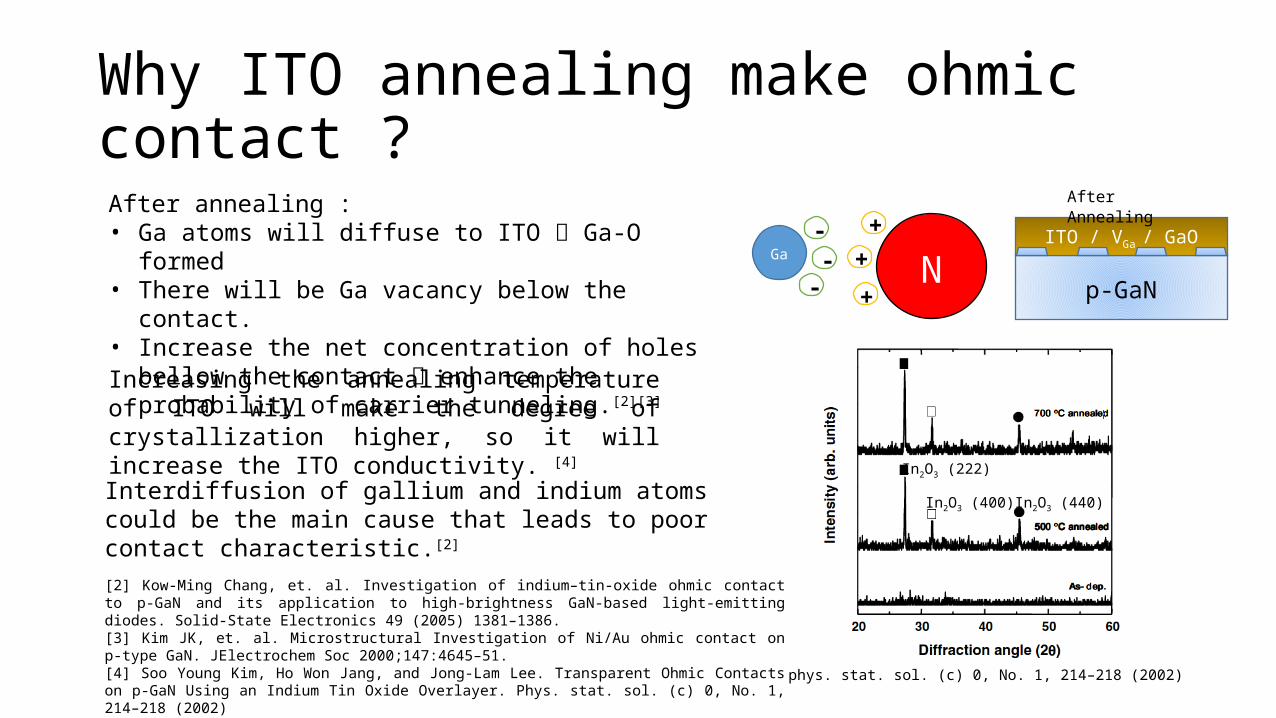
Why ITO annealing make ohmic contact ?
After annealing :• Ga atoms will diffuse to ITO Ga-O formed• There will be Ga vacancy below the contact. • Increase the net concentration of holes bellow the contact
enhance the probability of carrier tunneling.[2][3]
p-GaN
ITO / VGa / GaO
After Annealing
Increasing the annealing temperature of ITO will make the degree of crystallization higher, so it will increase the ITO conductivity. [4]
[2] Kow-Ming Chang, et. al. Investigation of indium–tin-oxide ohmic contact to p-GaN and its application to high-brightness GaN-based light-emitting diodes. Solid-State Electronics 49 (2005) 1381–1386.[3] Kim JK, et. al. Microstructural Investigation of Ni/Au ohmic contact on p-type GaN. JElectrochem Soc 2000;147:4645–51.[4] Soo Young Kim, Ho Won Jang, and Jong-Lam Lee. Transparent Ohmic Contacts on p-GaN Using an Indium Tin Oxide Overlayer. Phys. stat. sol. (c) 0, No. 1, 214–218 (2002)
In2O3 (400) In2O3 (440)
In2O3 (222)
phys. stat. sol. (c) 0, No. 1, 214–218 (2002)
Ga
- -
-
+N +
+
Interdiffusion of gallium and indium atoms could be the main cause that leads to poor contact characteristic.[2]
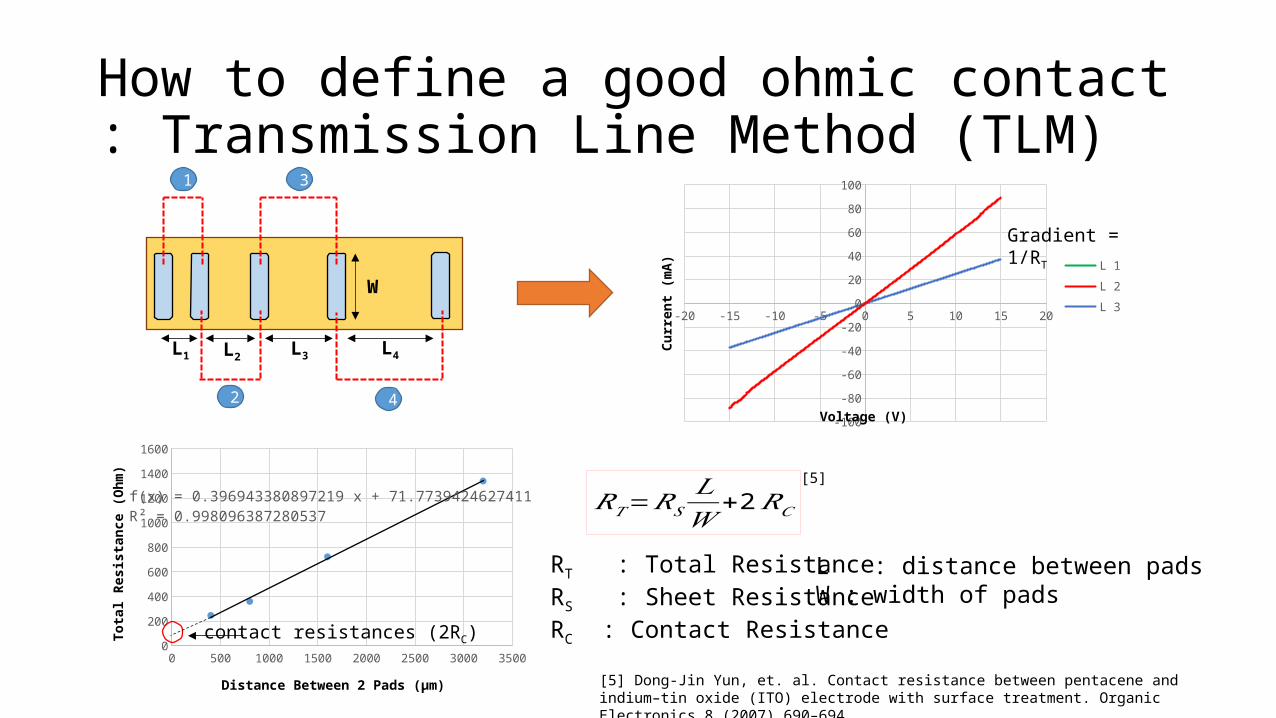
How to define a good ohmic contact : Transmission Line Method (TLM)
L1 L2 L3 L4
1
2
3
4
0 500 1000 1500 2000 2500 3000 35000
200
400
600
800
1000
1200
1400
1600
f(x) = 0.396943380897219 x + 71.7739424627411R² = 0.998096387280537
Distance Between 2 Pads (µm)
Tota
l Res
istan
ce (O
hm)
contact resistances (2RC)
𝑅𝑇=𝑅𝑆𝐿𝑊
+2𝑅𝐶
L : distance between padsW : width of pads
[5]
[5] Dong-Jin Yun, et. al. Contact resistance between pentacene and indium–tin oxide (ITO) electrode with surface treatment. Organic Electronics 8 (2007) 690–694
RT : Total ResistanceRS : Sheet ResistanceRC : Contact Resistance
W-20 -15 -10 -5 0 5 10 15 20
-100
-80
-60
-40
-20
0
20
40
60
80
100
L 1L 2L 3
Voltage (V)
Curr
ent (
mA)
Gradient = 1/RT

Fabrication for TLM Annealing Patterning Etching
• Temperature Dependent200 – 800oC, 15 min
• Time Dependent1 and 15 min, 400oC
LED Structure
ITO
Photoresist DNR
Pre-Bake 110°C for 30s
UV exposure 5s
LED Structure
ITO
Photoresist DNR
Mask
LED Structure
ITO
Photoresist DNR
Developing DPD-200,30s and rinse water
LED Structure
ITOPhotoresist DNR
Etching by Solution :HCl : HNO3: H2O = 50 : 3 : 50
for 2min30s at 50°C
LED Structure
Photoresist DNRITO ITO
Ultrasonification with acetone, 10min
Nitrogen ambient
Soft Bake110°C, 1min30s
Hard Bake110°C, 10min

Fabrication for TLM Annealing Patterning Etching
LED Structure
ITO ITO 100nm
Cross section view
p-GaN
1cm
1mm
ITO
Top view
Results

Temperature Dependence Results
𝑅𝑇=𝑅𝑆𝐿𝑊
+2𝑅𝐶
-10 -8 -6 -4 -2 0 2 4 6 8 10
-100
-75
-50
-25
0
25
50
75
100
50
100
200
400
800
1600
3200
Voltage (V)
Curr
ent (
mA)
-15 -10 -5 0 5 10 15
-1.5
-1
-0.5
0
0.5
1
1.5
5010020040080016003200
Voltage (V)
Curr
ent (
mA)
100 200 300 400 500 600 7000.0
100.0
200.0
300.0
400.0
500.0
600.0
700.0
Temperature (0C)
Cont
act R
esis
tanc
e (o
hm)
200 – 6000C 700 - 8000CDistance between2 pads (µm)
Distance between2 pads (µm)
Temperature200 300 400 500 600
(0C)
Contact Resistance352.3 39.2 38.7 207.6 577.1
(ohm)
240 nm ITO thicknessVan der Pauw measurements

Time Dependence Results
-10 -8 -6 -4 -2 0 2 4 6 8 10
-100
-75
-50
-25
0
25
50
75
100
50
100
200
400
800
1600
3200
Voltage (V)
Curr
ent (
mA)
-15 -10 -5 0 5 10 15
-1.5
-1
-0.5
0
0.5
1
1.5
5010020040080016003200
Voltage (V)
Curr
ent (
mA)
Annealing time : 1 min Annealing time : 15 min
Contact resistance : 1.03 x 10⁴ Ω
Contact resistance : 38.7 Ω
So far, we get the optimum annealing condition for ITO is 4000C for 15 minutes.
Distance between2 pads (µm)
Distance between2 pads (µm)

Determine the composition of coating material (phosphor, epoxy / PR) for high
efficiency and color conversion.
2nd topic

Fabrication of yellow thin film
100 µL epoxy / PR
100 mgyellow phosphor
mixGlass substrate
Thin Film
Blue LED
Spin coatingUV Lamp exposure
2 min
Blue LED
Glass substrateHardened Thin Film
Characterization
LIV SystemSEM & Optical Microscope
drop
or or

330 380 430 480 530 580 630 680 730 7800
0.2
0.4
0.6
0.8
1
1.2
Wavelength (nm)
Rela
tive
Inte
nsity
A1
A2 A3
Color Conversion : =
Power Efficiency : =
Yellow phosphor thin film : best materials
Sample PowerEfficiency
Color Color Position Output
Conversion x y luminescent (lm) power (mW)
Epoxy 57.29% 30.96% 0.2296 0.1951 4.698 22.1447DNR 36.31% 23.31% 0.2277 0.1858 3.4477 16.9728A6 59.13% 34.59% 0.2422 0.2199 5.1387 22.0212
350 400 450 500 550 600 650 700 750 800 8500
0.1
0.2
0.3
0.4
0.5
0.6
EpoxyA6DNR-L300-40
Wavelength (nm)
Rela
tive
Inte
nsit
y
541 – 556 nm
456 nm
epoxy DNR A6 Surface :epoxy A6DNR
20 µm 20 µm 20 µm
---- Blue LED
---- Sample

50 100 150 200 250 300 350 400 450 5000
0.1
0.2
0.3
0.4
0.5
0.6
0.7
0.8
0.9
1
Thickness (um)
Transmission
Fitting TransmissionAbsorption
Fitting Absorption
Yellow phosphor thin film : effective thickness
asymptotic
𝑇=𝐼 (𝑧)𝐼 0
=𝑒−𝛼 𝑧
𝑓 (𝑥 )=exp (−0.05947𝑥 )+0.01534
Penetration depth = 16 µm
0 200 400 600 800 1000 1200
-100
0
100
200
300
400
500
600
700
Wavelength (nm)
Rela
tive
Inte
nsit
y
We choose 100 µm as most effective thickness

0 10 20 30 40 50 60 70 8020.00%
25.00%
30.00%
35.00%
40.00%
45.00%
50.00%
55.00%
60.00%
Current (mA)
Perc
enta
ge
Yellow phosphor on top blue LED
300 400 500 600 700 800 9000
0.1
0.2
0.3
0.4
0.5
0.6
0.72.5 mA5 mA10 mA20 mA40 mA80 mA
Wavelength (nm)
Rela
tive
Inte
nsit
y
456 nm
545 - 560 nm
---- sample 1
---- sample 2
---- sample 3
---- sample 4
Power efficiency
Color Conversion
133.62 µm
500 µm
Blue LED
500 µm
212.81 µm
(1)
500 µm
291.99 µm
(2)
500 µm
321.69 µm
(3)
500 µm150.94 µm
(4)

Conclusions• Experiment on ITO annealing and yellow phosphor color conversion has been conducted.
• So far, the optimum condition for ITO annealing is 4000C for 15 minutes.
• The best combination for phosphor materials are yellow phosphor with epoxy, with 100 µm as the most effective thickness.
0 200 400 600 800 1000 1200-1000
100200300400500600700
Wavelength (nm)
Rela
tive
Inte
nsit
y
100 200 300 400 500 600 7000.0
100.0200.0300.0400.0500.0600.0700.0
Temperature (0C)
Cont
act R
esis
tanc
e (o
hm)

Thank YouFor
Your Attention