finfet cell library design and characterization by manoj
TRANSCRIPT

FinFET Cell Library Design and Characterization
by
Manoj Vangala
A Thesis Presented in Partial Fulfillment
of the Requirements for the Degree
Master of Science
Approved July 2017 by the
Graduate Supervisory Committee:
Lawrence Clark, Chair
John Brunhaver
David Allee
ARIZONA STATE UNIVERSITY
August 2017

i
ABSTRACT
Modern-day integrated circuits are very capable, often containing more than a
billion transistors. For example, the Intel Ivy Bridge 4C chip has about 1.2 billion
transistors on a 160 mm2 die. Designing such complex circuits requires automation.
Therefore, these designs are made with the help of computer aided design (CAD) tools. A
major part of this custom design flow for application specific integrated circuits (ASIC) is
the design of standard cell libraries. Standard cell libraries are a collection of primitives
from which the automatic place and route (APR) tools can choose a collection of cells and
implement the design that is being put together. To operate efficiently, the CAD tools
require multiple views of each cell in the standard cell library. This data is obtained by
characterizing the standard cell libraries and compiling the results in formats that the tools
can easily understand and utilize.
My thesis focusses on the design and characterization of one such standard cell
library in the ASAP7 7 nm predictive design kit (PDK). The complete design flow, starting
from the choice of the cell architecture, design of the cell layouts and the various decisions
made in that process to obtain optimum results, to the characterization of those cells using
the Liberate tool provided by Cadence design systems Inc., is discussed in this thesis. The
end results of the characterized library are used in the APR of a few open source register-
transfer logic (RTL) projects and the efficiency of the library is demonstrated.

ii
ACKNOWLEDGMENTS
Foremost, I would like to sincerely thank my advisor Dr. Lawrence T. Clark for all
the guidance and inspiration throughout the course of my masters’ thesis. I really appreciate
everything he has done for my graduate study during my masters’ program. I would also
like to extend my gratitude to my committee members Dr. John Brunhaver and Dr. David
Allee for their help and guidance.
I would also like to express my special thanks to the members of the Clark-Allee
lab, Vinay Vashishtha, Chandrasekaran Ramamurthy, Anant Mithal, Sai Bharadwaj
Medapuram, Ankita Dosi, Lovish Masand and Parshant Rana for their help and support
throughout my course. This work would not have been possible without their support.

iii
TABLE OF CONTENTS
LIST OF TABLES ............................................................................................................ vii
LIST OF FIGURES .......................................................................................................... vii
CHAPTER
1. INTRODUCTION TO STANDARD CELL LIBRARIES .......................................... 1
1.1 Introduction ........................................................................................................... 1
1.2 Design Flow Using Standard Cell Libraries ......................................................... 2
1.3 Introduction To 7 nm PDK ................................................................................... 2
1.4 Components of A Standard Cell Library .............................................................. 3
1.4.1 Schematic Views of The Cells ............................................................... 3
1.4.2 Layout Views of The Cells ..................................................................... 4
1.4.3 Symbol Views of The Cells .................................................................... 5
1.4.4 Abstract Data/View of The Cells ........................................................... 5
1.4.5 Verilog Definition of The Cells .............................................................. 5
1.4.6 Functionality, Timing, Power and Signal Integrity Data of The Cell .... 6
1.5 Required Cells in A Standard Cell Library .......................................................... 6
1.5.1 Combinational Logic Cells ..................................................................... 6
1.5.2 Sequential Cells ...................................................................................... 7
1.5.3 Buffers and Inverters .............................................................................. 7
1.5.4 Integrated Clock Gaters .......................................................................... 7
1.5.5 Filler and De-Cap Cells .......................................................................... 8
1.6 Characterization of Standard Cell Libraries ......................................................... 8
2. BACKGROUND AND LITERATURE SURVEY ................................................... 10
Page
iv
CHAPTER Page
2.1 Introduction to FinFETs ...................................................................................... 10
2.2 Library Architecture ............................................................................................ 11
2.3 Cell Design .......................................................................................................... 13
2.4 Characterization ................................................................................................... 14
2.5 Library Validation ............................................................................................... 17
3. STANDARD CELL DESIGN .................................................................................... 22
3.1 Number of Cells in A Standard Cell Library ...................................................... 22
3.2 Library Architecture ............................................................................................ 24
3.2.1 Layers ................................................................................................... 24
3.2.2 Cell Height, Gear Ratio and Metal Pitches .......................................... 24
3.3 Layout Design Implications ................................................................................ 26
3.3.1 General Rules for Layout ..................................................................... 26
3.3.2. Fin Cut Implications ............................................................................ 28
3.3.3 M1 Template Usage and M2 Pitch ....................................................... 29
3.3.4 Dummy-Gate Cuts And TDDB ............................................................ 30
3.3.5 Analysis of Stack Nodes ....................................................................... 32
3.3.6 General Structure of Schematic ............................................................ 34
3.3.7 General Structure of a Symbol ............................................................. 35
3.4 Layout View Design Decisions .......................................................................... 35
3.4.1 D-Flip Flop ........................................................................................... 36
3.4.2 Full Adder ............................................................................................. 37
3.4.3 Half Adder ............................................................................................ 39

v
CHAPTER Page
3.4.4 Integrated Clock-Gater ......................................................................... 40
3.4.5 Scan-D-Flip Flop .................................................................................. 42
4. LIBRARY CHARACTERIZATION .......................................................................... 44
4.1 Outline of Library Characterization Flow .......................................................... 44
4.2 CDL And GDS Extraction .................................................................................. 46
4.3 Design Rule Check (DRC) .................................................................................. 48
4.4 Layout Vs Schematic Check (Lvs) ..................................................................... 50
4.5 Abstract Generation ............................................................................................. 51
4.5.1 Significance of LEF File in APR Flow ................................................ 52
4.5.2 LEF File Generation ............................................................................. 53
4.5.3 Scaling the LEF File ............................................................................. 60
4.5.4 Area Attributes Extraction .................................................................... 60
4.5.5 LEF Vt Conversion ............................................................................... 61
4.6 PEX Extraction .................................................................................................... 61
4.7 Liberate Characterization Flow ........................................................................... 63
4.7.1 Liberate Views and Models .................................................................. 64
4.7.1.1 Delay Models ................................................................................. 65
4.7.1.2 Pin Capacitance .............................................................................. 66
4.7.1.3 Constraints ...................................................................................... 67
4.7.1.4 Power Models ................................................................................. 68
4.7.2 Process Corners .................................................................................... 68
4.7.3 Characterization Indices ....................................................................... 69

vi
CHAPTER Page
4.7.4 Liberate Perl Script ............................................................................... 71
5. CONCLUSION ............................................................................................................ 77
REFERENCES ................................................................................................................ 80
APPENDIX
A LIST OF CELLS IN THE STANDARD CELL LIBRARY ...................................... 83
vii
LIST OF TABLES
Table Page
2.1. Number of Cells in Industrial Libraries at Various Nodes ............................. 18
3.1. Pitch and Width of Layers in Standard Cell Library ....................................... 26
3.2. Rise and Fall Delays of NAND5 Obtained from Test Structure .................... 33
5.1. Cell Delay of Cells at Various Corners ........................................................... 77

viii
LIST OF FIGURES
Figure Page
1.1. ASIC Design Flow Using Standard Cells ......................................................... 2
1.2. Schematic of a 2-Input NAND Gate .................................................................. 3
1.3. Layout View of a 2-Input NAND Gate. ............................................................ 4
1.4. Symbol View of a 2-Input NAND Gate ............................................................ 5
2.1. Planar Transistor and a Tri-Gate FinFET Transistor [Bohr11] ...................... 10
2.2 TEM Image of Planar MOSFET And FinFET [Bohr11] ................................ 11
2.3. FEOL And MOL Layers Of (b) [Sherazi16] And (b) [Clark16] .................... 12
2.4. Example of A Current Source Model [Gupta12] ............................................ 16
2.5. Three Schemes of Comparison of Single Paths [Seo08] ................................ 19
2.6. Energy Vs Delay Comparison of The Three Paths in Figure 2.5. [Seo08] .... 20
2.7. Critical Path Delay Comparison of IWLS Benchmarks. [Seo08] .................. 20
3.1. List of Cells Present in The Standard Cell Library ......................................... 23
3.2. Cell Height and Gear Ratio of Standard Cells ................................................. 25
3.3. Layout of A Minimum Sized Inverter ............................................................. 27
3.4. Post-Cut FEOL And MOL Layers of AO21 Standard Cell ............................ 28
3.5. M1 Layout Template ........................................................................................ 30
3.6. Occurrence of TDDB In Post-Cut Fins ........................................................... 30
3.7. With Continuous Dummy Gate (a), Without Continuous Dummy Gate (b).. 31
3.8. NAND5 Schematic (a), Layout with LISD And SDT (b),
Layout with Only SDT (c), Layout with No SDT And LISD (d)................... 32

ix
Figure Page
3.9. Schematic of A Minimum Sized Inverter ........................................................ 34
3.10. Symbol View of a Minimum Sized Inverter ................................................... 35
3.11. D-Flip Flop (DFFHQNx1) Layout .................................................................. 36
3.12. Symmetry of Mirror Adder .............................................................................. 37
3.13. Four Bit Adder Using Full Adder .................................................................... 38
3.14. Full Adder (Fax1) Layout (a), Schematic (b) .................................................. 38
3.15. Logic Level Schematic and Transistor Level Schematic of Half Adder ........ 39
3.16. Layout of Half Adder (HAp5) ......................................................................... 40
3.17. Integrated Clock Gater Logic Level Schematic .............................................. 40
3.18. NAND Gate Implementation Inside the ICGx1 .............................................. 41
3.19. Logic Level Schematic of Scan Flip Flop ....................................................... 42
3.20. Input Stage of a Scan D Flip Flop .................................................................... 43
4.1. Outline of Library Characterization Process ................................................... 45
4.2. Flow Chart Showing of CDL And GDS Extraction Script ............................. 47
4.3. Pseudo Code of The DRC Script ..................................................................... 49
4.4. Pseudo Code of The LVS Check Script .......................................................... 51
4.5 Layout (a) Vs Abstract View (b) Of A Minimum Sized Inverter ................... 52
4.6.1. Opening Library for Abstract Generation ....................................................... 53
4.6.2. Opening Library for Abstract Generation ....................................................... 53
4.6.3. Pin Options Menu ............................................................................................. 54
4.6.4. Pins Menu of Abstract ...................................................................................... 55
4.6.5. Boundary Tab ................................................................................................... 55
x
Figure Page
4.6.6. Extract Menu .................................................................................................... 56
4.6.7. Signal Layer Extraction .................................................................................... 56
4.6.8. Power Layer Extraction .................................................................................... 57
4.6.9. Layer Connectivity Settings ............................................................................. 57
4.6.10 Abstract Settings ............................................................................................... 58
4.6.11. Power Rail Adjustment .................................................................................... 58
4.6.12. Blockage Generation Settings .......................................................................... 59
4.6.13. LEF Export Window ........................................................................................ 59
4.7. Macro Template of a Minimum Sized Inverter ............................................... 60
4.8. Pseudo Code of PEX Extraction Perl Script .................................................... 62
4.9. Input and Output Files for Liberate Characterization ..................................... 64
4.10. NLDM Model (a), CCS Model (b), ECSM Model (c).................................... 66
4.11. Setup Time Calculation (a), Hold Time Calculation (b) ................................. 67
4.12 Ids Vs Vds Curve of a Transistor at Different Temperatures ......................... 69
4.13. Simulation Setup to Find Nominal Slew ......................................................... 70
4.14. Structure of The Library Characterization Script ............................................ 72
4.15 Pseudo Code of The Perl Script to Create the Template File ......................... 73
5.1. AES Core Placed and Routed Using The 7 nm Standard Cell Library .......... 78
5.2. EDAC Design Placed and Routed Using The 7 nm Standard Cell Library ... 78
1
CHAPTER 1
INTRODUCTION TO STANDARD CELL LIBRARIES
1.1 Introduction
In general, large circuits are behaviorally designed and tested (on-the-whole or
block wise) at a high level of abstraction using a hardware description language (HDL) like
Verilog. Hereupon, the behavioral description of the design is synthesized into a logic
netlist using synthesis tools. Then this logic netlist is translated into a geometric netlist
which is placed, routed and optimized using automatic place and route (APR) tools. The
synthesis of behavioral description into logic netlist requires a design environment which
contains descriptions for all the structural logic primitives. These primitives comprise a
base to realize all the required logic functions in the design. The logic netlist generated by
the synthesis tool comprises of a definition of the digital circuit in terms of these structural
units. These units or cells are called the Standard Cells and their collection is called a
Standard Cell Library.
For example, the most basic standard cells are the definitions of NAND, NOR and
INVERTER gates, using which all the combinational circuits can be implemented. Hence
the synthesis tool takes the behavioral description of a combinational circuit and creates a
logic netlist which realizes that behavior using the NAND, NOR and INVERTER cells.
Then these cells can be used as the building blocks to physically create the whole layout
of the combinational circuit.
The quality of any high-level digital design banks on the quality and versatility of
the standard cell libraries used to construct it, hence there is an ongoing need for good cell
libraries in each technology.
2
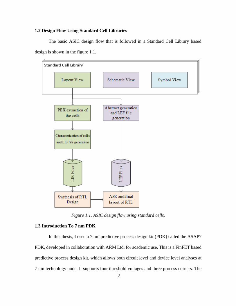
1.2 Design Flow Using Standard Cell Libraries
The basic ASIC design flow that is followed in a Standard Cell Library based
design is shown in the figure 1.1.
Figure 1.1. ASIC design flow using standard cells.
1.3 Introduction To 7 nm PDK
In this thesis, I used a 7 nm predictive process design kit (PDK) called the ASAP7
PDK, developed in collaboration with ARM Ltd. for academic use. This is a FinFET based
predictive process design kit, which allows both circuit level and device level analyses at
7 nm technology node. It supports four threshold voltages and three process corners. The
3
detailed design decisions and process assumptions as well as electrical behavior are
described in [Clark16].
1.4 Components of A Standard Cell Library
The information that a library must contain to be able to implement any ASIC
design completely is:
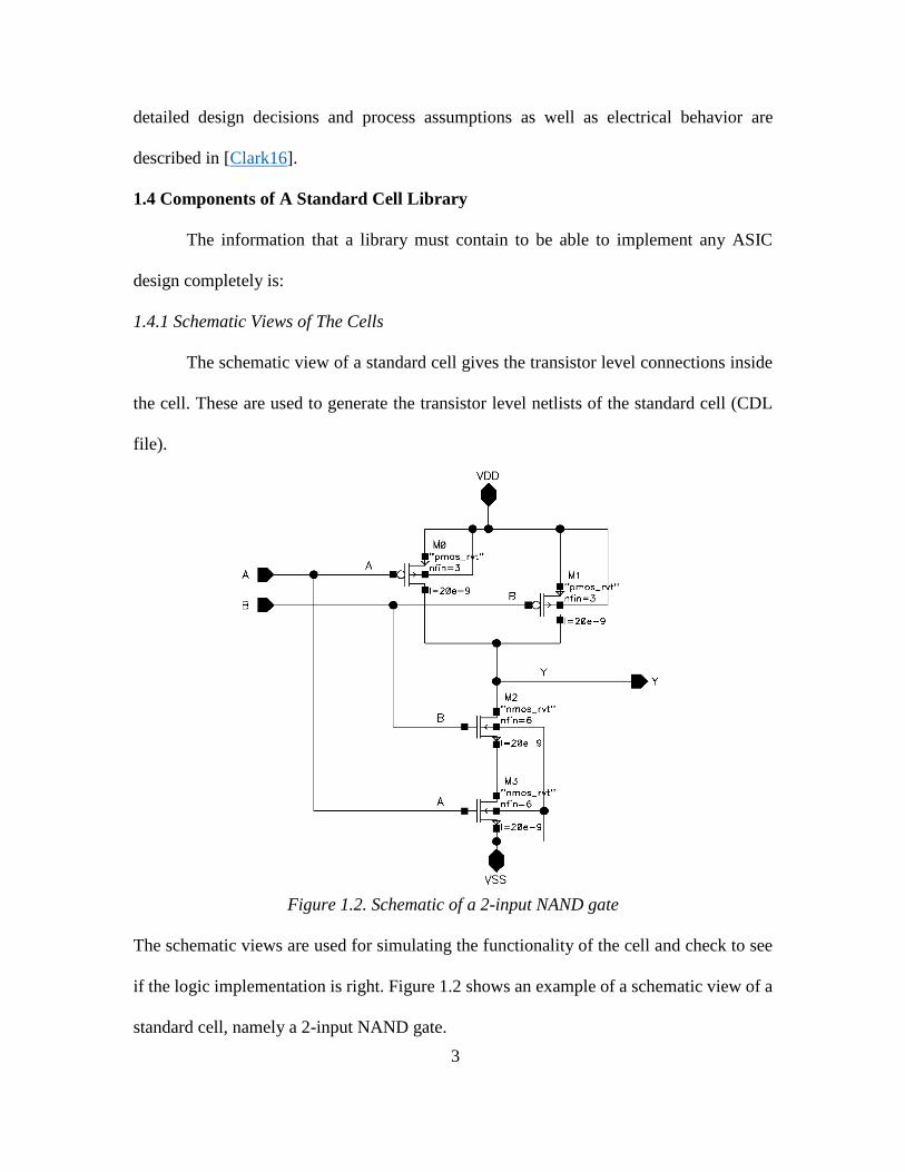
1.4.1 Schematic Views of The Cells
The schematic view of a standard cell gives the transistor level connections inside
the cell. These are used to generate the transistor level netlists of the standard cell (CDL
file).
Figure 1.2. Schematic of a 2-input NAND gate
The schematic views are used for simulating the functionality of the cell and check to see
if the logic implementation is right. Figure 1.2 shows an example of a schematic view of a
standard cell, namely a 2-input NAND gate.
4
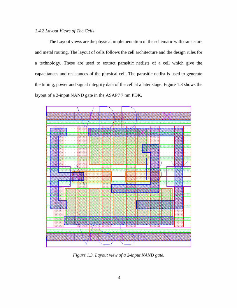
1.4.2 Layout Views of The Cells
The Layout views are the physical implementation of the schematic with transistors
and metal routing. The layout of cells follows the cell architecture and the design rules for
a technology. These are used to extract parasitic netlists of a cell which give the
capacitances and resistances of the physical cell. The parasitic netlist is used to generate
the timing, power and signal integrity data of the cell at a later stage. Figure 1.3 shows the
layout of a 2-input NAND gate in the ASAP7 7 nm PDK.
Figure 1.3. Layout view of a 2-input NAND gate.
5
1.4.3 Symbol Views of The Cells
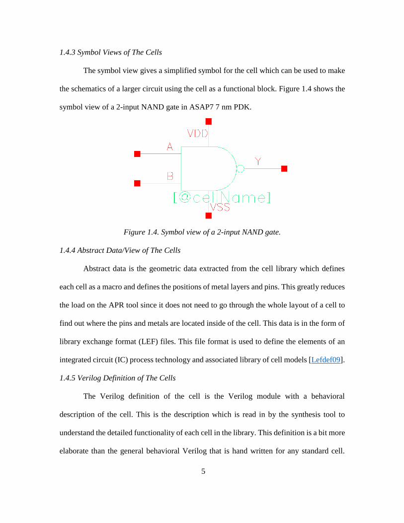
The symbol view gives a simplified symbol for the cell which can be used to make
the schematics of a larger circuit using the cell as a functional block. Figure 1.4 shows the
symbol view of a 2-input NAND gate in ASAP7 7 nm PDK.
Figure 1.4. Symbol view of a 2-input NAND gate.
1.4.4 Abstract Data/View of The Cells
Abstract data is the geometric data extracted from the cell library which defines
each cell as a macro and defines the positions of metal layers and pins. This greatly reduces
the load on the APR tool since it does not need to go through the whole layout of a cell to
find out where the pins and metals are located inside of the cell. This data is in the form of
library exchange format (LEF) files. This file format is used to define the elements of an
integrated circuit (IC) process technology and associated library of cell models [Lefdef09].
1.4.5 Verilog Definition of The Cells
The Verilog definition of the cell is the Verilog module with a behavioral
description of the cell. This is the description which is read in by the synthesis tool to
understand the detailed functionality of each cell in the library. This definition is a bit more
elaborate than the general behavioral Verilog that is hand written for any standard cell.

6
This is due to the breakdown of the function of the cell into various states to make it easy
for the synthesis tool to understand the functionality of the cell precisely.
1.4.6 Functionality, Timing, Power and Signal Integrity Data of The Cell
The functionality, area, timing, power and signal integrity data at a given operating
conditions of the cells are defined in the Synopsys liberty file format. Usually one liberty
file is made for each corner and operating conditions of the library. These files give a
comprehensive view of the performance of each cell, which gives the APR, the tool data
the required to choose between various cells to optimize the performance of the circuit
being designed.
As mentioned above, there are various views of a cell that need to be designed to
make a useful standard cell library. On the other hand, the number of cells and the type of
cells that a standard cell library contains may change depending on the primary purpose of
the library.
1.5 Required Cells in A Standard Cell Library
The cells that are required to make a good standard cell library are described in this
chapter.
1.5.1 Combinational Logic Cells
A standard cell library must be able to realize any logical expression that is
encountered in the synthesis of a design. To accomplish this, combinational logic gates
must be present in the library. Most basic combinational functions like AND, NAND, OR,
NOR and INVERTER must be present in the library since all the logic expressions can be
implemented using these. A versatile standard cell library has various versions of these
cells with different delay, drive strengths, and power consumption parameters. The

7
diversity in terms of these parameters aids in the optimization of the synthesized logic,
since the synthesis tool does this by using the standard cells which fit the exact tradeoff
specification between the cell size and its drive strength. In designs which are optimized
for area, standard cells with smaller size and reasonable drive strength are used at the
expense of higher delay whereas in designs which are optimized for delay, cells with high
drive strength are used at the expense of cell area. Hence by creating various versions of
the same combinational cell, a more efficient design can be achieved.
1.5.2 Sequential Cells
It is mandatory to have sequential cells in a standard cell library which are required
in the synthesis of various synchronous elements of an ASIC design like registers, counters,
queues etc. The most basic sequential cells that are present in any library are D-Latches
and D-Flipflops.
1.5.3 Buffers and Inverters
A cell library must contain various sizes of buffers and inverters so that the delay
elements can be synthesized and to correct various fan out and fan in issues in the design.
The clock tree is synthesized with buffers and inverters; hence they are the cells which are
usually made in a wide range of drive strengths and delay values.
1.5.4 Integrated Clock Gaters
To design any circuits which implement some form of clock gating scheme,
wherein the clock signal is selectively shut off to modules in the design using a clock enable
signal to save power, the standard cell library must contain integrated clock gater cells
since the clock gaters implemented by the synthesis tool from the basic cells have a lot of
delay and area overhead compared to the integrated cells.

8
1.5.5 Filler and De-Cap Cells
Fillers and De-Coupling Capacitance cells (Decap cells) are placed in the empty
space left after the placement and routing of the cells. These cells absorb any glitches and
spikes in the power rails due to their coupling to the signals. They also provide current to
charge the cells in their immediate vicinity when the power rails are farther away and the
speed of circuit operation is very high.
1.6 Characterization of Standard Cell Libraries
In this section, we will discuss the characterization of the standard cells and
generation of the liberty file. The main objective of characterizing a standard cell library is
to obtain the following parameters of each cell in the library:
i. Logic function of the cell
ii. Load capacitances on the inputs and outputs of the cell
iii. Speed of the cell under different input and output conditions (slews and loads)
iv. Power consumption of the cells.
Cell characterization is the process of simulating a standard cell with an analog simulator
or an automated characterization tool to extract this information and convert into a format
that other tools can utilize. Characterization requires; adequate logic, timing, power
consumption for each cell in the library. Cell characterization can be completed by analog
simulation using Spectre/HSPICE simulator, whose output can be evaluated to generate
the timing characterization data or by using an automated tool to tabulate this data.
However, using an automated tool like Cadence Liberate [Lib14] makes the process clean,
easy and error free when setup properly. The tool uses an analog simulator to simulate the

9
design, and wraps up a nice interface to automate the process and give the results in the
standard Synopsys liberty file format.
The characterization of standard cells in Liberate is done by defining timing arcs
and simulating the behavior of the cells in those conditions. A timing arc defines the
propagation of signals through standard cells and defines a timing relationship between
two related pins. These can be divided into delay arcs and constrain arcs. Delay arcs are
used to calculate the parameters like cell delay and clock to Q delay of the standard cells
whereas constraint arcs are used to calculate the parameters like setup time, hold time,
recovery time and removal time. In this thesis, delay is calculated for all cells in the library,
whereas constraints are calculated only for sequential cells because it is quite uncommon
that constraints related to combinational cells, such as minimal pulse width, need to be
characterized.
In further chapters of this thesis, various decisions taken while designing the above-
mentioned components of the standard cell library and the process followed to create the
LEF and liberty files together with the process to automate the flow of extracting the cell
parasitics and to create the collateral for various corners and operating points will be
discussed in detail.
10
CHAPTER 2
BACKGROUND AND LITERATURE SURVEY
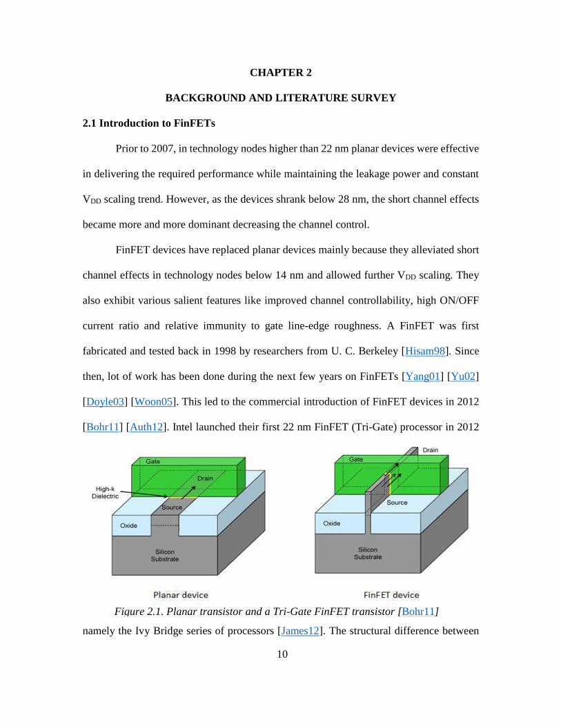
2.1 Introduction to FinFETs
Prior to 2007, in technology nodes higher than 22 nm planar devices were effective
in delivering the required performance while maintaining the leakage power and constant
VDD scaling trend. However, as the devices shrank below 28 nm, the short channel effects
became more and more dominant decreasing the channel control.
FinFET devices have replaced planar devices mainly because they alleviated short
channel effects in technology nodes below 14 nm and allowed further VDD scaling. They
also exhibit various salient features like improved channel controllability, high ON/OFF
current ratio and relative immunity to gate line-edge roughness. A FinFET was first
fabricated and tested back in 1998 by researchers from U. C. Berkeley [Hisam98]. Since
then, lot of work has been done during the next few years on FinFETs [Yang01] [Yu02]
[Doyle03] [Woon05]. This led to the commercial introduction of FinFET devices in 2012
[Bohr11] [Auth12]. Intel launched their first 22 nm FinFET (Tri-Gate) processor in 2012
namely the Ivy Bridge series of processors [James12]. The structural difference between
Figure 2.1. Planar transistor and a Tri-Gate FinFET transistor [Bohr11]

11
FinFET and planar MOSFET is shown in the figures 2.1 and 2.2. In FinFETs, as shown in
the figures, the gate wraps around the fin and hence the channel is controlled from all three
sides. The channel of a FinFET is fully depleted hence offering better control. The FinFETs
modelled in ASAP7 predictive PDK are 32 nm in height and 6.5 nm thick placed on a 27
nm pitch. To allow a grid of 1 nm, fin width is rounded to 7 nm [Clark16].
2.2 Library Architecture
FinFETs have become ubiquitous in the technology nodes below 20 nm. Due to the
introduction of FinFET devices, we see significant changes in the FEOL (Front-End-Of-
Line) and MOL (Middle-Of-Line) layers of the technology node. These changes are also
made keeping the various trade-offs between density, power and drive strength in mind. In
[Sherazi16], the authors have outlined two types of library architectures for the standard
cell libraries at 7 nm and beyond. They present a 9-track architecture and a 7.5 track
architecture with unidirectional metal layers. The 7.5 track architecture is quite like the
architecture of ASAP7 Predictive PDK. Like the MINT (metal-int.) and VINT (via-int.)
Figure 2.2. Transmission Electron Microscope image of (a) 32 nm Planar MOSFET and
(b) 22 nm FinFET [Bohr11]
(a) (b)

12
layers used in [Sherazi16], ASAP7 consists of LIG and LISD layers together with a
bidirectional M1 layer. Since the less number of available metal tracks makes it difficult
for routing the signals inside a standard cell, addition of MINT, VINT layers combined
with M0A (M0-Active) and M0G (M0-Gate) facilitate this intra-cell signal routing. ASAP7
has bidirectional M1 due to the assumed EVU lithography of the layer, and by using the
LIG (Local-Interconnect-Gate) and LISD (Local-Interconnect-Source/Drain) layers along
with the M1, intracell routing is done. The architectural cross section of the layers can be
seen in the figure 2.3.
(a) (b)
Figure 2.3. FEOL and MOL layers of (a) [Sherazi16] and (b) [Clark16]
In [Kaushik12], the authors have presented a comparison between two types of 9-
track library architectures for the 14 nm technology node, one with a unidirectional M1
and one with a bidirectional M1. They benchmarked both the libraries using a 32-bit
multiplier design and based on factors including but not limited to routability, power rail
robustness, colour safe boundary conditions, concluded that the unidirectional library has
lower manufacturing cost and 20% better design efficiency compared to the bidirectional
library, they further stated that by tuning the process specifically for a unidirectional BEOL
(Back-End-Of-Line) layers, unidirectional architecture can be made even more favourable.
On the contrary, at the 14 nm and lower nodes, nine track libraries increase the area of the

13
designs without any significant gain in the speed. This is because of the high drive current
capability of the transistors in these nodes. Hence the logical approach would be to decrease
the number of tracks in standard cells thereby decreasing the device sizes. In such a case,
the aforementioned 20% better design efficiency of the unidirectional library over a bi-
directional library will no longer be valid. Furthermore, in [Kaushik17] the
manufacturability and design efficiency comparison is made against LE3 which demands
very high accuracy in mask positioning and is not preferred due to the high practical
tolerance values.
2.3 Cell Design
The design of cells in a standard cell library involves important decisions and trade-
offs regarding the power, delay and area optimizations. There are many algorithms
available to select the device parameters of a standard cell so that the cell is optimized for
a metric. One such algorithm is outlined in [Singhal06]. Here the authors define a size ratio
for a geometrically sized library assuming that the cells in the library are sized up by a
factor ‘s’ at every step to produce the next larger cell of the same logic. Then, the size ratio
is derived by minimizing the path delays over a test circuit using logical effort. From this,
an upper bound of ‘s’ is derived and for each value of ‘s’ below that value, a library size is
projected and a trade-off is made between library size and loss of speed and performance.
In [Abbas16] the authors have defined an application of mathematical optimization to the
design of standard cells. Here they defined vectors containing various types of parameters,
namely, design parameters (Xd), process parameters (Xs), operating parameters (Xr). These
parameters are mathematically optimized in two parts for decreasing the cost of numerical
simulations: nominal optimization and yield optimization. Here nominal optimization aims

14
at optimally sizing the circuit in nominal process conditions and worst case operating
conditions whereas the yield optimization aims at statistical variation-aware optimal sizing
of circuits in worst-case operating conditions. The problem with the first approach is that
it only optimizes the library for delay and not power consumption and area. Both these
methods are valid mainly for continuously sized standard cell libraries which cannot be
applied for sizing the cells in FinFET libraries where the sizing is discretised. Alongside
the techniques that optimize the library as-a-whole, further optimization techniques are
used in cell libraries with a predetermined use case, as noted from [Golan15] and
[Kaimehr15]. [Golan15] deals with optimizing the flip flops under process variations like
random dopant fluctuation (RDF) and line edge roughness (LER) and run time variations
like bias temperature instability (BTI) by modelling the aging and process variation using
models defined in [Bhardwaj06], [Kuhn11] and using sequential quadratic programming
to increase the reliability of the flip-flop, whereas [Kaimehr15] defines a cell library
optimization technique which predictively sizes the circuits based on the aging factor and
expected lifetime of the cell.
2.4 Characterization
The reliability and accuracy of any design that has been implemented using a
standard cell library is highly dependent on the accuracy with which the standard cells are
characterized, which in-turn depends on the accuracy of estimation of electrical
characteristics of the circuit under realistic nodal voltages and loads. Modelling all the
parameters that affect the operation of a cell and its behaviour is a quite cumbersome task,
undertaking such a task for each individual cell in a standard cell library which at times
may contain several hundreds to thousands of cells is a very resource intensive process. All
15
the past works on library characterization have emphasised proposing ingenious ways to
decrease the computational burden of characterizing the library with little or no
compromise on the accuracy of the results.
The authors of [Cirit91] designed a characterization system using standard UNIX
facilities like sh, awk, ed, sed, cpp etc... It takes the GDSII stream of cells in the library and
a stimuli file as inputs. The stimuli file is processed by cpp before it is handed over to
SPICE. The system measures the parameters like pin capacitances, cell delays, setup and
hold times, current sourcing and sinking capability, logic thresholds, hysteresis of Schmitt
triggers etc. All these measurements can be easily modified as per the requirement of the
characterization. Setup and hold times are calculated using a binary search algorithm which
substantially speeds up the calculation and maintains accuracy. These calculated
parameters are inserted into datasheets using cpp and printed using troff. While primitive,
the basic idea of this kind of characterization system has become the basis of many modern
library characterizers like Cadence Liberate and Cadence Encounter library characterizer
(ELC).
[Lin94] introduces a power dissipation model for a cell based on the
charging/discharging of capacitances at the output node as well as the internal nodes and
capacitance feedthrough effect. This is done by constructing a state transition graph for the
cell to model its behaviour. Then based on the activity factor of the input signals and the
size of transistors, an activity number is derived and assigned to each edge in the graph.
The activity number gives the energy consumption at each edge, whose total sum gives the
total energy consumption of the logic circuit. This method of calculating the power
dissipation is proved to be more than two orders of magnitude faster than the spice
16
simulation and the accuracy is within 10% of it. [Abbas14] defines an accurate and fast
method of calculating the leakage current of a logic cell which iteratively considers the
internal node voltages in the cell. This method is proven to simplify the calculation of
leakage current when variations in supply voltages, loading of output and other complex
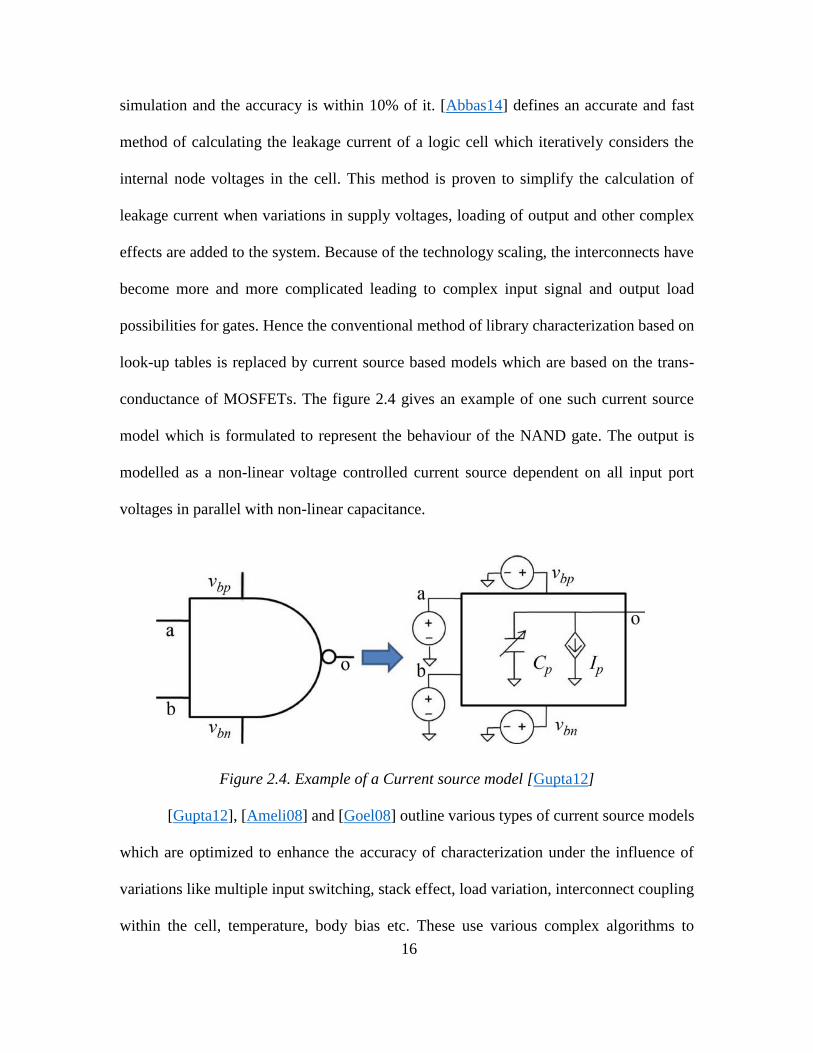
effects are added to the system. Because of the technology scaling, the interconnects have
become more and more complicated leading to complex input signal and output load
possibilities for gates. Hence the conventional method of library characterization based on
look-up tables is replaced by current source based models which are based on the trans-
conductance of MOSFETs. The figure 2.4 gives an example of one such current source
model which is formulated to represent the behaviour of the NAND gate. The output is
modelled as a non-linear voltage controlled current source dependent on all input port
voltages in parallel with non-linear capacitance.
Figure 2.4. Example of a Current source model [Gupta12]
[Gupta12], [Ameli08] and [Goel08] outline various types of current source models
which are optimized to enhance the accuracy of characterization under the influence of
variations like multiple input switching, stack effect, load variation, interconnect coupling
within the cell, temperature, body bias etc. These use various complex algorithms to
17
decrease the overall SPICE simulations required for complete characterization of the
standard cell.
In standard cell libraries, which have a higher percentage of a certain kind of cells,
usage of algorithms and models which make the characterization of those kind of cells
relatively faster and accurate can be a good approach to decrease the overall computational
effort required to characterize the library. [Sharma15] can be viewed as a good example of
such an approach. The authors propose a model for characterizing static D-Latches in the
library which decreases the required SPICE simulations by 67% while losing only an
average accuracy of 1.5%. This model relates the setup time of a latch linearly to the input
transition time and load capacitance. They analyse the effect of variations in process,
voltage and temperature and establish the reliability of the model.
While interesting, since all the modern tools rely on spice-like simulators for
accuracy, the various methods outlined above simplify the process of characterization and
decrease the computational load significantly when the standard cell library consists of
several hundreds or thousands of cells. For ASAP7 standard cell library, the
aforementioned special models and simulators have not been used. The characterization
has been done using HSPICE simulator and composite current models present in Cadence
Liberate. This resulted in very accurate characterization of the standard cells.
2.5 Library Validation
Standard cell libraries in the industry typically contain close to 5000 cells, with
older technologies nodes like 65 nm contain more than 10000 cells.

18
Libraries are designed to have such high number of cells so that when they are used
to place and route a custom design, the synthesis tool can have a very fine grade of control
on the choice of gates it can make depending on the optimization that is being target in the
design. Hence a well-known quality metric of a standard cell library is the performance of
the design which has been placed and routed using that library. It is usually seen that the
cell libraries are benchmarked by using them to place and route well known open source
designs and compared against each other via the speed, power and leakage current values
as demonstrated by the authors of [Xie15]. In custom designs, further optimization can be
achieved by using multiple Vt libraries together to APR (Automatic Place and Route) the
design. [Ghan15] shows one such implementation of a high-level synthesis algorithm. Here
the authors formulated an algorithm which synthesises the given design by assigning all
the paths in the design to high Vt cells initially and then optimizes, by reassigning to low
Vt cells, the individual paths which have timing violations until all the existing slacks in
the design are utilized, leakage power is minimized and the latency constraints are met.
The authors have shown an average improvement of close to 65% in the synthesis run time
and an average improvement of close to 40% in the leakage power consumption compared
to the original designs.
While placing and routing any design using a standard cell library, the synthesis
can be optimized against various metrics like latency, power consumption, signal integrity
etc. This optimization criteria must be given as input to the synthesis tool so that the
Table 2.1 Number of cells in industrial libraries at various nodes [Bittle10]

19
algorithm can choose the suitable standard cells from the single-Vt or multi-Vt library
provided which meet the required specification to achieve those global optimizations. The
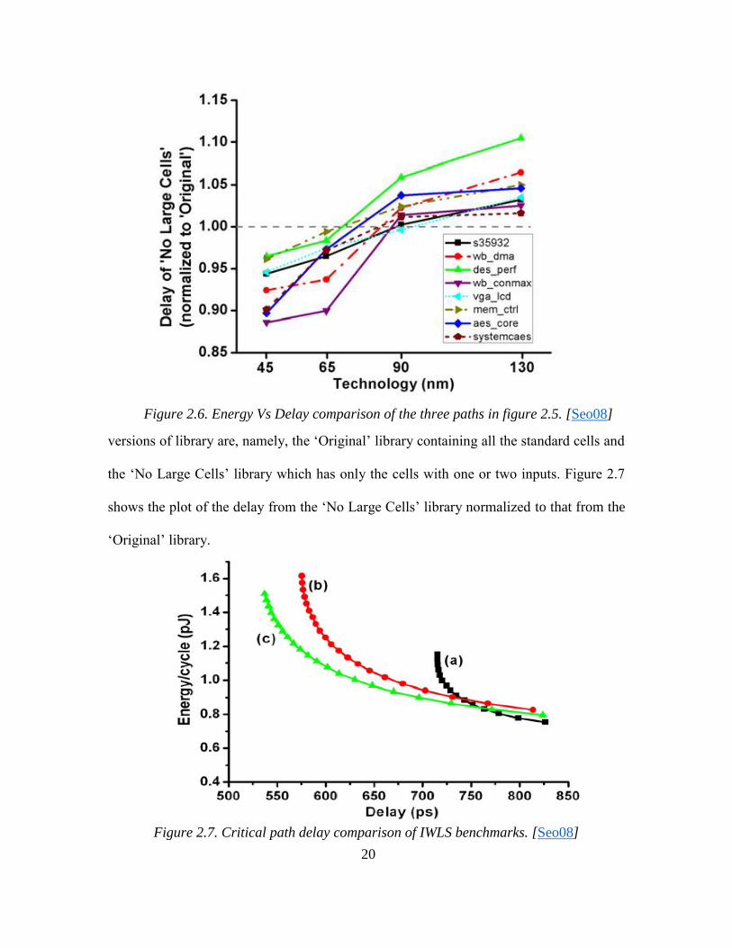
authors of [Seo08] have demonstrated that the presence of large standard cells which have
high number of inputs in the library has become counterproductive since the bulk of critical
path delay in the circuit has shifted from cell delay to interconnect delay. Hence by having
larger cells, the wire length is increased which in-turn increased the delay. The authors
have analysed three single paths and characterized them to demonstrate this effect. The
paths can be seen illustrated in the figure 2.5 and the results of the analysis can be seen in
figure 2.6.
Furthermore, the analysis is extended to the benchmarking designs from [IWLS05]
and the critical path delay is compared between the designs placed and routed by two
versions of the libraries at 130 nm, 90 nm, 65 nm and 45 nm technology nodes. The two
Figure 2.5. Three schemes of comparison of single paths [Seo08]
20
versions of library are, namely, the ‘Original’ library containing all the standard cells and
the ‘No Large Cells’ library which has only the cells with one or two inputs. Figure 2.7
shows the plot of the delay from the ‘No Large Cells’ library normalized to that from the
‘Original’ library.
Figure 2.7. Critical path delay comparison of IWLS benchmarks. [Seo08]
Figure 2.6. Energy Vs Delay comparison of the three paths in figure 2.5. [Seo08]

21
This plot also shows that the normalized delay decreases for the ‘No Large Cells’
library as the technology node becomes smaller and the interconnect starts to dominate the
critical path delay. The notable argument against this analysis is that the delay optimization
has not been carried out properly in the synthesis phase of the ‘Original’ library APR run.
Because, when we consider the 45 nm technology node, while synthesizing the design for
optimized delay, the synthesis algorithm would be able to abstain the use of large cells in
the design if the delay is pushed harder, since the cells required to achieve the delay target
are present in the ‘Original’ library. The algorithm should technically be able to synthesize
the design to match the delay spec of the ‘No Large Cells’ APR run.

22
CHAPTER 3
STANDARD CELL DESIGN
3.1 Number of Cells in A Standard Cell Library
As mentioned in section 1.5, there are various type of cells that a cell library needs
to contain to be able to implement an ASIC design efficiently. But the overall library size
is largely dependent on the design tolerances for delay and power consumption. For the
ASIC designer to be able to optimize the worst-case delay and power consumption of the
design, a standard cell library should contain many different sizes, speeds and drive
strengths of the combinational, sequential or miscellaneous cells to be used in APR of the
design. The authors of [Nguy00] have shown that the improvement in delay between a
standard cell library with 11 cells and a library with 400 cells is just 5% and between a
standard cell library with 20 cells and 400 cells is 2%. On the other hand, the average
increase in area and power when using 11-cell library instead of the 400-cell library is 35%
and 58% respectively and similarly, it is 5% and 17% respectively with a 20-cell library.
This shows that the use of large libraries with more than 10000 cells does not significantly
improve the quality of the design when considering a simple design. Granted that the large
cell libraries can be helpful when carrying out the APR of complex designs with a very
fine requirement on delay, power and area metrics. For simple designs however, using
smaller standard cell libraries not only reduces the cost and time for library generation and
maintenance but also decreases the synthesis time and APR time. Hence the standard cell
library designed using ASAP7 7 nm predictive PDK has 136 standard cells which does not
lead to a great loss in control over the delay, area and power as in the case with 20 cells.
These 136 cells include various drive strengths of sequential cells, combinational cells and
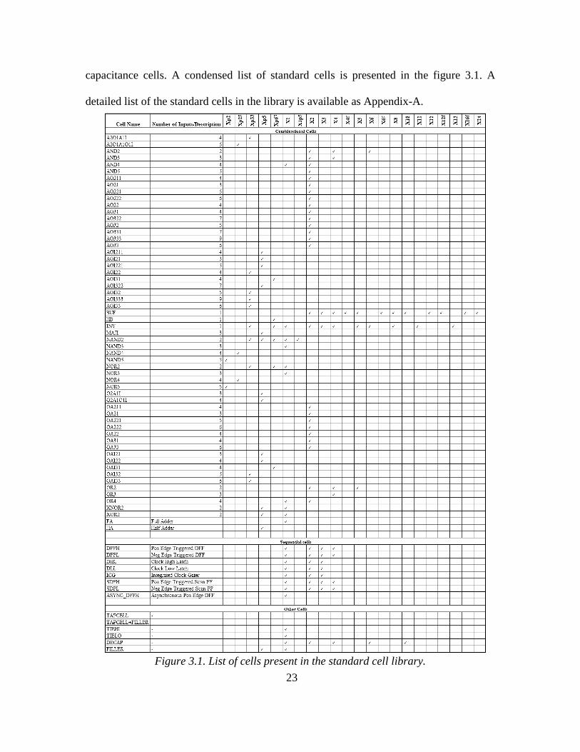
23
capacitance cells. A condensed list of standard cells is presented in the figure 3.1. A
detailed list of the standard cells in the library is available as Appendix-A.
Figure 3.1. List of cells present in the standard cell library.

24
3.2 Library Architecture
A brief introduction to the Library architecture has been given in section 2.2, this
section and the following sections deal with further details of layout architecture of ASAP7
PDK and how they affect the various design decisions taken while creating layout views
for the cells in the library.
3.2.1 Layers
The MOL and FEOL layers of the ASAP7 predictive technology are shown in the
figure 2.3 (b). From this, it can be observed that the metal layers in MOL are divided into
two types, namely local interconnect gate (LIG) and local interconnect source/drain
(LISD). These two metal layers can effectively be used to differentiate the gate and active
connections in standard cells. LISD can cross over the gate layer, hence decreasing the
congestion in the M1 layer for making the important connections within the standard cell.
The BEOL layers of ASAP7 PDK consist of metal layers M1 through M9. Among which,
M1, M2 and M3 allow 2-D routing. Hence M1 can be used for routing inside the standard
cell. While designing the standard cells, utmost care has been taken to use only M1 layer
for intra cell routing. M2 has been used in a few of larger sequential cells but it has been
kept one dimensional with a foresight to make it easy to develop smaller cell height
standard cell libraries with one dimensional M1 and M2, as well as to avoid blocking M2
routing tracks.
3.2.2 Cell Height, Gear Ratio and Metal Pitches
The cell height chosen for the standard cell library is highly dependent on the
applications for which the library would be used. It comes down to the tradeoff between
low power and high performance. Cell height is directly related to the number of fins that

25
a transistor can have in a single device within that height. For libraries requiring higher
drive currents, more fins per device is desirable. The cell height also dictates the number
of metal tracks that can be laid down in the given standard cell height. When this number
is insufficient, complex cells which need more intra cell connections may not be possible
in that standard cell library. The significance of number of metal tracks available for
routing in the standard cell can be quantized using the ratio between the M2 pitch and the
fin pitch. This ratio is called the gear ratio of the library. In this thesis, a gear ratio of 3/4
is used for the standard cell library. Which facilitates various combinations of number of
M2 tracks and fins that can be used, among them, the decision has been made to create the
Figure 3.2. Cell height and Gear ratio of standard
cells.
26
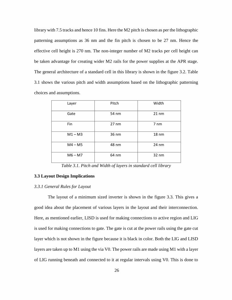
library with 7.5 tracks and hence 10 fins. Here the M2 pitch is chosen as per the lithographic
patterning assumptions as 36 nm and the fin pitch is chosen to be 27 nm. Hence the
effective cell height is 270 nm. The non-integer number of M2 tracks per cell height can
be taken advantage for creating wider M2 rails for the power supplies at the APR stage.
The general architecture of a standard cell in this library is shown in the figure 3.2. Table
3.1 shows the various pitch and width assumptions based on the lithographic patterning
choices and assumptions.
Layer Pitch Width
Gate 54 nm 21 nm
Fin 27 nm 7 nm
M1 – M3 36 nm 18 nm
M4 – M5 48 nm 24 nm
M6 – M7 64 nm 32 nm
Table 3.1. Pitch and Width of layers in standard cell library
3.3 Layout Design Implications
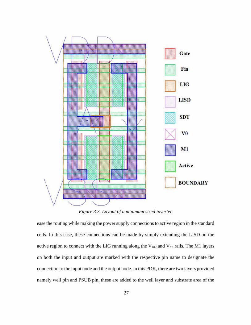
3.3.1 General Rules for Layout
The layout of a minimum sized inverter is shown in the figure 3.3. This gives a
good idea about the placement of various layers in the layout and their interconnection.
Here, as mentioned earlier, LISD is used for making connections to active region and LIG
is used for making connections to gate. The gate is cut at the power rails using the gate cut
layer which is not shown in the figure because it is black in color. Both the LIG and LISD
layers are taken up to M1 using the via V0. The power rails are made using M1 with a layer
of LIG running beneath and connected to it at regular intervals using V0. This is done to
27
ease the routing while making the power supply connections to active region in the standard
cells. In this case, these connections can be made by simply extending the LISD on the
active region to connect with the LIG running along the VDD and VSS rails. The M1 layers
on both the input and output are marked with the respective pin name to designate the
connection to the input node and the output node. In this PDK, there are two layers provided
namely well pin and PSUB pin, these are added to the well layer and substrate area of the
Figure 3.3. Layout of a minimum sized inverter.

28
standard cell. Their purpose is to simplify the LVS and PEX extraction of the cell by
eliminating the need for adding a well tap in the layout.
3.3.2. Fin Cut Implications
In the ASAP7 predictive PDK, the fins are drawn completely across the standard
cell for making it easy to make the layouts, but while manufacturing, they are etched away
wherever the active is not present. Figure 3.4 shows the actual length of the fins that is
retained while manufacturing.
Figure 3.4. Post-Cut FEOL and MOL layers of AO21 standard cell.
From this figure, it can be seen, that the fins are cut half way into the adjacent gate.
Hence when two source/drain regions must be placed beside each other, a diffusion break
must be given to make sure the fins from both the devices do not meet and create a transistor
at that location (as seen from the figure). This double diffusion break is also enforced
29
between one standard cell to another, hence a single gate is placed at both the ends of the
cell called as dummy gate. When two standard cells are abutted, these gates make up the
double diffusion break between them.
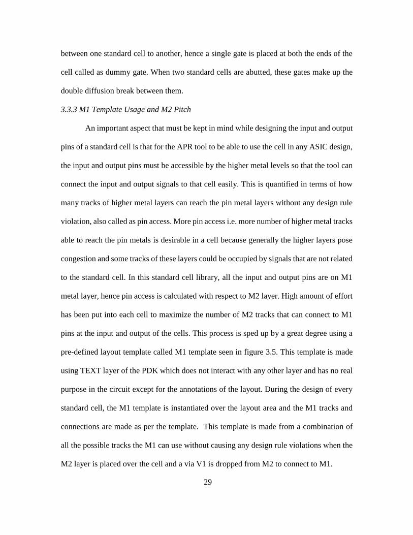
3.3.3 M1 Template Usage and M2 Pitch
An important aspect that must be kept in mind while designing the input and output
pins of a standard cell is that for the APR tool to be able to use the cell in any ASIC design,
the input and output pins must be accessible by the higher metal levels so that the tool can
connect the input and output signals to that cell easily. This is quantified in terms of how
many tracks of higher metal layers can reach the pin metal layers without any design rule
violation, also called as pin access. More pin access i.e. more number of higher metal tracks
able to reach the pin metals is desirable in a cell because generally the higher layers pose
congestion and some tracks of these layers could be occupied by signals that are not related
to the standard cell. In this standard cell library, all the input and output pins are on M1
metal layer, hence pin access is calculated with respect to M2 layer. High amount of effort
has been put into each cell to maximize the number of M2 tracks that can connect to M1
pins at the input and output of the cells. This process is sped up by a great degree using a
pre-defined layout template called M1 template seen in figure 3.5. This template is made
using TEXT layer of the PDK which does not interact with any other layer and has no real
purpose in the circuit except for the annotations of the layout. During the design of every
standard cell, the M1 template is instantiated over the layout area and the M1 tracks and
connections are made as per the template. This template is made from a combination of
all the possible tracks the M1 can use without causing any design rule violations when the
M2 layer is placed over the cell and a via V1 is dropped from M2 to connect to M1.

30
Figure 3.5. M1 layout template.
3.3.4 Dummy-Gate Cuts And TDDB
Time-dependent dielectric breakdown (TDDB) is the phenomenon where a
dielectric undergoes breakdown due to the prolonged exposure of the layer to relatively
low electric field as opposed to immediate breakdown which is caused due to high electric
field. Figure 3.4 shows the extension of fins under the gate. For the fins that are extended
under the gate, if the adjacent active is connected to a VDD signal, the probability of TDDB
occurrence goes high significantly. This is further acerbated in the case of manufacturing
errors like the one shown in the figure 3.6.
Figure 3.6. Occurrence of TDDB in post-cut fins.

31
Due to the manufacturing error, an edge with a high angle is created which
increased the electric field significantly leading to breakdown. This breakdown contributes
to increased gate leakage and reduced life time of the device. Furthermore, when one fin
in the PMOS breaks down, it increased the probability of breakdown of another fin
significantly due to the increased potential on gate. This is shown in the schematic diagram
in figure 3.7.
(a) (b)
Figure 3.7. With continuous dummy gate (a), without continuous dummy gate (b)
To decease the probability of TDDB and to increase the life time of the device, the
dummy gates are cut at the center to disconnect the PMOS and NMOS regions of the date.
This is done using the GCUT layer that is used to cut the gates at the power supplies. Hence
by cutting the dummy gates, the cells in this library provide a longer life time and a lower
susceptibility to TDDB between gate and fin layers.
32
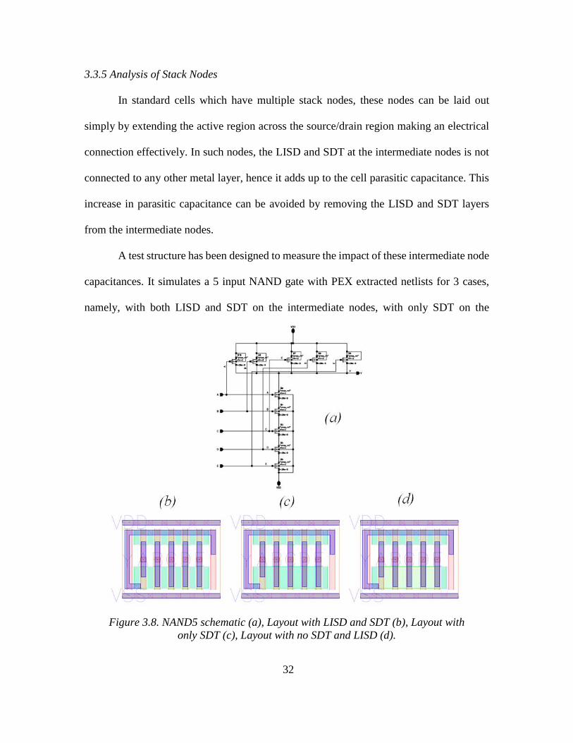
3.3.5 Analysis of Stack Nodes
In standard cells which have multiple stack nodes, these nodes can be laid out
simply by extending the active region across the source/drain region making an electrical
connection effectively. In such nodes, the LISD and SDT at the intermediate nodes is not
connected to any other metal layer, hence it adds up to the cell parasitic capacitance. This
increase in parasitic capacitance can be avoided by removing the LISD and SDT layers
from the intermediate nodes.
A test structure has been designed to measure the impact of these intermediate node
capacitances. It simulates a 5 input NAND gate with PEX extracted netlists for 3 cases,
namely, with both LISD and SDT on the intermediate nodes, with only SDT on the
Figure 3.8. NAND5 schematic (a), Layout with LISD and SDT (b), Layout with
only SDT (c), Layout with no SDT and LISD (d).

33
intermediate nodes and with no LISD and SDT on the intermediate nodes. The rise and fall
times at the intermediate nodes is then tabulated under these three cases. The figure 3.8.,
shows the schematic and layout of the 5 input NAND gate.
Table 3.2. Rise and fall delays of NAND5 obtained from the test structure.
The table 3.2. shows the measured delay values from the simulation. It shows the
percentage increase of delay between the schematic and layout under the three cases
mentioned earlier. From this table, it is clear to see that the percentage change in delay for
the slowest input, i.e., input E on the NAND gate is just 9.68% for rise and 6.86% for delay.
Also, the difference between this metric among the case 1 and case 3 is negligible. Hence,
for standard cell circuits with longer stacks, avoiding the LISD and SDT layer on the
intermediate nodes will result in a small but significant improvement in the delay. Since
the current standard cell library does not have cells with complex stack structures, this
technique is not adopted.
34
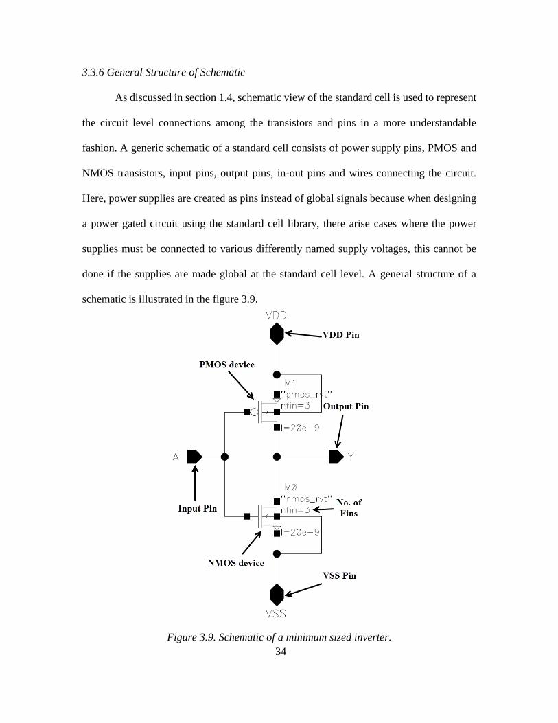
3.3.6 General Structure of Schematic
As discussed in section 1.4, schematic view of the standard cell is used to represent
the circuit level connections among the transistors and pins in a more understandable
fashion. A generic schematic of a standard cell consists of power supply pins, PMOS and
NMOS transistors, input pins, output pins, in-out pins and wires connecting the circuit.
Here, power supplies are created as pins instead of global signals because when designing
a power gated circuit using the standard cell library, there arise cases where the power
supplies must be connected to various differently named supply voltages, this cannot be
done if the supplies are made global at the standard cell level. A general structure of a
schematic is illustrated in the figure 3.9.
Figure 3.9. Schematic of a minimum sized inverter.
35
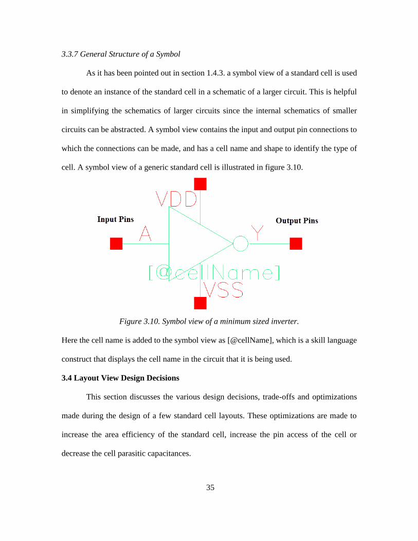
3.3.7 General Structure of a Symbol
As it has been pointed out in section 1.4.3. a symbol view of a standard cell is used
to denote an instance of the standard cell in a schematic of a larger circuit. This is helpful
in simplifying the schematics of larger circuits since the internal schematics of smaller
circuits can be abstracted. A symbol view contains the input and output pin connections to
which the connections can be made, and has a cell name and shape to identify the type of
cell. A symbol view of a generic standard cell is illustrated in figure 3.10.
Figure 3.10. Symbol view of a minimum sized inverter.
Here the cell name is added to the symbol view as [@cellName], which is a skill language
construct that displays the cell name in the circuit that it is being used.
3.4 Layout View Design Decisions
This section discusses the various design decisions, trade-offs and optimizations
made during the design of a few standard cell layouts. These optimizations are made to
increase the area efficiency of the standard cell, increase the pin access of the cell or
decrease the cell parasitic capacitances.
36
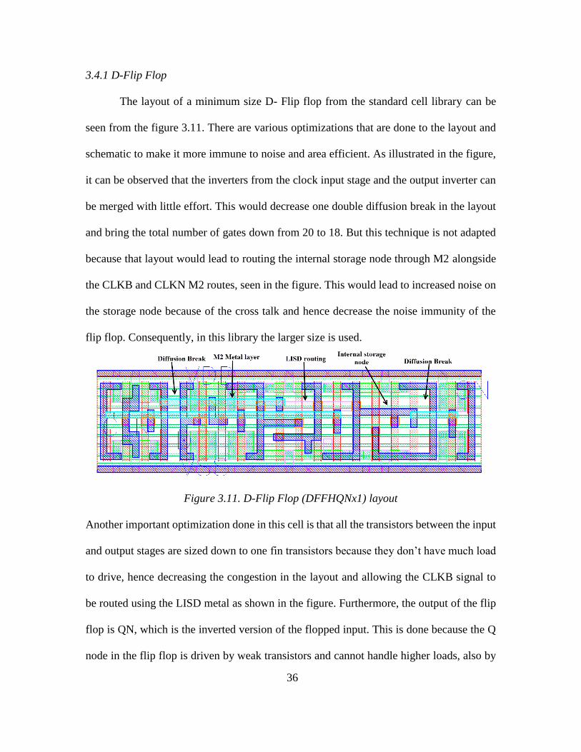
3.4.1 D-Flip Flop
The layout of a minimum size D- Flip flop from the standard cell library can be
seen from the figure 3.11. There are various optimizations that are done to the layout and
schematic to make it more immune to noise and area efficient. As illustrated in the figure,
it can be observed that the inverters from the clock input stage and the output inverter can
be merged with little effort. This would decrease one double diffusion break in the layout
and bring the total number of gates down from 20 to 18. But this technique is not adapted
because that layout would lead to routing the internal storage node through M2 alongside
the CLKB and CLKN M2 routes, seen in the figure. This would lead to increased noise on
the storage node because of the cross talk and hence decrease the noise immunity of the
flip flop. Consequently, in this library the larger size is used.
Figure 3.11. D-Flip Flop (DFFHQNx1) layout
Another important optimization done in this cell is that all the transistors between the input
and output stages are sized down to one fin transistors because they don’t have much load
to drive, hence decreasing the congestion in the layout and allowing the CLKB signal to
be routed using the LISD metal as shown in the figure. Furthermore, the output of the flip
flop is QN, which is the inverted version of the flopped input. This is done because the Q
node in the flip flop is driven by weak transistors and cannot handle higher loads, also by

37
isolating this node from the output using an inverter, the noise on the output node is blocked
from disturbing the feedback loop at the Q node.
3.4.2 Full Adder
The full adder designed in this standard cell library is an implementation of mirror
adder. This adder is optimized to be used when avoiding extra inversions in the logic. It
generates inverted outputs and since the layout is symmetric, it can be used for the
complement circuit. While creating a multi bit adder circuit using this full adder, the
alternating circuits are complemented to create the right output.
(a) (b)
Figure 3.12. Symmetry of mirror adder.
As shown in the figure 3.12 the mirror adder produces the same output even with
its complementary layout, i.e., PMOS and NMOS are interchanged, therefore the adders
shown in 3.12 (a) and 3.12 (b) are equivalent. Hence a multi bit full adder can be made
from this mirror adder as shown in figure 3.13. Here A0-3 and B0-3 are the inputs to the 4-
bit adder, S0-3 are the outputs of the adder and Ci, 0 is the carry input and Co, 3 is the carry

38
output. To obtain the output with proper polarity, alternate, full adder and its complement
are used.
Figure 3.13. Four Bit adder using Full adder.
Here the full adder producing the bits S0 and S2 are the standard cells and the full adder
producing S1 and S3 are the complemented versions. In case of mirror adder, both the adder
and its complement have the same layout. The layout and transistor level schematic are
shown in the figure 3.14.
Figure 3.14. Full adder (FAx1) Layout (a), Schematic (b).
(a)
(b)
39
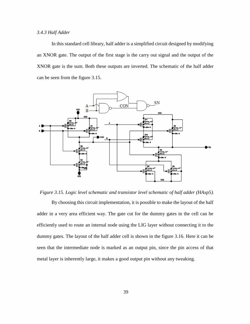
3.4.3 Half Adder
In this standard cell library, half adder is a simplified circuit designed by modifying
an XNOR gate. The output of the first stage is the carry out signal and the output of the
XNOR gate is the sum. Both these outputs are inverted. The schematic of the half adder
can be seen from the figure 3.15.
By choosing this circuit implementation, it is possible to make the layout of the half
adder in a very area efficient way. The gate cut for the dummy gates in the cell can be
efficiently used to route an internal node using the LIG layer without connecting it to the
dummy gates. The layout of the half adder cell is shown in the figure 3.16. Here it can be
seen that the intermediate node is marked as an output pin, since the pin access of that
metal layer is inherently large, it makes a good output pin without any tweaking.
Figure 3.15. Logic level schematic and transistor level schematic of half adder (HAxp5).
40
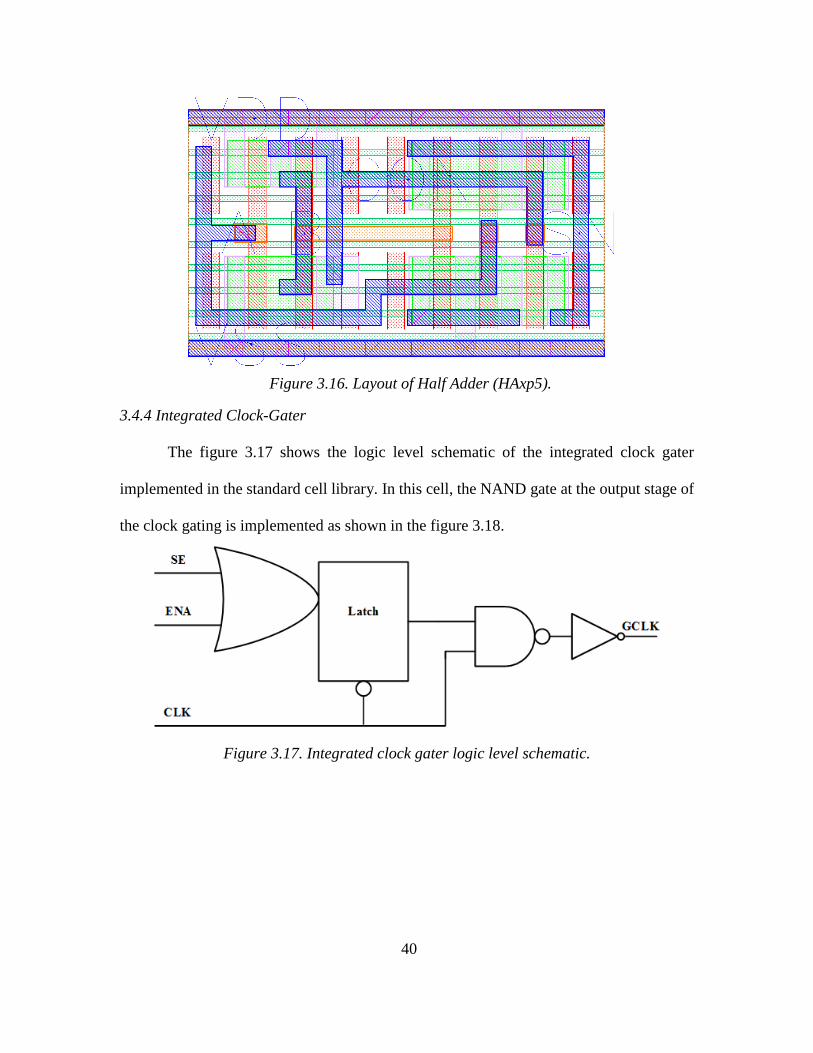
3.4.4 Integrated Clock-Gater
The figure 3.17 shows the logic level schematic of the integrated clock gater
implemented in the standard cell library. In this cell, the NAND gate at the output stage of
the clock gating is implemented as shown in the figure 3.18.
Figure 3.17. Integrated clock gater logic level schematic.
Figure 3.16. Layout of Half Adder (HAxp5).

41
Here the NAND gate is skewed by increasing the PMOS fins from 3 fins to 4 fins. This
way, the even numbered fins can be split into two devices and hence the fin spade can be
used to include two LIG layers in staggered fashion without violating any design rules.
This essentially pushes the supply connected drain/source terminals to both the ends of the
NAND gate hence providing an opportunity to merge those nodes with the supply
connected drain/source nodes of other devices, here, the input and output inverters. By
using this optimization, two diffusion breaks are eliminated from the design making in
compact. On the other hand, the decrease in rise time of the output of NAND gate, is
rectified to an extent by the output inverter and hence does not affect the output by a large
degree.
Figure 3.18. NAND gate implementation inside the ICGx1
42
3.4.5 Scan-D-Flip Flop
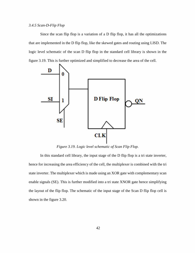
Since the scan flip flop is a variation of a D flip flop, it has all the optimizations
that are implemented in the D flip flop, like the skewed gates and routing using LISD. The
logic level schematic of the scan D flip flop in the standard cell library is shown in the
figure 3.19. This is further optimized and simplified to decrease the area of the cell.
Figure 3.19. Logic level schematic of Scan Flip Flop.
In this standard cell library, the input stage of the D flip flop is a tri state inverter,
hence for increasing the area efficiency of the cell, the multiplexer is combined with the tri
state inverter. The multiplexer which is made using an XOR gate with complementary scan
enable signals (SE). This is further modified into a tri state XNOR gate hence simplifying
the layout of the flip flop. The schematic of the input stage of the Scan D flip flop cell is
shown in the figure 3.20.
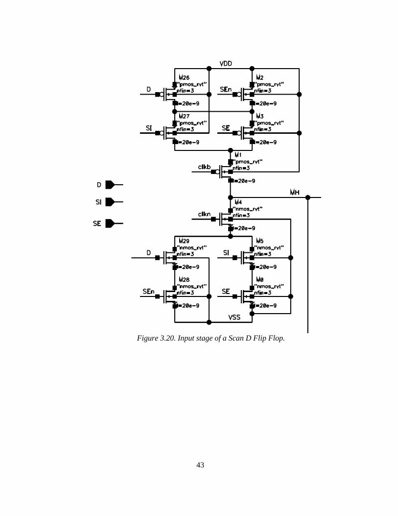
43
Figure 3.20. Input stage of a Scan D Flip Flop.
44
CHAPTER 4
LIBRARY CHARACTERIZATION
Once a standard cell library has been designed, i.e., the layout, schematic and
symbol views of the cells are made, for it to be used in the development of an ASIC design,
certain collateral must be created from the cells. The extraction of required collateral from
the library is called library characterization. In a standard cell based design flow, the APR
is done by EDA applications which go through the properties of all the cells in the library
and make decisions like which cell must be used for a certain logic path in the design, since
the libraries contain large number of cells, calculating the properties of the cells in the APR
stage can be time consuming, hence the library is characterized and the required data is
provided to the EDA tools in the form of standard file formats. Before characterizing a
library, it must be first checked for design rule violations and layout vs schematic matching,
to ensure that there are no errors in the layouts of the library. The following section
discusses about the overall flow of a library characterization process and each one of it will
be dealt with in detail later in the chapter.
4.1 Outline of Library Characterization Flow
The collateral required for proper usage of the library is mainly the LEF files,
liberty files and the schematic netlists (.cdl) and parasitic extracted netlists of the library.
Figure 4.1 shows the whole process of creating these files along with design rule
verification and layout vs schematic matching. This figure does not give a clear idea of the
time line that must be followed for a proper library characterization process. There are
various process decisions involved, which are not shown, for example, PEX extraction and
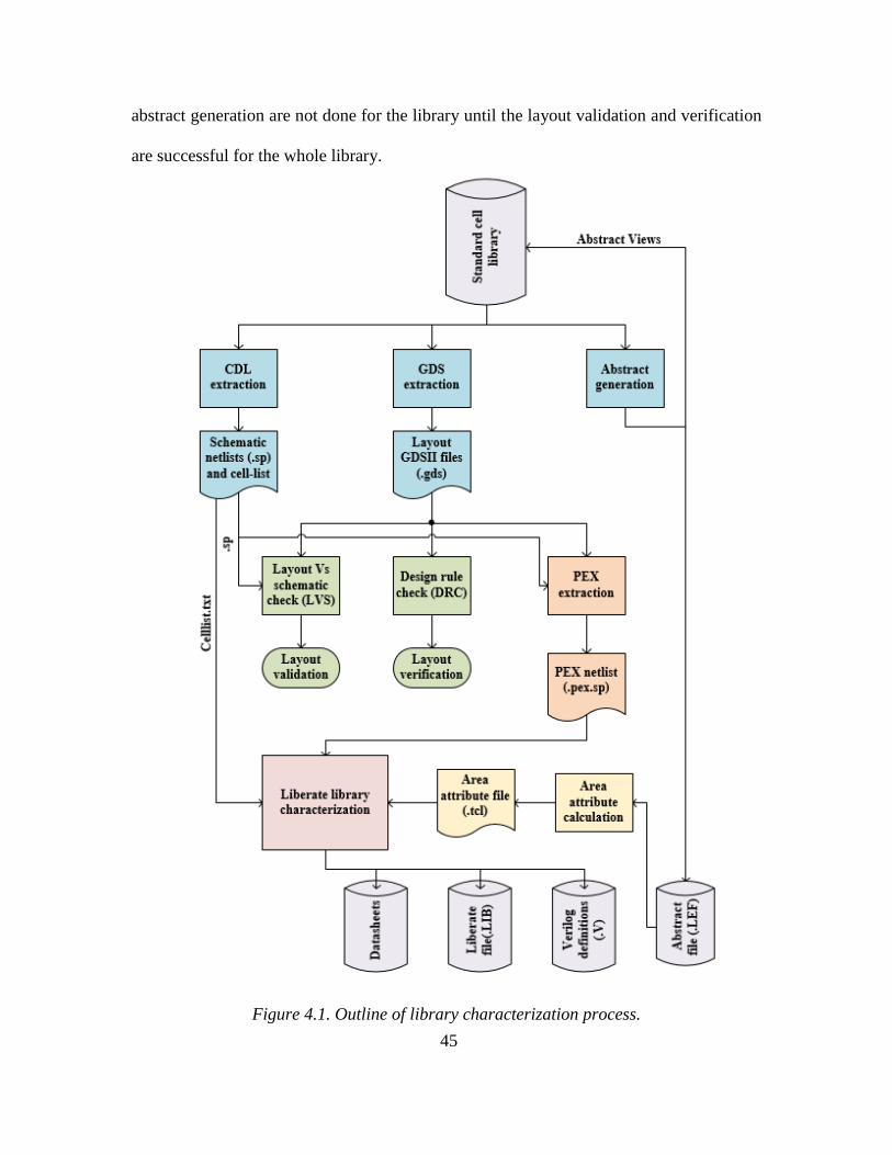
45
abstract generation are not done for the library until the layout validation and verification
are successful for the whole library.
Figure 4.1. Outline of library characterization process.

46
In this thesis, the above process is implemented over the complete library using
Perl scripting. The flow is broken into various sub sections and each sub section is
automated over the complete library using Perl scripts.
4.2 CDL And GDS Extraction
A circuit design language (CDL) netlist gives the description of the circuit of a
standard cell. It is generated from the schematic of the cell and contains the transistor
device definitions and the connections between them. This netlist is used to verify the
layout of the cell against the schematic and to test the functionality of the cell. On the other
hand, GDS stands for graphic database system, which is a file format used to control
integrated circuit photomask plotting. It is a universal exchange format for layout data
between design tools. The standard cell layouts are converted to individual GDS files and
they are used for further processing like PEX extraction or DRC verification.
For a single standard cell, the CDL and GDS can be extracted using the command
interpreter window of virtuoso application, but this is quiet time consuming for a standard
cell library, furthermore, when changes are made for the cell layouts or schematics,
extracting all of them separately adds up exponentially to the design effort, hence to avoid
this, I have written a Perl script which takes in the standard cell library folder and extracts
the CDL and GDS of all the cells in the library. The flow chart depicting the functioning
of the script is shown in the figure 4.2. This script must be run from inside the ASAP run
directory and the .cshrc file must be sourced before running the script because Perl cannot
source the .cshrc file internally. The CDL and GDS extraction script takes the library name
as the argument and has a user input prompt, hence cannot be run in the background. The
general syntax of running the script is “<CDL_GDS_extract.pl> <Library_name>”. It is
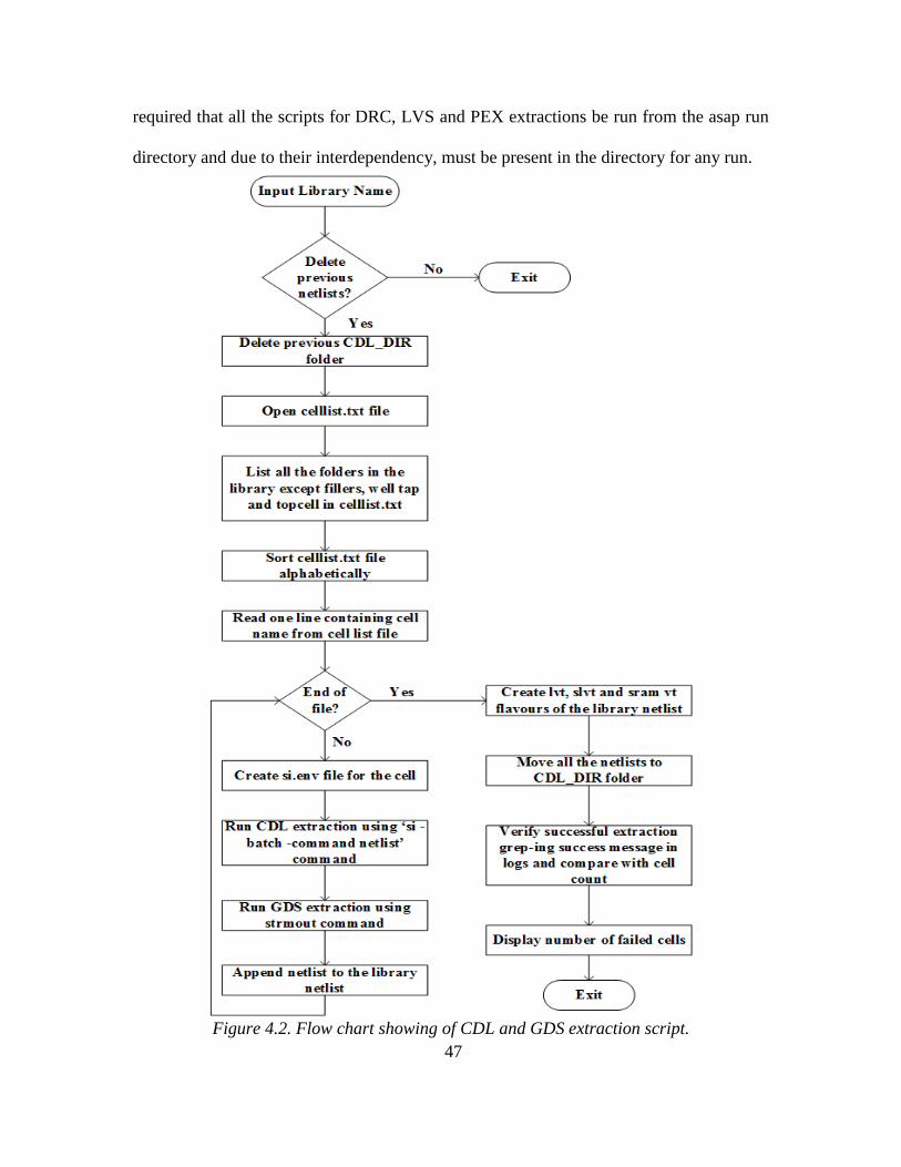
47
required that all the scripts for DRC, LVS and PEX extractions be run from the asap run
directory and due to their interdependency, must be present in the directory for any run.
Figure 4.2. Flow chart showing of CDL and GDS extraction script.
48
This script generates the schematic level netlists and GDS files of individual cells
in the form of <cell_name>. sp and <cell_name>. gds, these can be found inside the
CDL_DIR folder. The overall library netlist which is a concatenation of all the individual
cell netlists is also created in the form of <Library_name>. cdl, furthermore, this netlist is
generated for all the Vt values. The script displays the total number of cells in the library
and total number of cells passing and failing extraction. The celllist.txt file generated by
this script containing the names of all the characterizable cells in the library can be used
for the Liberate characterization run at a later stage to designate which cells among the
library must be characterized.
4.3 Design Rule Check (DRC)
Design rule checking is an important part of library design, it determines whether
the physical layout of the standard cell satisfies a series of design rules which are provided
by manufacturers. These design rules specify the geometric and connectivity restrictions
on the various layers in the layout to account for the process variability of the
semiconductor design process. Similar to the process of CDL and GDS extract, DRC
checking is usually done on individual cells for small libraries, but this approach increased
the design time by a lot, so a Perl script has been written to take advantage of the batch
mode in calibre nmDRC tool by mentor graphics and run the DRC on the complete library
in a single run. The pseudo code of the DRC checking script is shown in the figure 4.3.
Prior to running the script, the .cshrc file has to be sourced and also the variable for the
DRC rule file path has to be updated to point to the latest rule file. This script takes the
name of the library as the input command line argument. In this setup, the latch up errors
in individual standard cells are bound to arise since they are caused due to the lack of a

49
well tap connection in the layout of the cell and they can be safely ignored for the DRC
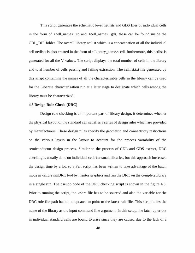
part of the standard cell verification.
Figure 4.3. Pseudo code of the DRC script.

50
This script creates the directory DRC_DIR which consists of individual sub
directories for each cell containing the DRC rule file, log file and summary file. The
complete summary of the DRC errors is found in DRC_Error.log file in DRC_DIR.
4.4 Layout Vs Schematic Check (Lvs)
While a successful DRC signifies the conformance of the layout with the
fabrication design rules, it does not guarantee that the layout represents a circuit same as
the schematic. Since schematics are simulated beforehand and verified functionally, they
are used as the golden model for validating the layouts. This is done through a process
called layout versus schematic (LVS) check. A successful LVS check ensures that the
drawn layout of the standard cell has all the devices and their connections matching that of
the cell’s schematic. This is run using the calibre nmLVS tool provided by mentor graphics.
For a cell to be LVS clean, it is mandatory that the well tap connection be made in the
layout, but while running the LVS on the whole library in batch mode, adding the well tap
connection for each cell and removing it after the LVS check can become a cumbersome
task for large libraries, hence in ASAP7 predictive PDK, two layers are provided, namely,
well pin and PSUB pin, using which the well tap connections can be made without adding
any FEOL or MOL layers to the layout. This tremendously simplifies the task of LVS
checking. The figure 4.4 shows the pseudo code of the Perl script written to run LVS check
on the whole library in batch mode. Similar to DRC check, it takes the name of the standard
cell library as command line argument and prior to running the script, .cshrc file must be
sourced and the variable in the script pertaining to the location of the lvs rule file must be
updated to point to the latest rule file.
51
Figure 4.4. Pseudo code of the LVS check script.
This script generates a directory LVS_DIR which consists of individual sub directories for
each standard cell of the library containing the LVS run log, lvs report, .sp and .gds of the
standard cell.
4.5 Abstract Generation
Abstract view of a standard cell is the simplified layout view of the cell containing
only the data relevant to enable the APR tool to place the cell in a design and connect its
inputs and outputs using higher metal layers at the right point. It does not contain any
device or parasitic data. These views must be generated once the whole library is DRC and
LVS checked and all the layouts are finalized.

52
4.5.1 Significance of LEF File in APR Flow
LEF stands for library exchange format, this file is used to transfer the abstract view
data from the standard cell library to the APR tool. This data is used by the APR tool to
place the cells in the ASIC design, the primary purpose of LEF file is to save valuable
resources of the APR tool by providing only an abstract view of the layout which consumes
less memory and significantly speeds up the process. A generic LEF file is divided into
two parts, a header, which contains the design data and the defining parameters of the
technology, called the techlef and the reminder which contains the ASCII definitions of the
abstract physical layouts of the standard cells. Figure 4.5 shows the difference between the
layout of a minimum sized inverter and its abstract view.
Figure 4.5. Layout (a) vs Abstract view (b) of a minimum sized inverter.
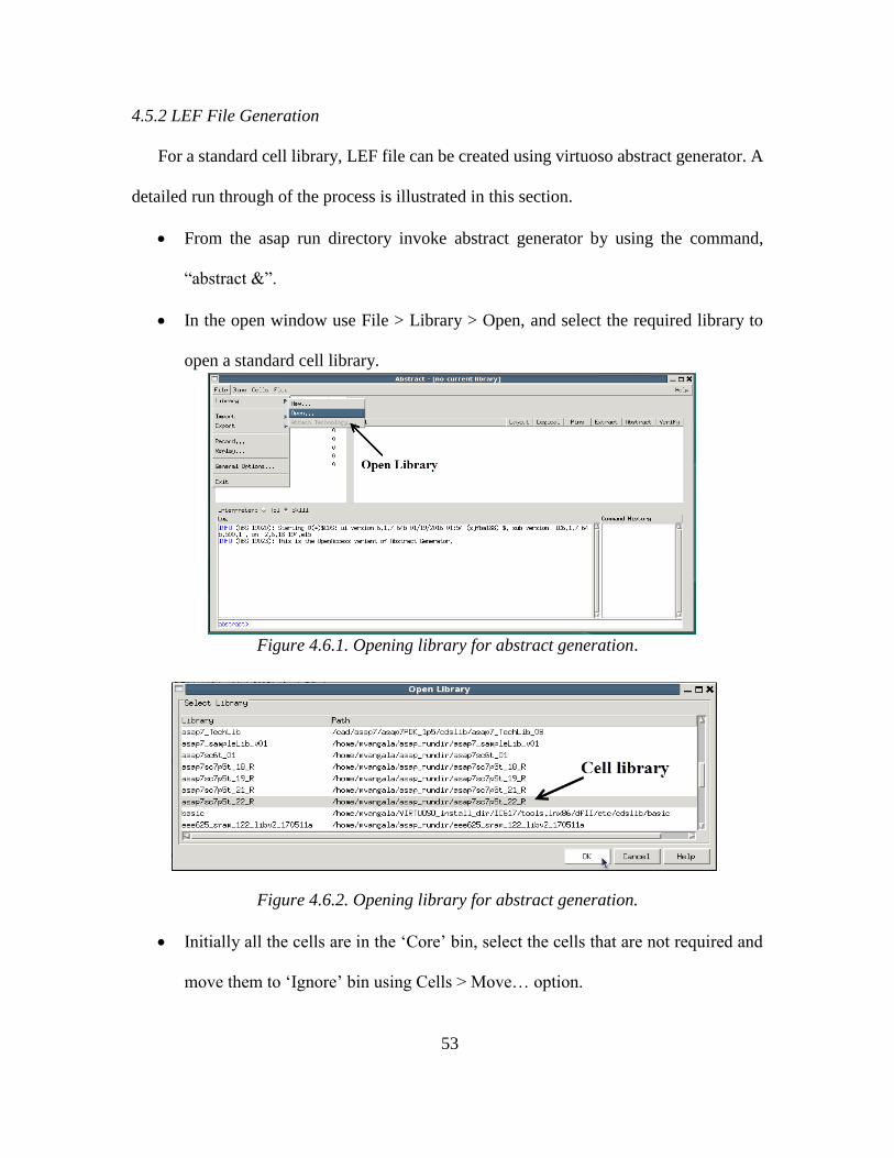
53
4.5.2 LEF File Generation
For a standard cell library, LEF file can be created using virtuoso abstract generator. A
detailed run through of the process is illustrated in this section.
• From the asap run directory invoke abstract generator by using the command,
“abstract &”.
• In the open window use File > Library > Open, and select the required library to
open a standard cell library.
Figure 4.6.1. Opening library for abstract generation.
Figure 4.6.2. Opening library for abstract generation.
• Initially all the cells are in the ‘Core’ bin, select the cells that are not required and
move them to ‘Ignore’ bin using Cells > Move… option.
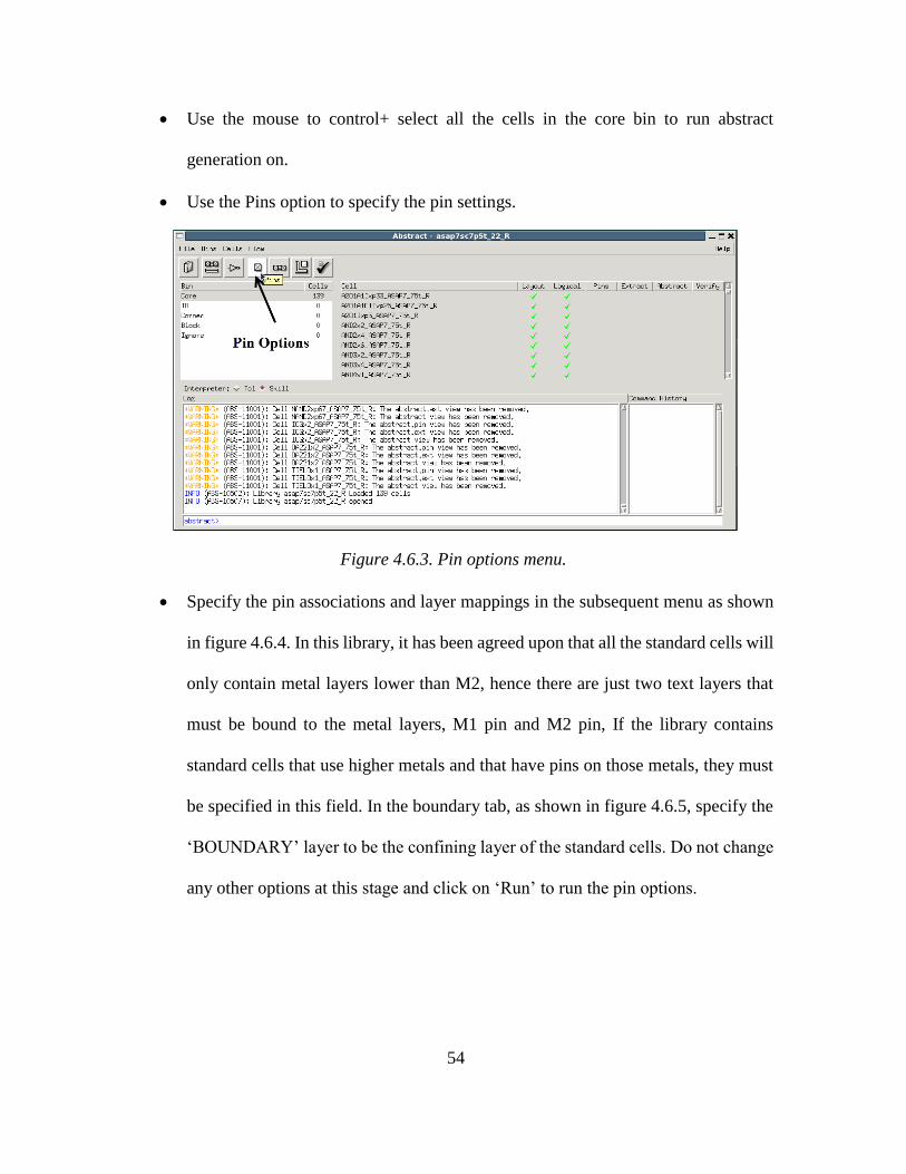
54
• Use the mouse to control+ select all the cells in the core bin to run abstract
generation on.
• Use the Pins option to specify the pin settings.
Figure 4.6.3. Pin options menu.
• Specify the pin associations and layer mappings in the subsequent menu as shown
in figure 4.6.4. In this library, it has been agreed upon that all the standard cells will
only contain metal layers lower than M2, hence there are just two text layers that
must be bound to the metal layers, M1 pin and M2 pin, If the library contains
standard cells that use higher metals and that have pins on those metals, they must
be specified in this field. In the boundary tab, as shown in figure 4.6.5, specify the
‘BOUNDARY’ layer to be the confining layer of the standard cells. Do not change
any other options at this stage and click on ‘Run’ to run the pin options.

55
Figure 4.6.4. Pins menu of abstract.
Figure 4.6.5. Boundary tab.

56
• Use the ‘Extract’ menu to set the options for pin extraction.
Figure 4.6.6. Extract Menu
• Use the ‘Signal’ and ‘Power’ tabs to set the layer assignment for extraction. Use
M1, M2, V1 and V2 layers in the menu to specify connectivity of these layers. If
the library contains cells with higher metals, include those layers and vias in this
menu.
Figure 4.6.7. Signal layer extraction.
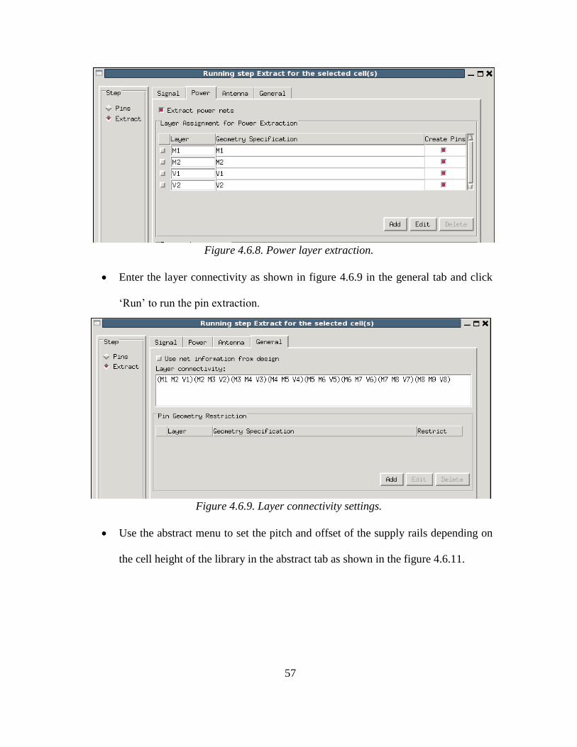
57
Figure 4.6.8. Power layer extraction.
• Enter the layer connectivity as shown in figure 4.6.9 in the general tab and click
‘Run’ to run the pin extraction.
Figure 4.6.9. Layer connectivity settings.
• Use the abstract menu to set the pitch and offset of the supply rails depending on
the cell height of the library in the abstract tab as shown in the figure 4.6.11.

58
Figure 4.6.10. Abstract settings.
Figure 4.6.11. Power rail adjustment.
• In the ‘Blockage’ tab, set the option for detailed blockage for metal M1, M2 and
via V1 and V2 and run the abstract extraction by clicking ‘Run’ option.

59
Figure 4.6.12. Blockage generation settings.
• After running the abstract step, the abstract views are added to the standard cell
library to each cell. Now using the File > Export > LEF option, the LEF file and
TechLEF file can be exported.
Figure 4.6.13. LEF export window.
• The LEF file and TechLEF file can be opened in a text editor and the macro
definitions can be read in ASCII format.
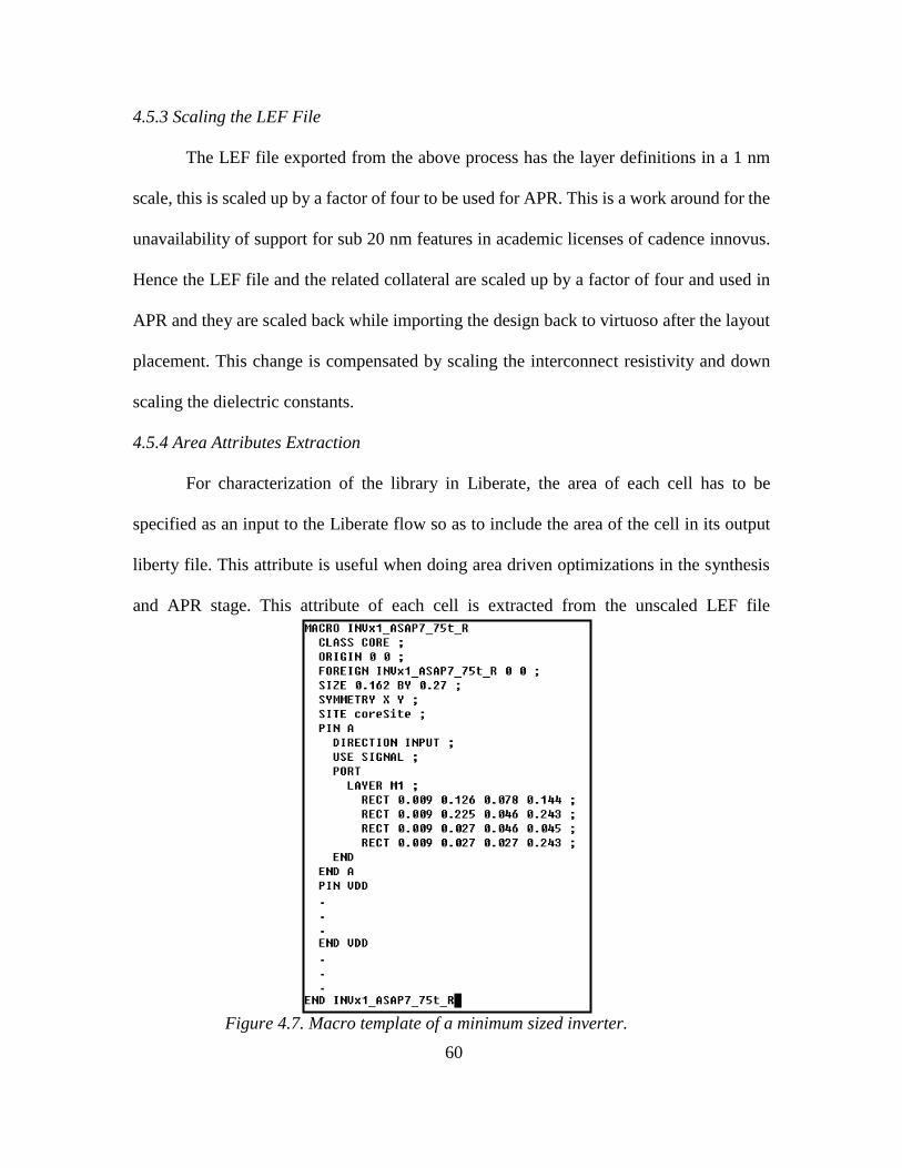
60
4.5.3 Scaling the LEF File
The LEF file exported from the above process has the layer definitions in a 1 nm
scale, this is scaled up by a factor of four to be used for APR. This is a work around for the
unavailability of support for sub 20 nm features in academic licenses of cadence innovus.
Hence the LEF file and the related collateral are scaled up by a factor of four and used in
APR and they are scaled back while importing the design back to virtuoso after the layout
placement. This change is compensated by scaling the interconnect resistivity and down
scaling the dielectric constants.
4.5.4 Area Attributes Extraction
For characterization of the library in Liberate, the area of each cell has to be
specified as an input to the Liberate flow so as to include the area of the cell in its output
liberty file. This attribute is useful when doing area driven optimizations in the synthesis
and APR stage. This attribute of each cell is extracted from the unscaled LEF file
Figure 4.7. Macro template of a minimum sized inverter.

61
containing the layout macros of the standard cells. A Perl script has been written for parsing
the macro LEF file, calculate the area of each cell and create the area_attributes.tcl file
ready to be used as an input to the Liberate characterization application. The general syntax
of a macro in the LEF file is shown in figure 4.7, here the SIZE variable gives the X and Y
coordinates of the diagonally opposite vertex to origin of the standard cell. The area of the
cell is calculated by parsing these values of X and Y and multiplying them. The resultant
area in nm2 is included in the area_attributes.tcl file.
4.5.5 LEF Vt Conversion
The LEF file obtained from this section contains the macro definitions of only the
standard cell library with RVT cells, but for the APR purpose, other Vt’s are also required
to be defined as abstract views. This can be achieved inside the LEF file by replacing the
Vt identifier in the name of the standard cell to reflect the other Vt’s. This is possible
because, the macro definitions do not have any device specific data except the name
identifier and all the standard cells of different Vt’s essentially have the same metal routing.
4.6 PEX Extraction
The CDL netlist extracted according to section 4.2 contains in it, all the device
definitions and connections between them in the cell, but it does not capture the complete
behavior of the cell because it does not contain the parasitic capacitances that a circuit has
in the physical device. This data is required for the accurate characterization of the cell.
Hence, parasitic extraction (PEX) is the process of estimating all the parasitics that a layout
may contain and creating the netlist with these capacitances added as devices. The output
netlist is called a parasitic netlist or PEX extracted netlist. In this library calibre xRC tool
is used to run parasitic extraction on the standard cells. For this thesis, a Perl script has

62
been written which used the command line calibre xRC to run the extraction on the
complete library in a single run. The pseudo code of the Perl script is shown in the figure
4.8. This script takes the name of the library as the command line input and like the DRC
and LVS runs, the .cshrc must be sourced before running this script and the path to the PEX
rule file must be updated to point to the most current file.
Figure 4.8. Pseudo code of PEX extraction Perl script.
This script creates the PEX_DIR directory with a sub directory called
Extracted_netlists which contains all parasitic netlists of all the cells in the library and can
be used directly with the Liberate characterization flow to characterize the cells. For
convenience, the options in the PEX script have been set to combine all the spice data into

63
one netlist file with the extension .pex.sp, but it can also be extracted separately into .pxi
files and .pex files by changing the ‘SINGLEFILE’ option in the pex rule file.
4.7 Liberate Characterization Flow
The main objectives of characterizing a standard cell library is to estimate the
following parameters,
➢ Logic function of the cell
➢ Delay of each cell under a series of input slew and output load conditions
➢ Power consumption of each cell under various signal conditions
➢ Leakage of each cell.
➢ Setup and hold times of the sequential cells
Hence, characterization is the process of simulating each standard cell for the above
parameters using an analog simulator and documenting them in a standardized file format
for other tools to utilize. This process takes up a big portion of library design time since
many combinations of the above data must be simulated and tabulated to create a complete
profile of the cell behavior. Therefore, an automated tool like Liberate by Cadence design
systems, Inc., is a very useful utility for the characterization of large standard cell libraries.
This tool uses an analog simulator to simulate the cell and gives the results in the standard
synopsys liberty file format. It can also generate other collateral like the Verilog
descriptions of the cells and datasheets for the cell libraries. Using Liberate, the library can
be quickly and easily characterized for all the four types of Vt values and under all the three
operating corners. The figure 4.9 gives the various files required for the Liberate run and
the output files of the run.

64
Figure 4.9. Input and output files for Liberate characterization.
4.7.1 Liberate Views and Models
Liberate essentially generates various electrical views, namely, timing views,
power views and signal integrity views, which are then tabulated into a standard synopsys
liberty file format. Each condition on the standard cell with a defined state of the inputs
and the outputs is called an arc, and Liberate writes the output liberty file organized in
terms of the arcs applied on each standard cell. For this purpose, it simulates the cell under
various input and output conditions. Out of the many things that Liberate can characterize
the cell library on, only a few (like cell delay, pin capacitance, timing constraints) are
required for obtaining a liberty file with high precision, the remaining constructs (like
steady state current, power subtraction, minimum pulse width) form a very small part of
65
the characterization flow and hence a lot of run time can be saved by avoiding calculating
them as a tradeoff for a small amount of loss in library completeness and accuracy.
This section details on the various constructs that are calculated using Liberate for
our current standard cell library. These are mainly divided into three types based on the
kind of model they are written out to in the liberty file. They are non-linear delay model
(NLDM), composite current source model (CCS) and effective current source model
(ECSM). All the constructs that Liberate can characterize can be done in one of the above
thee models and this can be controlled by issuing various different commands to the
characterization run. This model decision has to be made based on the accuracy
requirement and run time tradeoff of the characterization flow. In the Perl script written for
the characterization of the library in this thesis, a command line menu is provided to choose
between these three types of models. The various constructs that are characterized in the
current standard cell library are discussed in this section.
4.7.1.1 Delay Models
Liberate characterizes delay using NLDM, CCS and ECSM models. The NLDM
model is characterized by measuring the delay and output transition when simulating a
given range of different combinations of input transitions and output loads. In this mode,
the input transitions to this simulation are set to be ramp signals with various slew rates.
The CCS model defines transitions as a waveform instead of a single transition time, it
stores current waveforms for each point in liberty transition tables. CCS model is
characterized by attaching a voltage source to the output node before the load capacitance
and measuring the current flowing out of the output pin. This current characteristic is
tabulated in the liberty file in a current vs delay model. The ECSM model characterizes the
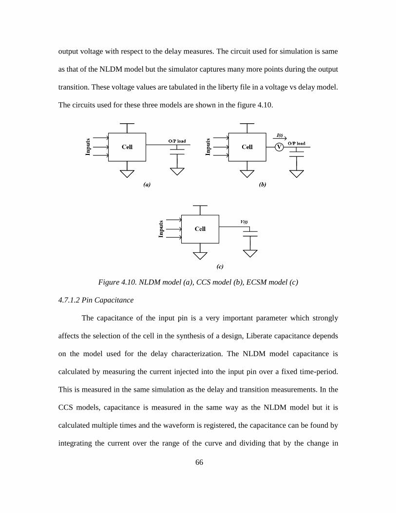
66
output voltage with respect to the delay measures. The circuit used for simulation is same
as that of the NLDM model but the simulator captures many more points during the output
transition. These voltage values are tabulated in the liberty file in a voltage vs delay model.
The circuits used for these three models are shown in the figure 4.10.
Figure 4.10. NLDM model (a), CCS model (b), ECSM model (c)
4.7.1.2 Pin Capacitance
The capacitance of the input pin is a very important parameter which strongly
affects the selection of the cell in the synthesis of a design, Liberate capacitance depends
on the model used for the delay characterization. The NLDM model capacitance is
calculated by measuring the current injected into the input pin over a fixed time-period.
This is measured in the same simulation as the delay and transition measurements. In the
CCS models, capacitance is measured in the same way as the NLDM model but it is
calculated multiple times and the waveform is registered, the capacitance can be found by
integrating the current over the range of the curve and dividing that by the change in

67
voltage. This gives a less concise but more accurate picture of the pin capacitance behavior.
For ECSM model, the pin capacitance is measured along with the ECSM delay and
transition measurements. The capacitance is measured by capturing the net current flow
into the input pin over a period of time and dividing it by the change in voltage. These
measurements are made using the hspice simulator and depending on the model used, the
simulation time varies.
4.7.1.3 Constraints
To model sequential cells accurately, alongside the delay and capacitance, the setup time
and hold time also need to be determined. These are the only type of constraints measured
in this standard cell library. Liberate recognizes the sequential cells in the library and
automatically calculates the setup and hold times for these cells. The setup and hold time
measurements involve sweeping the data pin transition with respect to the clock pin
transition and observing the output waveform. When the degradation in the output delay
waveform increases beyond a set value, it is considered the failure criteria and setup and
hold time are measured. This method is valid for flip flops whereas for latches, the setup
time is measured using the output delay degradation method and the hold time is measured
Figure 4.11. Setup time calculation (a), hold time calculation (b).

68
by observing the glitch peak in the output. The figure 4.11 illustrates these two ways of
calculating the constraints in Liberate.
4.7.1.4 Power Models
Liberate calculates three kinds of power in a circuit, the leakage power, hidden
power and active power. While calculating the leakage power, all combinations of inputs
are considered and both the channel leakage and gate leakage are calculated for a certain
combination of inputs. This power is reported in the liberty file grouped by the input
combination. Switching or active power is calculated by measuring the energy dissipated
by the cell when one or more input switches which causes one or mode outputs to change.
It includes short circuit power and the internal switching power consumed during the
charging and discharging of internal capacitive nodes. The energy contributed by the non-
switching inputs is also added to the switching power calculation. Hidden power is
calculated by measuring the energy consumed by the cell when inputs are switched but do
not cause any switching in the output. This is reported in the liberty file as the internal
power of the cell. All the power measurements are dependent on the inputs and the
switching of input states, as the number of inputs to a standard cell increase, the number of
combinations increase and the characterization time explodes.
4.7.2 Process Corners
In this standard cell library, characterization has been done at three process corners,
TT, FF and SS. Here, as the supply voltage increases the speed of the transistors increase,
hence the SS corner has a supply voltage 10% less than that of TT corner and the FF corner
has a supply voltage 10% more than that of TT corner. And it is well known that the speed
of transistor decreased as the temperature increases since the current through the channel
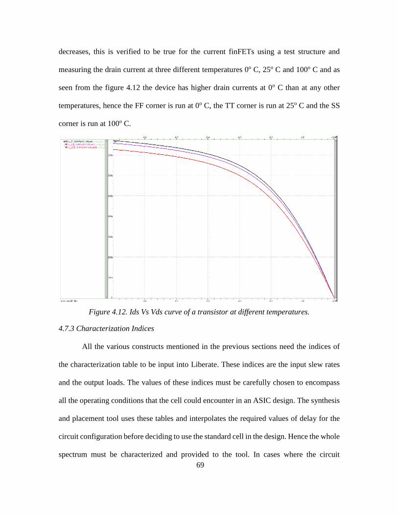
69
decreases, this is verified to be true for the current finFETs using a test structure and
measuring the drain current at three different temperatures 0o C, 25o C and 100o C and as
seen from the figure 4.12 the device has higher drain currents at 0o C than at any other
temperatures, hence the FF corner is run at 0o C, the TT corner is run at 25o C and the SS
corner is run at 100o C.
4.7.3 Characterization Indices
All the various constructs mentioned in the previous sections need the indices of
the characterization table to be input into Liberate. These indices are the input slew rates
and the output loads. The values of these indices must be carefully chosen to encompass
all the operating conditions that the cell could encounter in an ASIC design. The synthesis
and placement tool uses these tables and interpolates the required values of delay for the
circuit configuration before deciding to use the standard cell in the design. Hence the whole
spectrum must be characterized and provided to the tool. In cases where the circuit
Figure 4.12. Ids Vs Vds curve of a transistor at different temperatures.
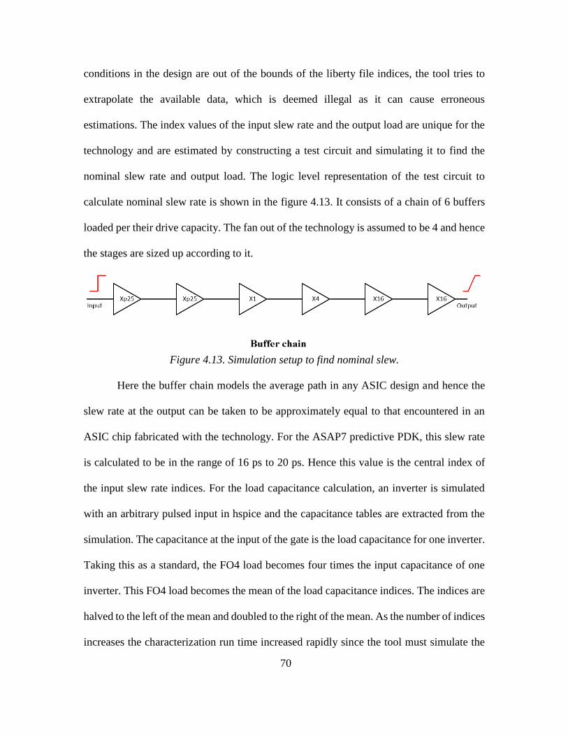
70
conditions in the design are out of the bounds of the liberty file indices, the tool tries to
extrapolate the available data, which is deemed illegal as it can cause erroneous
estimations. The index values of the input slew rate and the output load are unique for the
technology and are estimated by constructing a test circuit and simulating it to find the
nominal slew rate and output load. The logic level representation of the test circuit to
calculate nominal slew rate is shown in the figure 4.13. It consists of a chain of 6 buffers
loaded per their drive capacity. The fan out of the technology is assumed to be 4 and hence
the stages are sized up according to it.
Figure 4.13. Simulation setup to find nominal slew.
Here the buffer chain models the average path in any ASIC design and hence the
slew rate at the output can be taken to be approximately equal to that encountered in an
ASIC chip fabricated with the technology. For the ASAP7 predictive PDK, this slew rate
is calculated to be in the range of 16 ps to 20 ps. Hence this value is the central index of
the input slew rate indices. For the load capacitance calculation, an inverter is simulated
with an arbitrary pulsed input in hspice and the capacitance tables are extracted from the
simulation. The capacitance at the input of the gate is the load capacitance for one inverter.
Taking this as a standard, the FO4 load becomes four times the input capacitance of one
inverter. This FO4 load becomes the mean of the load capacitance indices. The indices are
halved to the left of the mean and doubled to the right of the mean. As the number of indices
increases the characterization run time increased rapidly since the tool must simulate the
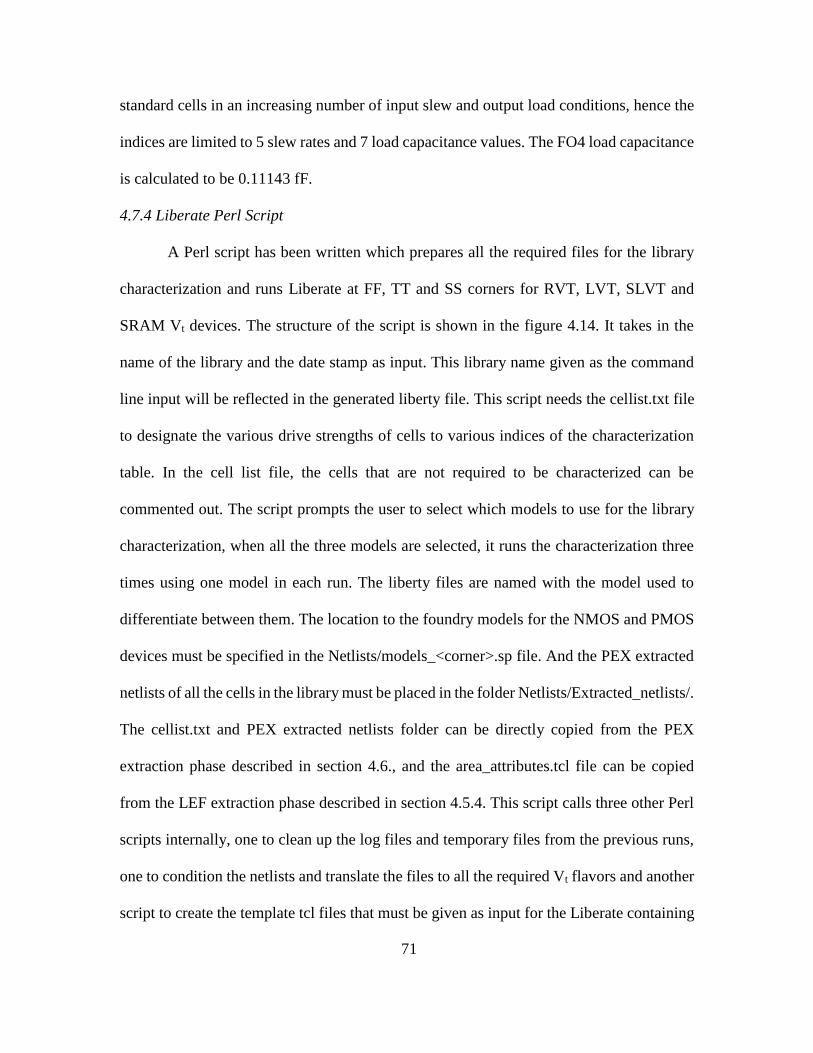
71
standard cells in an increasing number of input slew and output load conditions, hence the
indices are limited to 5 slew rates and 7 load capacitance values. The FO4 load capacitance
is calculated to be 0.11143 fF.
4.7.4 Liberate Perl Script
A Perl script has been written which prepares all the required files for the library
characterization and runs Liberate at FF, TT and SS corners for RVT, LVT, SLVT and
SRAM Vt devices. The structure of the script is shown in the figure 4.14. It takes in the
name of the library and the date stamp as input. This library name given as the command
line input will be reflected in the generated liberty file. This script needs the cellist.txt file
to designate the various drive strengths of cells to various indices of the characterization
table. In the cell list file, the cells that are not required to be characterized can be
commented out. The script prompts the user to select which models to use for the library
characterization, when all the three models are selected, it runs the characterization three
times using one model in each run. The liberty files are named with the model used to
differentiate between them. The location to the foundry models for the NMOS and PMOS
devices must be specified in the Netlists/models_<corner>.sp file. And the PEX extracted
netlists of all the cells in the library must be placed in the folder Netlists/Extracted_netlists/.
The cellist.txt and PEX extracted netlists folder can be directly copied from the PEX
extraction phase described in section 4.6., and the area_attributes.tcl file can be copied
from the LEF extraction phase described in section 4.5.4. This script calls three other Perl
scripts internally, one to clean up the log files and temporary files from the previous runs,
one to condition the netlists and translate the files to all the required Vt flavors and another
script to create the template tcl files that must be given as input for the Liberate containing

72
all the required options depending on the cells to be characterized and the models to be
used.
Figure 4.14. Structure of the library characterization script.
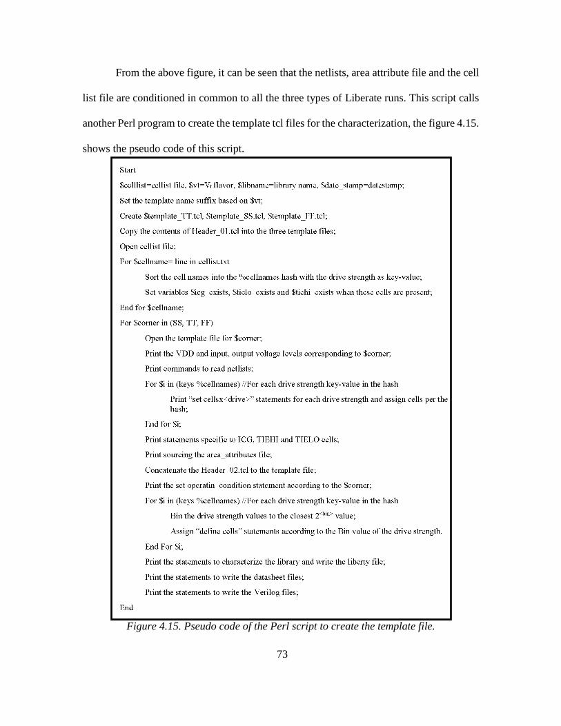
73
From the above figure, it can be seen that the netlists, area attribute file and the cell
list file are conditioned in common to all the three types of Liberate runs. This script calls
another Perl program to create the template tcl files for the characterization, the figure 4.15.
shows the pseudo code of this script.
Figure 4.15. Pseudo code of the Perl script to create the template file.
74
This script creates the template.tcl files at three corners for the given Vt value input.
These files are then used by the original Perl script to run Liberate tasks. The contents of
the template file with the various commands used for characterization are:
• Set the threshold values for slew rate measurements
• Set max transition value
• Set the directories for temporary files and simulation files
• Set the variable to control the maximum number of leakage vectors calculated.
• Set the variable to control the maximum number of hidden vectors calculated.
• Set the message limit per cell
• Create variables $inputs, $outputs, $clocks, $asyncs with the names of the input,
output, clock and asynchronous pins in the complete library.
• Set the node and value of ground and vdd.
• Set the input and output voltage levels to expect.
• Read the spice netlists for device models and cell descriptions.
• Segregate the cells based on their drive strengths into variables of the form $cellsx1,
$cellsx2, $cellsxp5 and so on.
• Define cell and pin attributed for special cells like integrated clock gaters and tie-
hi and tie-low cells.
• Source the area_attributes.tcl file to set the area variable for each cell.
• Define the delay template for all the drive strength categories. Here the drive
strengths can be approximated to the closest two’s power value. The first index of
the delay template is the input slew rate and the second index is the output pin
capacitance values.

75
• Define the power template for all the drive strengths, like the delay template, the
drive strengths can be approximated to the closest two’s power value. Here too, the
first index is the input slew rate and the second index is the output load capacitance.
• Define the constraints template to calculate the setup and hold times of the
sequential cells. Both the indices of this template are the input slew rates, the first
index is applied to the signal and the second index is applied to the clock signal.
• Set operating conditions in accordance with the corner the characterization is being
run
• Allot the various delay, power and constraint templates to the $cells variables
defined earlier. They are characterized according to the drive strength of the
template applied. The command “define_cell” is used to define these cell groups.
• Characterize the library with the required models and the available external analog
simulator
• Check the monotonicity of the delay values obtained from the characterization and
in case of discrepancies re run the characterization for that arc.
• Set the units to follow while writing out the liberty file.
• Write the liberty file of the library at the corner the characterization has been done.
• Write the Verilog descriptions of the cells.
• Write the datasheets in text and html formats.
• Save the temporary database folder as a compressed file for future usage.
This is the general flow of operations carried out by the Liberate tool for the
characterization of a library. For the purpose of this thesis, the characterization has been
done for all the cells in the library and with highest accuracy settings, hence on an average,
76
a single run of characterization which runs all the 4 Vt flavors at all three corners, i.e., 12
runs, takes about 10 to 12 hours of wall clock time. Hence a mechanism to send email
notifications when the task is completed has been written into the script file. The output
liberty file is generated in the Library folder and it contains all the 12 lib files per model
that is set to be used, i.e., 12 lib files each for the NLDM models, CCS models and ECSM
models. The datasheets and Verilog files obtained from Liberate can be directly used in the
analysis and synthesis of designs using the standard cell library.
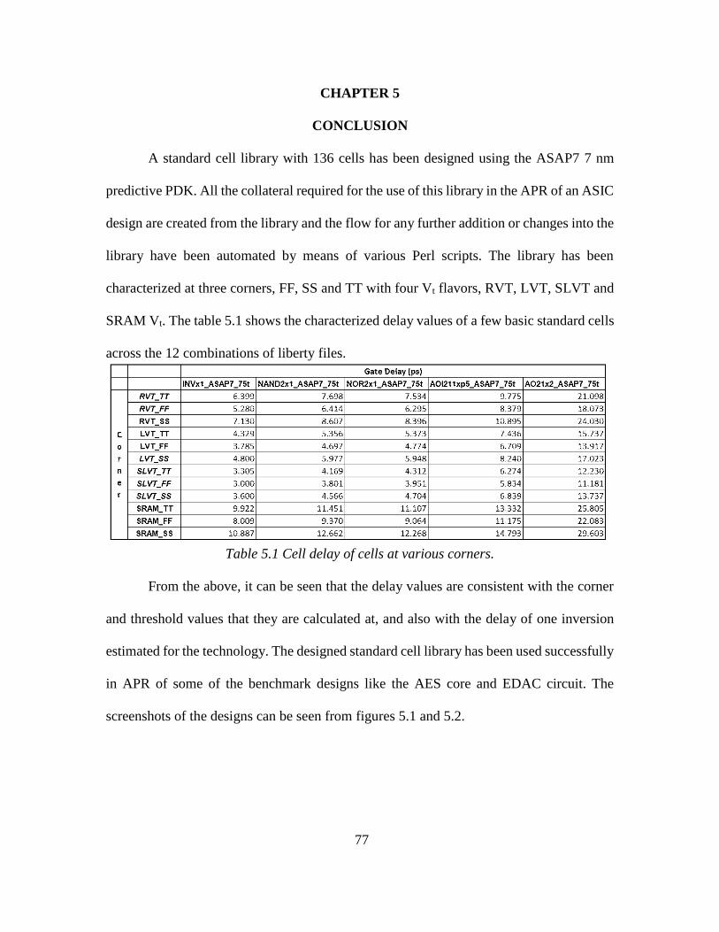
77
CHAPTER 5
CONCLUSION
A standard cell library with 136 cells has been designed using the ASAP7 7 nm
predictive PDK. All the collateral required for the use of this library in the APR of an ASIC
design are created from the library and the flow for any further addition or changes into the
library have been automated by means of various Perl scripts. The library has been
characterized at three corners, FF, SS and TT with four Vt flavors, RVT, LVT, SLVT and
SRAM Vt. The table 5.1 shows the characterized delay values of a few basic standard cells
across the 12 combinations of liberty files.
Table 5.1 Cell delay of cells at various corners.
From the above, it can be seen that the delay values are consistent with the corner
and threshold values that they are calculated at, and also with the delay of one inversion
estimated for the technology. The designed standard cell library has been used successfully
in APR of some of the benchmark designs like the AES core and EDAC circuit. The
screenshots of the designs can be seen from figures 5.1 and 5.2.
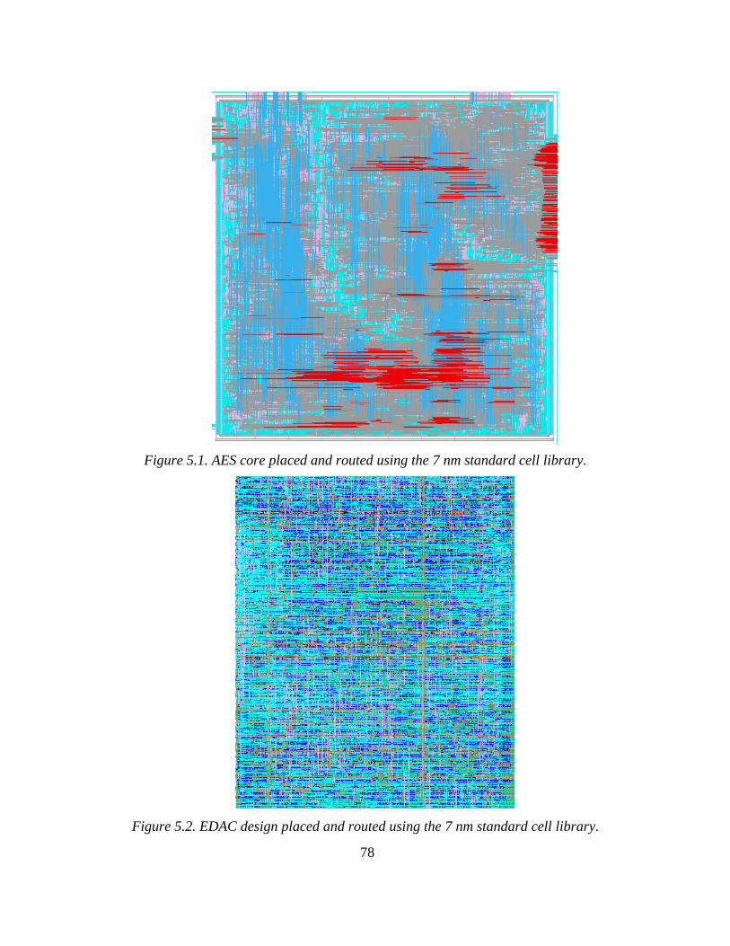
78
Figure 5.1. AES core placed and routed using the 7 nm standard cell library.
Figure 5.2. EDAC design placed and routed using the 7 nm standard cell library.

79
These APR benchmarks and experiments have been carried out iteratively using the
standard cell library fixing the various minor errors in the layouts and using the automatic
flow scripts to generate a new version of the library with the changes incorporated. The
library has been successfully used in placing and routing the control circuit in the SRAM
designed using the ASAP7 PDK outlined in [Vashish17].
Further research has been carried out using the ASAP7 PDK in the design of a 6-
track standard cell library. The resources and scripts outlined in this thesis can be used to
generate the collateral for the new library since they are based on the same PDK.

80
REFERENCES
[Abbas14] Z. Abbas, A. Mastrandrea and M. Olivieri, "A Voltage-Based Leakage Current
Calculation Scheme and its Application to Nanoscale MOSFET and FinFET Standard-Cell
Designs," in IEEE Transactions on Very Large-Scale Integration (VLSI) Systems, vol. 22,
no. 12, pp. 2549-2560, Dec. 2014.
[Abbas16] Abbas, Z., and Olivieri, M., “Optimal transistor sizing for maximum yield in
variation-aware standard cell design”, Int. J. Circ. Theory. Appl.,2016, 44: 1400–1424.
[Ameli08] B. Amelifard, S. Hatami, H. Fatemi and M. Pedram, "A Current Source Model
for CMOS Logic Cells Considering Multiple Input Switching and Stack Effect," 2008
Design, Automation and Test in Europe, Munich, 2008, pp. 568-573.
[Auth12] C. Auth, "22 nm fully-depleted tri-gate CMOS transistors," Proceedings of the
IEEE 2012 Custom Integrated Circuits Conference, San Jose, CA, 2012, pp. 1-6.
[Bhardwaj06] S. Bhardwaj, W. Wang, R. Vattikonda, Y. Cao and S. Vrudhula, "Predictive
Modeling of the NBTI Effect for Reliable Design," IEEE Custom Integrated Circuits
Conference 2006, San Jose, CA, 2006, pp. 189-192.
[Bittle10] C. Bittlestone, M. Clinton, Girishankar G., Viet le, Vinod M., Kayvan Sadra,
“15 nm Design Technology Interaction”, Texas Instruments Dallas, TX, Dec 5th 2010.
[Bohr11] Bohr M, Mistry K, “Intel’s revolutionary 22 nm transistor technology”, Intel
website, 2011.
[Cirit91] M. A. Cirit, "Characterizing a VLSI standard cell library," Proceedings of the
IEEE 1991 Custom Integrated Circuits Conference, San Diego, CA, 1991, pp. 25.7/1-
25.7/4.
[Clark16] Clark L. T., Vashishtha V., Shifren L., et al., “ASAP7: A 7 nm finFET predictive
process design kit”, Microelectronics Journal, 53,2016, pp. 105-115.
[Doyle03] B. S. Doyle et al., "High performance fully-depleted tri-gate CMOS transistors,"
in IEEE Electron Device Letters, vol. 24, no. 4, pp. 263-265, April 2003.
[Ghan15] S. Ghandali, B. Alizadeh and Z. Navabi, "Low power scheduling in high-level
synthesis using dual-Vth library," Sixteenth International Symposium on Quality
Electronic Design, Santa Clara, CA, 2015, pp. 507-511.
[Goel08] A. Goel and S. Vrudhula, "Current source based standard cell model for accurate
signal integrity and timing analysis," 2008 Design, Automation and Test in Europe,
Munich, 2008, pp. 574-579.
81
[Golan15] M. S. Golanbari, S. Kiamehr, M. B. Tahoori and S. Nassif, "Analysis and
optimization of flip-flops under process and runtime variations," Sixteenth International
Symposium on Quality Electronic Design, Santa Clara, CA, 2015, pp. 191-196.
[Gupta12] S. Gupta and S. S. Sapatnekar, "Compact Current Source Models for Timing
Analysis Under Temperature and Body Bias Variations," in IEEE Transactions on Very
Large Scale Integration (VLSI) Systems, vol. 20, no. 11, pp. 2104-2117, Nov. 2012.
[Hisam98] D. Hisamoto et al., "A folded-channel MOSFET for deep-sub-tenth micron
era," International Electron Devices Meeting 1998. Technical Digest (Cat.
No.98CH36217), San Francisco, CA, USA, 1998, pp. 1032-1034.
[IWLS05] IWLS 2005 benchmarks, http://iwls.org/iwls2005/benchmarks.html.
[James12] D. James, "Intel Ivy Bridge unveiled — The first commercial tri-gate, high-k,
metal-gateCPU," Proceedings of the IEEE 2012 Custom Integrated Circuits Conference,
San Jose, CA, 2012, pp. 1-4.
[Kaimehr15] S. Kiamehr, M. Ebrahimi, F. Firouzi and M. B. Tahoori, "Extending standard
cell library for aging mitigation," in IET Computers & Digital Techniques, vol. 9, no. 4,
pp. 206-212, 7 2015.
[Kaushik12] Kaushik Vaidyanathan et al., "Design and manufacturability tradeoffs in
unidirectional and bidirectional standard cell layouts in 14 nm node", Proc. SPIE 8327,
Design for Manufacturability through Design-Process Integration VI, March 29, 2012.
[Kuhn11] K. J. Kuhn et al., "Process Technology Variation," in IEEE Transactions on
Electron Devices, vol. 58, no. 8, pp. 2197-2208, Aug. 2011.
[Lefdef09] Cadence Design Systems, Inc., “LEF/DEF Language Reference” 2009
http://www.ispd.cc/contests/14/web/doc/lefdefref.pdf
[Lib14] Cadence.com, (2014). Cadence Virtuoso Liberate Characterization Solution.
Available at: http://www.cadence.com/products/cic/liberate/pages/default.aspx
[Lin94] Jiing-Yuan Lin, Tai-Chien Liu and Wen-Zen Shen, "A Cell-based Power
Estimation in Cmos Combinational Circuits," IEEE/ACM International Conference on
Computer-Aided Design, 1994, pp. 304-309.
[Nguy00] Nguyen Minh Duc and T. Sakurai, "Compact yet high-performance (CyHP)
library for short time-to-market with new technologies," Proceedings 2000. Design
Automation Conference. (IEEE Cat. No.00CH37106), Yokohama, Japan, 2000, pp. 475-
480.

82
[Seo08] J. s. Seo, I. L. Markov, D. Sylvester and D. Blaauw, "On the decreasing
significance of large standard cells in technology mapping," 2008 IEEE/ACM
International Conference on Computer-Aided Design, San Jose, CA, 2008, pp. 116-121.
[Sharma15] A. Sharma, Y. Sharma, S. Dasgupta and B. Anand, "Efficient static D-latch
standard cell characterization using a novel setup time model," Sixteenth International
Symposium on Quality Electronic Design, Santa Clara, CA, 2015, pp. 371-378.
[Sherazi16] Sherazi S, Chava B, Debacker P, et al., "Architectural strategies in standard-
cell design for the 7 nm and beyond technology node", J. Micro/Nanolith. MEMS MOEMS,
Feb 25, 2016, 15(1).
[Singhal06] V. Singhal and G. Girishankar, "Optimal Gate Size Selection for Standard
Cells in a Library," 2006 IEEE Dallas/CAS Workshop on Design, Applications, Integration
and Software, Richardson, TX, 2006, pp. 47-50.
[Vashish17] V. Vashishtha, M. Vangala, P. Sharma, and L. T. Clark, “Robust 7 nm SRAM
Design on a Predictive PDK,” to be presented at ISCAS, 2017.
[Woon05] Ji-Woon Yang and J. G. Fossum, "On the feasibility of nanoscale triple-gate
CMOS transistors," in IEEE Transactions on Electron Devices, vol. 52, no. 6, pp. 1159-
1164, June 2005.
[Xie15] Q. Xie, X. Lin, Y. Wang, S. Chen, M. J. Dousti and M. Pedram, "Performance
Comparisons Between 7 nm FinFET and Conventional Bulk CMOS Standard Cell
Libraries," in IEEE Transactions on Circuits and Systems II: Express Briefs, vol. 62, no.
8, pp. 761-765, Aug. 2015.
[Yang01] Yang-Kyu Choi et al., "Sub-20 nm CMOS FinFET technologies," International
Electron Devices Meeting. Technical Digest (Cat. No.01CH37224), Washington, DC,
USA, 2001, pp. 19.1.1-19.1.4.
[Yu02] Bin Yu et al., "FinFET scaling to 10 nm gate length," Digest. International Electron
Devices Meeting, San Francisco, CA, USA, 2002, pp. 251-254.

83
APPENDIX A
LIST OF CELLS IN THE STANDARD CELL LIBRARY

84
The naming convention of the cells denotes the Vt value and the drive strength of
the cells. The 75t in the cell name denotes the 7.5 track library specification.
*X=R for RVT, L for LVT, SL for SLVT and SRAM for SRAM VT
S.NO CELLNAME DESCRIPTION
1 INVxp33_ASAP7_75t_X INVERTER (x0.33 Drive)
2 INVxp67_ASAP7_75t_X INVERTER (x0.67 Drive)
3 INVx1_ASAP7_75t_X INVERTER (x1 Drive)
4 INVx2_ASAP7_75t_X INVERTER (x2 Drive)
5 INVx3_ASAP7_75t_X INVERTER (x3 Drive)
6 INVx4_ASAP7_75t_X INVERTER (x4 Drive)
7 INVx5_ASAP7_75t_X INVERTER (x5 Drive)
8 INVx6_ASAP7_75t_X INVERTER (x6 Drive)
9 INVx8_ASAP7_75t_X INVERTER (x8 Drive)
10 INVx11_ASAP7_75t_X INVERTER (x11 Drive)
11 INVx13_ASAP7_75t_X INVERTER (x13 Drive)
12 BUFx2_ASAP7_75t_X BUFFER (x2 Drive)
13 BUFx3_ASAP7_75t_X BUFFER (x3 Drive)
14 BUFx4_ASAP7_75t_X BUFFER (x4 Drive)
15 BUFX4f_ASAP7_75t_X BUFFER (x4 Drive)
16 BUFx5_ASAP7_75t_X BUFFER (x5 Drive)
17 BUFx6f_ASAP7_75t_X BUFFER (x6 Drive)
18 BUFx8_ASAP7_75t_X BUFFER (x8 Drive)
19 BUFx10_ASAP7_75t_X BUFFER (x10 Drive)
20 BUFx12f_ASAP7_75t_X BUFFER (x12 Drive)
21 BUFx12_ASAP7_75t_X BUFFER (x12 Drive)
22 BUFx16f_ASAP7_75t_X BUFFER (x16 Drive)
23 BUFx24_ASAP7_75t_X BUFFER (x24 Drive)
24 NAND2xp33_ASAP7_75t_X 2 INPUT NAND (x0.33 Drive)
25 NAND2xp5_ASAP7_75t_X 2 INPUT NAND (x0.5 Drive)
26 NAND2xp67_ASAP7_75t_X 2 INPUT NAND (x0.67 Drive)
27 NAND2x1_ASAP7_75t_X 2 INPUT NAND (x1 Drive)
28 NAND2x1p5_ASAP7_75t_X 2 INPUT NAND (x1.5 Drive)
29 NAND3x1_ASAP7_75t_X 3 INPUT NAND (x1 Drive)
30 NAND4xp25_ASAP7_75t_X 4 INPUT NAND (x0.25 Drive)
31 NAND5xp2_ASAP7_75t_X 5 INPUT NAND (x0.2 Drive)
32 AND2x2_ASAP7_75t_X 2 INPUT AND (x2 Drive)

85
33 AND2x4_ASAP7_75t_X 2 INPUT AND (x4 Drive)
34 AND2x6_ASAP7_75t_X 2 INPUT AND (x6 Drive)
35 AND3x2_ASAP7_75t_X 3 INPUT AND (x2 Drive)
36 AND3x4_ASAP7_75t_X 3 INPUT AND (x4 Drive)
37 AND4x1_ASAP7_75t_X 4 INPUT AND (x1 Drive)
38 AND4x2_ASAP7_75t_X 4 INPUT AND (x2 Drive)
39 AND5x2_ASAP7_75t_X 5 INPUT AND (x2 Drive)
40 NOR2xp33_ASAP7_75t_X 2 INPUT NOR (x0.33 Drive)
41 NOR2x67_ASAP7_75t_X 2 INPUT NOR (x0.67 Drive)
42 NOR2x1_ASAP7_75t_X 2 INPUT NOR (x1 Drive)
43 NOR3x1_ASAP7_75t_X 3 INPUT NOR (x1 Drive)
44 NOR4xp25_ASAP7_75t_X 4 INPUT NOR (x0.25 Drive)
45 NOR5xp2_ASAP7_75t_X 5 INPUT NOR (x0.2 Drive)
46 OR2x2_ASAP7_75t_X 2 INPUT OR (x2 Drive)
47 OR2x4_ASAP7_75t_X 2 INPUT OR (x4 Drive)
48 OR2x6_ASAP7_75t_X 2 INPUT OR (x6 Drive)
49 OR3x2_ASAP7_75t_X 3 INPUT OR (x2 Drive)
50 OR3x4_ASAP7_75t_X 3 INPUT OR (x4 Drive)
51 OR4x1_ASAP7_75t_X 4 INPUT OR (x1 Drive)
52 OR4x2_ASAP7_75t_X 4 INPUT OR (x2 Drive)
53 AOI21xp5_ASAP7_75t_X 2-1 AOI (x0.5 Drive)
54 AOI22xp33_ASAP7_75t_X 2-2 AOI (x0.33 Drive)
55 AOI31xp67_ASAP7_75t_X 3-1 AOI (x0.67 Drive)
56 AOI32xp33_ASAP7_75t_X 3-2 AOI (x0.33 Drive)
57 AOI33xp33_ASAP7_75t_X 3-3 AOI (x0.33 Drive)
58 AOI211xp5_ASAP7_75t_X 2-1-1 AOI (x0.5 Drive)
59 AOI221xp5_ASAP7_75t_X 2-2-1 AOI (x0.5 Drive)
60 AOI332xp67_ASAP7_75t_X 3-3-2 AOI (x0.67 Drive)
61 AOI333xp67_ASAP7_75t_X 3-3-3 AOI (x0.67 Drive)
62 OAI21xp5_ASAP7_75t_X 2-1 OAI (x0.5 Drive)
63 OAI22xp5_ASAP7_75t_X 2-2 OAI (x0.5 Drive)
64 OAI31xp67_ASAP7_75t_X 3-1 OAI (x0.67 Drive)
65 OAI32xp33_ASAP7_75t_X 3-2 OAI (x0.33 Drive)
66 OAI33xp33_ASAP7_75t_X 3-3 OAI (x0.33 Drive)
67 AO21x2_ASAP7_75t_X 2-1 AO (x2 Drive)
68 AO22x2_ASAP7_75t_X 2-2 AO (x2 Drive)
69 AO31x2_ASAP7_75t_X 3-1 AO (x2 Drive)
70 AO32x2_ASAP7_75t_X 3-2 AO (x2 Drive)
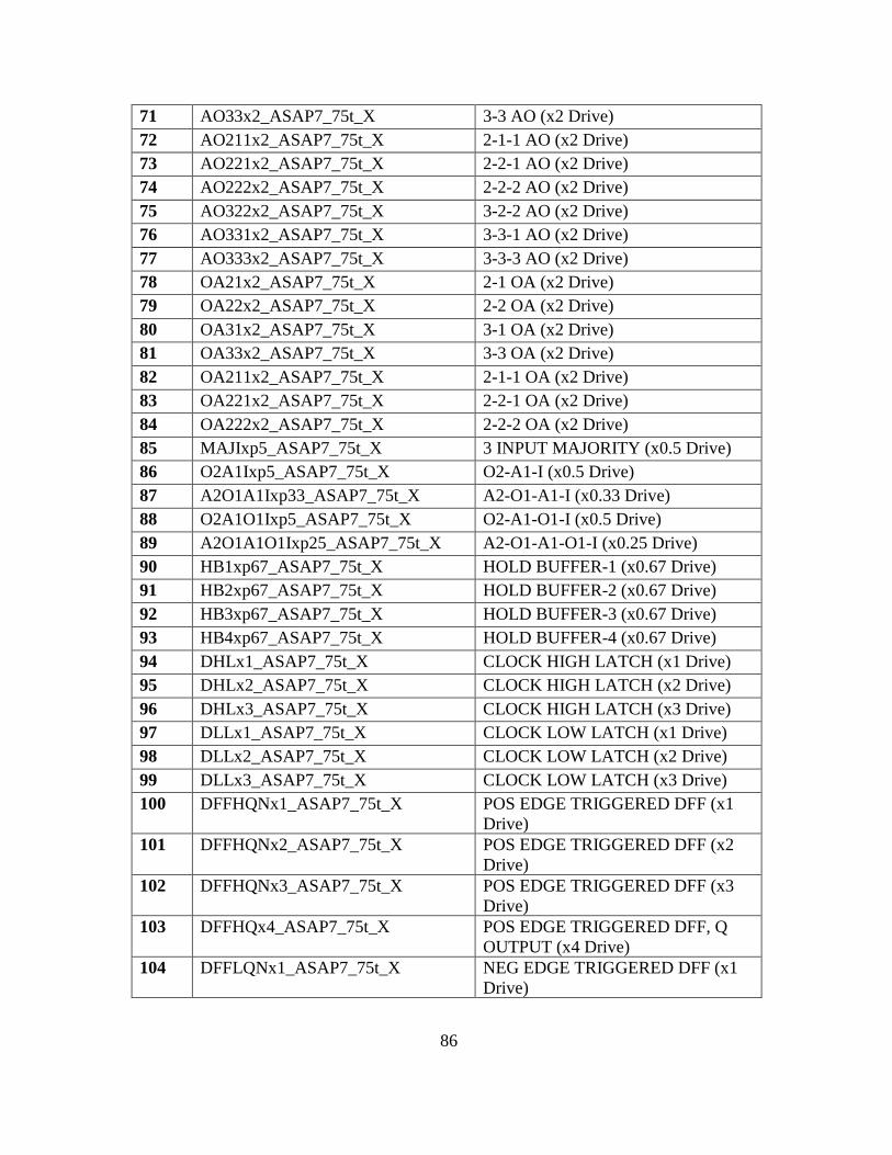
86
71 AO33x2_ASAP7_75t_X 3-3 AO (x2 Drive)
72 AO211x2_ASAP7_75t_X 2-1-1 AO (x2 Drive)
73 AO221x2_ASAP7_75t_X 2-2-1 AO (x2 Drive)
74 AO222x2_ASAP7_75t_X 2-2-2 AO (x2 Drive)
75 AO322x2_ASAP7_75t_X 3-2-2 AO (x2 Drive)
76 AO331x2_ASAP7_75t_X 3-3-1 AO (x2 Drive)
77 AO333x2_ASAP7_75t_X 3-3-3 AO (x2 Drive)
78 OA21x2_ASAP7_75t_X 2-1 OA (x2 Drive)
79 OA22x2_ASAP7_75t_X 2-2 OA (x2 Drive)
80 OA31x2_ASAP7_75t_X 3-1 OA (x2 Drive)
81 OA33x2_ASAP7_75t_X 3-3 OA (x2 Drive)
82 OA211x2_ASAP7_75t_X 2-1-1 OA (x2 Drive)
83 OA221x2_ASAP7_75t_X 2-2-1 OA (x2 Drive)
84 OA222x2_ASAP7_75t_X 2-2-2 OA (x2 Drive)
85 MAJIxp5_ASAP7_75t_X 3 INPUT MAJORITY (x0.5 Drive)
86 O2A1Ixp5_ASAP7_75t_X O2-A1-I (x0.5 Drive)
87 A2O1A1Ixp33_ASAP7_75t_X A2-O1-A1-I (x0.33 Drive)
88 O2A1O1Ixp5_ASAP7_75t_X O2-A1-O1-I (x0.5 Drive)
89 A2O1A1O1Ixp25_ASAP7_75t_X A2-O1-A1-O1-I (x0.25 Drive)
90 HB1xp67_ASAP7_75t_X HOLD BUFFER-1 (x0.67 Drive)
91 HB2xp67_ASAP7_75t_X HOLD BUFFER-2 (x0.67 Drive)
92 HB3xp67_ASAP7_75t_X HOLD BUFFER-3 (x0.67 Drive)
93 HB4xp67_ASAP7_75t_X HOLD BUFFER-4 (x0.67 Drive)
94 DHLx1_ASAP7_75t_X CLOCK HIGH LATCH (x1 Drive)
95 DHLx2_ASAP7_75t_X CLOCK HIGH LATCH (x2 Drive)
96 DHLx3_ASAP7_75t_X CLOCK HIGH LATCH (x3 Drive)
97 DLLx1_ASAP7_75t_X CLOCK LOW LATCH (x1 Drive)
98 DLLx2_ASAP7_75t_X CLOCK LOW LATCH (x2 Drive)
99 DLLx3_ASAP7_75t_X CLOCK LOW LATCH (x3 Drive)
100 DFFHQNx1_ASAP7_75t_X POS EDGE TRIGGERED DFF (x1
Drive)
101 DFFHQNx2_ASAP7_75t_X POS EDGE TRIGGERED DFF (x2
Drive)
102 DFFHQNx3_ASAP7_75t_X POS EDGE TRIGGERED DFF (x3
Drive)
103 DFFHQx4_ASAP7_75t_X POS EDGE TRIGGERED DFF, Q
OUTPUT (x4 Drive)
104 DFFLQNx1_ASAP7_75t_X NEG EDGE TRIGGERED DFF (x1
Drive)

87
105 DFFLQNx2_ASAP7_75t_X NEG EDGE TRIGGERED DFF (x2
Drive)
106 DFFLQNx3_ASAP7_75t_X NEG EDGE TRIGGERED DFF (x3
Drive)
107 DFFLQx4_ASAP7_75t_X NEG EDGE TRIGGERED DFF, Q
OUTPUT (x4 Drive)
108 ASYNC_DFFHx1_ASAP7_75t_X ASYNCHRONOUS SET-RESET FF
(x1 Drive)
109 SDFHx1_ASAP7_75t_X POS EDGE TRIGGERED SCAN FF
(x1 Drive)
110 SDFHx2_ASAP7_75t_X POS EDGE TRIGGERED SCAN FF
(x2 Drive)
111 SDFHx3_ASAP7_75t_X POS EDGE TRIGGERED SCAN FF
(x3 Drive)
112 SDFHx4_ASAP7_75t_X POS EDGE TRIGGERED SCAN FF
(x4 Drive)
113 SDFLx1_ASAP7_75t_X NEG EDGE TRIGGERED SCAN FF
(x1 Drive)
114 SDFLx2_ASAP7_75t_X NEG EDGE TRIGGERED SCAN FF
(x2 Drive)
115 SDFLx3_ASAP7_75t_X NEG EDGE TRIGGERED SCAN FF
(x3 Drive)
116 SDFLx4_ASAP7_75t_X NEG EDGE TRIGGERED SCAN FF
(x4 Drive)
117 FAx1_ASAP7_75t_X 1- BIT FULL ADDER (x1 Drive)
118 HAxp5_ASAP7_75t_X 1- BIT HALF ADDER (x1 Drive)
119 XOR2xp5_ASAP7_75t_X 2 INPUT XOR (x0.5 Drive)
120 XOR2x1_ASAP7_75t_X 2 INPUT XOR (x1 Drive)
121 XNOR2xp5_ASAP7_75t_X 2 INPUT XNOR (x0.5 Drive)
122 XNOR2x1_ASAP7_75t_X 2 INPUT XNOR (x1 Drive)
123 ICGx1_ASAP7_75t_X INTEGRATED CLOCK GATER (x1
Drive)
124 ICGx2_ASAP7_75t_X INTEGRATED CLOCK GATER (x2
Drive)
125 ICGx3_ASAP7_75t_X INTEGRATED CLOCK GATER (x3
Drive)
126 TIELOx1_ASAP7_75t_X TIE LOW CELL (x1 Drive)
127 TIEHIx1_ASAP7_75t_X TIE HIGH CELL (x1 Drive)
128 TAPCELL_ASAP7_75t_X TAP CELL
129 TAPCELL_WITH_FILLER_ASAP7
_75t_X
TAPCELL WITH FILLER
130 FILLER_ASAP7_75t_X FILLER CELL
131 FILLERxp5_ASAP7_75t_X FILLER CELL

88
132 DECAPx1_ASAP7_75t_X DECAP (x1 Drive)
133 DECAPx2_ASAP7_75t_X DECAP (x2 Drive)
134 DECAPx4_ASAP7_75t_X DECAP (x4 Drive)
135 DECAPx6_ASAP7_75t_X DECAP (x6 Drive)
136 DECAPx10_ASAP7_75t_X DECAP (x10 Drive)