first principles study of complex crystalline solidskasinath/mastersthesis_kasinathan.pdf · this...
TRANSCRIPT
Final Project Report on
First Principles Study Of ComplexCrystalline Solids
Submitted in partial fulfillment of the requirementsfor the degree ofMaster of Science
By
Deepa KasinathanRoll No. 99512006
under the guidance of
Prof. Indra Das GuptaDepartment of Physics
INDIAN INSTITUTE OF TECHNOLOGYBOMBAYApril 2001

Certificate
This is to certify that the work presented in this report has been done under mysupervision.
Prof. Indra Das Gupta
2

Acceptance Certificate
June 14, 2001
This is to certify that the project report entitled “First Principles Studyof Complex Crystalline Solids” by Deepa Kasinathan (99512006) isapproved for the Degree of Master of Science in Physics.
Guide Chairperson Examiner
3

Acknowledgement
June 14, 2001
I would like to be thankful to my guide Prof. Indra Das Gupta for guid-ing me throughout the project programme and giving me invaluable suggestionswithout which this work could not have been completed.
Deepa Kasinathan
i

Contents
1 Introduction and Motivation 1
2 First principles electronic structure calculations 4
2.1 Outline of the problem . . . . . . . . . . . . . . . . . . . . . . . . 4
2.2 Origin of the solution . . . . . . . . . . . . . . . . . . . . . . . . . 4
2.3 Density Functional Theory . . . . . . . . . . . . . . . . . . . . . . 5
2.3.1 Hartree Approximation and Self Consistency . . . . . . . . 6
2.4 One-particle Kohn-Sham equation . . . . . . . . . . . . . . . . . . 7
2.5 Basic Formalism of LMTO method . . . . . . . . . . . . . . . . . 9
2.5.1 The Method of Linearized Mu!n Tin Orbitals . . . . . . . 10
2.5.2 Mu!n-Tin Orbitals (MTO) and their representation . . . 11
2.6 The Hamiltonian and The Overlap Matrices . . . . . . . . . . . . 14
2.7 Derivation of the COHP . . . . . . . . . . . . . . . . . . . . . . . 16
ii

3 Case Study - Silicon and Nickel Silicide 19
3.1 Silicon . . . . . . . . . . . . . . . . . . . . . . . . . . . . . . . . . 19
3.1.1 Structure . . . . . . . . . . . . . . . . . . . . . . . . . . . 19
3.1.2 Details of the LDA LMTO-ASA calculations . . . . . . . . 20
3.2 Nickel Silicide . . . . . . . . . . . . . . . . . . . . . . . . . . . . . 26
3.2.1 Details of LDA LMTO-ASA calculations . . . . . . . . . . 27
4 Electronic Structure and Thermoelectric Properties of Narrow-gap Materials FeVSb and FeNbSb 31
4.1 Crystal Structure in real and reciprocal space . . . . . . . . . . . 32
4.2 Results . . . . . . . . . . . . . . . . . . . . . . . . . . . . . . . . . 34
4.3 XSb (X = Nb, V) - Model System for comparison . . . . . . . . . 35
4.4 FeNbSb / FeVSb . . . . . . . . . . . . . . . . . . . . . . . . . . . 38
4.5 Origin of the gap formation . . . . . . . . . . . . . . . . . . . . . 39
4.6 COHP . . . . . . . . . . . . . . . . . . . . . . . . . . . . . . . . . 39
4.7 Calculation of Seebeck Co-e!cient . . . . . . . . . . . . . . . . . 43
5 Study of Chevrel phases for possible thermoelectric applications 47
5.1 Structure of Mo6X8 . . . . . . . . . . . . . . . . . . . . . . . . . . 48
iii

5.2 Details of LDA LMTO-ASA calculations . . . . . . . . . . . . . . 51
5.2.1 Band Structure . . . . . . . . . . . . . . . . . . . . . . . . 51
5.2.2 Density of States . . . . . . . . . . . . . . . . . . . . . . . 51
5.3 SnMo6Se8 . . . . . . . . . . . . . . . . . . . . . . . . . . . . . . . 53
5.3.1 Band Structure . . . . . . . . . . . . . . . . . . . . . . . . 53
5.3.2 Density of states . . . . . . . . . . . . . . . . . . . . . . . 54
5.4 E"ect of insertion of small cations . . . . . . . . . . . . . . . . . . 55
5.4.1 Density of States . . . . . . . . . . . . . . . . . . . . . . . 55
5.4.2 Band Structure . . . . . . . . . . . . . . . . . . . . . . . . 56
6 Outlook 57
iv

List of Figures
2.1 The Mu!n-Tin approximation . . . . . . . . . . . . . . . . . . . . 11
3.1 The Diamond Cubic Crystal Structure of Silicon. . . . . . . . . . 20
3.2 Reciprocal Lattice, high symmetry points and Brillouin zone . . . 21
3.3 The Band Structure of Silicon. . . . . . . . . . . . . . . . . . . . . 22
3.4 Density Of States Of Silicon. . . . . . . . . . . . . . . . . . . . . . 23
3.5 COHP and Integrated COHP of Si-Si bond . . . . . . . . . . . . . 24
3.6 Fluorite structure of NiSi2 . . . . . . . . . . . . . . . . . . . . . . 26
3.7 The Band Structure of NiSi2. . . . . . . . . . . . . . . . . . . . . 28
3.8 Density of states of NiSi2 . . . . . . . . . . . . . . . . . . . . . . . 29
3.9 COHP and Integrated COHP of NiSi2 . . . . . . . . . . . . . . . 30
4.1 The Structure of a half-heusler compound. . . . . . . . . . . . . . 32
4.2 The Crystal Structure of FeXSb (X = V, Nb.) . . . . . . . . . . . 33
v

4.3 The Brillouin zone for a half-Heusler compound. . . . . . . . . . . 33
4.4 Minimisation of Energy with respect to lattice constant. . . . . . 34
4.5 Total band structure and total DOS of NbSb and VSb. . . . . . . 35
4.6 Partial band structure of Sb-s and Nb-s orbitals in NbSb and VSb. 36
4.7 Fat band structure of Sb-p and X-eg in NbSb and VSb. . . . . . . 37
4.8 Fat band structure of Nb/V-t2g and Fe-d orbitals in FeNbSb/FeVSb. 38
4.9 COHP and Integrated COHP for FeNbSb . . . . . . . . . . . . . . 41
4.10 COHP and Integrated COHP for FeVSb . . . . . . . . . . . . . . 42
4.11 Seebeck Co-e!cient for FeNbSb. . . . . . . . . . . . . . . . . . . . 45
4.12 Seebeck Co-e!cient for FeVSb. . . . . . . . . . . . . . . . . . . . 46
5.1 Building block arrangement. . . . . . . . . . . . . . . . . . . . . . 49
5.2 Elementary cell of rhombohedral structure . . . . . . . . . . . . . 49
5.3 Projection on the hexagonal(1120) plane. . . . . . . . . . . . . . . 50
5.4 Distribution of small cations in the lattice . . . . . . . . . . . . . 51
5.5 Band structure of Mo6Se8 . . . . . . . . . . . . . . . . . . . . . . 52
5.6 Density of states of Mo6Se8. . . . . . . . . . . . . . . . . . . . . . 52
5.7 Band structure of SnMo6Se8 . . . . . . . . . . . . . . . . . . . . . 53
vi

5.8 Density of states of SnMo6Se8 . . . . . . . . . . . . . . . . . . . . 54
5.9 Density of States of Cu2Mo6Se8 . . . . . . . . . . . . . . . . . . . 55
5.10 Band structure of Cu2Mo6Se8 . . . . . . . . . . . . . . . . . . . . 56
vii

Chapter 1
Introduction and Motivation
Tailoring materials with desirable set of properties for intended applicationis one of the important aspects of the present day materials research. Atom-istic simulations of physical properties from first principles have become maturedwith the advent of powerful computers and can be exploited for predicting thebehaviour of materials without actually synthesizing them thereby providing auseful guide in our seach for better materials, stronger materials, materials whichcorrode less, better magnets, better superconductors, and so on. The recentadvances in the first principles calculations of the material properties may beattributed to the following developments (a) The Hohenberg-Kohn-Sham den-sity functional theory which rigoursly proved, that the complicated and unman-ageable many body problem can be transformed into an e"ective one-electronproblem, which in turn could be solved within the so called local density ap-proximation, (b) The linearized band structure methods introduced by Andersonfor solving the electronic structure of solids. The linearized augumented planewave (LAPW) method and the linearised mu!n tin orbital (LMTO) method,the linearized version of the augumented plane wave (APW) and the Korringa-Kohn-Rostoker (KKR) method respectively, are most widely used today for firstprinciples (ab initio) investgation of materials. The full potential version of bothLMTO and LAPW which makes no shape approximation of the potential andcharge density is now capable of providing cohesive properties of materials withmetalurgical accuracy. In the present project we propose to study the chemicalbonding and the cohesive properties of thermoelectric materials which attractedconsiderable interest in the recent times.
In the recent years there is a growing research activity in the search for newand better thermoelectric materials. The reason for the growing interest may be

2
attributed to several factors. There is an increasing environmental concern aboutchloroflurocarbons used in most compressor based refrigeration technologies andcould be avoided if an e!cient Peltier refrigirator could be devloped. In additionthe generation of electric power from the waste heat using thermoelctrics is anattractive option for several applications, including the conversion of automobileexhaust and engine heat into useful power. The e!ciency of a thermoelectricmaterial is characterized by a dimensionless figure of merit
ZT = !S2TK = S2
L ,
where T is the temperature, ! is the electrical conductivity, S is the seebeck co-e!cient (thermopower) and K is the thermal conductivity which contains bothelectronic and lattice contributions, K = Kelec + Klat. The ratio L= K
!T , whichis often called the Lorentz number is ordinarily limited from below by its elec-
tronic value, Kel!T , given by the Widemann Franz value L="2
3 (kBe )2. On these
grounds, the metals are poor thermoelectric materials because of low Seebeckcoe!cient and a large contribution to the thermal conductivity. Insulators (orlightly doped semiconductors) have a large contribution to the thermal conduc-tivity, but have too few carriers, which results in a large electrical resistivity. Solargest value of ZT is obtained midway between two extremes metal or insulatorand for the optimum thermoelectric performance the energy gap of the semicon-ductor must be atleast ten times kTmax where Tmax is the maximum operatingtemperature, otherwise the simultaneous excitations of intrinsic electrons andholes lowers S and ZT. Though the carrier concentration plays a crucial role tochange electrical and thermal properties of thermoelectric materials but the abil-ity of the lattice to conduct heat is only slightly a"ected by the changes in carrierconcentration. Hence if the lattice thermal conductivity is high ZT will be low.According to Slack9 an ideal thermoelectric material with high figure of meritshould be a phonon glass and an electron crystal which conducts heat like a glassand electricity like a metal. So search for good thermoelectric materials shouldnot only be confined to narrow gap semiconductors but also to materials whichhave minimum lattice thermal conductivity. Empirical evidence suggests that alow thermal conductivity is found in materials with the following four character-istics, (a) large number of atoms in the unit cell, (b) large average atomic mass,(c) crystal structure that result in a high verage co-ordination number per atomand (d) cage like structures in which a weakly bound atom or molecule in thecage rattles i.e has a large thermal parameter.
At this point the first principles electronic structure calculations are prov-ing to be a useful tool in sorting out mechanism by which high ZT values can arise

3
in the complex materials and in explaining the various chemical modifications onthe thermoelectric properties. Recent study by S.D. Mahanti et al.13 about theelectronic structure of a class of half-Heusler compounds MNiPn, where M is Y,La, Lu, Yb, and Pn is a pnicogen As, Sb, Bi, showed that all these systems except-ing Yb are narrow-gap semiconductors and were found to be potential candidatesfor high-performance thermoelectric materials. Similarly, the work by R.J. Cavaet al.14 on pure and doped half-Heusler compounds FeVSb and FeNbSb showedthat these systems are also narrow band gap semiconductors. The other goodcandidates are the Chevrel phases. Though Chevrel phases recieved immenseattention in the early eighties for their superconducting properties but the semi-conducting compositions as a potential candidate for thermoelectric materail onlyattracted recent attention. Chevrel phases are family of Mo cluster compoundsand are based on binary Mo6X8, where X is a chalcogen (S,Se,Te). The crystalstructure consists of large voids which may be filled with metals having generalformula MxMo6X8. This o"ers an oppurtunity to obtain low thermal conductivityas well as a chemical knob to modify the electronic properties.
Though in the recent years several electronic structure calculations havebeen performed in these materials, still lot remains to be done. In particular thephysical origin of the gap formation in these materials is a crucial and subtleissue which has not been investigated systematically. Investigation need to bedone other than chemistry what are the factors which could influence the gapand therefore the thermoelectric properties of these materials. The influence ofpressure on the chemical bonding and the gap formation remains to be explored.The goal of the present project is to address some of these questions.
The remainder of this report is organised as follows: In chapter 2, we shallreview the first principles electronic structure calculations using the Density func-tional theory and the Tight Binding Linearised Mu!n-Tin Orbital (TB-LMTO)method. In particular we shall discuss the indicators of chemical bonding withinTB-LMTO. In chapter 3, we shall apply our methodology to analyse simple el-ement, Silicon and then Nickel Silicide (NiSi2). In chapter 4, we consider thehalf-Heusler compounds FeVSb and FeNbSb which has been suggested as a pos-sible candidate for thermoelectric applicationsand analyse its band structure. Inchapter 5, we shall consider the electronic structure of Chevrel phases and alsosee the e"ect of insertion of cations in it. Finally we present the results andconclusions that we obtained.

Chapter 2
First principles electronicstructure calculations
2.1 Outline of the problem
We wish to address the question, what are the energies and the wave functionsof electrons in a solid under the influnce of the nuclei as well as other electrons.The fundamental problem in this regard is the solution of Schrodingers equationfor many electron systems with interaction among the electrons and the nuclei.One of the approaches to the solution of this problem, which is the basis of themodern quantitative theory for electronic structure calculations is to rigourouslymap the problem of many electrons onto the problem of an independent electronmoving in the mean field of the other electrons and ions.
2.2 Origin of the solution
The solution to the above problem started o" with the Born-Oppenheimer
approximation. This approximation amounts to saying that we can seperate theelectronic and nuclear degrees of freedom. Because the electronic mass is so muchsmaller than that of the nuclei the electrons respond almost instantaneously tothe changes in the positions of the nuclei. It is a good approximation to say thatthe electrons are always in their ground state as the atoms of the solid vibratethermally. This means that the positions of the nuclei are parameters that appearin the potential of the schrodinger equation defining the wave functions of theelectrons.

5
2.3 Density Functional Theory
The next advent for the independent electron approximation came with thedevelopment of density functional theory (DFT) by Hohenberg-Kohn-Sham1,2.The basic idea of DFT originated from the query ‘can we arrive at a poten-tial V(r) uniquely, given the charge density "(r) of the system?’. The densityfunctional theory yields two results, one important conceptually and the other aframework for practical calculations:
• The solution of the many-body ground state problem is reduced exactly tothe solution for the ground-state density distribution "(r) given by one-particleschrodinger equation. The e"ective potential in the schrodinger equationincludes, in principle all the interaction e"ects: the Hartree potential (thecoulomb potential due to the charge distribution when the electrons aretreated as fixed), the exchange potential (due to the interaction describedby the Pauli exclusion principle), and the correlation potential (due to thee"ect of the given electron on the overall charge distribution).
• An approximation for e"ective potential is given by regarding a small neigh-bourhood of the electron system. This result forms the so-called ‘local-density-functional’ approximation.
Thus the charge density becomes the central quantity that must be found, inthe place of many electron wave functions. More formally Hohenberg and Kohnshowed that the ground state energy is a unique functional of "(r). Unfortunatelythe functional is not known! But whatever the functional is, it acquires a min-imum value when the charge density is the correct ground state charge density.Mathematically this means that we have to use a variational principle for findingthe charge density.
Then, Kohn and Sham derived a system of one-particle equations for thedescription of the electronic ground state. The interacting N-electron problemwas thus mapped exactly onto N single particle equations. This means eachelectron is moving independently of the other electrons, but it experiences ane"ective potential which emulates all the interactions with the other electrons.This gives the rigorous justification for the independent electron approximationwhich we will be using all along. It was also showed that the e"ective potential isa unique functional of the charge density. The one-particle equations are known

6
as the Kohn-Sham equations.
2.3.1 Hartree Approximation and Self Consistency
First of all we shall discuss the simplest Hartree approximation3. This in-troduces the idea of self-consistency between the charge density and the e"ectivepotential. In the Hartree approximation each electron moves independently inthe mean electrostatic field of the other electrons and the nuclear electrostaticpotentials. The electrostatic potential VH due to the electronic charge density"(r) is given by Poisson’s equation,
!2VH(r) = "("(r)
#0) (2.1)
or
VH(r) =! "(r
!
)dr!
4$#0|r " r!|(2.2)
where VH(r ) is called the Hartree potential. The e"ective potential felt by eachindependent electron is then,
Veff (r) = VH(r) + VN(r) (2.3)
where VN(r ) is the electrostatic potential due to the nuclei
VN(r) ="
i
Zie
4$#0|r " Ri|(2.4)
and Zie is the charge on the i th nucleus and Ri is its position. The Schrodingerequation for the wave function of the j th independent electron is
"h2
2m!2#j(r) + Veff (r)%j(r) = #j#j(r) (2.5)
Once this equation is solved the eigen states are populated with electrons. A newcharge density is then calculated from the occupied states as follows
"(r) ="
joccupied
#j(r)#!j(r) (2.6)
Now the wave functions #j(r) are being defined by an e"ective potential in eqn
(2.5) which is a functional of the charge density, through eqn (2.2), which in turnis defined by the wavefunctions in eqn (2.6)! This is called a self-consistent fieldproblem. When it is solved till convergence the output charge density is the sameas the input charge density.The Hartree problem that we just discussed can also be set up starting with

7
the total energy of the system as a functional of the charge density and then tominimise the energy with respect to the charge density. This is the variationalproblem. In this way of doing things the ground state total energy is expressedas follows
EG["(r)] = T ["(r)] +!
"(r)VN(r)dr +1
2
!
"(r)VH(r)dr (2.7)
where T ["(r)] is the kinetic energy of the electrons. Minimization of this energy,subject to the constraint that the total number of electrons is conserved,
!
"(r)dr = N, (2.8)
is equivalent to solving eqns (2.3), (2.5), (2.6).
2.4 One-particle Kohn-Sham equation
Now let us see how the Kohn-Sham equation is derived: The exact ground stateenergy functional for a system containing interacting electrons in the presence ofnuclei can be written in terms of charge density as
EG["(r), R] = Eel["(r), R] + Eion[R,R!
] (2.9)
Eel["(r), R] = Ts["] + EES["] + EXC [", R] (2.10)
where,R, R
!
: denote nuclear coordinates.Ts["] : Kinetic energy of the non-interacting electron gas of the same density. as that of the actual interacting system.EXC ["] : exchange-correlation energy.EES["] : total electrostatic energy.Now,
EES["] = EH ["] + Eext[", R] + Emad(R,R!
) (2.11)
EES["] =! ! "(r)"(r
!
)
|r " r! |drdr
!
+!
Vext(r)"(r)dr +"
R,R!
ZRZ!
R
|R " R! |(2.12)
where,EH ["] : energy due to Hartree potential.Eext[",R] : energy due to external potential.

8
Emad(R,R!
) : energy due to ion-ion madelung potential.Therefore,
E["(r), R] = TS["] + EXC ["] + EH ["] + Eext[", R] + Emad(R,R!
) (2.13)
Now, minimising this energy, subject to the constraint of charge conservation,!
"(r)dr = N (2.14)
leads to the Kohn " Sham equation,
["!2 + Veff ]%i(r) = #KSi %i(r) (2.15)
where,Veff = e"ective potential.. =VH(r) + VN(r) + Vxc(r)
. = 2# dr
!
#(r!
)|r"r! |
+ 2$ ZR
|r"R| + $Exc[#]$#(r)
Thus solving the Kohn-Sham equation, the new charge density is calculatedfor the occupied states using eqn (2.6). The only di!culty is that the exchange-correlation energy functional EXC is not known for a spatially varying chargedensity. To solve this, we apply the Local Density Approximation3. In this ap-proximation we pick a volume element in the solid and measure the charge densitythere and find that it is some value, which we call "0. The exchange-correlationenergy we assign to this volume element is then approximated as the exchange-correlation energy of a volume element in a uniform electron gas of the samedensity as "0. This is an approximation because it ignores the fact that thecharge density in the solid is varying from one volume to another.
Also the kinetic energy is expressed as,
Ts = "occ"
i
ni < %i|!2|%i >=! EF
#N(#)d# "!
Veff (r)"(r)d(r) (2.16)
Therefore eqn (2.13) can be recasted as,
EKS["] =! EF
#N(#)d# "!
[1
2$ + µxc]"(r)d(r) + ELDA
XC + Emad (2.17)
where,$ : Hartree potentialµXC : Exchange-Correlation potential

9
Now eqns (2.6), (2.15), (2.17) are solved self consistently. Automatically theloop comes to an end when the output charge density is equal to the input chargedensity.
2.5 Basic Formalism of LMTO method
The calculation of the electronic structure now reduces to the self-consistent so-lution of the Hohenberg-Kohn-Sham equations. For crystalline solids one hasBloch periodicity and the computational e"ort can be reduced by performingthe calculation in reciprocal space for determining the band-structure or energydispersion relation, E(&k) for a &k in the first Brillouin zone of the reciprocal lat-tice. The various existing bands structure methods can be broadly categorized as:
(a) Fixed basis set methods: here the wavefunction is determined as an expan-sion in some set of fixed basis functions, like linear combination of atomicorbitals (LCAO) plane waves, Gaussian orbitals etc.
(b) Partial wave methods: here the wavefunction is expanded in a set of en-ergy and potential dependent partial waves like the Wigner-Seitz cellu-lar method, the augmented plane wave method (APW) and the Korringa-Kohn-Rostoker (KKR) method.
The essential disadvantage of the fixed basis sets is that they must be large inorder to be reasonably complete, but for the methods based on partial waves thisrequirement is minimal, only s,p,d and perhaps f orbitals are required for thedescription of the electronic structure. Further, in a self-consistent calculation,the partial waves form a dynamical basis set always adapted to the potentialand energy in question. Most importantly, the partial waves applied equallywell to any atom in the periodic table. The main drawback of the methodsbased on partial waves is that, for the evaluation of the one-electron energies,it involves the solution of a secular equation which, in contrast to fixed basisset, has a complicated non-linear energy dependence. Even for moderately sizedmatrices this requires orders of magnitude more computation in the solution ofan eigenvalue problem with the same matrix size.An important breakthrough in this direction, where the e"ort of the computation

10
is reduced but the accuracy is preserved, is the introduction of the linearised band-structure methods by Andersen. These methods combine all the desirable featureof the classical methods using the fixed basis functions and those of the partialwaves. As a result LAPW and LMTO, the linearised versions of APW and KKRrespectively, have emerged as powerful tools for the first principles calculationof electronic structure. The most recent advance in the linearised methods, isthe tight-binding version of LMTO, proposed by Andersen and Jepsen (1984)1,2.The TB-LMTO not only combines the simplicity of the empirical TB-methodand the accuracy and rigour of a first-principles approach but also gives a shortranged basis set. This short ranged basis set results in a sparse representation ofthe Hamiltonian. In contrast to empirical tight-binding methods, the TB-LMTOHamiltonian is parametrized by a set of potential parameters which are derivedself- consistently from a first-principles theory and are not fitted quantities. Inour subsequent calculations we shall employ the TB-LMTO for the descriptionof the electronic structure of systems.
2.5.1 The Method of Linearized Mu!n Tin Orbitals
The method using partial waves and the mu!n-tin approximation, is based onthe assumption that inside the atom where the kinetic energy |#j " V (r)| is nu-merically large and the wavefunctions varies rapidly, the potential essentiallyspherically symmetric. The mu!n-tin approximation4 (MTA) retains only thispart of the potential inside atom- centered mu!n-tin spheres.
As a consequence, the Schrodinger’s equation becomes separable in this partof space. The potential in the interstitial region between the spheres is weaklyvarying and is taken to be flat in the mu!n-tin approximation. The LMTO isbased on the MTA and the notable feature of the formalism are:
(1) The description of metals, including transition metals, as well as semicon-ductors and insulators are treated on an equal footing.
(2) The LMTO basis set is minimal, orbitals atmost upto the f-levels only areneeded for an accurate description of electronic structure in solids.
(3) The LMTO orbitals centered at a given site may be expanded about othersites in terms of radial functions, spherical harmonics and structure con-stants. Within the atomic sphere approximation (ASA), the Wigner-Seitz

11
.
Figure 2.1: The Mu!n-Tin approximation
(a). the unit cell, the mu!n-tin sphere of radius SMT , and the escribed sphereof radius SE. (b). the radial wave function. (c). the mu!n-tin part of the
crystal potential V(r). (d). the mu!n-tin potential VMT (r).
(WS) cells are substituted by slightly overlapping Wigner-Seitz spheres.This leads to factorization of the matrix elements of a given operator intoproducts of structure constants and radial integrals.
(4) The original long ranged LMTO 'oRL(rR) basis set can be transformed exactly
into new basis sets, with varying degree of localization in real space.
(5) The LMTO set is complete for the mu!n-tin potential used in its definition,but it can be used also to treat potentials other than mu!n-tin ones wherethere is no shape assumption in the charge density or the potential.
2.5.2 Mu!n-Tin Orbitals (MTO) and their representa-tion
In the LMTO method, an energy independent basis set 'RL(rR) is derived fromthe energy dependent partial waves in the form of mu!n-tin orbitals (MTO).The set is constructed in such a way that it has the following characteristics:

12
(a) it is appropriate to the one electron e"ective potential V (r) of the solid
(b) it is a minimal basis set
(c) it is continuous and singly di"erentiable in all space.
As a first step in the LMTO method, the space is partitioned into two regions, viz.the mu!n-tin spheres centered at various atomic (if necessary , also interstitial)sites R and the interstitial region. In the atomic sphere approximation (ASA) thetouching mu!n-tin spheres are substituted by overlapping Wigner-Seitz spheres,thereby dispensing with the interstitial component. The ASA is a reasonableapproximation provided that there are few electrons in the interstitial region orthe overlap between the Wigner-Seitz(WS) spheres is less than 30%. The ASA ispossible for closely packed materials, as well as for those open structures which,through addition of interstitial empty spheres, can be made to be closed packed.All the calculations presented in this report are based on the ASA.The energy-independent mu!n-tin orbitals (MTO) '%
RL(rR), with collective an-gular momentum index L = (lm) centered at the lattice site R corresponding toa general MTO representation ( in the ASA are:
'%RL(rR) = )RL(rR) +
"
R!L!
)%R!L!h%
RL,R!L! (2.18)
)%RL(rR) = )RL(rR) + )RL(rR)o%
RL (2.19)
)RL(rR) = )R(|rR|)YL(rR)
where rR = r"R,rR = rR/|rR| and YL’s are the spherical harmonics. The function)R is the solution of the radial scalar- relativistic Schrodinger equation for thesperically averaged one-electron LDA potential VR(rR) at some reference energyE&,RL and is normalized to unity within the sphere of radius sR at R. The energyE&,RL is usually chosen to be in the middle of the energy interval of interest (e.g.centre of gravity of the occupied part of the band). The quantity o%
RL = #)%RL|)%
RL
is the overlap. The expansion coe!cients h% in equation (2.18) are determined insuch a way that the wavefunction is continuous and di"erentiable at the sphereboundary at each sphere. Its form is:
h%RL,R!L! = (C%
RL " E&RL)*RR!*LL! + (%%RL)1/2S%
RL,R!L! (%%R!L! )1/2) (2.20)
where C%RL and *%RL are the potential parameters, S%
RL,R!L! is the matrix in theMTO representation (.

13
The potential parameters as well as the overlap o% can be expressed in terms ofthe potential function P%
RL and its first and second derivatives evaluated at theenergy E&,RL, with the aid of the relations:
(1) The Band Centre Parameter:
C%RL = E&RL " P%
RL(E&RL)[P%RL(E&RL)]"1
(2) The Band Width Parameter:
(%%RL)1/2 = [P%
RL(E&RL)]"1
(3) The Orbital overlap:
o% = P%RL(E&RL)[2P%
RL(E&RL)]"1
The structure constant S% and the potential function P% (indices RL are dropedfor brevity) which enter the definition of the mu!n-tin orbitals play a central rolein the LMTO theory. The potentail functions P%
RL(E) are expressed in terms ofthe conventional potential functions P o
RL and the elements (RL of the diagonalmatrix ( defining the mu!n-tin representation (()
P%RL(E) = P o
RL(E)[1 " (RLP oRL(E)]"1
The quantities P oRL(E) have the direct physical meaning: they are proportional
to the cotangents of the phase-shifts related to the solid state potential VR(rR)in a sphere at R. So the potential parameters entering the Hamiltonian, throughP% and P o, characterize the scattering properties of atoms placed at lattice sites.The geometry of the lattice sites enters the theory via. the structure constantS%. This is expressed in terms of the conventional structure matrix So:
S%RL,R!L! = [So(1 " (So)"1]RL,R!L! (2.21)
The elements SoRL,R!L! , depend only on R/w and R
!
/w where R and R!
are theatomic positions, and w is the average WS radius of a solid. The structure

14
constant So depends only on the geometrical arrangement of the lattice sites,and not on the type of atoms occupying them. The quantities So
RL,R!L! , behave
like (w/d)l+l!
+1 where d = |R " R!|. For low orbital indices l = 0, 1So is long
ranged in the real space. However the elements of S%RL,R!L! , in the most tight
binding representation ( = + behaves like exp(",'ll!
d/w). The values of the
parameter ,'ll!
depends on the choice of the screening (whether it is sp screeningor spd). These set of parameters which yields the most localized representationare unique (independent of R) for closely packed structures.
2.6 The Hamiltonian and The Overlap Matrices
The scalar relativistic Schrodinger equation for a solid is solved by seeking thewavefunction #%(r) as a linear combination
$
RL '%RL(rRL)U%
RL of the MTO whichform the basis set of the conventional variational principles. The eigenvectors U%
RL
and the eigen energies E are found to be a solution of the eigen value problem:
"
RL
(H%R!L! ,RL " EO%
R!L! ,RL)U%RL = 0 (2.22)
the overlap O%R!L! ,RL
= ##%RL|#%
R!L! $ and the Hamiltonian ##%RL|["!2+V (r)]|#%
R!L! $matrices are evaluated straightforwardly to yield:
O% = (I + h%o%)(o%h% + I) + h%ph% (2.23)
H% = h%(I + o%h%) + (I + h%o%)E&(o%h% + I) + h%E&ph
% (2.24)
The matrices h%, E& and o% are already defined and p = #)RL|)RL$ turns outto be a small parameter in the linear method and is usually neglected in ASA(resulting in error not exceeding 1% of the band width i.e. approximately 5 mRydfor d bands)In the so called orthogonal representation ( = -, o%
RL = 0 and the Hamiltonianand the overlap matrices become:
H(RL,R!L! = C(
RL*RR!*LL! + (%(RL)1/2S(
RL,R!L! (%(R!L! )1/2 (2.25)
O(RL,R!L! = *RR!*LL! (2.26)
S(RL,R!L! = [So(1 " -So)"1]RL,R!L! (2.27)
Thus having finally arrived at the Hamiltonian, we can solve the one particleSchrodinger’s equation, which in turn provides us with the eigen values and theeigen functions, which can be utilised to obtain:

15
(a) The band structure: The plot of the energy eigen values #k vs. k which willhelp us analyse the valence and conduction band and the energy gaps.Theorbital composition of the bands is obtained by the so called ‘fat bands’,to analyse the nature of chemical bonding.
(b) The density of states: N(#) =$
k *(# " #k).
(c) Charge density: "(r) =$
j #j(r)#!j(r)
(d) Crystal Orbital Hamiltonian Population (COHP): for a energy re-solved visulalisation of chemical bonding.
Crystal Orbital Hamilton Population
Solid state compounds can be looked upon as being nothing but large molecules,hence understanding their structure and local bonding characteristics becomes in-dispensible. Here we show how to obtain energy-resolved visualization of chemicalbonding in solids by means of density-functional electronic structure calculations.On the basis of a band structure energy partitioning scheme, i.e., rewriting theband structure energy as a sum of orbital pair contributions, we derive what isto be defined as crystal orbital Hamiltonian populations5 (COHP). In particu-lar, COHP(#) diagram indicates bonding, nonbonding,and antibonding energyregions within a specified energy range while an energy integral of a COHP givesaccess to the contribution of an atom or a chemical bond to the distribution ofone-particle energies.
In his pioneering work Mulliken5 showed how to assign electrons both tobonds and to atomic centers. If there is a molecular orbital ) built up from twoatomic orbitals )µ and )& , the bonding interaction is carried through the overlapintegral S&µ, whereas the overlap population c!µc&S&µ may be interpreted as akind of chemical bond order. Traditionally, overlap populations are divided upequally between atoms for the calculation of gross values. This leads to a strongambiguity and basis set dependency in Mulliken’s scheme.
A popular tool was then introduced by Hughbanks and Ho"mann5 withinthe framework of semi empirical extended Huckel theory, a special tight-bindingmethod with overlap. Once the electronic band structure has been calculated,Mulliken’s overlap population technique is applied to the crystal, i.e., all levels in acertain energy interval are investigated as to their bonding proclivities, measuredby R(c!µc&Sµ&) (positive = bonding, zero= nonbonding, negative=antibonding).

16
In this way, overlap population weighted densities of states are defined, evaluatingall pairwise orbital interactions between two atoms by the product of overlap ma-trix and density"of"states (DOS) matrix elements. While the energy increasesthrough the bands, bonding characteristics appear as a function of the energy.This method was dubbed crystal orbital overlap population (COOP), serving asthe solid-state analogue to the molecular bond order.
It is now a standard tool for tight-binding extendedHuckel calculations. How-ever, there are limitations. Since the COOP method is essentially based on anelectron number partitioning scheme by means of Mulliken’s population analysis,its extension to first " principles calculations seems to be problematic. First,the basis set dependence will generate problems if one moves away from the Slaterorbitals of EH theory. Second, even within EH theory, there are problems if onetries to compare overlap populations from d " d and p " p bonding interactions,for instance, simply because of the consequences of di"erent spatial extent ofatomic functions.
The other bonding descriptor for solids is by Sutton et al., who also used asemi-empirical theory, the tight-binding bond (TBB) model. They partitionedthe cohesive energy of a solid into atomic centered, bond centered, and additionalelectrostatic and exchange-correlation contributions, approximated by a sum ofpair potentials in order to obtain interatomic forces.
If one wants to set up a bonding indicator within a first principles density-functional theory, it seems that an energy partitioning scheme (like in TBB) isfavorable with respect to an electron-partitioning scheme (COOP), By doing so,problems arising from the principal basis set dependence of the overlap integralmay be kept to a minimum. However, to facilitate the interpretation of and atool, it is worthwhile to make it similar to the COOP method by first gener-ating an energy " resolved bonding descriptor which may be energy-integratedin the sequel. Thus, the graphical identification of levels with di"erent bondingcharacteristics is much easier.
2.7 Derivation of the COHP
We start by constructing one-electron wave function %j in the solid by a linearcombination of atomic centered orbital 'RL with mixing coe!cients (eigenvectors)

17
uRLj as in|%j$ =
"
RL
|'RL$uRLj (2.28)
where j stands for the band index whereas R specifies the atomic site and L is ashortened notation for the angular momentum quantum numbers L = lm. Here$
RL stands for a double sum running first over all atoms R within the primitiveunit cell and second over all atomic orbitals L centered on R. Because of theorthogonality of the wave function we have
*jj! = #%j|%j! $ ="
RL
"
R!L!
u!RLjSRL,R!L!uR!L!j! (2.29)
with the abbreviation for the overlap matrix
SRL,R!L! = #'RL|'R!L! $ (2.30)
The one-electron problem may be written as in
"
R!L!
[HRL,R!L! " #jSRL,R!L! ]uR!L!j! = 0 (2.31)
with the Hamiltonian matrix
HRL,R!L! = #'RL|H|'R!L! $ = #'RL|"!2 + v(&r)|'R!L! $ (2.32)
The so-called band structure energy Eband is defined as the sum of all occupiedone-electron eigenvalues #j, i.e.
Eband ="
j
fj#j (2.33)
with occupation numbers fj, 0 % fj % 2, assuming the non-spin polarized casehere and in the sequel. It can also be expressed as the energy integral of thedistribution of one-electron eigenvaluse:
Eband =! )F
d#"
j
fj#j*(#j " #) (2.34)
Now if multiply equation(2.33) from the left by the conjugate complex eigenvec-tors, we have
"
R!L!
u!RLj[HRL,R!L! " #jSRL,R!L! ]uR!L!j! = 0 (2.35)
which can be shortened by applying equation(2.31) to read
"
RL
"
R!L!
u!RLj HRL,R!L! uR!L!j! = #j*jj! (2.36)
18
Finally, by the insertion of (2.38) into (2.36) we arrive at"
j
fj#j*(#j " #) ="
j
fj
"
RL
"
R!L!
u!RLjHRL,R!L!uR!L! ,j!*(#j " #) (2.37)
="
RL
"
R!L!
HRL,R!L!
"
j
u!RL,juR!L! ,j!*(#j " #)
% &' (
(2.38)
. DOS matrix
. ="
RL
"
R!L!
HRL,R!L!NRL,R!L! (#) (2.39)
. ="
RL
"
R!L!
COHPRL,R!L! (#) (2.40)
Thus, the distribution of all one-particle energies has been rewritten into asum of pair contributions, which we call crystal orbital Hamiltonian populations(COHP). While using a short range (tight-binding) orbital basis set, the sum ofall pairwise interactions rapidly converges in real space, similar to the formalismbased on approximated and improved density operator within the TBB model.For the band structure energy we have
Eband ="
RL
"
R!L!
HRL,R!L!nRL,R!L! (2.41)
where the density matrix is obtained by energy integration of the DOS matrix:
nRL,R!L! =! )F
d#NRL,R!L! ()) (2.42)
There is an advantage in using N(#) instead of n because it is independent fromthe fermi level #f . Further more a graphical representation using N(#) helps tovisually identify bonding, nonbonding, and antibonding states.The on-site COHP (R = R
!
) terms, corresponding to atomic contributions, con-sist of nXn matrices if the number of orbitals per site is n. There are also o"-siteCOHP terms (R &= R
!
), emerging from bonding interactions between the atoms,so that the band structure energy can be expressed as
"
j
fj#j*(#j " #) ="
RL
HRL,R!L!NRL,R!L! ()) +"
RL#=
"
R!L!
R[HRL,R!L!NRL,R!L! (#)]
(2.43)The second part represents the covalent contributions of the bonds. If there arebonding contributions, the system undergoes a lowering of its energy, indicatedby negative o"-diagonal COHPs. If a structure is destabilized by antibondingcontributions, there will be positive o"-diagonal COHPs. We shall use this toanalyse bonding in the following chapters. So, by looking at the o"-site COHPsone may detect the main bonding characteristics. O"-site COHPs are an ex-tremely useful tool to analyze covelent bonding.

Chapter 3
Case Study - Silicon and NickelSilicide
Silicon is the most widely acclaimed ‘work horse’ in the electronic deviceindustry because of the fact that reliable experimental data are available on avariety of structural and electronic properties. In this chapter we shall summarisethe results of electronic structure and chemical bonding of diamond-Si obtainedby Local Density Functional (LDA) theory and the Linear Mu!n - Tin Orbitalmethod in the atomic spheres approximation (LMTO-ASA). We will also extendour analysis to NiSi2, a material widely used in schottky barriers.
3.1 Silicon
3.1.1 Structure
Silicon crystallises in Face Centered(diamond) structure with two formula unitper primitive cell. The diamond cubic structure consists of two interpenetratingf.c.c. crystal lattices, which are displaced along the body diagonal of the cubiccell by one quarter of the length of the diagonal, a/4[1 1 1], where a is thelattice parameter. The lattice constant is 10.28645 atomic units. The space groupis Fd-3m (No. 225). Each unit cell contains eight atoms and each atom issurrounded by four neighbours at the vertices of a tetrahedron. It contains twobasis atoms, one at [0 0 0] and the other at 1/4[1 1 1]. The diamond structurebeing a open structure is made closely packed by introducing two empty spheres

20
at positions [1/2 1/2 1/2] and [3/4 3/4 3/4].The primitive translation vectors in cartesian xyz -coordinates areT1 = (0, a/2, a/2)T2 = (a/2, 0, a/2)T3 = (a/2, a/2, 0)
The primitive reciprocal lattice vectors satisfying Gi.Tj = 2$*ij areG1 = ("2$/a, 2$/a, 2$/a)G2 = (2$/a,"2$/a, 2$/a)G3 = (2$/a, 2$/a,"2$/a)
Figure 3.1: The Diamond Cubic Crystal Structure of Silicon.
These together with the central Brillouin Zone are shown in Fig.3.2The high symmetry points &(0,0,0) are at the center of the zone.The high sym-metry points X(0, 2$/a, 0) are at the centers of the zone boundary facets. Otherhigh symmetry points are L($/a,$/a,$/a) and K(0, 3$/2a, 3$/2a).
3.1.2 Details of the LDA LMTO-ASA calculations
We shall now present LDA LMTO-ASA calculations for silicon. Here we haveused a basis set wherein d-orbitals are downfolded. In these calculations, mu!n-tinpotentials are used which are blown up to overlapping and volume filling spheresbecause of the usage of atomic-spheres approximation (ASA). In addition, the

21
.
Figure 3.2: Reciprocal Lattice, high symmetry points and Brillouin zone
potential within the atomic spheres, which represent spheridized Wigner-Seitzspheres, is spheridized. And moreover silicon being a loosely packed structurehas empty spheres introduced inorder to maintain space-filling. The basis setconsisted of Silicon 3s, 3p, and 3d, where the d orbitals are downfolded. Allk-space integrations are performed by the tetrahedron method. 120 irreduciblek-points are included in the cycle towards self-consistency and 801 points areused to generate the densities of states.
Band structure
The band structure of silicon obtained from the LDA LMTO-ASA calcula-tions is shown in Fig.3.6(a). In Fig.3.6 (b),(c),(d) the same band structure shownin Fig.3.6(a) is projected on to the following orthonormal LMTO’s or, equiva-lently, partial waves normalised to unity in their respective spheres.The threeorthonormal orbitals are Si-s, Si-p, and Si-d orbitals. Such a band structure iscalled a ‘fat’ band structure. In this fat11 band structure, each band is given awidth proportional to the (sum of the) weight(s) of the corresponding orthonor-mal orbital(s).Thus from these figures it is clear that the four bands extendingfrom -10 eV to -5 eV below the Fermi level are the 3s-bands and the four bandsextending from -5 eV to 0 eV are the 3p-bands. The s - orbital electrons behavelike free electrons, and this character is very much proved in the band diagramwhere the 3s-bands are similar to that of a free electron parabola. The fat bands

22
also demonstrate that the s, p orbitals participate in the bonding.
-15
-10
-5
0
5
10
L G X K G
Ene
rgy
(eV)
-15
-10
-5
0
5
10
L G X K G
-15
-10
-5
0
5
10
L G X K G
Ene
rgy
(eV)
-15
-10
-5
0
5
10
L G X K G
Si-s
Si-p Si-d
Si-total
(a) (b)
(c) (d)
Figure 3.3: The Band Structure of Silicon.
Density of States
The Density of States is shown in Fig.3.7. It is seen that the spectrum of theDensity of States consists of the valence and conduction bands seperated by anenergy gap of about 1.1 eV. The Density of states also emphasises the dominationof Si-3s orbitals from -10 eV to -5 eV and that Si-3p orbitals from -5 eV to 0 eVand also from 1.1 eV to 6 eV.

23
.
0
0.5
1
1.5
2
-15 -10 -5 0 5 10
DO
S (
sta
tes/
eV
ce
ll)
ENERGY (eV)
EF
0
0.5
1
1.5
2
-15 -10 -5 0 5 10D
OS
(st
ate
s/e
V c
ell)
ENERGY (eV)
EF
0
0.5
1
1.5
2
-15 -10 -5 0 5 10
DO
S (
sta
tes/
eV
ce
ll)
ENERGY (eV)
EF
0
0.5
1
1.5
2
-15 -10 -5 0 5 10
DO
S (
sta
tes/
eV
ce
ll)
ENERGY (eV)
EF
(a) (b)
(c) (d)
Total Si-s
Si-p Si-d
Figure 3.4: Density Of States Of Silicon.
COHP
We now analyse the Si-Si bond with the help of a few COHP diagrams shownin Fig.3.6 in which the(dimensionless) COHP is drawn along with the energyintegral, giving the sum over all bonding, nonbonding, and antibonding interac-tions. Here a minimal basis set of short-range atom-centered TB-LMTOs wasused with 0ne s and three p orbitals on each Si atom. To maintain space fillingadditional empty spheres (ES) are placed into the remaining tetrahedral struc-tural voids, also equipped with TB-LMTOs of s-, p-, and d- like character. Thusthe primitive trigonal cell used for the electronic structure calculation containstwo Silicon atoms and two ES.

24
.
-2
-1
0
1
2
-15 -10 -5 0 5 10-4
-2
0
2
4
COHP
(/ce
ll)
ICOH
P (eV
/cell)
EF
-0.4
-0.2
0
0.2
0.4
-15 -10 -5 0 5 10-0.8
-0.4
0
0.4
0.8
COHP
(/ce
ll)
ICOH
P (eV
/cell)
EF
(b)
Energy (eV)
(a)
Figure 3.5: COHP and Integrated COHP of Si-Si bond
(a) s-s combination. (b) sp3-sp3 combination.
Fig.3.8(a) shows only the s-s o"site COHP contribution, between two neigh-bouring silicon at a distance of 10.28645 atomic units. The first bonding regionis around -9.5 eV, visible as a sharp negative COHP spike. Hence the COHPintegral leads to a lowering in band structure energy. But there are antibondinglevels above -7.0 eV seen as sharp positive COHP spike, which are filled upto thereal fermi level, hence the integrated COHP gives a total s-s e"ect for the bond.Unoccupied regions of s-s antibonding nature are seen above 1.0 eV. Fig.3.8(b)

25
shows the bonding contributions of a pair of sp3 hybrid orbitals. These contribu-tions have been extracted from the complete orbital basis set centered on the Siatoms using an sp3 projection operator. Comparing with Fig.3.8(a) we find thes bonding contribution from -10.0 eV to -8.0 eV and the p antibonding contribu-tions between -7.0 eV and -1.0 eV. Even after 1.0 eV we see some antibondinglevels in the unoccupied band region. The important point under considerationis that of the integrated COHP of the sp3 hybridised orbital that is minimisedfor the real electron count here, in contrast to the s-s contribution shown before.By general observation we know that the best choice for the orbitals is the onethat minimises the one-electron bond energy. So COHP calculations shows thatthe best bonding takes place between sp3 hybridised orbitals.

26
3.2 Nickel Silicide
Transition metal disilicides have attracted increased attention in the recentyears, because of their practical applications in the silicon-based microelectronicdevices as Schottky barriers and low resistivity interconnects. Having now anal-ysed the bonding of Silicon in the previous section with the help of LMTO-ASA.We shall now apply the same method to analyse the bonding in Nickel Silicide(NiSi2).
Structure
Nickel Silicide has the so-called Calcium Fluorite structure12. Including emptyspheres for a good space filling, the structure can be described as an interpene-tration of four fcc lattices, described by (0,0,0) for atoms of type A, (1
4 ,14 ,
14) for
atoms of type B, (12 ,
12 ,
12) for atoms of type C and (3
4 ,34 ,
34) for atoms of type D.
Figure 3.6: Fluorite structure of NiSi2
The diamond structure of silicon as shown in the previous section is got byputting Si on sites A and B and empty atoms on C and D. In the fluorite struc-ture A corresponds to the metal atom, B and D to the Si atoms, and C to theempty site. Each Ni is octahedrally surrounded by 8 nearest neighbour Si atomsat distance of
'3a/4, 6 next-nearest-neighbour empty sites at a distance of a/2,
and 12 Ni atoms at a distance of a'
2. Each silicon is tetrahedrally surrounded

27
by 4 Ni atoms and then by 6 Si atoms. With the subtraction of the four interiorsites arranged in a tetrahedron, this unit cell would be identical to that of Si.The Si atoms in NiSi2, retain the same tetrahedral bond geometry as found inpure Si and the Si-Ni nearest neighbour distance is nearly the same as the bondlength in bulk Si. The fluorite structure belongs to the O5
h space group.
3.2.1 Details of LDA LMTO-ASA calculations
The calculations were done by taking the s, p, and d partial waves on all Ni, s,p in Si and s in empty spheres. Self consistency was achieved with 120 k points inthe irreducible BZ. The equilibrium lattice parameter used was 10.24103 atomicunits.
Band structure
The band structure of NiSi2 plotted along the high symmetry points is shownin Fig.3.11(a). The projection of the s and p orbital character of silicon is shownin Fig.3.11 (b) and (c), and that of the nickel d-character is shown in Fig.3.11(d).From these plots it is visible that the nearly freely electron like s bands of silicon,and the sp band complex has been cut by the nickel d-bands. This means thatin the fluorite structure the hybridisation between Ni and Si will play a crucialrole in comparison to Si-Si hybridisation.
Density of States
The total density of states of NiSi2 together with the partial density of statesare shown in Fig.3.10. The silicon 3p-orbitals dominate the density of statesfrom -14 eV to -6 eV, then from there on the nickel contribution dominates, moreprecisely the Ni-3d contribution is dominant. This hints us with the idea of aNi-Si metallic bonding that must have taken place. More light is thrown on thismetallic bonding in the next section where we discuss the COHP of NiSi2.

28
.
-15
-10
-5
0
5
10
G L W X G K X
Ene
rgy
(eV
)
-15
-10
-5
0
5
10
G L W X G K X -15
-10
-5
0
5
10
G L W X G K X
-15
-10
-5
0
5
10
G L W X G K X
Ene
rgy
(eV
)
-15
-10
-5
0
5
10
G L W X G K X -15
-10
-5
0
5
10
G L W X G K X
NiSi2 Si-s Si-p
Ni-d Ni-t2g Ni-eg
(a) (b) (c)
(d) (e) (f)
Figure 3.7: The Band Structure of NiSi2.
COHP
Now we shall look on to the COHP and integrated COHP plots and see how ithelps us in confirming the domination of Ni-Si bonding. In Fig.3.12(a) a plotof the COHP and the integrated COHP between the Si-Si seperated by 2.710angstroms is shown. Here we see that the bonding between Si-Si is very smallwith a small negative COHP spike at -5 eV. Thus the integrated COHP shows avalue of about -1 eV/cell, at the Fermi level. Fig.3.12(b) shows the plot of Ni-Sibonding seperated by a distance of 2.347 angstroms. Here we see a dominantNi-d and Si-p bonding character at around -5 eV seen as a sharp negative COHP

.
012345678
-15 -10 -5 0 5 10
DO
S (
sta
tes/e
V c
ell)
ENERGY (eV)
EF
012345678
-15 -10 -5 0 5 10
DO
S (
sta
tes/e
V c
ell)
ENERGY (eV)
EF
012345678
-15 -10 -5 0 5 10
DO
S (
sta
tes/e
V c
ell)
ENERGY (eV)
EF
012345678
-15 -10 -5 0 5 10
DO
S (
sta
tes/e
V c
ell)
ENERGY (eV)
EF
Total (a) Si (b)
Ni (c) (d)Ni-d
Figure 3.8: Density of states of NiSi2
spike. Hence the integrated COHP goes to a minimum of about -2 eV/cell atthe Fermi level, which is lower than that of the Si-Si value. Thus from these plotsit is clearly visible that the minimum of energy is obtained in the Ni-Si bondingrather than the Si-Si bonding thus confirming the the conclusions that we havearrived before from looking at the band structure and density of states.

30
-1
-0.5
0
0.5
1
-15 -10 -5 0 5 10-3
-2
-1
0
1
2
3
COHP
(/ce
ll)
ICOH
P (eV
/cell)
EF
-1
-0.5
0
0.5
1
-15 -10 -5 0 5 10-2
-1.5
-1
-0.5
0
0.5
1
1.5
2
COHP
(/ce
ll)
ICOH
P (eV
/cell)
EF
(a)
(b)
Energy (eV)
Figure 3.9: COHP and Integrated COHP of NiSi2
(a) Si-Si bonding. (b) Ni-Si bonding.

Chapter 4
Electronic Structure andThermoelectric Properties ofNarrow-gap Materials FeVSb andFeNbSb
A deeper understanding of the electronic structure of multinary compoundswith complex structure has become extremely important both from fundamentalas well as materials science points of view. Such materials are being synthesisedwith a view of enhancing the thermoelectric, magnetic and other material char-acteristics. A class of compounds that has attracted a great deal of attention inthe recent years are the half-Heusler compound. Examples of such systems areFeNbSb and FeVSb. The Seebeck Coe!cient of these compounds increases withincreasing e"ective mass of the charge carriers.
Heusler phases, are cubic compounds consisting of four interpenetrating fccsublattices and resemble a stu"ed version of sodium chloride type structure. Ifone of the 2 equivalent sites is vacant, then the half-Heusler phase is formed.
The two half-Heusler compounds, FeVSb and FeNbSb considered herehave a remarkable feature that, despite the fact that they are composed of onlymetallic elements, they are semiconductors. They are found to have a narrowband gap, which is one of the criteria for a material to be a good thermoelectric,and also there are large voids in these systems, as one of the cube center positionsare not occupied by any atoms. The presence of these voids thus decreses thelattice contribution to thermal conductivity, as explained in the introduction.
31

32
.
Figure 4.1: The Structure of a half-heusler compound.
The narrow band gap and voids in the structureare desirable properties forthese materials to be useful for thermoelectric applications. In the present projectwe have performed first principles electronic structure calculations,
i To see how the element Fe determines whether the system is a metal or asemiconductor.
ii If it is a semiconductor, what is the physical origin of the energy gap formationand how does this gap depends on Fe and Sb and
iii To explore the role of the d-electrons on the electronic structure
The remaining of this chapter is organised as follows:
For the purpose of comparison and understanding the physical reason behindthe energy-gap formation at the fermi level, we have first calculated and discussedthe band structures of the host binary materials VSb and NbSb. Next we haveexplored how the bands near the fermi energy change as we go from VSb/NbSbto FeVSb/FeNbSb in terms of orbital interactions with the inserted Fe atoms.
4.1 Crystal Structure in real and reciprocal space
The noncentrosymmetric crystal structure of FeXSb (X = V, Nb) is shownin Fig.4.2.

33
.
Figure 4.2: The Crystal Structure of FeXSb (X = V, Nb.)
This system can be viewed as a rock salt structure with the Fe atoms occu-pying the center of the cubes formed by the four X and four Sb atoms. Actuallythere are two such cube-center positions which the Fe atoms can occupy, but inthe FeXSb compounds, only one of the cube center positions (also forming anfcc lattice) is occupied by the Fe atoms. On the other hand, in metallic Heuslercompounds all the cube center positions are occupied by Fe atoms, and the sys-tem recovers the center of inversion.Hence these FeXSb compounds are called ashalf-Heusler compounds. Here, each Fe atom bonds with all the four X and fourSb nearest neighbour atoms.
The Brillouin zone with the high symmetry points are shown in Fig.4.3.
Figure 4.3: The Brillouin zone for a half-Heusler compound.

34
4.2 Results
All the calculations reported here are performed using Density Functionaltheory with the local density approximation (LDA). The one-electron Schrodingerequation was solved self consistently using the linear mu!n-tin orbital (LMTO)method in the atomic sphere approximation (ASA).
The band structure calculations were performed using the minimum latticeconstant, that was obtained by the energy minimisation. The minimised latticeconstant that we have used for FeNbSb is 11.1 atomic units and that of FeVSb is10.83 atomic units. Fig.4.4 shows the variation of energy eith the lattice constant.
-23129.3-23129.3-23129.3-23129.3-23129.3-23129.2-23129.2-23129.2-23129.2
10.4 10.8 11.2 11.6 12
Energ
y (
Ryd)
Lattice Constant (atomic units)
FeNbSb
-17391.6
-17391.6
-17391.6
-17391.6
-17391.6
-17391.6
-17391.6
10.6 10.8 11
Energ
y (
Ryd)
Lattice Constant (atomic units)
FeVSb
Figure 4.4: Minimisation of Energy with respect to lattice constant.
All the calculated band structures are plotted for the wave vector alongthe lines L = ($/a,$/a,$/a) ( & = (0, 0, 0) ( X = (0, 2$/a, 0) ( W =($/a, 2$/a, 0) ( L = ($/a,$/a,$/a) ( K = (0, 3$/2, 3$/2) and back to & =(0, 0, 0). The zero of the energy is taken at the Fermi level.
Also, in order to analyse the nature of bonding in this complex compound,we shall look into the orbital contribution of the constituent elements to theband structure. This is achieved by plotting the fat band structure. All band
35
structures are projected onto the orthonormal basis sets. Each band is given a”width” proportional to the weight of the corresponding orthonormal orbitals.
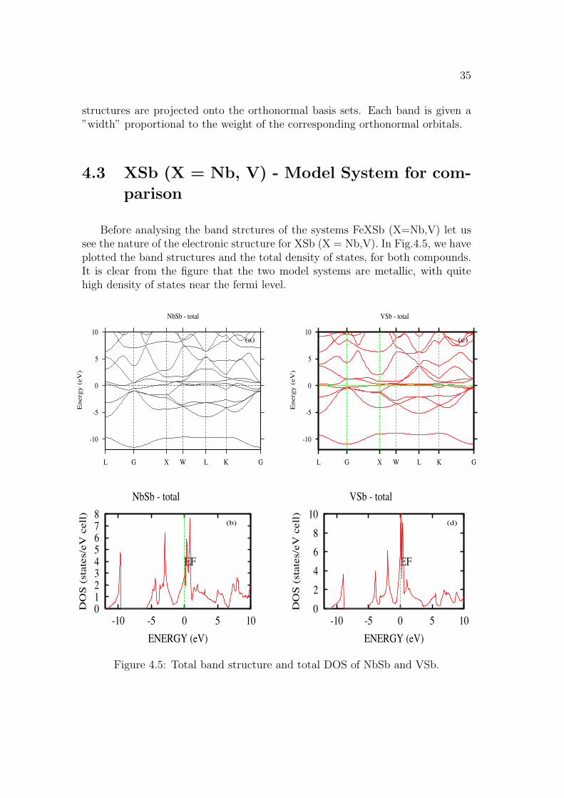
4.3 XSb (X = Nb, V) - Model System for com-parison
Before analysing the band strctures of the systems FeXSb (X=Nb,V) let ussee the nature of the electronic structure for XSb (X = Nb,V). In Fig.4.5, we haveplotted the band structures and the total density of states, for both compounds.It is clear from the figure that the two model systems are metallic, with quitehigh density of states near the fermi level.
-10
-5
0
5
10
L G X W L K G
Ene
rgy
(eV
)
VSb - total
012345678
-10 -5 0 5 10
DO
S (
stat
es/e
V c
ell)
ENERGY (eV)
NbSb - total
EF
02468
10
-10 -5 0 5 10
DO
S (
stat
es/e
V c
ell)
ENERGY (eV)
VSb - total
EF
-10
-5
0
5
10
L G X W L K G
Ene
rgy
(eV
)
NbSb - total
(a) (c)
(b) (d)
Figure 4.5: Total band structure and total DOS of NbSb and VSb.

36
In Fig.4.6. we have plotted the fat bands to understand the orbital compo-sition of the bands. Now, the lowest band in Fig. 4.6(a) is that of Sb-s orbitalwhich undergoes a strong $!$ bonding with the Nb-s orbital. This is because, theSb and Nb atoms are on the same plane at a distance of 5.5500 a.u. This can,very clearly be seen in the fat band structure of Sb-s and Nb-s orbitals shown inFig. 4.6. Similarly in VSb also we can see the s-s bonding between V and Sbatoms.
-10
-5
0
5
10
L G X W L K G
En
erg
y (
eV)
Sb-s in NbSb
-10
-5
0
5
10
L G X W L K G
En
erg
y (
eV)
Nb-s in NbSb
-10
-5
0
5
10
L G X W L K G
En
erg
y (
eV)
Sb-s in VSb
-10
-5
0
5
10
L G X W L K G
En
erg
y (
eV)
V-s in VSb
(a) (c)
(b) (d)
Figure 4.6: Partial band structure of Sb-s and Nb-s orbitals in NbSb and VSb.
Fig.4.7 shows the plot of Sb-p and Nb/V-eg (x2 " y2, 3z2 " r2) fat band struc-tures. The energy range between -6 eV to -2 eV is dominated by the Sb-p charac-

37
ter, in both the compounds. The fat band structure of the V and Nb shows thatthere exists a strong bonding between the Sb-p orbitals and the X-eg (X = V,Nb)orbitals that lie just above the fermi level. Most importantly the bands that lieclose to the Fermi level are the non-bonding Nb/V-t2g as shown in Fig.4.8.
-10
-5
0
5
10
L G X W L K G
En
erg
y (
eV)
Nb-eg in NbSb
-10
-5
0
5
10
L G X W L K G
En
erg
y (
eV)
Sb-p in NbSb
-10
-5
0
5
10
L G X W L K G
En
erg
y (
eV)
V-eg in VSb
-10
-5
0
5
10
L G X W L K G
En
erg
y (
eV)
Sb-p in VSb
(a) (b)
(c) (d)
Figure 4.7: Fat band structure of Sb-p and X-eg in NbSb and VSb.

38
4.4 FeNbSb / FeVSb
Let us now analyse the e"ect of inserting the Fe atoms into the NbSb andthe VSb system. It is seen that the Fe-d bands lie below the fermi level. TheseFe-d orbitals are found to interact with the Nb-d/V-d orbitals respectively. Inparticular, the fat band structure shows that the Nb-t2g/V-t2g orbitals are in-volved, which are pushed su!ciently up and now they lie above the fermi level.This opens up an enery gap and makes the system a direct narrow band gapsemiconductor.
-10
-5
0
5
10
L G X W L K G
Ene
rgy
(eV
)
Nb-t2g in FeNbSb
-10
-5
0
5
10
L G X W L K G
Ene
rgy
(eV
)
Fe-d in FeNbSb
-10
-5
0
5
10
L G X W L K G
Ene
rgy
(eV
)
Fe-d in FeVSb
-10
-5
0
5
10
L G X W L K G
Ene
rgy
(eV
)
V-t2g in FeVSb
(a) (b)
(c) (d)
Figure 4.8: Fat band structure of Nb/V-t2g and Fe-d orbitals in FeNbSb/FeVSb.

39
4.5 Origin of the gap formation
The preceeding analysis clearly shows that in the hypothetical compoundsNbSb/VSb there is a strong ! bonding between the Nb/V - eg orbitals with theSb-p orbitals, leading to bonding and antibonding states, thus getting pushedrespectively above and below the Fermi level. while the Nb/V-t2g levels are nonbonding and predominantly occupy the Fermi level. Now introduction of Feinduces a strong bonding between the Nb/V-t2g and the Fe-d states and open upa narrow gap in the half-Heusler compounds.
This narrow band gap is one of the crucial criteria for the material to be agood thermoelectric.
4.6 COHP
We shall now analyse these two systems with the help of COHP diagrams shown inFig.4.9 in which the dimensionless COHP is drawn along with the energy integralgiving the sum over all bonding, nonbonding, and antibonding interactions.
Fig.4.9(a) shows the o"site COHP contribution, between the neighbouringFe atoms seperated by a distance of 4.153 Angstroms in FeNbSb. Herein, wecan see bonding levels just below the fermi energy, at around -1 eV, seen as asharp negative COHP spike. Just ablove the fermi energy, at around 2 eV we seeantibonding levels also, seen as positive COHP spikes. Fig.4.9(b) shows the o"siteCOHP contribution between the adjacent Nb atoms also at a distance of 4.153Angstroms in FeNbSb. Comparing with the previous plot we see that, the integralCOHP is less negative for Fe-Fe bonding as compared to Nb-Nb bonding. TheCOHP between Fe-Sb atoms and Nb-Sb atoms are shown in Fig.4.9(c) and (d)respectively. In Fig.4.9(c), we have plotted the Nb-Fe d-d COHP. The bondinglevels are seen to dominate the energy range between -2 eV to -0.5 eV, and somefew antibonding levels above the fermi energy. The important point, that is to benoted here is that of the intergral COHP that is minimised for the real electroncount here, in contrast to the Nb-Nb and Fe-Fe contributions shown before. Bygeneral observation, we can conclude that, the Fe-Nb d-d bonding is the mainfactor that decides the band structure and also the origin of the band gap.

40
Fig.4.10 shows the similar plots of COHP and integrated COHP for the otherhalf-Heusler compound FeVSb. The trend remains the same for the other com-pound FeVSb, and by similar analysis Fe-V bonding is crucial for the gap forma-tion.

41
−12 −9 −6 −3 0 3 6 9−0.03 −0.03
−0.015 −0.015
0 0
0.015 0.015
ENERGY (eV)
CO
HP
(/ce
ll)
ICO
HP
(eV
/cel
l)
EF
Fe−Fe
−12 −9 −6 −3 0 3 6 9−3.4 −3.4
−2.9 −2.9
−2.4 −2.4
−1.9 −1.9
−1.4 −1.4
−0.9 −0.9
−0.4 −0.4
0.1 0.1
0.6 0.6
1.1 1.1
ENERGY (eV)
CO
HP
(/ce
ll)
ICO
HP
(eV
/cel
l)
EF
Fe − Nb
−12 −9 −6 −3 0 3 6 9−0.06 −0.06
−0.04 −0.04
−0.02 −0.02
0 0
0.02 0.02
0.04 0.04
0.06 0.06
0.08 0.08
0.1 0.1
ENERGY (eV)C
OH
P(/
cell)
ICO
HP
(eV
/cel
l)
EF
−12 −9 −6 −3 0 3 6 9−3 −3
−2 −2
−1 −1
0 0
1 1
ENERGY (eV)
CO
HP
(/ce
ll)
ICO
HP
(eV
/cel
l)
EF
−12 −9 −6 −3 0 3 6 9−1 −1
−0.75 −0.75
−0.5 −0.5
−0.25 −0.25
0 0
0.25 0.25
0.5 0.5
ENERGY (eV)
CO
HP
(/ce
ll)
ICO
HP
(eV
/cel
l)
Sb − Nb
EF
Nb - Nb
Fe - Sb
Figure 4.9: COHP and Integrated COHP for FeNbSb

42
−12 −9 −6 −3 0 3 6 9−0.04 −0.04
−0.02 −0.02
0 0
0.02 0.02
0.04 0.04
ENERGY (eV)
CO
HP
(/ce
ll)
ICO
HP
(eV
/cel
l)
EF
−12 −9 −6 −3 0 3 6 9−3 −3
−2 −2
−1 −1
0 0
1 1
ENERGY (eV)
CO
HP
(/ce
ll)
ICO
HP
(eV
/cel
l)
EF
Fe − V
−12 −9 −6 −3 0 3 6 9−0.06 −0.06
−0.04 −0.04
−0.02 −0.02
0 0
0.02 0.02
0.04 0.04
0.06 0.06
0.08 0.08
ENERGY (eV)C
OH
P(/
cell)
ICO
HP
(eV
/cel
l)
EF
V − V
−12 −9 −6 −3 0 3 6 9−2.5 −2.5
−2 −2
−1.5 −1.5
−1 −1
−0.5 −0.5
0 0
0.5 0.5
1 1
ENERGY (eV)
CO
HP
(/ce
ll)
ICO
HP
(eV
/cel
l)
EF
Fe − Sb
−12 −9 −6 −3 0 3 6 9−1.2 −1.2
−0.7 −0.7
−0.2 −0.2
0.3 0.3
ENERGY (eV)
CO
HP
(/ce
ll)
ICO
HP
(eV
/cel
l)
EF
V − Sb
Fe - Fe
Figure 4.10: COHP and Integrated COHP for FeVSb

43
4.7 Calculation of Seebeck Co-e!cient
To obtain the Seebeck potential or absolute thermoelectric power, we have pri-marily to detremine the electric field produced in the conductor when a temper-ature gradient is present and no current is permitted to flow in the circuit ( opencircuit conditions ). A general expression for the absolute thermoelectric poweris gven by,
S =
)
.x
dT/dx
*
Jx=0
"dg
dT(4.1)
where,
.x = Electric current
dT/dx = Temperature Gradient
Jx = Current Density
g = Thermodynamic (Gibbs) free energy per unit positive charge ofthe conduction charges in the material
If the conduction is by electrons, then
S =
)
.x
dT/dx
*
Jx=0
"1
e
d/
dT(4.2)
where,
/ = Gibbs free energy or fermi energy per conduction electron
Assuming that we are dealing with an isotropic free elctron gas, such that E= 1
2 m < v2 >, in the appproximation that the, mean free path is independantof the energy of the carrier (electron or hole), we get
)
.x
dT/dx
*
Jx=0
=2
3
Cel
e(4.3)
where,
Cel= Specific heat of the electron gas ="2k2
BTm
2*F
The above expression is independent of any particular assumptions about thestatistics of the electrons.

44
S =2
3
Cel
e"
1
e
d/
dT(4.4)
For a semiconductor, with the conducting electrons obeying ”Maxwellian”Statistics, we have
/ = kT ln(1
2Nh3(2m$kT )"3/2) (4.5)
S =
)
5
2
k
e"
/
eT
*
(4.6)
Here the relaxation time 0 rather than the mean free path is assumed to bea constant.Now we shall do a sample calculation for the half-Heusler compound FeNbSb. Allquantities in equations (4.5) and (4.6) are known except N, which is the numberof carriers per unit volume. This N is given by,
N =k3
F
3$2(4.7)
where,kF = Propagation vector.
From the band structure calculations, we get .F = fermi energy, using thatwe can calculate kF ,
h2k2F
2m= .F
which gives,
kF =+
2m.F
h3
,1/2
N =
-2m*F
h2
.3
3$2
Now we substitute this formula for N, and get the final value of the Seebeckco-e!cient.
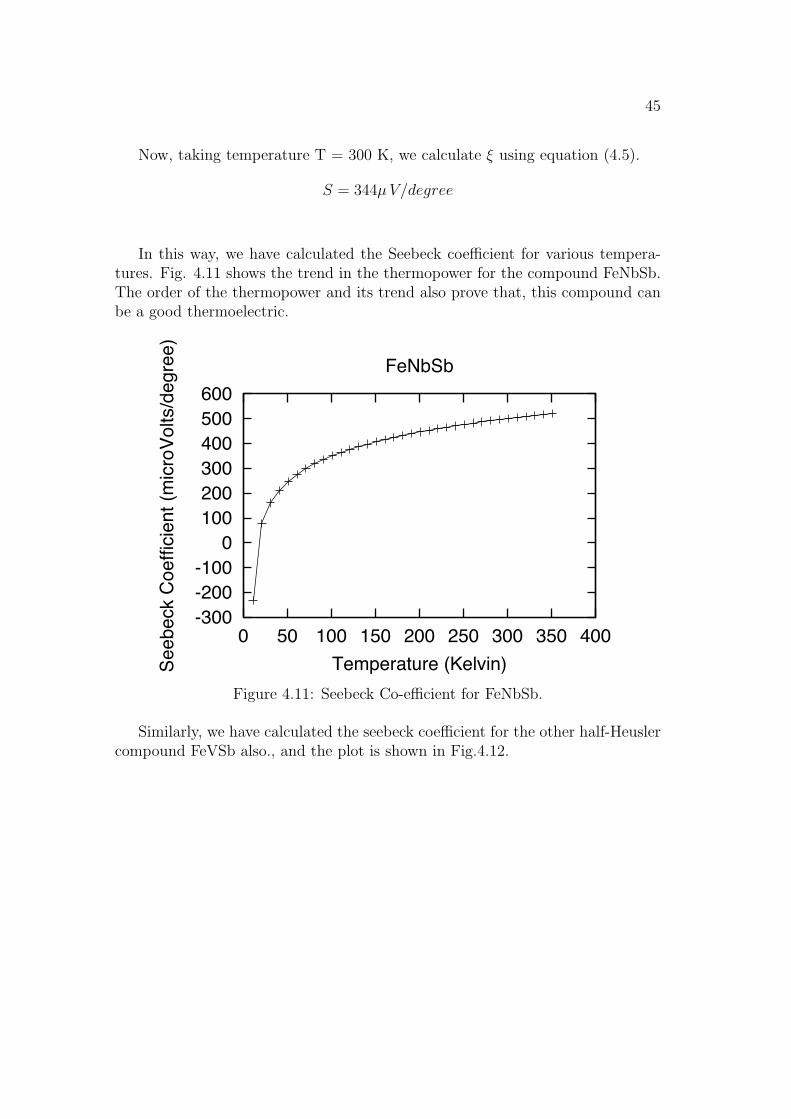
For FeNbSb, .F = 0.01049 eV
Therefore,N = 4.858738 ) 1024
45
Now, taking temperature T = 300 K, we calculate / using equation (4.5).
S = 344µV/degree
In this way, we have calculated the Seebeck coe!cient for various tempera-tures. Fig. 4.11 shows the trend in the thermopower for the compound FeNbSb.The order of the thermopower and its trend also prove that, this compound canbe a good thermoelectric.
-300-200-100
0100200300400500600
0 50 100 150 200 250 300 350 400
Seeb
eck
Coe
ffici
ent (
mic
roVo
lts/d
egre
e)
Temperature (Kelvin)
FeNbSb
Figure 4.11: Seebeck Co-e!cient for FeNbSb.
Similarly, we have calculated the seebeck coe!cient for the other half-Heuslercompound FeVSb also., and the plot is shown in Fig.4.12.

46
.
-300-200-100
0100200300400500600
0 50 100 150 200 250 300 350 400
Seeb
eck
Coe
ffici
ent (
mic
roVo
lts/d
egre
e)
Temperature (Kelvin)
FeVSb
Figure 4.12: Seebeck Co-e!cient for FeVSb.

Chapter 5
Study of Chevrel phases forpossible thermoelectricapplications
Widespread use of thermoelectric materials6, as an alternative technology for thepower generation and refrigeration, remains a desirable but elusive goal. Thee!ciency of the devices based on current state-of-the-art materials is low. Thislargely restricts them to the applications where the reliability outweighs e!-ciency or small devices are needed. A good thermoelectric material has highthermopower, a low lattice contribution to the thermal conductivity 1 and a size-able electric conductivity. The thermoelectric figure of merit is ZT = !S2T/1,where ! is the electrical conductivity, S is the Seebeck coe!cient (thermopower),and 1 = 1el +1latt is the thermal conductivity (1el and 1latt are the electronic andlattice contributions, respectively). Current thermoelectric materials have ZT *1. Large values of the S are typical of doped semiconductors, while ! is largein metals. Starting from a material with low 1, the above expression suggeststhat enhanced values of ZT can be obtained by searching for the compositionwhich maximise the power factor, !S2, with respect to the carrier concentrationn. An additional requirement arises from the Wiedemann-Franz law7, which setsa rough lower bound on the Lorentz number L = 1/!T [Lmin = ($21B/3e)]. Avalue of S + 160 µV/K is thus needed for ZT + 1, even if 1latt is negligibly small.Empirical evidence and minimum thermal conductivity theories imply that mate-rials having large numbers of atoms in the unit cell and large atomic masses (softphonons), are most likely to have the requisite low thermal conductivites. Hencein the recent years, the center of gravity of the search for new thermoelectric mate-
47

48
rials has moved towards crystallographically more complicated compounds. Thisis motivated in part by the fact that low values of thermal conductivity, needed forthermoelctric performance, are more likely in such materials, and partly becausesuch structures provide more avenues for chemical optimization. Good examplesare high figure of merit (ZT ) skutteridite and Zn-Sb thermoelectrics. Here weinvestigate the materials in the family of molybdenum (Mo) cluster compoundsknown as ‘Chevrelphases7,8,10. These are based on the binaries Mo6X8, where Xis a chalcogen (S, Se, Te). The crystal structure contains large voids, which maybe filled to yield a large variety of ternary compounds with the general formulaMxMo6X8, where M can be a simple or transition metal atom, or a rare-earth el-ement. This provides the oppurtunities for obtaining low thermal conductivities,analogous to skutterudites as well as a chemical knob for modifying the electronicproperties. These materials fulfill the requirements for low 1 outlined above.
5.1 Structure of Mo6X8
The arrangement of the host structure8 remains the same for all the compounds.It consists of a stacking of Mo6X8 building blocks. Each building block repre-sents a unit cell of Cu3Au structure type, i.e. a cube formed by eight chalcogensatoms which contains an octahedron of tightly packed molybdenum atoms. Theseatoms are slightly outside the middle of the faces of the X atom cube. The iso-lated Mo6X8 unit then has almost cubic symmetry. In the crystal, the cornersof each Mo6X8 cube lie directly opposite to the face centers of adjacent cubes.That means that there are close contacts between Mo atoms of one isolated unitand the chalcogen atoms of the other units (Fig. 5.1).
The unit cell is constructed as shown in Fig.5.2. The cation (inserted ina cavity described below) is in position (0 0 0) on the ternary axis. the otherinserted cations are distributed on the corners of the rhombohedral cell which hasan angle close to 90o. But the symmetry is not cubic, even if ( = 900, becausethe Mo6X8 building blocks are not parallel to the unit cell vectors but are turnedby an angle ) of about 27o around the ternary axis.The arrangement of these building blocks leaves, as said before, a certain numberof cavities in the chalcogen atom network. There are three types of cavities inth lattice (Fig.5.3) The largest one (site 1) is approximately cube shaped and isformed by eight chalcogen atoms formed by eight di"erent Mo6X8 units.

49
.
Figure 5.1: Building block arrangement.
(Mo-Mo) intercluster liasons and (Mo-X1) intercluster liasons are representedby dashed lines
Figure 5.2: Elementary cell of rhombohedral structure
Inserted cations are located in position (0,0,0), the unit block is turned by anangle of about 27o around the ternary axis.
Smaller cavities (site 2) are formed by eight chalcogen atoms belonging to fourdi"erent building blocks, and have a more irregular shape. the last type of cavity(site 3) is formed by eight chalcogen atoms belonging to two building blocks.

50
All these cavities are empty in the binary compounds Mo6X8 and are filled withcations in the ternary compounds MxMo6X8 (M = metal).
Figure 5.3: Projection on the hexagonal(1120) plane.
The three types of cavities are represented. Large cations are located in site 1.
The type of cavity filled depends mainly on the size of the cation. Large atoms(Pn, Sn,....) occupy site 1 (Fig. 5.3), and lead to a stoichiometric compound.Small atoms (Cu, Zn, Ni,...) are statistically distributed between sites 1 and 2(Fig.5.4), and lead to non-stoichiometric compound. The size and shape of thecavity depends on the nature of the inserted cation. It modifies the distancesbetween Mo atoms.
Now, having analysed the structure of a general chevrel phase Mo6X8, we shallconsider a particular chevrel phase Molybdenum Selenide Mo6Se8 and analyse itselectronic structure. As there is a close contact between the Mo atoms of one unitwith that of the chalcogen atoms of the other units, bonding takes place betweenthe p orbitals of selinium atoms and the d orbitals of the molybdenum atoms,thus giving rise to pd! bonding and antibonding levels, with a large gap betweenthe bonding and the antibonding levels. The molybdenum atoms that are tightlypacked in the octahedron also bond with each other, giving rise to a total oftwelve bonds. These twelve bonds in turn give rise to bonding and antibondinglevels seperated by a dd gap. There are 20 valence electrons involved in Mo6Se8,which falls short by 4 electrons to completely fill the bonding levels, thus making

51
.
Figure 5.4: Distribution of small cations in the lattice
Mo6Se8 a metal. But if we are able to dope it with an element that canprovide the needed 4 electrons then the bonding levels will get filled leading to arise in the Fermi level, that in turn will convert the material to a semiconductor,which in turn can be analysed for thermoelectric applications.
5.2 Details of LDA LMTO-ASA calculations
We have computed the band structure and the density of states of Mo6Se8.
5.2.1 Band Structure
The results got above are again confirmed with the band structure plots shown inFig.5.6. The portion of the bonding levels that are above the Fermi level becauseof scarcity of 4 electrons are clearly visible in figure.
5.2.2 Density of States
The results DOS is shown in Fig 5.5. Comparing Fig.5.5(b) and (c), it is clearthat a p-d bonding9 between Se and Mo has taken place, and the resultant p-d

52
-15
-10
-5
0
5
10
L Z G F
Energ
y (eV
)
Figure 5.5: Band structure of Mo6Se8
05
1015202530
-15 -10 -5 0 5 10
DO
S (s
tate
s/eV
cel
l)
ENERGY (eV)
EF
05
1015202530
-15 -10 -5 0 5 10
DO
S (s
tate
s/eV
cel
l)
ENERGY (eV)
EF
0
5
10
15
20
-15 -10 -5 0 5 10
DO
S (s
tate
s/eV
cel
l)
ENERGY (eV)
EF
0
2
4
6
8
10
-15 -10 -5 0 5 10
DO
S (s
tate
s/eV
cel
l)
ENERGY (eV)
EF
Mo6Se8 Mo-d
Se1-p Se2-p
(a) (b)
(c) (d)
Figure 5.6: Density of states of Mo6Se8.

53
gap is seen from -12 eV to -5 eV. The d-d gap arising because of Mo-Mobonding in the tightly packed octahedron is seen near the Fermi level.
5.3 SnMo6Se8
Now in order to push up the Fermi level, we tried doping Mo6X8 with Tin (Sn). Sngives an additional two electrons to the whole system, still leading to a deficiencyof two more.
5.3.1 Band Structure
The band structure got from the first principles calculations is showm above.On comparing Fig.5.7 and 5.6, it is clearly visible that there is a slight lift inthe Fermi level, caused by the addition of Sn to the chevrel phase. But stillthere are 2 more electrons needed to fill the bonding levels completely so thatthe compound turns in to a semiconductor. Thus SnMo6X8 is still a metal withunoccupied bonding levels.
-15
-10
-5
0
5
10
L Z G F
Ene
rgy (
eV)
Figure 5.7: Band structure of SnMo6Se8

54
5.3.2 Density of states
The density of states of SnMo6Se8 got from the LDA LMTO-ASA approximatonis plotted below. Analogous to Mo6Se8 we have a pd and a dd gap, however
05
10152025303540
-15 -10 -5 0 5 10
DO
S (
stat
es/e
V c
ell)
ENERGY (eV)
EF
05
1015202530
-15 -10 -5 0 5 10
DO
S (
stat
es/e
V c
ell)
ENERGY (eV)
EF
0
5
10
15
20
-15 -10 -5 0 5 10
DO
S (
stat
es/e
V c
ell)
ENERGY (eV)
EF
0
2
4
6
8
10
-15 -10 -5 0 5 10
DO
S (
stat
es/e
V c
ell)
ENERGY (eV)
EF
SnMo6Se8
Mo
Sn
Se1
(a) (b)
(c) (d)
Figure 5.8: Density of states of SnMo6Se8
now the fermi level is more close to the dd gap, because of the addition of twoelectrons.

55
5.4 E"ect of insertion of small cations
Next we tried inserting Mo6Se8 with small cation Copper (Cu). To obtaina periodic system we have chosen a given Cu1 and a given Cu2 as occupied, theother being empty. The six Mo atoms and the eight Se atoms become inequivalentand we have treated a 16 inequivalent atom unit cell.
5.4.1 Density of States
05
1015202530
-6 -4 -2 0 2 4
DO
S (
stat
es/e
V c
ell)
ENERGY (eV)
All
EF
0
5
10
15
20
-6 -4 -2 0 2 4
DO
S (
stat
es/e
V c
ell)
ENERGY (eV)
Cu-all
EF
0
5
10
15
20
-6 -4 -2 0 2 4
DO
S (
stat
es/e
V c
ell)
ENERGY (eV)
Mo-all
EF
0
5
10
15
20
-6 -4 -2 0 2 4
DO
S (
stat
es/e
V c
ell)
ENERGY (eV)
Se-all
EF
Figure 5.9: Density of States of Cu2Mo6Se8
Fig.5.9 shows the density of states plot for Cu2Mo6Se8 system. Comparingthis with that of the DOS plot for Mo6Se8 (Fig.5.6) we see that, there is a narrow

56
Cu-d band (at around -2.5 eV) which falls within the p-d (Mo-Se) band (around-2 eV ). Since these d states are filled anyway, the two valence electrons of thetwo Cu ions are in the p-d band and the compound is always conducting.
5.4.2 Band Structure
The band structure for Cu2Mo6Se8 system obtained from the self consistentLDA-LMTO-ASA calculations is shown in Fig.5.10. Here also we see the bandscrossing the Fermi level, thus proving that Cu2Mo6Se8 is a metallic system.
-6
-4
-2
0
2
4
L Z G F
En
erg
y (
eV)
Cu2Mo6Se8
Figure 5.10: Band structure of Cu2Mo6Se8

Chapter 6
Outlook
In this project we have used various indicators of chemical bonding within firstprinciples TB-LMTO ASA method to analyse the electronic structure and chem-ical bonding of various complex crystalline systems. We have mainly focuusedour analysis on systems that have been suggested to be possible canditates forgood thermoelectric applications.
We have calculated the electronic structure of two ternary intermetallic com-pounds with half-Heusler structure: FeVSb and FeNbSb. Based on our bandstructure calculations. we conclude the following,
• FeVSb/FeNbSb are small, indirect-gap semiconductors.
• Fe plays an important role in determing the band gap, which was confirmedusing the COHP plot.
Our calculations suggest that the half-Heusler compounds, ”FeVSb and FeNbSb”are quite prominsing for thermoelectric applications.
We have also presented the first principles electronic structure calculationsof Chevrel phases based on Mo6Se8 unit. But both SnMo6Se8 as well asCu2Mo6Se8 have a metallic behaviour. For the search for semiconducting com-positions inthe chevral phases family we suggest the alloying on the Mo sites withtransition metals like Re and Rh.
57

References
1. O.K. Andersen, O.Jepsen, and D. Glotzel, Highlights of condensed matter the-ory, ed. F. Bassani, F. Fumi and M.P. Tosi, (North Holland, Amsterdam),59.
2. G.P.Das, Pramana-J.Phys. 38, 545 (1992)
3. Adrian P.Sutton in Electronic Structure of Materials
4. H.L.Skriver in The LMTO method Mu!n-Tin orbitals and electronic structure(Springer-Verlag, 1984)
5. Richard Dronskowski and Peter E. Blochl, J. Phys. Chem. 97, 8617 (1993)
6. Gerald Mahan, Brian Sales and Je" Sharp, Phys. Today, 42 (1997)
7. R.W.Nunes, I.I.Mazin and D.J.Singh in Theoretical search for Chevrel phasesbased thermoelectric materials Phys. Rev B (1999).
8. C.Roche, et.al., J.Phys. Condens Matter 10, 335 (1998)
9. W.Klose and O.K.Andersen in SuperconductivityinTernaryCompoundsI Eds.O. Fischer and M.B.Maple (Spring-Verlag, 1982)
10. C.Roche, et.al., Phys.Rev. B60, 16442 (1999)
11. O.Jepsen, O.K.Andersen Z. Phys. B97, 35 (1995)
12. Walter R.L.Lambrecht, Niels E. Christensed and Peter Blochl, Phys.Rev.B36 35 (1987)
13. S.D. Mahanti, etal. in Electronic Structure of rare-earth nickel pnictides:Narrow-gap thermoelectric materials, Phys. Rev. B 59 24 (1999)
14. R.J. Cava, et al. Phys. Rev. B 87 1 (2000)
15. Ove Jepsen, et al. Journal of Solid State Chemistry 130, 254-265 (1997)
16. D.K.C. MacDonald, Thermoelectricity (Wiley, New York, 1962), p. 25.
58