fms2016 - nand flash basics - flash memory summit€¢ nand flash is currently unrivalled technology...
TRANSCRIPT
NAND Flash Basics & Error Characteristics
Why Do We Need Smart Controllers?
Thomas Parnell, IBM Research - Zurich
Flash Memory Summit 2016Santa Clara, CA 1
Agenda• Part I. NAND Flash Basics
• Device Architecture (2D + 3D)• SLC, MLC & TLC • Program/Read/Erase Procedure
• Part II. Error Characteristics• Program/erase cycling stress• Cell-to-cell Interference• Data Retention / Read Disturb • Programming Errors • 2D vs. 3D Reliability Comparison
Flash Memory Summit 2016Santa Clara, CA 2
Part I: NAND Flash Basics
Flash Memory Summit 2016Santa Clara, CA 3
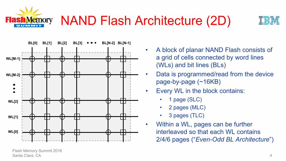
NAND Flash Architecture (2D)
• A block of planar NAND Flash consists of a grid of cells connected by word lines (WLs) and bit lines (BLs)
• Data is programmed/read from the device page-by-page (~16KB)
• Every WL in the block contains:• 1 page (SLC)• 2 pages (MLC)• 3 pages (TLC)
• Within a WL, pages can be further interleaved so that each WL contains 2/4/6 pages (“Even-Odd BL Architecture”)
Flash Memory Summit 2016Santa Clara, CA 4
WL[0]
WL[1]
WL[2]
WL[M-2]
WL[M-1]
BL[0] BL[1] BL[2] BL[3] BL[N-2] BL[N-1]
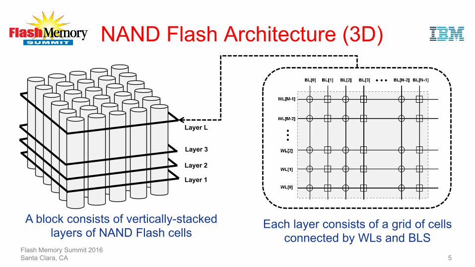
NAND Flash Architecture (3D)
Flash Memory Summit 2016Santa Clara, CA 5
A block consists of vertically-stacked layers of NAND Flash cells
Layer L
Layer 3
Layer 1
Layer 2
Each layer consists of a grid of cells connected by WLs and BLS
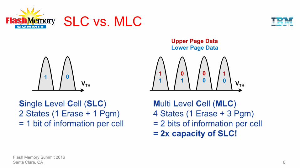
SLC vs. MLC
Flash Memory Summit 2016Santa Clara, CA 6
1 0VTH
11
01 VTH
00
10
Single Level Cell (SLC)2 States (1 Erase + 1 Pgm)= 1 bit of information per cell
Multi Level Cell (MLC)4 States (1 Erase + 3 Pgm)= 2 bits of information per cell= 2x capacity of SLC!
Upper Page DataLower Page Data
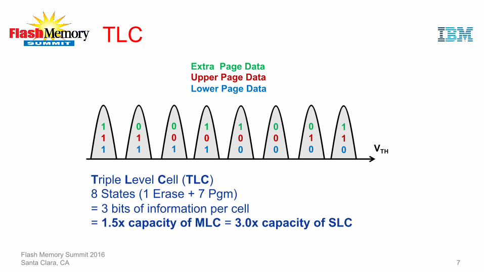
TLC
Flash Memory Summit 2016Santa Clara, CA 7
111
011 VTH
001
101
Extra Page DataUpper Page DataLower Page Data
100
000
010
110
Triple Level Cell (TLC)8 States (1 Erase + 7 Pgm)= 3 bits of information per cell= 1.5x capacity of MLC = 3.0x capacity of SLC
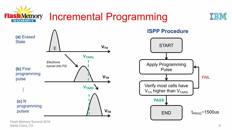
Incremental Programming
Flash Memory Summit 2016Santa Clara, CA 8
VTHE
VTH
VTARG
VTH
VTARG
(c) N programming pulses
(b) First programming pulse
(a) Erased State
Apply Programming Pulse
Verify most cells have VTH higher than VTARG
START
PASS
FAIL
END
ISPP Procedure
Electrons tunnel into FG
…
tPROG~1500us
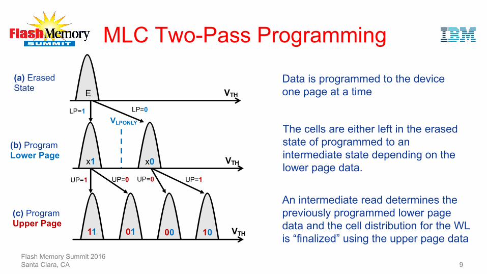
MLC Two-Pass Programming
Flash Memory Summit 2016Santa Clara, CA 9
VTH
VTH11 01 00 10
x1 x0
(c) Program Upper Page
(b) Program Lower Page
VTHE
LP=0LP=1
UP=1 UP=0 UP=0 UP=1
(a) Erased State
VLPONLYThe cells are either left in the erased state of programmed to an intermediate state depending on the lower page data.
An intermediate read determines the previously programmed lower page data and the cell distribution for the WL is “finalized” using the upper page data
Data is programmed to the device one page at a time

Reading Data Back (MLC)
Flash Memory Summit 2016Santa Clara, CA 10
• Lower page can be read using a single read voltage (VB)• Upper page can be read using a pair of read voltages (VA,VC)• A page read typically takes up to 100us
VTH11 01 00 10
VBDetect LP =1 Detect LP =0
Lower Page Read
VTH11 01 00 10
VA
Upper Page Read
VCDetect UP =0 Detect UP=1Detect UP=1
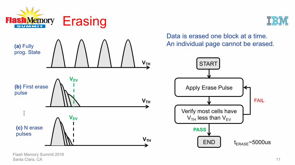
Erasing
Flash Memory Summit 2016Santa Clara, CA 11
VTH
VEV
Apply Erase Pulse
Verify most cells have VTH less than VEV
START
VEV
PASS
FAIL
(c) N erase pulses
(b) First erase pulse
(a) Fullyprog. State
…
VTH
VTH
Data is erased one block at a time.An individual page cannot be erased.
END tERASE~5000us
Part II: Error Characteristics
Flash Memory Summit 2016Santa Clara, CA 12
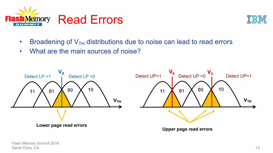
Read Errors• Broadening of VTH distributions due to noise can lead to read errors• What are the main sources of noise?
Flash Memory Summit 2016Santa Clara, CA 13
VTH
11 01 00 10
VBDetect LP =1 Detect LP =0
VTH
11 01 00 10
VA VCDetect UP =0 Detect UP=1Detect UP=1
Lower page read errorsUpper page read errors
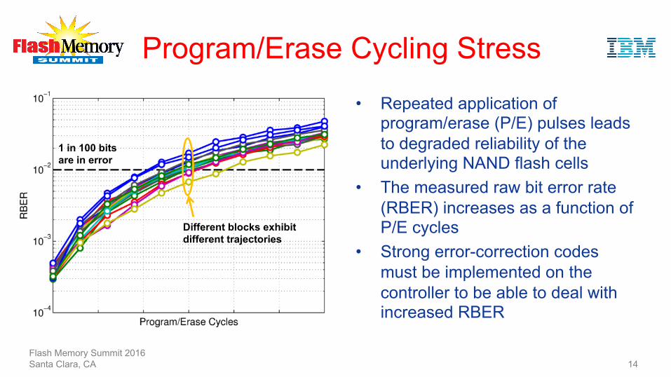
Program/Erase Cycling Stress• Repeated application of
program/erase (P/E) pulses leads to degraded reliability of the underlying NAND flash cells
• The measured raw bit error rate (RBER) increases as a function of P/E cycles
• Strong error-correction codes must be implemented on the controller to be able to deal with increased RBER
Flash Memory Summit 2016Santa Clara, CA 14
1 in 100 bits are in error
Different blocks exhibit different trajectories
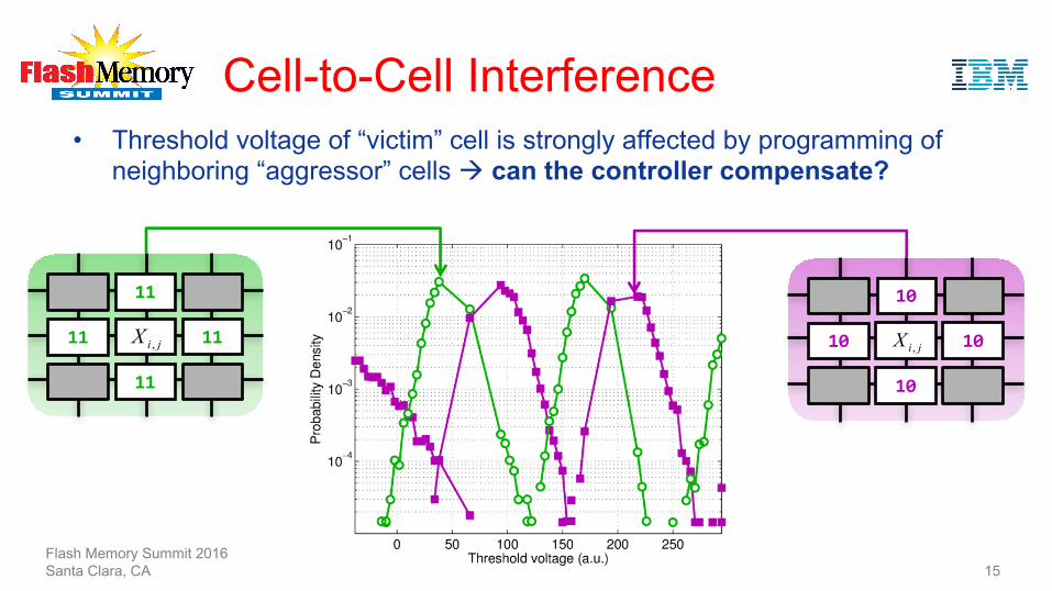
Cell-to-Cell Interference
Flash Memory Summit 2016Santa Clara, CA 15
• Threshold voltage of “victim” cell is strongly affected by programming of neighboring “aggressor” cells à can the controller compensate?
jiX ,
11
11
11 11jiX ,
10
10
10 10
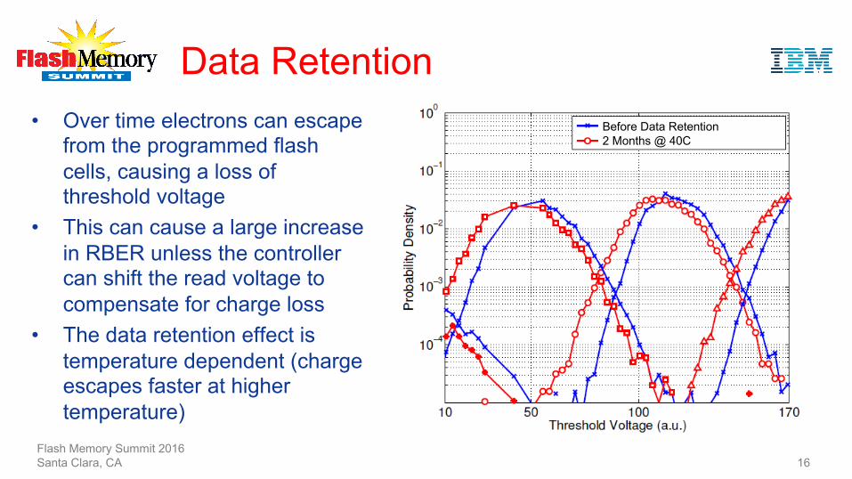
Data Retention • Over time electrons can escape
from the programmed flash cells, causing a loss of threshold voltage
• This can cause a large increase in RBER unless the controller can shift the read voltage to compensate for charge loss
• The data retention effect is temperature dependent (charge escapes faster at higher temperature)
Flash Memory Summit 2016Santa Clara, CA 16
Before Data Retention2 Months @ 40C
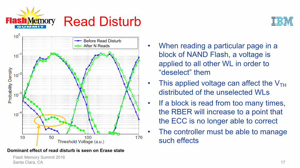
Read Disturb
Flash Memory Summit 2016Santa Clara, CA 17
• When reading a particular page in a block of NAND Flash, a voltage is applied to all other WL in order to “deselect” them
• This applied voltage can affect the VTHdistributed of the unselected WLs
• If a block is read from too many times, the RBER will increase to a point that the ECC is no longer able to correct
• The controller must be able to manage such effects
Before Read DisturbAfter N Reads
Dominant effect of read disturb is seen on Erase state

Programming Errors
18
Cells are programmed to the wrong state!
• Degradation of erase state can cause error propagation during the two-pass programming procedure à switch to 1-pass?
Flash Memory Summit 2016Santa Clara, CA
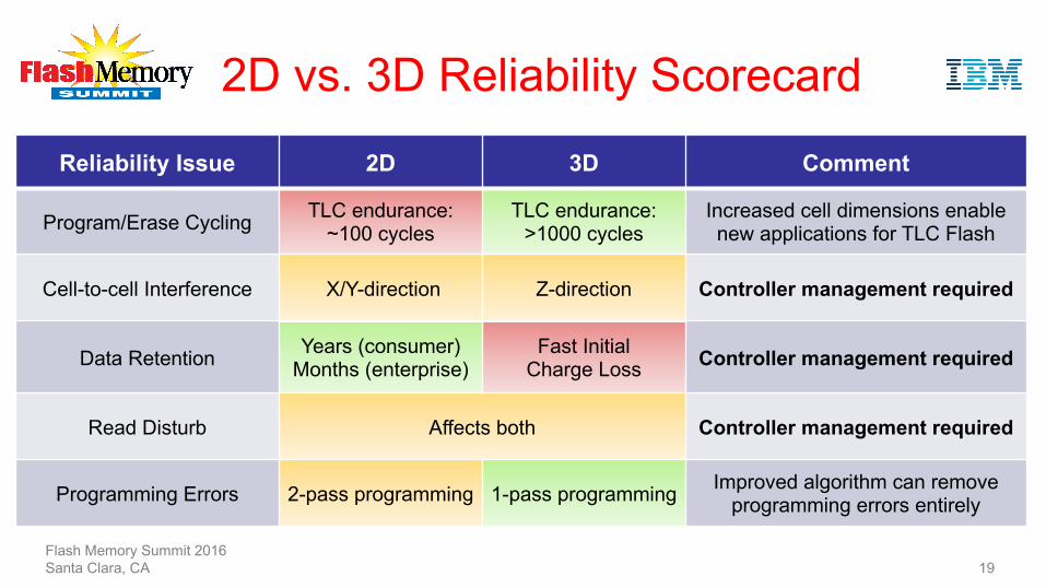
2D vs. 3D Reliability Scorecard
Flash Memory Summit 2016Santa Clara, CA 19
Reliability Issue 2D 3D Comment
Program/Erase Cycling TLC endurance: ~100 cycles
TLC endurance: >1000 cycles
Increased cell dimensions enable new applications for TLC Flash
Cell-to-cell Interference X/Y-direction Z-direction Controller management required
Data Retention Years (consumer)Months (enterprise)
Fast Initial Charge Loss Controller management required
Read Disturb Affects both Controller management required
Programming Errors 2-pass programming 1-pass programming Improved algorithm can remove programming errors entirely
Conclusions• NAND Flash is currently unrivalled technology in terms of
the performance/cost trade-off • However, it is inherently unreliable and cannot be used
without a controller providing additional functionality • What do we require of a controller?
• Media management / signal processing • Powerful error-correction • Data placement/management algorithms • Efficient FPGA/ASIC/firmware implementations
Flash Memory Summit 2016Santa Clara, CA 20