fms6146 - fairchild semiconductor
TRANSCRIPT

To learn more about ON Semiconductor, please visit our website at www.onsemi.com
Please note: As part of the Fairchild Semiconductor integration, some of the Fairchild orderable part numbers will need to change in order to meet ON Semiconductor’s system requirements. Since the ON Semiconductor product management systems do not have the ability to manage part nomenclature that utilizes an underscore (_), the underscore (_) in the Fairchild part numbers will be changed to a dash (-). This document may contain device numbers with an underscore (_). Please check the ON Semiconductor website to verify the updated device numbers. The most current and up-to-date ordering information can be found at www.onsemi.com. Please email any questions regarding the system integration to [email protected].
Is Now Part of
ON Semiconductor and the ON Semiconductor logo are trademarks of Semiconductor Components Industries, LLC dba ON Semiconductor or its subsidiaries in the United States and/or other countries. ON Semiconductor owns the rights to a number of patents, trademarks, copyrights, trade secrets, and other intellectual property. A listing of ON Semiconductor’s product/patent coverage may be accessed at www.onsemi.com/site/pdf/Patent-Marking.pdf. ON Semiconductor reserves the right to make changes without further notice to any products herein. ON Semiconductor makes no warranty, representation or guarantee regarding the suitability of its products for any particular purpose, nor does ON Semiconductor assume any liability arising out of the application or use of any product or circuit, and specifically disclaims any and all liability, including without limitation special, consequential or incidental damages. Buyer is responsible for its products and applications using ON Semiconductor products, including compliance with all laws, regulations and safety requirements or standards, regardless of any support or applications information provided by ON Semiconductor. “Typical” parameters which may be provided in ON Semiconductor data sheets and/or specifications can and do vary in different applications and actual performance may vary over time. All operating parameters, including “Typicals” must be validated for each customer application by customer’s technical experts. ON Semiconductor does not convey any license under its patent rights nor the rights of others. ON Semiconductor products are not designed, intended, or authorized for use as a critical component in life support systems or any FDA Class 3 medical devices or medical devices with a same or similar classification in a foreign jurisdiction or any devices intended for implantation in the human body. Should Buyer purchase or use ON Semiconductor products for any such unintended or unauthorized application, Buyer shall indemnify and hold ON Semiconductor and its officers, employees, subsidiaries, affiliates, and distributors harmless against all claims, costs, damages, and expenses, and reasonable attorney fees arising out of, directly or indirectly, any claim of personal injury or death associated with such unintended or unauthorized use, even if such claim alleges that ON Semiconductor was negligent regarding the design or manufacture of the part. ON Semiconductor is an Equal Opportunity/Affirmative Action Employer. This literature is subject to all applicable copyright laws and is not for resale in any manner.

© 2006 Fairchild Semiconductor Corporation www.fairchildsemi.comFMS6146 • Rev. 1.1.0
October 2009
FMS6146 —
Low-C
ost Six-Channel 4th-O
rder Standard Defi nition Video Filter D
river
FMS6146Low-Cost Six-Channel 4th-OrderStandard Defi nition Video Filter DriverFeatures
Six 4th-Order 8MHz (SD) FiltersDrives Single, AC- or DC-Coupled, Video Loads (2Vpp, 150Ω)Drives Dual, AC- or DC-Coupled, Video Loads (2Vpp, 75Ω)Transparent Input ClampingAC- or DC-Coupled InputsAC- or DC-Coupled OutputsDC-Coupled Outputs Eliminate AC-Coupling Capacitors5V OnlyRobust 8kV ESD ProtectionLead-free TSSOP-14 Package
ApplicationsCable Set-Top BoxesSatellite Set-Top BoxesDVD PlayersHDTVPersonal Video Recorders (PVR)Video On Demand (VOD)
■
■
■
■
■
■
■
■
■
■
■
■
■
■
■
■
DescriptionThe FMS6146 Low-Cost Video Filter (LCVF) is intended to replace passive LC fi lters and drivers with a low-cost integrated device. Six 4th-order fi lters provide improved image quality compared to typical 2nd or 3rd-order passive solutions.
The FMS6146 may be directly driven by a DC-coupled DAC output or an AC-coupled signal. Internal diode clamps and bias circuitry may be used if AC-coupled inputs are required (see the Applications section for details).
The outputs can drive AC- or DC-coupled single (150Ω) or dual (75Ω) loads. DC coupling the outputs removes the need for output coupling capacitors. The input DC levels are offset approximately +280mV at the output (see the Applications section for details).
Ordering InformationPart Number Operating
Temperature Range Eco Status Package Packaging Method
FMS6146MTC14X -40°C to +85°C RoHS TSSOP-14 Tape and Reel
Functional Block DiagramIN1
IN2
IN3
IN4
IN5
IN6
OUT1
OUT2
OUT3
OUT4
OUT5
OUT6
8MHz, 4th order
6dBTransparent Clamp
6dBTransparent Clamp
6dBTransparent Clamp
6dBTransparent Clamp
6dBTransparent Clamp
6dBTransparent Clamp
For Fairchild’s defi nition of Eco Status, please visit: http://www.fairchildsemi.com/company/green/rohs_green.html.

© 2006 Fairchild Semiconductor Corporation www.fairchildsemi.comFMS6146 • Rev. 1.1.0 2
FMS6146 —
Low-C
ost Six-Channel 4th-O
rder Standard Defi nition Video Filter D
river
Pin Confi guration
FMS614614-pin
TSSOP
IN1 OUT1
IN2
IN3 OUT3
VCC
IN4
IN5
IN6
OUT2
GND
OUT5
OUT6
OUT4
1
2
3
4
5
6
7
14
13
12
11
10
9
8
Pin AssignmentsPin# Pin Name Type Description
1 IN1 Input Video input, Channel 1
2 IN2 Input Video input, Channel 2
3 IN3 Input Video input, Channel 3
4 VCC Input +5V supply, do not fl oat
5 IN4 Input Video input, Channel 4
6 IN5 Input Video input, Channel 5
7 IN6 Input Video input, Channel 6
8 OUT6 Output Filtered video output, Channel 6
9 OUT5 Output Filtered video output, Channel 5
10 OUT4 Output Filtered video output, Channel 4
11 GND Output Must be tied to ground, do not fl oat
12 OUT3 Output Filtered video output, Channel 3
13 OUT2 Output Filtered video output, Channel 2
14 OUT1 Output Filtered video output, Channel 1

© 2006 Fairchild Semiconductor Corporation www.fairchildsemi.comFMS6146 • Rev. 1.1.0 3
FMS6146 —
Low-C
ost Six-Channel 4th-O
rder Standard Defi nition Video Filter D
river
Absolute Maximum RatingsStresses exceeding the absolute maximum ratings may damage the device. The device may not function or be operable above the recommended operating conditions and stressing the parts to these levels is not recommended. In addition, extended exposure to stresses above the recommended operating conditions may affect device reliability. The absolute maximum ratings are stress ratings only.
Parameter Min. Max. UnitDC Supply Voltage -0.3 6 V
Analog and Digital I/O -0.3 VCC + 0.3 V
Output Channel - Any One Channel (Do Not Exceed) 50 mA
Reliability InformationSymbol Parameter Min. Typ. Max. Unit
TJ Junction Temperature +150 °C
TSTG Storage Temperature Range -65 +150 °C
TL Lead Temperature (Soldering, 10 seconds) +300 °C
ΘJAThermal Resistance, JEDEC Standard Multi-layer Test Boards, Still Air
90 °C/W
Electrostatic Discharge InformationSymbols Parameter Max. Unit
ESDHuman Body Model, JESD22-A114 4
kVCharged Device Model, JESD22-C101 2
Recommended Operating ConditionsThe Recommended Operating Conditions table defi nes the conditions for actual device operation. Recommended ope-rating conditions are specifi ed to ensure optimal performance to the datasheet specifi cations. Fairchild does not recom-mend exceeding them or designing to absolute maximum ratings.
Parameter Min. Typ. Max. UnitOperating Temperature Range -40 +85 °C
VCC Range +4.75 +5.0 +5.25 V

© 2006 Fairchild Semiconductor Corporation www.fairchildsemi.comFMS6146 • Rev. 1.1.0 4
FMS6146 —
Low-C
ost Six-Channel 4th-O
rder Standard Defi nition Video Filter D
river
DC Electrical CharacteristicsTA = 25°C, VCC = 5V, RSOURCE = 37.5Ω; all inputs are AC coupled with 0.1μF; all outputs are AC coupled with 220μF into 150Ω loads; unless otherwise noted.
Symbol Parameter Conditions Min. Typ. Max. Units ICC Supply Current(1) FMS6146 (No Load) 35 55 mA VIN Video Input Voltage Range Referenced to GND if DC coupled 1.4 Vpp PSRR Power Supply Rejection DC (All Channels) -50 dB
Note: 100% tested at 25°C.
AC Electrical CharacteristicsTA = 25°C, VIN = 1Vpp, VCC = 5V, RSOURCE = 37.5Ω; all inputs are AC coupled with 0.1μF; all outputs are AC coupled with 220μF into 150Ω loads; unless otherwise noted.
Symbol Parameter Conditions Min. Typ. Max. Units AV Channel Gain(1) All Channels 6.0 6.2 6.4 dB f1dB -1dB Bandwidth(1) All Channels 4.5 6.8 MHz fc -3dB Bandwidth All Channels 7.8 MHz fSB Attenuation (Stopband Reject) All Channels at f = 27MHz 48 dB
dG Differential Gain All Channels 0.3 % dφ Differential Phase All Channels 0.6 ° THD Output Distortion (All Channels) VOUT = 1.8Vpp, 1MHz 0.4 %
XTALK Crosstalk (Channel-to-Channel) at 1MHz -60 dB
SNR Signal-to-Noise Ratio All ChannelsNTC-7 Weighting: 100kHz to 4.2MHz 75 dB
tpd Propagation Delay Delay from Input-to-Output, 4.5MHz 59 ns
Note: 100% tested at 25°C.
1.
1.
© 2006 Fairchild Semiconductor Corporation www.fairchildsemi.comFMS6146 • Rev. 1.1.0 5
FMS6146 —
Low-C
ost Six-Channel 4th-O
rder Standard Defi nition Video Filter D
river
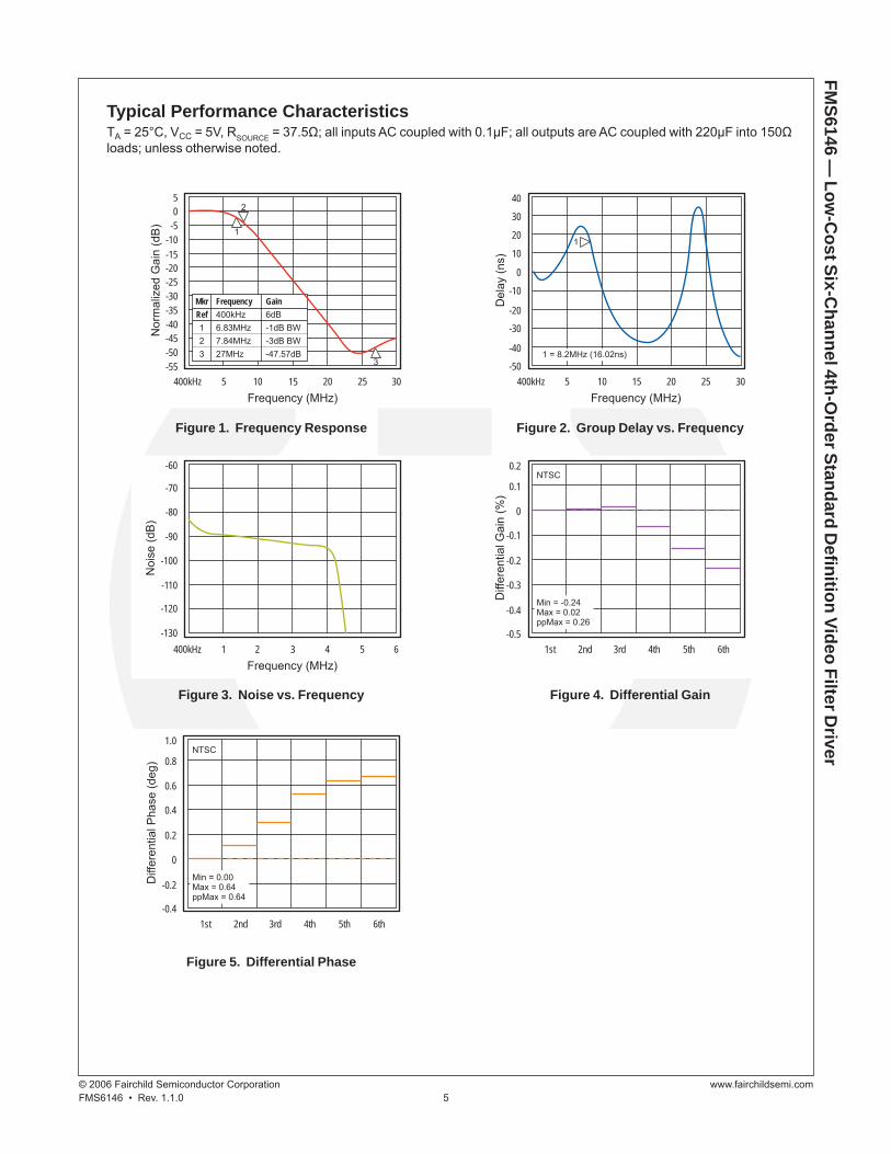
Typical Performance CharacteristicsTA = 25°C, VCC = 5V, RSOURCE = 37.5Ω; all inputs AC coupled with 0.1μF; all outputs are AC coupled with 220μF into 150Ω loads; unless otherwise noted.
1 = 8.2MHz (16.02ns)
1
-50
-40
-30
-20
-10
0
40
Del
ay (n
s)
400kHz 5 10 15 2520 30Frequency (MHz)
30
10
20
3
2
Nor
mal
ized
Gai
n (d
B)
400kHz 5 10 15 2520 30Frequency (MHz)
50
-5-10-15-20-25-30-35-40-45-50-55
1
Mkr Frequency Gain Ref 400kHz 6dB 1 6.83MHz -1dB BW 2 7.84MHz -3dB BW 3 27MHz -47.57dB
-0.5
-0.4
-0.3
-0.2
0.2
Diff
eren
tial G
ain
(%)
1st 2nd 3rd 5th4th 6th
0.1
-0.1
0
-60
Noi
se (d
B)
400kHz 1 2 3 54 6Frequency (MHz)
-70
-80
-90
-100
-110
-120
-130
NTSC
Min = -0.24Max = 0.02ppMax = 0.26
-0.4
-0.2
0
0.2
1.0
Diff
eren
tial P
hase
(deg
)
1st 2nd 3rd 5th4th 6th
0.8
0.4
0.6
NTSC
Min = 0.00Max = 0.64ppMax = 0.64
Figure 5. Differential Phase
Figure 3. Noise vs. Frequency Figure 4. Differential Gain
Figure 1. Frequency Response Figure 2. Group Delay vs. Frequency
© 2006 Fairchild Semiconductor Corporation www.fairchildsemi.comFMS6146 • Rev. 1.1.0 6
FMS6146 —
Low-C
ost Six-Channel 4th-O
rder Standard Defi nition Video Filter D
river
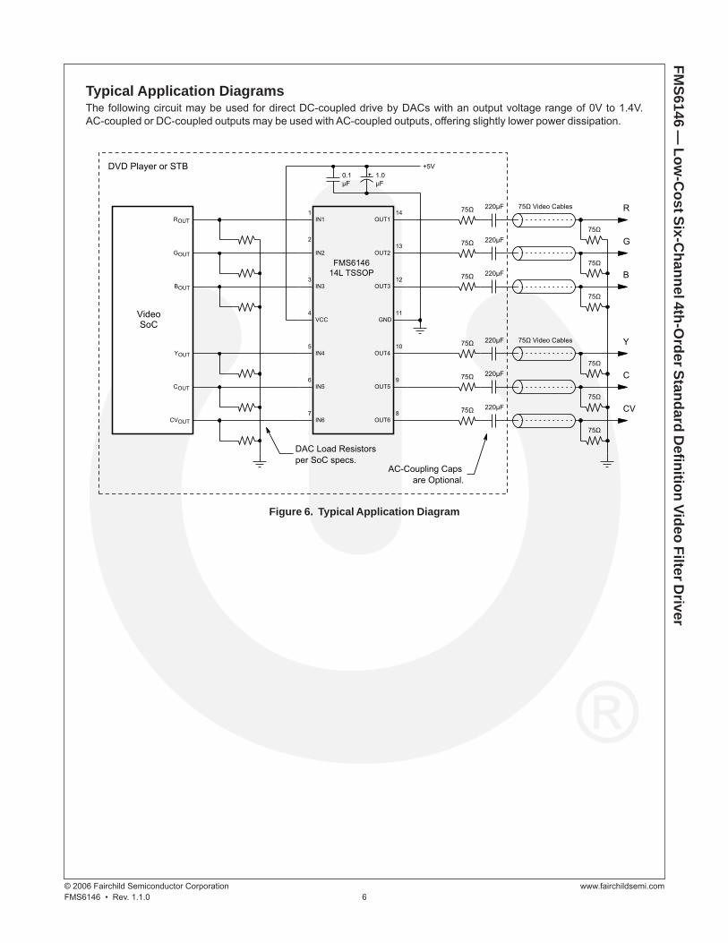
Typical Application DiagramsThe following circuit may be used for direct DC-coupled drive by DACs with an output voltage range of 0V to 1.4V. AC-coupled or DC-coupled outputs may be used with AC-coupled outputs, offering slightly lower power dissipation.
Figure 6. Typical Application Diagram
75Ω
220μF
220μF
220μF
+5V
FMS614614L TSSOP
IN1 OUT1
IN2
IN3 OUT3
VCC
IN4 OUT4
OUT6
14
13
12
11
10
9
8
1
2
3
4
5
6
7
IN5
IN6
OUT2
GND
OUT5
0.1μF
1.0μF
75Ω
75Ω
75Ω
75Ω
75Ω
220μF
75Ω
75Ω 75Ω Video Cables
220μF
75Ω
75Ω 75Ω Video Cables
220μF
75Ω
75Ω
VideoSoC
ROUT
BOUT
YOUT
CVOUT
GOUT
COUT
DAC Load Resistors per SoC specs.
AC-Coupling Caps are Optional.
DVD Player or STB
R
G
B
Y
C
CV

© 2006 Fairchild Semiconductor Corporation www.fairchildsemi.comFMS6146 • Rev. 1.1.0 7
FMS6146 —
Low-C
ost Six-Channel 4th-O
rder Standard Defi nition Video Filter D
river
Application InformationApplication CircuitsThe FMS6146 Low Cost Video Filter (LCVF) provides 6dB gain from input to output. In addition, the input is slightly offset to optimize the output driver performance. The offset is held to the minimum required value to decrease the standing DC current into the load. Typical voltage levels are shown in the diagram below:
There is a 280mV offset from the DC input level to theDC output level. VOUT = 2 * VIN + 280mV.
0.0 -> 0.02V0.3 -> 0.32V
0.65 -> 0.67V
1.0 -> 1.02V
VIN
0.28V0.88V
1.58V
2.28VDriven by: DC-Coupled DAC OutputsAC-Coupled and ClampedY, CV, R, G, B
VOUT
0.15V
0.5V
0.85V
VIN
0.58V
1.28V
1.98VDriven by: AC-Coupled and Biased U, V, Pb, Pr, C
VOUT
Figure 7. Typical Voltage Levels The FMS6146 provides an internal diode clamp to sup-port AC-coupled input signals. If the input signal does not go below ground, the input clamp does not operate. This allows DAC outputs to directly drive the FMS6146 without an AC coupling capacitor. When the input is AC coupled, the diode clamp sets the sync tip (or lowest voltage) just below ground. The worst-case sync tip compression due to the clamp cannot exceed 7mV. The input level set by the clamp, combined with the internal DC offset, keeps the output within its acceptable range.
For symmetric signals like Chroma, U, V, Pb, and Pr, the average DC bias is fairly constant and the inputs can be AC coupled with the addition of a pull-up resistor to set the DC input voltage. DAC outputs can also drive these same signals without the AC coupling capacitor. A conceptual illustration of the input clamp circuit is shown in Figure 8.
YOUT
Video Cables
Video Cables
75Ω
75Ω
75Ω
75ΩDriverYIN LOAD1
LOAD2(optional)
0.65V
Figure 8. Input Clamp Circuit
I/O Confi gurationsFor a DC-coupled DAC drive with DC-coupled outputs, use the confi guration shown in Figure 9.
DVD or STBSoCDAC
Output
75ΩLCVFClampInactive
0V - 1.4V
Figure 9. DC-Coupled Inputs and OutputsAlternatively, if the DAC’s average DC output level causes the signal to exceed the range of 0V to 1.4V, it can be AC coupled as shown in Figure 10.
DVD or STBSoCDAC
Output
LCVFClampActive
0.1μ
0V - 1.4V
75Ω
Figure 10. AC-Coupled Inputs, DC-Coupled Outputs
When the FMS6146 is driven by an unknown external source or a SCART switch with its own clamping circuitry, the inputs should be AC coupled as shown in Figure 11.
75ΩLCVFClampActive
0.1μExternal video source must be AC-coupled
0V - 1.4V
75Ω
Figure 11. SCART with DC-Coupled Outputs

© 2006 Fairchild Semiconductor Corporation www.fairchildsemi.comFMS6146 • Rev. 1.1.0 8
FMS6146 —
Low-C
ost Six-Channel 4th-O
rder Standard Defi nition Video Filter D
river
The same method can be used for biased signals, with the addition of a pull-up resistor to make sure the clamp never operates. The internal pull-down resistance is 800kΩ ±20%, so the external resistance should be 7.5MΩ to set the DC level to 500mV as shown in Figure 12.
LCVFBiasInput
0.1μ
External video source must be AC-coupled
500mV +/-350mV
75Ω7.5MΩ
75Ω
Figure 12. Biased SCART with DC-Coupled Outputs
The same circuits can be used with AC-coupled outputs if desired.
DVD or STBSoCDAC
Output
LCVFClampActive
0.1μ
0V - 1.4V
75Ω 220μ
Figure 13. DC-Coupled Inputs, AC-Coupled Outputs
DVD or STBSoCDAC
Output
75ΩLCVFClampActive
0.1μ
0V - 1.4V
220μ
Figure 14. AC-Coupled Inputs and Outputs
Figure 15. Biased SCART with AC-Coupled Outputs
NOTE: The video tilt or line time distortion is dominated by the AC-coupling capacitor. The value may need to be incre-ased beyond 220μF to obtain satisfactory operation in some applications.
Power DissipationThe FMS6146 output drive confi guration must be considered when calculating overall power dissipation. Care must be taken not to exceed the maximum die junction temperature. The following example can be used to calculate the FMS6146’s power dissipation and internal temperature rise.
Tj = TA + Pd • θJA EQ. 1
where: Pd = PCH1 + PCH2 + PCH3 and EQ. 2
PCHx = VCC • ICH - (VO2/RL) EQ. 3
where: VO = 2VIN + 0.280V EQ. 4
ICH = (ICC/3) + (VO/RL) EQ. 5
VIN = RMS value of input signal
ICC = 35mA
VCC = 5V
RL = channel load resistance
Board layout can also affect thermal characteristics. Refer to Layout Considerations for more information.
The FMS6146 is specifi ed to operate with output currents typically less than 50mA, more than suffi cient for a dual (75Ω) video load. Internal amplifi ers are current limited to a maximum of 100mA and should withstand brief-duration short-circuit conditions; this capability is not guaranteed.
LCVFClampActive
0.1μ
External video source must be AC-Coupled
0V - 1.4V
220μ75Ω
75Ω

© 2006 Fairchild Semiconductor Corporation www.fairchildsemi.comFMS6146 • Rev. 1.1.0 9
FMS6146 —
Low-C
ost Six-Channel 4th-O
rder Standard Defi nition Video Filter D
river
Layout ConsiderationsGeneral layout and supply bypassing play major roles in high-frequency performance and thermal characteristics. Fairchild offers a demonstration board, FMS6146DEMO, to guide layout and aid device testing and characterizati-on. The FMS6146DEMO is a four-layer board with full power and ground planes. Following this layout confi gu-ration provides the optimum performance and thermal characteristics. For optimum results, follow the guidelines below as a basis for high-frequency layout:
Include 1μF and 0.1μF ceramic bypass capacitors.
Place the 1μF capacitor within 0.75 inches of the power pin.
Place the 0.1μF capacitor within 0.1 inches of the power pin.
For multi-layer boards, use a large ground plane to help dissipate heat.
For two-layer boards, use a ground plane that extends beyond the device by at least 0.5 inches.
Minimize all trace lengths to reduce series inductances.
■
■
■
■
■
■
Output ConsiderationsThe FMS6146 outputs are DC offset from the input by 150mV. Therefore, VOUT = 2•VIN DC+150mV. This offset is required to obtain optimal performance from the output dri-ver and is held at the minimum value to decrease the stan-ding DC current into the load. Since the FMS6146 has a 2x (6dB) gain, the output is typically connected via a 75Ω-series back-matching resistor, followed by the 75Ω video cable. Due to the inherent divide by two of this confi gurati-on, the blanking level at the load of the video signal is always less than 1V. When AC-coupling the output, ensure that the coupling capacitor of choice passes the lowest frequency content in the video signal and that line time dis-tortion (video tilt) is kept as low as possible.
The selection of the coupling capacitor is a function of the subsequent circuit input impedance and the leakage cur-rent of the input being driven. To obtain the highest quality output video signal, the series termination resistor must be placed as close to the output pin as possible. This reduces the parasitic capacitance and inductance effect on the out-put driver. The distance from the device pin to the series termination resistor should be no greater than 0.1 inches.
Figure 16. Distance from Device Pin to Series Termination Resistor

© 2006 Fairchild Semiconductor Corporation www.fairchildsemi.comFMS6146 • Rev. 1.1.0 10
FMS6146 —
Low-C
ost Six-Channel 4th-O
rder Standard Defi nition Video Filter D
river
Physical Dimensions
Figure 17. TSSOP-14 Package
Package drawings are provided as a service to customers considering Fairchild components. Drawings may change in any manner without notice. Please note the revision and/or date on the drawing and contact a Fairchild Semiconductor representative to verify or obtain the most recent revision. Package specifi cations do not expand the terms of Fairchild’s worldwide terms and conditions, specifi cally the warranty therein, which covers Fairchild products.
Always visit Fairchild Semiconductor’s online packaging area for the most recent package drawings:http://www.fairchildsemi.com/packaging/.
C . D IM E N S IO N S A R E E X C LU S IV E O F B U R R S , M O LD FLA S H , A N D T IE B A R E X TR U S IO N S
F. D R A W IN G F ILE N A M E : M TC 14R E V 6
R 0.09 m in
12 .00°TO P & B O TTO M
0.43 TY P
1.00
D . D IM E N S IO N IN G A N D TO LE R A N C E S P E R A N S I Y 14.5M , 1982
R 0.09m in
E . LA N D P A TTE R N S TA N D A R D : S O P 65P 640X 110-14M
0.65
6.10
1 .65
0 .45
A . C O N FO R M S TO JE D E C R E G IS TR A TIO N M O -153, V A R IA T IO N A B , R E F N O TE 6
B . D IM E N S IO N S A R E IN M ILL IM E TE R S
FMS6146 —
Low-C
ost Six-Channel 4th-O
rder Standard Defi nition Video Filter D
river
© 2006 Fairchild Semiconductor Corporation www.fairchildsemi.comFMS6146 • Rev. 1.1.0 11

www.onsemi.com1
ON Semiconductor and are trademarks of Semiconductor Components Industries, LLC dba ON Semiconductor or its subsidiaries in the United States and/or other countries.ON Semiconductor owns the rights to a number of patents, trademarks, copyrights, trade secrets, and other intellectual property. A listing of ON Semiconductor’s product/patentcoverage may be accessed at www.onsemi.com/site/pdf/Patent−Marking.pdf. ON Semiconductor reserves the right to make changes without further notice to any products herein.ON Semiconductor makes no warranty, representation or guarantee regarding the suitability of its products for any particular purpose, nor does ON Semiconductor assume any liabilityarising out of the application or use of any product or circuit, and specifically disclaims any and all liability, including without limitation special, consequential or incidental damages.Buyer is responsible for its products and applications using ON Semiconductor products, including compliance with all laws, regulations and safety requirements or standards,regardless of any support or applications information provided by ON Semiconductor. “Typical” parameters which may be provided in ON Semiconductor data sheets and/orspecifications can and do vary in different applications and actual performance may vary over time. All operating parameters, including “Typicals” must be validated for each customerapplication by customer’s technical experts. ON Semiconductor does not convey any license under its patent rights nor the rights of others. ON Semiconductor products are notdesigned, intended, or authorized for use as a critical component in life support systems or any FDA Class 3 medical devices or medical devices with a same or similar classificationin a foreign jurisdiction or any devices intended for implantation in the human body. Should Buyer purchase or use ON Semiconductor products for any such unintended or unauthorizedapplication, Buyer shall indemnify and hold ON Semiconductor and its officers, employees, subsidiaries, affiliates, and distributors harmless against all claims, costs, damages, andexpenses, and reasonable attorney fees arising out of, directly or indirectly, any claim of personal injury or death associated with such unintended or unauthorized use, even if suchclaim alleges that ON Semiconductor was negligent regarding the design or manufacture of the part. ON Semiconductor is an Equal Opportunity/Affirmative Action Employer. Thisliterature is subject to all applicable copyright laws and is not for resale in any manner.
PUBLICATION ORDERING INFORMATIONN. American Technical Support: 800−282−9855 Toll FreeUSA/Canada
Europe, Middle East and Africa Technical Support:Phone: 421 33 790 2910
Japan Customer Focus CenterPhone: 81−3−5817−1050
www.onsemi.com
LITERATURE FULFILLMENT:Literature Distribution Center for ON Semiconductor19521 E. 32nd Pkwy, Aurora, Colorado 80011 USAPhone: 303−675−2175 or 800−344−3860 Toll Free USA/CanadaFax: 303−675−2176 or 800−344−3867 Toll Free USA/CanadaEmail: [email protected]
ON Semiconductor Website: www.onsemi.com
Order Literature: http://www.onsemi.com/orderlit
For additional information, please contact your localSales Representative
© Semiconductor Components Industries, LLC