fs-000-001-06 fs series
TRANSCRIPT
信昌電子陶瓷股份有限公司信昌電子陶瓷股份有限公司信昌電子陶瓷股份有限公司信昌電子陶瓷股份有限公司 Prosperity Dielectrics Co., Ltd.
No.220-1, Sec. 2, Nanshan Rd., Lujhu, Taoyuan 33860, Taiwan, R.O.C. Tel.:886-3-3224471 Fax:886-3-3212216
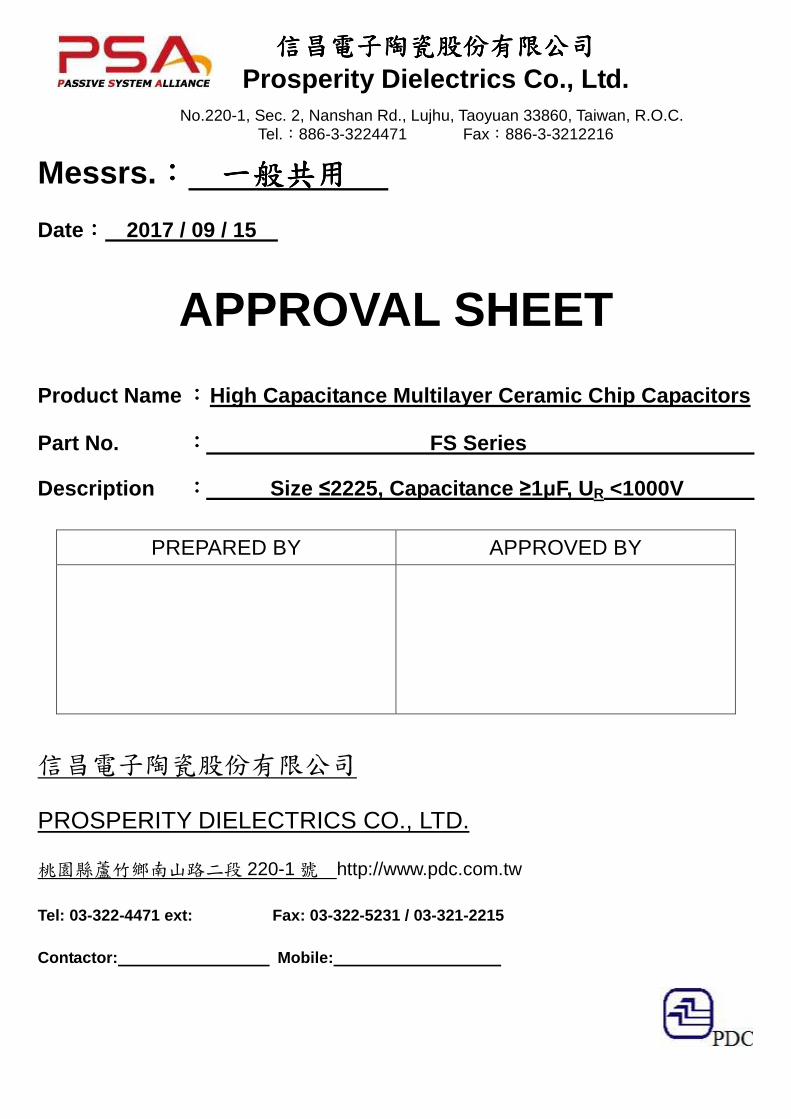
Messrs.:::: 一一一一般共用般共用般共用般共用 Date:::: 2017 / 09 / 15
APPROVAL SHEET
Product Name :::: High Capacitance Multilayer Ceramic Chip Capacitors
Part No. :::: FS Series
Description :::: Size ≤2225, Capacitance ≥1µF, UR <1000V
PREPARED BY APPROVED BY
信昌電子陶瓷股份有限公司
PROSPERITY DIELECTRICS CO., LTD.
桃園縣蘆竹鄉南山路二段 220-1號 http://www.pdc.com.tw
Tel: 03-322-4471 ext: Fax: 03-322-5231 / 0 3-321-2215
Contactor: Mobile:
信昌電子陶瓷股份有限公司信昌電子陶瓷股份有限公司信昌電子陶瓷股份有限公司信昌電子陶瓷股份有限公司 Prosperity Dielectrics Co., Ltd.
No.220-1, Sec. 2, Nanshan Rd., Lujhu, Taoyuan 33860, Taiwan, R.O.C. Tel.:886-3-3224471 Fax:886-3-3212216
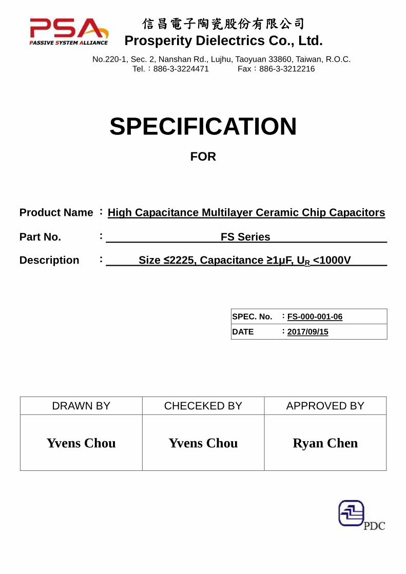
SPECIFICATION
FOR
Product Name :::: High Capacitance Multilayer Ceramic Chip Capacitors
Part No. :::: FS Series
Description :::: Size ≤2225, Capacitance ≥1µF, UR <1000V
SPEC. No. :::: FS-000-001-06
DATE :::: 2017/09/15
DRAWN BY CHECEKED BY APPROVED BY
Yvens Chou Yvens Chou Ryan Chen
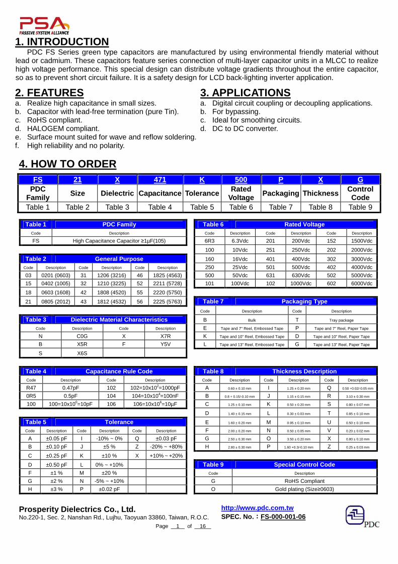
1. INTRODUCTION
PDC FS Series green type capacitors are manufactured by using environmental friendly material without lead or cadmium. These capacitors feature series connection of multi-layer capacitor units in a MLCC to realize high voltage performance. This special design can distribute voltage gradients throughout the entire capacitor, so as to prevent short circuit failure. It is a safety design for LCD back-lighting inverter application.
2. FEATURES a. Realize high capacitance in small sizes. b. Capacitor with lead-free termination (pure Tin). c. RoHS compliant. d. HALOGEM compliant. e. Surface mount suited for wave and reflow soldering. f. High reliability and no polarity.
3. APPLICATIONS a. Digital circuit coupling or decoupling applications. b. For bypassing. c. Ideal for smoothing circuits. d. DC to DC converter.
4. HOW TO ORDER
FS 21 X 471 K 500 P X G PDC
Family Size Dielectric Capacitance Tolerance Rated Voltage Packaging Thickness Control
Code Table 1 Table 2 Table 3 Table 4 Table 5 Table 6 Table 7 Table 8 Table 9
Table 1 PDC Family Table 6 Rated Voltage Code Description Code Description Code Description Code Description
FS High Capacitance Capacitor ≥1µF(105) 6R3 6.3Vdc 201 200Vdc 152 1500Vdc
100 10Vdc 251 250Vdc 202 2000Vdc
Table 2 General Purpose 160 16Vdc 401 400Vdc 302 3000Vdc
Code Description Code Description Code Description 250 25Vdc 501 500Vdc 402 4000Vdc
03 0201 (0603) 31 1206 (3216) 46 1825 (4563) 500 50Vdc 631 630Vdc 502 5000Vdc
15 0402 (1005) 32 1210 (3225) 52 2211 (5728) 101 100Vdc 102 1000Vdc 602 6000Vdc
18 0603 (1608) 42 1808 (4520) 55 2220 (5750)
21 0805 (2012) 43 1812 (4532) 56 2225 (5763) Table 7 Packaging Type
Code Description Code Description
Table 3 Dielectric Material Characteristics B Bulk T Tray package
Code Description Code Description E Tape and 7” Reel, Embossed Tape P Tape and 7” Reel, Paper Tape
N C0G X X7R K Tape and 10” Reel, Embossed Tape D Tape and 10” Reel, Paper Tape
B X5R F Y5V L Tape and 13” Reel, Embossed Tape G Tape and 13” Reel, Paper Tape
S X6S
Table 4 Capacitance Rule Code Table 8 Thickness Description Code Description Code Description Code Description Code Description Code Description
R47 0.47pF 102 102=10x102=1000pF A 0.60 ± 0.10 mm I 1.25 ± 0.20 mm Q 0.50 +0.02/-0.05 mm
0R5 0.5pF 104 104=10x104=100nF B 0.8 + 0.15/-0.10 mm J 1.15 ± 0.15 mm R 3.10 ± 0.30 mm
100 100=10x100=10pF 106 106=10x106=10µF C 1.25 ± 0.10 mm K 0.50 ± 0.20 mm S 0.80 ± 0.07 mm
D 1.40 ± 0.15 mm L 0.30 ± 0.03 mm T 0.85 ± 0.10 mm
Table 5 Tolerance E 1.60 ± 0.20 mm M 0.95 ± 0.10 mm U 0.50 ± 0.10 mm
Code Description Code Description Code Description F 2.00 ± 0.20 mm N 0.50 ± 0.05 mm V 0.20 ± 0.02 mm
A ±0.05 pF I -10% ~ 0% Q ±0.03 pF G 2.50 ± 0.30 mm O 3.50 ± 0.20 mm X 0.80 ± 0.10 mm
B ±0.10 pF J ±5 % Z -20% ~ +80% H 2.80 ± 0.30 mm P 1.60 +0.3/-0.10 mm Z 0.25 ± 0.03 mm
C ±0.25 pF K ±10 % X +10% ~ +20%
D ±0.50 pF L 0% ~ +10% Table 9 Special Control Code F ±1 % M ±20 % Code Description
G ±2 % N -5% ~ +10%
G RoHS Compliant
H ±3 % P ±0.02 pF O Gold plating (Size≥0603) http://www.pdc.com.tw Prosperity Dielectrics Co., Ltd.
No.220-1, Sec. 2, Nanshan Rd., Lujhu, Taoyuan 33860, Taiwan, R.O.C. SPEC. No.::::FS-000-001-06 Page 1 of 16
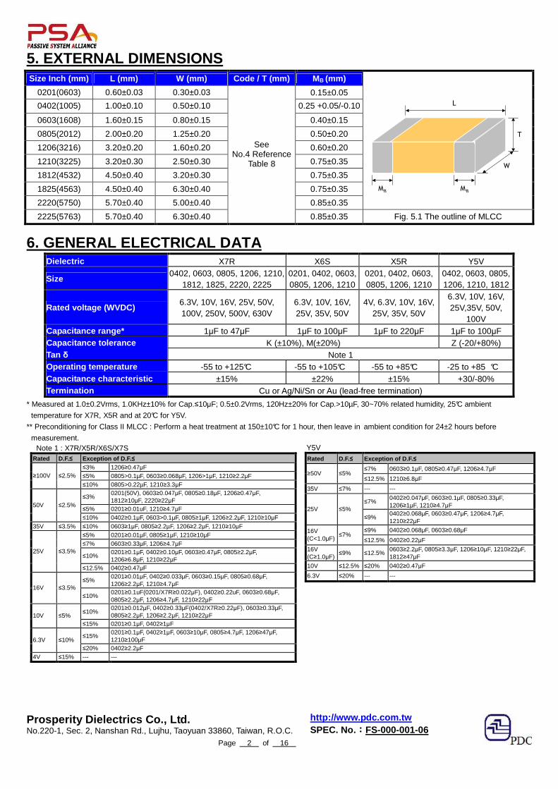
5. EXTERNAL DIMENSIONS Size Inch (mm) L (mm) W (mm) Code / T (mm) MB (mm)
0201(0603) 0.60±0.03 0.30±0.03 0.15±0.05
0402(1005) 1.00±0.10 0.50±0.10 0.25 +0.05/-0.10
0603(1608) 1.60±0.15 0.80±0.15 0.40±0.15
0805(2012) 2.00±0.20 1.25±0.20 0.50±0.20
1206(3216) 3.20±0.20 1.60±0.20 0.60±0.20
1210(3225) 3.20±0.30 2.50±0.30 0.75±0.35
1812(4532) 4.50±0.40 3.20±0.30 0.75±0.35
1825(4563) 4.50±0.40 6.30±0.40 0.75±0.35
2220(5750) 5.70±0.40 5.00±0.40 0.85±0.35
2225(5763) 5.70±0.40 6.30±0.40
See No.4 Reference
Table 8
0.85±0.35 Fig. 5.1 The outline of MLCC
6. GENERAL ELECTRICAL DATA Dielectric X7R X6S X5R Y5V
Size 0402, 0603, 0805, 1206, 1210,
1812, 1825, 2220, 2225 0201, 0402, 0603, 0805, 1206, 1210
0201, 0402, 0603, 0805, 1206, 1210
0402, 0603, 0805, 1206, 1210, 1812
Rated voltage (WVDC) 6.3V, 10V, 16V, 25V, 50V, 100V, 250V, 500V, 630V
6.3V, 10V, 16V, 25V, 35V, 50V
4V, 6.3V, 10V, 16V, 25V, 35V, 50V
6.3V, 10V, 16V, 25V,35V, 50V,
100V Capacitance range* 1µF to 47µF 1µF to 100µF 1µF to 220µF 1µF to 100µF Capacitance tolerance K (±10%), M(±20%) Z (-20/+80%) Tan δ Note 1 Operating temperature -55 to +125°C -55 to +105°C -55 to +85°C -25 to +85 °C Capacitance characteristic ±15% ±22% ±15% +30/-80% Termination Cu or Ag/Ni/Sn or Au (lead-free termination)
* Measured at 1.0±0.2Vrms, 1.0KHz±10% for Cap.≤10µF; 0.5±0.2Vrms, 120Hz±20% for Cap.>10µF, 30~70% related humidity, 25°C ambient
temperature for X7R, X5R and at 20°C for Y5V.
** Preconditioning for Class II MLCC : Perform a heat treatment at 150±10°C for 1 hour, then leave in ambient condition for 24±2 hours before
measurement.
http://www.pdc.com.tw Prosperity Dielectrics Co., Ltd. No.220-1, Sec. 2, Nanshan Rd., Lujhu, Taoyuan 33860, Taiwan, R.O.C. SPEC. No.::::FS-000-001-06
Page 2 of 16
T
W
L
MB
MB
Note 1 : X7R/X5R/X6S/X7S Rated D.F.≤ Exception of D.F. ≤
≤3% 1206≥0.47µF ≤5% 0805>0.1µF, 0603≥0.068µF, 1206>1µF, 1210≥2.2µF ≥100V ≤2.5%
≤10% 0805>0.22µF, 1210≥3.3µF
≤3% 0201(50V), 0603≥0.047µF, 0805≥0.18µF, 1206≥0.47µF, 1812≥10µF, 2220≥22µF
≤5% 0201≥0.01uF, 1210≥4.7µF 50V ≤2.5%
≤10% 0402≥0.1µF, 0603>0.1µF, 0805≥1µF, 1206≥2.2µF, 1210≥10µF 35V ≤3.5% ≤10% 0603≥1µF, 0805≥2.2µF, 1206≥2.2µF, 1210≥10µF
≤5% 0201≥0.01µF, 0805≥1µF, 1210≥10µF ≤7% 0603≥0.33µF, 1206≥4.7µF
≤10% 0201≥0.1µF, 0402≥0.10µF, 0603≥0.47µF, 0805≥2.2µF, 1206≥6.8µF, 1210≥22µF
25V ≤3.5%
≤12.5% 0402≥0.47µF
≤5% 0201≥0.01µF, 0402≥0.033µF, 0603≥0.15µF, 0805≥0.68µF, 1206≥2.2µF, 1210≥4.7µF
16V ≤3.5% ≤10%
0201≥0.1uF(0201/X7R≥0.022µF), 0402≥0.22uF, 0603≥0.68µF, 0805≥2.2µF, 1206≥4.7µF, 1210≥22µF
≤10% 0201≥0.012µF, 0402≥0.33µF(0402/X7R≥0.22µF), 0603≥0.33µF, 0805≥2.2µF, 1206≥2.2µF, 1210≥22µF 10V ≤5%
≤15% 0201≥0.1µF, 0402≥1µF
≤15% 0201≥0.1µF, 0402≥1µF, 0603≥10µF, 0805≥4.7µF, 1206≥47µF, 1210≥100µF 6.3V ≤10%
≤20% 0402≥2.2µF 4V ≤15% --- ---
Y5V Rated D.F.≤ Exception of D.F. ≤
≤7% 0603≥0.1µF, 0805≥0.47µF, 1206≥4.7µF ≥50V ≤5%
≤12.5% 1210≥6.8µF
35V ≤7% --- ---
≤7% 0402≥0.047µF, 0603≥0.1µF, 0805≥0.33µF, 1206≥1µF, 1210≥4.7µF
25V ≤5% ≤9%
0402≥0.068µF, 0603≥0.47µF, 1206≥4.7µF, 1210≥22µF
≤9% 0402≥0.068µF, 0603≥0.68µF 16V (C<1.0µF)
≤7% ≤12.5% 0402≥0.22µF
16V (C≥1.0µF)
≤9% ≤12.5% 0603≥2.2µF, 0805≥3.3µF, 1206≥10µF, 1210≥22µF, 1812≥47µF
10V ≤12.5% ≤20% 0402≥0.47µF
6.3V ≤20% --- ---
7. CAPACITANCE RANGE 7-1. X7R
Dimension 0402 0603 0805 1206 Cap(pF) code 16V 6.3V 10V 16V 25V 50V 6.3V 10V 16V 25V 50V 6.3V 10V 16V 25V 50V 100V 1000000 105 N B B B B B C C C I J J J P P 1200000 125 P P P 1500000 155 I I I J J J P P 1800000 185 P P 2200000 225 B B B I I I I I J J J P P P 2700000 275 3300000 335 P P P P 3900000 395 4700000 475 B I I I I P P P P P 5600000 565 6800000 685 8200000 825
10000000 106 I I I* P P P P 12000000 126 15000000 156 18000000 186 22000000 226 P P P* 47000000 476
Dimension 1210 1812 1825 Cap(pF) code 6.3V 10V 16V 25V 50V 100V 10V 16V 25V 50V 100V 200V 250V 25V 50V 100V 200V 250V 1000000 105 C C C C F C C C F F G G G F F F F 1200000 125 G G C F F F F G G 1500000 155 E E G G C F F F F G G 1800000 185 G G E F F F F G G 2200000 225 E E G G E F G F F G G 2700000 275 G G F F G F F H H 3300000 335 E E G G F F G F F 3900000 395 F F G F F 4700000 475 F F F G G G G G F G 5600000 565 G G G G G 6800000 685 G G G G 8200000 825 G G G G
10000000 106 F F F G G G G G 12000000 126 15000000 156 18000000 186 22000000 226 G G G 47000000 476 G G
Dimension 2220 2225 Cap(pF) code 25V 50V 100V 200V 250V 500V 630V 25V 50V 100V 200V 250V 500V 630V 1000000 105 F F F F F H H F F F F F G G 1200000 125 F F F G G F F F G G H H 1500000 155 F F F G G F F F G G H H 1800000 185 F F F G G F F F G G 2200000 225 F F F G G F F F G G 2700000 275 F F F H H F F F G G 3300000 335 F F F F F F H H 3900000 395 F F F F F F H H 4700000 475 F F F F F G 5600000 565 F F F F F G 6800000 685 F F F F F G 8200000 825 G G G G G G
10000000 106 G G G G G G 12000000 126 H H 15000000 156 H H 18000000 186 H H 22000000 226 H H H H 47000000 476
http://www.pdc.com.tw Prosperity Dielectrics Co., Ltd. No.220-1, Sec. 2, Nanshan Rd., Lujhu, Taoyuan 33860, Taiwan, R.O.C. SPEC. No.::::FS-000-001-06
Page 3 of 16
7. CAPACITANCE RANGE(Con.) 7-2. X5R
Dimension 0201 0402 0603 Cap(pF) code 6.3V 10V 16V 4V 6.3V 10V 16V 25V 4V 6.3V 10V 16V 25V 50V 1000000 105 L L L N N N N B B B B B 1500000 155 B 2200000 225 L N N K K B B B B B 3300000 335 B B 4700000 475 K K K B B B B 6800000 685
10000000 106 K K K B B B B B 22000000 226 B B B 47000000 476 B B 100000000 107 220000000 227
Dimension 0805 1206
Cap(pF) code 4V 6.3V 10V 16V 25V 50V 4V 6.3V 10V 16V 25V 50V 1000000 105 C C C I P 1500000 155 I I I I J J 2200000 225 I I I I I J J P P 3300000 335 I I I I P P P 4700000 475 I I I I I P P P P P 6800000 685 P P
10000000 106 I I I I I P P P P P 22000000 226 I I I I P P P P 47000000 476 I I P P P 100000000 107 I I P 220000000 227 P
Dimension 1210
Cap(pF) code 4V 6.3V 10V 16V 25V 35V 50V 1000000 105 1500000 155 F F 2200000 225 F F 3300000 335 4700000 475 F F F 6800000 685
10000000 106 F F F F G G 22000000 226 G G G G G 47000000 476 G G G G 100000000 107 G G G 220000000 227 G G
http://www.pdc.com.tw Prosperity Dielectrics Co., Ltd. No.220-1, Sec. 2, Nanshan Rd., Lujhu, Taoyuan 33860, Taiwan, R.O.C. SPEC. No.::::FS-000-001-06
Page 4 of 16
7. CAPACITANCE RANGE(Con.) 7-3. Y5V
Dimension 0402 0603 0805 1206 Cap(pF) code 6.3V 10V 6.3V 10V 16V 25V 6.3V 10V 16V 25V 50V 6.3V 10V 16V 25V 35V 50V 1000000 105 N N S B B X X C C M M M M 1500000 155 S C C M M M 2200000 225 S S B C C I I M M M J 3300000 335 C C J J J 4700000 475 B B C C I J J J J P 6800000 685 I J J
10000000 106 I I I J J P 22000000 226 I I P P 47000000 476 P 100000000 107 220000000 227
Dimension 1210 1812
Cap(pF) code 6.3V 10V 16V 25V 35V 50V 10V 16V 25V 50V 100V 1000000 105 M M M M C C C C C 1500000 155 M M M C C C C 2200000 225 M M M E C C C C 3300000 335 M M M C C C C 4700000 475 M M C E C C C C 6800000 685 M M C F C C C C
10000000 106 C C E F F C C C F 22000000 226 F F 47000000 476 F F G 100000000 107 G 220000000 227
7-4. X6S
Dimension 0201 0402 0603 0805 Cap(pF) code 4V 6.3V 6.3V 10V 16V 25V 4V 6.3V 10V 16V 25V 4V 6.3V 10V 16V 25V 50V 1000000 105 L L* K K K K 1500000 155 2200000 225 K K K B B 3300000 335 4700000 475 K* B B B I I 6800000 685
10000000 106 K* B* B* B* I I I I I 22000000 226 B* B* I* I* I* 47000000 476 I* I* 100000000 107 I* 220000000 227
Dimension 1206 1210 Cap(pF) code 6.3V 10V 16V 25V 6.3V 10V 16V 25V 1000000 105 1500000 155 2200000 225 3300000 335 4700000 475 6800000 685
10000000 106 P 22000000 226 P P* P G 47000000 476 p G G G 100000000 107 G* G* 220000000 227
“*” Means M tolerance only.
http://www.pdc.com.tw Prosperity Dielectrics Co., Ltd. No.220-1, Sec. 2, Nanshan Rd., Lujhu, Taoyuan 33860, Taiwan, R.O.C. SPEC. No.::::FS-000-001-06
Page 5 of 16
8. RELIABILITY TEST CONDITIONS AND REQUIREMENTS
No. Item Test Condition Requirements
1. Visual and Dimensions
--- * No remarkable defect. * Dimensions to confirm to individual specification sheet.
2. Capacitance * Shall not exceed the limits given in the detailed spec.
3.
Q/D.F.
(Dissipation
Factor)
* Class II : (X7R, X6S, X5R, Y5V)
Cap.≤10µF, 1.0±0.2Vrms, 1KHz±10%**.
Cap.>10µF, 0.5±0.2Vrms, 120Hz±20%.
** Test condition : 0.5±0.2Vrms, 1KHz±10%.
X7R :
0805=106(6.3V&10V), 0603=475(6.3V).
X6S :
0201≥104(6.3V&10V),0402≥225(6.3V),
0402/475(10V), 0603/106(6.3V).
X5R :
01R5≥103, 0201≥224(6.3V,10V,16V)#1,
0402≥475(6.3V,16V), 0402≥225(10V),
0603=106(6.3V,10V).
X7R, X5R, X6S Rated D.F.≤ Exception of D.F.≤
≤3% 1206≥0.47µF ≤5% 0805>0.1µF, 0603≥0.068µF, 1206>1µF, 1210≥2.2µF ≥100V ≤2.5%
≤10% 0805>0.22µF, 1210≥3.3µF
≤3% 0201(50V), 0603≥0.047µF, 0805≥0.18µF, 1206≥0.47µF, 1812≥10µF, 2220≥22µF
≤5% 0201≥0.01uF, 1210≥4.7µF 50V ≤2.5%
≤10% 0402≥0.1µF, 0603>0.1µF, 0805≥1µF, 1206≥2.2µF, 1210≥10µF
35V ≤3.5% ≤10% 0603≥1µF, 0805≥2.2µF, 1206≥2.2µF, 1210≥10µF ≤5% 0201≥0.01µF, 0805≥1µF, 1210≥10µF ≤7% 0603≥0.33µF, 1206≥4.7µF
≤10% 0201≥0.1µF, 0402≥0.10µF, 0603≥0.47µF, 0805≥2.2µF, 1206≥6.8µF, 1210≥22µF
25V ≤3.5%
≤12.5% 0402≥0.47µF
≤5% 0201≥0.01µF, 0402≥0.033µF, 0603≥0.15µF, 0805≥0.68µF, 1206≥2.2µF, 1210≥4.7µF
16V ≤3.5% ≤10%
0201≥0.1uF(0201/X7R≥0.022µF), 0402≥0.22uF, 0603≥0.68µF, 0805≥2.2µF, 1206≥4.7µF, 1210≥22µF
≤10% 0201≥0.012µF, 0402≥0.33µF(0402/X7R≥0.22µF), 0603≥0.33µF, 0805≥2.2µF, 1206≥2.2µF, 1210≥22µF 10V ≤5%
≤15% 0201≥0.1µF, 0402≥1µF
≤15% 0201≥0.1µF, 0402≥1µF, 0603≥10µF, 0805≥4.7µF, 1206≥47µF, 1210≥100µF 6.3V ≤10%
≤20% 0402≥2.2µF 4V ≤15% --- ---
Y5V Rated Vol. D.F.≤ Exception of D.F.≤
≤7% 0603≥0.1µF, 0805≥0.47µF, 1206≥4.7µF ≥50V ≤5%
≤12.5% 1210≥6.8µF 35V ≤7% --- ---
≤7% 0402≥0.047µF, 0603≥0.1µF, 0805≥0.33µF, 1206≥1µF, 1210≥4.7µF
25V ≤5% ≤9%
0402≥0.068µF, 0603≥0.47µF, 1206≥4.7µF, 1210≥22µF
≤9% 0402≥0.068µF, 0603≥0.68µF 16V (C<1.0µF)
≤7% ≤12.5% 0402≥0.22µF
16V (C≥1.0µF)
≤9% ≤12.5% 0603≥2.2µF, 0805≥3.3µF, 1206≥10µF, 1210≥22µF, 1812≥47µF
10V ≤12.5% ≤20% 0402≥0.47µF 6.3V ≤20% --- ---
4. Temperature
Coefficient
* With no electrical load. T.C. Operating Temp. X7R -55~125°C at 25°C X6S -55~105°C at 25°C X5R -55~ 85°C at 25°C Y5V -25~ 85°C at 20°C
* Measurement voltage for Class II : Size Cap. Range Condition
Cap.<0.1µF 1V 0.1µF≤Cap.<1µF 0.2V 0201
Cap.≥1µF 0.1V Cap.<0.1µF 1V Cap.=1µF 0.5V
1µF<Cap.<10µF 0.2V 0402
Cap.≥10µF 0.1V Cap.≤1µF 1V
1µF<Cap.≤4.7µF 0.5V 0603
Cap.>4.7µF 0.2V Cap.<10µF 1V Cap.=10µF 0.5V 0805
Cap.>10µF 0.2V Cap.≤10µF 1V
10µF<Cap.≤100µF 0.5V 1206/1210
Cap.>100µF 0.2V
T.C. Capacitance Change
X7R Within ±15%
X6S Within ±22%
X5R Within ±15%
Y5V Within +30%/-80%
http://www.pdc.com.tw Prosperity Dielectrics Co., Ltd.
No.220-1, Sec. 2, Nanshan Rd., Lujhu, Taoyuan 33860, Taiwan, R.O.C. SPEC. No.::::FS-000-001-06 Page 6 of 16
8. RELIABILITY TEST CONDITIONS AND REQUIREMENTS
No. Item Test Condition Requirements
5. Insulation
Resistance
* To apply rated voltage for Max. 120sec.
* Before initial measurement (Class II only) : To apply
de-aging at 150°C for 1hr then set for 24±2 hrs at
room temp.
* ≥10GΩ or RxC≥500Ω-F, whichever is smaller.
* Class II (X7R, X5R, X6S, Y5V) : Rated voltage I.R. 100V : All X7R 50V : 0402>0.01µF, 0603≥1µF, 0805≥1µF, 1206≥4.7µF, 1210≥4.7µF 35V : 0805≥2.2µF, 1206≥2.2µF, 1210≥10µF 25V : 0402≥1µF, 0603≥2.2µF, 0805≥2.2µF, 1206≥10µF, 1210≥10µF 16V : 0201≥0.1µF, 0402≥0.22µF, 0603≥1µF, 0805≥2.2µF, 1206≥10µF, 1210≥47µF 10V : 0201≥47nF, 0402≥0.47µF, 0603≥0.47µF, 0805≥2.2µF, 1206≥4.7µF, 1210≥47µF 6.3V, 4V
≥10GΩ or RxC≥100Ω-F, whichever is smaller
Rated voltage I.R. 100V : 1210≥3.3µF 50V : 0402≥0.1µF, 0603≥2.2µF, 0805≥10µF, 1206≥10µF 35V : 0603≥1µF 25V : 0201≥0.1µF, 0402≥2.2µF, 0603≥10µF, 0805≥10µF, 1206≥22µF 16V : 0603≥10µF, 0402≥1µF, 0201≥0.22µF 10V : 0201>0.1µF, 0402≥1µF, 0603≥10µF, 0805≥47µF 6.3V : 0201≥0.1µF, 0603>4.7µF, 0805≥47µF, 1206≥10µF 4V : 0603≥22µF, 0805≥47µF, 1206≥100µF
RxC≥50Ω-F
6. Dielectric
Strength
Rated Voltage Condition
≤100 2.5 times of UR
100<V≤250 2.0 times of UR
250<V≤500 1.5 times of UR
630 1.2 times of UR
* Duration : 1 to 5 sec.
* Charge and discharge current less than 50mA.
* No evidence of damage or flash over during test.
7. Solderability * Solder temperature : 235±5°C for (0201~1210).
* Solder temperature : 245±5°C for (1808~2225).
* Dipping time : 2±0.5 sec.
* 75% min. coverage of all metalized area.
8. Resistance
to Soldering
Heat
* Solder temperature : 260±5°C.
* Dipping time : 10±1 sec.
* Preheating : 120 to 150°C for 1 minute before
immerse the capacitor in a eutectic solder.
* Before initial measurement (Class II only) : To apply
de-aging at 150°C for 1hr then set for 24±2 hrs at
room temp.
* Cap. / D.F. / I.R. Measurement to be made after
de-aging at 150°C for 1hr then set for 24±2 hrs at
room temp.
* No remarkable damage.
* Cap. change :
X7R, X5R, X6S : Within ±7.5%.
Y5V : Within ±20%.
* D.F., I.R. and dielectric strength : To meet initial requirements.
* 25% max. leaching on each edge.
9. Temperature
Cycle
* Conduct the five cycles according to the
temperatures and time. Step Temp.(°C) Time(min.)
1 Min. operating temp. +0/-3 30±3
2 Room temp. 2~3
3 Max. operating temp. +3/-0 30±3
4 Room temp. 2~3
* Before initial measurement (Class II only) : To apply
de-aging at 150°C for 1hr then set for 24±2 hrs at
room temp.
* Cap./D.F./I.R. measurement to made after de-aging
at 150°C for 1hr then set for 24±2 hrs at room temp .
* No remarkable damage.
* Cap. change :
X7R, X5R, X6S : Within ±7.5%.
Y5V : Within ±20%.
* D.F. : ≤150% of initial requirement.
* I.R. : ≥25% of initial requirement.
http://www.pdc.com.tw Prosperity Dielectrics Co., Ltd.
No.220-1, Sec. 2, Nanshan Rd., Lujhu, Taoyuan 33860, Taiwan, R.O.C. SPEC. No.::::FS-000-001-06 Page 7 of 16
8. RELIABILITY TEST CONDITIONS AND REQUIREMENTS
No. Item Test Condition Requirements
10. Humidity
(Damp Heat)
Steady State
* Test temp. : 40±2°C.
* Humidity : 90~95%RH.
* Test time : 500 +24/-0hrs.
* Measurement to be made after keeping at room
temp. for 48±4 hrs (Class II).
* No remarkable damage.
* Cap. change :
X7R, X5R, X6S : Within ±12.5% for ≥10V**, within ±25% for 6.3V.
**10V : Within ±25% for 0603≥4.7µF, 0402≥1µF, 0201≥0.1µF.
Y5V : Within ±30% for ≥10V, within +30/-40% for 6.3V.
* D.F.(Class II) : ≤200% of initial requirement.
* I.R. : ≥10V, ≥1GΩ or R×C≥50Ω-F, whichever is smaller.
6.3V, R×C≥10Ω-F.
11.
Humidity
(Damp Heat)
Load
* Test temp. : 40±2°C.
* Humidity : 90~95%RH.
* Test time : 500 +24/-0hrs.
* To apply voltage : Rated voltage (500V max.).
* Measurement to be made after keeping at room
temp. for 48±4 hrs (Class II).
* No remarkable damage.
* Cap. change :
X7R, X5R, X6S : Within ±12.5% for ≥10V**, within ±25% for 6.3V.
**10V : Within ±25% for 0603≥4.7µF, 0402≥1µF, 0201≥0.1µF.
Y5V : Within ±30% for ≥10V, within +30/-40% for 6.3V.
* D.F.(Class II) : ≤200% of initial requirement.
* I.R. : ≥10V, ≥500MΩ or RxC≥25Ω-F, whichever is smaller.
Class II (X7R, X5R, X6S, Y5V) Rated voltage I.R. 100V : All X7R, 1210≥3.3µF 50V : 0402>0.01µF, 0603≥1µF, 0805≥1µF, 1206≥4.7µF, 1210≥4.7µF 35V : 0603≥1µF, 0805≥2.2µF, 1206≥2.2µF, 1210≥10µF 25V : 0201≥0.1uF, 0402≥0.22µF, 0603≥2.2µF, 0805≥2.2µF, 1206≥10µF,
1210≥10µF 16V : 0201≥0.1uF, 0402≥0.22µF, 0603≥1µF, 0805≥2.2µF, 1206≥10µF,
1210≥47µF 10V : 0201≥47nF, 0402≥0.47µF, 0603≥0.47µF, 0805≥2.2µF, 1206≥4.7µF, 1210≥47µF 6.3V, 4V, All X6S/X7S items, Size≥1812
≥500MΩ or RxC≥5Ω-F, whichever is smaller
http://www.pdc.com.tw Prosperity Dielectrics Co., Ltd. No.220-1, Sec. 2, Nanshan Rd., Lujhu, Taoyuan 33860, Taiwan, R.O.C. SPEC. No.::::FS-000-001-06
Page 8 of 16
8. RELIABILITY TEST CONDITIONS AND REQUIREMENTS No. Item Test Condition Requirements
12. High
Temperature
Load
(Endurance)
* Test temp. :
X7R : 125±3°C.
X6S : 105±3°C.
X5R, Y5V : 85±3°C.
* To apply voltage :
(1) ≤6.3V or Cap.≥10µF : 150% of rated voltage.
(2) 10V≤Ur<500V : 200% of rated voltage.
(3) 500V : 150% of rated voltage.
(4) Ur≥630V : 120% of rated voltage.
(5) 100% of rated voltage for below range : Size Dielectric Rated Capacitance range
≤10V C≥0.1µF 0201 X5R/X7R/X6S ≥16V C>0.1µF
0402 X5R/X7R/X6S /Y5V
6.3V, 10V, 16V, 25V
C≥1.0µF
4V C≥22µF 6.3V,10V C≥4.7µF 0603 X5R/X7R/X6S 25V, 35V C≥1.0µF 4V C≥47µF 6.3V C≥22µF 0805 X5R/X7R/X6S 10V~50V C≥10µF
1206 X5R/X7R/X6S ≤6.3V C≥47µF X5R/X7R/X6S 16V C≥47µF 1210 X7R 100V C≥3.3µF
(6) 150% of rated voltage for below range : Size Dielectric Rated Voltage Capacitance
X5R/X7R/X6S 16V/25V C≥0.1µF 0201 X7R 16V C≥0.022µF
50V C≥0.1µF X5R/X7R/X6S 10~25V C≥0.22µF 0402
Y5V 16V C≥0.47µF X7R 50V C>0.1µF X5R/X7R/X6S 10V,16V, 50V C≥1.0µF 0603 Y5V 16V C≥2.2µF X5R/X7R/X6S 10~50V C≥4.7µF
50V C≥2.2µF X5R/X7R/X6S 100V C≥0.12µF
0805
Y5V 16V C≥4.7µF 1206 X5R/X7R/X6S 50V~100V C>1.0µF
X5R/X7R/X6S 50V~100V C≥1.0µF 1210 X7R 200V~250V C≥0.22µF
100V C≥1.0µF 1812 X7R 200V~250V C≥0.47µF
1825 2220 2225
X7R 100V~250V C≥1.0µF
(7) 120% of rated voltage for below range : Size Dielectric Rated Voltage Capacitance 1210 X7R 100V C≥3.3µF
* Test time : 1000 +24/-0 hrs.
* Before initial measurement (Class II only) : To apply
de-aging at 150°C for 1hr then set for 24±2 hrs at
room temp.
* Cap./D.F./I.R. measurement to be made after de-aging at
150°C for 1hr then set for 24±2 hrs at room temp.
** De-rating conditions :
* No remarkable damage.
* Cap. change :
X7R, X5R, X6S : Within ±12.5% for ≥10V**, within ±25% for ≤6.3V.
**10V : Within ±25% for 0603≥4.7µF, 0402≥1µF, 0201≥0.1µF.
Y5V : Within ±30% for ≥10V, within +30/-40% for ≤6.3V.
* D.F.(Class II) : ≤200% of initial requirement.
* I.R. : ≥10V, ≥1GΩ or RxC≥50Ω-F, whichever is smaller.
Class II (X7R, X5R, X6S, Y5V) Rated voltage I.R. 100V : All X7R, 1210≥3.3µF 50V : 0402>0.01µF, 0603≥1µF, 0805≥1µF, 1206≥4.7µF, 1210≥4.7µF 35V : 0603≥1µF, 0805≥2.2µF, 1206≥2.2µF, 1210≥10µF 25V : 0201≥0.1uF, 0402≥0.22µF, 0603≥2.2µF, 0805≥2.2µF, 1206≥10µF,
1210≥10µF 16V : 0201≥0.1uF, 0402≥0.22µF, 0603≥1µF, 0805≥2.2µF, 1206≥10µF,
1210≥47µF 10V : 0201≥47nF, 0402≥0.47µF, 0603≥0.47µF, 0805≥2.2µF, 1206≥4.7µF, 1210≥47µF 6.3V, 4V, All X6S/X7S items, Size≥1812
≥1GΩ or RxC≥10Ω-F, whichever is smaller
http://www.pdc.com.tw Prosperity Dielectrics Co., Ltd.
No.220-1, Sec. 2, Nanshan Rd., Lujhu, Taoyuan 33860, Taiwan, R.O.C. SPEC. No.::::FS-000-001-06
Page 9 of 16
8. RELIABILITY TEST CONDITIONS AND REQUIREMENTS No. Item Test Condition Requirements
13.
Adhesive
Strength of
Termination
* Capacitors mounted on a substrate. A force of
5N(≤0603) or 10N(>0603) applied perpendicular to
the place of substrate and parallel the line joining
the center of terminations for 10±1 second.
* No remarkable damage or removal of the terminations.
14. Bending Test
* The middle part of substrate shall be pressurized by
means of the pressurizing rod at a rate of about 1mm
per second until the deflection becomes 1mm.
Unit : mm
* No remarkable damage.
Dielectric Cap. Change
Class II (X7R, X5R, X6S) Within ±12.5%
Class II (Y5V) Within ±30%
(This capacitance change means the change of capacitance under
specified flexure of substrate from the capacitance measured before the
test)
15. Vibration
Resistance
* Vibration frequency : 10~55 Hz/min.
* Total amplitude : 1.5mm.
* Test time : 6 hrs. (Two hrs each in three mutually
perpendicular directions)
* No remarkable damage.
* Cap. change and D.F. : To meet initial spec.
http://www.pdc.com.tw Prosperity Dielectrics Co., Ltd. No.220-1, Sec. 2, Nanshan Rd., Lujhu, Taoyuan 33860, Taiwan, R.O.C. SPEC. No.::::FS-000-001-06
Page 10 of 16
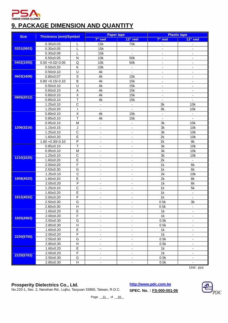
9. PACKAGE DIMENSION AND QUANTITY
Paper tape Plastic tape Size Thickness (mm)/Symbol 7” reel 13” reel 7” reel 13” reel
0.30±0.03 L 15k 70k - - 0.30±0.05 L 15k - - - 0201(0603) 0.30±0.09 L 15k - - - 0.50±0.05 N 10k 50k - -
0.50 +0.02/-0.05 Q 10k 50k - - 0402(1005) 0.50±0.20 K 10k - - - 0.50±0.10 U 4k - - - 0.80±0.07 S 4k 15k - - 0603(1608)
0.80 +0.15/-0.10 B 4k 15k - - 0.50±0.10 U 4k 15k - - 0.60±0.10 A 4k 15k - - 0.80±0.10 X 4k 15k - - 0.85±0.10 T 4k 15k - - 1.25±0.10 C - - 3k 10k
0805(2012)
1.25±0.20 I - - 3k 10k 0.80±0.10 X 4k 15k - - 0.85±0.10 T 4k 15k - - 0.95±0.10 M - - 3k 10k 1.15±0.15 J - - 3k 10k 1.25±0.10 C - - 3k 10k 1.60±0.20 E - - 2k 10k
1206(3216)
1.60 +0.30/-0.10 P - - 2k 9k 0.85±0.10 T - - 3k 10k 0.95±0.10 M - - 3k 10k 1.25±0.10 C - - 3k 10k 1.60±0.20 E - - 2k - 2.00±0.20 F - - 1k 6k
1210(3225)
2.50±0.30 G - - 1k 6k 1.25±0.10 C - - 2k 10k 1.60±0.20 E - - 2k 8k 1808(4520) 2.00±0.20 F - - 1k 6k 1.25±0.10 C - - 1k 5k 1.60±0.20 E - - 1k - 2.00±0.20 F - - 1k - 2.50±0.30 G - - 0.5k 3k
1812(4532)
2.80±0.30 H - - 0.5k - 1.60±0.20 E - - 1k - 2.00±0.20 F - - 1k - 2.50±0.30 G - - 0.5k -
1825(4563)
2.80±0.30 H - - 0.5k - 1.60±0.20 E - - 1k - 2.00±0.20 F - - 1k - 2.50±0.30 G - - 0.5k -
2220(5750)
2.80±0.30 H - - 0.5k - 1.60±0.20 E - - 1k - 2.00±0.20 F - - 1k - 2.50±0.30 G - - 0.5k -
2225(5763)
2.80±0.30 H - - 0.5k -
Unit : pcs
http://www.pdc.com.tw Prosperity Dielectrics Co., Ltd. No.220-1, Sec. 2, Nanshan Rd., Lujhu, Taoyuan 33860, Taiwan, R.O.C. SPEC. No.::::FS-000-001-06
Page 11 of 16
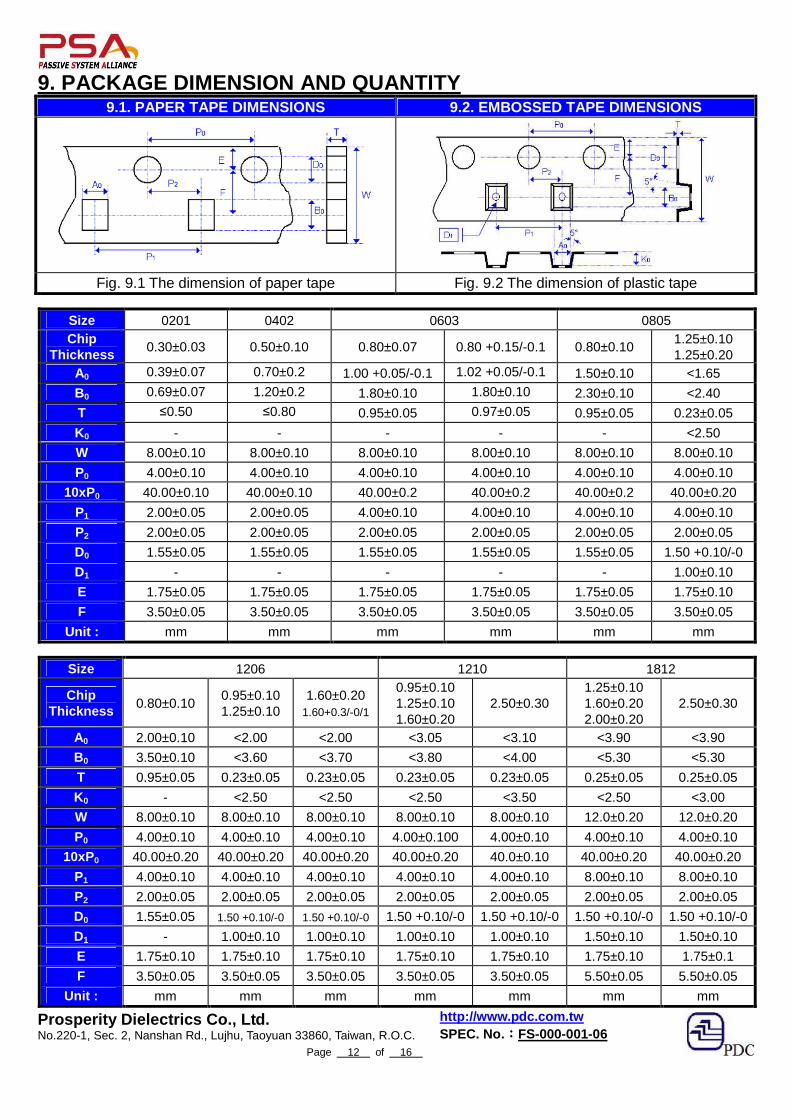
9. PACKAGE DIMENSION AND QUANTITY
9.1. PAPER TAPE DIMENSIONS 9.2. EMBOSSED TAPE DIMENSIONS
Fig. 9.1 The dimension of paper tape Fig. 9.2 The dimension of plastic tape
Size 0201 0402 0603 0805 Chip
Thickness 0.30±0.03 0.50±0.10 0.80±0.07 0.80 +0.15/-0.1 0.80±0.10 1.25±0.10 1.25±0.20
A0 0.39±0.07 0.70±0.2 1.00 +0.05/-0.1 1.02 +0.05/-0.1 1.50±0.10 <1.65
B0 0.69±0.07 1.20±0.2 1.80±0.10 1.80±0.10 2.30±0.10 <2.40
T ≤0.50 ≤0.80 0.95±0.05 0.97±0.05 0.95±0.05 0.23±0.05
K0 - - - - - <2.50
W 8.00±0.10 8.00±0.10 8.00±0.10 8.00±0.10 8.00±0.10 8 .00±0.10
P0 4.00±0.10 4.00±0.10 4.00±0.10 4.00±0.10 4.00±0.10 4 .00±0.10
10xP0 40.00±0.10 40.00±0.10 40.00±0.2 40.00±0.2 40.00±0.2 40.00±0.20
P1 2.00±0.05 2.00±0.05 4.00±0.10 4.00±0.10 4.00±0.10 4 .00±0.10
P2 2.00±0.05 2.00±0.05 2.00±0.05 2.00±0.05 2.00±0.05 2 .00±0.05
D0 1.55±0.05 1.55±0.05 1.55±0.05 1.55±0.05 1.55±0.05 1 .50 +0.10/-0
D1 - - - - - 1.00±0.10
E 1.75±0.05 1.75±0.05 1.75±0.05 1.75±0.05 1.75±0.05 1 .75±0.10
F 3.50±0.05 3.50±0.05 3.50±0.05 3.50±0.05 3.50±0.05 3 .50±0.05
Unit : mm mm mm mm mm mm
Size 1206 1210 1812
Chip Thickness 0.80±0.10
0.95±0.10 1.25±0.10
1.60±0.20 1.60+0.3/-0/1
0.95±0.10 1.25±0.10 1.60±0.20
2.50±0.30 1.25±0.10 1.60±0.20 2.00±0.20
2.50±0.30
A0 2.00±0.10 <2.00 <2.00 <3.05 <3.10 <3.90 <3.90
B0 3.50±0.10 <3.60 <3.70 <3.80 <4.00 <5.30 <5.30
T 0.95±0.05 0.23±0.05 0.23±0.05 0.23±0.05 0.23±0.05 0 .25±0.05 0.25±0.05
K0 - <2.50 <2.50 <2.50 <3.50 <2.50 <3.00
W 8.00±0.10 8.00±0.10 8.00±0.10 8.00±0.10 8.00±0.10 1 2.0±0.20 12.0±0.20
P0 4.00±0.10 4.00±0.10 4.00±0.10 4.00±0.100 4.00±0.10 4.00±0.10 4.00±0.10
10xP0 40.00±0.20 40.00±0.20 40.00±0.20 40.00±0.20 40.0±0.10 40.00±0.20 40.00±0.20
P1 4.00±0.10 4.00±0.10 4.00±0.10 4.00±0.10 4.00±0.10 8 .00±0.10 8.00±0.10
P2 2.00±0.05 2.00±0.05 2.00±0.05 2.00±0.05 2.00±0.05 2 .00±0.05 2.00±0.05
D0 1.55±0.05 1.50 +0.10/-0 1.50 +0.10/-0 1.50 +0.10/-0 1.50 +0.10/-0 1.50 +0.10/-0 1.50 +0.10/-0
D1 - 1.00±0.10 1.00±0.10 1.00±0.10 1.00±0.10 1.50±0.10 1.50±0.10
E 1.75±0.10 1.75±0.10 1.75±0.10 1.75±0.10 1.75±0.10 1 .75±0.10 1.75±0.1
F 3.50±0.05 3.50±0.05 3.50±0.05 3.50±0.05 3.50±0.05 5 .50±0.05 5.50±0.05 Unit : mm mm mm mm mm mm mm
http://www.pdc.com.tw Prosperity Dielectrics Co., Ltd. No.220-1, Sec. 2, Nanshan Rd., Lujhu, Taoyuan 33860, Taiwan, R.O.C. SPEC. No.::::FS-000-001-06
Page 12 of 16
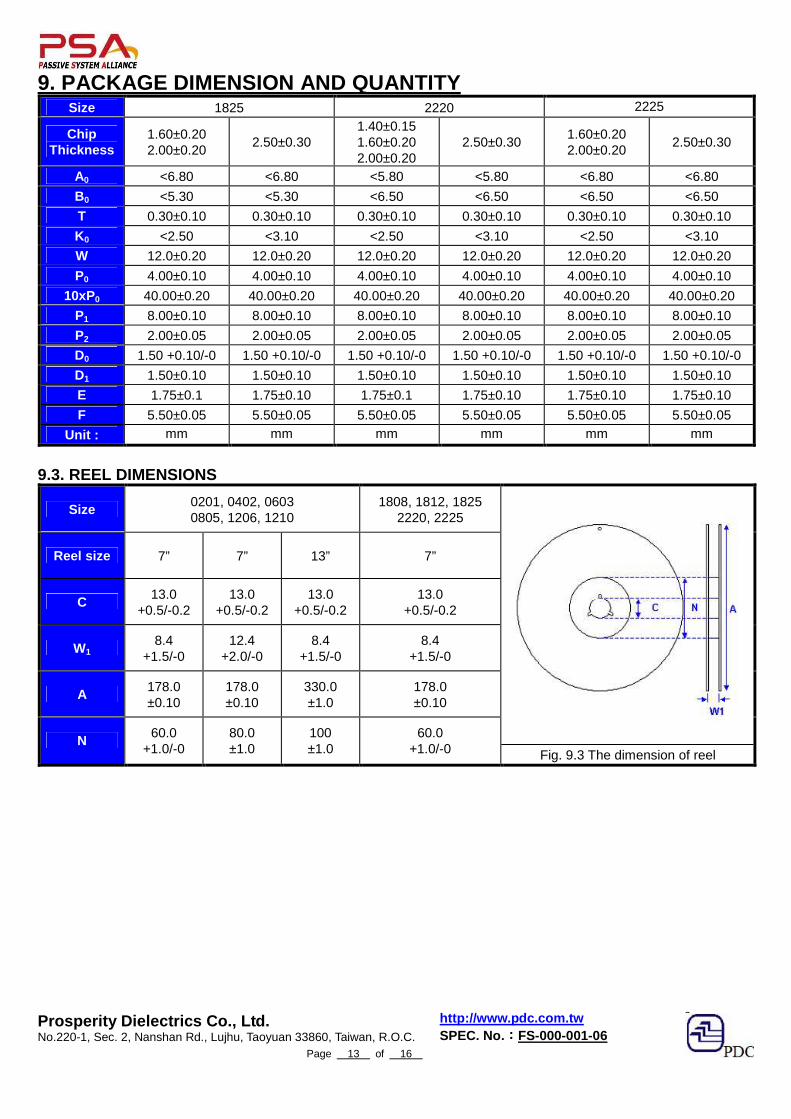
9. PACKAGE DIMENSION AND QUANTITY
Size 1825 2220 2225
Chip Thickness
1.60±0.20 2.00±0.20
2.50±0.30 1.40±0.15 1.60±0.20 2.00±0.20
2.50±0.30 1.60±0.20 2.00±0.20
2.50±0.30
A0 <6.80 <6.80 <5.80 <5.80 <6.80 <6.80
B0 <5.30 <5.30 <6.50 <6.50 <6.50 <6.50
T 0.30±0.10 0.30±0.10 0.30±0.10 0.30±0.10 0.30±0.10 0 .30±0.10
K0 <2.50 <3.10 <2.50 <3.10 <2.50 <3.10
W 12.0±0.20 12.0±0.20 12.0±0.20 12.0±0.20 12.0±0.20 1 2.0±0.20
P0 4.00±0.10 4.00±0.10 4.00±0.10 4.00±0.10 4.00±0.10 4 .00±0.10
10xP0 40.00±0.20 40.00±0.20 40.00±0.20 40.00±0.20 40.00±0 .20 40.00±0.20
P1 8.00±0.10 8.00±0.10 8.00±0.10 8.00±0.10 8.00±0.10 8 .00±0.10
P2 2.00±0.05 2.00±0.05 2.00±0.05 2.00±0.05 2.00±0.05 2 .00±0.05
D0 1.50 +0.10/-0 1.50 +0.10/-0 1.50 +0.10/-0 1.50 +0.10/-0 1.50 +0.10/-0 1.50 +0.10/-0
D1 1.50±0.10 1.50±0.10 1.50±0.10 1.50±0.10 1.50±0.10 1 .50±0.10
E 1.75±0.1 1.75±0.10 1.75±0.1 1.75±0.10 1.75±0.10 1.7 5±0.10
F 5.50±0.05 5.50±0.05 5.50±0.05 5.50±0.05 5.50±0.05 5 .50±0.05
Unit : mm mm mm mm mm mm 9.3. REEL DIMENSIONS
Size 0201, 0402, 0603 0805, 1206, 1210
1808, 1812, 1825 2220, 2225
Reel size 7” 7” 13” 7”
C 13.0 +0.5/-0.2
13.0 +0.5/-0.2
13.0 +0.5/-0.2
13.0 +0.5/-0.2
W1 8.4
+1.5/-0 12.4
+2.0/-0 8.4
+1.5/-0 8.4
+1.5/-0
A 178.0 ±0.10
178.0 ±0.10
330.0 ±1.0
178.0 ±0.10
N 60.0 +1.0/-0
80.0 ±1.0
100 ±1.0
60.0 +1.0/-0 Fig. 9.3 The dimension of reel
http://www.pdc.com.tw Prosperity Dielectrics Co., Ltd. No.220-1, Sec. 2, Nanshan Rd., Lujhu, Taoyuan 33860, Taiwan, R.O.C. SPEC. No.::::FS-000-001-06
Page 13 of 16
2
10. APPLICATION NOTES STORAGE To prevent the damage of solderability of terminations, the following storage conditions are recommended :
Indoors under 5 ~ 40°C and 20% ~ 70% RH. No harmful gases containing sulfuric acid, ammonia, hydrogen sulfide or chlorine. Packaging should not be opened until the capacitors are required for use. If opened, the pack should be re-sealed as soon as is practicable. Taped product should be stored out of direct sunlight, which might promote deterioration in tape or adhesion performance. The product is recommended to be used within 12 months after shipment and checked the solderability before use.
HANDLING Chip capacitors are dense, hard, brittle, and abrasive materials. They are liable to suffer mechanical damage, in the form of cracks or chips. Chip Capacitors should be handled with care to avoid contamination or damage. To use vacuum or plastic tweezers to pick up or plastic tweezers is recommended for manual placement. Tape and reeled packages are suitable for automatic pick and placement machine.
PREHEAT In order to minimize the risk of thermal shock during soldering, a carefully controlled preheat is required. The rate of preheat should not exceed 3°C per secon d.
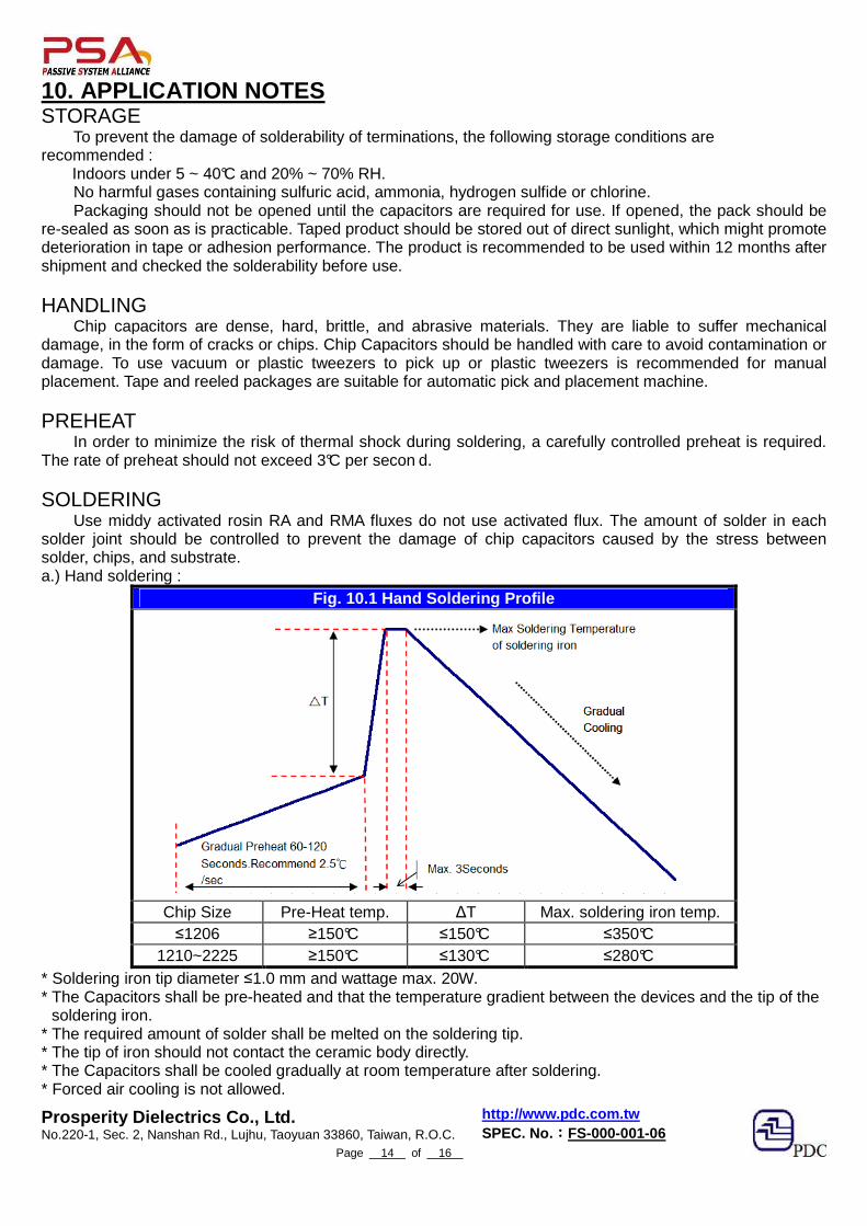
SOLDERING Use middy activated rosin RA and RMA fluxes do not use activated flux. The amount of solder in each solder joint should be controlled to prevent the damage of chip capacitors caused by the stress between solder, chips, and substrate. a.) Hand soldering :
Fig. 10.1 Hand Soldering Profile
Chip Size Pre-Heat temp. ∆T Max. soldering iron temp. ≤1206 ≥150°C ≤150°C ≤350°C
1210~2225 ≥150°C ≤130°C ≤280°C * Soldering iron tip diameter ≤1.0 mm and wattage max. 20W. * The Capacitors shall be pre-heated and that the temperature gradient between the devices and the tip of the
soldering iron. * The required amount of solder shall be melted on the soldering tip. * The tip of iron should not contact the ceramic body directly. * The Capacitors shall be cooled gradually at room temperature after soldering. * Forced air cooling is not allowed.
http://www.pdc.com.tw Prosperity Dielectrics Co., Ltd. No.220-1, Sec. 2, Nanshan Rd., Lujhu, Taoyuan 33860, Taiwan, R.O.C. SPEC. No.::::FS-000-001-06
Page 14 of 16
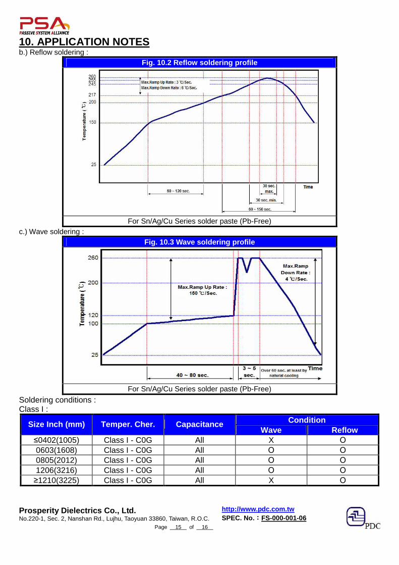
10. APPLICATION NOTES b.) Reflow soldering :
Fig. 10.2 Reflow soldering profile
For Sn/Ag/Cu Series solder paste (Pb-Free) c.) Wave soldering :
Fig. 10.3 Wave soldering profile
For Sn/Ag/Cu Series solder paste (Pb-Free)
Soldering conditions : Class I :
Condition Size Inch (mm) Temper. Cher. Capacitance Wave Reflow
≤0402(1005) Class I - C0G All X О 0603(1608) Class I - C0G All О О 0805(2012) Class I - C0G All О О 1206(3216) Class I - C0G All О О ≥1210(3225) Class I - C0G All X О
http://www.pdc.com.tw Prosperity Dielectrics Co., Ltd. No.220-1, Sec. 2, Nanshan Rd., Lujhu, Taoyuan 33860, Taiwan, R.O.C. SPEC. No.::::FS-000-001-06
Page 15 of 16
10. APPLICATION NOTES Soldering conditions : Class II :
Condition Size Inch (mm) Temper. Cher. Capacitance Wave Reflow
≤0402(1005) Class II - X7R All X О Cap. <2.2µF О О
0603 (1608) Class II - X7R Cap. ≥2.2µF X О Cap. <4.7µF О О
0805 (2012) Class II - X7R Cap. ≥4.7µF X О Cap. <4.7µF О О
1206 (3216) Class II - X7R Cap. ≥4.7µF X О
≥1210 (3225) Class II - X7R All X О Soldering height :
The solder climbing minimum height is suggesting to 25% of chip thickness or 500um whichever is less. (Reference from IPC-610E)
COOLING After soldering, cool the chips and the substrate gradually to room temperature. Natural cooling in air is recommended to minimize stress in the solder joint.
CLEANING All flux residues must be removed by using suitable electronic-grade vapor-cleaning solvents to eliminate contamination that could cause electrolytic surface corrosion. Good results can be obtained by using ultrasonic cleaning of the solvent. The choice of the proper system is depends upon many factors such as component mix, flux, and solder paste and assembly method. The ability of the cleaning system to remove flux residues and contamination from under the chips is very important.
http://www.pdc.com.tw Prosperity Dielectrics Co., Ltd. No.220-1, Sec. 2, Nanshan Rd., Lujhu, Taoyuan 33860, Taiwan, R.O.C. SPEC. No.::::FS-000-001-06
Page 16 of 16