fundamentals of high power impulse magnetron sputtering · fundamentals of high power impulse...
TRANSCRIPT

Linköping Studies in Science and Technology Dissertation No. 1014
Fundamentals of High Power Impulse Magnetron Sputtering
Johan Böhlmark
Plasma & Coatings Physics Division Department of Physics, Chemistry, and Biology
Linköping University, SE-581 83 Linköping Sweden

Cover:
The cover is based on a picture taken through a view port of a vacuum chamber. The blue light
is an Ar/Ti plasma created by a High Power Impulse Magnetron Sputtering (HIPIMS)
discharge.
ISBN: 91-85523-96-8
ISSN: 0345-7524

Abstract
In plasma assisted thin film growth, control over the energy and direction of the incoming
species is desired. If the growth species are ionized this can be achieved by the use of a
substrate bias or a magnetic field. Ions may be accelerated by an applied potential, whereas
neutral particles may not. Thin films grown by ionized physical vapor deposition (I-PVD) have
lately shown promising results regarding film structure and adhesion. High power impulse
magnetron sputtering (HIPIMS) is a relatively newly developed technique, which relies on the
creation of a dense plasma in front of the sputtering target to produce a large fraction of ions of
the sputtered material. In HIPIMS, high power pulses with a length of ~100 µs are applied to a
conventional planar magnetron. The highly energetic nature of the discharge, which involves
power densities of several kW/cm2, creates a dense plasma in front of the target, which allows
for a large fraction of the sputtered material to be ionized.
The work presented in this thesis involves plasma analysis using electrostatic probes, optical
emission spectroscopy (OES), magnetic probes, energy resolved mass spectrometry, and other
fundamental observation techniques. These techniques used together are powerful plasma
analysis tools, and used together give a good overview of the plasma properties is achieved.
Electrostatic probe measurements reveal a dense doughnut shaped plasma expanding from the
erosion zone of the magnetron. The peak plasma density during the active cycle of the discharge
exceeds 1019 electrons/m3. The expanding plasma is reflected by the chamber wall back into the
center part of the chamber, resulting in a second density peak several hundreds of µs after the
pulse is turned off.
Optical emission spectroscopy (OES) measurements of the plasma indicate that the degree of
ionization of sputtered Ti is very high, over 90 % in the peak of the pulse. Even at relatively low
applied target power (~200 W/cm2 peak power) the recorded spectrum is totally dominated by
radiation from ions. The recorded HIPIMS spectra were compared to a spectrum taken from a
DC magnetron discharge, showing a completely different appearance.
Magnetic field measurements performed with a coil type probe show significant deformation in
the magnetic field of the magnetrons during the pulse. Spatially resolved measurements show
evidence of a dense azimuthally E×B drifting current. Circulating currents mainly flow within 2

away cm from the target surface in an early part of the pulse, to later diffuse axially into the
chamber and decrease in intensity. We record peak current densities of the E×B drift to be of the
order of 105 A/m2.
A mass spectrometry (MS) study of the plasma reveals that the HIPIMS discharge contains a
larger fraction of highly energetic ions as compared to the continuous DC discharge. Especially
ions of the target material are more energetic. Time resolved studies show broad distributions of
ion energies in the early stage of the discharge, which quickly narrows down after pulse switch-
off. Ti ions with energies up to 100 eV are detected. The time average plasma contains mainly
low energy Ar ions, but during the active phase of the discharge, the plasma is highly metallic.
Shortly after pulse switch-on, the peak value of the Ti1+/Ar1+ ratio is over 2. The HIPIMS
discharge also contains a significant amount of doubly charged ions.

Preface
The presented research work was conducted since September 2002 in the Plasma & Coatings
Physics Division at IFM, Linköping University, Sweden. It focuses on explaining the
fundamental aspects of the high power impulse magnetron discharge. This work has been
conducted in parallel with work done by Dr Jones Alami and Dr Martina Lattemann under
supervision of Professor Ulf Helmersson. All the experiments have been carried out at IFM,
Linköping University, but I also had the pleasure to collaborate worldwide with numerous
groups in plasma science and thin film growth. To name a few; the Alfven Institute at KTH
Stockholm, Sheffield Hallam University in the UK, the University of Iceland, and the Large
Plasma Laboratory at UCLA in California, US. The Alfven Institute, and the Large Plasma
Laboratory has helped me with constructing and understanding some of my plasma
measurements. The University of Iceland has been involved mostly in data evaluation. The
collaboration with the Sheffield Hallam University has been almost continuous since the start,
and involves most of my work. Thanks to my partners outstanding knowledge in the field of
their research lots of new ideas and explanations arose, and I am very happy for these fruitful
collaborations.
The aim of this work has been to better understand the HIPIMS discharge. A deep
understanding of the features is necessary for a future development and possible
industrialization of the process. This thesis provides a fraction of this understanding, and may
found the basis for some future research in the field. During my time as a PhD student I have
learnt and discovered many things, but it seems the more you learn, the more you realize how
much we do not know.
The investigations presented in this thesis would also not have been possible without the
financial support from the Swedish Foundation for Strategic Research, Swedish Science
Council, and the European Commission.
Linköping March 2005
Johan Böhlmark

Papers included in the thesis I. “Ionization of sputtered metals in high power pulsed magnetron sputtering”
J. Bohlmark, J. Alami, C. Christou, A. P. Ehiasarian, and U. Helmersson
J. Vac. Sci. Technol A 23(1) 18 (2005)
II. “Measurement of the magnetic field change in a pulsed high current magnetron discharge”
J. Bohlmark, U. Helmersson, M. VanZeeland, I. Axnäs, J. Alami, and N. Brenning
Plasma Sources Sci. Technol. 13 654 (2004)
III. “Spatial electron density distribution in a high-power pulsed magnetron discharge”
J. Bohlmark, J. T. Gudmundsson, J. Alami, M. Lattemann, and U. Helmersson
IEEE transactions on plasma science 33(2) 346 (2005)
IV. “The ion energy distributions and ion flux composition from a high power impulse
magnetron sputtering discharge”
J. Bohlmark, J. T. Gudmundsson, Y. A. Gonzalvo, N. Brenning, A. P. Ehiasarian, M.
Lattemann, and U. Helmersson.
Submitted to Thin Solid Films
V. “Investigation of high power impulse magnetron sputtering pretreated interfaces for adhesion
enhancement of hard coatings on steel”
M. Lattemann, A. P. Ehiasarian, J. Bohlmark, P. Å. O. Persson, and U. Helmersson
Accepted for publication in Surface and Coatings Technol. (2005)
VI “Guiding the deposition flux in an ionized magnetron discharge”
J. Bohlmark, M. Östbye, M. Lattemann, H. Ljungcrantz, T. Rosell, and U. Helmersson
Manuscript in final preparation

Contribution to the included papers
Papers I-IV contains predominately my own work, including data collection, evaluation, and
writing. Paper I is based on previous work done by Dr. C. Christou on a different type of
plasma. Dr. Christou also helped in evaluating the experiments, and is therefore included as co-
author. Paper II was originally suggested by Dr M. VanZeeland, who also helped me designing
the probes. A major part of the evaluation and background theory comes from Dr. N. Brenning
and Dr. I. Axnäs at the Alfven Institute at KTH, Stockholm. Paper III is work on the plasma
dynamics done in parallel with similar work done by Dr J. Alami. The massive amount of data
that was collected during the early stages of this paper would not have been possible to acquire
and evaluate without the data collection system and evaluation software. The complete plasma
measurement setup was constructed by our technician Dr. L. Samuelsson in collaboration with
Dr J. Alami and Dr J. T. Gudmundsson. Paper IV contains data collected with an energy
resolved mass spectrometer. I made the measurements and evaluated the data. Dr. Y. Gonzalvo
at Hiden Analytical UK performed some calculations regarding the instrument, and also helped
with the adjustments of the instrument. Paper V is the outcome of a European HIPIMS project.
My contribution to this paper is film growth, etching and an active part of the data evaluation.
Paper VI is the result of a diploma work performed by M. Östbye in collaboration with Impact
Coatings AB. I acted as supervisor for Östbye. Co-authors whose contribution are not
specifically pointed out, have contributed with useful discussions and/or corrections. Naturally,
significant contributions to all my papers have come from my supervisor Prof. U. Helmersson
via discussions, supervision and corrections.

Other related publications (not included) “The ion energy distributions in a high power impulse magnetron plasma”
J. Bohlmark, A. P. Ehiasarian, M. Lattemann, J. Alami, and U. Helmersson
Society of Vacuum Coaters 48th Annual Technical Conference Proceedings (2005)
“Ionization of sputtered Ti during high power pulsed magnetron sputtering”
J. Bohlmark, J. Alami, J.T. Gudmundsson and U. Helmersson
Seventh International Symposium on Sputtering and Plasma Processes ISSP (2003)
"Optical emission study of the ionization fractions in a high power pulsed magnetron plasma"
J. Böhlmark, A. P. Ehiasarian, P. E. Hovsepian, and U. Helmersson
Society of Vacuum Coaters 47th Annual Technical Conference Proceedings, 28-32 (2004)
“Ion-assisted physical vapor deposition for enhanced film properties on nonflat surfaces”
J. Alami, P. O. Å. Persson, D. Music, J. T. Gudmundsson, J. Bohlmark, and U. Helmersson
J. Vac. Sci. Technol. A, 23(2) (2005)
“Plasma parameters during high power pulsed magnetron sputtering”
J. Alami, J.T. Gudmundsson, J. Böhlmark, K.B. Gylfason, and U. Helmersson
Proceedings of the 16th international symposium on plasma chemistry 70, (2003)
“Influence of pressure and power on the composition and time evolution of plasmas in high
power impulse magnetron sputtering”
A. P. Ehiasarian, R. New, P. E. Hovsepian, J. Böhlmark, J. Alami, and U. Helmersson,
Society of Vacuum Coaters 47th Annual Technical Conference Proceedings, 28-32 (2004)
“High power impulse magnetron sputtering (HIPIMS) pre-treatment for the deposition of hard
coatings”
A. P. Ehiasarian. P. Eh. Hovsepian, M. Lattemann, J. Böhlmark, and U. Helmersson
Society of Vacuum Coaters 48th Annual Technical Conference Proceedings (2005)
“Plasma dynamics in a highly ionized pulsed magnetron discharge”
J. Alami, J. T. Gudmundsson, J. Bohlmark, J. Birch, and U. Helmersson

Plasma Sources Sci. Technol. 14 1 (2005)
“Structural analysis and growth of beta and bcc-Ta on inclined surfaces by highly ionized
magnetron sputtering”
J. Alami, P. Eklund, J. M. Andersson, M. Lattemann, E. Wallin, J. Bohlmark, P. Persson, and U.
Helmersson
Submitted for publication
“Ionized Physical Vapor Deposition (IPVD): A review of technology and applications”
U. Helmersson, M. Lattemann, J. Bohlmark, A. P. Ehiasarian, and J. T. Gudmundsson,
Accepted for publication in Thin Solid Films.


Acknowledgements
I would like to express my deepest gratitude to some people who has helped me, encouraged
me, or in some other way contributed to this work. These are:
Ulf Helmersson, my advisor and examiner, for valuable discussions and support and for being a
very nice person. You always gave me a lot of freedom to perform and design my own
experiment. I have really enjoyed working with you!
Martina Lattemann, for a nice collaboration and always taking the time to read and correct my
work. I think you do a great job!
All my friends at IFM. Timo Seppänen, Anders Elfving, and Axel Flink for nice discussions,
golf, and other fun things. We have some great memories to share! Naureen Ghafoor, for
making the lunch break more enjoyable. Per Eklund for help in various problem solving during
courses. Lars Hultman and Jens Birch and all the other members of the thin film group and the
plasma and coatings physics group.
Kalle Brolin, for patiently helping me to build my strange devices. Tomas Lingefelt, for helping
me with the SEM and other equipments. Leif Samuelsson, for help in electrical engineering.
Jon Tomas Gudmundsson, for nice discussions and lots of appreciated help in writing papers.
Nils Brenning and Ingvar Axnäs at the Alfvèn institute, KTH, Stockholm. Our collaboration has
been very fruitful for me. I am very impressed by your structured way of working and your
humble way of expressing your expertise.
Harry (Dr. Arutiun P. Ehiasarian) from the Sheffield Hallam University, for nice discussions
and the collaboration in the HIPIMS project. I hope we can keep a good relation in the future.
Johan Carlsson, Mats Johansson, and Grzegorz Greczynski at Chemfilt Ionsputtering AB,
Sweden, for a good collaboration and the use of their power supply.
To all my co-workers in the field of HIPIMS for nice discussions, to name a few: Bill Sproul,
Dave Christie, Andre Anders, and Yolanda Gonzalvo

Mikael Östbye and Henrik Stranning for nice work performed in their diploma works. Daniel
Lundin and Jan Gluckert, for a well-done project.
All my friends outside university who made my life more enjoyable. I will not mention anyone
specifically because I will only forget someone.
My friends and colleagues in the US: Mike, Christel, Marvin, Simone, Hooman, Klas, Ufuk,
Walter, Steve, David. I have so many great memories with you guys!
Last but certainly not least, my parents, Jan-Erik, and Kristina and my sister Helena, for all the
support I have gotten on the long journey towards my PhD.
If I forgot someone who feels that he or she should be specifically pointed out, please contact
me and I will buy you a dinner…

Contents
1. Introduction 1
1.1 What are thin films? 1
1.2 How to produce thin films? 2
1.3 Aims of this work 3
1.4 Outline of the thesis 4
2. Plasma in thin film growth 5
2.1 What is a plasma? 5
2.2 Plasma used for thin film production 6
3. Basic plasma physics 11
3.1 Plasma ignition 11
3.2 Energy and temperature 11
3.3 Ionization processes 13
3.4 Debye Shielding 15
3.5 Single particle motion 16
4. Plasma analysis 19
4.1 Why plasma analysis? 19
4.2 Main principle of electrostatic probes 19
4.3 Magneto-dynamic probes 22
4.4 Optical emission spectroscopy (OES) 23
4.5 Mass spectrometry 25
5. The magnetron 29
5.1 Background 29
5.2 Basic principle of a planar magnetron 29
5.3 Magnetron operation 32
6. Ionized PVD 35
6.1 Background 35
6.2 Advantages of IPVD 36
6.3 Existing IPVD methods 38
7. HIPIMS 41
7.1 Main principle 41
7.2 Electrical parameters and power supply 42

7.3 Plasma properties 44
7.4 Advantages of HIPIMS 46
7.5 Drawbacks and problems 50
8. Future Outlook 53
8.1 What remains to be understood? 53
8.2 Application areas 54
8.3 Power supplies 55
9. Contribution to the field 57
References 61
Included papers

1. Introduction _______________________________________________________________
1. Introduction
This chapter gives a short introduction to the field of thin
films and how thin films are produced. The aims of this
research are presented and an outline of this thesis is
given.
1.1 What are thin films?
Thin films allow combining the bulk properties of materials with the surface properties of other.
As the demand for high technology products increases, more advanced materials are needed. An
efficient, and most often less expensive way to meet the increased demands is the use of thin
films. Thin films are material layers with thickness ranging from a few atomic layers (~ nm) to
a few micrometers. Thin films as science is quite new, but as art one of the oldest technologies.
Decorative gold leafs from ancient Luxor dating from the Eighteenth Dynasty (about 1500
B.C.) measured 0.3 micrometer in thickness [1]. As a frame of reference for the reader, a human
hair is about 75 micrometer in diameter. Today, thin films can be produced by virtually any
material for a wide range of applications, e.g. optical, decorative, electrical, thermal, wear
protective, and corrosion protective coatings. Thin films in some form are today used in
practically any high-tech product, e.g. semiconductor based electronics, watches, glasses, CD’s,
TV’s, medical equipment, etc. The growth of thin films can be controlled on an atomic scale,
which provides tools for producing materials with outstanding properties. During thin film
growth, individual atoms or ions are deposited onto a surface. By changing the deposition
environment, e.g. temperature or the kinetic energy of the incoming species, the structure and,
thus, the performance of the film can be strongly affected. For instance, thin films can be
produced in crystallographic structures that have outstanding properties, but are not easily
produced in bulk form. As an example, the formation of diamond structure from a bulk graphite
sample requires a huge pressure, whereas the production of a thin diamond like film is a quite
straightforward process.
There are various types of thin films on the market depending on the application. Tribological
(wear protective) films are often produced from metal nitrides, oxides or carbides, such as
AlxOy, TiN or TiC, but a variety of combinations are available [2]. Combining different
1

1. Introduction _______________________________________________________________
elements opens for an opportunity to tailor fit the film for the specific application. For
tribological films, the benefits of a bulk sample and film material are combined. The bulk
sample provides mechanical stability, and the film gives a wear protective inert surface with
reduced friction. Optical and decorative films are used to reflect, transmit, or absorb light [3].
Examples of optical applications are, mirrors of various types, anti-reflection films on glasses or
TV’s, heat flow controlling films on windows, or interference-based films for coloring. A
common decorative film is naturally Au that is expensive in bulk production, but cheap as a thin
film. The most common decorative films are metal oxides and nitrides in various combinations.
Today, films in some form are used in all modern electrical equipment, either to act as
conductor, insulator, or semiconductor.
1.2 How to produce thin films?
There are various ways to produce thin films; electroplating, chemical vapor deposition, heat
evaporation, laser evaporation, plasma assisted evaporation, and a number of combinations of
these methods. See for example reference 4. Electroplating is the deposition of a metallic
coating onto an object by putting a negative charge onto the object and immersing it into a
solution, which contains a salt of the metal to be deposited [5]. The metallic ions of the salt
carry a positive charge and are attracted to the part. When they reach it, the negatively charged
part provides the electrons to "reduce" the positively charged ions to metallic form.
Chemical vapor deposition (CVD) is a process where volatile gases are introduced to react and
form a compound of materials to be deposited. Chemical vapor deposition has been, and still is
within many areas, the most commercially practiced method because it did not require high
vacuum or unusual levels of electrical power [4]. On the other hand, it sometimes relies on or
creates hazardous gases and requires high temperatures, which for some applications is a major
drawback. CVD is only possible when the reactants exist in gas form, which is not always the
case.
Material may also be evaporated from a surface by heating an object. Every material has a
temperature dependent vapor pressure. The vapor pressure is strongly increased if the object is
heated, and the evaporated material can be used for depositions. Adding energy via electrical
energy or a pulsed laser beam can heat the object.
2

1. Introduction _______________________________________________________________
Plasma assisted methods relies on the creation of a plasma in the vicinity of the deposition
source. There are several common plasma assisted deposition techniques and combinations of
them. The two most common are called arc evaporation and magnetron sputtering. Arc
evaporation processes are high-current low DC voltage gas discharges. A very luminous small
cathode spot forms that passes extremely high current densities. This causes erosion of the
cathode by melting and vaporization as well as ejection of solid and molten particles.
Magnetron sputtering is a technique where an external magnetic field is applied to an object to
confine a plasma. Ions from the plasma are used to bombard the surface and evaporate material.
Usually the plasma is sustained by applying a negative voltage to the object and current is
drawn through the plasma. There are a number of ways to apply the voltage to the cathode
depending on the nature of the discharge: DC, Pulsed DC, radio frequency (usually 13.56
MHz), bipolar pulses of various frequencies, and high power pulses. Applying high power
pulses to a magnetron is a relatively new method to produce thin films, and is called High
Power Impulse Magnetron Sputtering (HIPIMS). The technique is also known as High Power
Pulsed Magnetron Sputtering (HPPMS). The terms plasma, magnetron sputtering, and HIPIMS
are described in more detail in the following chapters.
1.3 Aims of this work
The general aim of this work is to explain the nature of the relatively newly developed method
for producing thin films: High Power Impulse Magnetron Sputtering (HIPIMS). Many features
of the method are not, or only partially, understood, and a deeper understanding is necessary for
further development. Today, the technique is mostly used in academia and more fundamental
knowledge about the nature of the process is desired for a full-scale industrial application. A
few important parts of this required knowledge is provided in this thesis. The main objective of
this thesis is to increase the knowledge of process parameters and plasma properties and its
effect on thin film growth. This may lead to a better understanding of the process and an
improvement in film quality. More knowledge of the process helps in the design of new
deposition systems.
Work presented in this thesis is concentrated on the process and the plasma properties. In
HIPIMS, many questions about the process remains to be answered, such as:
• What are the ionization fractions of the sputtered material?
3

1. Introduction _______________________________________________________________
• What is the composition of the plasma? The high power applied to the cathode temporarily
introduces much metal into the plasma. How much?
• What is the plasma dynamics?
• What is the energy of different species in the plasma?
Questions that will be discussed in this thesis are the ionization fractions of sputtered material
and how the high-energy nature of the discharge affects the plasma dynamics and magnetic
properties of the plasma. The ionization fraction of sputtered material is of great importance
when understanding the correlation between plasma properties and film structure. The magnetic
properties of the discharge strongly affect the current path and the impedance of the plasma,
which in turn determines the design of new deposition system and choice of power supplies.
The ion energy distributions from the HIPIMS discharge are presented. The ion energy is
important knowledge in thin film growth since it is strongly connected to the microstructure of
the films. Data collected with various plasma analysis techniques are presented; Langmuir
probe measurements, optical emission spectroscopy, magnetic probes, mass spectrometry, and
other fundamental observations. These techniques used together are powerful plasma analysis
tools, and used together give a good overview of the plasma properties can be achieved.
1.4 Outline of the thesis
The thesis is structured as follows. In chapter 2 the term plasma is introduced and how it can be
used to produce thin films. Chapter 3 contains basic plasma physics, necessary to understand the
included papers. In chapter 4 the basics of the used analysis techniques are presented. In chapter
5 the term magnetron is introduced and explained. Chapter 6 addresses the term Ionized
Physical Vapor Deposition. Chapter 7 introduces the term High Power Impulse Magnetron
Sputtering. Chapter 8 contains my personal view of the future of High Power Impulse
Magnetron Sputtering. In Chapter 9 the contribution to the field is presented. At the end of the
thesis 6 papers are attached.
4

2. Plasma in thin film growth _______________________________________________________________
2. Plasma in thin film growth
This chapter introduces the concept of plasma, and how it
can be used to produce thin films.
2.1 What is a plasma?
Irving Langmuir first introduced the term plasma in 1929 [6] to describe the behavior of ionized
gases in high current vacuum tubes. Plasma is often referred to as the "Fourth State of Matter",
the other three being solid, liquid and gas. Plasma is a distinct state of matter containing a
significant number of electrically charged particles, a number sufficient to affect its electrical
properties and behavior. In an ordinary gas each atom contains an equal number of positive and
negative charges where the positive charges in the nucleus are surrounded by the of negatively
charged electrons, so that each atom is electrically "neutral". A gas becomes plasma when the
addition of heat or other energy causes a significant number of atoms to release some of their
electrons. The remaining parts of those atoms are left with a positive charge, and the detached
negative electrons are free to move about. When enough atoms are ionized to significantly
affect the electrical characteristics of the gas, it is a plasma. The transformation between gas and
plasma is depending on the material and gas pressure, but a typical characteristic of a plasma is
the ability to screen out an internal electric field. Commonly used examples of well-known
plasmas are the aurora borealis (or the northern light), neon signs, fluorescing lights and the
solar corona.
Plasma science underlies numerous important technological applications and devices as well as
our understanding of much of the universe around us. They provide the foundation for present
applications such as plasma processing of semiconductors and thin films, sterilization of
medical products, lamps, lasers, high power microwave sources, and pulsed power switches [7].
They also provide the foundation for important potential applications such as the generation of
electrical energy from fusion as well as for pollution control and removal of hazardous
chemicals [8]. Plasma is believed to make up more than 99 % of the visible universe, including
the sun, the stars, galaxies, and the vast majority of the solar system. Plasma science includes a
variety of science disciplines ranging from plasma physics to aspects of chemistry, atomic and
molecular physics, and material science. Its broad nature also characterizes its plasma physics
component, which includes ionized gases that range from weakly ionized to highly ionized,
5

2. Plasma in thin film growth _______________________________________________________________
from collisional to collisionless, and from cold to hot. These terms characterize various plasmas
ranging from relatively high-pressure gases with a small fraction of the atoms ionized and
relatively low charged-particle temperatures, e.g., plasmas used in computer-chip processing
and light sources, to very low-density gases with a large fraction of the gas atoms ionized and
very high-temperature as such found in fusion plasmas. Fusion plasmas are often considered to
be the energy source of the future [9]. Energy will be released by the same reaction that keeps
all stars alive, fusion of light elements into heavier. This source of energy is believed to replace
conventional nuclear energy in the long-term future. These unique behaviors cause plasmas to
be useful in a large and growing number of important applications in our lives.
Figure 2.1. A neon plasma. Figure courtesy of the Basic Plasma Science Facility at UCLA [10].
2.2 Plasma used for thin film production
Today plasmas are used in a number of ways in the field of thin film production and surface
modification. Consider an object inserted into a plasma. If the object is subjected to a negative
electrical potential compared to the plasma body, the positively charged ions in the plasma will
be accelerated towards the object. At the object surface a number of processes and combinations
of them can occur, see figure 2.2.
6

2. Plasma in thin film growth _______________________________________________________________
Figure 2.2. Effects of bombarding ions or neutral atoms onto a surface. (a) Adsorption, (b)
displacement (momentum transfer), (c) removal of surface atom (sputtering or etching),
(d) ion implantation.
In (a) the arriving ion (or neutral) is adsorbed onto the surface, and a chemical or physical
bonding is created. The incoming specie may also transfer some of its momentum to one of the
surface atoms (b), and cause it to move around on the surface (displacement). If the energy of
the incoming ion is sufficiently high it may start to remove some of the surface atoms
(sputtering, shown in (c)), and if the energy is increased even further, the incoming ion can be
implanted (d). In addition, there can also be a number of combinations of these processes.
Adsorption is typically a low energy process, which is dominant around a few tens of eV, or
less. Sputtering is initiated when the energy of the incoming atom or ion is of the order of 100
eV, while implantation occurs at ~ 1 keV [11]. Naturally, there are no distinct borderlines
between the different processes, but in reality they overlap each other. Also, these processes are
strongly dependent on the chemical and physical properties of the involved atoms and ions.
These processes are important in many plasma assisted thin film growth techniques and found
the basis for most plasma-based applications in the field of thin film growth and surface
modification.
7

2. Plasma in thin film growth _______________________________________________________________
The process where plasma is used to remove material from the solid to be deposited onto a
substrate, is often referred to as physical vapor deposition (PVD) [4]. Where the word
“physical” refers to the use of sputtering, evaporation, ablation etc. Compare to chemical vapor
deposition (CVD), which involves chemical reactions of gases. The removal of material by the
use of a plasma can be done in two ways, sputtering or by the use of an electric arc.
Sputtering is the process where individual ions are impinging onto a surface. When an ion
impact establishes a train of collision events in the target, leading to the ejection of matrix
atoms, we speak of sputtering. Sputtering was first reported in 1852 by W. R. Grove [12]. Since
sputtering is the result of momentum transfer it has been aptly likened to “atomic pool” where
the ion breaks up the close-packed rack of atoms, scattering some backward, to leave the
surface. The principle processes in sputtering are illustrated in figure 2.3.
Figure 2.3. The principle of sputtering. Three energy regimes have been identified. (a) Single knock-on (low
energy), (b) linear cascade, (c) spike (high energy). From P. Sigmund [13].
The exact processes occurring at the target surface is depending on the energy of the incoming
ion. Three different regimes have been identified, (a) Single knock-on (low energy), (b) linear
cascade, and (c) spike (high energy) [13]. The sputtered atoms then become part of the plasma,
as neutral atoms or ions (if they are ionized). The sputtered atoms are then available for
deposition. Sputtering is typically a high voltage, low current discharge (hundreds of volts and
tens of mAcm-2).
The other type of plasma-based thin film production technique is the use of a cathodic arc [14-
16]. Arcs are typically low voltage high current discharges (tens of Volts and hundreds of
8

2. Plasma in thin film growth _______________________________________________________________
Amperes). The discharge can occur in high vacuum, but it should be realized that the term
“vacuum arc” is not physically correct, since in perfect vacuum no arc can exist. The initiation
of a vacuum arc requires two electrodes that first touch and then separates a small distance. A
very small cathode spot is then formed, which carries the discharge. The discharge spot is
typically 10-8 to 10-4 m2 in diameter [4], and carries extremely high current densities (108 to 1012
Am-2 [4,17]). This causes erosion of the cathode spot by melting and vaporization as well as
ejection of molten and solid particles. The local high power density creates a highly ionized
plasma of the cathode material, which then sustain the discharge. The principle of an arc
discharge is shown in figure 2.4.
Figure 2.4. The principle of a cathodic arc. From P. C. Johnson [18].
Today, the most common plasma-based thin film growth techniques are sputtering and cathodic
arc evaporation, and various combinations and versions of them. For sputtering, the most
common method is so called magnetron sputtering, which is addressed in more detail in the
following chapters. Sputtering alone typically produces a low-density, weakly ionized plasma,
whereas cathodic arc produces a dense highly ionized plasma, but a major drawback are the
microdroplets, which reduce the quality of the films when not filtered out.
9

2. Plasma in thin film growth _______________________________________________________________
10

3. Basic plasma physics _____________________________________________________________________
3. Basic plasma physics
This chapter introduces some fundamental physics of
sputtering plasmas. The basic physics needed to
understand the operation of a magnetron is introduced.
3.1 Plasma ignition
To ignite a plasma, a discharge gas is introduced. The gas is often inert, to avoid unwanted
reactions with the target material, but can also contain a fraction of a reactive gas if a compound
film is desired. The most common gas used in sputtering processes is Ar, mixed with N2 or O2.
An electric field is then applied between the sputtering source (cathode) and an anode. Often,
the chamber wall is used as anode in the system. Even at room temperature, the gas will contain
a small fraction of ions and some free electrons (from background radiation). The ions and
electrons are then accelerated towards the cathode and the anode respectively. The electrons
then generate new ions and electrons via collisions with the gas atoms. In addition, new
electrons are also generated at the cathode surface. When the ions reach a close distance from
the cathode surface (a few Angstroms), electrons can tunnel from the cathode, and the ions are
neutralized. When an ion is neutralized, the energy corresponding to the ionization energy of the
ion is released. This energy can then be given to a surface electron, via an Auger process. If the
ionization potential of the ion is greater than the electron work function, new electrons can be
emitted into the gas. These electrons are so-called secondary electrons. Electrons are then
accelerated by the electric field, and generate new ions and free electrons. By the addition and
acceleration of new electrons. an “avalanche” of ionizations has started. If the applied power is
sufficiently high, a plasma is created. This process is called plasma breakdown. The plasma
then adjusts itself regarding temperature, density, and distribution in space until it reaches a
balance between charge losses and supplied energy.
3.2 Energy and temperature
A gas at thermal equilibrium has particles of all velocities, and the most probable distribution of
those velocities is the Maxwellian distribution. The one-dimensional Maxwellian distribution is
given by
11

3. Basic plasma physics _____________________________________________________________________
( )kT2/muexpA)u(f 2−= (1)
where f(u) is the number of particles with velocity between u and u+du, mu2/2 is the kinetic
energy, and k is Boltzmann’s constant [19]. The constant A is related to the density n by
5.0
kT2mnA ⎟
⎠⎞
⎜⎝⎛
π= (2)
The average kinetic energy (Eav) of a Maxwellian distribution is kT/2 per degree of freedom.
Since T and Eav are so closely related, it is common in plasma physics to give temperature in
units of energy [20]. To avoid confusion on the number of dimensions involved, it is not Eav,
but the average corresponding to kT that is used to denote the temperature. For example if we
have kT = 1 eV = 1.602 × 10⁻¹⁹ J, we have
K 116001038.110602.1T 23
19
≈××
= −
−
(3)
Thus, the conversion factor is 1 eV ≈ 11600 K. In many processing plasmas several
temperatures can exists at the same time. Often the ions and the electrons have Maxwellian
distributions with different temperatures. In most cases, the energy to the plasma is supplied via
energetic electrons. The moment transfer efficiency is relatively low, due to the large
differences in mass. Then each species can have its own thermal equilibrium, but the lifetime of
the plasma species is not long enough for the two temperatures to equalize. In the presence of a
magnetic field, the temperature can also be different in different directions.
Furthermore, a common misunderstanding is that a high temperature is directly connected to
lots of heat. However, most plasmas are created in a low pressure environment with very little
heat capacity. The electron temperature inside a common neon sign is several tens of thousands
of degrees, but still does not melt the glass. This is because the electrons can transfer very little
energy to the glass, due to the low pressure and their low mass.
12

3. Basic plasma physics _____________________________________________________________________
3.3 Ionization processes
The ionization in a sputtering plasma relies on several different phenomena. The three most
important responsible for the generation of ions in an inert gas plasma are electron impact
ionization of neutral atoms, electron impact ionization of an excited atom, and Penning
ionization by collision with an electronically excited atom according to [21]
−− +→+ 2eIoneAtom −− +→+ 2eIoneAtom*
AtomeIonAtomAtom * ++→+ − (Penning)
For high-density plasmas (ne > 1017 m-3) the electron impact ionization of neutral atoms is the
dominating process [21] and will therefore be the only subject for discussion in this thesis. The
mean ionization distance from electron impact ionization can be determined according to [21].
)(TKnvλ
eie
Miz = (4)
where vM is the velocity of the sputtered atom, ne is the density of electrons, and Ki(Te) is the
ionization rate constant according to
e0
kTE
0ei eK)(TK−
= (5)
where K0 and E0 are material dependent and available in literature for some materials [22-27].
Atoms sputtered from the surface of the cathode typically follow the Thompson distribution
with average energies of the order of a couple of eV, corresponding to velocities of about 103
m/s [28]. We can now estimate the average distance an atom travels before it suffers an ionizing
collision by using equation 4 and 5. An example calculated for Cu and C is illustrated in figures
3.1 and 3.2. From figures 3.1 and 3.2, it is realized that the mean ionization distance for a
sputtered particle is strongly material dependent. In order to reduce the expected ionization
distance for Cu so that it matches the dimensions of the highly energetic plasma (~cm) [29,30],
we require plasma densities of the order of 1019 m-3 and electron temperature of around 3 eV.
For C these values are even higher. The difference is due to the higher ionization potential and
smaller cross section of the carbon atom.
13

3. Basic plasma physics _____________________________________________________________________
12
34
5 10^1710^18
10^19
-2
-1
0
1
2
3
Plasma density (m-3)Electron energy (eV)
log(λ iZ) (m)
Figure 3.1. The calculated mean ionization distance λiZ for a sputtered Cu atom as a function of plasma
density and electron temperature.
12
34
5 10^1710^18
10^19
-1
0
1
2
3
4
5
Plasma density (m-3)Electron energy (eV)
log(λ iZ) (m)
Figure 3.2. The calculated mean ionization distance λiZ for a sputtered C atom as a function of plasma
density and electron temperature.
To achieve an effective ionization of the deposition material in sputtering processes, it is,
therefore, necessary to apply enough electrical power to reach electron densities of the order of
1019 m-3, while the electron temperature should be at least a few eV. In reality this corresponds
to a power of the order of kWcm-2 on the target surface. Usually this amount of power cannot be
applied constantly, due to insufficient cathode cooling, but has to be applied in pulses with a
14

3. Basic plasma physics _____________________________________________________________________
low duty factor. The duty factor is defined as the ratio between pulse on time and the total cycle
time.
3.4 Debye shielding A fundamental characteristic of a plasma is its ability to shield out an externally applied electric
field. If an electric field were applied to a plasma, by inserting two electrodes. The two
electrodes attract charge carriers of the opposite charge, and a “cloud” of electrons and ions will
surround each electrode.
Figure 3.3. The principle of Debye shielding.
For a very cold plasma, with no thermal motion of the charge carriers, the electric field of the
electrodes would be totally shielded. No electric field would be present inside the plasma body.
If the temperature is finite, however, some of the ions and electrons at the edge of the cloud
could escape the attractive force of the electrode. In this case, some of the electric field will
penetrate into the plasma. The region where the electric field penetrates the plasma is called a
sheath. The thickness of a sheath is of the order of the Debye length λD. The Debye length is
defined as
5.0
2e0
D nekT
⎟⎠⎞
⎜⎝⎛ ε=λ (6)
15

3. Basic plasma physics _____________________________________________________________________
where Te is the electron temperature, n is the plasma density [20]. Expression 6 can in a
simplified form be written as λD = 69(Te/n)0.5 m, where Te is given in Kelvin. Sheaths appear
where a plasma meets a solid such as a chamber wall, electrode, substrate, or probe. The
thickness of a sheath depends on the potential difference between the solid surface and the
plasma potential [31]. The Debye length is an important parameter in processing plasmas since
it describes a plasmas ability to penetrate into holes, and the behavior of the plasma around
inserted objects.
3.5 Single particle motion
Consider a charged particle with charge q moving in a magnetic and electric field denoted B and
E respectively. The equation of motion for this particle is then
)(qdtdm BvEv
×+= (7)
We choose E to lie in the x-z plane so that Ey = 0 and B is assumed to be only in the z-direction,
resulting in
zz E
mq
dtdv
= (8)
which is a straight forward acceleration along B. The transverse components of equation 7 are
ycxx vE
mq
dtdv
ω±= (9)
xcy v
dtdv
ω±= 0 (10)
which by the use of differentiation can be solved as
tix
cevv ω⊥= (11)
BE
eivv xtiy
c −±= ⊥ω (12)
v⊥ is the velocity component perpendicular to B and ωc is the so called cyclotron frequency (ωc
= qB/m). Equation 8, 11, and 12 describes an oscillating motion around a drifting center. The
radius of each oscillation is often referred to as the Larmor radius rL and the “position” in which
the particle oscillates around is called the guiding center. The Larmor radius rL is defined as
[20]
16

3. Basic plasma physics _____________________________________________________________________
qBmvrL = (13)
Figure 3.4 shows the expected trajectory of a particle moving in a crossed magnetic and electric
field.
Figure 3.4. Particle drifts in crossed magnetic and electric fields. From F. Chen [20].
The drift of the guiding center of the particle is denoted vgc. The velocity of the guiding center
can be calculated according to [20]
2gc BBEv ×
= (14)
It is important to notice that the direction of vgc is independent of q, m, and v in the case of
uniform B and E fields. Ions and electron drift due to the E field in the same direction, but
oscillating around their guiding centers in different direction. However, it should be noted that
since ions have much greater mass, they exhibit a much greater Larmor radius, in many cases
even bigger than the dimensions of the plasma.
17

3. Basic plasma physics _____________________________________________________________________
18

4. Plasma analysis _______________________________________________________________
4. Plasma analysis
This chapter introduces the fundamentals of plasma
diagnostics. Four different plasma-probing techniques are
addressed; electrostatic probes, magneto dynamic
probes, optical emission spectroscopy, and mass
spectrometry.
4.1 Why plasma analysis?
A plasma can be characterized by a number of properties such as number of ionized species per
volume (density), temperature of ions and electrons, degree of ionization, ion and neutral
composition, and dynamics. Plasma analysis is important in any plasma assisted thin film
deposition technique, since the processes occurring during the material transport through the
plasma directly affects the properties of the arriving flux regarding incident energy and
direction, and ionization. This in turn strongly affects the properties of the films [32,33]. The
experimental methods best suited, depends on which feature that one wants information about.
In this work 4 different major plasma probing techniques were used; electrostatic probes,
magneto dynamic probes, optical emission spectroscopy (OES), and mass spectrometry. These
techniques combined are very powerful, and can give a complete picture of the plasma
parameters. The typical features of each technique are described in more detail in the following
sections.
4.2 Main principle of electrostatic probes
Electrostatic probes are often referred to as Langmuir probes. The name comes from the
American scientist Irving Langmuir working with low-pressure discharges. He was awarded the
Nobel Prize in Chemistry 1932 for his discoveries. The technique relies on the insertion of one
or several electrodes into the plasma. The electrode is then biased with various potentials and
the current drawn from the plasma body is measured. The current drawn from the plasma body
is mainly depending on the applied bias, the density of the plasma, and the temperature of ions
and electrons. In the type of plasma discussed in this thesis, the current drawn by a Langmuir
probe is mainly electron based, since the electrons have much higher mobility than ions. Thus,
Langmuir probe measurements can give information about the plasma density and electron
19

4. Plasma analysis _______________________________________________________________
temperature. Spatially resolved measurements can also give information about the plasma
dynamics as a collective media. A schematic of a single tip Langmuir probe can be seen in
figure 4.1.
Ceramic tubes
Tungsten wire A
Figure 4.1. A single tip Langmuir probe.
A plasma confined in a vacuum chamber constantly looses some of its electrons and ions to the
grounded walls. Assume that the plasma body initially is at ground potential. Since electrons are
smaller and lighter than the ions, more electrons compared to ions will be lost via diffusion to
the chamber walls. This will charge up the plasma body and a potential sheath will develop
between the plasma and the chamber wall. The sheath will repel some of the electrons. As a
result, the plasma body charges up until the loss of electrons and ions is the same. The potential
at which the loss of ions is the same as the loss of electrons, is referred to as the plasma
potential (Vp). Usually the plasma potential is of the order of a few volts (positive) in the type of
plasma discussed in this thesis. In the absence of magnetic fields inside the bulk plasma, the
plasma potential is usually constant throughout the whole plasma. When a magnetic field is
present, the situation might be a bit different. In this case, the plasma potential does not need to
be constant through the whole plasma, and may also locally be negative [29].
Now consider a Langmuir probe inserted into the plasma. If the probe is left electrically
insolated, no charge carries can escape, and the probe is charged up. Again, since electrons are
more mobile, more electrons than ions will reach the probe surface and the probe will charge up
negatively. The potential at equilibrium is reached is called the floating potential (Vf). The
floating and plasma potential are important parameters in coating plasmas, since they indirectly
affect how the films are formed. If the probe is connected to a power source, such as a battery or
a variable power supply, a current will flow trough the probe. If a large negative potential is
applied to the probe compared to the plasma potential, the probe will attract the positively
charged ions. The large potential barrier between the plasma and the probe will repel all
20

4. Plasma analysis _______________________________________________________________
electrons. Ions that reach the probe surface will be neutralized with an electron from the probe.
In this process secondary electrons may also be ejected. This result in that a current will flow
through the plasma and the probe, usually referred to as ion current, although it is only carried
by ions inside the plasma, and at the probe surface. As the potential applied to the probe is
decreased, some highly energetic electrons can overcome the potential barrier between the
plasma and the probe. When the probe potential has dropped to a level where as many electrons
reach the probe from thermal motion, as ions are attracted, the probe is at the floating potential.
If the probe potential is made even more positive, more and more electrons start to reach the
probe, and the total current changes direction, so called electron current. The electron current is
electron based throughout the whole circuit. When the probe potential is further increased, and
reached the plasma potential, all electrons can reach the probe. Increasing the potential even
further, the probe now attracts all electrons, and the current is steadily increasing. Due to the
higher mobility of electrons, the electron current is usually 1-3 orders of magnitudes higher than
the ion current. The shape of the current as function of applied probe voltage is often referred to
as probe I-V curve. A schematic of a probe I-V curve can be seen in figure 4.2.
-15 -10 -5 0 5 10 15
0
1
2
3
4
VpVf
Pro
be c
urre
nt (m
A)
Probe voltage (V) Figure 4.2. An example of a Langmuir probe I-V characteristics.
21

4. Plasma analysis _______________________________________________________________
From the Langmuir probe characteristics, the electron temperature (or in fact the whole energy
distribution function) and the plasma density can be estimated. A number of theoretical
approaches to evaluate I-V traces exist, as the one shown in figure 4.2 [see for example ref. 20,
34,35]. Druyvesteyn first developed the theory used in this thesis during the 1930’s [36]. The
theory developed by Druyvesteyn allows for an estimation of the electron energy distribution
function (EEDF) according to
2
25.0
pr2e dV
IdmeV2
Aem2f ⎟
⎠⎞
⎜⎝⎛= (1)
where m is the electron mass, e is the elementary charge, Apr is the area of the probe, and V is
the difference between the plasma potential and the probe potential. The plasma density can
then be extracted from equation 1, by integrating over all energies up to the plasma potential.
The theory does not take into account that an ion current is also present, but the error generated
by this assumption is expected to be minor.
4.3 Magneto-dynamic probes
Magneto-dynamic probes are used to determine how currents are flowing inside a plasma. The
current flowing in a plasma is due to the relative motion of the ions and electrons. Assuming
that all ions are positively charged (which is common, but not always the case), the current
density, j, can be defined as
ne)( ie uuj −−= (2)
where u is the drift velocity of electrons and ions, respectively, and n is the electron density.
Thus, currents are present in the bulk plasma if the relative motion of ions and electrons is
different. This is often the case, especially in the presence of magnetic fields, since the
properties of electrons and ions are so different. The ions are less mobile and heavier than the
electrons, and therefore much less affected by magnetic fields, or other perturbations. The
currents flowing in a plasma generates magnetic fields, which in turn can be detected.
Typically, a plasma is considered to be of diamagnetic nature, meaning that currents tend to
flow in way that generates magnetic fields that opposes an externally applied field. The relation
between a magnetic vector field and current is
22

4. Plasma analysis _______________________________________________________________
Bj ×∇=µ0 (3)
which allows for calculation of the current density with same spatial resolution as the magnetic
vector field [see for example ref 37]. The most common ways to detect currents in a plasma is
by using a Hall probe or a B-dot probe. The Hall probe relies on the Hall effect [37], and can be
used to measure both DC and AC components of the current. The B-dot probe can only be used
to record the AC component of the field, but is the more commonly used in pulsed plasmas. The
B-dot probe is usually a quite simple device, which is basically a small coil. The magnetic field
change generated by a pulsed plasma can then be detected by the coil according to
dtdB(t)NA)t(U = (4)
where N is the number of turns in the coil, A is the cross section area, and U is the induced
voltage by the magnetic field. In practice, often two coils are used with the same area but
opposite winding direction. Pulsed plasmas often contain high frequency electric field
components, which can penetrate through the probe insulation and disturb the measurement.
This problem can be overcome by using double winding. The electrostatic charging by the
plasma is the same for the two coils, but the magnetically induced voltage has opposite sign. By
taking the difference in the recorded voltage between the two windings, the magnetically
induced component can be extracted. The B-dot probe is an important experimental device to
extract information about the plasma dynamics, the transport of charged particles in pulsed
plasmas and other dynamic phenomena in plasmas.
4.4 Optical emission spectroscopy (OES)
Spectroscopy is the study of spectra, i.e. characteristic wavelengths or colors. In optical
emission spectroscopy (OES), the light emitted by atoms and ions in the wavelength range from
about 100 nm to 900 nm are recorded. This range includes the ultraviolet, and visible light
(from violet at 380 nm to red at 760 nm), and the near infra-red range. Light is electromagnetic
radiation generated by the acceleration of charged particles or by transitions of electrons in
atoms and ions. In a plasma, the free plasma electrons creates excited states, which recombine
23

4. Plasma analysis _______________________________________________________________
and sends out photons. The excited states are usually created by electron excitation, but can also
be created by a photon.
Figure 4.3. The generation of light gives a fingerprint of the species in the plasma.
The photons sent out from a plasma can then give a fingerprint of the species in the plasma,
since every atom and ion has different electron energy levels. OES is a very powerful, but also
very complicated analysis technique, where several plasma properties can be extracted. In the
simplest approach, a qualitative study of the species in the plasma can be performed. The light
is recorded and divided into wavelength components by a spectrometer. Each wavelength
component then corresponds to an atomic energy level according to
λ=
hcE (5)
where h is Plank’s constant, c is the speed of light, and λ is the wavelength. The energy levels
of various atoms and molecules are quite well documented [38-41], so an identification of the
emitting species is quite straightforward. A quantification is, however, more difficult to obtain.
The recorded intensity of an individual emission line is dependent on several things such as
excitation mechanism, atomic transition probability, re-absorption of the emitted photons, and
spectrometer sensitivity for the different lines. In a plasma, the main excitation mechanism is
excitation by one of the energetic free plasma electrons. The relative intensity of various
emission lines is an indirect mapping of the distribution of excited states of different ions and
24

4. Plasma analysis _______________________________________________________________
atoms. The distribution of excited states is then in turn mainly generated by electron collisions.
Thus one can, by studying the emission spectrum of individual specie, get information about the
energy distribution of the plasma electrons [42]. With knowledge of the distribution of excited
states, and the transition probabilities, quantitative estimations are also possible with OES [43-
45]. It is also possible to estimate the temperature of ions and neutrals, using the Doppler shift.
Highly energetic ions and neutrals will create broader emission peaks. This however requires a
high-resolution spectrometer.
In principle, there are two main types of spectrometers; prism based and grating based. In prism
spectrometers, the light is passed through a slit, and divided into wavelength components via a
prism. The principle is shown in figure 4.4.
Figure 4.4. The principle of prism based spectrometers. After K. Krane [46].
The other type of spectrometers is grating based. The light is projected onto a grating, and a
camera records the reflected light. The reflected light from a grating will form a diffraction
pattern, and can via a computer algorithm be transferred to a spectrum.
4.5 Mass spectrometry
Mass spectrometry of a plasma is the extraction and detection of individual plasma species, ions
or neutrals. An extraction probe is inserted into the plasma, into which gas atoms and ions from
the plasma may enter. If neutral atoms are to be analyzed, they first have to be ionized in the
instrument. The ions are then passed through a series of filters and electrostatic lenses, and then
25

4. Plasma analysis _______________________________________________________________
detected. Mass spectrometry can also be energy resolved. The principle of mass spectrometry is
illustrated in figure 4.5.
Figure 4.5. The main principle of plasma mass spectrometry.
The whole system is usually separately pumped in order to increase the mean free path for the
ions inside the device. The extraction part is simply a small hole (~ 50 – 300 µm diameter)
where ions and neutrals can pass through. The front can be electrically floating biased or
grounded. Inside the extraction orifice, an ionization source is situated. This is usually a heated
filament that emits electrons. The next two parts (energy and mass filter) of a spectrometer is
depending on the type of mass spectrometer. There are two main types of spectrometers; Time-
of-Flight (TOF), and spectrometers based on electrostatic filters.
A TOF mass spectrometer uses the differences in transit time through a drift region to separate
ions of different masses. It operates in a pulsed mode so that ions have to be produced or
extracted in pulses. An electric field accelerates all ions into a field-free drift region with a
kinetic energy of qV, where q is the ion charge and V is the applied voltage. Since the ion
kinetic energy is mv2/2, lighter ions have a higher velocity than heavier ions and reach the
detector at the end of the drift region earlier. Since the flight time is also depending on the
kinetic energy of ions entering the device, there is also information available about the ion
energy distribution by studying the peak broadening.
Mass spectrometers based on electrostatic filters divides the energy and the mass filtering into
two parts. The energy filter is generally a quite simple device, where only ions of certain energy
26

4. Plasma analysis _______________________________________________________________
may pass through, for example a so-called Bessel box. A schematic of a Bessel box is shown in
figure 4.6. Ions with too high or low energy (B and C) will not travel through the filter.
Figure 4.6. The main principle of a Bessel box.
The mass filter is a bit more complicated. The most common mass filter is a so-called
quadrupole. A quadrupole mass filter consists of four parallel metal rods arranged as in figure
4.7. Two opposite rods have an applied potential of (V+Asin(ωt)) and the other two rods have a
potential of -(V+Asin(ωt)), where V is a dc voltage and Asin(ωt) is an AC voltage. The applied
voltages affect the trajectory of ions traveling down the flight path centered between the four
rods. For given dc and ac voltages, only ions of a certain mass-to-charge ratio pass through the
quadrupole filter and all other ions are thrown out of their original path. A mass spectrum is
obtained by monitoring the ions passing through the quadrupole filter as the voltages on the
rods are varied. There are two methods: varying ω and holding V and A constant, or varying V
and A (V/A) fixed for a constant ω.
27

4. Plasma analysis _______________________________________________________________
Figure 4.7. The principle of a quadrupole mass filter.
28

5. The magnetron _______________________________________________________________
5. The magnetron
This chapter introduces the functionality of a planar
magnetron. The basis principles are explained.
5.1 Background
In a basic sputtering process, a target plate is bombarded by energetic ions generated in a glow
discharge plasma situated in a close vicinity. The rate of material leaving the target is depending
on the number of bombarding ions. It is therefore desired to increase the plasma density in front
of the sputtering source. Basic sputtering without any plasma confinement has the
disadvantages of low deposition rates and low ionization efficiencies of the plasma. These
limitations have lead to the development of magnetron sputtering. The magnetron was first
introduced in the early 70s [47-49], and has rapidly developed to the point where it has become
the number one choice for the deposition of a wide range of industrial coatings. The driving
force behind the development of magnetron sputtering has been the increasing demand of high-
quality functional thin films in widespread application areas. Magnetron sputtering now makes
a significant impact in a large number of application areas including hard, wear-resistant
coatings, decorative coatings, and coatings with specific optical or electrical characteristics. The
basic sputtering process was known, and used for many years despite its limitations. However,
it was the development of the magnetrons in various forms, which really arouse the importance
of sputtering. Magnetron sputtering today exists in a number of forms regarding geometry and
electrical power, all depending on the application. As in any plasma based deposition process it
is possible to grow high quality films at low temperatures using magnetron sputtering since the
ions from the plasma can be used for films densification and formation of metastable phases.
5.2 Basic principle of a planar magnetron
Magnetrons make use of the fact that a magnetic field configured parallel to the target surface
can constrain the motion of secondary electrons ejected by the bombarding ions, to a close
vicinity of the target surface. An array of permanent magnets is placed behind the sputtering
source. The magnets are placed in such a way that one pole is positioned at the central axis of
the target, and the second pole is placed in a ring around the outer edge of the target. A
schematic of the magnetron is shown in figure 5.1.
29

5. The magnetron _______________________________________________________________
Figure 5.1. The principle of a magnetron. From M. Ohring [4].
This configuration creates crossed E and B fields, where electrons drift perpendicular to both E
and B according to vH = E/B. If the magnets are arranged in such a way that they create closed
drift region, electrons are trapped, and relies on collisions to escape. By trapping the electrons in
this way, the probability for ionization is increased by orders of magnitudes. Ions are also
subjected to the same force, but due to their larger mass, the Larmor radius often exceeds the
dimensions of the plasma. Although in general one says that the ions are not directly confined,
they are so indirectly by trapping the electrons, to keep the quasi neutrality of the plasma. The
trapping of electrons and ions creates a dense plasma, which in turn leads to an increased ion
bombardment of the target, giving higher sputtering rates and, therefore, higher deposition rates
at the substrate. The electron confinement also allows for a magnetron to be operated at much
lower voltages compared to basic sputtering (~ 500 V instead of 2-3 kV) and be used at lower
pressures (typically mTorr region). This is an advantage since less material is lost to the
chamber wall and back to the target through scattering in the discharge gas. The shape of the
magnetic field efficiently erodes the target where the magnetic field lines are parallel to the
target surface, a so-called race-track is created. A picture of a sputtered circular target is shown
in figure 5.2.
30

5. The magnetron _______________________________________________________________
Figure 5.2. A sputtering target.
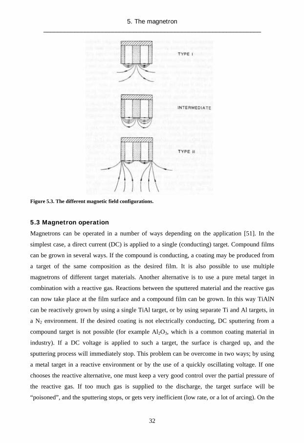
The magnetic field configuration of magnetrons can be divided in three different categories;
intermediate (balanced), and unbalanced type I and II. The differences in design between the
different categories are only slight. However, the difference in performance regarding film
growth between the different types can be significant. During film growth it is often desired to
have an effective ion bombardment of the film. This can be achieved by applying a bias onto the
substrate. In most cases it is preferred to have a high ion current containing low energy ions,
rather than high energy, since this can generate stress and defects in the film [50]. It is therefore
desired to design the magnetic field in such a way that it allows for some of the plasma to
escape from the close vicinity of the cathode, and reach the substrate. This is the reason for the
different magnetron designs. A schematic of the three different designs are illustrated in figure
5.3.
31
5. The magnetron _______________________________________________________________
Figure 5.3. The different magnetic field configurations.
5.3 Magnetron operation
Magnetrons can be operated in a number of ways depending on the application [51]. In the
simplest case, a direct current (DC) is applied to a single (conducting) target. Compound films
can be grown in several ways. If the compound is conducting, a coating may be produced from
a target of the same composition as the desired film. It is also possible to use multiple
magnetrons of different target materials. Another alternative is to use a pure metal target in
combination with a reactive gas. Reactions between the sputtered material and the reactive gas
can now take place at the film surface and a compound film can be grown. In this way TiAlN
can be reactively grown by using a single TiAl target, or by using separate Ti and Al targets, in
a N2 environment. If the desired coating is not electrically conducting, DC sputtering from a
compound target is not possible (for example Al2O3, which is a common coating material in
industry). If a DC voltage is applied to such a target, the surface is charged up, and the
sputtering process will immediately stop. This problem can be overcome in two ways; by using
a metal target in a reactive environment or by the use of a quickly oscillating voltage. If one
chooses the reactive alternative, one must keep a very good control over the partial pressure of
the reactive gas. If too much gas is supplied to the discharge, the target surface will be
“poisoned”, and the sputtering stops, or gets very inefficient (low rate, or a lot of arcing). On the
32

5. The magnetron _______________________________________________________________
other hand, if one does not supply enough gas, the compound will not form with the right
stoichiometry. The partial pressure must, therefore, be controlled so that it keeps the pressure at
a level where the target is kept relatively “clean” by the sputtering, but there is enough gas to
form the desired stoichiometry. This can be a quite complicated and unstable process. The other
alternative is to use an alternating voltage of some kind (pulses or other type of oscillating
voltage). The two most common ones are rf frequency sputtering (usually 13.56 MHz) or
bipolar pulsed sputtering. In rf sputtering most materials can be used as cathode, but the
deposition rate is usually very low. In bipolar pulsed sputtering, the voltage is reversed for a
short time. This attracts some of the electrons from the plasma, and neutralizes the charge that
has accumulated on the target surface. Since the electrons have so high mobility, it is usually
only necessary to have a reversed bias supplied for 10 – 20 % of the time.
33

5. The magnetron _______________________________________________________________
34

6. Ionized PVD _______________________________________________________________
6. Ionized PVD
This chapter introduces the concept of Ionized Physical
Vapor Deposition (IPVD). The basics and features of
various techniques are mentioned.
6.1 Background
State of the art sputtering processes allow for the deposition of materials for a large number of
applications. There is a constantly increasing demand for the development of coatings with
tailored and enhanced properties such as high hardness, wear and corrosion resistance, low
friction, and specific electrical or optical behavior. For high-quality coatings there is a lot of
room for improvements using versatile PVD processes. An important feature of plasma based
PVD processes is the availability of bombardment of plasma ions during film growth [see for
example ref 52 and 53]. Bombarding ions transfer momentum to the surface, which in many
cases is a great advantage during low temperature film growth. An optimized ion bombardment
has beneficial effects on the microstructure, which in turn often leads to improved mechanical
and chemical properties of the coating. The increasing requirements on coatings and the process
techniques drive the development of enhanced deposition techniques, which allows better
control of the flux of material and further decrease in deposition temperature. Common
sputtering processes have ions available for momentum transfer, but mainly ions of the
discharge gas whereas ions of the sputtered material are relatively rare. For many applications it
is desired to have also ions of the sputtering material, since this allows for an effective ion
bombardment and control over energy and direction. It can also be a powerful tool in other
surface modification processes such as etching and implantation.
Over the last years various techniques have been developed that ionizes the material flux. When
the flux of ions is higher than the flux of neutrals of the sputtered material at the substrate, the
process is referred to as IPVD [21]. The development of IPVD techniques was initially mainly
driven by the need to deposit metal layers and diffusion barriers into trenches and vias of high
aspect ratio IC structures [54-56], but has during the last years found a number of areas where
beneficial effects were observed.
35

6. Ionized PVD _______________________________________________________________
6.2 Advantages of IPVD
The main advantage by using IPVD is the versatility. One gets an “extra knob” to turn to vary
the direction and energy of the deposition flux. The energy and direction of incoming ions are
important parameters in thin film growth [see for example ref 33].
In trench filling it is desired to have a collimated flux towards the opening of the hole, and
effective re-sputtering at the corners of the opening of the trench. This is possible if a large
fraction of the deposition flux is ionized. A figure 6.1 show the filling of trench with an ionized
flux of Cu. β is defined is the ionized flux fraction. It is seen that for increasing ionized flux, the
trench is filled better. The control over direction can be utilized in any deposition process where
the substrate is complex shaped.
Figure 6.1. The metallization of a trench with IPVD. From Lu and Kushner [57].
Another key feature of thin films is that in general a dense microstructure is desired. This is
effectively achieved with a highly ionized flux of deposition material and a substrate bias. The
highly ionized flux gives an effective film densification during film growth, with a dense, less
columnar microstructure. The dense structure may reduce the friction of the coating, increase
the mechanical performance, and increase the resistance against corrosion. Figure 6.2 shows
two films (TiC/CaO) grown under the same conditions. In (a), the degree of ionization is low,
36

6. Ionized PVD _______________________________________________________________
and a columnar structure is achieved. In (b) the film is grown under effective ion bombardment,
and a denser, less columnar structure is achieved.
Figure 6.2. A densification effect by the use of IPVD. (a) Without additional plasma ionization, (b) with
additional plasma ionization. From Kulish et al [58].
Håkansson et al studied the microstructure of TiN films frown by various physical vapor
deposition techniques [59]. They found that the most pronounced difference in film structure
was caused by an effective ion bombardment. Films grown with conventional magnetron
sputtering exhibited intercolumnar porosity, but films prepared with additional ion
bombardment appeared denser.
37

6. Ionized PVD _______________________________________________________________
6.3 Existing IPVD methods
Today there exist several techniques that effectively ionize the deposition material. The most
common IPVD method today is the cathodic arc discharge, mentioned in section 2.2. In an arc
discharge the flux of material is usually highly ionized. The cathodic arc however has the
disadvantage of the microdroplets, and for many applications (i.e. electronic applications) these
microdroplets are a major drawback [60]. Therefore an alternative technique has been
developed; filtered arc. In filtered arc a magnetic filter is used to remove the microdroplets from
the deposition flux. A schematic of a filtered arc setup is shown in figure 6.3.
Figure 6.3. A schematic diagram of a cathode arc source with a 90°-duct filter. From Karpov et al [61].
The magnetic filter only traps the ionized part of the plasma, and guides to the substrate. The
uncharged and heavy microdroplets are not affected by the field, and does not generally reach
the substrate.
There are also magnetron-based alternative available for IPVD, involving conventional
magnetron sputtering with external ionization of the deposition flux or an additional plasma
confinement. One alternative is to use an inductively coupled plasma (ICP) source in the region
between the cathode and the substrate. It is basically a conventional magnetron setup with an
additional coil. The inductive coil is then driven at 13.56 MHz using a rf power supply. A
schematic of an ICP sputtering setup is seen in figure 6.4.
38

6. Ionized PVD _______________________________________________________________
Figure 6.4. Schematic drawing of an ICP-MS setup. From Helmersson et al [62].
The plasma electrons are accelerated by the oscillating rf field, and creates a denser plasma
inside the coil. The dense plasma in turn ionizes some of the deposition material as it passes
through this region.
Another approach to increase the ionization fraction is to use a supplementary electron
cyclotron resonance (ECR) discharge. ECR discharges are typically operated at microwave
frequencies (few GHz) with a strong magnetic field. Here electrons are heated by a resonance
between ω and the electron cyclotron frequency. Due to this cyclotron resonance, the gyrating
electrons start to rotate in phase with the wave.
The hollow cathode magnetron is another common approach to generate high-density plasma
for IPVD. In hollow cathode magnetron sputtering an intense glow discharge is formed in a cup
shaped cathode or between two parallel plates. The geometry then confines the discharge both
physically and electrostatically. The electrons captured in the geometry are between two
“electrostatic mirrors”, and therefore the probability for ionization increases drastically for a
sputtered neutral. A schematic of a hollow cathode is illustrated in figure 6.5.
39

6. Ionized PVD _______________________________________________________________
Figure 6.5. A schematic of a hollow cathode. From Klawuhn et al [63].
The methods mentioned above are all today used in academia and industry. All techniques
however suffer from some drawbacks. The arc evaporation process has the problem of the
microdroplets. The other IPVD techniques suffers from complex geometry, and are therefore
not easily applied to an existing large-scale industrial magnetron sputtering process, since it
involves complicated reconstruction of existing deposition systems. The additional equipment
also raises the cost of the deposition system. This has lead to the development of a new IPVD
technique; High Power Impulse Magnetron Sputtering (HIPIMS). HIPIMS is the main topic of
this thesis, and is discussed in more detail in the following chapter.
40

7. HIPIMS _______________________________________________________________
7. HIPIMS
This chapter is about High Power Impulse Magnetron
Sputtering (HIPIMS). The basic principle is discussed and
the features of the discharge are addressed.
7.1 Main principle
HIPIMS stands for High Power Impulse Magnetron Sputtering. The technique is sometimes
also mentioned as High Power Pulsed Magnetron Sputtering (HPPMS). HIPIMS was first
reported in 1999 by Kouznetsov et al, [64-70] who also patented the technique together with the
company Chemfilt R&D (now called Chemfilt Ionsputtering AB). The basis of the technique is
to increase the plasma density in front of a sputtering source, and, thereby, decreasing the mean
ionization distance for the sputtered particles. The increase in plasma density is simply achieved
by applying a high electrical power. As described in chapter 3, the electrical power applied to
the target surface has to be high enough so electron densities of the order of 1019 – 1020 m-3 are
reached in the vicinity of the sputtering source. In reality this corresponds to electrical power of
the order of kWcm-2 on the target surface, which is too much to be ran in constant mode with
conventional target cooling. The solution to this problem is to apply the high power in pulses
with a low duty factor. The duty factor is the ratio of the pulse on time and the cycle time. The
target cooling is limited by the average power rather than the peak power, and by applying the
power in pulses the average power can be kept at where the cooling is sufficient. An image of
the HIPIMS discharge can be seen in figure 7.1. Note that the discharge is uniformly distributed
over the target surface. This is necessary to avoid the formation of microdroplets.
41

7. HIPIMS _______________________________________________________________
Figure 7.1. The HIPIMS discharge.
7.2 Electrical parameters and power supply
The peak power that must be delivered to the target is typically of the order of kWcm-2,
meaning that the power supply must be able to deliver a peak electrical power in the range 10
kW-5MW, depending on the target size (2´´ up to large-scale industrial systems). Figure 7.2
shows voltage and current traces taken from a HIPIMS discharge. The discharge operates on a
150 mm Ti cathode. The traces correspond to a peak power of 330 kW or 440 W average
power. The pulse is then repeated with such a frequency that the average power is kept low. In
the work presented in this thesis 50 Hz was used.
42

7. HIPIMS _______________________________________________________________
Figure 7.2. An example of current and voltage traces from the HIPIMS discharge.
A common way to define the strength of the pulse is to define the pulse energy. The pulse
energy can be obtained in several ways. One is to measure the voltage and current (as in figure
7.2) and multiply the two traces. The result is the discharge power as function of time. The
integration of this curve then gives the pulse energy. Alternatively one can measure the voltage
or current separately, and with knowledge of the capacitance of the capacitor bank, the stored
energy can be obtained. A typical value of the pulse energy is ~ 50mJcm-2.
The electrical pulses are generally generated by discharging a capacitor bank via a
semiconductor-based switch. The capacitors are charged by a power supply, and discharged in a
repetitive manner. The size of the capacitor bank is typically 1-50 µF, depending on the size of
the target. A schematic of a HIPIMS power supply is shown in figure 7.2.
Figure 7.2. A schematic of a HIPIMS power supply. From Helmersson et al [62].
43

7. HIPIMS _______________________________________________________________
Often, there is also an inductance on the output. The size of the inductance is typically 20-50
µH [66,71,72]. The inductance prevents that the current increase is too steep, and damages the
circuitry (for example the capacitors or the switch). Some power supplies also has the
possibility to detect and suppress a transition to an arc discharge. These power supplies actively
measures the voltage or the current on the output, and if it deviates too much from the normal
operation it opens the switch, and the discharge is stopped. Versatile HIPIMS power supplies
are today commercially available via Chemfilt Ionsputtering AB, with variable frequency and
pulse width.
Figure 7.3. Sinex 2.0 AS-14. A newly developed HIPIMS power supply from Chemfilt Ionsputtering AB.
7.3 Plasma properties
The high power applied to the cathode generates a doughnut shaped plasma in front of the
sputtering source. Langmuir probe measurements reveals that plasma densities of the order of
1019 m-3 are obtained [73-75]. Figure 7.4 shows spatially resolved measurements of the plasma
density in front of the sputtering source. It visualizes the plasma density during the plasma
expansion in a plane parallel to the target, at a distance of 5 cm. This is visualized in more detail
in paper III.
44

7. HIPIMS _______________________________________________________________
-0.15-0.1
-0.050
0.05 0.1
0.15
-0.15-0.1
-0.050
0.05 0.1
0.15 0
5
10
15
x (m)
y (m)
Pla
sma
dens
ity (1
018 m
-3)
Figure 7.4. The HIPIMS plasma expanding from the “race-track” of the magnetron.
The electron temperature close to the target is more difficult to estimate. It might even not be
physically correct to talk about a temperature in the close region of the target. Electrons ejected
from the target surface are accelerated over the sheath region. They enter the bulk plasma region
with more or less the same energy as the applied cathode potential (~ 100’s of eV). Electron
energy distributions are then developed via various scattering processes. The concept of
temperature is defined from a fully developed Maxwellian distribution. If a Maxwellian
distribution is not developed, the concept of temperature is not physically correct, and the
average electron energy is a better measure of how energetic the electrons are. However, at
some distance from the target, the electrons have suffered a sufficient number of collisions that
a Maxwellian-like distribution starts to develop. In this region, the magnetic field strength has
dropped to a level where probe measurements are allowed. Gudmundsson et al [74,75] have
measured the electron energy distribution, resolved in time and space. They found that the
electron temperature is only 0.5 - 2 eV. However, it is expected that the average electron energy
is much higher (1-2 orders of magnitude), in a close location to the target surface. Figure 7.5
shows the electron temperature at 10 cm from the target, according to Gudmundsson et al.
Mozgrin et al [76] reports average electron temperatures of about 3-8 eV in a close vicinity of
the target for similar conditions.
45

7. HIPIMS _______________________________________________________________
Figure 7.5. The electron temperature at 10 cm from the target surface. From Gudmundsson et al [75]. The highly energetic nature of the plasma (plasma kinetic energy density = nkT is large) allows
a large fraction of the sputtered material to be ionized. The plasma density supplies for a short
collision time, and the relatively high electron energy close to the target during the discharge
allows ionization of sputtered material. More information of the plasma properties can be found
in the attached papers.
7.4 Advantages of HIPIMS
As in any IPVD technique, the main advantage is the control over energy and direction of the
deposition material. In some sense, HIPIMS can be seen as a method that combines the
advantages of conventional magnetron sputtering and arc evaporation. It produces a highly
ionized droplet free plasma. As mentioned previously, today there exists a number of plasma
based processes that effectively ionize the deposition material. The main advantage of HIPIMS
compared to these methods is the simplicity. Any existing magnetron-based deposition system
can directly, or with little reconstruction, be turned into an IPVD system. This is an important
feature for large-scale industrial applications. In principle all one needs is a HIPIMS power
supply. The highly ionized conditions in HIPIMS can be used in a number of areas to improve
the properties and performance of thin films
The plasma conditions in HIPIMS can be used for growth of films using a bombardment of ions
of the target material itself, which often results in dense, droplet free films. Dekoven et al [77]
found that C films grown by HIPIMS had significantly higher density (> 35 %) compared to
films grown by conventional magnetron sputtering. Sproul et al [78] demonstrated the
46

7. HIPIMS _______________________________________________________________
possibility to produce oxide films with control over the tical parameters. Alami et al [79]
showed that Ti-Si-C films grown by HIPIMS exhibited
grown with HIPIMS on tilted surfaces showed improved q
films grown under similar conditions on 90° tilted Si Subs
The film shown in (a) is a film grown by HIPIMS wh
sputtering. The film produced by HIPIMS exhibited a dens
structure. No tilting of the columns was observed.
Figure 7.6 A comparison between two Ta films grown by HIPIMS
From Alami et al [80].
Ehiasarian et al [81-83] showed that CrN films prepared b
deposition have been shown to have excellent adhesion, h
wear protection capabilities. Figure 7.7 shows the wea
techniques, and figure 7.8 shows the friction coefficient.
showed the lowest wear coefficient value, and a relatively l
47
op
an enhanced microstructure. Films
uality [80]. Figure 7.6 shows two Ta
trates in respect to the target surface.
ile (b) is grown with conventional
e microstructure, with less columnar
and conventional magnetron sputtering.
y HIPIMS pretreatment and HIPIMS
igh density, and high corrosion and
r coefficient for various deposition
The coatings produced by HIPIMS
ow friction.

7. HIPIMS _______________________________________________________________
Figure 7.7. The wear coefficient of various deposition techniques. From Ehiasarian et al [83].
Figure 7.8. The friction coefficient for CrN/NbN and Cr coatings deposited by Arc bond sputtering and
HIPIMS. From Ehiasarian et al [83].
Furthermore Kouznetsov et al showed that HIPIMS could be a good alternative for filling of
narrow trenches. Figure 7.9 shows a Cu filled trench produced with HIPIMS.
48

7. HIPIMS _______________________________________________________________
Figure 7.9. A Cu filled trench produced with HIPIMS. From Kouznetsov et al [64].
The highly ionized conditions in HIPIMS are also well suited for material pre-treatment. In
conventional pretreatment, the substrate is bombarded with high-energy gas ions, usually Ar
ions. The bombarding ions sputter the surface and remove the natural oxide layer that exists on
most materials. In HIPIMS, a large fraction of the plasma ions, are from the target material (see
paper IV). These ions can be used in surface pretreatment, for implantation. During the etching
process, a part of the bombarding metal ions are implanted into the interface region, and creates
a gradual change in composition between the substrate and the film. This is believed to have
beneficial effects on the adhesion of the film. See paper V and references [81-83]. Figure 7.10
shows a STEM-EDS scan across the interface region for a CrN film grown onto a steel
substrate. Implanted metal can be observed.
Figure 7.10. An STEM-EDS scan across the interface region of HIPIMS pre-treated films. From Ehiasarian
et al [81].
49

7. HIPIMS _______________________________________________________________
7.6 Drawbacks and problems
There are two main problems with the current version of HIPIMS, reduction of deposition rate
and the transition to an arc discharge.
The deposition rate for the HIPIMS discharge is expected to be in the range 30-80 % compared
to a conventional magnetron discharge, with the same average power. Bugaev et al [84]
reported factor a reduction with a factor 2 for Cu and Ti sputtering. For reactive sputtering from
a Ti target (TiO2 films) a reduction of 4-7 times has been observed [85]. One explanation for the
reduction in deposition rate is that some of the material that is ionized is attracted back to the
cathode. In the presence of a magnetic field, as in a magnetron discharge, not all potential drop
occurs over the sheath region, but a fraction of the applied voltage will penetrate the bulk
plasma and create a plasma potential gradient. If a sputtered atom is ionized within this region it
needs to have enough kinetic energy to overcome this potential in order to reach the substrate. If
not, the sputtered atom is drawn back to the target, and causes so-called self-sputtering. In this
case the ion is no longer available for deposition, and the rate drops. A plot of the deposition
rate for HIPIMS compared to conventional sputtering versus the ratio between the self-
sputtering yield (figure 7.11), and the Ar yield (that is the dominant mechanism in conventional
sputtering) is evidence that self-sputtering is an important mechanism in HIPIMS.
Figure 7.11. The relative deposition rate for HIPIMS versus self sputter yield. From Helmersson et al [62].
50

7. HIPIMS _______________________________________________________________
Christie has also demonstrated this phenomenon with a parameter model, which fits well with
experimental observations [86].
The other problem with HIPIMS is the arcing tendency on the cathode surface. There are
mainly two types of arcs. Heavy arcs and light arcs. The light arc is minor problem, since it
does not produce large number of microdroplets, as the heavy arc does. The light arc can be
seen as a little spark on the target surface that does not extend further into the bulk plasma. The
heavy arc can however be a serious problem. Heavy arcs can sometimes be observed as
extended plasma columns going from the cathode into the bulk plasma. The arc locally heats the
target, and microdroplets can be ejected. Figure 7.12 and 7.13 show a heavy arc, and the heating
of the spots.
Figure 7.12. An arc occurring at the target surface. *
51

7. HIPIMS _______________________________________________________________
Figure 7.13. Heated areas after an arc. *
* The pictures are courtesy of Bill Sproul, Advanced Energy (Currently at Reactive Sputtering Consulting LLC).
The origin of arcs is not fully investigated, but it is has been noticed that the arcing frequency
can be related to the target purity, and surface morphology. Dielectric particles on the target
surface may be the source of arcing, since they can be charged up to a high voltage, and then be
discharged. The local discharge may strongly heat the spot, and initiate the arc. It has also been
seen that the arcing frequency is strongly depending on the target material. Materials with
relatively high melting point, such as Ti, Ta, and Cr has a very low tendency to arc, while
materials with relatively low melting point, like Cu and Al, have a higher tendency to arc.
Choosing a modest power level, or shorter pulse length can reduce the arcing frequency. It is
also important to choose a pure target material, and sometimes pre-sputtering with conventional
DC current can be necessary. Another alternative to reduce the arcing problem is to use a power
supply with arc suppression [87].
52
8. Outlook _______________________________________________________________
8. Outlook
In this chapter I want to give my own personal view of the
future of HIPIMS. Want remains to be understood? What
problems should be solved, and where can the technique
best be applied?
8.1 What remains to be understood?
Although HIPIMS has not yet been fully accepted by the industry, my personal believe is that it
will be in the future, at least for some specific applications. There will always be a demand for
increased performance of all high technology products, which in turn increases the requirements
regarding film quality and thin film processing. Here HIPIMS can play a role. The plasma
properties of HIPIMS in combination with the simplicity should be well suited for some
applications. It is now up to the researchers in the field to find these. HIPIMS is still a relatively
new technique and many things still remain to be understood. The technique is quite unique in
the sense that it in a relatively easy way produces a highly ionized droplet free flux of
deposition material, and can be applied to existing large scale deposition systems with no, or
very little reconstruction [88]. In order to further increase the interest for the technique, more
research should be conducted in a number of areas.
• Deposition rate. The main reason that the technique has not already been introduced in
industry is the reduction in deposition rate. Work should therefore be focused on increasing the
rate. This work may be focused on finding the optimum type of pulse or magnetic field design,
and may also involve work on designing new power supplies.
• Arcing. More work should also be performed on the arcing phenomenon. What can be
done to reduce the arcing frequency?
• What is the fraction of ionized material as function of the process parameters?
Investigating the ionized flux fraction is a quite difficult task, where the experimental
techniques often are associated with large uncertainties.
• The self-sputtering phenomenon. It is evident that self-sputtering occurs in HIPIMS, but
very little work has been done to investigate this in detail.
• Film growth and surface engineering in general. Not enough work has been performed to
show the beneficial effects of the technique on direct applications.
53

8. Outlook _______________________________________________________________
• The charge transport phenomenon. It has been seen that the confinement of the magnetron
is not as efficient as classical theory predicts. Why?
• Plasma chemistry and reactive film growth. What happens in to reactivity of the plasma
species in the HIPIMS discharge? This is important knowledge that can be used in reactive film
growth with HIPIMS.
• Design of new magnetrons. Can the HIPIMS discharge be optimized regarding rate and
ionization by the design of new magnetrons?
8.2 Application areas
HIPIMS is currently taking the first steps towards industrial applications. The unique features of
the discharge should be well suited for a number of application areas.
• Surface pre-treatment. The highly ionized and metallic plasma is well suited for combined
etching and ion implantation. These might involve:
o Adhesion enhancer for coatings on various tools (etching)
o Adhesion layer for coatings on various substrates
• Film growth. The current version of HIPIMS, with the reduced deposition rate, should be
applied to products where the increase in production cost is small in comparison to the gain in
film quality. These can be areas where really thin films are desired or for coatings on expensive
products, for example high-tech electronics. A few suggested application areas are listed below.
o Metallization in general
o Interconnects in IC structures
o Protective overcoats on hard disks and read-write heads (C)
o Deposition onto complex shaped objects
o Coatings on medical products
o Conducting & transparent electrodes in flat panel displays, touch panel
displays, solar cells, etc. (ITO)
o Al coatings in numerous applications
o Optical coatings: anti-reflective and anti-static coatings, optical filters (SiO2,
TiO2, SnO2, ZnO, Al2O3, MgO, Nb2O5 )
o Wear- & corrosion-resistive coatings: cutting tools, tribological applications,
etc. (CrNx or TiN )
o Ag mirrors
o Coatings on plastics
54

8. Outlook _______________________________________________________________
8.3 Power supplies
One of the reasons that not many researchers in the field do today use HIPIMS is that flexible
power supplies has not been commercially available. Recently Chemfilt Ionsputtering AB have
developed a new more flexible power supply, which will open the field for new users. This is an
important development for the future of HIPIMS. To further increase the number of users and
open for new areas to be explored, it is important that HIPIMS power supplies with tailor fit
properties are available to the market. To meet the specific demands of the end products,
HIPIMS may in the future exist in a number of forms regarding discharge size, number of
targets, cathode geometry, power level, pulse type, and more.
55

8. Outlook _______________________________________________________________
56

9. Contribution to the field _______________________________________________________________
9. Contribution to the field
This chapter contains a summary of the work presented in
the papers. What new knowledge came out if this work?
Paper I is about the ionization fraction of sputtered Ti. Optical emission spectroscopy (OES)
was used to estimate the composition of the metal part of the plasma. The optical emission from
the plasma was dominated by emission from metal ions. The distribution of metal ionized states
clearly differed from the distribution of excited states, and we suggest the presence of a hot
dense plasma surrounded by a cooler plasma. Sputtered material was ionized close to the target
and transported into a cooler plasma region where the emission was also recorded. A Maxwell-
Boltzmann distribution of excited states was assumed and the emission from the plasma was
quantified and showed singly ionized ion to neutral ratios of over 90 %. Even at relatively low
applied pulse power, a high degree of ionization was observed. OES analysis of the discharge in
a DC magnetron discharge was also made, which demonstrated much lower ionization. The
results are evidence that HIPIMS has an effective ionization mechanism.
Paper II contains measurements of the magneto-dynamic properties of the discharge. Spatially
resolved magnetic field measurements are presented and the magnetic disturbance is quantified
for different process parameters. The magnetic field is severely deformed by the discharge and
we record changes of several mT, depending on the spatial location of the measurement. The
shape of the deformation reveals the presence of azimuthally drifting electrons close to the
target surface. We note that the axial (discharge) current density is much too high compared to
the azimuthal current density to be explained by classical collision terms, and an anomalous
charge transport mechanism is needed. These results are important for the fundamental
understanding of the HIPIMS discharge.
In paper III we present the spatial electron density distribution as function of time in a high
power pulsed magnetron discharge. A Langmuir probe was positioned in various positions
below the target and the electron density was mapped out. We recorded peak electron densities
exceeding 1019 m-3 in a close vicinity of the target. The dynamics of the discharge showed a
dense plasma expanding from the “race-track” axially into the vacuum chamber, to be followed
57

9. Contribution to the field _______________________________________________________________
by a second density increase, hundreds of µs after the pulse was switched off. We also record
electrons trapped in a magnetic bottle where the magnetron magnetic field is zero, formed due
to the unbalanced magnetron. These results are fundamental in order to understand the plasma
dynamics and the ionization mechanism.
In paper IV the energy distribution of sputtered and ionized metal atoms as well as ions from
the sputtering gas are presented. Time resolved, and time averaged ion energy distributions
were recorded with an energy resolving quadrupole mass spectrometer. The ion energy
distributions recorded for the HIPIMS discharge are broader with maximum detected energy of
100 eV and contain a larger fraction of highly energetic ions (about 50 % with Ei > 20 eV) as
compared to a conventional DC magnetron sputtering discharge. The composition of the ion
flux was also determined, and reveals a high metal fraction. During the most intense moment of
the discharge, the ionic flux consisted of approximately 50 % Ti1+, 24 % Ti2+, 23 % Ar1+, and 3
% Ar2+ ions. The plasma composition and plasma kinetics are absolute central knowledge in
any plasma-based thin film deposition technique.
In paper V we demonstrate the possibility to use the HIPIMS discharge for surface etching and
ion implantation. A surface pretreatment by HIPIMS followed by reactive unbalanced DC
magnetron sputtering deposition was performed using a Cr target. When applying a negative
substrate bias Ub the adhesion was enhanced due to sputter cleaning of the surface and metal ion
intermixing in the interface region. This intermixing, resulting in a gradual change of the
composition, is considered to enhance the adhesion of the hard coatings on steel substrates. The
adhesion was found to depend on the substrate bias as well as on the target power and, for low
substrate bias, on the duration of the pretreatment. The influence of the target peak voltage, the
substrate bias as well as pretreatment time on the constitution and morphology of the interface
after the pretreatment is discussed applying analytical transmission electron microscopy.
Paper VI contains a study of the ability to control the deposition flux using an external magnetic
field. An external magnetic field was created with a current carrying coil placed in front of the
target. To measure the distribution of deposition material samples were placed in an array
surrounding the target and the depositions were made with and without the external magnetic
field. The distribution is significantly changed when the magnetic field is present. An increase
of 80 % in deposition rate is observed for the sample placed in the central position (right in front
58

9. Contribution to the field _______________________________________________________________
of the target center) and the deposition rate is strongly decreased on samples placed to the side
of the target. The measurements were also performed on a conventional DC magnetron
discharge, but no major effect of the magnetic field was observed in that case. The results show
the potential to guide the deposition material by the use of a magnetic field, and are another
indication of the effective ionization of the sputtered material.
59

9. Contribution to the field _______________________________________________________________
60

References _______________________________________________________________
References
[1] E. D. Nicholson, Gold Bull. 12, 161 (1979)
[2] C. Donnet, and A Erdemir, Surf. Coat. Technol. 180-181, 76 (2004)
[3] L. Martinu, and D. Poitras, J. Vac. Sci. Technol. A 18, 2619 (2000)
[4] M. Ohring, Materials Science of Thin Films, Academic Press (2002)
[5] C. H. Hamann, A. Hamnett, and W. Vielstich, Electrochemistry, Wiley-VCH, Weinheim
(2004)
[6] I. Langmuir, Phys. Rev. 33, 954 (1929)
[7] UCLA Large Plasma Device (LAPD) Homepage,
http://plasma.physics.ucla.edu/lapd/index2.html
[8] M. Gilmore, IEEE Potentials 17, 4 (1998)
[9] W.D. D’haeseleer, Plasma Phys. Control. Fusion 12, 41 (1999)
[10] Homepage for Basic Plasma Science Facility at UCLA,
http://plasma.physics.ucla.edu/bapsf/
[11] D. L. Smith, Thin Film Deposition, Principles and Practice, McGraw-Hill, New York
(1995)
[12] W. R. Grove, On the Electro-Chemical Polarity of Gases, Philosophical Transactions of the
Royal Society of London 142, 87 (1852)
[13] P. Sigmund, Phys. Rev. 184, 383 (1969)
[14] A. Anders, Surf. Coat. Technol. 93, 158 (1997)
[15] I. G. Brown, IEEE Trans. Plasma Sci. 25, 1222 (1997)
[16] I. G. Brown, Rev. Sci. Instr. 65, 3061 (1994)
[17] A. Anders, S. Anders, B. Juttner, W. Bötticher, H. Luck, and G. Schröder, IEEE Trans.
Plasma Sci. 20, 466 (1992)
[18] P. C. Johnson in Thin Film Processes II, J. L. Vossen and W. Kern, eds. Academic Press,
Boston (1991)
[19] F. Reif, Statistical and Thermal Physics, McGraw-Hill, Singapore, (1985)
[20] F. Chen, Introduction to Plasma Physics and Controlled Fusion, Plenum Press (1984)
[21] J. Hopwood, Ionized Physical Vapor Deposition, Academic Press, San Diego (2000)
[22] F. J. De Heer, R. H. Jansen, and W. Van der Kaay, J. Phys. B 12, 979 (1979)
[23] L. Vriens, Phys. Lett. 8, 260 (1964)
[24] D. Rapp, and P. Englander-Golden, J. Chem. Phys 43, 1464 (1965)
61

References _______________________________________________________________
[25] L. L. Shimon, E. I. Nepiipov, and I. P. Zapesochnyi, Sov. Phys. Tech. Phys. 20, 434 (1965)
[26] M.A. Lennon, K.L. Bell, H.B. Gilbody, J.G. Hughes, A.E. Kingston, M.J. Murray, and F.J.
Smith, J. Phys. Chem. Ref. Data 17 (1988)
[27] W. Lotz, Z. Physik 232 (1970) (and references therein)
(Some of the material constants given in ref. 22-27 can also be found in ref. 21)
[28] M. W. Thompson, Philos. Mag. 18, 377 (1968)
[29] J.W. Bradley, S. Thompson, Y. Aranda Gonzalvo, Plasma Sources Sci. Technol. 10, 490
(2001)
[30] A. Bogaerts, K. De Bleecker, V. Georgieva, I. Kolev, M. Madani, and E. Neyts, Plasma
Proc. Polymers 3, 110 (2005)
[31] A. Anders, Surf. Coat. Technol. 183, 301 (2004)
[32] R. W. Cahn, The Coming of Materials Science, Elsevier Science, Oxford (2001)
[33] I. Petrov, P. B. Barna, L. Hultman, and J. E. Greene, J. Vac. Sci. Technol. A 21, 117 (2003)
[34] Orlando Auciello, and Daniel L. Flamm, Plasma diagnostics. (1989)
[35] I. H. Hutchinson, Principles of plasma diagnostics, Cambridge Univ. Press, New York
(2002)
[36] M. J. Druyvesteyn, Z. Phys. 64, 781 (1930)
[37] D. K. Cheng, Field and Wave Electromagnetics, Addison-Wesley, Reading (1989)
[38] CRC Handbook of Physics and Chemistry, 1992 73rd edition
[39] 1995 Atomic Line Data (R.L. Kurucz and B. Bell) Kurucz CD-ROM No. 23.
Cambridge, Mass.: Smithsonian Astrophysical Observatory (Reference within [40]).
[40] Harvard-Smithsonian Center for Astrophysics,
http://cfa-www.harvard.edu/amdata/ampdata/kurucz23/sekur.html
[41] National Institute of Standards, http://physics.nist.gov/cgi-bin/AtData/main_asd
[42] C. Christou, A. Garg, and Z. H. Barber, J. Vac. Sci. Technol. A 19, 2061 (2001)
[43] C. Christou and Z.H. Barber, J. Vac. Sci. Technol. A 18, 2897 (2000)
[44] R. W. P. McWhirter, in Plasma Diagnostic Techniques, edited by R. H.
Huddlestone and S. L. Leonard, Academic, New York (1965)
[45] H. R. Griem, Plasma Spectroscopy, McGraw-Hill, New York (1964)
[46] K. Krane, Modern Physics, Wiley, New York, 1996
[47] J. S. Chapin, Res & Develop. 37 (1974)
[48] R. K. Waits, J Vac Sci Technol 15, 179 (1978)
[49] P. S. McLeod, and L. D. Hartsough, J Vac Sci Technol 14, 263 (1977)
[50] J. Musil and S. Kadlec, Vacuum 40, 435 (1990)
62

References _______________________________________________________________
[51] P.J. Kelly, and R.D. Arnell, Vacuum 56, 159 (2000)
[52] A. Anders, Handbook of Plasma Immersion Ion Implantation and Deposition, Wiley,
New York (2000)
[53] H. P. Kaukonen, and R. M. Nieminen, Phys. Rev. Lett. 68, 620 (1992)
[54] S.M. Rossnagel and J. Hopwood, J. Vac. Sci. Technol. B 12, 449 (1994)
[55] J. Hopwood, Phys. Plasmas 5, 1624 (1998)
[56] S.M. Rossnagel, IBM J. Res. Develop. 43, 163 (1999)
[57] J. Lu, and M. J. Kushner, J. Vac. Sci. Technol. 19, 2652 (2001)
[58] W. Kulisch, P. Colpob, P.N. Gibsonb, G. Cecconeb, D.V. Shtanskyc, E.A. Levashovc,
and F. Rossi, Surf. Coat. Technol. 188–189, 735 (2004)
[59] G. Håkansson, L. Hultman, J.-E. Sundgren, J.E. Greene, and W.-D. Münz, Surf. Coat.
Technol. 48, 51 (1991)
[60] J. R. Rooth, Industrial Plasma Engineering (Institute of Physics Publishing), Bath
(1995)
[61] D.A. Karpov, Surf. Coat. Technol. 96, 22 (1997)
[62] U. Helmersson, M. Lattemann, J. Bohlmark, A. P. Ehiasarian, and J. T.
Gudmundsson, Accepted for publication in Thin Solid Films.
[63] E. Klawuhn, G.C. D'Couto, K.A. Ashtiani, P. Rymer, M.A. Biberger, and K.B. Levy,
J. Vac. Sci. Technol. A 18, 1546 (2000)
[64] V. Kouznetsov, K. Macák, J.M. Schneider, U. Helmersson, and I. Petrov, Surf. Coat.
Technol. 122, 290 (1999)
[65] K. Macák, V. Kouznetsov, J. Schneider, U. Helmersson, and I. Petrov, J. Vac. Sci.
Technol. A 18, 1533 (2000)
[66] V. Kouznetsov, U.S. Patent No. 6,296,742 B1 (2001)
[67] V. Kouznetsov, US Patent 2004/0020760 A1 (2004)
[68] V. Kouznetsov, Swedish Patent 525231 (2005)
[69] V. Kouznetsov, WO 2005/005684 A1 (2005)
[70] A.P. Ehiasarian, R. New, W.-D. Münz, L. Hultman, U. Helmersson, and V.
Kouznetsov, Vacuum 65, 147 (2002)
[71] D.J. Christie, W.D. Sproul, D.C. Carter, and F. Tomasel, Proceedings of the 47th
Annual Technical Conference Proceedings of the Society of Vacuum Coaters, 113 (2004)
[72] D.J. Christie, F. Tomasel, W.D. Sproul, and D.C. Carter, J. Vac. Sci. Technol. A 22,
1415 (2004)
63
References _______________________________________________________________
[73] J. Alami, J.T. Gudmundsson, J. Bohlmark, J. Birch, and U. Helmersson, Plasma
Sources Sci. Technol. 14, 525 (2005)
[74] J. T. Gudmundsson, J. Alami, and U. Helmersson, Appl. Phys. Lett. 78, 3427 (2001)
[75] J.T. Gudmundsson, J. Alami, and U. Helmersson, Surf. Coat. Technol. 161, 249
(2002)
[76] D.V. Mozgrin, I.K. Fetisov, and G.V. Khodachenko, Plasma Phys. Rep. 21, 400
(1995)
[77] B.M. DeKoven, P.R. Ward, and R.E. Weiss, D.J. Christie, R.A. Scholl, W.D. Sproul,
F. Tomasel, and A. Anders, Proceedings of the 46th Annual Technical Conference
Proceedings of the Society of Vacuum Coaters, 158 (2003)
[78] W.D. Sproul, D.J. Christie, and D.C. Carter, Proceedings of the 47th Annual
Technical Conference of the Society of Vacuum Coaters, 96 (2004)
[79] J. Alami, Dissertation No 948, Linköping Studies in Science and Technology (2005)
[80] J. Alami, P.O.Å. Persson, D. Music, J.T. Gudmundsson, J. Bohlmark, and U.
Helmersson, J. Vac. Sci. Technol. A 23, 278 (2005)
[81] A.P. Ehiasarian, W.-D. Münz, L. Hultman, and U. Helmersson, Proceedings of the
45th Annual Technical Conference Proceedings of the Society of Vacuum Coaters, 328
(2002)
[82] A.P. Ehiasarian, W.-D. Münz, L. Hultman, U.Helmersson, and I. Petrov, Surf. Coat.
Technol. 163-164, 267 (2003)
[83] A.P. Ehiasarian, P.Eh. Hovsepian, L. Hultman, and U. Helmersson, Thin Solid Films
457, 270 (2004)
[84] S.P. Bugaev, N.N. Koval, N.S. Sochugov, and A.N. Zakharov, Proceedings of the
XVIIth International Symposium on Discharges and Electrical Insulation in Vacuum, 1074
(1996)
[85] J.A. Davis, W.D. Sproul, D.J. Christie, and M. Geisler, Proceedings of the 47th
Annual Technical Conference Proceedings of the Society of Vacuum Coaters, 215 (2004)
[86] D. J. Christie, J. Vac. Sci. Technol. A 23, 330 (2005)
[87] D.J. Christie, F. Tomasel, W.D. Sproul, and D.C. Carter, J. Vac. Sci. Technol. A 22,
1415 (2004)
[88] A.P. Ehiasarian and R. Bugyi, Proceedings of the 47th Annual Technical Conference
Proceedings of the Society of Vacuum Coaters, 486 (2004)
64