future memory technology and ferroelectric memory as an ultimate memory solution
TRANSCRIPT

6
Future Memory Technology and Ferroelectric Memory as an Ultimate Memory Solution
Kinam Kim and Dong Jin Jung Samsung Electronics,
S. Korea
1. Introduction
Silicon industries have notched up notable achievements of computer-related technology over the past two decades, leading to rapid progression in information technology (IT). As a result of such a great improvement in IT applications, it is now not unusual to find mobile applications such as personal digital assistants, mobile phones with digital cameras, smart phones, smart pads able to access the Internet and hand-held personal computers. These mobile applications currently require an array of single-functioned conventional memories as they are not sufficient individually in functionality, but must combine their separate functions. For example, dynamic random access memory (DRAM) is capable of processing massive amounts of data speedily (e.g., main memory in personal computers and servers). DRAM is highly scalable (several gigabit are commonly accessible), but requires lots of power consumption even in stand-by mode (~10-3 Ampere) because of the necessity of refreshing cycles in its operation. By contrast, static random access memory (SRAM) saves power1 because its stand-by current is a few micro-Amperes. The demerit of SRAM is not readily to make it high density. This is due to the fact that its unit memory element consists of four complementary metal-oxide-semiconductor (CMOS) transistors along with two conventional transistors. SRAM’s cost-benefit ratio is too high because the 6 components need much more area per unit bit memory. Data retention of both DRAM and SRAM is volatile in bit-storing nature when power goes off. In contrast to these two memories, flash memory is non-volatile. However, operation voltage during either write or erase on flash memory is too high to use the raw voltage-level of power input, Vcc (the term of Vcc comes from collector to collector voltage in a bipolar transistor). Thus during the write or erase operation, internal dummy operation (so called “charge pump”) are used to pump up the input power Vcc to 5 times more than Vcc level; this is crucial in flash memory devices due to imbalance of read and write energy. The reason why the memory needs to boost the write/erase voltage up to such a high level is that hot carriers, e.g., high energy electrons, are forced to be injected through tunnel oxide to a floating gate of the transistor structure. As a result, there are two kinds of performance restrictions for use of IT applications. Writing speed of flash memory is not fast enough of an order of several milliseconds. That 1This is not necessarily true because the stand-by current of SRAM begins to exceed DRAM’s in a deep sub micron scale due to involvement of high field junction.
www.intechopen.com

Ferroelectrics - Applications 118
makes the erasing speed of the device to be in the range of tenths of seconds. Another drawback of the device is endurance, which is defined as cycle times to write data in a memory cell. Generally, while write endurance of DRAM and SRAM is more than 1015 cycle2 (1015 corresponds to equivalent 10 years for use), flash memory has approximately 106 cycles at most as writing endurance. In addition to flash memory, there is another non-volatile memory, so called electrically erasable and programmable read only memory (EEPROM). However, EEPROM has the same limitations in flash memory due to structural and operational similarity of the unit memory cell in flash memory. To compensate for the aforementioned disadvantages of conventional memory devices, mobile applications in the IT world have adopted a combination of individual memories, which give several penalties such as a large volume of space to pack them all and complex time adjustments to synchronize them as well. As needs of IT technology are pushing forward to many functional requirements including much faster Internet access and far more image processing, this combining approach has a limitation to apply them to those for mobile uses. Therefore, it is strongly desirable to develop an ultimate memory solution as a single memory platform, possessing positive features of the individual memories but excluding their disadvantages. The feature of the ideal memory should have fast operation for speedy communication, high density for massive data-processing, non-volatility and low power consumption for portable applications. Among many candidates of ideal memory devices, a memory device to use ferroelectric properties, so called ferroelectric random access memory (FRAM), was proposed and experimentally explored in terms of 512-bit memory density (Evans & Womack, 1988). This is because its functional feature is similar to that of an ideal memory. This is thanks to the bi-stable state of ferroelectrics at near ambient temperature. There are several important characteristics worth mentioning. First, since core circuitry for the memory does not require stand-by power during quiescent state and the information remains unchanged even with no power supplied, it is thus non-volatile. Second, configuration of unit memory element is similar to that either of flash or of DRAM, allowing it to potentially become cost-effective high density memory. Third, speed of ferroelectric memory could be very close to those of the conventional volatile memories such as DRAM and SRAM. This is, in practice, because repeating the polarization reversal-read and write operation, does not need boost up base voltage unlike flash memory, stemming from balance of read and write energy of the same order of magnitude (Kryder & Kim, 2009). A good example of this is that, according to literature published recently, one of the FRAMs as a non-volatile memory has attractive memory performance such as fast access time of 1.6 GB/sec, negligible stand-by current of less than 10 micro-Ampere, and low voltage operation of less than 2.0 V even in read and write action without erase operation (Shiga et al., 2009; Jung et al., 2008). Since then, there have been tremendous improvements in FRAM developments, migrating from sub-micron to nano scale in technology node. As such, this chapter is categorized into two: First demonstrates
2Provided a clock frequency f of a microprocessor in an embedded system is 20 MHz (the fastest one in 2006 is about 5 MHz), reference counts necessary for cycle times per a year, is less than 1E13 in spite of considering 2% of strong data-locality in data memory. Note, the reference counts per a second is proportional to the products of frL, where f is a clock frequency, r is ratio of number of cycles in read and write operation to unit cycle and L is a constant of representing data-access locality. We will discuss this more in section 3.2.
www.intechopen.com

Future Memory Technology and Ferroelectric Memory as an Ultimate Memory Solution 119
reminiscent of how memory technologies penetrate technological barriers to match the Moore’s law. Also, authors are here trying to give an insight of how silicon technology can evolve even in 20-30 nm technology node. Second is devoted to ferroelectric memories as an ultimate memory solution in many aspects such as lifetime data-retention and endurance; size effects; integration technologies; and feasibility as a fusion memory element.
2. Future memory technology
2.1 Evolution of silicon technology 2.1.1 Moore’s law It is generally accepted that semiconductor industry will continue to expand rapidly due to steady growth of the mobile, digital consumer and entertainment markets. In addition to these, many more growth engines will appear, encompassing the automotive, information-technology, biotechnology, health, robotic and aerospace industries. The advances in silicon technology that has been the backbone of tremendous previous growth, were foreseen in 1965 when Gordon Moore published his famous prediction about the constant growth rate of chip complexity (Moore, 1965). And, in fact, it has repeatedly been shown that the number of transistors integrated into silicon chips has indeed doubled every 18 months. Increases in packing density, according to the Moore’s law, are driven by two factors: reductions in production costs and increases in chip performance. Another prominent example of the unstoppable pace of technology advancement3, has been predicted (Hwang, 2006). Figure 1 shows Moore’s doubling phenomena of the number of components−the number of gate in case of CPU (central processing unit) and density in memory device.
Fig. 1. Moore’s doubling phenomena of the number of chips (Moore, 2006).
3Moore’s law was predicted to stagnate to the end of the 20th century, but new sources of momentum are able to maintain or acclerate a growth trend. SoC (System-on-a-chip) integration has the potential to continue IC (integrated-circuit) cost reduction and to perpetrate growth of personal Internet products.
www.intechopen.com

Ferroelectrics - Applications 120
Despite these bright prospects, there is growing concern about whether semiconductor technology can continue to keep pace with demand when silicon technology enters the “deep nano-scale” dimension. This is because there are limits to transistor scaling, and narrowing margins in manufacturing due to ever-increasing fabrication costs tied to technical complexities (Kim & Jeong, 2005; Kim & Choi, 2006). The manufacturing cost grows because the engineering becomes more complex as transistors shrink in size. The scale is staggering, but the current generation of memory chips is 30 nm node across. This does mean that innovation is more process driven, and may require suppliers to think about what customers need and value, rather than simply pushing for ever greater density of transistors. Though most experts believe that silicon technology will maintain its leadership down to 20 nm, beyond this node a number of fundamental and application-specific obstacles will prevent further shrinkage. A common example is the inevitable occurrence of variations due to rough line edges and surfaces when pattern sizes approach atomic scales (Hwang, 2006). It is therefore the primary aim of this section to present various possible paths to overcome these obstacles and eventually to maintain the technology-scaling trend beyond 20 nm node. As will be shown, these solutions include not only 3-D (three-dimensional) technologies but also non-silicon technologies on a molecular scale. In addition, new applications, and new growth engines for the semiconductor industry will be provided from a combination of separate technologies such as silicon-based IT with new materials (Whang et al., 2003; Wada, 2002). Therefore, this section is structured as follows: First, a review of the evolution of key silicon technologies is given. Next, we discuss scaling limits in each technology node and demonstrate practical and plausible solutions to penetrate these scaling barriers. Both DRAM and NAND flash memory are dealt with in discussion. And then, authors present prospects for the future silicon industry covering fusion technologies.
2.1.2 Evolution of silicon technology DRAM: Since the first 1,024-bit DRAM was demonstrated by IntelTM in the early 1970’s, the highest available density of DRAM has doubled every 18 months. Now DRAM technology has reached 30 nm in process technology and 4 Gb in density, which will be deployed soon in the marketplace. Further, 20-nm DRAM is being developed at R&D centers around the world. DRAM technology has evolved toward meeting a need for ever-increasing demand both of data retention and of performance improvements. Increases in data retention impose great challenges on DRAM technology by requiring not just a sufficient amount of capacitance in a memory cell but an extremely low level of leakage current from storage junction. As device shrinks, it has been being one of the most challenging to achieve an adequate amount of cell capacitance in DRAM. It is widely agreed that the value of cell capacitance is more than 20 fF, regardless of technology-node migration. This is because sensing signal developed from memory cells, is vulnerable to become interfered by unwanted noise factors according to its operational nature. Sensing signal, Vs can be expressed by equation (1), where CS is cell capacitance at storage node; CBL is parasitic bit-line capacitance; AIVC is cell array internal voltage; and the last term VUN is undesirable noise. In equation (2), the first term ILEAKtREF in the parenthesis is a term of charge loss due to junction leakage current, IJUNC; gate-induced-drain-leakage (GIDL) current, IGIDL; and non-generic leakage current, ING, arising from integration imperfections (e.g., dielectric leakage current and cell-to-cell leakage current) as indicated in equation (3).
www.intechopen.com

Future Memory Technology and Ferroelectric Memory as an Ultimate Memory Solution 121
撃嫌 噺 畦荊撃系に · 系聴系喋挑 髪 系聴 伐 撃腸朝 岫な岻
撃腸朝 噺 な系喋挑 髪 系聴 岫荊挑帳凋懲建眺帳庁 髪 系喋挑撃朝 髪 芸彫岻 岫に岻
荊挑帳凋懲 噺 荊徴腸朝寵 髪 荊弔彫帖挑 髪 荊朝弔 岫ぬ岻
All of those loss factors are constituents of data-retention time, so called refresh time, tREF. VN is noise voltage due both to noise coupling and to mis-matches of threshold voltage and conductance of sense amplifiers. Another source of charge loss, QI in Eq. (2) has to be considered when DRAM is exposed to irradiations such as 糠-particle and cosmic rays. These undesirable components are very difficult to attenuate and become dominant as device dimensions are smaller. To maintain almost non-scalable requirement of cell capacitance of more than 20 fF/cell, dielectric material of cell capacitors have continuously evolved into high-κ dielectric materials and at the same time their structures have been pursued actively for novel ones (Lee et al., 2003a; Kim et al., 2004a). This is due to the fact that cell capacitor area decreases by a factor4 of 1/k ~ 1/k2 as technology scales, where k denotes a scaling factor, where k > 1 (See Denard et al., 1974). In general, when designing device to a smaller dimension, the device is scaled by a transformation in three variables: dimension, voltage, and doping concentration. Firstly, all the linear dimensions are reduced by a unit-less scaling constant k, e.g., tOX’ = tOX/k. Such reduction includes not only vertical dimensions such as thickness of gate oxide and junction depth, but also horizontal dimensions, for example, channel length L and width W. Secondly, voltage applied to the new device has to be reduced by the same factor, e.g., VCC’=VCC/k. Lastly, doping concentration, NA is to be increased, e.g., NA’ = k⋅NA. In practice, DRAM’s capacitor has begun with a stacked 2-D (two-dimensional) structure, integrated under bit-line in process architecture5 until the mid 1990’s. Since then, DRAM has changed in structure to have an integration scheme of cell-capacitors placed over bit-line (COB) though there was an attempt to use trench-type capacitors, which are buried deeply in silicon substrate. In the 1990’s, dielectric material of the cell capacitors has adopted silicon-based dielectrics, SiO2/Si3N4, whose dielectric constant lies in between 3.9 and 7.0. With these relatively low-κ dielectrics, a cell capacitor has headed for expanding its area as much as possible. Thus, its structure has been transformed in substantially complex ways, from a simple stack to a hemi-spherical-silicon-grain (HSG) stack, to a HSG cylinder until the late 1990’s. The advent of high-κ dielectrics since the beginning of 21st century has brought a new era of building the cell capacitors. Table 1 compares fundamental material properties of high-κ candidates with those of conventional low-κ dielectrics. These high-κ dielectrics have allowed us to form the cell capacitors into simpler one-cylinder-stack (OCS) than those in low-κ dielectrics due to relatively higher dielectric constant. Provided high-κ dielectric material utilizes, increase in cell capacitance will be achieved simply by increase in height of a cylinder. Such an increase in height gives rise to skyrocketing of aspect ratio of 4A scaling factor of capacitance C = εA/t is supposed to be 1/k in a 2-D stack structre, but since capacitor thickness t is not a contraint factor any more in a 3-D structure, capacitance can be written in 1/k2. 5So called capacitor-under-bit-line (CUB) in integration architecture.
www.intechopen.com
Ferroelectrics - Applications 122
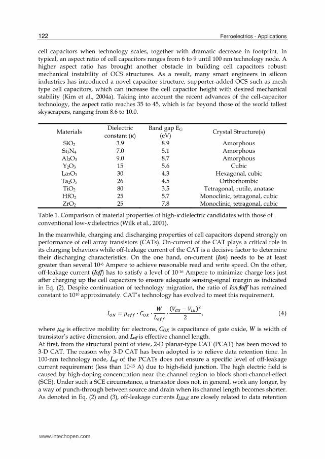
cell capacitors when technology scales, together with dramatic decrease in footprint. In typical, an aspect ratio of cell capacitors ranges from 6 to 9 until 100 nm technology node. A higher aspect ratio has brought another obstacle in building cell capacitors robust: mechanical instability of OCS structures. As a result, many smart engineers in silicon industries has introduced a novel capacitor structure, supporter-added OCS such as mesh type cell capacitors, which can increase the cell capacitor height with desired mechanical stability (Kim et al., 2004a). Taking into account the recent advances of the cell-capacitor technology, the aspect ratio reaches 35 to 45, which is far beyond those of the world tallest skyscrapers, ranging from 8.6 to 10.0.
Materials Dielectric
constant (κ) Band gap EG
(eV) Crystal Structure(s)
SiO2 3.9 8.9 Amorphous Si3N4 7.0 5.1 Amorphous Al2O3 9.0 8.7 Amorphous Y2O3 15 5.6 Cubic La2O3 30 4.3 Hexagonal, cubic Ta2O5 26 4.5 Orthorhombic TiO2 80 3.5 Tetragonal, rutile, anatase HfO2 25 5.7 Monoclinic, tetragonal, cubic ZrO2 25 7.8 Monoclinic, tetragonal, cubic
Table 1. Comparison of material properties of high-κ dielectric candidates with those of conventional low-κ dielectrics (Wilk et al., 2001).
In the meanwhile, charging and discharging properties of cell capacitors depend strongly on performance of cell array transistors (CATs). On-current of the CAT plays a critical role in its charging behaviors while off-leakage current of the CAT is a decisive factor to determine their discharging characteristics. On the one hand, on-current (Ion) needs to be at least greater than several 10-6 Ampere to achieve reasonable read and write speed. On the other, off-leakage current (Ioff) has to satisfy a level of 10-16 Ampere to minimize charge loss just after charging up the cell capacitors to ensure adequate sensing-signal margin as indicated in Eq. (2). Despite continuation of technology migration, the ratio of Ion/Ioff has remained constant to 1010 approximately. CAT’s technology has evolved to meet this requirement.
荊潮朝 噺 航勅捗捗 · 系潮諜 · 激詣勅捗捗 · 岫撃弔聴 伐 撃痛朕岻態に , 岫ね岻
where µeff is effective mobility for electrons, COX is capacitance of gate oxide, W is width of transistor’s active dimension, and Leff is effective channel length. At first, from the structural point of view, 2-D planar-type CAT (PCAT) has been moved to 3-D CAT. The reason why 3-D CAT has been adopted is to relieve data retention time. In 100-nm technology node, Leff of the PCATs does not ensure a specific level of off-leakage current requirement (less than 10-15 A) due to high-field junction. The high electric field is caused by high-doping concentration near the channel region to block short-channel-effect (SCE). Under such a SCE circumstance, a transistor does not, in general, work any longer, by a way of punch-through between source and drain when its channel length becomes shorter. As denoted in Eq. (2) and (3), off-leakage currents ILEAK are closely related to data retention
www.intechopen.com

Future Memory Technology and Ferroelectric Memory as an Ultimate Memory Solution 123
time. Generically this ILEAK arises from sub-threshold current and gate-induced drain leakage (GIDL) current of cell array transistors along with junction leakage current from storage node. As Leff is scaled down, the increased doping concentration against the SCE strengthens electric field across storage node junction. This increase in junction-leakage current results in degrading the data retention time (Kim et al., 1998). The degradation of data retention time becomes significant below 100 nm node due to rapid increase in junction electric field again (Kim & Jeong, 2005). This issue since the mid 2000’s has been overcome by introducing 3-D cell transistors, where the junction electric-field can be greatly reduced due to lightly doped channel. One example of these newly developed structures is RCAT (Recess Channel Array Transistor) structure whose channel detours around a part of silicon substrate so that the elongated channel can be embodied in the array transistor (Kim et al., 2003). Also, the RCAT structure gives us another benefit, which lessens threshold voltage (Vth) due to lower doping concentration. Thereby, not only does DRAM’s core circuitry operate at lower voltage but also CAT’s on-current increases, as denoted in Eq. (4). Note that, according to the Moore’s law, Vcc must be scaled down for power save. This trend has continued to come to 60 nm technology node. However, beyond 60 nm of technology node, on-current requirement has not been satisfied with such a RCAT approach alone. Thus, further innovations since 50 nm node have been pursued in a way of a negative word-line (NWL) scheme6 in DRAM core circuitry. The NWL scheme compared with a conventional ground-word-line (GWL) scheme, allows us Vth reduction further, which means more on-current. However, another adverse effect on the CAT can occur as a result of the NWL. Since CAT’s gate potential goes more negative during holding data stored at the storage junction, from which GIDL current increases as a function of gate-storage voltage, level of which is as high as that of gate potential compared with the conventional GWL. Many device engineers have given much effort to tackle this problem and finally have figured it out by technological implementation, for instance, mitigation of electric field exerted locally in the region overlapped between source/drain and gate in the RCAT. In pursuit of purpose, gate oxide needs to be different in thickness. Provided that the oxide thickness in the overlapped region is thicker than that in the channel, unwanted GIDL current will decrease in proportion to electric field of the overlapped zone in the storage-node to gate (Lee et al., 2008; Jung et al., 2009). According to our calculation, one can extend this NWL-based RCATs down to 40 nm node with minor modifications (Jung et al., 2009). In 30 nm technology node, it becomes extremely difficult to achieve the successful Ion/Ioff ratio. A report has shown that a body-tied FinFET (fin field-effect-transistor) as a cell array transistor seems to be very promising due to its superb performances: excellent immunity against the SCE; high trans-conductance; and small sub-threshold leakage (Lee et al., 2004). For example, it allows us to have not only lower Vth but lower sub-threshold swing due to a fin-gate structure, providing more width for on-current and wrapping the gate for Vth and sub-threshold swing down. It is believed that the body-tied FinFET leads DRAM technology to be extendable down to 30 nm node. In off-leakage current, CAT’s gate material has been being transformed to metal gate of higher work function (4.2~4.9 eV) instead of n+ poly-silicon gate. The lower Vth coming from higher work function provides us with lower channel doping. This leads to lower junction electric field and results in lower off-leakage 6Since a level of dc (direct current) bias at unselected word-lines is negative, sub-threshold leakage current of a cell transistor becomes extremely low because its channel has never chance to be on-set of inversion, leading to keeping a reasonable level of off-leakage current despite low Vth.
www.intechopen.com
Ferroelectrics - Applications 124
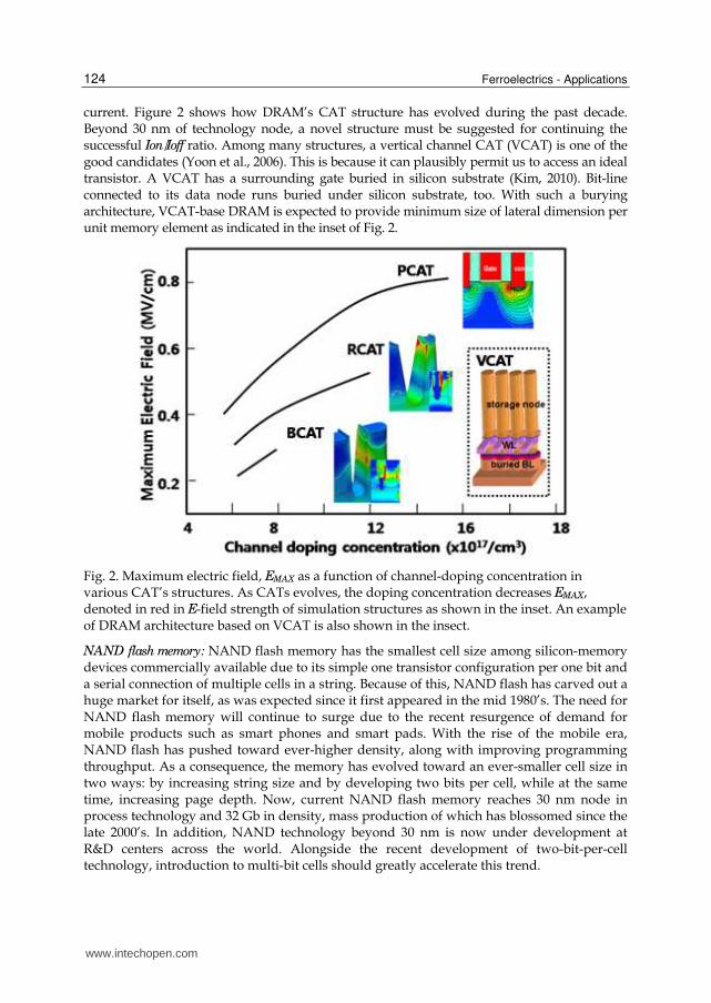
current. Figure 2 shows how DRAM’s CAT structure has evolved during the past decade. Beyond 30 nm of technology node, a novel structure must be suggested for continuing the successful Ion/Ioff ratio. Among many structures, a vertical channel CAT (VCAT) is one of the good candidates (Yoon et al., 2006). This is because it can plausibly permit us to access an ideal transistor. A VCAT has a surrounding gate buried in silicon substrate (Kim, 2010). Bit-line connected to its data node runs buried under silicon substrate, too. With such a burying architecture, VCAT-base DRAM is expected to provide minimum size of lateral dimension per unit memory element as indicated in the inset of Fig. 2.
Fig. 2. Maximum electric field, EMAX as a function of channel-doping concentration in various CAT’s structures. As CATs evolves, the doping concentration decreases EMAX, denoted in red in E-field strength of simulation structures as shown in the inset. An example of DRAM architecture based on VCAT is also shown in the insect.
NAND flash memory: NAND flash memory has the smallest cell size among silicon-memory devices commercially available due to its simple one transistor configuration per one bit and a serial connection of multiple cells in a string. Because of this, NAND flash has carved out a huge market for itself, as was expected since it first appeared in the mid 1980’s. The need for NAND flash memory will continue to surge due to the recent resurgence of demand for mobile products such as smart phones and smart pads. With the rise of the mobile era, NAND flash has pushed toward ever-higher density, along with improving programming throughput. As a consequence, the memory has evolved toward an ever-smaller cell size in two ways: by increasing string size and by developing two bits per cell, while at the same time, increasing page depth. Now, current NAND flash memory reaches 30 nm node in process technology and 32 Gb in density, mass production of which has blossomed since the late 2000’s. In addition, NAND technology beyond 30 nm is now under development at R&D centers across the world. Alongside the recent development of two-bit-per-cell technology, introduction to multi-bit cells should greatly accelerate this trend.
www.intechopen.com

Future Memory Technology and Ferroelectric Memory as an Ultimate Memory Solution 125
There are several prerequisite requirements to meet in terms of cell operation. Its cells must satisfy write and read constraints. First is programming disturbance. To program a cell, it is necessary to apply a certain amount of electric field across between floating gate and channel of the cell so that a sufficient amount of Fowler-Nordheim (FN) tunneling electrons can be injected into the floating gate.
な建潮諜 · 紘 · 撃牒弔暢 半 ~など 警結撃, 紘 噺 系寵聴系脹腸朝朝帳挑 髪 系寵聴 , 岫の岻
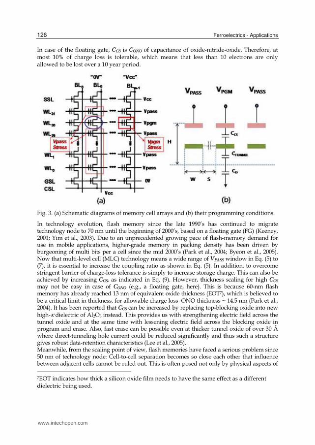
where tOX is thickness of tunnel oxide; γ is a coupling ratio; VPGM is programming voltage; CCS is capacitance between control gate and storage media; and CTUNNEL is capacitance of tunnel oxide. Figure 3 illustrates (a) a schematic diagram of NAND cell arrays and (b) their programming conditions. During the programming, there are two types of unselected cells that tolerate unwanted programming: One type is cells connected to the same bit-line of the selected cell. And the other is cells connected to the same word-line. The former suffers so called VPASS-stress cells while the latter endures so called VPGM-stress cells as follows:
撃牒凋聴聴 嫌建堅結嫌嫌 噺 な建潮諜 · 紘 · 撃牒凋聴聴 判 欠 血結拳 警結撃, 岫は岻
撃牒弔暢 嫌建堅結嫌嫌 噺 な建潮諜 · 紘 · 峪撃牒弔暢 伐 磐な 髪 系帖紘 · 系脹腸朝朝帳挑卑貸怠崋 判 欠 血結拳 警結撃, 岫ば岻
where VPASS stress is voltage applied to the unselected cells which share the same bit-line of the programming cell; VPGM stress is voltage applied to the unselected cells which share the same word-line; and CD is depletion capacitance of silicon substrate (See Fig. 3b). The VPASS-stress and the VPGM-stress are, in general, so small that neither electron injection into the unselected cells nor ejection from those is allowed in programming, respectively. Thus, VPASS window is determined by allowable both VPASS-stress and VPGM-stress. However, the VPASS window will be narrow when scaling down because of increase in depletion capacitance (CD) as denoted in Eq. (7). Thus, as technology scales, adequate VPASS window has to be satisfied. Next, in read operation, read voltage of a floating gate has to be higher than the highest threshold voltage of a cell string in order to pass read current through the string on which 32 cells are connected in series (in case of Fig. 3a). In similar to programming disturbance, read disturbance might occur in the unselected cells on the same string, and thus together with appropriate pass voltage, it is believed not only to choose tunnel oxide but to regulate its thickness in integration as well. 紘 · 撃眺帳凋帖 半 撃脹張 岫ぱ岻
As a rule of thumb, an adequate value of the coupling ratio in read lies in the range of 0.5 ~ 0.6, and reasonable thickness of the tunnel oxide is about 80 Å. Last but not least, one of the fundamental limitations of the NAND flash stems from the number of stored charge because the available number of storage electrons decreases rapidly with technology scaling. Provided that the voltage difference between the nearest states in a 2-level cell is less than 1 V, threshold voltage shifts due to charge loss will be restricted to less than 0.5 V, which puts the limitation on charge loss tolerance as follows, ∆芸 判 系寵聴 · ∆撃脹張 噺 ~ど.な芸, 岫ひ岻
www.intechopen.com
Ferroelectrics - Applications 126
In case of the floating gate, CCS is CONO of capacitance of oxide-nitride-oxide. Therefore, at most 10% of charge loss is tolerable, which means that less than 10 electrons are only allowed to be lost over a 10 year period.
Fig. 3. (a) Schematic diagrams of memory cell arrays and (b) their programming conditions.
In technology evolution, flash memory since the late 1990’s has continued to migrate technology node to 70 nm until the beginning of 2000’s, based on a floating gate (FG) (Keeney, 2001; Yim et al., 2003). Due to an unprecedented growing pace of flash-memory demand for use in mobile applications, higher-grade memory in packing density has been driven by burgeoning of multi bits per a cell since the mid 2000’s (Park et al., 2004; Byeon et al., 2005). Now that multi-level cell (MLC) technology means a wide range of VPASS window in Eq. (5) to (7), it is essential to increase the coupling ratio as shown in Eq. (5). In addition, to overcome stringent barrier of charge-loss tolerance is simply to increase storage charge. This can also be achieved by increasing CCS, as indicated in Eq. (9). However, thickness scaling for high CCS may not be easy in case of CONO (e.g., a floating gate, here). This is because 60-nm flash memory has already reached 13 nm of equivalent oxide thickness (EOT7), which is believed to be a critical limit in thickness, for allowable charge loss−ONO thickness ~ 14.5 nm (Park et al., 2004). It has been reported that CCS can be increased by replacing top-blocking oxide into new high-κ dielectric of Al2O3 instead. This provides us with strengthening electric field across the tunnel oxide and at the same time with lessening electric field across the blocking oxide in program and erase. Also, fast erase can be possible even at thicker tunnel oxide of over 30 Å where direct-tunneling hole current could be reduced significantly and thus such a structure gives robust data-retention characteristics (Lee et al., 2005). Meanwhile, from the scaling point of view, flash memories have faced a serious problem since 50 nm of technology node: Cell-to-cell separation becomes so close each other that influence between adjacent cells cannot be ruled out. This is often posed not only by physical aspects of 7EOT indicates how thick a silicon oxide film needs to have the same effect as a different dielectric being used.
www.intechopen.com

Future Memory Technology and Ferroelectric Memory as an Ultimate Memory Solution 127
cell structures but also by certain aspects of its performance. To circumvent cell-to-cell interference, width of a floating gate tends to be more aggressively squeezed than space between floating gates (See Fig. 3b). This seems to result in a high aspect ratio of a gate stack. Such a high aspect ratio can provoke fabrication difficulty of memory cells due to its mechanical instability. And stored charge (e.g., electron) in a floating gate can redistribute easily in operational conditions, leading to vulnerability of poor data retention. Since the interference originates from another type of coupling between floating gates (FGs), it is desirable to find innovative structures, where charge storage media do not have a form of continuum of charge like the floating gate style but have a discrete sort such as charge traps (CTs) in a nitride layer. The typical examples are non-volatile memories with non-floating gate, for example, SONOS (silicon-oxide-nitride-oxide-silicon) (Mori et al., 1991), SANOS (silicon-alumina-nitride-oxide-silicon) (Lee et al., 2005), TANOS (TaN-alumina-nitride-oxide-silicon) (Shin et al., 2006) or nano-crystal dots (Tiwari et al., 1995; Nakajima et al., 1998). Recently, 32 Gb flash memory has been reported, in particular, in 40 nm of technology node (Park et al., 2006). They have pioneered a novel structure with a high-κ dielectric of Al2O3 as the top oxide and TaN as a top electrode. With this approach, they can achieve several essential properties for NAND flash memory: reasonable programming/erasing characteristics, an adequate VPASS window for multi-bit operation and robust reliability. It is noteworthy that a TANOS structure has much better mechanical stability than that of an FG-type cell because of the far lower stack in height. Interference among TANOS cells hardly occurs due to nature of the charge trap mechanism−SiN (silicon nitride) traps act as point charges. This is the biggest advantage in CT-NAND flash memory. To scale NAND flash further down, we may need another cell technology. A FinFET could be a very promising candidate because it can increase storage electrons effectively by a way of expanding channel width of cell transistors, similar to 3-D CATs in DRAM. In this pursuit, a research group has successfully developed flash memory with a TANOS structure based on a 3-D, body-tied FinFET (Lee et al., 2006), where they can obtain excellent performance of NAND-flash cells with robust reliability. If there are much higher κ dielectrics than Al2O3, then we can further scale down the FinFET CT-NAND flash memory.
Fig. 4. (a) A schematic diagram of 3-D, body-tied FinFET NAND cells and (b) comparisons of the 3-D cells with 2-D, planar cells in threshold-voltage shift as a function of programmed threshold voltage, measured after suffering 5k program/erase cycles and a bake at 200 °C for 2 hours (Lee et al., 2006).
www.intechopen.com

Ferroelectrics - Applications 128
Figure 4 represents (a) a schematic diagram of 3-D, body-tied FinFET NAND cells and (b) comparisons of the 3-D cells with 2-D ones in threshold-voltage shift as a function of programmed threshold voltage, measured after suffering 5k program/erase cycles and a bake at 200 °C for 2 hours. The threshold-voltage delay has been improved to 0.32 V in 3-D NAND cells, compared with 2-D NAND ones.
2.2 Prospects of silicon technology As well aware that the era of 2-D, planar-based shrink technology is coming to an end, semiconductor institutes have seen enormous hurdles to overcome in order to keep up with the Moore’s doubling pace and thus to meet the requirements of highly demanding applications in mobile gadgetry. They have attempted to tackle those barriers by smart and versatile approaches of 3-D technology in integration hierarchy. One strand of the responses is to modify structures of elementary constituents such as DRAM’s CATs, its storage capacitors and storage transistors of flash memory to 3-D ones from the 2-D. A second thread revisits these modifications to a higher level of integration: memory stacking. And another move is to upgrade this into a system in a way of fusing of each device in functionality by utilizing smart CMOS technology, e.g., through-silicon-via (TSV).
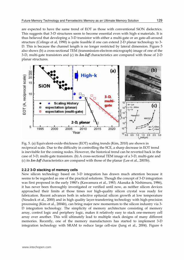
2.2.1 Elementary level of 3-D approach When working with silicon devices, a transistor’s key parameters must take into account: on-current; off-leakage current; the number of electrons contained in each transistor; or the number of transistors integrated. All of these factors are very important, but not equally important in functional features of silicon devices. For instance, for memory devices, off-leakage current is regarded as a more important factor and thus memory technologies tend to be developed with a greater emphasis on reducing off-leakage current. For logic, transistor delay is the single most important parameter, not just to indicate chip performance but to measure a level of excellence in device technology as well. This transistor delay is related closely to transistor’s on-current state. And with 2-D planar technology in logic, one can continue to reduce transistor’s channel length down to 40 nm. However, at less than 30 nm, the transistor begins to deviate in spite of a much relaxed off-current requirement. This is because of non-scalable physical parameters such as mobility, sub-threshold swing and parasitic resistance. To resolve these critical issues, two attempts have been examined. One is to enhance carrier mobility by using mobility-enhancement techniques such as strained silicon (Daembkes et al., 1986), SiGe/Ge channel (Ghani et al., 2003), or an ultra thin body of silicon (Hisamoto et al., 1989), where carrier scattering is suppressed effectively. Another approach is to reduce channel resistance by widening transistor’s width. In this case, it appears very promising to use different channel structures such as tri-gate (Chau et al., 2002) or multi channel (Lee et al., 2003b). We have witnessed that, with 3-D FinFETs in memory devices, this attempt is very efficient for extending incumbent shrink technology down to 30 nm of technology node. As silicon technology scales down further, the two will eventually be merged into one single solution for an optimum level of gate control. With this type of structure, one will arrive at nearly ideal transistor performance such as being virtually free from the SCE, sufficient on-current and suppressed off-leakage current. Figure 5 shows (a) evolution trends of logic transistors in terms of EOT: A sharp decrease in EOT trend appears due to lack of gate controllability in 2-D planar structures despite high-κ dielectrics. By contrast, those in 3-D, multi-gate structures
www.intechopen.com
Future Memory Technology and Ferroelectric Memory as an Ultimate Memory Solution 129
are expected to have the same trend of EOT as those with conventional SiON dielectrics. This suggests that 3-D structures seem to become essential even with high-κ materials. It is thus believed that developing a 3-D transistor with either a multi-gate or an gate-all-around structure (Colinge et al, 1990) is quite feasible if one can extend 2-D planar technology to 3-D. This is because the channel length is no longer restricted by lateral dimension. Figure 5 also shows (b) a cross-sectional TEM (transmission-electron-micrograph) image of one of the 3-D, multi-gate transistors and (c) its Ion-Ioff characteristics are compared with those of 2-D planar structures.
Fig. 5. (a) Equivalent-oxide-thickness (EOT) scaling trends (Kim, 2010) are shown in reciprocal scale. Due to the difficulty in controlling the SCE, a sharp decrease in EOT trend is inevitable for the coming nodes. However, the historical trend can be reverted back in the case of 3-D, multi-gate transistors. (b) A cross-sectional TEM image of a 3-D, multi-gate and (c) its Ion-Ioff characteristics are compared with those of the planar (Lee et al., 2003b).
2.2.2 3-D stacking of memory cells New silicon technology based on 3-D integration has drawn much attention because it seems to be regarded as one of the practical solutions. Though the concept of 3-D integration was first proposed in the early 1980’s (Kawamura et al., 1983; Akasaka & Nishimura, 1986), it has never been thoroughly investigated or verified until now, as neither silicon devices approached their limits at those times nor high-quality silicon crystal was ready for fabrication. Recent advances both in selective epitaxial silicon growth at low temperature (Neudeck et al., 2000) and in high quality layer-transferring technology with high-precision processing (Kim et al., 2004b), can bring major new momentum to the silicon industry via 3-D integration technology. The simplicity of memory architecture consisting of memory array, control logic and periphery logic, makes it relatively easy to stack one-memory cell array over another. This will ultimately lead to multiple stack designs of many different memories. Recently, one of the memory manufacturers has started to implement 3-D integration technology with SRAM to reduce large cell-size (Jung et al., 2004). Figure 6
www.intechopen.com

Ferroelectrics - Applications 130
shows (a) a cross-sectional TEM image of 3-D stacking SRAM (Left) and its schematic diagram (Right) (Jung et al., 2004): Since transistors stacked onto a given area do not need to isolate p-well to n-well, SRAM-cell size of 84 F2 is being reduced to the extremely small cell size of 25 F2. Encouraged by this successful approach, stacked flash memory has also been pursued. Figure 6 also represents (b) 3-D stacking NAND flash memory (Jung et al., 2006): This suggests great potential of 3-D memory stacking for large-scale use with 3-D flash-cell technology, which will spur further growth in high-density applications. Beyond 20 nm node, we believe that the most plausible way to increase density is to stack the cells vertically. Figure 6 displays (c) a 3-D schematic view of vertical NAND flash memory (Katamura et al., 2009), where SG is selecting gate, CG is control gate and PC is pipe connection. The stacking of memory cells via 3-D technology looms on the horizon, in particular, for NAND flash memory.
Fig. 6. (a) A cross-sectional TEM image of 3-D stacking SRAM (Left) and its schematic diagram (Right) (Jung et al., 2004). (b) 3-D stacking NAND flash memory (Jung et al., 2006). (c) A 3-D schematic view of vertical NAND flash memory (Katsumata et al., 2009), where SG is selecting gate; CG is control gate; and PC is pipe connection. (d) A cross-sectional SEM image of memory array after the removal of the sacrificial film (See Katsumata et al., 2009)
It is also believed that logic technology will shift to 3-D integration after a successful jumpstart in silicon business. The nature of a logic device, where transistors and interconnections are integrated as key elements, is not much different from those of stacked memory cells. It may be very advantageous to introduce 3-D integration technology to a logic area. Note that implementation of interconnection processes seems to be more efficient in vertical scale. For example, a dual or quad-core CPU can be realized with only a half or quarter of the chip size, which will result in significantly greater cost-effectiveness. Another promising use would be to improve logic performance by cutting down on the length of metallization. Decrease in interconnection length means a huge amount of reduction in parasitic RC components, i.e., a high speed and power saving. In addition, 3-D technology will make it easy to combine a memory device and a logic device onto one single chip
www.intechopen.com
Future Memory Technology and Ferroelectric Memory as an Ultimate Memory Solution 131
through hierarchical stacking. Since most parts of SoCs (system-on-chips) in the future will be allocated to memory, this combining trend will be accelerated. The next step will be to stack multi-functional electronics such as RF (radio frequency) modules, CISs (CMOS image sensors) and bio-sensors over the logic and memory layers.
2.2.3 Chip level of 3-D integration The early version of 3-D integration in chip level has been commercialized already in a multi-chip package (MCP), where each functional chip (not device) is stacked over one another and each chip is connected by wire bonding or through the ‘through-via hole’ bonding method within a single package. Figure 7 exhibits (a) a bird’s eyes view of multi-chip-package (MCP) by wire bonding; (b) wafer-level stack package with through-via-hole; (c) a photograph of 3-D integrated circuit; and (d) a schematic drawing of a 3-D device for use in medical applications. The advantages of the MCP are a small footprint and better performance compared to a discrete chip solution. It is expected that the MCP approach will continue to evolve. However, the fundamental limitation of MCP will be lack of cost-effectiveness due to a number of redundancy/repair requirements. In this respect, ‘through-
silicon-via’ (TSV) technology is able to overcome MCP limitations through an easy implementation of redundancies and repairs. Many groups have reported TSV-based integrated circuit (TSV IC), where a single integrated circuit is built by stacking silicon wafers or dies and interconnecting them vertically so that they can function as one single device (Topol et al., 2006; Arkalgud, 2009; Chen et al., 2009). In doing so, key technologies include TSV formation, wafer-thinning capability, thin wafer handling, wafers’ backside processes, and 3D-stacking processes (e.g., die-to-die, die-to-wafer and wafer-to-wafer). In detail, there are many challenging processes such as etching profiles of TSV sidewall, poor isolation liners and barrier-deposition profiles. All of these are likely to provoke TSV’s reliability concerns due to lack of protection from metal (e.g., Cu) contamination. A report of silicon-based TSV interposers (Rao et al., 2009) may have advantages over traditional PCB or ceramic substrate in that it has a shorter signal routing. This results from vertical interconnect and improved reliability due to similarity to silicon-based devices in thermal expansion and extreme miniaturization in volume. TSV-IC technologies together with the 3-D interposers will accelerate an adoption of 3-D system-in-package (SiP) with heterogeneous integration (See Fig. 7d). And this might be a next momentum for genuine 3D IC devices in the future because of tremendous benefits in footprint, performance, functionality, data bandwidth, and power. Besides, as the use of 3-D silicon technology has great potential to migrate today’s IT devices into a wide diversification of multi-functional gadgetry, it can also stimulate a trend that merges one technology with another, ranging from new materials through new devices to new concepts. In this regard, new materials may cover the followings: carbon nano-tube (CNT) (Iijima, 1991), nano-wire (NW) (Yanson et al., 1998), conducting polymer (Sirringhaus et al. 1998), and molecules (Collier et al., 1999). New devices could also be comprised of many active elements, such as tunneling transistors (Auer et al., 2001), spin transistors (Supriyo Datta & Biswajit Das, 1990), molecular transistors (Collier et al., 1999), single electron transistors (SETs) (Fulton & Dolan, 1987) and others. We may be able to extend this to new concepts, varying from nano-scale computing (DeHon, 2003) and FET decoding (Zhong et al., 2003) to lithography-free addressing (DeHon et al., 2003). To a certain extent, some of these will be readily integrated with 3-D silicon technologies. This integration will further enrich 3-D silicon technologies to create a variety of new multi-functional electronics, which will provide further substantive boosts to silicon industry, allowing us to make a projection of a nano-silicon era into practical realities tomorrow.
www.intechopen.com

Ferroelectrics - Applications 132
Fig. 7. (a) A bird’s eyes view of (a) multi-chip-package (MCP) by wire bonding. (b) Wafer-level stack package with through-via-hole. (c) A Photograph of 3-D integrated circuit. (d) A schematic drawing of a 3-D device for medical applications enabled by TSVs and silicon interposers.
These realities will be manifested in highly desirable applications of combining of information technology (IT), bio-technology (BT), and nano-technology (NT), to become so called fusion technology (FT). Given that key obstacles to realize this are tackled by bridging the gap between previously incompatible platforms in silicon-based CMOS technology and new technological concepts, a vast number of new applications will unfold. One example may be many applications related to health sensor technology, in particular, the early recognition of cancer diseases and the screening of harmful and poisonous elements pervasive in the environment. Further, when a nano-scale bio-transistor is available, lab-on-a-chip (LoC) will become a single solution integrating all of its essential components, such as micro-array, fluidics, sensors, scanners and displayers. Then, by its very nature8, one will have tons of benefits from a mass of disposable LoCs, which will stimulate the future silicon industry.
8As a successful booster for the silicon industry, whatever will be, it should be a high volume product at a reasonable price. PCs are high volume products, and hand-held phones are too. In that sense, LoC is very promising because its potential market is the entire population.
www.intechopen.com
Future Memory Technology and Ferroelectric Memory as an Ultimate Memory Solution 133
2.3 Remarks Not only do many challenges await silicon industries as technology enters the deep nano-dimension era but promising opportunities are also there. Equipped with new technologies such as 3-D scaling and a wealth of new materials, alongside fusing of related technologies, we will overcome many hurdles ahead and respond technological challenges we will stumble along the way. All plausible solutions described earlier tell us that planar-based technology will reach an impassable limit. 3-D technology begins to provide clear signs of serving as a foundation for a refuel of the silicon industry. The advantages of 3-D integration are numerous. They include: elimination of uncertainty in the electrical characteristics of deep nano-scale transistors; extendable use of silicon infrastructures, especially optical lithography tools; and formation of a baseline for multi-functional electronics and thus facilitation of implementing a hierarchical architecture, where each layer is dedicated to a specific functional purpose. Over the next decade, we will see great endeavors in numerous areas that will greatly stimulate the semiconductor business. Successful evolutions of device structures will continue and even accelerate at a greater pace in the not-too-distant future. In addition, device designs will converge onto a single mobile platform, covering many different capacities and services from telecommunication through broadcasting and a much higher degree of data processing. In line with this, silicon technology will still play a critical role in realizing functionally merged solutions. All of these will permit us to have invaluable clues not just on how to prepare future silicon technology but also on how to positively influence the entire silicon industry. This will allow us to attain an even more sophisticated fusing of technologies. As seen in the past, silicon technology will continue to provide our society with versatile solutions and as-yet unforeseen benefits in much more cost-effective ways.
3. Ferroelectric memory as an ultimate memory solution
3.1 Introduction There has been great interest to understand ferroelectric properties from the point of view of both fundamental physics and the need of nano-scale engineering for memory devices. On the one hand, since electric hysteresis in Rochelle salt was in 1920 discovered by Valasek (Valasek, 1921), there have been tremendous efforts to look through ferroelectricity in a comprehensive way over the past many decades. As a consequence, the phenomenological theory of ferroelectricity has been presented by many researchers: Devonshire (Devonshire, 1949; Devonshire, 1951); Jona and Shirane (Jona and Shirane, 1962); Fatuzzo and Merz (Fatuzzo and Merz, 1959); Line and Glass (Line and Glass, 1979); and Haun (Haun, 1988). The series of their works have been successful to express the internal energy of a ferroelectric crystal system. This theory has also been examined experimentally in detail, and extended by Merz (Merz, 1953); by Drougard et. al. (Drougard et al., 1955); and by Triebwasser (Triebwasser, 1956). Especially, Devonshire’s phenomenological theory (Devonshire, 1949; Devonshire, 1951) gives the free energy of BaTiO3 as a function of polarization and temperature. From this free energy we know what the possible state and meta-stable states of polarization are in the absence of an applied field. We also know how polarization changes as a function of field applied to the crystal. In short, according to the theory, a ferroelectric possesses two minima (e.g., a second-order phase transition) in the internal energy. These two minima are separated by an energy barrier ΔE. Essential feature of a ferroelectric is that these two minima corresponds to two different spontaneous
www.intechopen.com

Ferroelectrics - Applications 134
polarizations that can be changeable reversibly by an applied field. Under an assumption that applied electric field is able to surmount the energy barrier, the advent of smart thin-film technology in evolution of CMOS technology, has enabled to consider a ferroelectric crystal a useful application. Thinning a ferroelectric film with high purity means that there could be an opportunity to use ferroelectrics as a memory element. On the other, integrated ferroelectrics are a subject of considerable research efforts because of their potential applications as an ultimate memory device due to 3 reasons: First, the capability of ferroelectric materials to sustain an electrical polarization in the absence of an applied field, means that integrated ferroelectric capacitors are non-volatile. They can retain information over a long period of time without a power supply. Second, the similar architectural configuration of memory cell-array to conventional ones, means that they are highly capable of processing massive amounts of data. Finally, nano-second speed of domain switching implies that they are applicable to a high-speed memory device. Since ferroelectric capacitors was explored for use in memory applications by Kinney et al. (Kinney et al., 1987); Evans and Womack (Evans & Womack, 1988); and Eaton et al. (Eaton et al., 1988), it has been attempted to epitomize ferroelectrics to applicable memory solutions in many aspects. In the beginning of 1990’s, silicon institutes have begun to exploit ferroelectrics as an application for high-density DRAMs (Moazzami et al., 1992; Ohno et al., 1994). This is because permittivity of ferroelectrics is so high as to achieve DRAM’s capacitance extremely high and thus appropriate for high density DRAMs. An early version of non-volatile ferroelectric RAM (random-access-memory) used to be several kilo bits in packing density. This lower density (NB. at that moment, DRAM had several ten mega bits in density) is because of two: One is that its memory unit was relatively large in size, being comprised of two transistors and two capacitors (2T2C) to maximize sensing signal. The other is that a ferroelectric capacitor stack has required not only novel metal electrodes such as platinum, iridium and rhodium, all of which are hard to be fine-patterned due to processing hardness, but also reluctant metal-oxide materials to conventional CMOS integration due to possible cross contaminants such as lead zircornate titanate (PbZrTiO3) and strontium bismuth titanate (Sr1-xBixTiO3). Next steps for high density non-volatile memory have been forwarded (Tanabe et al., 1995; Sumi et al., 1995; Song et al., 1999). In similar to DRAM, an attempt to build smaller unit cell in size was in the late 1990’s that one transistor and one capacitor (1T1C) per unit memory was developed (Jung et al., 1998). Since then, many efforts to build high density FRAM have been pursued, leading to several ten mega bits in density during the 2000s (Lee et al., 1999; Kim et al., 2002; Kang et al., 2006; Hong et al., 2007; Jung et. al, 2008).
Fig. 8. (a) Evolution of electronic components in data throughput performance. (b) NVM (non-volatile memory) filling price/performance gap.
www.intechopen.com

Future Memory Technology and Ferroelectric Memory as an Ultimate Memory Solution 135
Among integrated ferroelectrics, one of the most important parameters in FRAM is sensing signal margin. The sensing signal of FRAM is proportional to remanent polarization (Pr) of a ferroelectric capacitor as follows:
∆撃喋挑 噺 に鶏追畦系喋挑 噺 に香待香畦系喋挑穴 , 岫など岻
where A is capacitor’s area; d is capacitor’s thickness. As seen in equation (10), in principle, we have to compensate the area reduction when technology scales down. However, in practice, when the thickness of PZT ferroelectric thin film decreases, degradation of polarization tends to appear in the ferroelectric capacitor due to a dead layer between the ferroelectric and electrodes (See section 3.3.3). Unlike the requirement of DRAM’s CAT, the array transistor of FRAM is not necessarily constrained from the off-leakage current due to no need of the refresh cycles, but from on-current, which is at least greater than several µA in order for a reasonable read and write speed. Thus, this will greatly relieve technology scaling quandaries and enable fast technology migration to the high end. This is because designing of a less leaky cell transistor becomes very difficult in incumbent memories such as DRAM and NAND/NOR flash due to need of lower doping concentration. As witnessed in the Moore’s law, there has been enormous improvement in VLSI (very large-scale integration) technology to implement system performance of computing platforms in many ways over the past decades. For instance, data throughput of central processing unit (CPU) has been increased by thousand times faster than that of Intel 286TM emerged in the beginning of 1980’s. Alongside, a latest version of DRAM reaches a clock speed of more than 1 GHz. By contrast, state-of-the-art HDD (hard disk drive) transfers data at 600 MB/sec around (See Fig. 8a). Note that data rate of the latest HDD is still orders of magnitude slower than the processor/system-memory clock speed (see Fig. 8b). To achieve the throughput performance in more effective way, it is therefore needed to bridge performance gap in between each component. To compensate the gap between CPU and system memory, a CPU cache9 has been required and adopted. In line with this, ferroelectric memory is non-volatile, high-speed. But it has a destructive read-out scheme in core circuitry, whose memory cells need to return the original state after being read. This is because the original information is destroyed after read. As a result, it is essential to return the information back to its original state, which is so-called restore, necessarily following the read. This operation is so inevitable in the destructive read-out memory such as DRAM and FRAM. In particular, when the ferroelectric memory are used as one of the storage devices in computing system, such as a byte-addressable non-volatile (NV)-cache device, the memory has to ensure lifetime endurance, which is regarded as the number of read/write (or erase if such operation is required) cycles that memory can withstand before loss of any of entire bit information. Thus, authors are here trying to attempt not only how FRAM provides NV-cache solutions in a multimedia storage system such as solid state disk (SSD) with performance benefits but also what should be satisfied in terms of lifetime data-retention and endurance in such applications. Here, we also put forward size effect of ferroelectric film in terms of temperature-dependent dielectric anomaly because a dead layer plays an adverse role in thickness scaling. In addition, it is very important to ensure that integration technology of FRAM in nano-dimension is extendable to one of the 9File system cache is an area of physical memory that stores recently used data as long as possible to permit access to the data without having read from the disk.
www.intechopen.com
Ferroelectrics - Applications 136
conventional memories. Accordingly, we will present key integration technologies for ferroelectric memory to become highly mass-productive, highly reliable and highly scalable. This covers etching technology to provide a fine-patterned cell with less damage from plasma treatments; stack technology to build a robust ferroelectric cell capacitor; encapsulation technology to protect the ferroelectric cell capacitors from process integration afterwards; and vertical conjunction technology onto ferroelectric cell capacitors for multi-level metallization processes.
3.2 Non-volatile RAM as an ultimate memory solution
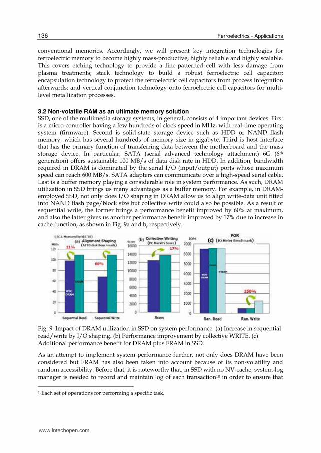
SSD, one of the multimedia storage systems, in general, consists of 4 important devices. First is a micro-controller having a few hundreds of clock speed in MHz, with real-time operating system (firmware). Second is solid-state storage device such as HDD or NAND flash memory, which has several hundreds of memory size in gigabyte. Third is host interface that has the primary function of transferring data between the motherboard and the mass storage device. In particular, SATA (serial advanced technology attachment) 6G (6th generation) offers sustainable 100 MB/s of data disk rate in HDD. In addition, bandwidth required in DRAM is dominated by the serial I/O (input/output) ports whose maximum speed can reach 600 MB/s. SATA adapters can communicate over a high-speed serial cable. Last is a buffer memory playing a considerable role in system performance. As such, DRAM utilization in SSD brings us many advantages as a buffer memory. For example, in DRAM-employed SSD, not only does I/O shaping in DRAM allow us to align write-data unit fitted into NAND flash page/block size but collective write could also be possible. As a result of sequential write, the former brings a performance benefit improved by 60% at maximum, and also the latter gives us another performance benefit improved by 17% due to increase in cache function, as shown in Fig. 9a and b, respectively.
Fig. 9. Impact of DRAM utilization in SSD on system performance. (a) Increase in sequential read/write by I/O shaping. (b) Performance improvement by collective WRITE. (c) Additional performance benefit for DRAM plus FRAM in SSD.
As an attempt to implement system performance further, not only does DRAM have been considered but FRAM has also been taken into account because of its non-volatility and random accessibility. Before that, it is noteworthy that, in SSD with no NV-cache, system-log manager is needed to record and maintain log of each transaction10 in order to ensure that 10Each set of operations for performing a specific task.
www.intechopen.com

Future Memory Technology and Ferroelectric Memory as an Ultimate Memory Solution 137
file system maintains consistency even during a power-failure. A log file that contains all the changes in metadata, generally serves as a history list of transactions performed by the file system over a certain period of time. Once the changes are recorded to this log, the actual operation is now executed. This is so-called power-off recovery (POR). By contrast, POR is redundant in FRAM-employed-SSD as a NV-cache because metadata can be protected by FRAM. Elimination of POR overhead is the single most critical implementation by utilization of FRAM. This is because FRAM provides such system with byte-addressable and non-volatile RAM function. Thus, in spite of sudden power failure, system can safely be protected by adopting FRAM even without POR overhead, ensuring integrity of metadata stored in the ferroelectric memory. Through many benchmark tools, we have confirmed that by eliminating this overhead, system performance has been increased by 250% in random write (See Fig. 9c). This also brings the system to no need of flush operation in file system. As a consequence, additional 9.4% increase in performance, maximizing cache-hitting ratio. Since metadata frequently updated do not necessarily go to NAND flash medium, endurance of the flash memories can be increased by 8% at maximum as well. Besides, failure rate of operations can be reduced by 20% due to firmware robustness increased mostly by elimination of the POR overhead.
Fig. 10. Data locality of FRAM as a code memory.
Meanwhile, how many endurance cycles are necessary for use in applications of NV-cache solutions such as data memory and code memory? To answer this question, we need to understand access patterns of NV-cache devices in multimedia system. Now, we take into account the followings: First is the ratio of read/write per cycle in data memory (likewise, number of data fetching per cycle in code memory). Generally, the ratio for data memory and code memory is 1.00 and 0.75, respectively. Second is data locality11. Figure 10 is a simulation result showing strong locality of 1.5% when FRAM has been considered a code 11The locality of reference is the phenomenon that the collection of data locations often consists of relatively well predictable clusters of code space in bytes.
www.intechopen.com

Ferroelectrics - Applications 138
memory. As shown in Fig. 10, less than 200 bytes of code space is more frequently accessed. Provided wear-leveling in read/write against the strong locality and taking an example of 20 MHz clock frequency of main memory (CPU clock ~ 200 MHz), what has been found is that the endurance cycles for 10-year lifetime becomes less than 9.5 × 10¹³. This number of cycles is far less than the cycles we presumably assumed, which is more than 1015 cycles. Thus, authors believe that more than 1.0 × 10¹⁴ of the endurance cycles is big enough to ensure that the ferroelectric memory as a NV-cache is so endurance-free as to be adopted to a multimedia storage system.
3.3 Reliabilities 3.3.1 Retention Since Merz’s exploration of domain switching kinetics in the mid 1950’s (Merz, 1954), it is now believed that polarization reversal occurs in a way of domain nucleation and growth (Landauer, 1957; Pulavari & Kluebler, 1958; Key & Dunn, 1962; Du & Chen, 1997; Jung et al., 2002; Kim et al., 2005; Jo et al., 2006). The retention time of FRAM is closely related to a decay rate of the polarization reversal of a ferroelectric capacitor as expressed in formula (11).
Fig. 11. (a) A decay exponent n plot against estimated thermal energy ΔF*/kBT in various thickness of of BaTiO3 films and (b) thermal energy barrier ΔF*/kBT as a function of thickness in different ferroelectric stacks.
鶏岫建岻鶏待 噺 磐 建建待卑貸津 岫なな岻
∆繋茅 噺 伐に継鶏聴撃 髪 購栂畦 髪 戟鳥 岫なに岻
where P0 is initial remanent polarization; P(t) is remanent polarization at time t; t0 is a time constant; n is an exponent; ∆繋茅 is domain free energy; E is homogeneous electric field applied externally; V is the volume of domain nucleus; σw is domain wall energy; A is domain wall area. While the first term of Eq. (12) represents the electrostatic energy gained by formation of a domain nucleus, the second is the surface energy, and the last term is the field energy of the depolarizing field (Merz, 1954). Provided that length of domain nuclei is much smaller than thickness of a ferroelectric, half-prolate spheroidal nuclei tends to be formed and finally reaches a cylindrical shape (Key & Dunn, 1962; Jung et al., 2002). Under such an assumption, if one can measure depolarization energy of Eq. (12), we can now
www.intechopen.com

Future Memory Technology and Ferroelectric Memory as an Ultimate Memory Solution 139
estimate ∆繋茅/倦喋劇, where kB is Boltzmann constant. Based on experimental values of depolarization field Ed that ranges from 300 to 800 kV/cm (Kim et al., 2005), the corresponding ∆繋茅/倦喋劇 is estimated to 4 to 20 at ambient temperature (Jo et al., 2006). Figure 11 represents (a) a decay exponent n plot against estimated thermal energy ΔF*/kBT in various thickness of BaTiO3 films and (b) thermal energy barrier ΔF*/kBT as a function of thickness in different ferroelectric stacks. As seen in Fig. 11a, in most of interesting nano-ferroelectrics with thickness ranging from 5 to 30 nm, the energy barrier is evaluated to ΔF*/kBT ~ 150 kBT for n ~ 0.017, which is the exponent corresponding to 50% of polarization decay during 10 years in Eq. (11). Thus, as shown in Fig. 11b, if one takes into account a stack of SrRuO3-PbTiO3-SrRuO3 (SRO-PTO-SRO), the energy barrier of polarization reversal via the formation of domain nuclei during 10 years is more than 150 kBT, which means that there is virtually no retention conumdrum in FRAM as long as a ferroelectric stack is properly chosen.
3.3.2 Endurance In FRAM, it is not readily achieved to assure whether or not a memory device can endure virtually infinite read/write cycles. This is because of memory size that is several tens or hundreds megabits typically. For instance, a HTOL (high temperature operational life) test during 2 weeks at 125 oC, is merely a few millions of endurance cycles for each memory cell in 64-Mb memory size, for example. Even taking into account minimum number of cells (in this case 128 bits because of 16 I/Os), time to take evaluation of 1013 cycles is at least more than 20 days. Therefore, it is essential to find acceleration factors to estimate device endurance through measurable quantities such as voltage and temperature. However, direct extraction of acceleration factors from memory chips is not as easy in practice as it seems to be in theory. This is because VLSI circuit consists of many discrete CMOS components that have a temperature and voltage range to work. Generally, more than 125 oC is supposed to be a limit to operate properly. A voltage range of a memory device is also specified in given technology node (±10% of VDD=1.8 V in this case). Despite those difficulties, it has been attempted to figure out acceleration factors in terms of temperature and voltage, together with information obtained from capacitor-level tests. In regard to package-level endurance, figure 12 represents changes in (a) peak-to-peak sensing margin (SMpp) and (b) tail-to-tail sensing margin (SMtt) as read/write cycles continues to stress devices cumulatively at 125 oC. Both SMpp and SMtt have been obtained by averaging out 30 package samples for each stress voltage. Function-failed packages have been observed when SMpp and SMtt reach 10% and 25% loss of each initial value, respectively. As seen in Fig. 12a and b, voltage acceleration factors (AFV) between 2.0 V and 2.5 V has been calculated by these criteria (AFV = 81 at SMpp and AFV = 665 at SMtt). In other words, the test FRAMs can endure 1 × 10¹² of read/write cycles at the condition of 125 oC and 2.0 V. Second, in capacitor-level endurance, figure 13 is (a) a normalized polarization plot against cumulative fatigue cycles at 145 oC in a variable voltage range and (b) a logarithm plot of cycle-to-failure (CTF) as a function of stress voltage in a various range of temperature. Here, we introduce a term of CTF which is referred to as an endurance cycle at which remanent polarization (or sensing margin) has a reasonable value for cell capacitors (or memory) to operate. Polarization drops gradually as fatigue cycles increase and the collapsing rate is accelerated as stress voltage goes higher. Likewise, provided 10% loss of polarization is criteria of CTF, the CTF at 145 oC and 2.0 V approximates 2.2 × 10¹². (NB. This
www.intechopen.com

Ferroelectrics - Applications 140
is reasonable because samples of 10% loss in SMpp turned out to be defective functionally.) Considering temperature- and voltage-acceleration factors from Fig. 13a, acceleration condition of 145 oC, 3.5V is more stressful in 5 orders of magnitude than that of 85 oC, 2.0 V. In other words, 1.0 × 10⁹ of CTF at 145 oC, 3.5 V is equivalent to 6.0 × 10¹⁴ at 85 oC, 2.0 V.
Fig. 12. Changes in (a) peak-to-peak sensing margin (SMpp) and (b) tail-to-tail sensing margin (SMtt) as a function of endurance cycles at 125 oC. (c) SMpp vs. endurance cycles at 125 oC, 2.5 V. (d) SMtt vs. endurance cycles at 125 oC, 2.5 V. SMt and SMi of the ordinate in Fig. 12a and b is sensing margin at time t and initial time, respectively.
Results of the acceleration factors obtained from device-level tests differ from those in capacitor-level. For example, while AFV(2.5 V/2.0 V) of 81 in device-level tests12, that of 16 in capacitor-level. We have yet to find a reasonable clue of what makes this difference. But it could be thought that the difference might arise from the fact that a memory device contains many different functional circuitries such as voltage-latch sense amplifiers, word-line/plate-line drivers, all of which make tiny amount of voltage difference magnify each effect on cell capacitors. This tendency can also be observed in the big gap of AFV obtained from two different definitions between SMtt (AFV = 665) and SMpp (AFV = 81). Tail-bit behaviors of memory cells could include a certain amount of extrinsic imperfection, in general. Thus, we believe that results tested in capacitor-level seem to be close to a fundamental nature of CTF 12It is thought that AFV in capacitor-level tests follows AFV of SMpp in device-level rather than that of SMtt because of nature of capacitor-level tests that average out all the cell capacitor connected in parallel.
www.intechopen.com

Future Memory Technology and Ferroelectric Memory as an Ultimate Memory Solution 141
than those in device-level tests due to lack of extrinsic components. Figure 14 is (a) a logarithm plot of CTF as stress voltage increases in a various range of temperature and (b) Weibull distribution of endurance life in package samples tested at 125 oC in a various voltage range. The distributions in a 2.2-3.0 V range of voltage have a similar shape parameter, m~2.4. This suggests that evaluation of endurance tests in device-level makes sense in physical term. As seen in Fig. 14a, voltage-endurance stress at less than 2.0 V does not allow us to obtain any sign of degradation in sensing margins within a measurable time span. Nor does temperature-endurance stress above 125 oC due to off-limits of operational specifications of the device.
Fig. 13. (a) A normalized polarization plot against cumulative fatigue cycles at 145 oC in a variable voltage range. (b) Logarithm of CTF vs. stress voltage, VDD at 145 oC.
Fig. 14. (a) A logarithm plot of CTF as stress voltage increases in a various range of temperature and (b) distributions of endurance life in device-level tests at 125 oC.
3.3.3 Temperature-dependent dielectric anomaly Since ferroelectricity involves the cooperative alignment of electric dipoles responding external field applied, there should be a critical volume below which the total energy associated with domain nucleation and growth, is outweighed by the entropic desire to
www.intechopen.com
Ferroelectrics - Applications 142
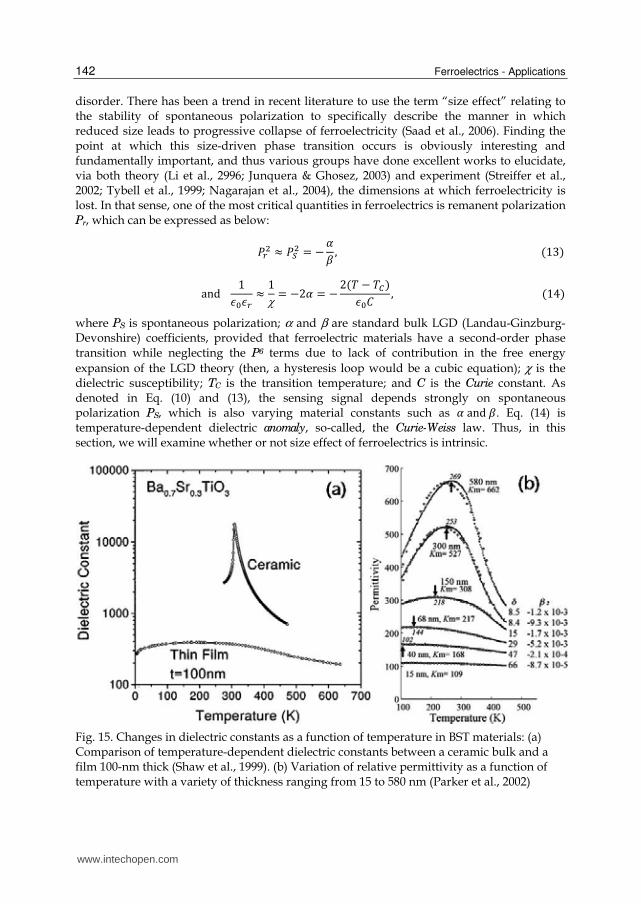
disorder. There has been a trend in recent literature to use the term “size effect” relating to the stability of spontaneous polarization to specifically describe the manner in which reduced size leads to progressive collapse of ferroelectricity (Saad et al., 2006). Finding the point at which this size-driven phase transition occurs is obviously interesting and fundamentally important, and thus various groups have done excellent works to elucidate, via both theory (Li et al., 2996; Junquera & Ghosez, 2003) and experiment (Streiffer et al., 2002; Tybell et al., 1999; Nagarajan et al., 2004), the dimensions at which ferroelectricity is lost. In that sense, one of the most critical quantities in ferroelectrics is remanent polarization Pr, which can be expressed as below: 鶏追態 蛤 鶏聴態 噺 伐 糠紅 , 岫なぬ岻
and な香待香追 蛤 なχ 噺 伐に糠 噺 伐 に岫劇 伐 劇寵岻香待系 , 岫なね岻
where PS is spontaneous polarization; α and β are standard bulk LGD (Landau-Ginzburg-Devonshire) coefficients, provided that ferroelectric materials have a second-order phase transition while neglecting the P6 terms due to lack of contribution in the free energy expansion of the LGD theory (then, a hysteresis loop would be a cubic equation); χ is the dielectric susceptibility; TC is the transition temperature; and C is the Curie constant. As denoted in Eq. (10) and (13), the sensing signal depends strongly on spontaneous polarization PS, which is also varying material constants such as 糠 and 紅. Eq. (14) is temperature-dependent dielectric anomaly, so-called, the Curie-Weiss law. Thus, in this section, we will examine whether or not size effect of ferroelectrics is intrinsic.
Fig. 15. Changes in dielectric constants as a function of temperature in BST materials: (a) Comparison of temperature-dependent dielectric constants between a ceramic bulk and a film 100-nm thick (Shaw et al., 1999). (b) Variation of relative permittivity as a function of temperature with a variety of thickness ranging from 15 to 580 nm (Parker et al., 2002)
www.intechopen.com
Future Memory Technology and Ferroelectric Memory as an Ultimate Memory Solution 143
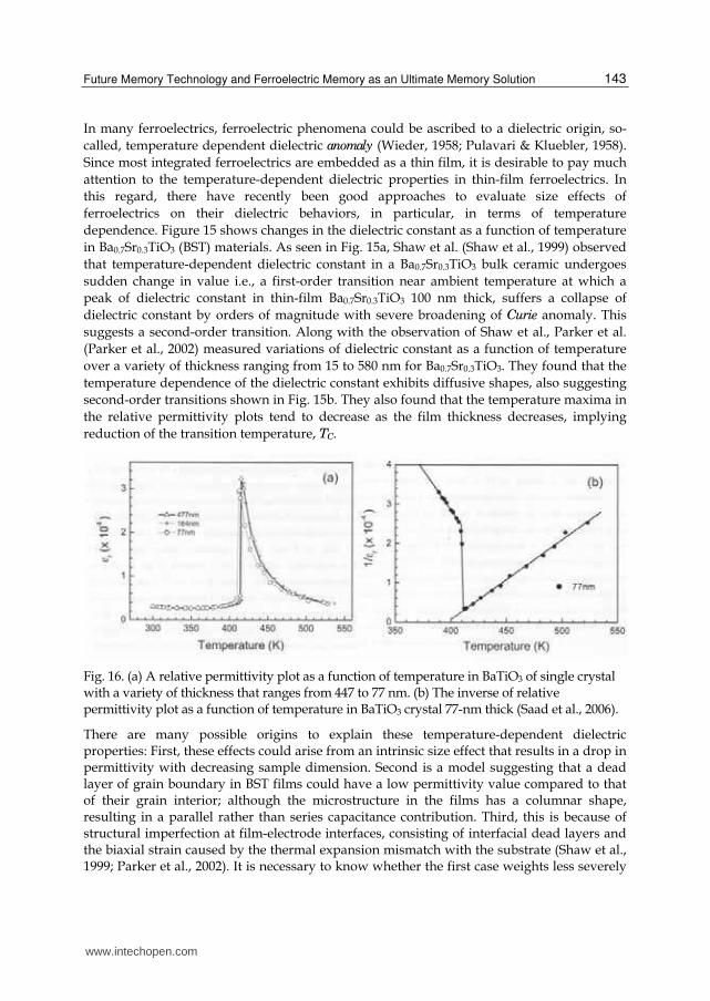
In many ferroelectrics, ferroelectric phenomena could be ascribed to a dielectric origin, so-called, temperature dependent dielectric anomaly (Wieder, 1958; Pulavari & Kluebler, 1958). Since most integrated ferroelectrics are embedded as a thin film, it is desirable to pay much attention to the temperature-dependent dielectric properties in thin-film ferroelectrics. In this regard, there have recently been good approaches to evaluate size effects of ferroelectrics on their dielectric behaviors, in particular, in terms of temperature dependence. Figure 15 shows changes in the dielectric constant as a function of temperature in Ba0.7Sr0.3TiO3 (BST) materials. As seen in Fig. 15a, Shaw et al. (Shaw et al., 1999) observed that temperature-dependent dielectric constant in a Ba0.7Sr0.3TiO3 bulk ceramic undergoes sudden change in value i.e., a first-order transition near ambient temperature at which a peak of dielectric constant in thin-film Ba0.7Sr0.3TiO3 100 nm thick, suffers a collapse of dielectric constant by orders of magnitude with severe broadening of Curie anomaly. This suggests a second-order transition. Along with the observation of Shaw et al., Parker et al. (Parker et al., 2002) measured variations of dielectric constant as a function of temperature over a variety of thickness ranging from 15 to 580 nm for Ba0.7Sr0.3TiO3. They found that the temperature dependence of the dielectric constant exhibits diffusive shapes, also suggesting second-order transitions shown in Fig. 15b. They also found that the temperature maxima in the relative permittivity plots tend to decrease as the film thickness decreases, implying reduction of the transition temperature, TC.
Fig. 16. (a) A relative permittivity plot as a function of temperature in BaTiO3 of single crystal with a variety of thickness that ranges from 447 to 77 nm. (b) The inverse of relative permittivity plot as a function of temperature in BaTiO3 crystal 77-nm thick (Saad et al., 2006).
There are many possible origins to explain these temperature-dependent dielectric properties: First, these effects could arise from an intrinsic size effect that results in a drop in permittivity with decreasing sample dimension. Second is a model suggesting that a dead layer of grain boundary in BST films could have a low permittivity value compared to that of their grain interior; although the microstructure in the films has a columnar shape, resulting in a parallel rather than series capacitance contribution. Third, this is because of structural imperfection at film-electrode interfaces, consisting of interfacial dead layers and the biaxial strain caused by the thermal expansion mismatch with the substrate (Shaw et al., 1999; Parker et al., 2002). It is necessary to know whether the first case weights less severely
www.intechopen.com
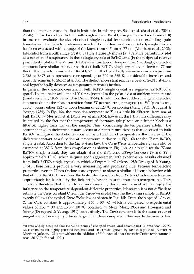
Ferroelectrics - Applications 144
than the others, because the first is instrinsic. In this respect, Saad et al. (Saad et al., 2004a, 2004b) devised a method to thin bulk single-crystal BaTiO3 using a focused ion beam (FIB) in order to evaluate the size effects of single crystal ferroelectrics thus excluding grain boundaries. The dielectric behaviors as a function of temperature in BaTiO3 single crystals has been evaluated with a range of thickness from 447 nm to 77 nm (Morrison et al., 2005), fabricated from a bulk single crystal BaTiO3. Figure 16 shows (a) a relative permittivity plot as a function of temperature in these single crystals of BaTiO3 and (b) the reciprocal relative permittivity plot of the 77 nm BaTiO3 as a function of temperature. Startlingly, dielectric constants have similar behavior to that of bulk BaTiO3 single crystal even down to 77 nm thick. The dielectric constant in BaTiO3 77 nm thick gradually decrease over a range from 2,738 to 2,478 at temperature corresponding to 300 to 365 K, considerably increases and abruptly soars up to 26,663 at 410 K. The dielectric constant reaches a peak of 26,910 at 413 K and hyperbolically dcreases as temperature increases further. In general, the dielectric constant in bulk BaTiO3 single crystal are regarded as 160 for 香c (parallel to the polar axis) and 4100 for 香a (normal to the polar axis) at ambient temperature (Landauer et al., 1956; Benedict & Duran, 1958). In addition, the sudden change in dielectric constants due to the phase transition from FT (ferroelectric, tetragonal) to PC (paraelectric, cubic), occurs either 122 oC upon heating or at 120 oC on cooling (Merz, 1953; Drougard & Young, 1954). In Fig. 16a, the transition temperature TC is a little bit different from one of bulk BaTiO3.13 Morrison et al. (Morrison et al., 2005), however, think that this difference may be caused by the fact that the temperature of thermocouple placed on a heater block is a little bit higher than that on the sample. Thus, considering the temperature artefact, the abrupt change in dielectric constant occurs at a temperature close to that observed in bulk BaTiO3. Alongside the dielectric constant as a function of temperature, the inverse of the dielectric constant as a function of temperature is shown in Fig. 16b for the 77-nm BaTiO3 single crystal. According to the Curie-Weiss law, the Curie-Weiss temperature T0 can also be estimated at 382 K from the extrapolation as shown in Fig. 16b. As a result, for the 77-nm BaTiO3 single crystal, they can obtain that the difference ΔTemp between TC and T0 is approximately 13 oC, which is quite good aggreeement wth experimental results obtained from bulk BaTiO3 single crystal, in which ΔTemp = 14 oC (Merz, 1953; Drougard & Young, 1954). These results provide a very intersesting and promising clue, because ferroelectric properties even in 77-nm thickness are expected to show a similar dielectric behavior with that of bulk BaTiO3. In addition, the first-order transition from FT to PC in ferroelectrics can appropriately be decribed by the dielectric behaviors near the transition temepertures. They conclude therefore that, down to 77 nm dimension, the intrinsic size effect has negligible influence on the temperature-dependent dielectric properties. Moreover, it is not difficult to estimate the Curie constant C from the Curie-Weiss plot because the 77-nm sample of BaTiO3 exactly follows the typical Curie-Weiss law as shown in Fig. 16b. From the slope of 1/ 香r vs. T, the Curie constant is approximately 4.53 × 10⁵ oC, which is compared to experimental values of 1.56 × 10⁵ and 1.73 × 10⁵ oC, obtained by Merz (Merz, 1953) and Drougard and Young (Drougard & Young, 1954), respectively. The Curie constant is in the same order of magnitude but is roughly 3 times larger than those compared. This may be because of two 13It was widely accepted that the Curie point of undoped crystal and ceramic BaTiO3 was near 120 ºC. Measurements on highly purified ceramics and on crystals grown by Remica’s process (Remica & Morrison Jackson, 1954) but without the addition of Fe3+ have shown that their Curies temperature is near 130 ºC (Jaffe et al., 1971).
www.intechopen.com
Future Memory Technology and Ferroelectric Memory as an Ultimate Memory Solution 145
factors: Errors in electrode area and thickness can affect the Curie constant dramatically; and the temperature difference between sample and thermocouple may not be constant.
3.4 Key technologies Etching damage: It is widely accepted that as a device shrinks, node separation of cell capacitors is not readily achievable due to necessity of novel metals that served as electrodes of the MIM (Metal-Insulaor-Metal) cell capacitor, such as iridium, iridium oxide, strontium ruthenium oxide (SrRuO3). In typical, remanent polarization depends heavily on processing temperature at which ferroelectric PZT (PbZr0.4Ti0.6O3) is etched. The remanent polarization (Pr) value drops drastically as temperature of the processing chuck in an etching chamber increases. According to a report of etching impact on ferroelectrics (Jung et al., 2007), there is no direct evidence how higher-temperature etching makes a Pr value smaller. But it is believed that a certain amount of halides or halide ions might accelerate chemical reduction during the etching process at higher temperature, in particular, at the interfaces of the cell capacitors. Thus, Jung et al. (Jung et al., 2007) reported that ferroelectric cell-capacitors suffering a severe etching damage, are likely to follow bulk-limited conduction such as space-charge-limited current (SCLC), rather than those of electrode-limited.
Fig. 17. Cross-sectional micrographs both (a) in a peripheral circuitry region and (b) in a cell region, (c) in which one of the cell capacitors is pictured (Jung et al., 2008).
Stack technology: Building a stack for a robust ferroelectric cell capacitor is a more important part of the entire integration than any other process due to the fact that the preparation of a ferroelectric thin-film plays a crucial role in whether the cell capacitors have the ferroelectric properties in a certain level of integration. For example, Qos-retention charge of a sol-gel derived PZT film is severely degraded if one evaluates non-volatile polarization by using the two-capacitor measurement technique14. This tells us how a ferroelectric film is
14Qos-retention means opposite-state charge retention that is change in non-volatile polarization values elapsed after a certain amount of time and temperature stress, before which the two capacitors are written to data 1 (D1) and data 0 (D0). In general, the Qos-retention has a faster decay rate than Qss-retention (same-state charge retention) does under the same acceleration condition because imprint change has a much more severe impact on degradation of non-volatile polarization than depolarization increases.
www.intechopen.com

Ferroelectrics - Applications 146
vulnerable to loss of ferroelectricity when film preparation is poor. The memory device integrated with CVD (chemical vapor deposition)-derived PZT film has twice bigger sensing margin than that the sol-gel-based device has even after severe suffering of a thermal acceleration test during 1000 hours at 150 oC. In addition, it is also important to regulate deposition temperature in CVD preparation of PZT films. SMpp of FRAM with the PZT film prepared at adequate temperature is more than 650 mV, otherwise FRAM with a less optimized PZT film has SMpp less than 550 mV (See Fig. 18).
Integration technologies Case A Case B Case C Case D Case E Case F
Etching temperature Low High Low High High Low
PZT deposition Regulated Regulated Not Regulated Regulated Regulated
Capping thickness Thick Thick Thick Thick Thin Thick
Recovery Anneal No anneal No anneal No anneal No anneal No anneal Anneal
Table 2. A list of combination of different integration conditions.
Encapsulation Technology: In general, ferroelectric capacitors comprise a perovskite-oxide-based ferroelectric film and novel metals that have a catalytic effect on oxide layers. The metallic electrodes of the ferroelectric capacitors consist of top-electrode (TE) SRO underneath iridium and bottom-electrode (BE) iridium. Due to these novel metals, oxide of the perovskite ferroelectric is very prone to chemical reduction during many hydrogen-based processes such as interlayer dielectrics (ILD) and inter-metallic dielectrics (IMD). Thus, it is essential for protecting the capacitors from these integration processes in order to build a robust capacitor. Thus, a ferroelectric cell capacitor seems to be capped with Al2O3 that needs to be deposited conformally on its sidewall. The Al2O3 layer is, typically, prepared by an atomic-layer-deposition (ALD) method. By opting a thicker Al2O3 layer, one can have not only a sharper distribution of bit-line potential but 33% increase in SMpp as well, compared with the case of an Al2O3 layer thinner. Vertical conjunction: FRAM has similar architecture with one of the DRAMs, featured by folded bit-line and voltage-latch sense amplifiers. But a prominent difference between FRAM and DRAM is, in architecture, how to form the plate node of a cell capacitor−the other end is connected to the storage node of a cell transistor in both DRAM and FRAM. While a bunch of plate nodes in DRAM is connected together, a few plate nodes in FRAM should be separated. The reason of the separation is to give a plate pulse independently to each plate line. Due to this essential contact between cell capacitors and the plate lines, metallization in FRAM needs a special care in integration. This is because contact forming onto the top electrode of a cell capacitor may provoke another root-cause of capacitor degradation during the process integration. Since it is suitable for protecting ferroelectric capacitors from any involvement of aluminum when forming the plate line and strapping line, an addition-top-electrode (ATE) scheme has been adopted for this contact formation (Kim et al., 2002). The ATE landing pad consists of iridium oxide and iridium. Through a proper anneal process, what has been achieved is to decrease data 0 population of bit-line potential as low as possible, so that 8% improvement in SMpp is attainted. Figure 18 summarizes (a) populations of bit-line potential as integration differently applied and (b) tail-bit populations of VBLD1 and VBLD0 for the integration scheme of the case F in table 2. The number of dies is 150 in total. Table 2 also summaries how each integration technology to combine. The overall population of bit-line potential has a strong impact on changes in data 1 distribution when each technology varies as shown in table 2. First,
www.intechopen.com

Future Memory Technology and Ferroelectric Memory as an Ultimate Memory Solution 147
imperfect encapsulation of the cell capacitor causes bit distribution to become wider and bigger loss of the peak value in data 1 that corresponds to switching charge quantity in ferroelectric cell capacitors. This charge lessening effect may be accelerated under the severe etching condition, for example, etching at high temperature. That is why the case E shows the smallest bit-line distribution in Fig. 18a in spite of the fact that the PZT thin film is properly deposited at a regulated condition. Second, when one applies a poorly regulated deposition condition to a ferroelectric thin-film preparation, broadness of cell-charge distribution appears dominantly as seen in the case C of Fig. 18a. Third, etching of ferroelectric capacitors in highly reduced ambient could result in tailing of data 1 distribution, giving rise to a certain loss of sensing margin as seen in the case B of Fig. 18a. Last, the contact formation onto the top electrode of cell capacitors should be emphasized because it might have an advantageous effect in the distribution of data 0 not only on lessening of the peak value but on being sharp without any loss of the data 1 distribution, as shown in the case F of Fig. 8a. Through the combination of key integration technologies, 525 mV of SMtt in sensing margin has been achieved (Jung et al., 2007). To recapitulate it, preparation of ferroelectric capacitors is very important to realize highly reliable and scalable FRAM. But all the integration technologies followed by the capacitor stacking is equally important, in particular, in a smaller dimension. This is because nano-scaled ferroelectric capacitors are so vulnerable as to lose the ferroelectric properties during ever-growing integration processes as reported here.
Fig. 18. (a) Data 1/Data 0 distributions of bit-line potential as integration technology varies from case A to F (See Table. 2). (b) Tail-bit populations of VBLD1 and VBLD0 for an integration scheme in table 2. The number of dies is 150 in total.
3.5 Conclusions Utilization of FRAM as a NV-cache solution in a multimedia storage system such as SSD, gives users critical advantages. By elimination of POR overhead due to its non-volatility, random-write throughput can be enhanced by more than twice. In spite of strong data locality of FRAM, 10-year lifetime endurance has been estimated to be less than 1.0 × 10¹⁴ cycles in such system. This endurance is much less than that we presume (e.g., ~1015 due to every-time access for 10 years). From the investigation of acceleration factors both in device-level and in capacitor-level, CTF of the FRAM evaluated has been estimated to
www.intechopen.com
Ferroelectrics - Applications 148
approximately 6.0 × 10¹⁴ at a system operating condition. To be in a nutshell, ferroelectric memory as a NV-cache seems to be a very plausible scenario for increase in data throughput performance of SSD. In assertion of endurance, lifetime endurance is no longer problematic even in the FRAM based on a destructive read-out scheme. On top of that, the introduction of ferroelectric materials to conventional CMOS technologies has brought us to realize non-volatile, byte-addressable and high-speed memory. This is thanks not only to bi-stable states of a ferroelectric but also to tremendous efforts done by many institutes around the world, trying to epitomize it in two folds. One is, mostly done by silicon institutes, development of thin-film technology with high precision and high purity for a ferroelectric cell capacitor. The other is, mainly pursued by academia, to scrutinize thin-film ferroelectrics for whether or not their intrinsic properties (e.g., order parameters) are restricted by scaling of capacitor’s thickness, so-called size effect. What both found is that ferroelectric properties is not restricted by scaling of thin ferroelectrics, at least within a concerned integration range of thickness, e.g., less than 10 unit perovskite-cells in polar axis are enough to have stable minima in dipole energy. Note that lattice constant of ferroelectrics is several Angstroms. Also, what they found is that a dead layer is not fundamental one in extremely thin ferroelectric capacitors. This suggests that gigabit density NV-RAMs by using ferroelectrics will be in the market place in the future, under an assumption that FRAM follows DRAM’s approach to build ferroelectric cell capacitors in a 3-D way. Such assumption is not an illusion because physical thickness of storage dielectrics in state-of-the-art DRAM, is several ten Angstroms.
4. References
Akasaka, Y & Nishimura, T. (1986). Concept and Basic Technologies for 3D IC Structure, Electron Devices Meeting, IEDM Technical Digest. IEEE International, (December 1986), pp.488-492
Arkalgud, S. (2009). Leading edge 3D technology for high volume manufacturing, Dig. Tech.
Papers, VLSI Technology Symposium, (June 2009), pp. 68-69, 978-1-4244-3308-7 Auer, U.; Prost, W.; Agethen, M.; Tegude, F.-J.; Duschl, R. & Eberl, K. (2001). Low-voltage
mobile logic module based on Si/SiGe interband tunneling devices,” IEEE Electron
Dev. Lett., Vol. 22, (May 2001), pp.215-217, ISSN 0741-3106 Benedict, T. & Duran, J. (1958). Polarization Reversal in the Barium Titanate Hysteresis
Loop, Phys. Rev. Vol. 109, (February 1958), pp. 1091-1093 Byeon, D.; Lee, S.; Lim, Y.; Park, J.; Han, W.; Kwak, P.; Kim, D.; Chae, D.; Moon, S.; Lee, S.;
Cho, H.; Lee, J.; Kim, M.; Yang, J.; Park, Y.; Bae, D.; Choi, J.; Hur, S. & Suh, K. (2005). An 8 Gb multi-level NAND flash memory with 63 nm STI CMOS process technology, Solid-State Circuits Conference, 2005. Digest of Technical Papers. ISSCC.
2005 IEEE International, (February 2005), Vol. 1, pp. 46-47, ISBN 0-7803-8904-2 Chau, R.; Doyle, B.; Kavalieros, J.; Barlage, D.; Murthy, A.; Doczy, M.; Arghavani, R. &
Datta, S. (2002). Advanced Depleted-Substrate Transistors: Single-gate, Double-gate and Tri-gate, Technical Digest, International Conference on Solid State Devices and
Materials (SSDM), (August 2002), pp. 68-69 Chen, D.; Chiou, W.; Chen, M.; Wang, T.; Ching, K.; Tu, H.; Wu, W.; Yu, C.; Yang, K.; Chang,
H.; Tseng, M.; Hsiao, C.; Lu, Y.; Hu, H.; Lin, Y.; Hsu, C.; Shue, W. & Yu, C. (2009).
www.intechopen.com
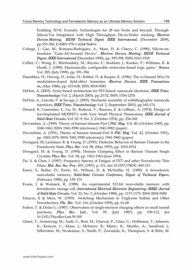
Future Memory Technology and Ferroelectric Memory as an Ultimate Memory Solution 149
Enabling 3D-IC Foundry Technologies for 28 nm Node and beyond: Through-Silicon-Via Integration with High Throughput Die-to-Wafer stacking, Electron
Devices Meeting, IEDM Technical Digest. IEEE International, (December 2009), pp.353-356, E-ISBN 978-1-4244-5640-6
Colinge, J.; Gao, M.; Romano-Rodriguez, A.; Maes, H. & Claeys, C. (1990), Silicon-on-Insulator “Gate-All-Around Device”, Electron Devices Meeting, IEDM Technical
Digest. IEEE International (December 1990), pp. 595-598, ISSN 0163-1918 Collier, C.; Wong, E.; Belohradský, M.; Raymo, F.; Stoddart, J.; Kuekes, P.; Williams, R. &
Heath, J. (1999). Electronically configurable molecular-based logic gates,” Science Vol. 285, (July 1999), pp. 391–394
Daembkes, H.; Herzog, H.; Jorke, H.; Kibbel, H. & Kasper, E. (1986). The n-channel SiGe/Si modulation-doped field-effect transistor, Electron Devices, IEEE Transactions
on, (May 1986), pp. 633-638, ISSN 0018-9383 DeHon, A. (2003). Array-based architecture for FET-based, nanoscale electronic, IEEE Trans.
Nanotechnology Vol. 2, (March 2003), pp.23-32, ISSN 1536-125X DeHon, A.; Lincoln, P. & Savage, J. (2003). Stochastic assembly of sublithographic nanoscale
interfaces, IEEE Trans. Nanotechnology Vol. 2, (September 2003), pp.165-174 Denard, R.; Gaensslen, F.; Yu, H.; Rideout, V.; Bassous, E. & LeBlanc, A. (1974). Design of
Ion-Implanted MOSFET’s with Very Small Physical Dimensions, IEEE Journal of
Solid-State Circuits, Vol. SC-9, No. 5, (October 1974), pp. 256-268 Devonshire, A. (1949). Theory of barium titanate-Part I Phil. Mag. Vol. 40, (October 1949), pp.
1040-1063, ISSN 1941-5990 (electronic); 1941-5982 (paper) Devonshire, A. (1951). Theory of barium titanate-Part II Phil. Mag. Vol. 42, (October 1951),
pp. 1065-1079, ISSN 1941-5990 (electronic); 1941-5982 (paper) Drougard, M; Landauer, R. & Young, D. (1955). Dielectric Behavior of Barium Titanate in the
Paraelectric State, Phys. Rev. Vol. 98, (May 1955), pp. 1010-1014 Drougard, M. & Young, D. (1954). Domain Clamping Effect in Barium Titanate Single
Crystals, Phys. Rev. Vol. 94, pp. 1561-1563 (June 1954) Du, X. & Chen, I. (1997). Frequency Spectra of Fatigue of PZT and other Ferroelectric Thin
Films. Mat. Res. Soc. Proc. 493, (1997), p. 311, doi 10.1557/PROC-493-311 Eaton, S.; Butler, D.; Parris, M.; Willson, D. & McNeillie, H. (1988). A ferroelectric
nonvolatile memory, Solid-State Circuits Conference, Digest of Technical Papers, (February 1988), pp. 130–131
Evans, J. & Womack, R. (1988). An experimental 512-bit nonvolatile memory with ferroelectric storage cell, International Electrical Electronic Engineering (IEEE) Journal
of Solid-State Circuits, Vol. 23, No. 5, (October 1988), pp. 1171-1175, ISSN 0018-9200 Fatuzzo, E & Merz, W. (1959). Switching Mechanism in Triglycine Sulfate and Other
Ferroelectrics, Phy. Rev. Vol. 116, (October 1959), pp. 61-68 Fulton, T. & Dolan G. (1987). Observation of single-electron charging effects in small tunnel
junctions, Phys. Rev. Lett., Vol. 59, (July 1987), pp. 109-112, doi 10.1103/PhysRevLett.59.109
Ghani, T.; Armstrong, M.; Auth, C.; Bost, M.; Charvat, P.; Glass, G.; Hoffmann, T.; Johnson, K.; Kenyon, C.; Klaus, J.; McIntyre, B.; Mistry, K.; Murthy, A.; Sandford, J.; Silberstein, M.; Sivakumar, S.; Smith, P.; Zawadzki, K.; Thompson, S. & Bohr, M.
www.intechopen.com
Ferroelectrics - Applications 150
(2003). A 90nm high volume manufacturing logic technology featuring novel 45nm gate length strained silicon CMOS transistors, Electron Devices Meeting, IEDM
Technical Digest. IEEE International, (December 2003), pp. 11.6.1-4, ISBN 0-7803-7872-5
Haun, M. Ph.D. Thesis, (1988). Thermodynamic theory of the lead zircornate-titanate solid solution
system, The Pennsylvania State University, 1988. Ch. 1 Hisamoto, D.; Kaga, T.; Kawamoto, Y. & Takeda, E. (1989). A fully depleted lean-channel
transistor (DELTA)-a novel vertical ultra thin SOI MOSFET, Electron Devices
Meeting, IEDM Technical Digest. IEEE International (December 1989), pp. 833-836 ISSN 0163-1918
Hong, Y.; Jung, D.; Kang, S.; Kim, H.; Jung, J.; Koh, H.; Park, J.; Choi, D.; Kim, S.; Ahn, W.; Kang, Y.; Kim, H.; Jung, W.; Lee, E.; Jeong, H. & Kim, K. (2007). 130 nm-technology, 0.25 um2, 1T1C FRAM Cell for SoC (System-on-a-Chip)-friendly Applications, Tech. Papers, VLSI Technology Symposium, (June 2007),pp. 230-231, ISBN978-4-900784-03-1
Hwang, C. (2006). New paradigms in the silicon industries, Electron Devices Meeting,
IEDMTechnical Digest. IEEE International, (December 2006), pp. 1-8, ISBN 1-4244-0439-8
Iijima, S. (1991). Helical microtubules of graphitic carbon, Nature, Vol. 354, (November 1991), pp. 56-58
Jaffe, B.; Cook, W. & Jaffe, H. (1971). Piezoelectric Ceramics, (Academic Press, India, 1971), p. 70 Jo, J.; Kim, D.; Kim, Y.; Choe, S.; Song, T.; Yoon, J.; & Noh, T. (2006). Polarization Switching
Dynamics Governed by the Thermodynamic Nucleation Processin Ultrathin Ferroelectric Films, Physical Review Letters, (December 2006), pp. 247602-1-4
Jona, F & Shirane, G. (1962). Ferroelectric Crystals, Pergamon Press, Oxford, Ch.1. 1962 Jung, D.; Ahn, W.; Hong, Y.; Kim, H.; Kang, Y.; Kang, J.; Lee, E.; Ko, H.; Kim, S.; Jung, W.;
Kim, J.; Kang, S.; Jung, J.; Choi, D.; Lee, S. & Jeong, H. (2008). An Endurance-free Ferroelectric Random Access Memory as a Non-volatile RAM, Tech. Papers, VLSI
Technology Symposium, (June 2008), pp. 102-103, ISBN 978-1-4244-1802-2 Jung, D.; Dawber, M.; Scott, J.; Sinammon, L. & Gregg, J. (2002). Switching dynamics in
ferroelectric thin films: an experimental survey, Integrated Ferroelectrics, Vol. 48, 2002, pp.59-68.
Jung, D.; Lee, E.; Seo, H.; Kim, J.; Park, Y.; Oh, K. & Kim, K. (2009) Data-retention time in 40 nm of technology node, 32nd. Conference of Semiconductor in Samsung, (December 2009)
Jung, D.; Lee, S.; Koo, B.; Hwang, Y.; Shin, D.; Lee, J.; Chun, Y.; Shin, S.; Lee, M.; Park, H.; Lee, S.; Kim, K. & Lee, J. (1998). A Highly Reliable 1T/1C Ferroelectric Memory, Dig. Tech. Papers, VLSI Technology Symposium, (June 1998), pp. 122-123
Jung, D.; Kim, H. & Kim, K. (2007). Key Integration Technologies for Nanoscale FRAMs, IEEE transactions on ultrasonics, ferroelectrics, and frequency control, vol. 54, no. 12, (December 2007), pp. 2535-2540 ISSN 0885-3010
Jung, S.; Jang, J.; Cho, W.; Cho, H.; Jeong, J.; Chang, Y.; Kim, J.; Rah, Y.; Son, Y.; Park, J.; Song, M.; Kim, K.; Lim, J.; Kim, K. (2006), Three Dimensionally Stacked NAND flash Memory Technology Using Stacking Single Crystal Si Layers on ILD and
www.intechopen.com

Future Memory Technology and Ferroelectric Memory as an Ultimate Memory Solution 151
TANOS Structure for Beyond 30nm Node, Electron Devices Meeting, IEDM Technical
Digest. IEEE International, (December 2006), pp. 1-4, ISBN 1-4244-0439-8 Jung, S.; Jang, J; Cho, W.; Moon, J.; Kwak, K.; Choi, B.; Hwang, B.; Lim, H.; Jeong, J.; Kim, J.
& Kim, K. (2004). The Revolutionary and Truly 3-Dimensional 25F2 SRAM Cell Technology with the smallest S3 (Stacked Single-crystal Si) Cell, 0.16um2, and SSTFT (Stacked Single-crystal Thin Film Transistor) for Ultra High Density SRAM, Tech. Papers, VLSI Technology Symposium, (June 2004), pp. 228-229, ISBN 0-7803-8289-7
Junquera, J. & Ghosez, P. (2003). Critical thickness for ferroelectricity in perovskite ultrathin
films, Nature, vol. 422, (2003), pp. 506–509 Kang, Y.; Joo, H.; Park, J.; Kang, S.; Kim, J.; Oh, S.; Kim, H.; Kang, J.; Jung, J.; Choi, D.; Lee,
E.; Lee, S.; Jeong, H. & Kim, K. (2006). World Smallest 0.34 um2 ~ COB Cell 1T1C 64Mb FRAM with New Sensing Architecture and Highly Reliable MOCVD PZT Integration Technology, Tech. Papers, VLSI Technology Symposium, (June 2006), pp. 124-125, ISBN 1-4244-0005-8
Katsumata, R.; Kito, M.; Fukuzumi, Y.; Kido, M.; Tanaka, H.; Komori, Y.; Ishiduki, M.; Matsunami, J.; Fujiwara, T.; Nagata, Y.; Zhang, L.; Iwata, Y.; Kirisawa, R.; Aochi, H. & Nitayama A. (2009). Pipe-shaped BiCS Flash Memory with 16 Stacked Layers and Multi-Level-Cell Operation for Ultra High Density Storage Devices, Dig. Tech.
Papers, VLSI Technology Symposium, (June 2009), pp. 136 – 137, ISBN 978-1-4244-3308-7
Kawamura, S.; Sasaki, N.; Iwai, T.; Nakano, M. & Takagi, M. (1983). Three-Dimensional CMOS ICS Fabricated by Using Beam Crystallization, Electron Device Letters, IEEE,
Vol. 4, (Octorber 1983), pp. 366-368, ISSN 0741-3106 Key, H. & Dunn, J. (1962). Thickness dependence of the nucleation field of triglycine
sulphate, (December 1962). Phil. Mag. 7, pp. 2027-2034, ISSN 1478-6443 Keeny, S. (2001). A 130nm Generation High Density Etox Flash Memory Technology,
Electron Devices Meeting, IEDM Technical Digest. IEEE International, (December 2001), pp. 2.5.1-4, ISBN 0-7803-7050-3
Kim, D.; Jo, J.; Kim, Y.; Chang, Y.; Lee, J.; Yoon, J.; Song, T.; &. Noh, T. (2005). Polarization Relaxation Induced by a Depolarization Field in Ultrathin Ferroelectric BaTiO3 Capacitors, Physical Review Letters, (December 2005), pp. 237602-1-4
Kim, D.; Kim, J.; Huh, M.; Hwang, Y.; Park, J.; Han, D.; Kim, D.; Cho, M.; Lee, B.; Hwang, H.; Song, J.; Kang, N.; Ha, G.; Song, S.; Shim, M.; Kim, S.; Kwon, J.; Park, B.; Oh, H.; Kim, H.; Woo, D.; Jeong, M.; Kim, Y.; Lee, Y.; Shin, J.; Seo, J.; Jeong, S.; Yoon, K.; Ahn, T.; Lee, J.; Hyung, Y.; Park, S.; Choi, W.; Jin, G.; Park, Y. & Kim, K. (2004a). A mechanically enhanced storage node for virtually unlimited height (MESH) capacitor aiming at sub 70nm DRAMs, Electron Devices Meeting, IEDM Technical
Digest. IEEE International, (December 2004), pp. 69-72, ISBN: 0-7803-8684-1 Kim, H.; Song, Y.; Lee, S.; Joo, H.; Jang, N.; Jung, D.; Park, Y.; Park, S.; Lee, K.; Joo, S.; Lee, S.;
Nam, S. & Kim, K. (2002). Novel integration technologies for highly manufacturable 32Mb FRAM, Dig. Tech. Papers, VLSI Technology Symposium, (June 2002), pp.210-211
www.intechopen.com
Ferroelectrics - Applications 152
Kim, J.; Lee, C.; Kim, S.; Chung, I.; Choi, Y.; Park, B.; Lee, J.; Kim, D.; Hwang, Y.; Hwang, D.; Hwang, H.; Park, J.; Kim, D.; Kang, N.; Cho, M.; Jeong, M.; Kim, H.; Han, J.; Kim, S.; Nam, B.; Park, H.; Chung, S.; Lee, J.; Park, J.; Kim, H.; Park, Y. & Kim, K. (2003). The breakthrough in data retention time of DRAM Using Recess-Channel-Array Transistor (RCAT) for 88nm feature size and beyond”, Dig. Tech. Papers,VLSI
Technology Symposium, (June 2003), pp. 11-12, ISBN 4-89114-033-X Kim, K. (2010). From the future silicon technology perspective: Opportunities and
challenges, Electron Devices Meeting, IEDM Technical Digest. IEEE International, (December 2010), pp. 1-9
Kim, K. & Choi, J. (2006). Future outlook of NAND flash technology for 40 nm node and beyond, Proceedings of the IEEE Non-Volatile Semiconductor Memory Workshop, (2006) pp. 9-11
Kim, K. & Jeong, G. (2005). Memory technologies in Nano-era: Challenges and Opportunities, Solid-State Circuits Conference, 2005. Digest of Technical Papers. ISSCC.
2005 IEEE International, (February 2005), pp. 576-577, ISSN 0193-6530 Kim, K.; Hwang, C. & Lee, J. (1998). DRAM Technology perspective for Giga-bit era, IEEE
Transaction of Electronic Devices, Vol.45, (March 1998), pp.598-608, ISSN 0018-9383 Kim, S.; Xue, L. & Tiwari, S. (2004b). Low Temperature Silicon Layering for Three-
Dimensional Integration, SOI Conference, 2004. Proceedings. 2004 IEEE International, (October 2004), pp. 136-138, ISBN 0-7803-8497-0
Kinney, W.; Shepherd, W.; Miller, W.; Evans J. & Womack, R. (1987). A nonvolatile memory cell based ferroelectric storage capacitors, Electron Devices Meeting, IEDM Technical
Digest. IEEE International, (December 1987), pp. 850-853 Kryder, M. & Kim, C. (2009). After Hard Drives—What Comes Next?, IEEE transactions on,
magnetics, Vol. 45, No. 10, (October 2009), pp. 3406-3413 Landauer, R. (1957). Electrostatic Considerations in BaTiO3 Domain Formation during
Polarization Reversal, Journal of Applied Physics, (February 1957), Vol. 28, pp. 227-234
Landauer, R; Young, D. & Drougard, M. (1956). Polarization Reversal in the Barium Titanate Hysteresis Loop, J. Appl. Phys. Vol. 27, (July 1956), pp. 752-758
Lee, C.; Hur, S.; Shin, Y.; Choi, J.; Park, D. & Kim, K. (2005). Charge-trapping device structure of SiO2/SiN/high-k dielectric Al2O3 for high-density flash memory, Appl.
Phys. Lett. Vol. 86, (April 2005), pp. 152908-1-152908-3 Lee, C.; Yoon, J.; Lee, C.; Yang, H.; Kim, K.; Kim, T.; Kang, H.; Ahn, Y.; Park, D. & Kim, K.
(2004). Novel Body Tied FinFET Cell Array Transistor DRAM with Negative Word Line Operation for Sub 60nm Technology and Beyond”, Dig. Tech. Papers, VLSI
Technology Symposium, (June 2004), p.130, ISBN: 0-7803-8289-7 Lee, J.; Ahn, Y.; Park, Y.; Kim, M.; Lee, D.; Lee, K.; Cho, C.; Chung, T. & Kim, K. (2003a).
Robust memory cell capacitor using multi-stack storage node for high performance in 90 nm technology and beyond, Dig. Tech. Papers, VLSI Technology Symposium, June 2003), pp. 57 – 58, ISBN 4-89114-033-X
Lee, J.; Lee, J.; Lee, J.; Jeong, T. & Kim, K. (2008). GiDL engineering in 50 nm of technology node, 31st. Conference of Semiconductor in Samsung, (December 2008)
www.intechopen.com
Future Memory Technology and Ferroelectric Memory as an Ultimate Memory Solution 153
Lee, S.; Lee, J.; Choe, J.; Cho, E.; Ahn, Y.; Hwang, W.; Kim, T.; Kim, W.; Yoon, Y.; Jang, D.; Yoo, J.; Kim, D.; Park, K.; Park, D. & Ryu, B. (2006). Improved post-cycling characteristic of FinFET NAND flash, Electron Devices Meeting, IEDM Technical
Digest. IEEE International, (December 2006), pp. 1-4, ISBN 1-4244-0438-X Lee, S.; Jung, D.; Song, Y.; Koo, B.; Park, S.; Cho, H.; Oh, S.; Hwang, D.; Lee, S.; Lee, J.; Park,
Y.; Jung, I. & Kim, K. (1999). A FRAM Technology using 1T1C Triple Metal layers for High Performance and High Density FRAMs, Tech. Papers, VLSI Technology
Symposium, (June 1999), p. 141-142 Lee, S.; Kim, S.; Yoon, E.; Oh, C.; Chung, I.; Park, D. & Kim, K. (2003b). A novel multibridge-
channel MOSFET (MBCFET): fabrication technologies and characteristics, Nanotechnology, IEEE Transactions on (December 2003), pp. 253-256, ISSN 1536-125X
Li, J.; Eastman, A.; Li, Z.; Foster, C.; Newnham, R. & Cross, L. (1996). Size effects in
nanostructured ferroelectrics, Phys. Lett. A, vol. 212, pp. 341–346, 1996 Lines, M & Glass, A. (1979). Principles and applications of ferroelectrics and related materials,
Clarendon Press, Oxford, 1979 Merz, W. (1953). Double Hysteresis Loop of BaTiO3 at the Curie Point, Phys. Rev., Vol. 91,
(August 1953), pp. 513-517 Merz, W. (1954). Domain Formation and Domain Wall Motions in Ferroelectric BaTiO3
Single Crystals, Phys. Rev. Vol. 95, (August 1954), pp. 690–698 Moazzami, R.; Maniar, P.; Jones, R.; Campbell, A. & Mogab, C. (1992). Ultra-high charge
storage capacity ferroelectric lead zirconate titanate thin films for gigabit-scale DRAMs, Electron Devices Meeting, IEDM Technical Digest. IEEE International, (December 1992), pp. 973-976
Moore, G. (1965). Cramming more components onto integrated circuits, Electronics Magazine, 19 (April 1965). pp. 24-27
Moore, G. (2006). Moore’s Law at Forty, Understanding Moore’s Law, D.C. Brock, ed., Chemical
Heritage Foundation, p. 76 Mori, S.; Sakagami, E.; Araki, H.; Kaneko, Y.; Narita, K.; Ohshima, Y.; Arai, N. & Yoshikawa,
K. (1991). ONO inter-poly dielectric scaling for nonvolatile memory applications, IEEE Transactions on Electron Devices, Vol. 38, No. 2, (August 1991) pp. 386-391, ISSN 0018-9383
Morrison, F.; Jung, D. & Scott, J. (2005). In collaboration with Saad et al., 2004a, we independently evaluate the dielectric behaviors as a function of temperature in BaTiO3 single crystal with a range from 447 to 77 nm.
Nagarajan, V; Prasertchoung, S.; Zhao, T.; Zheng, H.; Ouyang, J.; Ramesh, R.; Tian, W.; Pan, X.; Kim, D. & Eom, C. (2004). Size effects in ultrathin epitaxial ferroelectric
heterostructures, Appl. Phys. Lett., vol. 84, no. 25, (June 2004), pp. 5225–5227, doi:10.1063/1.1765742
Nakajima, A.; Futatsugi, T.; Nakao, H.; Usuki, T.; Horiguchi, N. & Yokoyama, N. (1998). Microstructures and electrical properties of Sn nanocrystals in thin thermally grown SiO2 formed via low energy implantation, Journal of Applied Physics, vol. 84, no 3, (August 1998), pp.1316-1320
www.intechopen.com

Ferroelectrics - Applications 154
Neudeck, G.; Su, T. & Denton, J. (2000). Novel Silicon Epitaxy for Advance MOSFET Devices, Electron Devices Meeting, IEDM Technical Digest. IEEE International, (December 2000), pp. 169-173, ISBN 0-7803-6438-4
Ohno, Y.; Horikawa, T.; Shinkawata, H.; Kashihara, K.; Kuroiwa, T.; Okudaira, T.; Hashizume, Y.; Fukumoto, K.; Eimori, T.; Shibano, T.; Arimoto, K.; Itoh, H.; Nishimura, T. & Miyoshi, H. (1994). A memory cell capacitor with BaxSr1-xTiO3 (BST) film for advanced DRAMs, Dig. Tech. Papers, VLSI Technology Symposium, (June 1994), pp. 149 – 150, ISBN 0-7803-1921-4
Park, J.; Hur, H.; Lee, J.; Park, J.; Sel, J.; Kim, J.; Song, S.; Lee, J.; Lee, J.; Son, S.; Kim, Y.; Park, M.; Chai, S.; Choi, J.; Chung, U.; Moon, J.; Kim, K.; Kim, K. & Byung-Il Ryu, B. (2004). 8Gb MLC (Multi-Level Cell) NAND flash Memory using 63nm Process Technology, Electron Devices Meeting, IEDM Technical Digest. IEEE International, (December 2004), pp. 873-876, ISBN: 0-7803-8684-1
Park, Y.; Choi, J.; Kang, C.; Lee, C.; Shin, Y.; Choi, B.; Kim, J.; Jeon, S.; Sel, J.; Park, J.; Choi, K.; Yoo, T.; Sim, J. & Kim, K. (2006). Highly manufacturable 32 Gb multi-level NAND flash memory with 0.0098 nm2 cell size using TANOS (Si-oxide-nitride-Al2O3-TaN), Electron Devices Meeting, IEDM Technical Digest. IEEE International, (December 2006), pp. 1-4, ISBN 1-4244-0438-X
Parker, C.; Maria, J. & Kingon, A. (2002) Temperature and thickness dependent permittivity of BaSrTiO3 thin films, Appl. Phys. Lett. Vol.81, (July 2002), pp. 340-342
Pulvari, C. & Kuebler, W. (1958). Polarization Reversal in Tri‐Glycine Fluoberyllate and Tri‐Glycine Sulfate Single Crystals, J. Appl. Phys. Vol. 29, (December 1958), pp. 1742-1746
Rao, V.; Ho, S.; Vincent, L.; Li, H.; Liao, E.; Nagarajan, R.; Chai, T.; Xiaowu, Z. & Damaruganath, P. (2009). TSV Interposer Fabrication for 3D IC Packaging, Electronics Packaging Technology Conference, 2009. EPTC '09. 11th, (December 2009), p. 431, (2009), ISBN 978-1-4244-5100-5
Remeika, J. & Morrison Jackson, W. (1954). A Method for Growing Barium Titanate Single Crystals, J. Am. Chem. Soc., 76 (3), (February 1954), pp. 940–941 DOI 10.1021/ja01632a107
Saad, M.; Baxter, P.; Bowman, R.; Gregg, J.; Morrison, F. & Scott, J. (2004a). Intrinsic dielectric response in ferroelectric nano-capacitors J. Phys.: Condens. Matter Vol. 16, (October 2004), pp. L451–L456
Saad, M.; Baxer, P.; McAneney, J.; Lookman, A.; Sinnamon, L.; Evans, P.; Schilling, A.; Adams, T.; Zhu, X.; Pollard, R.; Bowman, R.; Gregg, J.; Jung, D.; Morrison, F. & Scott, J. (2006). Investigating the effects of reduced size on the properties of ferroelectrics, IEEE Transactions on Ultrasonics Ferroelectrics and Frequency Control, Vol. 53, (December 2006) pp.2208-2225
Saad, M.; Bowman, R. & Gregg, J. (2004b). Characteristics of single crystal thin film capacitor structures made using a focused ion beam microscope, Appl. Phys. Lett. Vol. 84, (February 2004), pp. 1159-1161
Shaw, T.; Suo, Z.; Huang, M.; Liniger, E.; Laibowitz, R. & Baniecki, J. (1999). The effect of stress on the dielectric properties of barium strontium titanate thin films, Appl.
Phys. Lett. Vol. 75, (October 1999), pp. 2129-2131
www.intechopen.com

Future Memory Technology and Ferroelectric Memory as an Ultimate Memory Solution 155
Shiga, H.; Takashima, D.; Shiratake, S.; Hoya, K.; Miyakawa, T.; Ogiwara, R.; Fukuda, R.; Takizawa, R.; Hatsuda, K.; Matsuoka, F.; Nagadomi, Y.; Hashimoto, D.; Nishimura, H.; Hioka, T.; Doumae, S.; Shimizu, S.; Kawano, M.; Taguchi, T.; Watanabe, Y.; Fujii,S.; Ozaki,T.; Kanaya,H.;Kumura,Y.; Shimojo,Y.; Yamada,Y.; Minami,Y.; Shuto, S.; Yamakawa, K.; Yamazaki, S.; Kunishima, I.; Hamamoto, T.; Nitayama, A. & Furuyama, T. (2009). A1.6 GB/s DDR2 128 Mb chain FeRAM with scalable octal bitline and sensing schemes, Solid-State Circuits Conference, Digest of Technical
Papers, Session 27, (Feb. 2009), pp. 464–465, ISBN 978-1-4244-3458-9 Shin, Y.; Choi, J.; Kang, C.; Lee, C.; Park, K.; Lee, J.; Sel, J.; Kim, V.; Choi, B.; Sim, J.; Kim, D.;
Cho, H. & Kim K. (2006) A Novel NAND-type MONOS Memory using 63nm Process Technology for Multi-Gigabit Flash EEPROMs, Electron Devices Meeting, IEDM Technical Digest. IEEE International, (December 2006), pp. 327-330, ISBN 0-7803-9268-x
Sirringhaus, H.; Tessler, N. & Friend, R. (1998). Integrated Optoelectronic Devices Based on Conjugated Polymers, Science Vol. 280, (June 1998), pp. 1741-1744
Song, Y.; Kim, H.; Lee, S.; Jung, D.; Koo, B.; Lee, J.; Park, Y.; Cho, H.; Park, S. & Kim, K. (1999). Integration and Electrical Properties of Diffusion Barrier for High Density Ferroelectric Memory, Applied Physics Letters, Vol. 76, (November 1999), pp. 451-453
Streiffer, S.; Eastman, J.; Fong, D.; Thompson, C.; Munkholm, A.; Ramana Murty, M.; Auciello, O; Bai, G. & Stephenson, G. (2002). Observation of nanoscale 180 degrees stripe domains in ferroelectric PbTiO3 thin films, Phys. Rev. Lett., vol. 89, (2002), no. 067601
Sumi, T.; Azuma, M.; Otsuki, T.; Gregory, J. & Araujo, C. (1995). A 0.9 V embedded ferroelectric memory for microcontrollers, Solid-State Circuits Conference, Digest of
Technical Papers, (February 1995), pp. 70-71, ISBN 0-7803-2495-1 Supriyo Datta & Biswajit Das (1990). Electronic analog of the electro-optic modulator, Appl.
Phys. Lett., Vol. 56, (February 1990), pp.665-667, doi:10.1063/1.102730 Tanabe, N.; Matsuki, T.; Saitoh, S.; Takeuchi, T.; Kobayashi, S.; Nakajima, T.; Maejima, Y. ;
Hayashi, Y.; Amanuma, K.; Hase, T.; Miyasaka, Y. & Kunio, T. (1995). A ferroelectric capacitor over bit-line (F-COB) cell for high density nonvolatile ferroelectric memories, Dig. Tech. Papers, VLSI Technology Symposium, (June 1995), pp. 123 –124, ISBN 0-7803-2602-4
Tiwari, S.; Rana, F.; Chan, K.; Hanafi, H.; Wei C. & Buchanan, D. (1995). Volatile and nonvolatile memories in silicon with nano crystal storage, Electron Devices Meeting, IEDM Technical Digest. IEEE International, (December 1995), pp.521-524, ISBN 0-7803-2700-4
Topol, A.; Tulipe, D.; La Shi, L.; Frank, D.; Bernstein, K.; Steen, S.; Kumar, A.; Singco, G.; Young, A.; Guarini, K.; Jeong, M. (2006). Three-dimensional integrated circuits, IBM Journal of Research and Development, (July 2006), pp. 491–506, ISSN 0018-8646
Triebwasser, S. (1956). Behavior of Ferroelectric KNbO3 in the Vicinity of the Cubic-Tetragonal Transition, Phys. Rev., Vol. 101, (February 1956), pp. 993-997
Tybell, T.; Ahn, C. & Triscone, J. (1999). Ferroelectricity in thin perovskite films, Appl. Phys.
Lett., vol. 75, no. 6, pp. 856–858, 1999.
www.intechopen.com
Ferroelectrics - Applications 156
Valasek, J. (1921). Piezo-electric and allied phenomena in Rochelle Salt, Phys. Rev. Vol. 17, (April 1921), pp. 475-481
Wada, Y. (2002). Prospects for Single-Molecule Information-Processing Devices for the Next Paradigm, Ann. New York Acad. Sci. 960, (April 2002), pp. 39-61
Whang, D.; Jin, S.; Wu, Y. & Lieber, C. (2003). Large-Scale Hierarchical Organization of Nanowire Arrays for Integrated Nanosystems, Nano Letters, Vol. 3, No. 9, (July 2003), pp. 1255-1259
Wieder, H. (1958). Ferroelectric Polarization Reversal in Rochelle Salt, Phys. Rev. Vol. 110, (April 1958), pp. 29-36
Wilk, G.; Wallace, R. & Anthony, J. (2001). High-κ dielectrics: Current status and materials properties considerations, Journal of Applied physics, Vol. 89, No. 10, (January 2001), pp. 5243-5275.
Yanson, A.; Rubio Bollinger, G.; Van den Brom, H.; Agraı¨t, N. & Van Ruitenbeek, J. (1998). Formation and manipulation of a metallic wire of single gold atoms, Nature, Vol. 395, (October 1998), pp. 783-785
Yim, Y.; Shin, K.; Hur, S.; Lee, J.; Balk, I; Kim, H.; Chai, S.; Choi, E.; Park, M.; Eun, D.; Lee, S.; Lim, H.; Youn, S.; Lee, S.; Kim, T.; Kim, H.; Park, K & Kim, K. (2003). 70nm NAND flash technology with 0.025 μm2 cell size for 4Gb flash memory, Electron Devices
Meeting, IEDM Technical Digest. IEEE International, (December 1995), pp. 34.1.1-4 ISBN 0-7803-7872-5
Yoon, J.; Lee, K.; Park, S.; Kim, S.; Seo, H.; Son, Y.; Kim, B.; Chung, H.; Lee, C.; Lee, W.; Kim, D.; Park, D.; Lee, W. & Ryu, B. (2006). A Novel Low leakage Current VPT (Vertical Pillar Transistor) Integration for 4F2 DRAM Cell Array with sub 40 nm Technology, 64th Device Reearch Conference (DRC) Digest, (June 2006), pp.259-260, ISSN 1548-3770
Zhong, Z.; Wang, D.; Cui, Y.; Bockrath, M. & Lieber, C. (2003). Nanowire Crossbar Arrays as Address Decoders for Integrated Nanosystems," Science Vol. 302, (November 2003), pp.1377- 1379
www.intechopen.com
Ferroelectrics - ApplicationsEdited by Dr. Mickaël Lallart
ISBN 978-953-307-456-6Hard cover, 250 pagesPublisher InTechPublished online 23, August, 2011Published in print edition August, 2011
InTech EuropeUniversity Campus STeP Ri Slavka Krautzeka 83/A 51000 Rijeka, Croatia Phone: +385 (51) 770 447 Fax: +385 (51) 686 166www.intechopen.com
InTech ChinaUnit 405, Office Block, Hotel Equatorial Shanghai No.65, Yan An Road (West), Shanghai, 200040, China Phone: +86-21-62489820 Fax: +86-21-62489821
Ferroelectric materials have been and still are widely used in many applications, that have moved from sonartowards breakthrough technologies such as memories or optical devices. This book is a part of a four volumecollection (covering material aspects, physical effects, characterization and modeling, and applications) andfocuses on the application of ferroelectric devices to innovative systems. In particular, the use of thesematerials as varying capacitors, gyroscope, acoustics sensors and actuators, microgenerators and memorydevices will be exposed, providing an up-to-date review of recent scientific findings and recent advances in thefield of ferroelectric devices.
How to referenceIn order to correctly reference this scholarly work, feel free to copy and paste the following:
Kinam Kim and Dong Jin Jung (2011). Future Memory Technology and Ferroelectric Memory as an UltimateMemory Solution, Ferroelectrics - Applications, Dr. Mickaël Lallart (Ed.), ISBN: 978-953-307-456-6, InTech,Available from: http://www.intechopen.com/books/ferroelectrics-applications/future-memory-technology-and-ferroelectric-memory-as-an-ultimate-memory-solution

© 2011 The Author(s). Licensee IntechOpen. This chapter is distributedunder the terms of the Creative Commons Attribution-NonCommercial-ShareAlike-3.0 License, which permits use, distribution and reproduction fornon-commercial purposes, provided the original is properly cited andderivative works building on this content are distributed under the samelicense.