galaxy d32 epfl 001 6 final gals design flow tutorial€¦ · ·...
TRANSCRIPT
GALAXY GALS InterfAce for CompleX Digital
SYstem Integration
Confid. Level:
Date :
Issue:
Public
01/12/2010
1
GALAXY_D32_EPFL_001_6_Final_GALS_Design_Flow_Tutorial.doc PAGE: 1/40
Deliverable – D32
Final GALS Design Flow Tutorial
Grant Agreement No: 214364
Project acronym: GALAXY
Project title: GALS InterfAce for CompleX Digital System Integration
Funding Scheme: STREP
Date of latest version of Annex I against
which the assessment will be made: 22.03.2010.
Contractual Date of Delivery to the EC: 30 Nov 2010
Actual Date of Delivery to the EC: 1 Dec 2010
Author(s): Lilian Janin (UNIMAN), Milos Krstic, Xin Fan (IHP), Milos Stanisavljevic (EPFL), Christoph Heer (Infineon)
Participant(s): UNIMAN, IHP, EPFL, INFINEON
Work Package: WP5
Security: Public
Nature: Report
Version: 1
Total number of pages: 40
Abstract:
This tutorial explains the main steps in GALS design flow, including the new tools targeted for GALS systems design. It shows how software GALAXY GALS design tools are used during GALAXY project to reach the final chip. All design phases included design specification, simulation, synthesis, post-synthesis simulation, back-end and post-layout simulation are covered. GALS test flow is also presented. Strategy for co-synthesis of asynchronous and synchronous components, and for successful constraining of the GALS design and possible optimization and automation of synthesis flow for GALS designs is presented. Moreover, GALS system layout using hierarchical and flat approach is illustrated. Insertion of asynchronous components is performed as hard macros and as a set of standard cell components.
Keyword list: asynchronous, back-end, design flow, GALS, layout, macros, place and route, tutorial, synthesis

GALAXY GALS InterfAce for CompleX Digital
SYstem Integration
Confid. Level:
Date :
Issue:
Public
01/12/2010
1
GALAXY_D32_EPFL_001_6_Final_GALS_Design_Flow_Tutorial.doc PAGE: 2/40
Function Responsibility Date Signature
Written by:
Lilian Janin, Milos Krstic, Milos Stanisavljevic, Christoph Heer
5 Oct 2010
Checked by:
Members of GALAXY Consortium
Approved by:
-
Reserved to EC
Approved by:

GALAXY GALS InterfAce for CompleX Digital
SYstem Integration
Confid. Level:
Date :
Issue:
Public
01/12/2010
1
GALAXY_D32_EPFL_001_6_Final_GALS_Design_Flow_Tutorial.doc PAGE: 3/40
CHANGE RECORDS
ISSUE DATE § : CHANGE RECORD AUTHOR
1 5-Oct-10 1st version Lilian Janin
2 11-Nov-10 Document reformatted and IHP content added Milos Krstic
3 18-Nov-10 EPFL content added Milos Stanisavljevic
4 24-Nov-10 UNIMAN content updated Lilian Janin
5 26-Nov-10 Final updates by EPFL Milos Stanisavljevic
6 1-Doc-10 Final check & Industry view Milos Krstic, Christoph Heer

GALAXY GALS InterfAce for CompleX Digital
SYstem Integration
Confid. Level:
Date :
Issue:
Public
01/12/2010
1
GALAXY_D32_EPFL_001_6_Final_GALS_Design_Flow_Tutorial.doc PAGE: 4/40
BIBLIOGRAPHIC RECORD
Project Number: 214364 GALAXY
Project Title: GALAXY
Deliverable Type: Report
Deliverable Number: D32
Contractual Date of Delivery: 30 Nov 2010
Actual Date of Delivery: 1 Dec 2010
Title of Deliverable: Final GALS Design Flow Tutorial
Work package contributing to the Deliverable:
WP5
Authors: Lilian Janin, Milos Krstic, Milos Stanisavljevic, Christoph Heer
Abstract This tutorial explains the main steps in GALS design flow, including the new tools targeted for GALS systems design. It shows how software GALAXY GALS design tools are used during GALAXY project to reach the final chip. All design phases included design specification, simulation, synthesis, post-synthesis simulation, back-end and post-layout simulation are covered. GALS test flow is also presented. Strategy for co-synthesis of asynchronous and synchronous components, and for successful constraining of the GALS design and possible optimization and automation of synthesis flow for GALS designs is presented. Moreover, GALS system layout using hierarchical and flat approach is illustrated. Insertion of asynchronous components is performed as hard macros and as a set of standard cell components.
Keywords asynchronous, back-end, design flow, GALS, layout, macros, place and route, tutorial, synthesis
Confidentiality Level Public
Name of Client: EC
Distribution List: GALAXY, EC, internet
Authorised by:
Issue: 1
Document ID: D32
Total Number of Pages: 40
Contact Details: [email protected]

GALAXY GALS InterfAce for CompleX Digital
SYstem Integration
Confid. Level:
Date :
Issue:
Public
01/12/2010
1
GALAXY_D32_EPFL_001_6_Final_GALS_Design_Flow_Tutorial.doc PAGE: 5/40
TABLE OF CONTENTS
1 INTRODUCTION ............................................................................................................7
2 REFERENCES ...............................................................................................................8
2.1 ACRONYMS .............................................................................................................8
2.2 REFERENCE DOCUMENTS ....................................................................................8
3 GALAXY GALS DESIGN FLOW ....................................................................................9
4 FIRST STEPS - SPECIFICATION AND BEHAVIORAL CODING ................................ 10
4.1 DESIGN SPECIFICATION...................................................................................... 10
4.2 BEHAVIOURAL LEVEL CODING .......................................................................... 12
5 GALAXY DESIGN TOOLS UNDER GPL ..................................................................... 15
5.1 ASYNCHRONOUS-SYNCHRONOUS CO-SIMULATION....................................... 15
5.2 PROJECT IMPORT IN GALAXY TOOLS ............................................................... 15
5.2.1 VHDL2ASIP .....................................................................................................15
5.2.2 AsipIDE............................................................................................................15
5.3 SIMULATION.......................................................................................................... 18
5.4 CO-SIMULATIONS................................................................................................. 20
5.4.1 VHDL-STG co-simulation ...............................................................................20
5.5 SUMMARY ............................................................................................................. 22
6 AUTOMATION OF SYNTHESIS FLOW FOR GALS .................................................... 23
6.1 SYNTHESIS............................................................................................................ 23
6.1.1 Timing Constraints in Moonrake Chip Design..............................................25
6.2 POST-SYNTHESIS SIMULATION .......................................................................... 31
7 STRATEGIES FOR LAYOUT OF GALS CIRCUITS..................................................... 32
7.1 BACK-END LAYOUT ............................................................................................. 32
7.2 POST-LAYOUT SIMULATION................................................................................ 33
7.3 SIGN-OFF AND TAPE-OUT ................................................................................... 34
8 GALS TEST FLOW ...................................................................................................... 35
9 GALS DESIGN TUTORIAL EVALUATION FROM INDUSTRIAL PERSPECTIVE ....... 39
10 CONCLUSIONS ........................................................................................................... 40

GALAXY GALS InterfAce for CompleX Digital
SYstem Integration
Confid. Level:
Date :
Issue:
Public
01/12/2010
1
GALAXY_D32_EPFL_001_6_Final_GALS_Design_Flow_Tutorial.doc PAGE: 6/40
LIST OF FIGURES
Figure 1: GALS Design flow............................................................................................. 9
Figure 2: Architecture of Moonrake chip ...................................................................... 10
Figure 3: OFDM transmitter dataflow ............................................................................ 11
Figure 4: Topology of GALS OFDM transmitter............................................................ 13
Figure 5: STG of asynchronous I/O port controllers .................................................... 14
Figure 6: Initial view of the baseband processor in AsipIDE....................................... 16
Figure 7: Reorganised view of the baseband processor in AsipIDE........................... 17
Figure 8: AsipIDE navigation capabilities ..................................................................... 17
Figure 9: Focus on FFT module..................................................................................... 18
Figure 10: Modelsim simulation views............................................................................ 19
Figure 11: Simulation events mapped on Graph View connections ............................. 20
Figure 12: Original STG of GALS components DO and PI ............................................. 21
Figure 13: STG in ASIP and co-simulation STG-VHDL................................................... 21
Figure 14: Clock dependency in GALS OFDM transmitter............................................. 24
Figure 15: Synthesized netlist of I/O port controllers using Petrify .............................. 25
Figure 16: The structure of pausible clock generator .................................................... 25
Figure 17: Port allocation of I/O port controllers............................................................ 26
Figure 18: Data transfer across GALS blocks ................................................................ 27
Figure 19: Communication scheme between GALS design and outside...................... 29
Figure 20: Preferred placement of hard macros in GALS design.................................. 30
Figure 21: Final layout of Moonrake chip........................................................................ 33
Figure 22: Simplified Test Flow ....................................................................................... 37
LIST OF TABLES
Table 1: Power Estimation and System partitioning of GALS OFDM Transmitter ....... 12

GALAXY GALS InterfAce for CompleX Digital
SYstem Integration
Confid. Level:
Date :
Issue:
Public
01/12/2010
1
GALAXY_D32_EPFL_001_6_Final_GALS_Design_Flow_Tutorial.doc PAGE: 7/40
1 INTRODUCTION
This report describes the final deliverable of the GALAXY project: a GALS design flow tutorial based on the outcomes of all the research tasks, and describing how to use the tools developed as part of the project to create GALS circuits.
This tutorial starts by explaining how to use the software GALAXY GALS design tools following the route taken during the GALAXY project to design the final chip. All the main phases of design flow are covered with this tutorial – design specification, import of synchronous design and GALSification with co-simulation, synthesis and back-end.
An existing fully synchronous version of the baseband processor is first GALSified. We show how the GALAXY design tools can be used to import the synchronous baseband processor project and process it iteratively, using various co-simulations to validate the new design at each iteration.
We then describe how to tailor the synthesis flow to one’s own cell libraries. Based on design experience from WP8 (which culminated with the fabrication of the GALS baseband processor chip in 45nm), we documented the most effective approaches for synthesis and layout of a GALS chip. This includes a strategy for co-synthesis of asynchronous and synchronous components, and for successful constraining of the GALS design and possible optimization and automation of synthesis flow for GALS designs.
GALS system layout strategies are presented and illustrated using hierarchical and flat approach. An overview of existing approaches from literature survey is provided for comparison purposes in order to demonstrate the cutting-edge level of our approach. We explain the insertion of asynchronous components as hard macros and as a set of standard cell components. Obtaining timing closure in GALS layout is also discussed.
This document has also been evaluated from an industrial perspective.
In this document, due to the significant topic overlap, we have used when necessary the text parts from deliverable D33 (System Integration with GALS) and D16 (GALS test flow).

GALAXY GALS InterfAce for CompleX Digital
SYstem Integration
Confid. Level:
Date :
Issue:
Public
01/12/2010
1
GALAXY_D32_EPFL_001_6_Final_GALS_Design_Flow_Tutorial.doc PAGE: 8/40
2 REFERENCES
2.1 ACRONYMS
ASIP Asynchronous-Synchronous IPs packaging format
CAD Computer Aided Design
DRC Design Rule Check
ELF Executable and Linkable Format
EMI Electromagnetic interference
FFT Fast Fourier Transform
FIFO First In First Out
FPGA Field-Programmable Gate Array
GALS Globally Asynchronous Locally Synchronous
IP Intellectual Property
LVS Layout Versus Schematic
OFDM Orthogonal Frequency-Division Multiplexing
QDI Quasi-Delay-Insensitive
RTL Register-Transfer-Level
STG Signal Transition Graph
VHDL VHSIC Hardware Description Language
VHSIC Very-High-Speed Integrated Circuits
XML eXtendible Markup Language
2.2 REFERENCE DOCUMENTS
Ref. Document Title
[FAN09] X. Fan, M. Krstić, E. Grass, Analysis and Optimization of Pausible Clocking based GALS Design, In Proc. of XXVII IEEE International Conference on Computer Design (ICCD) 2009, Resort at Squaw Creek, Lake Tahoe, California, pp. 358-365, "Best Paper" award
[NAJ07] M. Najibi, K. Saleh, and H. Pedram, Using standard ASIC back-end for QDI asynchronous circuits: dealing with isochronic fork constraint. In Proceedings of the 17th ACM Great Lakes symposium on VLSI (GLSVLSI) 2007, pp. 299-304.
[SF01] J. Sparsø, S. Furber, R. van Leuken, R. Nouta, and A. de Graaf, Principles of Asynchronous Circuit Design: A Systems Perspective. Kluwer Academic Publishers, Boston, 2001.
[SOT02] C. P. Sotiriou, Implementing asynchronous circuits using a conventional EDA tool-flow. In Proceedings of the 39th annual Design Automation Conference (DAC) 2002, pp. 415-418.
GALAXY GALS InterfAce for CompleX Digital
SYstem Integration
Confid. Level:
Date :
Issue:
Public
01/12/2010
1
GALAXY_D32_EPFL_001_6_Final_GALS_Design_Flow_Tutorial.doc PAGE: 9/40
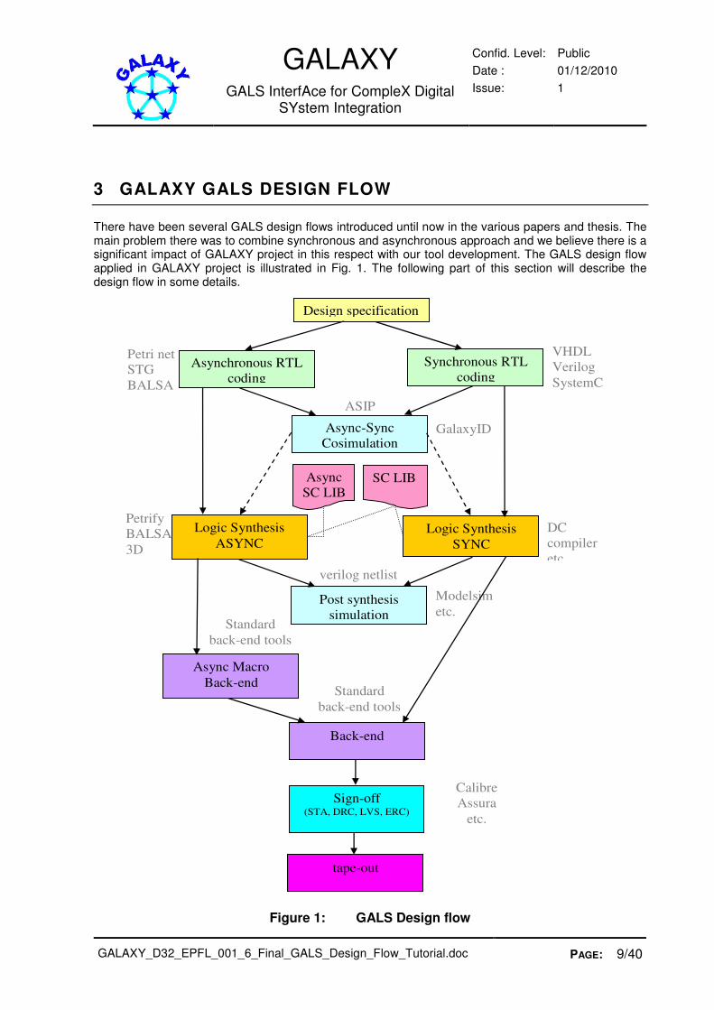
3 GALAXY GALS DESIGN FLOW
There have been several GALS design flows introduced until now in the various papers and thesis. The main problem there was to combine synchronous and asynchronous approach and we believe there is a significant impact of GALAXY project in this respect with our tool development. The GALS design flow applied in GALAXY project is illustrated in Fig. 1. The following part of this section will describe the design flow in some details.
Design specification
Asynchronous RTL
coding
Synchronous RTL
coding
Petri net
STG
BALSA
VHDL
Verilog
SystemC
Async-Sync
Cosimulation GalaxyID
E
ASIP
Logic Synthesis
ASYNC Logic Synthesis
SYNC
Async
SC LIB SC LIB
Petrify
BALSA
3D
DC
compiler
etc.
Post synthesis
simulation
Modelsim
etc.
verilog netlist
Async Macro
Back-end
Standard
back-end tools
Back-end
Standard
back-end tools
Sign-off (STA, DRC, LVS, ERC)
tape-out
Calibre
Assura
etc.
Figure 1: GALS Design flow
GALAXY GALS InterfAce for CompleX Digital
SYstem Integration
Confid. Level:
Date :
Issue:
Public
01/12/2010
1
GALAXY_D32_EPFL_001_6_Final_GALS_Design_Flow_Tutorial.doc PAGE: 10/40
4 FIRST STEPS - SPECIFICATION AND BEHAVIORAL CODING
4.1 DESIGN SPECIFICATION
A basic specification is required in GALS design, which defines the targets of design performance and area/power constraints. System partitioning should be addressed in the design specification, taking both the implementation benefits and overheads introduced by GALS design into consideration.
A critical issue for nowadays digital VLSI design is the robust clock network distribution. In synchronous design, a high fan-out while low-skew global distributed clock tree is required, which are considered as a major challenge for backend design and often introduces significant power and area consumption. By removing the global clock signals in GALS design, designer would make the clock tree distribution more efficient and less consumption. On the other hand, the additional overheads introduced by GALS design methodology have to be account in two aspects. First, in GALS design communication across different clock domains are accomplished by interface circuits, which can be for example asynchronous FIFOs, pausible local clocking schemes, or just simple double-stage flip-flops. No matter what kind of interface circuits are applied, the additional power and area consumptions will be introduced. Second, the interface circuits have to spend additional clock cycles to resolve the meta-stability issues for safe data transfer, and it will introduce communication latency in GALS systems. In principle, the more GALS blocks in the system, the simpler of the local clock tree distribution in each GALS block, while the higher power, area and latency overheads in the whole GALS design. Designer must make a trade-off between the benefits and overheads in GALS system partitioning granularity.
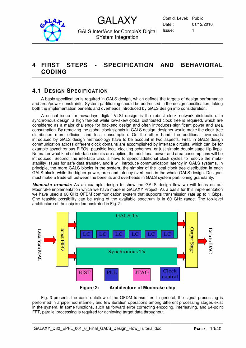
Moonrake example: As an example design to show the GALS design flow we will focus on our Moonrake implementation which we have made in GALAXY Project. As a basis for this implementation we have used a 60 GHz OFDM communication system that supports transmission rate up to 1 Gbps. One feasible possibility can be using of the available spectrum is in 60 GHz range. The top-level architecture of the chip is demonstrated in Fig. 2.
Input F
IFO
BIST
Synchronous Tx
GALS Tx
LC
1
LC
2
LC
3
LC
4
LC
5
LC
6
Outp
ut S
tage
PLL JTAG
Data fro
m M
AC
Data to
DA
C
Clock
control
Figure 2: Architecture of Moonrake chip
Fig. 3 presents the basic dataflow of the OFDM transmitter. In general, the signal processing is performed in a pipelined manner, and few iteration operations among different processing stages exist in the system. In some functions, such as forward error correcting encoding, interleaving, and 64-point FFT, parallel processing is required for achieving target data throughput.

GALAXY GALS InterfAce for CompleX Digital
SYstem Integration
Confid. Level:
Date :
Issue:
Public
01/12/2010
1
GALAXY_D32_EPFL_001_6_Final_GALS_Design_Flow_Tutorial.doc PAGE: 11/40
Figure 3: OFDM transmitter dataflow
An important step in the design of a GALS chip is a GALS partitioning. Criterions for efficient GALS system partitioning have been exploited in the Moonrake chip design:
a. Less interconnects across different GALS blocks. The more interface signals passing from one GALS block into another GALS block, the more overheads and less reliability in synchronization. It means that GALS system partitioning should basically follow in the functionality.
b. Average area and power contributions from each GALS block. Considering the overheads result by the synchronization circuits, a reasonable amount of GALS blocks are preferred. For each GALS block, the partitioning should lead to an average area or power consumptions, depending on the applications, to exploit the benefits of GALS design style.
The primary goal of Moonrake chip design is to exploit GALS design in low-EMI digital systems. Hence, the average power consumption among different GALS blocks is preferred. Table 1 shows the power consumption of each functional module in the system estimated using Synopsys PrimeTime (PT) based on the synthesized netlist of the synchronous design.
According to the power estimation of each functional module, system partitioning of the GALS OFDM transmitter is further performed, also shown in Table 1. It can be clearly seen here that: (1) the

GALAXY GALS InterfAce for CompleX Digital
SYstem Integration
Confid. Level:
Date :
Issue:
Public
01/12/2010
1
GALAXY_D32_EPFL_001_6_Final_GALS_Design_Flow_Tutorial.doc PAGE: 12/40
system partitioning is based on the functional modules, and (2) the power consumption from each GALS block is averaged in the system.
Table 1: Power Estimation and System partitioning of GALS OFDM Transmitter
GALS Block 1
Input
controller Symbol mapping
Universal scramble
r
Middle controller
FEC encoder
[12:1]
Output interface
Pilot insertion
Mapping [4:1]
Total
Power 0.1% 0.5% 0.0% 7.0% 0.09% 0.1% 3.1% 0.08% 10.97%
Area 0.1% 1.0% 0.0% 12.8% 0.06% 0.1% 5.1% 0.14% 19.3%
GALS Block 2 GALS Block 3 GALS Block 4
Interleav
e 1 Interleav
e 2 Total
Interleave3
Interleave 4
Total Interleav
e 5 Interleav
e 6 Total
Power 8.7% 8.7% 17.4% 8.7% 8.7% 17.4% 8.7% 8.7% 17.4%
Area 8.9% 8.9% 17.8% 8.9% 8.9% 17.8% 8.9% 8.9% 17.8%
GALS Block 5 GALS Block 6
FFT_64P
1 FFT_64P
2 FFT_64P
3 FFT_64P
4 Total FFT_4P Backend Total
GALS Block
Average
Power 4.9% 4.3% 4.3% 4.3% 17.8% 11.3% 7.2% 18.5% 50mW
Area 2.7% 2.4% 2.4% 2.4% 9.9% 10.3% 6.7% 17% 0.36mm2
Note: Synthesized using the IFX40lpsvt12 library at a working frequency of 200MHz
Total power consumption: 300mW (average) / 250W (peak)
Total area consumption: 2.14mm2 (synthesized)
4.2 BEHAVIOURAL LEVEL CODING
Two parts of behavioural level coding are included in GALS design. For synchronous functional modules, standard register-transfer-level (RTL) design is used, often programming in VHDL/Verilog or SystemC. However, for asynchronous circuits, which are involved, for example, in the pausible clocking scheme in asynchronous wrappers, particular languages are needed for behavioural level programming. In GALAXY project, signal transition graphs (STGs), which are based on petri net analysis, have been applied to describe the behaviour of asynchronous port controllers.
The RTL design for synchronous digital circuits is mature and well supported by commercial CAD tools. In GALS design, most of the circuits, including all the functional modules, are normally designed in synchronous manner. That means the behavioural level design of GALS systems is rather similar to the traditional synchronous systems in general. Asynchronous design is only used for the interface circuits in GALS design. Considering the simple structures of interface circuits, asynchronous design in GALS systems only occupy a very limit part in the system design efforts. For the simple asynchronous circuits, the behavioural level design methods mentioned above is efficient and easy for application.
Moonrake example: Fig. 4 illustrates the topology of the GALS OFDM transmitter. It can be seen that a star-like topology is applied in the design. GALS_Block_1 works as a central manage block, including most of the global control logic and scheduling the working status of the other five GALS blocks.
In Moonrake chip design, the pausible clocking based GALS design is applied. A local clock generator is deployed in each GALS block, which provides the clock pulses for all the locally synchronous modules inside the GALS block and can be programmed at frequency.

GALAXY GALS InterfAce for CompleX Digital
SYstem Integration
Confid. Level:
Date :
Issue:
Public
01/12/2010
1
GALAXY_D32_EPFL_001_6_Final_GALS_Design_Flow_Tutorial.doc PAGE: 13/40
The communication between different GALS blocks is performed by channels controlled each by a pair of input and output asynchronous port controllers. A total of 16 communication channels (32 input and output ports) are utilized among the 6 GALS blocks in the system.
Considering the pipelined dataflow rooted in the OFDM transmitter, all the GALS blocks are configured to be running at the same frequency, with tiny frequency shifting caused by fabrication and environment uncertainty. Therefore, it actually works as a metachronous GALS system.
Figure 4: Topology of GALS OFDM transmitter
Basically, the RTL design of synchronous functional modules in GALS systems is the same to that of synchronous digital circuits design. However, for pausible clocking based GALS design, the following design rules need to be taken into consideration in synchronous RTL coding:
a. All the input and output signals of GALS blocks need to be registered by flip-flops. Normally only the output data has to be registered in synchronous RTL design to minimize the uncertainty of output delay with respect to the trigger edge of clock. However, in the pausible clocking based GALS design, the top-level input signals, signals from other GALS blocks or from the external environment, should be also registered in flip-flops before used in the GALS block. This design style is mainly to guarantee sufficient timing margins for the interconnect delays of the top-level input signals, which are asserted by the asynchronous input port macros. A larger acceptable interconnect delay means less constraints in the placement and routing in backend design.
b. An additional cycle needs to be left as synchronization timing margin for control signals across GALS blocks. In pausible clocking GALS design, the input signals could be valid either in the current clock cycle or in the immediately following clock cycle, depending on the arrival time of the input signals and the acknowledge window of pausible clock generator, and maximum one cycle synchronization delay can be introduced [FAN09]. As a consequence, any control signal transferred from other GALS blocks should be asserted one cycle earlier before the status. For example, empty and full flags are usually generated to identify the status of asynchronous FIFO in synchronous RTL design, however, if these flags need to be transferred across GALS blocks in GALS design, then errors could be introduced. Once the flags were received one cycle later than it was asserted. Instead, underflow or overflow could occur in FIFO. Instead, almost_empty

GALAXY GALS InterfAce for CompleX Digital
SYstem Integration
Confid. Level:
Date :
Issue:
Public
01/12/2010
1
GALAXY_D32_EPFL_001_6_Final_GALS_Design_Flow_Tutorial.doc PAGE: 14/40
and almost_full flags should be used in GALS design, in which the flags are asserted when at least one data or spaces remaining in the FIFO to be read or written.
Above states the design rules specific to the GALS design in Moonrake chip. In comparison with the synchronous design, fewer design efforts or implantation overheads in area and power consumption are introduced by the GALS design.
In Moonrake chip design, a set of asynchronous input and output (I/O) port controllers are utilized for signal synchronization across different GALS block. Since the I/O port controllers are relatively simple in behaviour, the signal transition graphs (STGs) are applied to describe the I/O ports controllers, shown in Fig. 5.
Both two-phase (transition sensitive) and four-phase (level sensitive) handshaking protocols are utilized in the I/O port controllers. To minimize the handshaking latency caused by long interconnect between I/O port macros and synchronous functional modules, two-phase protocol is adopted on the pair of port request/acknowledge (Rp/Ap) and transfer enable/acknowledge (Te/Ta). On the other hand, four-phase protocol is applied on the pair of internal request/acknowledge (Ri/Ai) to indicate the status of local clock.
Figure 5: STG of asynchronous I/O port controllers

GALAXY GALS InterfAce for CompleX Digital
SYstem Integration
Confid. Level:
Date :
Issue:
Public
01/12/2010
1
GALAXY_D32_EPFL_001_6_Final_GALS_Design_Flow_Tutorial.doc PAGE: 15/40
5 GALAXY DESIGN TOOLS UNDER GPL
The behavioural level descriptions of both synchronous functional modules and asynchronous wrappers have to be integrated in a complete environment for system simulations. An asynchronous-synchronous co-simulation tool GALAXY-IDE, using ASIP packaging format, is developed in the GALAXY project, which supports behaviour level co-simulation using different languages such as VHDL/Verilog, SystemC and STG/Petri-Net, and provides an effective approach to cover the behavioural design of synchronous-asynchronous interfacing circuits in early design stage.
5.1 ASYNCHRONOUS-SYNCHRONOUS CO-SIMULATION
Including the asynchronous circuits in behavioural level simulations is crucial for GALS systems design. Although the structures of asynchronous interface circuits are relatively simple, their behaviour could be very complicated. The output response of asynchronous circuits is influenced both by the transitions on input signals and by the sequence of transitions appearing on input signals. Same combination of input transitions with different timing sequences could lead to different outputs from the asynchronous circuits. Generally speaking, the input signals arrive randomly in GALS interface circuits, and it turns out to be of importance to cover all the corner cases in the high-level behavioural simulations. ASIP provides a solution to perform the behavioural-level asynchronous-synchronous co-simulations. Up to now, it is the only tool supporting the system-level behavioural simulations of GALS designs.
We focus on the FFT section of the baseband processor, and show how the GALAXY design tools can be used to process it iteratively, using various co-simulations to validate the new design at each iteration.
5.2 PROJECT IMPORT IN GALAXY TOOLS
The GALAXY design tools are built around the ASIP file format, an XML specification format developed as part of the GALAXY project, and able to describe IPs in a hierarchical way at multiple levels of abstractions and mixing synchronous and asynchronous components (described in deliverable D19).
Several “project wizards” have been developed: VHDL2ASIP, Verilog2ASIP, PNML2ASIP (Petri Net Markup Language), STG2ASIP (Signal Transition Graph).
The original baseband processor being described in VHDL, the VHDL2ASIP tool can be used to generate a baseband processor ASIP project.
5.2.1 VHDL2ASIP
Running the following command in the base directory of the Baseband processor VHDL source code generates the corresponding ASIP project:
vhdl2asip.sh –d . –t hwtx_tb
The file hwtx_tb.asip.xml is generated, and can be explored thanks to our main graphical design tool: AsipIDE.
5.2.2 AsipIDE asipide –i hwtx_tb.asip.xml
The generated ASIP file can be viewed in AsipIDE, but hasn’t gone through any layout process yet,
as shown in Figure 6.

GALAXY GALS InterfAce for CompleX Digital
SYstem Integration
Confid. Level:
Date :
Issue:
Public
01/12/2010
1
GALAXY_D32_EPFL_001_6_Final_GALS_Design_Flow_Tutorial.doc PAGE: 16/40
Figure 6: Initial view of the baseband processor in AsipIDE
The initial conversion doesn’t include any automatic layout, but this option is then available inside the IDE.
After a manual reorganisation of the components using the graphical editor, we achieve a
representation similar to the hand-drawn one, as shown in Figure 7 and Figure 8.

GALAXY GALS InterfAce for CompleX Digital
SYstem Integration
Confid. Level:
Date :
Issue:
Public
01/12/2010
1
GALAXY_D32_EPFL_001_6_Final_GALS_Design_Flow_Tutorial.doc PAGE: 17/40
Figure 7: Reorganised view of the baseband processor in AsipIDE
The advantage of an online interface compared to hand-drawn pictures is the ability to navigate
inside the design: expanding/hiding groups, zooming in/out. Figure 8 shows the main part of the Baseband processor design in more details (and with connections hidden). This actually looks very similar to the diagrams used in published papers, and is therefore very useful for interactive presentations.
Figure 8: AsipIDE navigation capabilities
From here, we will focus on the FFT section of the baseband processor, shown in Figure 9. The colours and layout were chosen to match those from the published papers from IHP.

GALAXY GALS InterfAce for CompleX Digital
SYstem Integration
Confid. Level:
Date :
Issue:
Public
01/12/2010
1
GALAXY_D32_EPFL_001_6_Final_GALS_Design_Flow_Tutorial.doc PAGE: 18/40
Figure 9: Focus on FFT module
5.3 S IMULATION
By default, vhdl2asip will have associated each component with the Modelsim simulator. Assuming that the Modelsim simulation back-end is properly configured, the simulation can be run from AsipIDE just by clicking the “Run Simulation” icon or menu entry.
As shown in Figure 10, two windows should appear: the Tool Flow window and the Execution window. The Execution window should go through all the compilation stages and finally run Modelsim in console mode.

GALAXY GALS InterfAce for CompleX Digital
SYstem Integration
Confid. Level:
Date :
Issue:
Public
01/12/2010
1
GALAXY_D32_EPFL_001_6_Final_GALS_Design_Flow_Tutorial.doc PAGE: 19/40
Figure 10: Modelsim simulation views
The coloured lines in the Execution window represent parallel threads execution. Here they correspond to the compilation of each VHDL file.
The simulation generates a VCD trace file, which is parsed by AsipIDE while the simulation is
running. The Simulation View updates itself regularly and shows the current simulation time.
One of the main features of the GALAXY framework is its ability to represent the simulation events as an animation over time. Clicking “Animate” or changing the currently shown time step in the Simulation View colourises and animates (through colour changes) the connections between
components in the Graph View to show the state of each wire at the specified time step (Figure 11 shows one time step of the animation).

GALAXY GALS InterfAce for CompleX Digital
SYstem Integration
Confid. Level:
Date :
Issue:
Public
01/12/2010
1
GALAXY_D32_EPFL_001_6_Final_GALS_Design_Flow_Tutorial.doc PAGE: 20/40
Figure 11: Simulation events mapped on Graph View connections
This VHDL simulation and representation of the VCD trace file are an important first step, but the importance of our framework lies in its handling of co-simulations, illustrated in the next section.
5.4 CO-SIMULATIONS
The GALAXY framework allows for any number of simulators to be connected together, and any language simulator can easily be supported by our toolkit. At the time of writing, the following languages are integrated in the possible co-simulations: SystemC, Verilog, VHDL, Petri nets and STGs.
Simulating HDLs such as Verilog/VHDL and SystemC with small modules described by Petri nets or STGs is important for asynchronous design, and this is made easy by the GALAXY tools. The next section presents VHDL-STG co-simulation.
5.4.1 VHDL-STG co-simulation
In each GALS block, 3 GALS components are present:
• PI port, handling the inputs of the GALS block;
• DO port, handling the outputs of the GALS block;
• the lower component, made of plausible clock generator and phase frequency modulator.
The main descriptions of the PI and DO ports in the original Baseband processor/FFT project are Signal
Transition Graphs (STG), shown in Figure 12.

GALAXY GALS InterfAce for CompleX Digital
SYstem Integration
Confid. Level:
Date :
Issue:
Public
01/12/2010
1
GALAXY_D32_EPFL_001_6_Final_GALS_Design_Flow_Tutorial.doc PAGE: 21/40
Figure 12: Original STG of GALS components DO and PI
In this example, the PI component’s STG was converted to ASIP by the stg2asip tool, and
integrated in the current project as a new implementation of the PI_port component. Figure 13 shows the representation of the converted STG in Asip-IDE.
Figure 13: STG in ASIP and co-simulation STG-VHDL
The STG is actually converted to ASIP in a different way than other languages: whereas VHDL or Verilog descriptions have to be split into two parts - the structural hierarchy of components and the behavioural code - STG don’t have any behavioural part. They can therefore be entirely converted to
GALAXY GALS InterfAce for CompleX Digital
SYstem Integration
Confid. Level:
Date :
Issue:
Public
01/12/2010
1
GALAXY_D32_EPFL_001_6_Final_GALS_Design_Flow_Tutorial.doc PAGE: 22/40
ASIP, which helps in several respects. The most important benefit is the efficient co-simulation of STG with other HDL.
Running the co-simulation is similar to the VHDL-only simulation: clicking on the “Run Simulation”, “Update Trace” and “Animate” buttons leads to the connections being animated based on the simulation trace events.
5.5 SUMMARY
Including asynchronous controllers in behavioural level simulations is crucial for GALS systems design. The GALAXY tools support behaviour level co-simulation using different languages such as VHDL/Verilog, SystemC and STG/Petri-Net, and provide an effective approach to cover the behavioural design of synchronous-asynchronous interfacing circuits in early design stages. ASIP provides a solution to perform the behavioural-level asynchronous-synchronous co-simulations. Up to now, it is the only tool supporting the system-level behavioural simulations of GALS designs.
We have demonstrated the use of the GALAXY tools for the co-simulation and visualisation of the STG GALS controllers and the VHDL description of IHP’s baseband processor, by focusing on the FFT module.

GALAXY GALS InterfAce for CompleX Digital
SYstem Integration
Confid. Level:
Date :
Issue:
Public
01/12/2010
1
GALAXY_D32_EPFL_001_6_Final_GALS_Design_Flow_Tutorial.doc PAGE: 23/40
6 AUTOMATION OF SYNTHESIS FLOW FOR GALS
6.1 SYNTHESIS
Asynchronous and synchronous behavioural coding are synthesized using different CAD tools separately in GALS design. For synchronous RTL coding, Synopsys Design Compiler (DC) could be utilized in digital circuits synthesis using standard cells library. The synthesis of asynchronous behavioural coding is much challenging than its synchronous counterpart. Particular CAD tools, such as BALSA, TAST, HASTE for complicated asynchronous circuits or Petrify, 3D, Minimalist for simple asynchronous logic, are used to guarantee the quasi-delay-insensitivity (QDI) of the gate-level circuits.
Muller-C element and Mutual Exclusive element (MUTEX) are widely applied in asynchronous design, however, these cells are not included in most of nowadays synchronous standard cells library. Efforts are therefore required to create an asynchronous standard cells library using the same technology to the synchronous standard cells library. Because only a few types of asynchronous cells are needed in GALS design, the generation of asynchronous library is relatively simple.
Asynchronous parts in GALS design need to be synthesized separately from the synchronous circuits. The netlist of synthesized asynchronous circuits is sensitive to the environment variations, such as the input signal transition time and output signal fan-out loads. To correctly set I/O constraints for asynchronous circuit synthesis, a careful estimation on the environment is required. On the other hand, the synthesis of synchronous modules in GALS design is similar to the synchronous design.
Moonrake example: Since the performance and reliability of asynchronous circuits are sensitive to the interconnect delay, in GALS OFDM transmitter design, hierarchical synthesis is performed. The functional modules from all the GALS blocks are synthesized as multi-clock synchronous design, while local clock generators and asynchronous ports are synthesized separately.
The synchronous functional modules from all the GALS blocks are synthesized as a synchronized core. Because each GALS block has different local clock signal, it is indeed the synthesis of a multiple clock design. Therefore, the main point is the definition and declaration of true paths and false paths between clock domains. Fig. 12 clearly demonstrated the clock dependency in the GALS OFDM transmitter. Besides the clock signals GALS_BLK[1-6]_CLK created by local clock generators in GALS blocks, two external clock signals, CLK_JTAG and CLK_EXTW, are used for programmable registers configuration and final output data buffering, respectively. Data latching registers of input ports are integrated in the synchronized core. Clock signals, ACK and GNT, are asserted by the asynchronous wrapper for triggering the input port registers.

GALAXY GALS InterfAce for CompleX Digital
SYstem Integration
Confid. Level:
Date :
Issue:
Public
01/12/2010
1
GALAXY_D32_EPFL_001_6_Final_GALS_Design_Flow_Tutorial.doc PAGE: 24/40
Figure 14: Clock dependency in GALS OFDM transmitter
Since there is no global clock reference in the asynchronous circuits, the switching of combinational and sequential gates are both triggered by the local signal pulses. As a result, any glitch on the internal wires could lead to mal-function of the whole design. That means the synthesis of asynchronous circuits is much challenging than that of synchronous counterpart.
The ideal design should be insensitive to both gate delays and wire delays, which is referred to as delay insensitive (DI) design. Unfortunately, it is proven that only rather simple logic could satisfy DI property. Instead, quasi-delay-insensitive (QDI) circuits are developed, where the design is robust with respect to any gate and wire delays if only the isochronic forks are used [SF01]. In Moonrake chip design, the STG of asynchronous port controllers are synthesized using Petrify to guarantee the QDI property of the gate-level circuits.
Fig. 13 illustrates the netlist of I/O port controllers synthesized using Petrify. It can be seen that both I/O port controllers have rather simple structures, introducing very few overheads in area and power consumption. To satisfy the isochronic property in the forks which is required by QDI design, the layout of those structures turns to be critical.
For implementation of the synchronous and asynchronous part of the circuit we have used standard low power 40 nm library from Infineon supplemented by additional asynchronous cell set, as defined in deliverable D4. Actually, the additional components (mutex, C-element) were only needed for

GALAXY GALS InterfAce for CompleX Digital
SYstem Integration
Confid. Level:
Date :
Issue:
Public
01/12/2010
1
GALAXY_D32_EPFL_001_6_Final_GALS_Design_Flow_Tutorial.doc PAGE: 25/40
the core of the pausible clocking generator. For the other components, the standard cell library is fully used.
Figure 15: Synthesized netlist of I/O port controllers using Petrify
6.1.1 Timing Constraints in Moonrake Chip Design
The timing issues in Moonrake design are complicated. Hierarchical synthesis and layout have been performed to achieve the target timing requirements. In the following, we will descript the key timing constraints in the GALS design.
Timing constraints in pausible clock generators
The structure of pausible clock generators used in the GALS design is shown in Fig. 14. As we can see here it in principle consists of a number of delay lines with some combinational control logic. The delay lines are simply made of a series of inverters, and are implemented as hard macros to control the electronics characteristics. Based on the hard macro of delay lines, the implementation of pausible clock generator is relatively easy to handle. In particular, as a clock source module, maximum fanout and maximum transition time constraints need to be set here to minimize its interconnect delays, and sufficient driving strength is also required to provide fast transition clock signals. Important constraints in pausible clock generators are shown below for reference.
Figure 16: The structure of pausible clock generator
set_driving_cell -library SLOWLIB.db: LIB -lib_cell NAND -pin Z -
input_transition_rise 0.16 -from_pin A -no_design_rule [get_ports "REQ nRSTI
SYNCEND"]
set pin_cap [load_of [get_lib_pins LIB/NAND/A]]
set_load [expr 16 * $pin_cap] [all_outputs]
set_max_fanout 4 LCLKGEN

GALAXY GALS InterfAce for CompleX Digital
SYstem Integration
Confid. Level:
Date :
Issue:
Public
01/12/2010
1
GALAXY_D32_EPFL_001_6_Final_GALS_Design_Flow_Tutorial.doc PAGE: 26/40
set_max_transition 0.08 LCLKGEN
Timing constraints in asynchronous port controllers
Similar to the pausible clock generator, constraints on the maximum fanout, transition time and output loads are set on the port controllers, as shown below.
set_driving_cell -library SLOWLIB.db:LIB -lib_cell NAND -pin Z -
input_transition_rise 0.16 -from_pin A -no_design_rule [all_inputs]
set pin_cap [load_of [get_lib_pins LIB/NAND/A]]
set_load [expr 16 * $pin_cap] [all_outputs]
set_max_fanout 4 PINTRANS2PHASE
set_max_transition 0.08 PINTRANS2PHASE
For the input port controller, the propagation delays on the following paths from input ports to output ports need to be minimized. The delays from RP to RI and from AI to AP significantly affect the latency of data transfer in input port controller. However, the delay from AI to TA is more critical, since a large propagation delay in this path could lead to setup timing violations in the data detection logic in the receiver side. For the output port controller, there is no special constraint on path delay.
set_max_delay 0.30 -from [get_ports RP] -to [get_ports RI]
set_max_delay 0.30 -from [get_ports AI] -to [get_ports AP]
set_max_delay 0.25 -from [get_ports AI] -to [get_ports TA]
The port allocation in the hard macros of I/O port controllers is of importance. There are seven external ports in both output port controller and input port controller, including six asynchronous functional signals working as three handshaking pairs and one asynchronous active-low reset signal. Each pair of handshake pins needs to be located on the same side of the hard macros to minimize the interconnect delay. An example of the pin allocation on the hard macros of asynchronous port controllers is illustrated in Fig. 15.
Figure 17: Port allocation of I/O port controllers
Timing constraints in the core logic of GALS design
There are in total six GALS blocks in the GALS design. Each GALS block is triggered by a local clock signal, and two handshaking clocks are used to latch the data in the double-latching input mechanism. Fig. 16 demonstrates the data transfer scheme between a pair of GALS blocks. The main challenge here is to clearly define the clock signals and their correlations between each other.

GALAXY GALS InterfAce for CompleX Digital
SYstem Integration
Confid. Level:
Date :
Issue:
Public
01/12/2010
1
GALAXY_D32_EPFL_001_6_Final_GALS_Design_Flow_Tutorial.doc PAGE: 27/40
Figure 18: Data transfer across GALS blocks
Local Clock Declarations
Same to the synchronous design, the target working frequency of GALS design is 160MHz. However, in order to support the clock frequency modulation (+-0.6ns) in GALS mode for low-EMI features, also taking into account the intrinsic jitters on local clock signals from ring oscillators, the clock period in GALS design is set to be 5.4ns, corresponding to a maximum frequency of 185MHz. Even with such an aggressive timing constraint, the GALS design are synthesized and layout successfully. In contrast, due to the large clock fan-out in the synchronous design, the synchronous design could be synthesized with a clock period of 6.25ns at most. By this means, we can achieve the same average frequency in the GALS mode with clock modulation as in the synchronous mode. Moreover, it is very possible that the chip would be working at a much higher frequency in GALS mode without clock modulation than the synchronous mode, leading to an increase in data throughput. The definition of GALS local clock signals are presented below.
create_clock [get_pins tx_gals_sync_inst/GALSTX/u_GalsBlk?/u_gals_blk?_lclkgen/CLKO] –name GALS_BLK?_CLK -period 5.4 -waveform {0 2.7}
set_clock_latency -max 1 [get_clocks GALS_BLK?_CLK]
set_clock_latency -min 0.5 [get_clocks GALS_BLK?_CLK]
set_clock_uncertainty -setup 0.3 [get_clocks GALS_BLK?_CLK]
set_clock_uncertainty -hold 0.2 [get_clocks GALS_BLK?_CLK]
set_clock_transition -rise 0.16 [get_clocks GALS_BLK?_CLK]
set_clock_transition -fall 0.16 [get_clocks GALS_BLK?_CLK]
set_clock_transition -min -rise 0.06 [get_clocks GALS_BLK?_CLK]
set_clock_transition -min -fall 0.06 [get_clocks GALS_BLK?_CLK]
Handshaking Clock Declarations
Besides the local clock signals, the handshaking signals, ACK and GNT, from the pausible clock generators are also used as the clock signals to trigger the double-stage input flip-flops in the data receiving GALS block. Different from the local clock signals, these handshaking signals are pretty narrow in the pulse width, while normally they have only limited fan-out loads. The definition of handshaking clock signals is shown as follows for example.
create_clock [get_pins {tx_gals_sync_inst/GALSTX/u_GalsBlk?/u_gals_blk?_lclkgen/ACK[*]}] -name GALS_BLK?_ACK[*] -period 1 -waveform {0 0.5}
set_clock_latency -max 0.1 [get_clocks {GALS_BLK?_ACK[*]}]
set_clock_latency -min 0 [get_clocks {GALS_BLK?_ACK[*]}]
GALAXY GALS InterfAce for CompleX Digital
SYstem Integration
Confid. Level:
Date :
Issue:
Public
01/12/2010
1
GALAXY_D32_EPFL_001_6_Final_GALS_Design_Flow_Tutorial.doc PAGE: 28/40
set_clock_uncertainty -setup 0.3 [get_clocks {GALS_BLK?_ACK[*]}]
set_clock_uncertainty -hold 0.2 [get_clocks {GALS_BLK?_ACK[*]}]
set_clock_transition -rise 0.16 [get_clocks {GALS_BLK?_ACK[*]}]
set_clock_transition -fall 0.16 [get_clocks {GALS_BLK?_ACK[*]}]
set_clock_transition -min -rise 0.06 [get_clocks {GALS_BLK?_ACK[*]}]
set_clock_transition -min -fall 0.06 [get_clocks {GALS_BLK?_ACK[*]}]
create_clock [get_pins {tx_gals_sync_inst/GALSTX/u_GalsBlk?/u_gals_blk?_lclkgen/GNT[*]}] -name GALS_BLK?_ GNT [*] -period 1 -waveform {0 0.5}
set_clock_latency -max 0.3 [get_clocks {GALS_BLK?_ GNT [*]}]
set_clock_latency -min 0.2 [get_clocks {GALS_BLK?_ GNT [*]}]
set_clock_uncertainty -setup 0.3 [get_clocks {GALS_BLK?_ GNT [*]}]
set_clock_uncertainty -hold 0.2 [get_clocks {GALS_BLK?_ GNT [*]}]
set_clock_transition -rise 0.16 [get_clocks {GALS_BLK?_ GNT [*]}]
set_clock_transition -fall 0.16 [get_clocks {GALS_BLK?_ GNT [*]}]
set_clock_transition -min -rise 0.06 [get_clocks {GALS_BLK?_ GNT [*]}]
set_clock_transition -min -fall 0.06 [get_clocks {GALS_BLK?_ GNT [*]}]
GALS Clock Correlation Declarations
To sample the input data successfully, certain timing correlations between the local clock signals and handshaking clock signals need to be satisfied. Firstly, to guarantee the correct sampling sequence after layout, the clock tree of ACK, GNT, and CLK should be carefully inserted meeting the following constraint on the minimum clock tree insertion delays:
clock_latency –min ACK <clock_latency –min GNT < clock_latency –min CLK.
Secondly, with above restriction, all the paths across different clock domains should be set as false path as shown below to avoid timing check. The timing issues on those clocks are addressed in the design of clock generators and port controllers.
set_false_path -from [get_clocks GALS_BLK?_ACK[*]] –to [get_clocks GALS_BLK?_GNT[*]]
set_false_path -from [get_clocks GALS_BLK?_GNT[*]] –to [get_clocks GALS_BLK?_CLK]
set_false_path -from [get_clocks GALS_BLK?_CLK] –to [get_clocks GALS_BLK?_ACK[*]]
set_false_path -from [get_clocks GALS_BLK?_CLK] –to [get_clocks GALS_BLK?_GNT[*]]
GALS Timing constraints on system-level integration
The timing constraints on the top-level integration are to define the timing issues of global signals used in the GALS design and to specify the timing requirements on the handshaking signals between hard macros and core logic.
I/O Constraints
As shown in Fig. 17, the communication between GALS design and the synchronous environment is via GALS block 1 and GALS block 6 only. So the constraints are relatively simple.

GALAXY GALS InterfAce for CompleX Digital
SYstem Integration
Confid. Level:
Date :
Issue:
Public
01/12/2010
1
GALAXY_D32_EPFL_001_6_Final_GALS_Design_Flow_Tutorial.doc PAGE: 29/40
Figure 19: Communication scheme between GALS design and outside
set_false_path -from [get_clocks GALS_BLK6_CLK] -to [get_clocks CLK_PLLO]
set_false_path -from [get_clocks GALS_BLK6_CLK] -to [get_clocks CLK_EXTW]
set_false_path -from [get_clocks GALS_BLK6_CLK] -to [get_clocks CLK_JTAG]
set_false_path -from [get_clocks CLK_PLLO] -to [get_clocks GALS_BLK6_CLK]
set_false_path -from [get_clocks CLK_JTAG] -to [get_clocks GALS_BLK6_CLK]
set_false_path -from [get_clocks CLK_EXTW] -to [get_clocks GALS_BLK6_CLK]
set_false_path -from [get_clocks GALS_BLK1_CLK] -to [get_clocks CLK_PLLO]
set_false_path -from [get_clocks GALS_BLK1_CLK] -to [get_clocks CLK_EXTW]
set_false_path -from [get_clocks GALS_BLK1_CLK] -to [get_clocks CLK_JTAG]
set_false_path -from [get_clocks CLK_PLLO] -to [get_clocks GALS_BLK1_CLK]
set_false_path -from [get_clocks CLK_JTAG] -to [get_clocks GALS_BLK1_CLK]
set_false_path -from [get_clocks CLK_EXTW] -to [get_clocks GALS_BLK1_CLK]
set_output_delay -clock GALS_BLK6_CLK -max 2 [get_ports {i1[*]}]
set_output_delay -clock GALS_BLK6_CLK -min 0 [get_ports {i1[*]}]
set_output_delay -clock GALS_BLK6_CLK -max 2 [get_ports {q1[*]}]
set_output_delay -clock GALS_BLK6_CLK -min 0 [get_ports {q1[*]}]
Timing Constraints on Handshaking Signals
One of the most challenging tasks in Moonrake design is to correctly specify the timing requirements of the handshaking signals between the pausible clock generators and asynchronous port controllers and the core logic. This timing information will dominate the placement of the hard macros and affect significantly on the performance of GALS design.
The preferred placement of the hard macros according to the core logic is presented in Fig. 18. There are three handshaking channels used. For each data transfer, these signals need to accomplish one time of handshaking sequence. Therefore, the performance of GALS design to some extent depends on the speed of these handshaking channels rather than the working frequency.
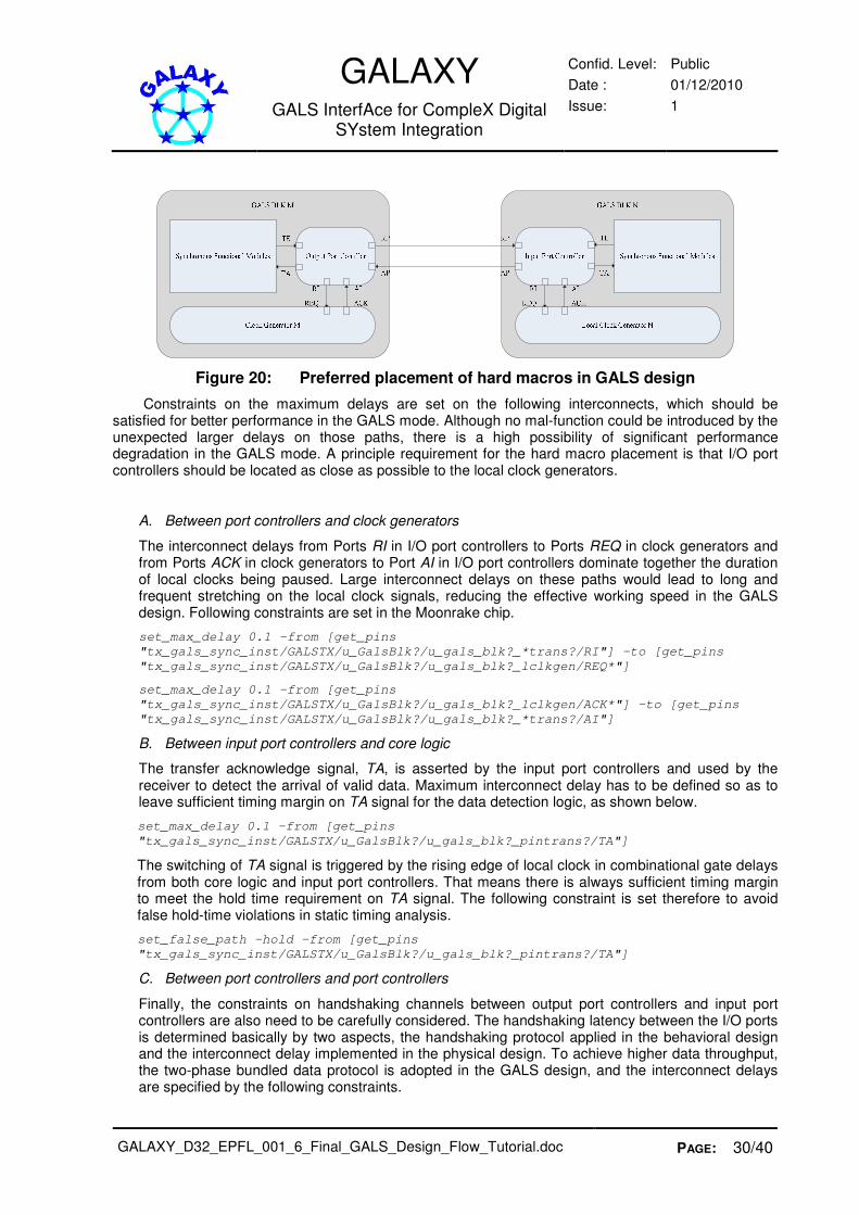
GALAXY GALS InterfAce for CompleX Digital
SYstem Integration
Confid. Level:
Date :
Issue:
Public
01/12/2010
1
GALAXY_D32_EPFL_001_6_Final_GALS_Design_Flow_Tutorial.doc PAGE: 30/40
Figure 20: Preferred placement of hard macros in GALS design
Constraints on the maximum delays are set on the following interconnects, which should be satisfied for better performance in the GALS mode. Although no mal-function could be introduced by the unexpected larger delays on those paths, there is a high possibility of significant performance degradation in the GALS mode. A principle requirement for the hard macro placement is that I/O port controllers should be located as close as possible to the local clock generators.
A. Between port controllers and clock generators
The interconnect delays from Ports RI in I/O port controllers to Ports REQ in clock generators and from Ports ACK in clock generators to Port AI in I/O port controllers dominate together the duration of local clocks being paused. Large interconnect delays on these paths would lead to long and frequent stretching on the local clock signals, reducing the effective working speed in the GALS design. Following constraints are set in the Moonrake chip.
set_max_delay 0.1 -from [get_pins
"tx_gals_sync_inst/GALSTX/u_GalsBlk?/u_gals_blk?_*trans?/RI"] -to [get_pins
"tx_gals_sync_inst/GALSTX/u_GalsBlk?/u_gals_blk?_lclkgen/REQ*"]
set_max_delay 0.1 -from [get_pins
"tx_gals_sync_inst/GALSTX/u_GalsBlk?/u_gals_blk?_lclkgen/ACK*"] -to [get_pins
"tx_gals_sync_inst/GALSTX/u_GalsBlk?/u_gals_blk?_*trans?/AI"]
B. Between input port controllers and core logic
The transfer acknowledge signal, TA, is asserted by the input port controllers and used by the receiver to detect the arrival of valid data. Maximum interconnect delay has to be defined so as to leave sufficient timing margin on TA signal for the data detection logic, as shown below.
set_max_delay 0.1 -from [get_pins
"tx_gals_sync_inst/GALSTX/u_GalsBlk?/u_gals_blk?_pintrans?/TA"]
The switching of TA signal is triggered by the rising edge of local clock in combinational gate delays from both core logic and input port controllers. That means there is always sufficient timing margin to meet the hold time requirement on TA signal. The following constraint is set therefore to avoid false hold-time violations in static timing analysis.
set_false_path -hold -from [get_pins
"tx_gals_sync_inst/GALSTX/u_GalsBlk?/u_gals_blk?_pintrans?/TA"]
C. Between port controllers and port controllers
Finally, the constraints on handshaking channels between output port controllers and input port controllers are also need to be carefully considered. The handshaking latency between the I/O ports is determined basically by two aspects, the handshaking protocol applied in the behavioral design and the interconnect delay implemented in the physical design. To achieve higher data throughput, the two-phase bundled data protocol is adopted in the GALS design, and the interconnect delays are specified by the following constraints.

GALAXY GALS InterfAce for CompleX Digital
SYstem Integration
Confid. Level:
Date :
Issue:
Public
01/12/2010
1
GALAXY_D32_EPFL_001_6_Final_GALS_Design_Flow_Tutorial.doc PAGE: 31/40
set_max_delay 0.2 -from [get_pins
"tx_gals_sync_inst/GALSTX/u_GalsBlk?/u_gals_blk?_douttrans?/RP"] -to [get_pins
"tx_gals_sync_inst/GALSTX/u_GalsBlk?/u_gals_blk?_pintrans?/RP"]
set_max_delay 0.2 -from [get_pins
"tx_gals_sync_inst/GALSTX/u_GalsBlk?/u_gals_blk?_pintrans?/AP"] -to [get_pins
"tx_gals_sync_inst/GALSTX/u_GalsBlk?/u_gals_blk?_douttrans?/AP"]
6.2 POST-SYNTHESIS S IMULATION
The netlist of both synchronous and asynchronous circuits are integrated in the top-level. The cell and interconnect delays are abstracted and back-annotated into the netlist for accurate gate-level simulations. Note that, since asynchronous circuits are synthesized independently, the delay information of asynchronous circuits relays on the I/O constraints set in synthesis. In top-level post-synthesis simulations, the variations on the delays of asynchronous circuits due to the mismatch between the constraints used for synthesis and the real value of the driving/load signals could lead to errors.
Moonrake example: We have used standard back-annotation methodology for the complete synthesized designs. Since we have as the output of the design process generated the common verilog netlist and common SDF file, standard simulation tool (Modelsim) was used to perform back-annotation.

GALAXY GALS InterfAce for CompleX Digital
SYstem Integration
Confid. Level:
Date :
Issue:
Public
01/12/2010
1
GALAXY_D32_EPFL_001_6_Final_GALS_Design_Flow_Tutorial.doc PAGE: 32/40
7 STRATEGIES FOR LAYOUT OF GALS CIRCUITS
7.1 BACK-END LAYOUT
The existing back-end tools do not support layout of asynchronous circuits. Existing problems in layout of GALS and generally asynchronous design are even more pronounced then in synthesis, since satisfying the isochronic property in the forks which is required by QDI design is layout critical. Time constraints basically restrict back-end of critical blocks to manual layout. There are some place&route efforts with existing CAD (synchronous) back-end tools [SOT02][NAJ07], where standard cell-based place&route is performed. Both works imply hierarchical place&route. [SOT02] relies on tighter synthesis constraints that provide correct operation even with small timing violations after place&route. This however implies higher delay penalties. In [NAJ07] parts of design that contain isochronic forks is isolated and is layout-ed separately using the provided templates. The rest of the design is place&routed using standard cell-based approach. In this way, the delay penalty is minimized, however the additional area penalty still remains high. Also, preparation of port templates increases significantly design effort.
In our approach we have also used hierarchical layout with the separation of critical and non-critical blocks. Considering the heavy sensitivity on performance and reliability to the interconnect delays, asynchronous circuits are best implemented as soft or hard macros. In system-level layout, these asynchronous macros are merged with other cells. Static timing analysis (STA) is done in both macro-level and system-level layout for timing closure. The approach has a benefit of both minimizing delay and area penalties.
Depending on the design requirements, the asynchronous circuits can be layout as soft-macros or hard-macros. As a soft macro, its timing information can be abstracted and used for post-layout simulations. As a hard macro, since it is layout in transistor level, it is difficult to abstract the delay information as normal digital cells for simulations. However, hard macro can be optimized with the maximum efforts for high performance and reliability. Moreover, it is possible to characterize hard macros in a similar way standard cells are characterized specifying delay tables for input/output pin pairs. This process can also be automated if all macro blocks use standard and relatively small number of pins.
Moonrake example: Hierarchical layout is performed in the design of GALS OFDM transmitter. The layout of pausible clock generators as well as the asynchronous port controllers is done separately from that of the functional modules. By this means, the cells in the asynchronous wrappers are placed as tightly as possible and the interconnect delays are controllable and minimized, contributing to the improvement in performance and reliability of asynchronous wrappers. The layout asynchronous wrappers are further integrated as soft macros in the top-level layout with the standard cells used in the synchronous netlist of functional modules. Commercial tools, such as Synopsys IC Compiler, are used in the design of GALS OFDM transmitter, and no effort is required for the development of CAD tools for GALS design layout.
The layout of asynchronous wrappers is relatively easy due to the simple structures of both pausible local clock generators and asynchronous I/O port controllers as shown in previous sections. To achieve better performance after layout, maximum fanout and maximum transition time constraints are set for the layout of asynchronous wrappers. Especially, constraints on the maximum delay are also asserted in the asynchronous port controllers. For example, some typical timing constraints used in the layout of asynchronous wrappers are shown below.
set_max_fanout 4 PINTRANS2PHASE
set_max_transition 0.08 PINTRANS2PHASE
set_max_delay 0.25 -from [get_ports AI] -to [get_ports TA]

GALAXY GALS InterfAce for CompleX Digital
SYstem Integration
Confid. Level:
Date :
Issue:
Public
01/12/2010
1
GALAXY_D32_EPFL_001_6_Final_GALS_Design_Flow_Tutorial.doc PAGE: 33/40
At the top-level layout, the most important issue is the minimization of the interconnect delays between lclock generators and I/O ports, I/O ports and synchronous modules, and the I/O port pairs consisting of communication channels. Therefore, the placement of soft macros is of crucial importance for system performance. First, port macros have to be located as close as possible to the corresponding clock generator. Second, the I/O ports handshaking with each other should be proximate as well. Third, the input ports have to be placed near to the GALS blocks where the input data is consumed.
To guide the layout tool following above placement criterions, a set of complex timing constraints has to be applied in the layout, listed below for instance.
set_max_delay 0.1 -from [get_pins
"tx_gals_sync_inst/GALSTX/u_GalsBlk?/u_gals_blk?_*trans?/RI"] -to [get_pins
"tx_gals_sync_inst/GALSTX/u_GalsBlk?/u_gals_blk?_lclkgen/REQ*"]
set_max_delay 0.1 -from [get_pins
"tx_gals_sync_inst/GALSTX/u_GalsBlk?/u_gals_blk?_lclkgen/ACK*"] -to [get_pins
"tx_gals_sync_inst/GALSTX/u_GalsBlk?/u_gals_blk?_*trans?/AI"]
set_max_delay 0.2 -from [get_pins
"tx_gals_sync_inst/GALSTX/u_GalsBlk?/u_gals_blk?_douttrans?/RP"] -to [get_pins
"tx_gals_sync_inst/GALSTX/u_GalsBlk?/u_gals_blk?_pintrans?/RP"]
set_max_delay 0.2 -from [get_pins
"tx_gals_sync_inst/GALSTX/u_GalsBlk?/u_gals_blk?_pintrans?/AP"] -to [get_pins
"tx_gals_sync_inst/GALSTX/u_GalsBlk?/u_gals_blk?_douttrans?/AP"]
set_max_delay 0.1 -from [get_pins
"tx_gals_sync_inst/GALSTX/u_GalsBlk?/u_gals_blk?_pintrans?/TA"]
The die microphotograph of the Moonrake chip after layout is demonstrated in Fig. 19. Post-layout simulations show that all the performance targets have been achieved by the design.
Figure 21: Final layout of Moonrake chip
7.2 POST-LAYOUT S IMULATION
Post-layout simulations are especially important to verify the functions of asynchronous circuits. For most of the asynchronous circuits, QDI property is preferred, where the circuits are robust to cell and isochronic wire delays. In post-synthesis simulation, however, there is no timing information on the wires. Only with the post-layout netlist, the interconnect delays in the asynchronous circuits could be

GALAXY GALS InterfAce for CompleX Digital
SYstem Integration
Confid. Level:
Date :
Issue:
Public
01/12/2010
1
GALAXY_D32_EPFL_001_6_Final_GALS_Design_Flow_Tutorial.doc PAGE: 34/40
checked. By implementing asynchronous circuits as macros in GALS systems, the interconnect delays can be fully controlled in the sense that after place&route it could be safely neglected.
Moonrake example: In the Moonrake example we have used standard flow for post-layout simulation. Top level design was back annotated for two edge corners (worst case and best case). Additionally, hard macros were separately annotated mainly based on the gate level delays. Important lesson that we have learned is that for the asynchronous components either one should use soft macros and than annotation is no problem or hard macros but than they have to be characterized as any other standard cell. In the Moonrake design hard macros were not fully characterized, due to the timing pressure, and that created significant risk for the operation of the system. For the next GALS implementation we would probably focus on soft macros because the effort is significantly lower for their timing annotation.
7.3 S IGN-OFF AND TAPE-OUT
As synchronous design, after passing DRC, LVS, etc. checking, the GALS design will be released for tape-out. The tools that should be used are standard commercial CAD tools used also for the synchronous designs.
Moonrake example: Standard flow was used to sign off of the Moonrake chip. ERC, DRC and LVS analysis was performed. After correcting some of the DRCs another run of timing closure is done and back annotated simulation was performed.

GALAXY GALS InterfAce for CompleX Digital
SYstem Integration
Confid. Level:
Date :
Issue:
Public
01/12/2010
1
GALAXY_D32_EPFL_001_6_Final_GALS_Design_Flow_Tutorial.doc PAGE: 35/40
8 GALS TEST FLOW
In order to apply the GALS methodology, we need a clear path how to test such structured systems. As soon as a design using self-timed circuit techniques is mentioned, the first question that pops up is: "How are you going to test this circuit?" This section summarizes recommendations on test development for GALS. The guidelines have been documented in detail in D16 which deals with the test methodology on GALS, and here we provide the most important excerpt.
• Use scan approach wherever this seems to be feasible and possible
Create one or more scan-path to reach all latches or flip-flops together of the synchronous parts. The scan-path may operate only when the circuit is in the test mode and can be generated by tools for synchronous designing. Automate test pattern generation tools can therefore be applied in order to minimize the test time and maximize the fault coverage. An external clock is needed in order the shift the states of the scan-path. Reasonable approach would be that each LS block has its autonomous scan chain(s). However, it is also possible to combine different LS domains into the single scan chain. In any case we can apply any of the scan methods that are anyway used for multi-clocking systems. Asynchronous wrappers could be included into scan chain, by breaking of internal loops and making all sequential elements scannable. In this case, particular asynchronous wrapper should normally belong to scan chain of respective locally synchronous.
• Use test monitors for handshaking circuits
The control circuit of the asynchronous part can be tested in normal operation/functional mode. If the handshaking between modules get stuck in compare with a golden chip, the chip is faulty and therefore useless. Therefore a test pattern has to be designed which has to activate all the asynchronous channels in the chip. Since it is very difficult to generate test patterns able to catch all possible dynamic faults that may appear in an asynchronous circuit under nanometre process environment, it is very useful to implement test monitors that can online follow the functioning of handshake circuits.
• Combine testing of synchronous and asynchronous components with BIST
For large chips the method of using scan-paths may be use to much time. In those cases building the self-test capabilities provide a suitable solution just as the do for synchronous designs. Each module can have it’s own BIST structures. They can even work concurrently. Additionally, it is possible to have also the global BIST test that will test the complete functionality of the system. It is very useful that BIST test achieve as good as possible test coverage and this can be checked with appropriate tools.
• Always perform functional test.
Although for the classical synchronous designs the main focus is on structural testing, for GALS and asynchronous circuits it is very important to verify operation for dynamic faults. Therefore, some sort of the functional system testing is needed, either over BIST or by testing asynchronous channels. Those functional tests may also, for the limited circuit complexity as in the case of the asynchronous wrappers, achieve very high test coverage for the stuck-at fault model, but it can also cover many dynamic faults.
• Use multi-level approach for GALS testing
It is not necessary to base the test of the GALS system on a single test strategy applied for all system components in the same time and with integrated DfT structure. It is highly advisable to utilize GALS modularity and organize also testing at the different hierarchical levels. In particular, local test methods should be implemented on the locally synchronous level (possibly including respective asynchronous wrapper). Applied local test methods should be based on the

GALAXY GALS InterfAce for CompleX Digital
SYstem Integration
Confid. Level:
Date :
Issue:
Public
01/12/2010
1
GALAXY_D32_EPFL_001_6_Final_GALS_Design_Flow_Tutorial.doc PAGE: 36/40
proven and commercially available tools and methods. For example, the usual strategy would include scan test on the local synchronous level. With this approach we have to grant the access for ATE to each locally synchronous block.
• Use commercial DFT tools as much as possible
There is a large spec of already available DTF CAD tools for DFT insertion and ATPG test generation based on the different fault-models (for example Tetramax etc.). Those tools are today very effective and mature and for state-of-the-art GALS system those tools should be as much as possible utilized. DTF scripts should be optimized for GALS and asynchronous logic, to enable successful testing. However, in principle if asynchronous logic is prepared for scan insertion and the loops are broken, the commercial ATPG tools could be directly used. Utilization of academic DFT tools is also possible but usually difficult due to their immaturity, restriction in system complexity, and lack of support and documentation.
• Enable use of the industrial hardware testers and ATE in general
Today industry standard is application of complex hardware testers for manufacturing test. The market leaders, such as Verigy, Teradyne, Advantest, and LTX Credence have developed large set of different testers optimized for SoC testing, memory testing, or mixed-design testing. However, most of those testers are based around the synchronous paradigm and cycle based. Therefore, the direct introduction of event-based asynchronous logic to the cycle based testers is usually not possible without careful evaluation of test strategy. Therefore, the input and output signals of the CUT have to be synchronized and prepared for cycled sampling and strobing. An additional potential problem is timing nondeterminism that is present in the asynchronous and potentially GALS circuits due to the arbitration process. Hardware testers usually have difficulties to deal with non-deterministic signals. Therefore, non-deterministic behaviour of IO ports has to be avoided. One elegant solution for this problem could be application of BIST test on the system level, however with synchronous and deterministic communication with tester.
One important aspect of ATE support is ability to access the local units of the GALS system. If we focus on multi-level test approach for GALS systems we must grant the access for the tester to each locally synchronous block. One way to do it is implementation of JTAG ports able to access each block separately.
If the asynchronous components are included in scan test structure we could also test the system for dynamic faults by loading the test vectors with a low frequency clock and executing the test achieving real throughput of the system.
• The test strategy for highly complex GALS systems and NoCs is in principle the same as described
The proposed strategy is shown simplified at Fig. 17.

GALAXY GALS InterfAce for CompleX Digital
SYstem Integration
Confid. Level:
Date :
Issue:
Public
01/12/2010
1
GALAXY_D32_EPFL_001_6_Final_GALS_Design_Flow_Tutorial.doc PAGE: 37/40
Figure 22: Simplified Test Flow
Moonrake example: In Moonrake chip we have used different techniques for DfT. On one hand, scan chains are inserted in the synchronous OFDM transmitter design for testing. Totally 17682 flip-flops
GALAXY GALS InterfAce for CompleX Digital
SYstem Integration
Confid. Level:
Date :
Issue:
Public
01/12/2010
1
GALAXY_D32_EPFL_001_6_Final_GALS_Design_Flow_Tutorial.doc PAGE: 38/40
are covered, which are separated into 9 scan chains for fast testing. The GALS part was not included in scan due to the lack of the time and resources. However, the application of scan approach to the GALS part is certainly completely feasible and more or less routine issue. Additionally, we have BIST logic that can perform functional BIST test of both synchronous and GALS transmitter. BIST architecture is based on classical concepts of LFSR and MISR registers. The BIST technique is the main test technique used to enable testing of the system apart from the classical functional test. Additionally, we have enabled the adaptability and programmability of the Moonrake design by adding the JTAG interface that could be used for system setting (PLL, pausible clocking, clocking parameters etc) and can be very useful in the process of system testing and debugging.

GALAXY GALS InterfAce for CompleX Digital
SYstem Integration
Confid. Level:
Date :
Issue:
Public
01/12/2010
1
GALAXY_D32_EPFL_001_6_Final_GALS_Design_Flow_Tutorial.doc PAGE: 39/40
9 GALS DESIGN EVALUATION FROM INDUSTRIAL PERSPECTIVE
GALS design was not very frequently used in the products yet. However, the GALS derivates such as multi-synchronous design, based on extensive use of synchronizers, or nowadays source-synchronous and mesochronous design are routinely implemented in almost all novel complex digital system. On the other hand, more advanced GALS techniques such as pausible clocking or handshake based communication between the GALS blocks were not fully explored by the industry.
In this project we wanted to address this, and our main industry partner Infineon had very significant role in the development of the complex GALS Moonrake chip fabricated in a state-of-the-art 40 nm CMOS process. In this context Infineon has taken over fully the responsibility of the back-end for Moonrake chip, and performed the layout of the GALS system based on the pausible clocking according to this tutorial. In general, the design flow described in this text was defined during the collaboration on Moonrake chip development. The main conclusion from the industrial experience with the GALS flow was the following:
• The design flow has to be in general based on the application of standard CAD tools. In this respect we have defined the constraint files that are compatible to the standard format used by the tools and those constraints were the only parameters driving the synthesis, back-end and timing closure in general.
• The verification and test flow has to be provided such that it fulfils the basic industry requirements.
• Standard cell library has to be timely extended with the necessary additional components (such as C-element, mutex) in order to enable effective development of the GALS systems. In addition to that, small subset of asynchronous controllers has to be developed in the form of soft and hard macros.
• Floorplaning plays significant role and the position of the hard and soft-macros has to be carefully chosen in order to have the optimal timing.
Finally, the industrial evaluation of the GALS design flow was successful. The GALS design flow has proven to be compatible and usable in a state-of-the-art System-on-Chip design environment. As long as the additionally required circuit components together with the correct runsets, scripts and tools are available, all implementation and verification steps for a commercial product design are possible. The back-end development cycle is slightly larger by about 40-50% due to specific learnings and experience gathering required for the GALS methodology. But as soon as the engineering resources become familiar with GALS no more than 20-25% additional back-end development time, determined by additional and complex GALS inherent front-end design, verification and layout constraints, will be needed.
GALAXY GALS InterfAce for CompleX Digital
SYstem Integration
Confid. Level:
Date :
Issue:
Public
01/12/2010
1
GALAXY_D32_EPFL_001_6_Final_GALS_Design_Flow_Tutorial.doc PAGE: 40/40
10 CONCLUSIONS
We presented GALS design flow tutorial which describes how to use the tools developed as part of the project to create GALS circuits. The tutorial is based on the outcomes of all the research tasks and described GALS design flow has been used in the process of designing of the final chip. All the main phases of design flow have been explained in detail in this tutorial – design specification, import of synchronous design and GALSification with co-simulation, synthesis and back-end.
Important contributions include GALS tools and also strategies that have been developed to deal especially with GALS designs. Specifically we would like to emphasise the tools for synchronous project import, GALSification and simulation as well as the guidelines and strategies for the most effective synthesis and layout of GALS chips. Detailed example of their use has been presented in this tutorial.
The resulting demonstrator chip shows that design effort can be significantly reduced with use of our GALS tools, specific strategies and guidelines and practically reduces GALS design to the same level of complexity of synchronous design. Significance of these results is that we practically managed to nullify one of the main drawbacks of GALS systems implementation – complex and costly design process. An evaluation from an industrial perspective also emphasises this.