gate-controlled surface breakdown in … bound... · fig. 5. the breakdown voltage vbr as a...
TRANSCRIPT
R714 .Philips Res. Repts 25, 21-32,1970
GATE-CONTROLLED SURFACE BREAKDOWNIN SILICON p-n JUNCTIONS
by H. C. de GRAAFF
AbstractIn integrated circuits and MOS transistors made in silicon by the planartechnique, the situation often arises that a metal electrode on top ofthe oxide layer passes over an underlying p-II junction. In that case thebreakdown voltage (VBR) of the p-II junction can be modulated by thevoltage (Vg) of the metal electrode. In this paper measurements onMOS transistors are given, which show that in the region where thesurface is depleted, the breakdown voltage is given by VBR = Vg+constant. The constant is about proportional to the square root of theoxide thickness. A theoretical model is proposed which leads to goodagreement with the measurements.
1. Introduction
Garrett and Brattain 1) have shown that charges present at the surface ofa p-n junction can alter the electric field in the depletion region because offield lines terminating at these surface charges instead of at ionized impuritiesin the silicon itself. The same is true for a metal-gate electrode on top of theoxide layer covering the silicon surface 2-5). Hence the gate voltage caninfluence the. breakdown voltage of the p-n junction.
In this paper the relation between breakdown voltage and gate voltage isstudied experimentally ás well as theoretically. The influence of substrate dopingand oxide thickness is investigated. In contrast to the result reported by Groveet al. 5), it is found that within wide limits the substrate doping and oxidethickness has no influence on the slope of the VBR-V9 curve.
The experiments were carried out on MOS transistors, but it must be stressedthat the same phenomenon is encountered in integrated circuits, where metalstrips pass over diffused isolation walls. This effects limits in MOS transistorsthe maximum permissible drain voltage and in integrated circuits the reversevoltage of the isolation wall.
2. Measurements
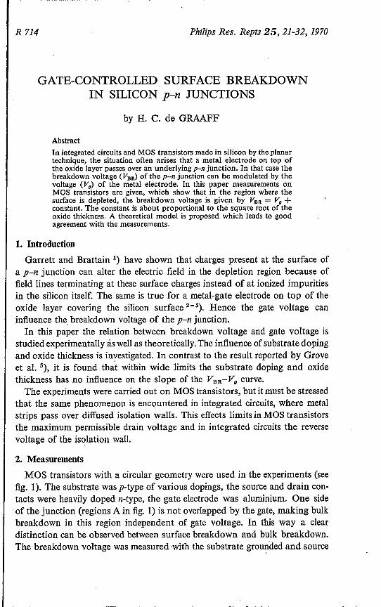
MOS transistors with a circular geometry were used in the experiments (seefig. I). The substrate was p-type of various dopings, the source and drain con-tacts were heavily doped n-type, the gate electrode was aluminium. One sideof the junction (regions A in fig. 1) is not overlapped by the gate, making bulkbreakdown in this region independent of gate voltage. In this way a cleardistinction can be observed between surface breakdown and bulk breakdown.The breakdown voltage was measured 'With the substrate grounded and source
22 H. C. de GRAAFF
. ~ +VSR
p
Fig. 1. Cross-section of the circular geometry of the MOS transistor. A is the junction region,not covered by the metal gate electrode, B is the covered region.
and drain interconnected, and at a constant current. Because all transistorsused in the experiments showed very sharp breakdown characteristics, thevalue of the constant breakdown current is of little importance. Itwas usually10 !LA.The source-drain distance was 17 (lm except in one case, where 400 (lm
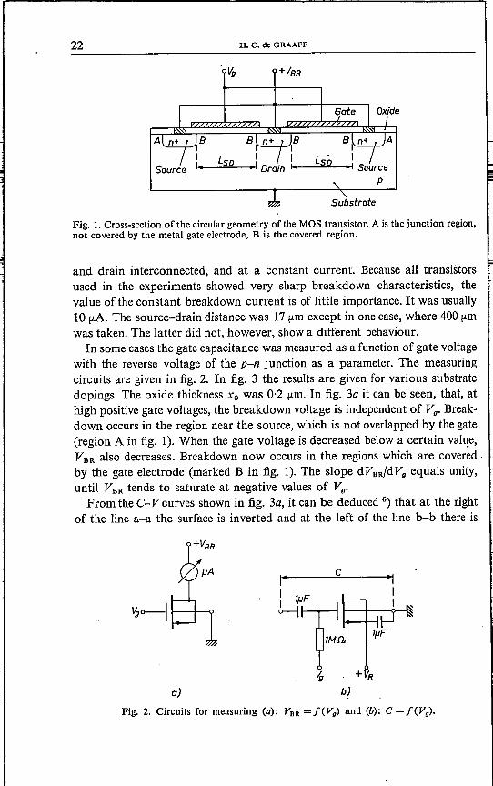
was taken. The latter did not, however, show a different behaviour.In some cases the gate capacitance was measured as a function of gate voltage
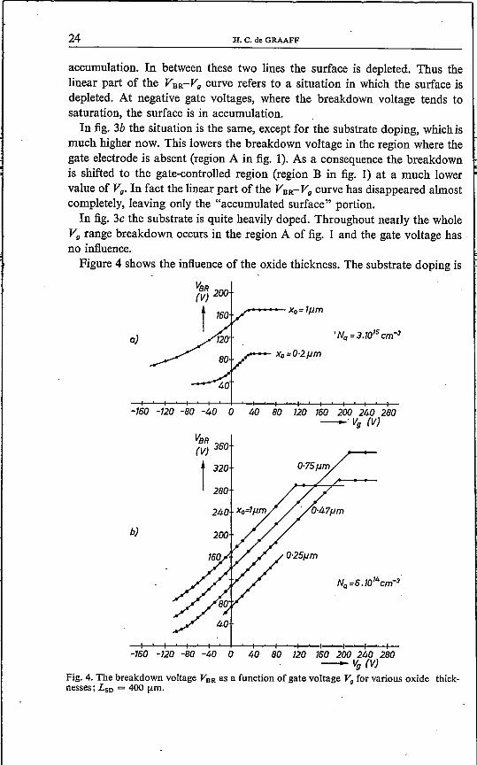
with the reverse voltage of the p-n junction as a parameter. The measuringcircuits are given in fig. 2. In fig. 3 the results are given for various substratedopings. The oxide thickness Xo was 0·2 (lm. In fig. 3a it can be seen, that, athigh positive gate voltages, the breakdown voltage is independent of Vg. Break-down occurs in the region near the source, which is not overlapped by the gate(region A in fig. I). When the gate voltage is decreased below a certain value,VBR also decreases. Breakdown now occurs in the regions which are coveredby the gate electrode (marked B in fig. I). The slope dVBR/dVg equals unity,until VBR tends to saturate at negative values of Vg.
From the C-V curves shown in fig. 3a, it can be deduced 6) that at the rightof the line a-a the surface is inverted and at the left of the line b-b there is
C
a)
Lr~~IM.a
~ . +VRb)
Fig. 2. Circuits for measuring (a): VBR=f(Vg) and (b): C=f(Vg).

GATE-CONTROLLED SURFACE BREAKDOWN IN SILICON pon JUNCTIONS 23
a)
/a/
//
/40 //
&-120 -80 -40 0 40 80 120 160 200
-~ (V)
VR=40V
b)
-80 -60 -40 -20 0
C(pF)
•I
20 40 60 80 100-Vg (V)
c) 8
vaR(V) 40
t bi 20
b a _----a-80 -60 -40 -20 0 20 40 60 80 100
-~ (V)
Fig. 3. The breakdown voltage VBR and the gate capacitance C as a function of the gatevoltage Vg for various substrate dopings Na. The oxide thickness Xo = 0·2 !Lm,the source-drain distance LSD = 17 !Lm.The lines a-a give the onset of inversion, the lines b-b the onsetof accumulation.
24 H. C. de GRAAFF
accumulation. In between these two lines the surface is depleted. Thus thelinear part of the VBR-Vg curve refers to a situation in which the surface isdepleted. At negative gate voltages, where the breakdown voltage tends tosaturation, the surface is in accumulation.In fig. 3b the situation is the same, except for the substrate doping, which is
much higher now. This lowers the breakdown voltage in the region where thegate electrode is absent (region A in fig. I). As a consequence the breakdownis shifted to the gate-controlled region (region B in fig. 1) at a much lowervalue of Vg. In fact the linear part of the VBR- Vg curve has disappeared almostcompletely, leaving only the "accumulated surface" portion.In fig. 3c the substrate is quite heavily doped. Throughout nearly the whole
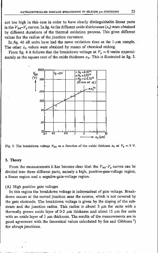
Vg range breakdown occurs in the region A of fig. land the gate voltage has .no influence.Figure 4 shows the influence of the oxide thickness. The substrate doping is
a)
_....-- xo=lJlm
-150 -120 -80 -40 0 40 80 120 150 200 240 280-'Vg (V)
b)
VSR(V) 350
1320
280
-150 -120 -80 -40 0 40 80 120 150 200 240 280-~(V)
Fig. 4. The breakdown voltage VDR as a function of gate voltage Vg for various oxide thick-nesses; LSD = 400 (Lm.
0·5 5 10---- Xo (pm)
2
GATE-CONTROLLED SURFACE BREAKDOWN IN SILICON pon JUNCTIONS 25
not too high in this case in order to have clearly distinguishable linear partsin the VBR-Vg curves. In fig.4a the different oxide thicknesses (xo) were obtainedby different durations of the thermal oxidation process. This gives differentvalues for the radius of the junction curvature.Infig. 4b all units have had the same oxidation time as the 1-(.Lm sample.
The other Xo values were obtained by means of chemical etching.From fig. 4 it follows that the breakdown voltage at Vg = 0 varies approxi-
mately as the square root of the oxide thickness xo. This is illustrated in fig. 5.
100
- +No =6.10't,.vg=ov_ IJ. No =3.10'5
o ND =4:5.10" I-(Grove et ol.)
vC1(Xl2~»)::y
»:~50
20
Fig. 5. The breakdown voltage VBR as a function of the oxide thickness Xo at Vg = 0 V.
3. Theory
From the measurements it has become clear that the VBR-V9 curves can bedivided into three different parts, namely a high, positive-gate-voltage region,a linear region and a negative-gate-voltage region.
(A) High positive gate voltagesIn this region the breakdown voltage is independent of gate voltage. Break-
down occurs at the curved junction near the source, which is not covered bythe gate electrode. The breakdown voltage is given by the doping of the sub-strate and the junction radius. This radius is about 3 (.Lmfor units with athermally grown oxide layer of 0·2 (.Lmthickness and about 12 (.Lmfor unitswith an oxide layer of 1 fLID thickness. The results of the measurements are ingood agreement with the theoretical values calculated by Sze and Gibbons 7)for abrupt junctions.

26 H. C. de GRAAFF
(B) The linear regionThe breakdown in this region occurs at the surface of the silicon substrate
and becomes apparent when the related breakdown voltage is lower than theone caused by the junction curvature.Normally the surface of p-type silicon would be inverted at positive gate
voltages. However, in the presence of a reversely biased p-n junction, the inver-sion disappears and the surface becomes depleted, as pointed out by Grove andFitzgerald 6). From the measured C-V curves it follows that in the whole linear I
region of the VBR-V9 curve the surface is depleted.In order to obtain more insight the following model was analyzed with the
aid of a computer. A two-dimensional plane diode is considered. The oxidelayer with thickness Xo is ~overed by a metal electrode (see fig. 6). The heavily
»:
-~:-I-_..,//~_JkIII I
I Iv=Vct v=vg v=o
x=wg
x-wy
n+ p
x=o x
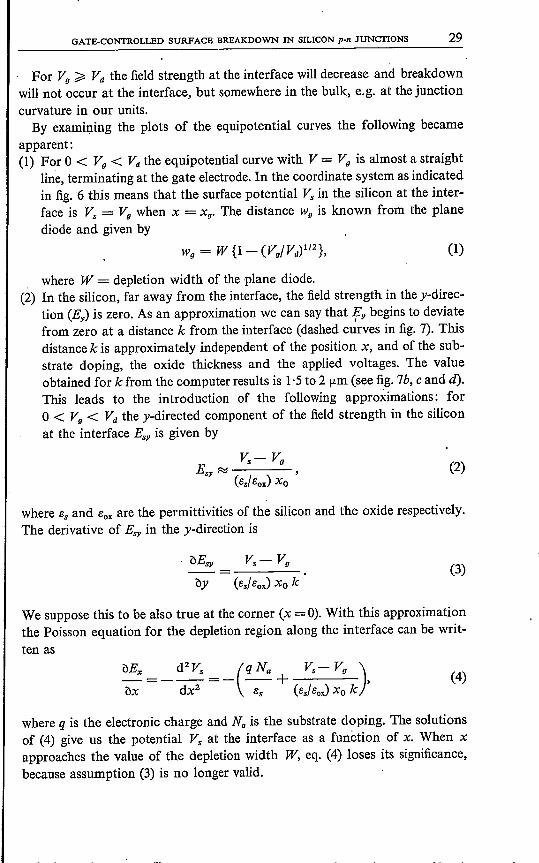
Fig. 6. The two-dimensional model: the metallurgical junction is situated at x = o.
doped tï" region is taken as an equipotential region with potential Vd' Thejunction is assumed to be abrupt. The potentialof the field-free region in thep-type substrate is taken as zero while the potentialof the metal electrode is Vg.For this structure the two-dimensional Poisson equation is solved numericallywith a digital computer using a relaxation method. As a first guess the voltagesof a plane junction are prescribed at the mesh points, except for the rightboundary. Here the voltages of a depleted surface are prescribed, taking thegate voltage Vg into account. The different relative dielectric constants of theoxide and the silicon (3·8 and 12 respectively) are taken into account by usinga modified difference equation for the interface. Surface-state charges and oxidecharge can be neglected in this case 8). This model is not suited for calculatingthe field strength in the corner of the n+ region at the interface, because theo-retically this field strength tends to infinity. In reality a thin depletion layer inthe n" region keeps the field strength everywhere finite. The model can be used,

GATE-CONTROLLED SURFACE BREAKDOWN IN SILICON pon JUNCTIONS 27
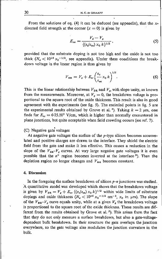
however, for calculating the equipotential curves. A few examples of suchcalculated equipotential curves are sketched in fig. 7. For Vg < Vd it can beseen that the equipotential curves bend to the left in the corner near the inter-face. This increases the field strength in this area; the highest field strengthwill be encountered at the point where the interface and the metallurgicaljunction intersect. Avalanche multiplication will start here and the multipliedcarriers are forced to move along the interface. The multiplication factor isdetermined by the integralof the ionization rate, taken along the interface.
ïutn,__,
a)
Vg=20V .xo =7·2jJm
~
l\' \ ,l 1k tIIII
Vd=70V 605040 30 20 70 0Na=1O'5cm-3
7E
b)
Fig. 7. Calculated equipotential curves for several drain and gate voltages and with variousoxide thicknesses. The substrate doping Na = 1015 cm- 3.

28 H. C. de GRAAFF .
c}
lil =OV ~xo=0·5pm,.\\, Ik \ t1 \ I \ i
I II I
II
l{j=50V 4.0 30 20 10 0No =10'5 ctrî?
turn,___.
~=20V . Vo=0'3pm
1\\\\, k 1" \1 'I
Vd=70V 505040 30 20 ID 0
Na = 10'5c.m~3
turn>--t
dj
Fig. 7 (continued).
The ionization rate itself is a function of the x-component (along the interface)of the field strength at the interface. Breakdown occurs when the multiplicationfactor goes to infinity. Instead of integrating the ionization rate, one can useas an approximation the 'critical-fleld concept. That means in this case thatbreakdown will occur when the x-directed component of the field strength atthe corner point (Esx(O)) reaches the critical value Eer.
GATE-CONTROLLED SURFACE BREAKDOWN IN SILICON p-n JUNCITONS 29
For Vg ~ Vd the field strength at the interface will decrease and breakdownwill not occur at the interface, but somewhere in the bulk, e.g. at the junctioncurvature in our units.By examining the plots of the equipotential curves the following became
apparent:(1) For 0 < Vg < Vd the equipotential curve with V = Vg is almost a straight
line, terminating at the gate electrode. In the coordinate system as indicatedin fig. 6 this means that the surface potential Vs in the silicon at the inter-face is Vs = Vg when x = Xg. The distance Wg is known from the planediode and given by
(1)
where W = depletion width of the plane diode.(2) In the silicon, far away from the interface, the field strength in the j-direc-
tion (E)I) is zero. As an approximation we can say that E)Ibegins to deviate,from zero at a distance k from the interface (dashed curves in fig. 7). Thisdistance k is approximately independent of the position x, and of the sub-strate doping, the oxide thickness and the applied voltages. The valueobtained for k from the computer results is 1·5to 2 (.Lm(see fig. 7b,c and d).This leads to the introduetion of the following approximations: foro < Vg < Vd the y-directed component of the field strength in the siliconat the interface Es)' is given by
(2)
where Es and Eox are the permittivities of the silicon and the oxide respectively.The derivative of Es)' in the y-direction is
(3)
We suppose this to be also true at the corner (x =0).With this approximationthe Poisson equation for the depletion region along the interface can be writ-ten as
(4)
where q is the electronic charge and Na is the substrate doping. The solutionsof (4) give us the potential Vs at the interface as a function of x. When xapproaches the value of the depletion width W, eq. (4) loses its significance,because assumption (3) is no longer valid.
Vd-VE = 9
xc {( / k}1/2 'e, Box) Xo(5)
30 H. C. de GRAAFF
From the solutions of eq. (4) it can be deduced (see appendix), that the x-directed field strength at the corner (x = 0) is given by
provided that the substrate doping is not too high and the oxide is not toothick (Na < 1016 Xo -1/2, see appendix). Under these conditions the break-down voltage in the linear region is thus given by
(B )1/2
VBR = Vg+ Eer "':""xo k .Box
(6)
This is the linear relationship between VBR and Vg,with slope unity, as knownfrom the measurements. Moreover, at Vg = 0, the breakdown voltage is pro-portional to the square root of the oxide thickness. This result is also in goodagreement with the experiments (see fig. 5). The encircled points in fig. 5 arethe experimental results obtained by Grove et al. 5). Taking k = 2 (Lm, onefinds for Eer = 6,25.105 V/cm, which is higher than normally encountered inplane junctions, but quite acceptable when field crowding occurs (see ref. 7).
•(C) Negative gate voltagesAt negative gate voltages the surface of the p-type silicon becomes accumu-
lated and positive charges are drawn to the interface. They shield the electric I
field from the gate and make it less effective. This causes a reduction in theslope of the VBR-V9 curves. At very large negative gate voltages it is evenpossible that the n+ region becomes inverted at the interface 9). Then thedepletion region no longer changes and VBR becomes constant.
4. Discussion
In the foregoing the surface breakdown of silicon p-n junctions was studied.A quantitative model was developed which shows that the breakdown voltageis given by VBR = Vg+ Eer {(Bs/Box) Xo k p/2 within wide limits of siibstratedopings and oxide thickness (Na < 1016 XO-1/2 cnr ", Xo in (Lm).The slopeof the VBR-Vg curve equals unity, while at a given Vg the breakdown voltageis proportional to the square root of the oxide thickness. These results are dif-ferent from the results obtained by Grove et al. 5). This arises from the factthat they do not only measure a surface breakdown, but also a gate-voltage-dependent bulk breakdown. In their structure the gate overlaps the junctioneverywhere, so the gate voltage also modulates the junction curvature in thebulk.
GATE-CONTROLLED SURFACE BREAKDOWN IN SILICON p-II JUNCTIONS 31
AcknowledgementThe author wishes to express his gratitude to Mr R. J. M. Verbeek, who
took a very active part in programming the computer.
Appendix
The differential equation (4) must be solved with the following boundaryconditions:
Vs = Vd at x = 0and
This leads toqNa
Vs = Vg + A exp (xXo -1/2) + B exp (-x XO-1/2) -Xo _-,Bs
with Xo = (es/Box) Xo k and A and B given by the boundary conditions. Thex component of the field strength at the interface is given by
dV.Esx = - - = _XO-1/2 {A exp (XXO-1/2) - B exp (_XXO-1/2)}.dx
At the corner (x = 0) we find:
Esx(O) = Exc = (B - A) Xo -1/2.
Inserting the values for A and B gives
In all cases encountered in our experiments Wg ~ 2Xol/2, so coth (wgXo -1/2)= 1. This reduces Exc to
If the second term between the brackets can be neglected in comparison to thefirst, the equation simplifies to
Eindhoven, Apri/1968
32 H. C. de GRAAFF
Omitting this second term is allowed when
or when1·76
N ~ -- . 1016 cm-3A 1/2Xo
(Xo is the oxide thickness in microns).In our experiments wg ~2Xol/2 for all cases. When wg < 2XOl/2 under some
circumstances, coth (wg Xo -1/2) becomes dependent on Vg and the slope ofthe VBR-Vg curve will be less than unity.
REFERENCES1) C. G. B. Garrett and W. H. Brattain, J. appl. Phys. 27, 299-306, 1956.2) W. Shockley and W. W. Hooper, The surface controlled avalanche transistor, Paper
presented at the Wescon Meeting, Los Angeles, 1964.3) S. R. Hofstein and F. B. Heiman, Proc. IEEE 51, 1190-1202, 1963.4) P. P. Castrucci and J. S. Logan, IBM J. Res. Dev. 8, 394-399, 1964.5) A. S. Grove, O. Leistiko and W. W. Hooper, IEEE Trans. El. Dev. ED-14, 157-162,
1967.6) A. S. Grove and D. J. Fitzgerald, Solid State Electron. 9, 783-806, 1966.7) S. M. Sze and G. Gibbons, Solid State Electron. 9,831-845, 1966.8) H. C. de G raaff and J. A. van Nielen, Electr. Letters 3, 195-196,1967.9) A. S. Grove and D. J. Fitzgerald, IEEE Trans. El. Dev. ED-12, 619-626, 1965.