general atomics phy proposal to...
TRANSCRIPT

January 2005 doc.: IEEE 802.15-05-0016-01-004a
Submission Naiel Askar- General AtomicsSlide 1
Project: IEEE P802.15 Working Group for Wireless Personal Area Networks (WPANS)
Submission Title: [General Atomics Call For Proposals Presentation]
Date Submitted: [4 January 2005]Source: Naiel Askar, Susan Lin, General Atomics- Photonics Division, Advanced Wireless Group, 10240 Flanders Ct, San Diego, CA 92121-2901, Voice +1 (858) 457-8700], Fax [+1 (858) 457-8740], E-mail [[email protected]}
Re: [802.15.4a Call For Proposal]
Abstract: [This presentation outlines General Atomics’ PHY proposal to the IEEE 802.15.4a Task Group]
Purpose: [To communicate a proposal for consideration by the standards committee]
Notice: This document has been prepared to assist the IEEE P802.15. It is offered as a basis for discussion and is not binding on the contributing individual or organization. The material in this document is subject to change in form and content after further study. The contributor reserves the right to add, amend or withdraw material contained herein.
Release: The contributor acknowledges and accepts that this contribution becomes the property of IEEE and may be made publicly available by P802.15.

January 2005 doc.: IEEE 802.15-05-0016-01-004a
Submission Naiel Askar- General AtomicsSlide 2
Overview of General AtomicsPHY Proposal to IEEE 802.15.4a
Naiel Askar, PhDSusan Lin, PhD
www.ga.com/uwb

January 2005 doc.: IEEE 802.15-05-0016-01-004a
Submission Naiel Askar- General AtomicsSlide 3
Outline of Presentation• Summary of proposal• Parameters and band plan• Proposal details• Ranging approach• Evaluation based on selection criteria
January 2005 doc.: IEEE 802.15-05-0016-01-004a
Submission Naiel Askar- General AtomicsSlide 4
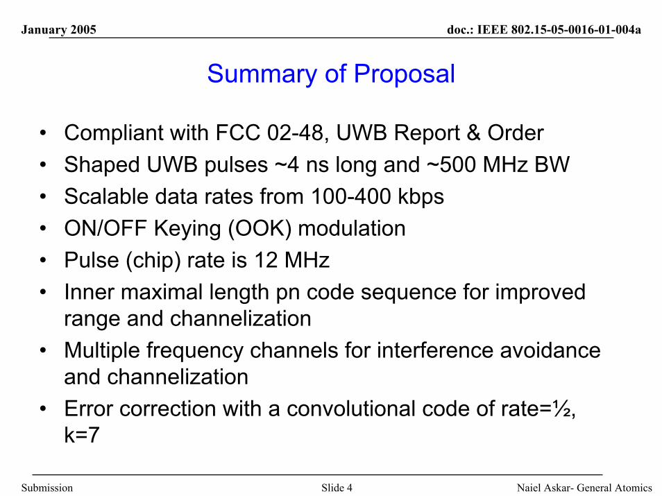
Summary of Proposal
• Compliant with FCC 02-48, UWB Report & Order• Shaped UWB pulses ~4 ns long and ~500 MHz BW• Scalable data rates from 100-400 kbps• ON/OFF Keying (OOK) modulation• Pulse (chip) rate is 12 MHz• Inner maximal length pn code sequence for improved
range and channelization• Multiple frequency channels for interference avoidance
and channelization• Error correction with a convolutional code of rate=½,
k=7

January 2005 doc.: IEEE 802.15-05-0016-01-004a
Submission Naiel Askar- General AtomicsSlide 5
Features
• Spectral flexibility to avoid interference and satisfy different international regulations
• Simple architecture facilitates one chip CMOS or SiGe solution
• Long guard period between pulses enhances multipath immunity
• Ultra low power consumption through simple architecture and low duty cycle
• Scalable receiver architectures that can provide tradeoff between complexity and performance

January 2005 doc.: IEEE 802.15-05-0016-01-004a
Submission Naiel Askar- General AtomicsSlide 6
Major System Parameters
100, 200 kbpsData rates supported with repeat codes
M-sequence length 15Spreading codeOn-Off keyingModulation
800 kbpsBit rate after coding
1Symbols per pulse
400 kbpsData rate before codingR=1/2, k=7Convolutional code
12 MHzPulse rate3No of Frequency Channels3.30 – 4.82 GHzUtilized SpectrumValueParameter

January 2005 doc.: IEEE 802.15-05-0016-01-004a
Submission Naiel Askar- General AtomicsSlide 7
Band Plan
3 3.5 4 4.5 5-20
-18
-16
-14
-12
-10
-8
-6
-4
-2
0
Frequency (GHz)
Am
plitu
de (d
B)
• 3 orthogonal frequency channels in the 3.1-5.0 GHz band
• Provides flexibility for worldwide spectrum regulations
• Channel scan may be used to avoid interference
• Each may have its own orthogonal pn code
ChannelCenter Frequency
(GHz)Upper Frequency
(GHz)Lower Frequency
(GHz)1 3.48 3.74 3.222 4.02 4.28 3.763 4.56 4.82 4.30

January 2005 doc.: IEEE 802.15-05-0016-01-004a
Submission Naiel Askar- General AtomicsSlide 8
Spectral Flexibility is Essential for Outdoors Operation
• Outdoor spectrum surveys in USA for the 3.1-5 GHz band show high levels of interference – It is expected that worldwide surveys will show similar results
• Outdoors UWB system will need to be able to select usable band based on spectral surveys

January 2005 doc.: IEEE 802.15-05-0016-01-004a
Submission Naiel Askar- General AtomicsSlide 9
Transmit Pulse Shaping• Triangular or half cosine short pulses ~ 4 ns
– Polarity of pulses scrambled to flatten spectrum• Pulses repeated at 12 MHz rate
– Minimal multipath interference between pulses• Immune from distortion or ringing from antennas or filters owing to relatively
long pulse time
3 3.5 4 4.5 5-20
-18
-16
-14
-12
-10
-8
-6
-4
-2
0
Frequency (GHz)
Am
plitu
de (d
B)
0 1 2 3 4 5 6-1
-0.8
-0.6
-0.4
-0.2
0
0.2
0.4
0.6
0.8
1
Time(ns)
Am
plitu
de

January 2005 doc.: IEEE 802.15-05-0016-01-004a
Submission Naiel Askar- General AtomicsSlide 10
OOK Modulation Enables Simple Transmitter Architecture• OOK requires a very simple transmitter architecture• Pulses with different center frequencies may be generated without
a local oscillator• Separation of pulses by ~83 ns provides enough time for multipath
decay
~4 ns
Symbol period = ~83.3 ns
Time
Logic 0no pulse sent
Logic 1Logic 1 Logic 1
Convolutionalencoder
pn codespreading Pulse generator
Polarity Band select
Data

January 2005 doc.: IEEE 802.15-05-0016-01-004a
Submission Naiel Askar- General AtomicsSlide 11
Spreading Code Description
• Spreading code increases SNR per bit and provides isolation for multiple uncoordinated piconets
• Maximal length (m-sequence) with m=4, n=15 will be utilized– Logic 1 uses the sequence Logic 0 is the inverse
• Each channel will have its own orthogonal sequence• Additional repeat code can tradeoff range for lower data
rates
010110010001111Seq. 3101011001000111Seq. 2001000111101011Seq. 1

January 2005 doc.: IEEE 802.15-05-0016-01-004a
Submission Naiel Askar- General AtomicsSlide 12
Simultaneously Operating Piconets
• Three nearly orthogonal frequency channels have been identified– orthogonal spreading code will increase isolation between
piconets– Shaped pulses will reduce spillage from one channel to next
• More channels can be defined with orthogonal spreading codes
January 2005 doc.: IEEE 802.15-05-0016-01-004a
Submission Naiel Askar- General AtomicsSlide 13
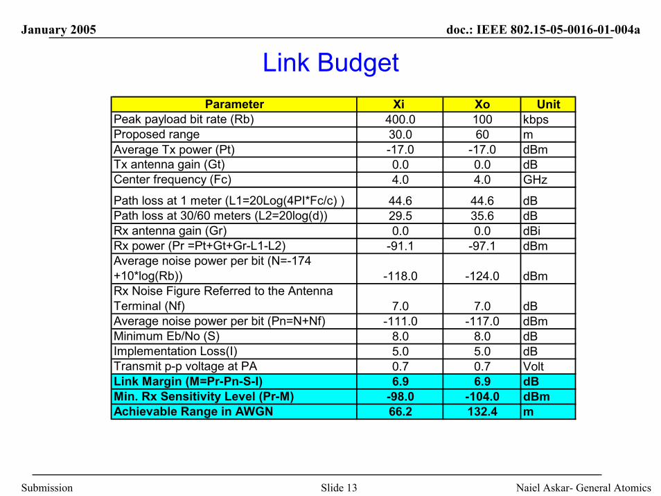
Link BudgetParameter Xi Xo Unit
Peak payload bit rate (Rb) 400.0 100 kbpsProposed range 30.0 60 mAverage Tx power (Pt) -17.0 -17.0 dBmTx antenna gain (Gt) 0.0 0.0 dBCenter frequency (Fc) 4.0 4.0 GHz
Path loss at 1 meter (L1=20Log(4PI*Fc/c) ) 44.6 44.6 dBPath loss at 30/60 meters (L2=20log(d)) 29.5 35.6 dBRx antenna gain (Gr) 0.0 0.0 dBiRx power (Pr =Pt+Gt+Gr-L1-L2) -91.1 -97.1 dBmAverage noise power per bit (N=-174 +10*log(Rb)) -118.0 -124.0 dBmRx Noise Figure Referred to the Antenna Terminal (Nf) 7.0 7.0 dBAverage noise power per bit (Pn=N+Nf) -111.0 -117.0 dBmMinimum Eb/No (S) 8.0 8.0 dBImplementation Loss(I) 5.0 5.0 dBTransmit p-p voltage at PA 0.7 0.7 VoltLink Margin (M=Pr-Pn-S-I) 6.9 6.9 dBMin. Rx Sensitivity Level (Pr-M) -98.0 -104.0 dBmAchievable Range in AWGN 66.2 132.4 m
January 2005 doc.: IEEE 802.15-05-0016-01-004a
Submission Naiel Askar- General AtomicsSlide 14
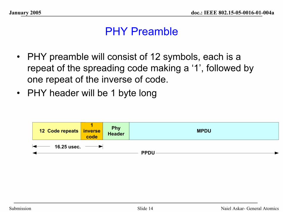
PHY Preamble
• PHY preamble will consist of 12 symbols, each is a repeat of the spreading code making a ‘1’, followed by one repeat of the inverse of code.
• PHY header will be 1 byte long
12 Code repeats1
inversecode
PhyHeader MPDU
PPDU16.25 usec.

January 2005 doc.: IEEE 802.15-05-0016-01-004a
Submission Naiel Askar- General AtomicsSlide 15
Time-Difference-of-Arrival (TDOA) Location Algorithm using One-Way Ranging (OWR)
• TDOA determines relative position of the mobile transmitter withrespect to the anchor receiver– No clock accuracy requirement for mobile– Need synchronization between anchor receivers
• Ranging function may be carried out in multiple frequency channels – Increases resolution accuracy
• Three TDOA measurements are needed for target location estimation

January 2005 doc.: IEEE 802.15-05-0016-01-004a
Submission Naiel Askar- General AtomicsSlide 16
TDOA Measurements & Location Estimation
Mobile TX
Anchor 1 RX
Anchor 2 RX
Anchor 3 RX
Isoc
hron
ous
T1
T2
T3
),( mm yxMobile
Anchor 2),( 22 AA yx
Anchor 3),( 33 AA yx
Anchor 1),( 11 AA yx
21
21
22
2212 )()()()()( mAmAmAmA yyxxyyxxTTc −+−−−+−=−
23
23
22
2232 )()()()()( mAmAmAmA yyxxyyxxTTc −+−−−+−=−

January 2005 doc.: IEEE 802.15-05-0016-01-004a
Submission Naiel Askar- General AtomicsSlide 17
Manufacturability & Technical Feasibility
• One chip solution in CMOS or SiGe– Chips based on this technology are available
• The relatively long subpulse time makes it immune from distortion or ringing from antennas or filters owing to Relaxed antenna characteristics
• A simple analog based solution or a digital high performance receiver are both feasible

January 2005 doc.: IEEE 802.15-05-0016-01-004a
Submission Naiel Askar- General AtomicsSlide 18
Scalable Receiver Architectures
• Receiver architecture scalable from a simple analog solution to a Rake based digital solution
Amplifier
Square LawDetector
BP Filter CodeDespread
Viterbidecoder
Digital Receiver
Switchable BP filters ThresholdDetector
MultibandOscillator
Amplifier ADC
ADC
0 90
Mixer
LP Filter
LP Filter
BP Filter RakeCombiner
CodeDespread
Viterbidecoder
Digital Receiver

January 2005 doc.: IEEE 802.15-05-0016-01-004a
Submission Naiel Askar- General AtomicsSlide 19
Conclusions
• UWB pulsed multiband system• Multiple frequency channels provide spectral flexibility
and robustness against interference. • Low signal repetition frequency to reduce inter chip
interference and reduce power consumption• Scalable architecture for lower cost and power and
higher performance• Remaining material will be presented at the next
opportunity• General Atomics will actively pursue opportunities for
merging with other proposals