gns7560 ste nowatermark - futureelectronics.com 1. general description the gns7560 is a...
TRANSCRIPT

CONFIDENTIA
L
1. General description
The GNS7560 is a high-performance single-chip L1 GPS solution for cellular handset applications.The advanced GPS baseband is the result of more than 20 years investment in GPS technology and 10 generations of products. The solution offers best-in-class acquisition and tracking sensitivity, Time-To-First-Fix (TTFF) and accuracy.The device minimizes system power consumption with ultra-low energy-per-fix due to the ultra-low power consumption and a set of power management modes designed into the GPS RF and baseband architecture.The GNS7560 supports both fully-autonomous operation for use in handheld consumer navigation devices and other standalone navigation systems, and Assisted-GPS (A-GPS) operation on GSM, WCDMA and CDMA networks.The GNS7560-hosted architecture shifts the non-real-time-critical navigation software to the host system’s microprocessor, minimizing system cost and PCB size. Host software drivers are available for the most popular operating systems for handsets and other portable devices.The highly integrated solution allows easy integration by providing connections for RF, clock inputs, host serial interface, and power.The GNS7560 is supported with full reference designs, demonstration systems, software development kits and other documentation.
2. Features
Best-in-class acquisition and tracking sensitivity, TTFF and accuracy
158 dBm acquisition-assisted, 160 dBm track using internal LNAs
Optimized for cellular handsets
Advanced proprietary multipath algorithms for robust low-dropout tracking in indoor and very low signal environments
Hosted architecture optimized for cost and performance
Supports GSM, WCDMA and CDMA control plane A-GPS assistance data standards
Supports SUPL user plane A-GPS assistance data
Exceeds 3GPP and TIA performance requirements
Ultra-low power consumption: < 18mW in tracking mode
Supports all cellular handset reference frequencies
WLCSP: 54 ball, 2.44 mm 3.64 mm 0.57 mm
TFBGA option: 54 ball, for low-cost manufacturing environments
Ultra-low external component count to enable a PCB footprint of less than 25 mm2
2 UARTs and SSI host interfaces
Temperature range 40 C to +85C
GNS7560High-performance single-chip A-GPS solutionRev. 2.2 — 7 May 2010 Final Datasheet
CONFIDENTIA
L
GNS7560R20 © ST-ERICSSON 2013. All rights reserved.
Final Datasheet Rev. 2.2 — 7 May 2010 2 of 35
GNS7560High-performance single-chip A-GPS solution
3. Applications
Cellular handset integration for navigation and location-based services
Handheld consumer navigation and multifunction devices
Battery-operated GPS devices
4. Ordering information
[1] Minimum order quantity: 5000 units for GNS7560ET2UM and 2000 units for GNS7560UK214TS.
5. Block diagram
Table 1. Ordering information[1]
Type number Package
Name Description Version
GNS7560UK214TS WLCSP54 wafer level chip-size package; 54 bumps; 2.44 3.64 0.57 mm GNS7560UK/N2
GNS7560ET2GE TFBGA54 plastic thin fine-pitch ball grid array package; 54 balls (7560/N2 is marked on IC) - Tray SOT1065-1
GNS7560ET2UM TFBGA54 plastic thin fine-pitch ball grid array package; 54 balls (7560/N2 is marked on IC) - Tape&Reel 13”
SOT1065-1
GNS7560ET2GA TFBGA54 plastic thin fine-pitch ball grid array package; 54 balls (7560/N2 is marked on IC) - Single Tray
SOT1065-1
GNS7560ET2HFUM TFBGA54 plastic thin fine-pitch ball grid array package; 54 balls (7560/N2 is marked on IC) - Halogen Free version
SOT1065-1
(1) Consult Applications team for correct information on front end configurations.
(2) NMEA 0183 stream converter.
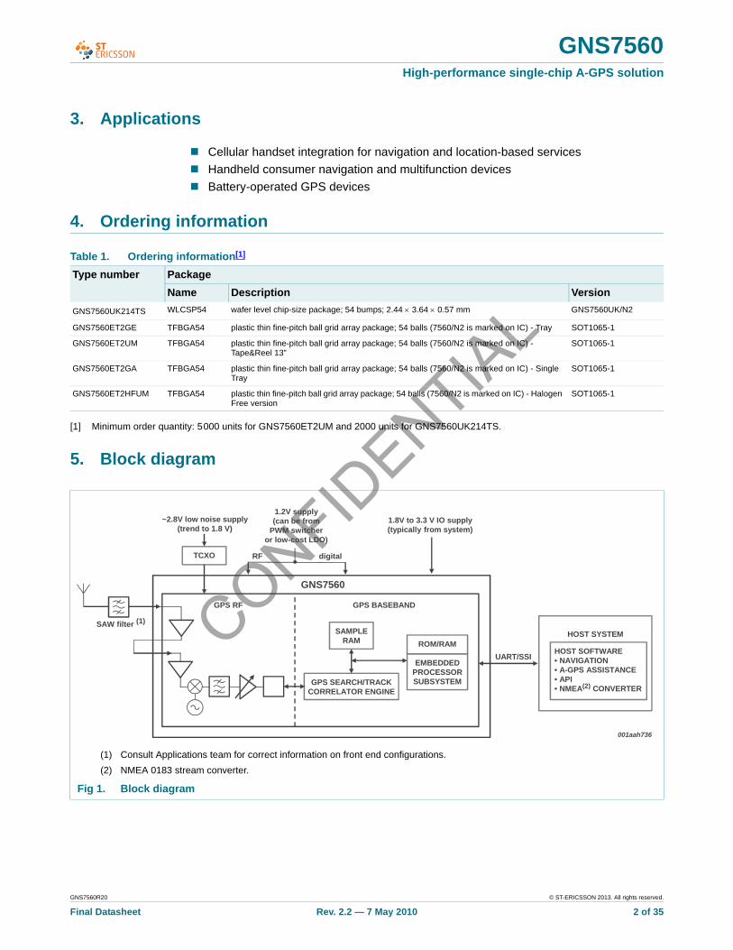
Fig 1. Block diagram
HOST SYSTEM
GNS7560
GPS RF GPS BASEBAND
SAMPLERAM
GPS SEARCH/TRACKCORRELATOR ENGINE
ROM/RAM
TCXO
~2.8V low noise supply(trend to 1.8 V)
1.2V supply(can be from
PWM switcheror low-cost LDO)
1.8V to 3.3 V IO supply(typically from system)
HOST SOFTWARE• NAVIGATION• A-GPS ASSISTANCE• API• NMEA(2) CONVERTER
UART/SSI
SAW filter (1)
RF digital
EMBEDDEDPROCESSORSUBSYSTEM
001aah736
CONFIDENTIA
L
GNS7560R20 © ST-ERICSSON 2013. All rights reserved.
Final Datasheet Rev. 2.2 — 7 May 2010 3 of 35
GNS7560High-performance single-chip A-GPS solution
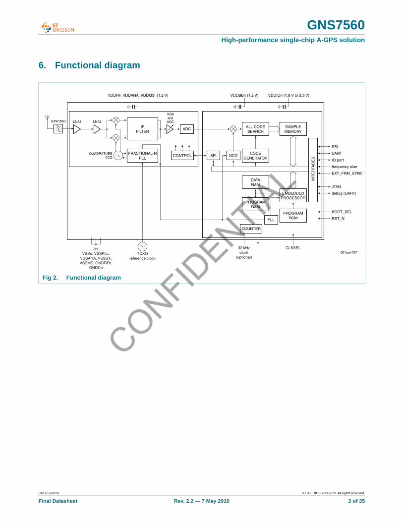
6. Functional diagram
Fig 2. Functional diagram
001aah737
LNA1
IFFILTER
FRACTIONAL-NPLL
LNA2
QUADRATUREVCO
SAW filter
VGAandAGC
ADC
PLL
CONTROL
SSI
UART
IO port
JTAG
debug (UART)
frequency plan
EXT_FRM_SYNC
BOOT_SEL
RST_N
VDDRF, VDDANA, VDDMS (1.2 V) VDDBBn (1.2 V) VDDIOn (1.8 V to 3.3 V)
INT
ER
FAC
ES
SPI NCO
COUNTER
CODEGENERATOR
ALL CODESEARCH
SAMPLEMEMORY
DATARAM
PROGRAMRAM
EMBEDDEDPROCESSOR
PROGRAMROM
VSSn, VSSPLL,VSSANA, VSSSX,VSSMS, GNDRFn,
GNDCn
TCXOreference clock
32 kHzclock
(optional)
CLKSEL

CONFIDENTIA
L
GNS7560R20 © ST-ERICSSON 2013. All rights reserved.
Final Datasheet Rev. 2.2 — 7 May 2010 4 of 35
GNS7560High-performance single-chip A-GPS solution
7. Pinning information
7.1 Pinning
Fig 3. Pin configuration; ball position (view from top)
001aah755
GNS7560UKN214TS
Transparent top view
J
H
G
F
D
B
E
C
A
2 4 61 3 5
bump A1
index area
Table 2. Pin allocation table
Pin Symbol Pin Symbol Pin Symbol
A1 MODE1 D1 VDDIO2 G1 GNDRF1
A2 VSS3 D2 UART2_RXD/SSI_SLV_CLKIN G2 VDDRF
A3 VDDBB2 D3 DEBUG_BOOT G3 TESTOUT
A4 VSS2 D4 PULSE_OUT G4 GNDC1
A5 VDDIO1 D5 PWM_OUT G5 GNDC2
A6 VSSPLL D6 RST_N G6 VSSMS
B1 VSS4 E1 GPIO[12] H1 RFINP
B2 MODE0 E2 EXT_FRM_SYNC H2 GNDRF2
B3 MODE3 E3 UART2_TXD/SSI_SLV_SO H3 VDDANA
B4 GPIO[3] E4 LNA_EN H4 TESTIN
B5 UART2_CTS/SSI_SLV_CS E5 VDDBB1 H5 SXTEST
B6 TCXO_EN E6 VSS1 H6 VDDMS
C1 VDDBB3 F1 BOOT_SEL0 J1 RFINM
C2 CLKSEL F2 BOOT_SEL1 J2 SAWIN
C3 MODE2 F3 BOOT_SEL2 J3 SAWOUT/RFIN2
C4 EXT_DUTY_CYCLE F4 UART1_TXD J4 VSSANA
C5 UART2_RTS/SSI_SLV_SI F5 CLK32KIN J5 VSSSX
C6 UART1_RXD F6 CLK32KOUT J6 TCXO_IN

CONFIDENTIA
L
GNS7560R20 © ST-ERICSSON 2013. All rights reserved.
Final Datasheet Rev. 2.2 — 7 May 2010 5 of 35
GNS7560High-performance single-chip A-GPS solution
Table 3 shows the pinout of the GNS7560 device, detailing the BGA number, the pin name and a brief description of its function.
Table 3. Pin description
Symbol Pin Type[1] Description
Power supplies
VDDBB1 E5 P 1.2 V power supply for baseband core
VDDBB2 A3
VDDBB3 C1
VDDIO1 A5 P 1.8 V or 2.5 V or 3.3 V power supply for I/O cells
VDDIO2 D1
VDDRF G2 P 1.2 V power supply for LNA section of RF
VDDANA H3 P 1.2 V power supply for IF analog section
VDDMS H6 P 1.2 V power supply for mixed signal section (ADC and programmable gain amplifier)
VSS1 E6 P ground for baseband
VSS2 A4
VSS3 A2
VSS4 B1
VSSPLL A6 P analog ground for internal PLL block
GNDRF1 G1 P ground for LNA1 section of RF
GNDRF2 H2 P ground for LNA2 section of RF
GNDC1 G4 P cold ground
GNDC2 G5
VSSANA J4 P ground for IF analog section
VSSSX J5 P ground for analog section which includes frequency synthesizer
VSSMS G6 P ground for mixed signal section (ADC and programmable gain amplifier)
RF input
RFINM J1 I LNA () RF input[2]
RFINP H1 I LNA (+) RF input[2]
SAWIN J2 O LNA1 output; in normal configuration this is connected to the input of the SAW filter
SAWOUT/RFIN2 J3 I LNA2 input or RF input;
in normal configuration this is connected to the output of the SAW filter
when the device is used with an external LNA this is the RF input
Clock interfaces
CLK32KIN F5 I 32 kHz clock input for on-chip counter
CLK32KOUT F6 O 32 kHz clock output

CONFIDENTIA
L
GNS7560R20 © ST-ERICSSON 2013. All rights reserved.
Final Datasheet Rev. 2.2 — 7 May 2010 6 of 35
GNS7560High-performance single-chip A-GPS solution
CLKSEL C2 I clock selection input;
LOW = internal PLL clock
HIGH = external 32 kHz clock
When CLKSEL is set to HIGH the device will boot in low power mode with the UART baud rate set to 600baud. The Host software will download the frequency of the TCXO crystal being used. When using this mode the BOOTSEL[0:2] inputs are set to {1,1,1}
TCXO_IN J6 I external TCXO GPS reference clock input
Boot mode selection
BOOT_SEL0 F1 I boot mode selection inputs 0 to 2; see Table 19
BOOT_SEL1 F2
BOOT_SEL2 F3
RST_N D6 I asynchronous reset, active LOW
I/O port interface[3]
GPIO[3] B4 I/O GPIO input or output: not used
output with 4 mA drive current
When using UART host interface this I/O should be left unconnected. When using SPI mode this pin should have a 1k Ohm pull down resistor.
EXT_FRM_SYNC E2 I external sync input to synchronize the GPS engine to an external source with sub 1 ms timing;
input with pull-down resistor
PULSE_OUT D4 I/O 1 pulse-per-second input; used for timing applications
output with 4 mA drive current
UART2_RXD/SSI_SLV_CLKIN D2 I UART2 receive data input (host interface) or SSI receive serial clock input
UART2_TXD/SSI_SLV_SO E3 O UART2 transmit data output (host interface) or SSI transmit serial data output to host (serial output);
output with 2 mA drive current
UART1_RXD C6 I UART1 receive data input (test interface);
input with pull-up resistor
EXT_DUTY_CYCLE C4 I/O external duty cycle control input;
GPIO input or output with 4 mA drive current and pull-down resistor
PWM_OUT D5 I/O input or output with 2 mA drive current
UART1_TXD F4 O UART1 transmit data output (test interface);
output with 2 mA drive current
LNA_EN E4 I/O external LNA enable output; see Table 7
input or output with 2 mA drive current and pull-down resistor
TCXO_EN B6 I/O external TCXO enable output; see Table 7
input or output with 4 mA drive current and pull-up resistor
Table 3. Pin description …continued
Symbol Pin Type[1] Description

CONFIDENTIA
L
GNS7560R20 © ST-ERICSSON 2013. All rights reserved.
Final Datasheet Rev. 2.2 — 7 May 2010 7 of 35
GNS7560High-performance single-chip A-GPS solution
[1] P = power supply, I = input, O = output, I/O = input/output.
[2] The device uses a differential front end to enable the lowest cost solution. If a single-ended antenna is used, a balun is used to match the input to the antenna.
[3] The I/O port interface pins can carry information for either the UARTs or the slave SSI depending on the setting of MODE[3:0] pins; see Table 21.
8. Functional description
8.1 System overview
The GNS7560 provides a complete GPS solution designed for ease of integration into host platforms. The key components are described below.
• Baseband channel block
– Flexible architecture readily adaptable to specific market, air interface and silicon cost requirements
• GPS software
– Indoor acquisition and tracking
– Network-assistance ready (mobile-based, mobile-assisted, CDMA, W-CDMA, GSM, control plane and user plane)
– Stand-alone GPS operation
– Support of different location-based service protocols
– Instant fixes
• Host-based navigation software (See also Section 8.6)
– Well-defined API for control and reporting to host applications
– ‘OS wrapper’ enabling simple porting to customer-preferred operating system
UART2_CTS/SSI_SLV_CS B5 I/O UART2 clear-to-send (host interface) or SSI to host chip select
input or output with 2 mA drive current, pull-up resistor and Schmitt trigger input
UART2_RTS/SSI_SLV_SI C5 I/O UART2 ready-to-send (host interface) or SSI to host serial input
input or output with 2 mA drive current and pull-up resistor
GPIO[12] E1 I/O GPIO input or output with 2 mA drive current: not used
Test and debug interfaces
TESTOUT G3 O IF test output
TESTIN H4 I test input
SXTEST H5 I/O test input or output (frequency synthesizer)
DEBUG_BOOT D3 I debug mode, trigger emulation boot, download monitor program
MODE0 B2 I host interface selection outputs for selecting either both UARTs or the slave SSI; see Table 21MODE1 A1
MODE2 C3
MODE3 B3
Table 3. Pin description …continued
Symbol Pin Type[1] Description

CONFIDENTIA
L
GNS7560R20 © ST-ERICSSON 2013. All rights reserved.
Final Datasheet Rev. 2.2 — 7 May 2010 8 of 35
GNS7560High-performance single-chip A-GPS solution
8.1.1 Receiver section
The GNS7560 includes a low-power, single-conversion low-IF GPS receiver for the 1.575 GHz, L1 signal. The device contains a fully-integrated GPS receive path, including LNAs, that down-convert the GPS L1 signal of 1575.42 MHz, to an IF signal quantized to 4 bits and delivered to the integrated GPS baseband device. The device also contains a fully-integrated frequency synthesizer that generates the correct LO frequency to down-convert the GPS signal starting from any reference frequency input, including all cellular handset reference frequencies.
8.2 GPS performance
The GNS7560 is a DSP-centric, highly-integrated design with reduced silicon, and cost-optimized for all current and next-generation air interfaces (CDMA, GSM/GPRS/EDGE, WCDMA/UMTS).
The baseband section has the following key features:
• Optimized for asynchronous networks
• Measurement engine with a search capacity of 42 channels
• Maximum acquisition sensitivity 158 dBm
The indoor and outdoor mixed-mode acquisition and tracking sensitivity performance characteristics are given in Table 4.
[1] CDMA aiding: time known to < 100 s, location known to < 3 km, oscillator known to 0.05 ppm, known ephemeris for available satellites (RMS).
[2] GSM (coarse) and WCDMA/3GPP aiding: time known to < 2 s, location known to < 3 km, oscillator known to 0.05 ppm, known ephemeris for available satellites (RMS).
8.2.1 Positional accuracy
Optimized for Location-Based Services (LBS) and better than FCC E911 mandate requirements and 3GPP 34.171 requirement; see Table 5.
Table 4. Acquisition and tracking performance
Acquisition/tracking mode LNA Signal level TTFF[1]
CDMA acquisition[1] 152 dBm 10 s
GSM/WCDMA/3GPP acquisition[2] internal 152 dBm <20 s
external 152 dBm <15 s
Hot start (open sky) 130 dBm 1 s
Cold start (open sky) 130 dBm <38 s
Lowest sensitivity: ephemeris decode (application-specific software-build dependent)
142 dBm to 145 dBm
Minimum tracking signal level (deep indoors) internal 160 dBm
external 160 dBm
Table 5. Positional accuracy
Accuracy (RMS value) Signal level
<5 m 135 dBm (outdoor)
<20 m 148 dBm (indoor)
<50 m 152 dBm (indoor)
CONFIDENTIA
L
GNS7560R20 © ST-ERICSSON 2013. All rights reserved.
Final Datasheet Rev. 2.2 — 7 May 2010 9 of 35
GNS7560High-performance single-chip A-GPS solution
8.2.2 Additional GPS-related features
• Channels: dynamic channel and dynamically configurable architecture management
• Positioning modes: autonomous/standalone, mobile-assisted, mobile-based, simultaneous or mixed modes, navigation (Kalman filter)
• Update rate: user selectable - event, position, command/request, periodic (2 per second to once per hour)
• Host software protocol support: NMEA 0183 STEricsson API air interface
• Application microprocessor requirements: no real-time processing requirements, only requirement is C-compiler and floating-point libraries
8.3 Additional features
• Embedded DSP
• UART and SSI host interfaces
• Configurable GPIO
• 1 pulse-per-second output (PULSE_OUT)
8.4 RF front end
The RF Front End (RFFE) includes two low-noise amplifiers with a fully-integrated 50 matching network on the second LNA, IF band-pass filter, VCO and high-performance fractional-N PLL.
8.5 GPS baseband
8.5.1 Overview
The GPS baseband provides the baseband signal processing for the GPS receiver (IF down-conversion, correlation and integration). The GPS baseband includes an embedded DSP whose firmware controls the baseband’s GPS acquisition and tracking. The DSP firmware is a ROM within the GNS7560, that does not require support from any external device. Higher-level software running on a separate host calculates navigation solutions (the host-based navigation software).
The GPS baseband has the following features:
• Embedded DSP
• Correlation engine
• GPS code generation
• Coherent and incoherent summation block
• Doppler wipe off
• Magnitude calculation
• Compare-and-threshold signal detection
• Timing and control
• Power saving
• Clocking architectures

CONFIDENTIA
L
GNS7560R20 © ST-ERICSSON 2013. All rights reserved.
Final Datasheet Rev. 2.2 — 7 May 2010 10 of 35
GNS7560High-performance single-chip A-GPS solution
• Two universal asynchronous receiver/transmitter interfaces:
– UART1: development tool for the embedded DSP firmware
– UART2: host interface to communicate with the host-based navigation software
• Slave Synchronous Serial Interface (SSI) for optional interface to an external host microprocessor
8.5.2 Embedded DSP firmware
The embedded DSP firmware performs the following functions:
• Interfaces to GPS baseband hardware
• Searches for satellites either autonomously or commanded using acquisition data from host
• When a satellite has been acquired, transitions to track the satellite
• Where possible, demodulates the satellite navigation message data
• During satellite tracking, monitors the signals for validity and multipath
• At the required update rate (typically 1 Hz) sends the latest raw satellite measurements to the host-based navigation software
All real-time, critical or high-interrupt rate functions are performed within the embedded DSP firmware.
8.5.3 Interface between GNS7560 and host-based navigation software
This interface is a two-way link, normally using a UART interface (UART 2), but can use the slave SSI interface. The max data rate that can be supported is 400kbps, however the physical layer can run at 3Mbps. The UART interface uses a 115.2 kBd data rate, transferring about 4 kB of data per update.
The host-based navigation software sends requests for when the next raw satellite measurements are required, and also provides satellite acquisition aiding data and channel/satellite reset commands.
The host-based navigation software also sends GNS7560 mode set commands for Sleep, Coma or Deep coma. The Sleep mode command also specifies a time-out for the automatic transition from Sleep to Coma mode. A wake-up command is also provided.
The GNS7560 responds by sending raw satellite measurements to the host-based navigation software at the requested time, and also provides the parity-checked raw subframes of the satellite navigation messages (when available).
8.6 Host-based navigation software
The host-based navigation software will run on a range of processors, notably ARM, and a variety of high-level and real-time operating systems. The purpose of this software is to provide the user application with GPS position information. To do this the GPS navigation software interfaces with the host microprocessor software, the operating system and the GNS7560.
The host-based navigation software performs the following functions:
• Interface to the GNS7560

CONFIDENTIA
L
GNS7560R20 © ST-ERICSSON 2013. All rights reserved.
Final Datasheet Rev. 2.2 — 7 May 2010 11 of 35
GNS7560High-performance single-chip A-GPS solution
• API interface to host software
• Satellite navigation message data decode and state table generation
• Satellite measurement generation (pseudorange, Doppler, etc.)
• Navigation Kalman filter task: calculates position, velocity, time, frequency
• Satellite pre-positioning: predicts where to search for a satellite
• Navigation output generation, including NMEA 0183 stream
The typical system requirements of the host software are:
• Memory requirement:
– ROM or flash 100 kB to 300 kB, OS dependent
– RAM - up to 100 kB - OS dependent
• Microprocessor requirement:
– Acquisition or tracking mode requires 5 MIPS (32-bit ARM MIPS) on the host microprocessor
• Basic OS functions required:
– Memory allocation/de-allocation
– Basic input/output
– System timers
– Thread management
• Floating-point libraries available for:
– IEEE 8-byte double precision
– IEEE 4-byte float single precision
Other system features which need to be considered are:
• Availability of optional external 32 kHz clock to OS
• Availability of NVRAM or file system to OS
• Type of serial interface to GNS7560
• Microprocessor type and clock speed
• Interface to location application, such as mapping:
– Virtual serial port
– Memory buffer
– NMEA messages required
8.7 Clocks
8.7.1 TCXO clock input
The GNS7560 can accept a variety of different GPS clock input frequencies. Sensitivity performance may vary depending on the reference frequency used at the TCXO input; in particular reference frequencies whose harmonics fall within about 1 MHz of the GPS RF signal center frequency (1575.42 MHz) band are more likely to cause performance degradation.
CONFIDENTIA
L
GNS7560R20 © ST-ERICSSON 2013. All rights reserved.
Final Datasheet Rev. 2.2 — 7 May 2010 12 of 35
GNS7560High-performance single-chip A-GPS solution
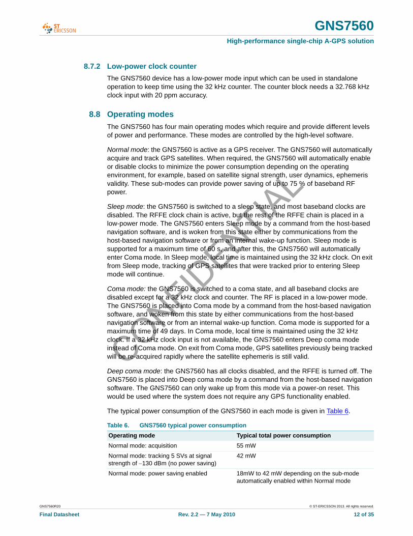
8.7.2 Low-power clock counter
The GNS7560 device has a low-power mode input which can be used in standalone operation to keep time using the 32 kHz counter. The counter block needs a 32.768 kHz clock input with 20 ppm accuracy.
8.8 Operating modes
The GNS7560 has four main operating modes which require and provide different levels of power and performance. These modes are controlled by the high-level software.
Normal mode: the GNS7560 is active as a GPS receiver. The GNS7560 will automatically acquire and track GPS satellites. When required, the GNS7560 will automatically enable or disable clocks to minimize the power consumption depending on the operating environment, for example, based on satellite signal strength, user dynamics, ephemeris validity. These sub-modes can provide power saving of up to 75 % of baseband RF power.
Sleep mode: the GNS7560 is switched to a sleep state, and most baseband clocks are disabled. The RFFE clock chain is active, but the rest of the RFFE chain is placed in a low-power mode. The GNS7560 enters Sleep mode by a command from the host-based navigation software, and is woken from this state either by communications from the host-based navigation software or from an internal wake-up function. Sleep mode is supported for a maximum time of 60 s, and after this, the GNS7560 will automatically enter Coma mode. In Sleep mode, local time is maintained using the 32 kHz clock. On exit from Sleep mode, tracking of GPS satellites that were tracked prior to entering Sleep mode will continue.
Coma mode: the GNS7560 is switched to a coma state, and all baseband clocks are disabled except for a 32 kHz clock and counter. The RF is placed in a low-power mode. The GNS7560 is placed into Coma mode by a command from the host-based navigation software, and woken from this state by either communications from the host-based navigation software or from an internal wake-up function. Coma mode is supported for a maximum time of 49 days. In Coma mode, local time is maintained using the 32 kHz clock. If a 32 kHz clock input is not available, the GNS7560 enters Deep coma mode instead of Coma mode. On exit from Coma mode, GPS satellites previously being tracked will be re-acquired rapidly where the satellite ephemeris is still valid.
Deep coma mode: the GNS7560 has all clocks disabled, and the RFFE is turned off. The GNS7560 is placed into Deep coma mode by a command from the host-based navigation software. The GNS7560 can only wake up from this mode via a power-on reset. This would be used where the system does not require any GPS functionality enabled.
The typical power consumption of the GNS7560 in each mode is given in Table 6.
Table 6. GNS7560 typical power consumption
Operating mode Typical total power consumption
Normal mode: acquisition 55 mW
Normal mode: tracking 5 SVs at signal strength of 130 dBm (no power saving)
42 mW
Normal mode: power saving enabled 18mW to 42 mW depending on the sub-mode automatically enabled within Normal mode
CONFIDENTIA
L
GNS7560R20 © ST-ERICSSON 2013. All rights reserved.
Final Datasheet Rev. 2.2 — 7 May 2010 13 of 35
GNS7560High-performance single-chip A-GPS solution
8.9 UART interfaces
The GNS7560 provides two identical, full-duplex, universal asynchronous receiver/transmitter interfaces:
• UART1 for development and test purposes
• UART2 for communication with the host-based navigation software
These interfaces are fully-compliant with the latest UART specifications and have a baud rate of 115200. The UARTs are based on the 16550 industry standard. If the UART host interface is required, then the GNS7560 UART2 should be connected to a dedicated UART port from the host, and not shared with any other functions.
It is not necessary that flow control be implemented (see detailed application notes)
9. Limiting values
10. Recommended operating conditions
Power supply sequencing. To avoid the possibility of latch-up it is highly recommended to turn on the higher supply voltage VDD(IO) first and then the lower supply voltage VDD(C)bb.
Sleep mode 15 mW
Coma mode 100 W
Deep coma mode 90 W
Table 7. External LNA enable (LNA_EN) and TCXO enable (TCXO_EN)
GNS7560 mode Pin LNA_EN External LNA state
Pin TCXO_EN TCXO state
Reset LOW Off HIGH On
Normal HIGH On HIGH On
Sleep LOW Off HIGH On
Coma and Deep Coma LOW Off LOW Off
Table 6. GNS7560 typical power consumption …continued
Operating mode Typical total power consumption
Table 8. Limiting valuesIn accordance with the Absolute Maximum Rating System (IEC 60134).
Symbol Parameter Conditions Min Max Unit
VDD(C)bb baseband core supply voltage
- 1.32 V
VDD(IO) I/O supply voltage - 3.6 V
VDD(C)RF RF core supply voltage - 1.32 V
Vn voltage on any other pin I/O pins - VDD(IO) + 0.2
V
Tstg storage temperature 55 +125 C
CONFIDENTIA
L
GNS7560R20 © ST-ERICSSON 2013. All rights reserved.
Final Datasheet Rev. 2.2 — 7 May 2010 14 of 35
GNS7560High-performance single-chip A-GPS solution
11. Characteristics
Table 9. Operating conditions
Symbol Parameter Conditions Min Typ Max
VDD(C)bb baseband core supply voltage
pins VDDBB1, VDDBB2, VDDBB3
1.08 1.2 1.32
VDD(IO) I/O supply voltage pins VDDIO1, VDDIO2 [1]
[1]The VDDIO supply can be between 1.8v and 3.3v however they are only characterized at 1.8v, 2.5v and 3.3v
[2]Must be supplied from low-noise LDO linear regulator. The maximum noise floor is 30V RMS
1.8 V supply 1.62 1.8 1.98
2.5 V supply 2.25 2.5 2.75
3.3 V supply 3.0 3.3 3.6
VDD(C)RF RF core supply voltage pins VDDRF, VDDANA, VDDMS
[2] 1.08 1.2 1.32
Vn voltage on any other pin I/O pins
1.8 V supply - 1.8 2.1
2.5 V supply - 2.5 2.8
3.3 V supply - 3.3 3.63
Tamb ambient temperature 40 +25 +85
Table 10. Power suppliesTamb = -40 C to +85 C unless otherwise specified.
Symbol Parameter Condition Min Typ Max Unit
Baseband core supply; pins VDDBB1, VDDBB2, VDDBB3 = 1.2 V 10%
IDD supply current Normal mode [1] - 23 40 mA
Sleep mode [2] - 2.4 - mA
Coma mode [3] 10 20 90 A
Deep coma mode [4] 10 20 90 A
ILI input leakage current VIN = VDD or GND - 2 - A
I/O supply
Pins VDDIO1, VDDIO2 = 3.3 V 10%
IDD supply current Normal mode [1] - 0.9 5 mA
Sleep mode [2] - 0.14 - mA
Coma mode [3] - 60 - A
Deep coma mode [4] - 60 - A
ILI input leakage current VIN = VDD or GND - 2 - A
Pins VDDIO1, VDDIO2 = 2.5 V 10%

CONFIDENTIA
L
GNS7560R20 © ST-ERICSSON 2013. All rights reserved.
Final Datasheet Rev. 2.2 — 7 May 2010 15 of 35
GNS7560High-performance single-chip A-GPS solution
[1] All systems active, running typical program.
[2] Embedded DSP static, PLL on and TCXO GPS reference clock running.
[3] 32 kHz oscillator running, all other I/O static. The TCXO will be off assuming the TCXO_EN is connected to the TCXO enable, current drain is mainly through the up resistor in the TCXO_EN I/O. Current also be higher depending on other I/O Connections.
[4] Deep coma mode is entered via a software command on the Host interface. When this command is received the device will power down the RF sections of the device and turn off the clocks. To exit this mode the RST_N is applied. Note however that on initial power up of the device and before RST_N is applied the power consumption can be as high as 20mA.
IDD supply current Normal mode [1] - 0.9 5 mA
Sleep mode [2] - 0.11 - mA
Coma mode [3] - 40 - A
Deep coma mode [4] - 40 - A
ILI input leakage current VIN = VDD or GND - 2 - A
Pins VDDIO1, VDDIO2 = 1.8 V 10%
IDD supply current Normal mode [1] - 0.11 5 mA
Sleep mode [2] - 0.11 - mA
Coma mode [3] - 30 - A
Deep coma mode [4] - 30 - A
ILI input leakage current VIN = VDD or GND - 2 - A
RF core supply; pins VDDRF, VDDANA, VDDMS = 1.2 V 10%
IDD supply current Normal mode [1] - 20 30 mA
Sleep mode [2] - 10.3 - mA
Coma mode [3] - 20 - A
Deep coma mode [4] - 20 - A
ILI input leakage current VIN = VDD or GND - 2 - A
Table 10. Power supplies …continuedTamb = -40 C to +85 C unless otherwise specified.
Symbol Parameter Condition Min Typ Max Unit
Table 11. Digital input/output characteristics
Symbol Parameter Conditions Min Typ Max Unit
3.3 V supply
VIL LOW-level input voltage 0.3 - +0.8 V
VIH HIGH-level input voltage 2.0 - 3.63 V
Vth threshold voltage all I/O pins 1.33 1.44 1.52 V
Vth(LH) LOW to HIGH threshold voltage 1.54 1.64 1.71 V
Vth(HL) HIGH to LOW threshold voltage 1.08 1.18 1.25 V
ILI input leakage current Vi = 3.0 V or 0 V - - 10 A
IOZ OFF-state output current VO = 3.0 V or 0 V - - 10 A
Ci input capacitance - 1.54 - pF
Rpu pull-up resistance 30 43 65 k
Rpd pull-down resistance 32 52 91 k
VOL LOW-level output voltage IOL = 2.4 mA - - 0.4 V
VOH HIGH-level output voltage IOH = 2.4 mA 2.4 - - V

CONFIDENTIA
L
GNS7560R20 © ST-ERICSSON 2013. All rights reserved.
Final Datasheet Rev. 2.2 — 7 May 2010 16 of 35
GNS7560High-performance single-chip A-GPS solution
IOL LOW-level output current VOL = 0.4 V
IOL = 2 mA drive 3.2 - - mA
IOL = 4 mA 6.4 - - mA
IOH HIGH-level output current VOH = 2.4 V
IOH = 2 mA 4.1 - - mA
IOH = 4 mA 9.4 - - mA
2.5 V supply
VIL LOW-level input voltage 0.3 - +0.7 V
VIH HIGH-level input voltage 1.7 - 2.8 V
Vth threshold voltage all I/O pins 1.03 1.11 1.2 V
Vth(LH) LOW to HIGH threshold voltage 1.23 1.32 1.4 V
Vth(HL) HIGH to LOW threshold voltage 0.82 0.90 0.98 V
ILI input leakage current VI = 2.5 V or 0 V - - 10 A
IOZ OFF-state output current VO = 2.5 V or 0 V - - 10 A
Rpu pull-up resistance 40 60 98 k
Rpd pull-down resistance 43 73 134 k
VOL LOW-level output voltage IOL = 2.4 mA - - 0.7 V
VOH HIGH-level output voltage IOH = 2.4 mA 1.7 - - V
IOL LOW-level output current VOL = 0.7 V
IOL = 2 mA drive 3.5 - - mA
IOL = 4 mA 7.1 - - mA
IOH HIGH-level output current VOH = 1.7 V
IOH = 2 mA 2.7 - - mA
IOH = 4 mA 6.3 - - mA
1.8 V supply
VIL LOW-level input voltage 0.3 - +0.63 V
VIH HIGH-level input voltage 1.17 - 2.10 V
Vth threshold voltage all I/O pins 0.78 0.84 0.91 V
Vth(LH) LOW to HIGH threshold voltage 0.94 1.03 1.10 V
Vth(HL) HIGH to LOW threshold voltage 0.58 0.64 0.70 V
ILI input leakage current VI = 1.8 V or 0 V - - 10 A
IOZ OFF-state output current VO = 1.8 V or 0 V - - 10 A
Rpu pull-up resistance 62 102 179 k
Rpd pull-down resistance 66 120 231 k
VOL LOW-level output voltage IOL = 2.4 mA - - 0.45 V
VOH HIGH-level output voltage IOH = 2.4 mA 1.35 - - V
IOL LOW-level output current VOL = 0.45 V 1.6 - - mA
IOL = 2 mA drive 1.6 - - mA
IOL = 4 mA 3.2 - - mA
Table 11. Digital input/output characteristics …continued
Symbol Parameter Conditions Min Typ Max Unit

CONFIDENTIA
L
GNS7560R20 © ST-ERICSSON 2013. All rights reserved.
Final Datasheet Rev. 2.2 — 7 May 2010 17 of 35
GNS7560High-performance single-chip A-GPS solution
[1] For detailed information on the TCXO (e.g. phase noise requirements) and other supporting component requirements, please contact STEricsson. Example specification for the TCXO is shown in Table 14. This input has a DC bias of 0.6V and must be AC coupled, use a 10nF DC blocking capacitor
[2] Standard clock frequencies: 13 MHz, 16.368 MHz, 16.8 MHz, 19.2 MHz, 19.68 MHz, 20 MHz, 26 MHZ Contact ST Ericsson for use of other frequencies.
[3] DC bias typical 0.9V, AC couple to this pin.
[4]
IOH HIGH-level output current VOH = 1.35 V
IOL = 2 mA 1.0 - - mA
IOL = 4 mA 2.2 - - mA
Table 11. Digital input/output characteristics …continued
Symbol Parameter Conditions Min Typ Max Unit
Table 12. Clock inputs
Symbol Parameter Conditions Min Typ Max Unit
Counter input clock: pin CLK32KIN
fi(clk) clock input frequency - 32.768 - kHz
Vi input voltage [3] 0.3 - VDD(C)bb Vpp
SSI clock input: pin SSI_SLV_CLKIN
fi(clk) clock input frequency - 5 - MHz
Vi input voltage VIH(min) - VIH(max) V
Reference clock: pin TCXO_IN
fi(clk) clock input frequency [1] 10 [2] 28 MHz
Vi input voltage [1] 0.2 - VDD(C)RF Vpp
n phase noise 100 Hz offset [1] - - 110 dBc/Hz
Table 13. 32kHz crystal oscillator characteristicsVDD(IO) = 1.8 V, 2.5 V and 3.3 V; VDD(C)bb = 1.2 V; VDD(C)RF = 1.2 V; input drive levels = 0.0 V to VIH; input tr and tf = 1 ns; I/O timing reference levels = VDD(IO) / 2.
Symbol Parameter Conditions Min Typ Max Unit
fxtal crystal frequency - 32.768 - kHz fxtal
fxtal crystal frequency accuracy
- 20 106
- Hz fxtal
fxtal/fxtal relative crystal frequency variation
aging per year - - 3 106 fxtal/fxtal
Pdrive drive power - - 0.5 W Pdrive
Table 14. Example specification characteristics for TCXOParameters based on Rakon IT3205CE 26 MHz TCXO.
Symbol Parameter Conditions Min Typ Max Unit
Vdd(xtal) crystal input voltage 2.56 - 2.84 V
Vo(xtal) crystal output voltage [4] 0.8 - - V
VTCXO/VTCXO
relative TCXO voltage variation
- - 0.1 106
Iclk(TCXO) TCXO clock current - - 1.5 mA

CONFIDENTIA
L
GNS7560R20 © ST-ERICSSON 2013. All rights reserved.
Final Datasheet Rev. 2.2 — 7 May 2010 18 of 35
GNS7560High-performance single-chip A-GPS solution
[1] Clipped sine wave.
[2] 10 % load change.
[3] Frequency drift over 1 year.
[4] Minimum of 1 frequency reading every 2 C.
[5] Refer to the application note for the TCXO used.
12. Dynamic characteristics
n(SSB) single sideband phase noise
100 Hz offset - - 110 dBc/Hz
10 kHz offset - - 140 dBc/Hz
fnom nominal frequency - 26 - MHz
fnom(T) nominal frequency deviation with temperature
per C - - 0.5 106
Hz
fxtal/fxtal relative crystal frequency variation
load sensitivity [2] - - 0.2 106
long-term stability [3] - - 1 106
frequency slope per C [4] - - 0.1 106
instantaneous frequency jump (micro-jump)
[5] - - 0.02 106
Co(L) output load capacitance
9 - 11 pF
RL(o) output load resistance
9 - 11 k
Tamb ambient temperature 30 - +85 C
Table 14. Example specification characteristics for TCXOParameters based on Rakon IT3205CE 26 MHz TCXO.
Symbol Parameter Conditions Min Typ Max Unit
Table 15. RF inputVDD(IO) = 1.8 V, 2.5 V and 3.3 V; VDD(C)bb = 1.2 V; VDD(C)RF = 1.2 V; input drive levels = 0.0 V to VIH; input tr and tf = 1 ns; I/O timing reference levels = VDD(IO) / 2.
Symbol Parameter Conditions Min Typ Max Unit
RF input: pins RFINP, RFINM
NF noise figure cascaded, without external LNA
- 2.5 - dB
ICP1dB 1 dB input compression point
Measured at the PGA output with default gain settings (low). The 1dB loss of the SAW has been factored in.
- -89 - dBm
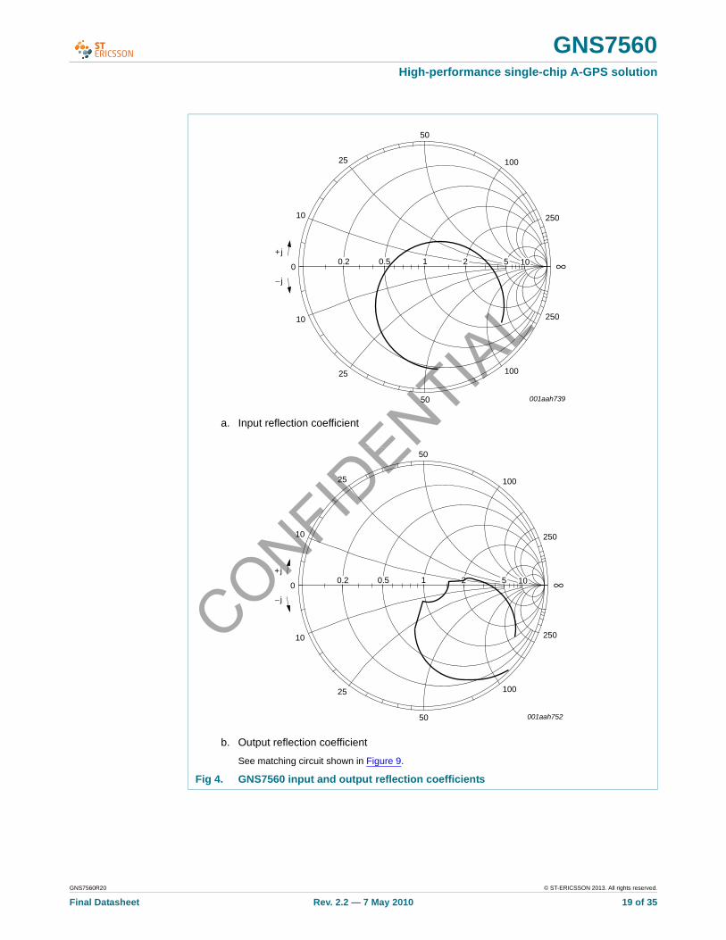
s112 input return loss see Figure 4 and Figure 5
- 13 - 15 - dB
CONFIDENTIA
L
GNS7560R20 © ST-ERICSSON 2013. All rights reserved.
Final Datasheet Rev. 2.2 — 7 May 2010 19 of 35
GNS7560High-performance single-chip A-GPS solution
a. Input reflection coefficient
b. Output reflection coefficient
See matching circuit shown in Figure 9.
Fig 4. GNS7560 input and output reflection coefficients
001aah739
10
25
50
100
250
10
25
50
100
250
050.50.2 21 10
+j
− j
∞
001aah752
10
25
50
100
250
10
25
50
100
250
050.50.2 21 10
+j
− j
∞

CONFIDENTIA
L
GNS7560R20 © ST-ERICSSON 2013. All rights reserved.
Final Datasheet Rev. 2.2 — 7 May 2010 20 of 35
GNS7560High-performance single-chip A-GPS solution
13. SSI host interface
The Slave Synchronous Serial Interface (SSI) is available as an optional interface which can be used instead of UART2 for interfacing an external host microprocessor.
a. Reverse transmission
b. Forward transmission
See matching circuit shown in Figure 9.
Fig 5. GNS7560 reverse and forward transmission
f (GHz)1.0 2.01.81.4 1.61.2
001aah750
−50
−46
−54
−42
−38
S(1, 2)(dB)
−58
f (GHz)1.0 2.01.81.4 1.61.2
001aah751
8
12
4
16
20
S(2, 1)(dB)
0
CONFIDENTIA
L
GNS7560R20 © ST-ERICSSON 2013. All rights reserved.
Final Datasheet Rev. 2.2 — 7 May 2010 21 of 35
GNS7560High-performance single-chip A-GPS solution
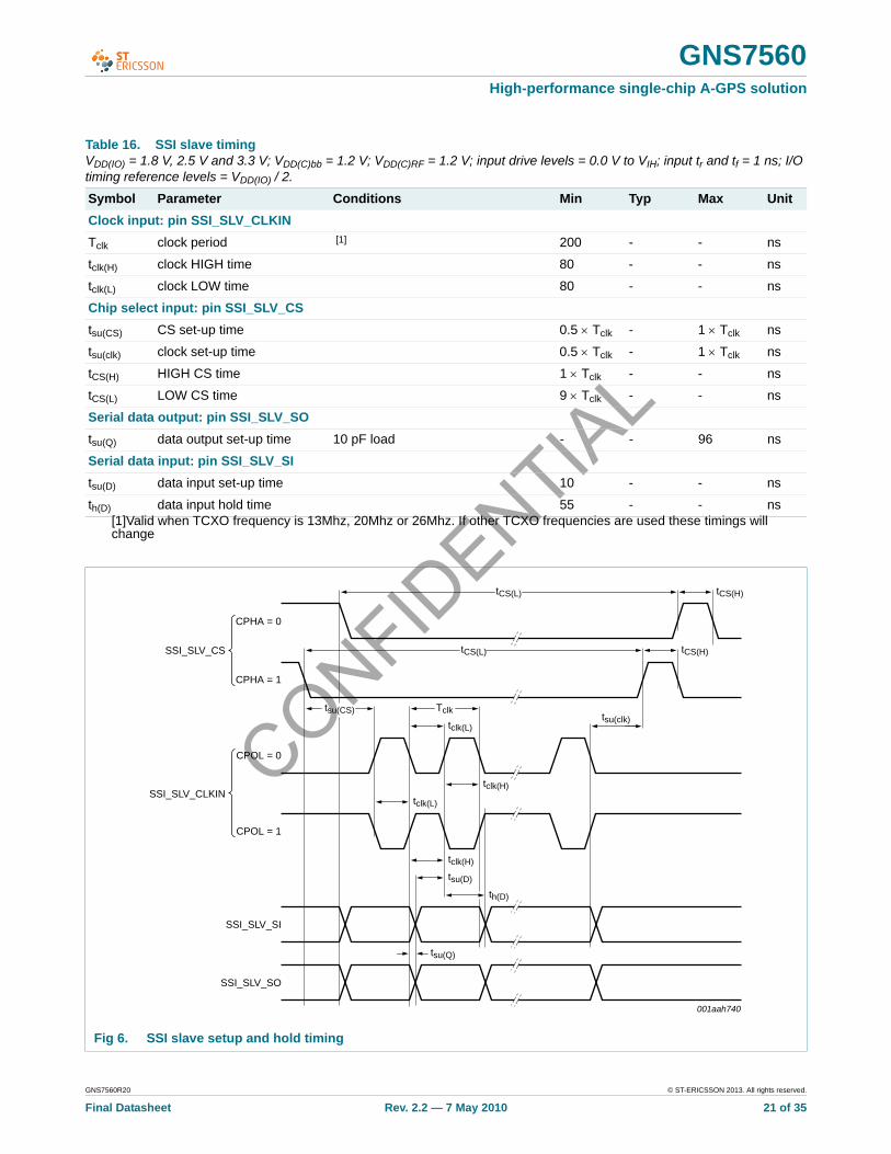
Table 16. SSI slave timingVDD(IO) = 1.8 V, 2.5 V and 3.3 V; VDD(C)bb = 1.2 V; VDD(C)RF = 1.2 V; input drive levels = 0.0 V to VIH; input tr and tf = 1 ns; I/O timing reference levels = VDD(IO) / 2.
Symbol Parameter Conditions Min Typ Max Unit
Clock input: pin SSI_SLV_CLKIN
Tclk clock period [1] 200 - - ns
tclk(H) clock HIGH time 80 - - ns
tclk(L) clock LOW time 80 - - ns
Chip select input: pin SSI_SLV_CS
tsu(CS) CS set-up time 0.5 Tclk - 1 Tclk ns
tsu(clk) clock set-up time 0.5 Tclk - 1 Tclk ns
tCS(H) HIGH CS time 1 Tclk - - ns
tCS(L) LOW CS time 9 Tclk - - ns
Serial data output: pin SSI_SLV_SO
tsu(Q) data output set-up time 10 pF load - - 96 ns
Serial data input: pin SSI_SLV_SI
tsu(D) data input set-up time 10 - - ns
th(D) data input hold time 55 - - ns[1]Valid when TCXO frequency is 13Mhz, 20Mhz or 26Mhz. If other TCXO frequencies are used these timings will change
Fig 6. SSI slave setup and hold timing
001aah740
tCS(H)tCS(L)
CPHA = 0
CPHA = 1
CPOL = 0
CPOL = 1
SSI_SLV_SI
SSI_SLV_CLKIN
SSI_SLV_CS
SSI_SLV_SO
tsu(CS) Tclk
tCS(H)tCS(L)
tclk(L)
tclk(L)
tclk(H)
tclk(H)
th(D)
tsu(Q)
tsu(D)
tsu(clk)

CONFIDENTIA
L
GNS7560R20 © ST-ERICSSON 2013. All rights reserved.
Final Datasheet Rev. 2.2 — 7 May 2010 22 of 35
GNS7560High-performance single-chip A-GPS solution
14. Reset input
[1] At VDD(C)bb = 1.08 V (minimum specified value).
[2] Reset delay must be matched to the start-up delays of the TCXO and optional external 32 kHz clock source, dependent on the components used. If the TCXO (PLLREFCLK is used then the power-up delay can be 7 cycles of the PLLREFCLK. In the case of a 26Mhz TCXO this time delay would be
[3] Based on seven 32 kHz clock periods,
Table 17. Reset timingVDD(IO) = 1.8 V, 2.5 V and 3.3 V; VDD(C)bb = 1.2 V; VDD(C)RF = 1.2 V; input drive levels = 0.0 V to VIH; input tr and tf = 1 ns; I/O timing reference levels = VDD(IO) / 2.
Symbol Parameter Conditions Min Typ Max Unit
tstab stabilization time 32 kHz oscillator [1] - 500 - ms
TCXO_IN oscillator - 100 - ms
td(pu) power-up delay time power rails valid to RST_N going HIGH; see Figure 7
[2] 500 - - ms
tWL(rst) reset pulse width LOW once sampled; see Figure 8 [3] 214 - - s
Fig 7. Reset timing
(1) VDD(C)bb = 1.08 V (minimum specified value).
Fig 8. Reset timing after power-up
001aah742
RST_N
tWL(rst)
001aah741
tstab
(1)
VDD(C)bb
CLK32KIN
RST_N

CONFIDENTIA
L
GNS7560R20 © ST-ERICSSON 2013. All rights reserved.
Final Datasheet Rev. 2.2 — 7 May 2010 23 of 35
GNS7560High-performance single-chip A-GPS solution
15. I/O Port timing
[1] 2 TCXO clock periods.
[2] 2 data clock periods.
Table 18. I/O port timingMeasured across the flat part of the waveform only; rise and fall parts not included.VDD(IO) = 1.8 V, 2.5 V and 3.3 V; VDD(C)bb = 1.2 V; VDD(C)RF = 1.2 V; input drive levels = 0.0 V to VIH; input tr and tf = 1 ns; I/O timing reference levels = VDD(IO) / 2.
Symbol Parameter Conditions Min Typ Max Unit
tw pulse width pin EXT_FRM_SYNC [1] 77 - - ns
pin EXT_DUTY_CYCLE [2] 23 - - ns
pin PULSE_OUT [2] 23 - - ns
CONFIDENTIA
L
GNS7560R20 © ST-ERICSSON 2013. All rights reserved.
Final Datasheet Rev. 2.2 — 7 May 2010 24 of 35
GNS7560High-performance single-chip A-GPS solution
16. Application information
(1) Refer to Table 19.
(2) Refer to Table 20.
(3) Refer to Table 21.
(4) Alternative circuits for front end, consult applications for additional information..
Fig 9. Typical application
001aah744
R2100 kΩ
33 Ω
R1
X2VDD(xtal)
32.768 kHz
C522 pF16 V
C622 pF16 V
IT2200
RFINPH11
C2C1
U1Murata SAFEB1G57FM0F00 ANT1
ANCG11G57SAA136
2 54
IN
GN
D
GN
D
GN
D
3
OUTM
OUTP
GNS7560
C51 nF
C4
X1
1 nF
B4
E2
D4
D2
E3
C6
C4
D5
F4
E4
B6
B5
C5
E1
GPIO[3]
EXT_FRM_SYNC
PULSE_OUT
UART2_RXD/SSI_SLV_CLKIN
UART2_TXD/SSI_SLV_SO
UART2_RXD/SSI_SLV_CLKIN
UART2_TXD/SSI_SLV_SOUART1_RXD
EXT_DUTY_CYCLE
PWM_OUT
UART1_TXD
LNA_EN
TCXO_EN
UART2_CTS/SSI_SLV_CS
UART2_RTS/SSI_SLV_SI
GPIO[12]
VD
DIO
2
VD
DIO
1
VD
DB
B3
VS
S3
A6
VD
DB
B2
B1
VS
S2
E6
VD
DB
B1
E5
VS
S1
A4
VS
S4
A3
VS
SP
LL
A2C1
VDD(C)bb(1.2 V)
VDD(IO)(1.8 V, 2.5 V, 3.3 V)
A5D1
RFINMJ1
SAWOUT/RFIN2J3
SAWINJ2
GNDRF2H2
GNDRF1G1
VDDRFG2
VDDANAH3
VSSANAJ4
GNDC1G4
GNDC2G5
VDDMSREG(1.2 V)
VDD(C)RFH6
VSSMSG6
VSSSX
TCXO_OUT
VDD(TCXO)
OUT
VCC
GND
J5
TE
STO
UT
G3
TE
ST
IN
H4
SX
TE
ST
H5
TC
XO
_IN
J6
MO
DE
3
B3
MO
DE
2
C3
MO
DE
1
MO
DE
0
A1
BO
OT
_SE
L2
B2
BO
OT
_SE
L1
F3
BO
OT
_SE
L0
F2
CLK
SE
LC
LKS
EL(
2)
(3) (1)
F1
DE
BU
G_B
OO
T
C2
CLK
32K
IN
D3
CLK
32K
OU
T
F5
RS
T_N
RST_NRST_N
F6 D6
2
4
1 3
L2
22 nH 2 %
L1
C30.5 pF
22 nH 2 %
ANT−
ANT+DIFFERENTIAL
GPSANTENNA
n.c.
23
1TUNE
ANT
(4)
GND
GND
GND1
42
OUT
U2(5)
SAFEB1G57KE0F00
5
3
IN
RFINP
RFINM
SAWOUT/RFIN2
SAWIN
Optional configuration - consult with Applications support
CONFIDENTIA
L
GNS7560R20 © ST-ERICSSON 2013. All rights reserved.
Final Datasheet Rev. 2.2 — 7 May 2010 25 of 35
GNS7560High-performance single-chip A-GPS solution
[1] Patch code.
Table 19. BOOT_SEL[2:0] settings
Frequency (MHz) Pin
BOOT_SEL2 BOOT_SEL1 BOOT_SEL0
13 LOW LOW LOW
16.368 LOW LOW HIGH
16.8 LOW HIGH LOW
19.2 LOW HIGH HIGH
19.68 HIGH LOW LOW
20 HIGH LOW HIGH
26 HIGH HIGH LOW[1] HIGH HIGH HIGH
Table 20. CLKSEL settings
Clock source Pin CLKSEL
Internal PLL clock LOW
External 32 kHz clock HIGH
Table 21. MODE[3:0] settings
Host interface Pin
MODE3 MODE2 MODE1 MODE0
UART1 and UART2 HIGH LOW LOW LOW
Slave SSI HIGH LOW LOW HIGH

CONFIDENTIA
L
GNS7560R20 © ST-ERICSSON 2013. All rights reserved.
Final Datasheet Rev. 2.2 — 7 May 2010 26 of 35
GNS7560High-performance single-chip A-GPS solution
17. Package outline
Fig 10. GNS7560ET2UM Package Outline

CONFIDENTIA
L
GNS7560R20 © ST-ERICSSON 2013. All rights reserved.
Final Datasheet Rev. 2.2 — 7 May 2010 27 of 35
GNS7560High-performance single-chip A-GPS solution
Fig 11. GNS7560UK214TS WLCSP package

CONFIDENTIA
L
GNS7560R20 © ST-ERICSSON 2013. All rights reserved.
Final Datasheet Rev. 2.2 — 7 May 2010 28 of 35
GNS7560High-performance single-chip A-GPS solution
18. Package Marking Information
18.1 BGA Marking information
18.2 WLCSP Marking information
19. Abbreviations
Marking Content
Line A : 7560/N2Line B: PPLLLWXLine C: LFTFYWW
Where; PP is Assembly plant (7B for ATP) LLL is to be replaced by trace code WX is wafer fab code (9R for TSMC14) LF is the RoHS code , “G” for Halogenated substrate “D” for Halogen Free (HF) substrate TF is the Testing and Finishing Production Area Code (78 for STC) YWW is to be replaced by actual date code.
Marking Content
Line A : 7560/14Line B: PPLLLWXLine C: LFTFYWWLine D: ST-E 2
Where; PP indicates Assembly plant (AA for ASE) LLL is to be replaced by traceability code WX is wafer fab code (9R for TSMC14) LF is the RoHS code (“D” for Halogen Free) TF is the Testing and Finishing Production Area Code (AA for ASE, AX for APK) YWW is to be replaced by actual date code.
Table 22. Abbreviations
Acronym Description
ADC Analog-to-Digital Converter
API Application Programming Interface
BGA Ball Grid Array
CDMA Code Division Multiple Access
CONFIDENTIA
L
GNS7560R20 © ST-ERICSSON 2013. All rights reserved.
Final Datasheet Rev. 2.2 — 7 May 2010 29 of 35
GNS7560High-performance single-chip A-GPS solution
20. Revision history
CS Chip Select
DSP Digital Signal Processor
EDGE Enhanced Data rates for GSM Evolution
GPIO General Purpose Input Output
GPRS General Packet Radio Service
GPS Global Positioning System
GSM Global System for Mobile communications
IF Intermediate Frequency
L1 L-band frequency 1 (centred at 1575 MHz)
LDO Low DropOut
LNA Low-Noise Amplifier
LO Local Oscillator
NCO Numerical-Controlled Oscillator
NVRAM Non-Volatile Random Access Memory
OS Operating System
PCB Printed-Circuit Board
PLL Phase-Locked Loop
PWM Pulse-Width Modulator
RFFE Radio Frequency Front-End
RMS Root-Mean-Square
SAW Surface Acoustic Wave
SMD Surface-Mount Device
SPI Serial Peripheral Interface
SSI Serial Synchronous Interface
SUPL Secure User Plane Location
SV Satellite Vehicle
TCXO Temperature-Controlled Crystal Oscillator
UART Universal Asynchronous Receiver Transmitter
UMTS Universal Mobile Telecommunications System
VCO Voltage-Controlled Oscillator
WCDMA Wideband Code Division Multiple Access
WLCSP Wafer-Level Chip Scale Package
Table 22. Abbreviations …continued
Acronym Description
Table 23. Revision history
Document ID Release date Data sheet status Change notice Supersedes
GNS7560_1 20080507 Objective data sheet - -
GNS7560_2 20081104 Preliminary data sheet
GNS7560_5 20081222 Minor updates to Table 10
GNS7560_8 20090519 Converted to STE format

CONFIDENTIA
L
GNS7560R20 © ST-ERICSSON 2013. All rights reserved.
Final Datasheet Rev. 2.2 — 7 May 2010 30 of 35
GNS7560High-performance single-chip A-GPS solution
GNS7560_20 20090701 Order numbers and order quantity updated
GNS7560_21 20100303 CLK32 & TCXO section improvements
GNS7560_22 20100403 Addtional order codes added & die marking section added
Table 23. Revision history …continued
Document ID Release date Data sheet status Change notice Supersedes

CONFIDENTIA
L
GNS7560R20 © ST-ERICSSON 2013. All rights reserved.
Final Datasheet Rev. 2.2 — 7 May 2010 31 of 35
GNS7560High-performance single-chip A-GPS solution
Notes

CONFIDENTIA
L
GNS7560R20 © ST-ERICSSON 2013. All rights reserved.
Final Datasheet Rev. 2.2 — 7 May 2010 32 of 35
GNS7560High-performance single-chip A-GPS solution
21. Index
1 General description . . . . . . . . . . . . . . . . . . . . . . . . . . . . . . . . . . . . . . . . . . . 1
2 Features . . . . . . . . . . . . . . . . . . . . . . . . . . . . . . . . . . . . . . . . . . . . . . . . . . . . 1
3 Applications . . . . . . . . . . . . . . . . . . . . . . . . . . . . . . . . . . . . . . . . . . . . . . . . . 2
4 Ordering information. . . . . . . . . . . . . . . . . . . . . . . . . . . . . . . . . . . . . . . . . . 2
5 Block diagram . . . . . . . . . . . . . . . . . . . . . . . . . . . . . . . . . . . . . . . . . . . . . . . 2
6 Functional diagram . . . . . . . . . . . . . . . . . . . . . . . . . . . . . . . . . . . . . . . . . . . 3
7 Pinning information. . . . . . . . . . . . . . . . . . . . . . . . . . . . . . . . . . . . . . . . . . . 47.1 Pinning . . . . . . . . . . . . . . . . . . . . . . . . . . . . . . . . . . . . . . . . . . . . . . . . . . . . 4
8 Functional description . . . . . . . . . . . . . . . . . . . . . . . . . . . . . . . . . . . . . . . . 78.1 System overview . . . . . . . . . . . . . . . . . . . . . . . . . . . . . . . . . . . . . . . . . . . . 78.1.1 Receiver section . . . . . . . . . . . . . . . . . . . . . . . . . . . . . . . . . . . . . . . . . . . . . 88.2 GPS performance. . . . . . . . . . . . . . . . . . . . . . . . . . . . . . . . . . . . . . . . . . . . 88.2.1 Positional accuracy. . . . . . . . . . . . . . . . . . . . . . . . . . . . . . . . . . . . . . . . . . . 88.2.2 Additional GPS-related features . . . . . . . . . . . . . . . . . . . . . . . . . . . . . . . . . 98.3 Additional features . . . . . . . . . . . . . . . . . . . . . . . . . . . . . . . . . . . . . . . . . . . 98.4 RF front end . . . . . . . . . . . . . . . . . . . . . . . . . . . . . . . . . . . . . . . . . . . . . . . . 98.5 GPS baseband . . . . . . . . . . . . . . . . . . . . . . . . . . . . . . . . . . . . . . . . . . . . . . 98.5.1 Overview. . . . . . . . . . . . . . . . . . . . . . . . . . . . . . . . . . . . . . . . . . . . . . . . . . . 98.5.2 Embedded DSP firmware . . . . . . . . . . . . . . . . . . . . . . . . . . . . . . . . . . . . . . 108.5.3 Interface between GNS7560 and host-based navigation software. . . . . . . 108.6 Host-based navigation software . . . . . . . . . . . . . . . . . . . . . . . . . . . . . . . . . 108.7 Clocks. . . . . . . . . . . . . . . . . . . . . . . . . . . . . . . . . . . . . . . . . . . . . . . . . . . . . 118.7.1 TCXO clock input . . . . . . . . . . . . . . . . . . . . . . . . . . . . . . . . . . . . . . . . . . . . 118.7.2 Low-power clock counter . . . . . . . . . . . . . . . . . . . . . . . . . . . . . . . . . . . . . . 128.8 Operating modes . . . . . . . . . . . . . . . . . . . . . . . . . . . . . . . . . . . . . . . . . . . . 128.9 UART interfaces . . . . . . . . . . . . . . . . . . . . . . . . . . . . . . . . . . . . . . . . . . . . . 13
9 Limiting values. . . . . . . . . . . . . . . . . . . . . . . . . . . . . . . . . . . . . . . . . . . . . . . 13
10 Recommended operating conditions . . . . . . . . . . . . . . . . . . . . . . . . . . . . 13
11 Characteristics. . . . . . . . . . . . . . . . . . . . . . . . . . . . . . . . . . . . . . . . . . . . . . . 14
12 Dynamic characteristics . . . . . . . . . . . . . . . . . . . . . . . . . . . . . . . . . . . . . . . 1813 SSI host interface . . . . . . . . . . . . . . . . . . . . . . . . . . . . . . . . . . . . . . . . . . . . 2014 Reset input . . . . . . . . . . . . . . . . . . . . . . . . . . . . . . . . . . . . . . . . . . . . . . . . . 2215 I/O Port timing. . . . . . . . . . . . . . . . . . . . . . . . . . . . . . . . . . . . . . . . . . . . . . . 23
16 Application information . . . . . . . . . . . . . . . . . . . . . . . . . . . . . . . . . . . . . . . 24
17 Package outline . . . . . . . . . . . . . . . . . . . . . . . . . . . . . . . . . . . . . . . . . . . . . . 26
18 Package Marking Information. . . . . . . . . . . . . . . . . . . . . . . . . . . . . . . . . . . 2818.1 BGA Marking information . . . . . . . . . . . . . . . . . . . . . . . . . . . . . . . . . . . . . . 2818.2 WLCSP Marking information . . . . . . . . . . . . . . . . . . . . . . . . . . . . . . . . . . . 28
19 Abbreviations. . . . . . . . . . . . . . . . . . . . . . . . . . . . . . . . . . . . . . . . . . . . . . . . 28
20 Revision history. . . . . . . . . . . . . . . . . . . . . . . . . . . . . . . . . . . . . . . . . . . . . . 29
21 Index . . . . . . . . . . . . . . . . . . . . . . . . . . . . . . . . . . . . . . . . . . . . . . . . . . . . . . . 32
22 Tables . . . . . . . . . . . . . . . . . . . . . . . . . . . . . . . . . . . . . . . . . . . . . . . . . . . . . . 33
23 Figures . . . . . . . . . . . . . . . . . . . . . . . . . . . . . . . . . . . . . . . . . . . . . . . . . . . . . 34

CONFIDENTIA
L
GNS7560R20 © ST-ERICSSON 2013. All rights reserved.
Final Datasheet Rev. 2.2 — 7 May 2010 33 of 35
GNS7560High-performance single-chip A-GPS solution
22. Tables
Table 1. Ordering information[1] . . . . . . . . . . . . . . . . . . . . . . . . . . . . . . . . . . . . . . . . . . . 2Table 2. Pin allocation table . . . . . . . . . . . . . . . . . . . . . . . . . . . . . . . . . . . . . . . . . . . . . . 4Table 3. Pin description . . . . . . . . . . . . . . . . . . . . . . . . . . . . . . . . . . . . . . . . . . . . . . . . . 5Table 4. Acquisition and tracking performance . . . . . . . . . . . . . . . . . . . . . . . . . . . . . . . 8Table 5. Positional accuracy . . . . . . . . . . . . . . . . . . . . . . . . . . . . . . . . . . . . . . . . . . . . . 8Table 6. GNS7560 typical power consumption . . . . . . . . . . . . . . . . . . . . . . . . . . . . . . 12Table 7. External LNA enable (LNA_EN) and TCXO enable (TCXO_EN) . . . . . . . . . . 13Table 8. Limiting values . . . . . . . . . . . . . . . . . . . . . . . . . . . . . . . . . . . . . . . . . . . . . . . . 13Table 9. Operating conditions . . . . . . . . . . . . . . . . . . . . . . . . . . . . . . . . . . . . . . . . . . . 14Table 10. Power supplies . . . . . . . . . . . . . . . . . . . . . . . . . . . . . . . . . . . . . . . . . . . . . . . 14Table 11. Digital input/output characteristics . . . . . . . . . . . . . . . . . . . . . . . . . . . . . . . . . 15Table 12. Clock inputs . . . . . . . . . . . . . . . . . . . . . . . . . . . . . . . . . . . . . . . . . . . . . . . . . . 17Table 13. 32kHz crystal oscillator characteristics . . . . . . . . . . . . . . . . . . . . . . . . . . . . . . 17Table 14. Example specification characteristics for TCXO. . . . . . . . . . . . . . . . . . . . . . . 17Table 15. RF input . . . . . . . . . . . . . . . . . . . . . . . . . . . . . . . . . . . . . . . . . . . . . . . . . . . . . 18Table 16. SSI slave timing . . . . . . . . . . . . . . . . . . . . . . . . . . . . . . . . . . . . . . . . . . . . . . . 21Table 17. Reset timing . . . . . . . . . . . . . . . . . . . . . . . . . . . . . . . . . . . . . . . . . . . . . . . . . . 22Table 18. I/O port timing . . . . . . . . . . . . . . . . . . . . . . . . . . . . . . . . . . . . . . . . . . . . . . . . 23Table 19. BOOT_SEL[2:0] settings . . . . . . . . . . . . . . . . . . . . . . . . . . . . . . . . . . . . . . . . 25Table 20. CLKSEL settings . . . . . . . . . . . . . . . . . . . . . . . . . . . . . . . . . . . . . . . . . . . . . . 25Table 21. MODE[3:0] settings . . . . . . . . . . . . . . . . . . . . . . . . . . . . . . . . . . . . . . . . . . . . 25Table 22. Abbreviations . . . . . . . . . . . . . . . . . . . . . . . . . . . . . . . . . . . . . . . . . . . . . . . . . 28Table 23. Revision history . . . . . . . . . . . . . . . . . . . . . . . . . . . . . . . . . . . . . . . . . . . . . . . 29

CONFIDENTIA
L
GNS7560R20 © ST-ERICSSON 2013. All rights reserved.
Final Datasheet Rev. 2.2 — 7 May 2010 34 of 35
GNS7560High-performance single-chip A-GPS solution
23. Figures
Fig 1. Block diagram . . . . . . . . . . . . . . . . . . . . . . . . . . . . . . . . . . . . . . . . . . . . . . . . . . .2Fig 2. Functional diagram . . . . . . . . . . . . . . . . . . . . . . . . . . . . . . . . . . . . . . . . . . . . . . .3Fig 3. Pin configuration; ball position (view from top) . . . . . . . . . . . . . . . . . . . . . . . . . .4Fig 4. GNS7560 input and output reflection coefficients . . . . . . . . . . . . . . . . . . . . . . .19Fig 5. GNS7560 reverse and forward transmission. . . . . . . . . . . . . . . . . . . . . . . . . . .20Fig 6. SSI slave setup and hold timing . . . . . . . . . . . . . . . . . . . . . . . . . . . . . . . . . . . .21Fig 7. Reset timing. . . . . . . . . . . . . . . . . . . . . . . . . . . . . . . . . . . . . . . . . . . . . . . . . . . .22Fig 8. Reset timing after power-up. . . . . . . . . . . . . . . . . . . . . . . . . . . . . . . . . . . . . . . .22Fig 9. Typical application . . . . . . . . . . . . . . . . . . . . . . . . . . . . . . . . . . . . . . . . . . . . . . .24Fig 10. GNS7560ET2UM Package Outline . . . . . . . . . . . . . . . . . . . . . . . . . . . . . . . . . .26Fig 11. GNS7560UK214TS WLCSP package . . . . . . . . . . . . . . . . . . . . . . . . . . . . . . . .27

CONFIDENTIA
L
GNS7560R20 © ST-ERICSSON 2013. All rights reserved.
Final Datasheet Rev. 2.2 — 7 May 2010 35 of 35
GNS7560High-performance single-chip A-GPS solution
CONFIDENTIALITY OBLIGATIONS:
This document contains sensitive information.Its distribution is subject to the signature of an Non-Disclosure Agreement (NDA).It is classified “RESTRICTED DISTRIBUTIONCONFIDENTIAL”.
At all times you should comply with the following security rules(Refer to NDA for detailed obligations):
Do not copy or reproduce all or part of this documentKeep this document locked away
Further copies can be provided on a “need to know basis”, please contact your local ST-ERICSSON sales office.
Please Read Carefully:
The contents of this document are subject to change without prior notice. ST-Ericsson makes no representation or warranty of any naturewhatsoever (neither expressed nor implied) with respect to the matters addressed in this document, including but not limited to warranties ofmerchantability or fitness for a particular purpose, interpretability or interoperability or, against infringement of third party intellectual propertyrights, and in no event shall ST-Ericsson be liable to any party for any direct, indirect, incidental and or consequential damages and or losswhatsoever (including but not limited to monetary losses or loss of data), that might arise from the use of this document or the information in it.
ST-Ericsson and the ST-Ericsson logo are trademarks of the ST-Ericsson group of companies or used under a license from STMicroelectronics NV or Telefonaktiebolaget LM Ericsson.
All other names are the property of their respective owners.
© ST-Ericsson, 2009 - All rights reserved
Contact information at www.stericsson.com under Contacts
www.stericsson.com