gordon moore’s law - wordpress.comgave a presentation in which he reviewed his ear-lier forecast....
TRANSCRIPT

The Anderson School at UCLA POL-2003-03
Gordon Moore’s Law
Figure 1
Copyright © 2003 by Richard P. Rumelt. This case may be freely copied for instructional use at the Uni-versity of California. This case was written from public documents and interviews with various industry observers and experts. It was prepared by Professor Richard P. Rumelt with the assistance of Olivier Costa, M.B.A. class of 2002, The Anderson School at UCLA.

The Anderson School at UCLA POL-2003-03
he semiconductor industry was unique in the progress it had achieved since its in-ception. The cost reduction and performance increases had been continuous and phenomenal. In the mid-nineties, Gordon Moore (a founder of Intel) said that if
similar progress had been achieved in air transportation, then a commercial aircraft would cost $500, circle the earth in 20 minutes on five gallons of fuel, and weigh only a few pounds. Only the data storage industry had scaled so dramatically in so short a time. Moore was first asked to comment on the probable evolution of integrated circuits in 1965,2 when he was Fairchild’s Director of R&D. He wrote:
Reduced cost is one of the big attractions of integrated electronics, and the cost advantage continues to increase as the technology evolves toward the production of larger and larger circuit functions on a single semiconductor substrate. For simple circuits, the cost per component is nearly inversely pro-portional to the number of components, the result of the equivalent piece of semiconductor in the equivalent package containing more components. But as components are added, decreased yields more than compensate for the in-creased complexity, tending to raise the cost per component. Thus there is a minimum cost at any given time in the evolution of the technology. At present, it is reached when 50 components are used per circuit….The complexity for minimum component costs has increased at a rate of roughly a factor of two per year…. That means by 1975, the number of components per integrated circuit for minimum cost will be 65,000. I believe that such a large circuit can be built on a single wafer.
Note that Moore did not say that progress was meas-ured by the density of transistors per unit area, or by the cost of a transistor. Here, he argued that the num-ber of components that could be integrated onto one chip depended upon a balance between the savings from “cramming” and the costs of decreased yield. The size and component count of a chip, therefore, was an engineering and business decision that reflected the state of the technology. Progress could be measured by the number of components that could be squeezed onto a chip. Based on three or four data points, he forecast an annual doubling (Figure 2). Moore’s 1965 paper has been based on experience and a general faith in the industry’s ability to make de-vices ever smaller. In 1972, Dennard and Gaensslen of IBM developed a theory of MOSFET scaling. Their surprising result was that if the electric field strength over the gate were was held constant, simple reduction in scale of a MOSFET would work, and would produce improved performance on almost every dimension.3 In particu-lar, if the linear dimension of the transistor were cut in half, then the voltage necessary
2 G.E. Moore, “Cramming More Components onto Integrated Circuits, Electronics, 1965. 3 Reported in Dennard, et al., "Design of Ion-Implanted MOSFET's with Very Small Physical Dimensions," IEDM, 1974.
T
Figure 2 Moore’s 1965 Forecast
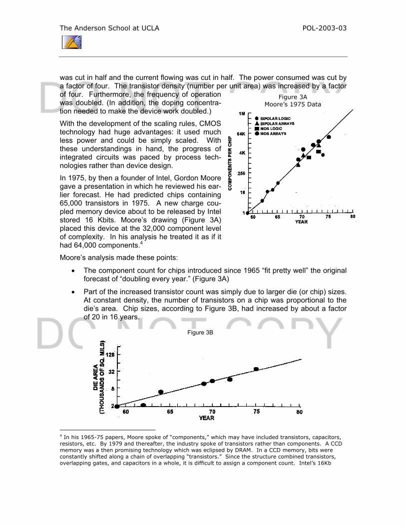
The Anderson School at UCLA POL-2003-03 was cut in half and the current flowing was cut in half. The power consumed was cut by a factor of four. The transistor density (number per unit area) was increased by a factor of four. Furthermore, the frequency of operation was doubled. (In addition, the doping concentra-tion needed to make the device work doubled.) With the development of the scaling rules, CMOS technology had huge advantages: it used much less power and could be simply scaled. With these understandings in hand, the progress of integrated circuits was paced by process tech-nologies rather than device design. In 1975, by then a founder of Intel, Gordon Moore gave a presentation in which he reviewed his ear-lier forecast. He had predicted chips containing 65,000 transistors in 1975. A new charge cou-pled memory device about to be released by Intel stored 16 Kbits. Moore’s drawing (Figure 3A) placed this device at the 32,000 component level of complexity. In his analysis he treated it as if it had 64,000 components.4 Moore’s analysis made these points:
• The component count for chips introduced since 1965 “fit pretty well” the original forecast of “doubling every year.” (Figure 3A)
• Part of the increased transistor count was simply due to larger die (or chip) sizes. At constant density, the number of transistors on a chip was proportional to the die’s area. Chip sizes, according to Figure 3B, had increased by about a factor of 20 in 16 years.
4 In his 1965-75 papers, Moore spoke of “components,” which may have included transistors, capacitors, resistors, etc. By 1979 and thereafter, the industry spoke of transistors rather than components. A CCD memory was a then promising technology which was eclipsed by DRAM. In a CCD memory, bits were constantly shifted along a chain of overlapping “transistors.” Since the structure combined transistors, overlapping gates, and capacitors in a whole, it is difficult to assign a component count. Intel’s 16Kb
Figure 3A Moore’s 1975 Data
Figure 3B

The Anderson School at UCLA POL-2003-03
• Part of the increased transistor count was due to higher density—more transis-tors per unit area. The transistor density was inversely proportional to the square of feature size, so that as feature size fell, density increased.5 Examining feature size trends (Exhibit 3C), Moore argued that feature size reductions had created a 32X increase in transistor density between 1961 and 1975.
• Putting the above three factors together, Moore could only account for a portion of the increase in transistor count he saw between 1959 and 1975 (Exhibit 3D). He attributed the remainder to “circuit and device cleverness.” In particular, he credited the advent of MOS devices and better isolation to greater packing densi-ties.
memory chip would have had 16,000 overlapping transistors and one could count another 16,000 capaci-tors, but that is not the practice in assessing DRAM. 5 Feature size was normally limited by cleanliness and lithography, and was usually measured by the mini-mum distance between parallel “lines” on the IC.
Figure 3C
Figure 3D

The Anderson School at UCLA POL-2003-03 Looking ahead, Moore forecast that there would be less and less opportunity for “clever-ness.” The complexity (component count) curve would slow down, he forecast. Within five years, the rate of progress would fall to a “doubling every two years.” Once again, in 1979, Moore revisited the issue of the progress in integrated circuit com-plexity.6 He restated his view that complexity of the most advanced chips had been doubling each year during the first 15 years of the industry and subsequently doubling every two years. However, he added some new observations. In particular, Moore noted that design costs were coming to dominate manufacturing costs. Design costs, he estimated, were inflating at 10 percent per year. In addition, there were increasing prob-lems in on-chip connections and packaging that limited the gains to improved transistor density. The rising costs of designing increasingly complex chips would have put a quick stop to progress in integrated circuits, he argued, if the calculator and memory not appeared:
In general, the semiconductor industry's efforts to solve its problems in the 1965-1968 era were not successful. The product definition crisis persisted and limited IC complexity through the mid-60s. Two things broke the crisis for semiconductor component manufacturer, though not necessarily for the main-frame computer manufacturer: the development of the calculator and the ad-vent of semiconductor memory devices.
Thus, Moore credited the microprocessor and associated memory devices with the con-tinuing progress of the industry. Without these products, demand would have been lim-ited to the sale of individual logic components or to the very expensive integrated chips needed by mainframes and aerospace applications. In essence, the microprocessor off-loaded the cost of logic design onto software engineers, and allowed semiconductor manufacturers to reap economies of producing standardized chips. Microprocessors, in turn, needed memory. The exploding demand for microprocessors and memory were the dynamo that drove “Silicon Valley.” Moore’s projection of exponential growth in transistor count per chip was dubbed “Moore’s Law” by Carver Mead, a Cal Tech semiconductor physicist. Moore’s Law was very widely, and incorrectly, stated as the rule that chip density will double each 18 months. As Moore himself noted,
I never said 18 months. I said one year, and then two years. One of my Intel colleagues changed it from the complexity of the chips to the performance of computers and decided that not only did you get a benefit from the doubling every two years but we were able to increase the clock frequency, too, so computer performance was actually doubling…. Moore's Law has been the name given to everything that changes exponentially in the industry…. if Gore invented the Internet, I invented the exponential.7
Whatever Gordon Moore originally meant, or said, the “double every 18 months” rule be-came a touchstone in Silicon Valley (See Figure 4). As one industry watcher put it8:
6 G.E. Moore, “VLSI: Some Fundamental Challenges,” IEEE Spectrum, 1979, pp. 30-37. 7 D.J. Yang, “On Moore’s Law and Fishing: Gordon Moore Speaks Out,” U.S. News Online, 2000.
8Malone, Michael S. 1996. "Chips Triumphant," Forbes ASAP, February 26, pp. 53-82.

The Anderson School at UCLA POL-2003-03
Moore's Law is important because it is the only stable ruler we have today. It's a sort of technological barometer. It very clearly tells you that if you take the information processing power you have today and multiply by two, that will be what your competition will be doing 18 months from now. And that is where you too will have to be.
The semiconductor industry’s chief coordinating instrument was the International Tech-nology Roadmap for Semiconductors (IRTS), produced by an international working group. This complex document provided a coordinated forecast of the detailed techno-logical characteristics of integrated circuits up to 15 years into the future. Specifically, the IRTS defined a new technology “node” as occurring when there was a 0.7X reduction in feature size (0.5X increase in density). This reduction in feature size was called scaling. IRTS claimed that during 1974-1999 the node cycle time was 2 years. It projected future nodes to occur every three years. Since its start in 1992, the IRTS made the assump-tion that
continued scaling of microelectronics would further reduce the cost per func-tion (averaging ~25% per year) and promote market growth for integrated cir-cuits (averaging ~17% per year). Thus, the Roadmap has been put together in the spirit of a challenge—essentially, “What technical capabilities need to be developed for the industry to continue to stay on Moore’s Law and other trends?”
The IRTS Roadmap was studied by everyone in the industry. For the challenges to be met, simultaneous investments in solving problems had to be made by mask-makers, process equipment designers, wafer producers, resist manufacturers, lithography equipment producers, device designers, test and packaging engineers, etc. The Roadmap provided not only a forecast of product characteristics, but a fairly detailed ex-planation of the technical challenges in each supplier area that would have to be met to keep the industry on the trend-line.
.
Figure 4 Moore’s Law Illustration on Intel Website

The Anderson School at UCLA POL-2003-03 Despite the mechanical aspect of the Roadmap forecast, many experts believed that Moore’s Law was more of a social than a physical phenomenon. Carver Mead offered this explanation of how Moore’s Law actually worked:
After it's [Moore's Law] happened long enough, people begin to talk about it in retrospect, and in retrospect it's really a curve that goes through some points and so it looks like a physical law and people talk about it that way. But actu-ally if you're living it, which I am, then it doesn't feel like a physical law. It's really a thing about human activity, it's about vision, it's about what you're al-lowed to believe. Because people are really limited by their beliefs, they limit themselves by what they allow themselves to believe what is possible. So here's an example where Gordon, when he made this observation early on, he really gave us permission to believe that it would keep going. And so some of us went off and did some calculations about it and said, 'Yes, it can keep going'. And that then gave other people permission to believe it could keep going. And [after believing it] for the last two or three generations, 'maybe I can believe it for a couple more, even though I can't see how to get there'…. The wonderful thing about it is that it is not a static law, it forces everyone to live in a dynamic, evolving world.9
The Mechanics of Moore’s Law
The increasing complexity of integrated circuits was driven by a constant reduction in the size of transistors and other components. Because of the scaling rules, designers kept track of the smallest feature that had to be carefully etched—calling it the feature size. Between 1971 and 2003, the feature size of transistors fell from 10 microns 10 to 0.1 mi-crons—a factor of 100 (Figure 5). Other things being equal, a reduction in feature size by a factor of 100 meant that transistor density (num-ber of transistors in a given area) in-creased by a factor of 100X100 = 10,000. That is, if other things were equal, a chip that held 3000 transis-tors in 1971 could hold 30 million in 2003. Integrated circuits were not individu-ally assembled. Instead, they were etched onto silicon wafers using processes that were more like print-ing or photography than mechanical
9 Carver A. Mead 1992. 10 A micron is one-millionth of one meter (one ten-thousandth of a millimeter) abbreviated as µm or sim-ply µ. There are 1000 nanometers in one micron, so 0.1 µm = 100 nm.
Figure 5 Feature Size Evolution

The Anderson School at UCLA POL-2003-03 assembly. In fact, over the period 1970-2000, the cost of processed silicon wafers had remained more or less constant at approximately $5 per cm2 (50 cents per mm2.) Since most of the cost of processing a wafer was independent of how many transistors it con-tained, the cost per transistor had fallen roughly inversely with transistor density. The relative constancy in the cost per square cm for wafer processing had been achieved in spite of the increasingly complex processes employed. This increased process complexity had been largely offset by increases in the diameter of the wafers used. Whereas the original Intel 4004 had been produced on a 2” (50 mm) wafer, 6” wa-fers were commonplace in the mid-1980s. By 1998, the bulk of industry production was on 8” (200 mm) wafers, and many firms were planning the conversion to 12” (300 mm) wafers. If the MOS scaling rules had applied perfectly, and had the cost per cm2 of silicon re-mained constant, down-scaling transistors by a factor of 100 would have reduced the cost per transistor by a factor of 10,000, reduced power consumed per transistor by a factor of 10,000, and increased operating frequency by a factor of 100. Although tech-nology buffs liked to point to each of these general trends as if they were separate tech-nological achievements, they were all a direct result of scaling. The scaling of devices, the continued reduction in feature size, pushed the semiconduc-tor industry towards amazing improvements in complexity and price. Exhibits 1 through 8 display data on the historical trends in microprocessor complexity, DRAM complexity, price trends, die sizes, and trends in defect density.
Pushing Lithography—Resolution Enhancement Technology
Optics is the science of light. The principles of lenses, imaging, and how light waves interfere with one another were well understood since the late 19th century. A central principle of op-tics was the criterion, developed by Lord Rayleigh, for the resolving power of an optical system. Rayleigh’s crite-rion was developed by considering the diffraction patterns of light. When light from a point source is focused by a lens, the image is not a perfect point. Instead, of being a point, or a simple disc, the image produced is a set of concentric rings of light and dark called an Airy Disc. In simple terms, small features of an image are blurred because the lens is finite. Figure 6 shows the Airy Discs produced on photographic film by one point source (above) and two points (below). As the size of the lens is increased, the Airy Disc be-comes more compact. With a sufficiently large lens (right) the Airy discs become small enough to resolve the two points. Rayleigh’s Criterion explained why a larger lens gave a sharper image. Larger telescopes and binoculars showed more details. Rayleigh’s
Figure 6 Airy Disc’s of Single (upper) and Binary (lower) Stars for
Increasing Lens Diameters

The Anderson School at UCLA POL-2003-03 Criterion also explained the resolving power of the human eye and helped define 20/20 vision. Replacing the problem of two stars with that of resolving two lines on a mask into two lines on a wafer, Rayleigh’s Criterion becomes:
1 1
sink kF
n NAλ λα
= =
where F is the feature size, λ is the wavelength of light forming the image, n is the index of refraction of the medium (n = 1 for air), α is the capture angle of the lens (light gather-ing ability) and k1 is a measure of the “complexity” of the photolithography system.
An optical system’s numerical aperture was defined as NA = n sin α and was never lar-ger than n. Similarly, physical principles required that k1 ≥ 0.5. Together, these con-straints implied F ≥ λ/2. Thus, laws of optics seemed to prohibit lithography of features separated by anything less than ½ of a wavelength of light. More practically, real-world optical systems tended to have NA = 0.75 and k1 ≈ 0.6, so the realistic spacing limit was closer to 1 wavelength of light.11
Normal light used in lithography had a wavelength of 0.5-0.6 µm. The idea that physics limited photolithography to feature sizes of ½ micron and larger was generally accepted in the early 1980s. In 1983 two Bell Laboratories scientists stated that
After consideration of all factors which limit resolution such as exposure hard-ware, resist systems, registration, alignment, and line width control, there is a general consensus that the useful resolution limit of photolithography may lie somewhere between 0.4 and 0.8 um and depends on such factors as the im-plementation of short wavelength UV and the ability to accurately place im-ages from a projection tool onto a silicon wafer.12
Some experts were echoing this view into the early 1990s. For example, Tennant and Hielmieier13 wrote: “Most experts agree that the exponential decrease in the minimum line width of optical lithography (the current method for "printing" circuits on silicon) will probably reach a limit of about .25 micron in the 1990's...minimum line widths for high-volume ICs will not get much smaller than .25 micron.” Given these hard limits, it seemed clear to many that the industry would have to push beyond visible light and use shorter wavelength ultraviolet light or even x-rays, eventu-ally moving to electron-beam lithography. The problems with such moves were im-mense—most materials were opaque to ultraviolet light, including class and quartz. Lenses would have to be replaced by focusing mirrors. Additionally, whole new classes of resists would have to be developed. 11 The limitation is often stated as restricting the minimum feature size. This is not strictly true. By using a photoresist that is responsive to only the most intense light, a single feature of arbitrarily small size can be imaged. However, the Rayleigh Criterion limits the minimum spacing between two features. 12 L. F. Thompson and M. J. Bowden, "The Lithographic Process: The Physics," in Introduction to Micro-lithography : Theory, Materials, and Processing, Thompson and Bowden, eds., based on a workshop sponsored by the ACS Division of Organic Coatings and Plastics Chemistry at the 185th Meeting of the American Chemical Society, Seattle, Washington, March 20-25, 1983. 13 Harry Tennant and George H. Heilmeier, "Knowledge and Equality: Harnessing the Tides of Information Abundance," in Technology 2001: The Future of Computing and Communications, Derek Leebaert (Editor), Cambridge: The MIT Press, 1991.

The Anderson School at UCLA POL-2003-03 Despite considerable investment in x-ray and electron-beam techniques, there were a number of engineering developments that confounded the predictions of physicists. Three developments—high-contrast photoresists, optical proximity correction (OPC) and phase-shift masks (PSM)—were the most important. All broke the hard logic of the Rayleigh Criterion by changing the problem.
High-Contrast Photoresists Consider the problem of imaging a series of rec-tangular lines. If the distance between the lines was on the order of a wave length of light, dif-fraction would make the image of the lines blurred and indistinct and the spaces between them would not be reliably reproduced. How-ever, a very high contrast photoresist could still produce sharp-edged lines after development! Figure 7 displays this phenomenon, showing how very sharp edges in high-contrast resist could be recovered even when imaging rectan-gles on a 250 nm pitch with 248 nm light. The key to this effect was the chemically ampli-fied resist, developed through collaborative work between IBM and universities.14 In this system, light creates a catalyst which drives a second chemical reaction during the bake phase. The amplification occurs in that one photon of light leads to alterations in many atoms rather than just one. This ratio is called the quantum effi-ciency, and chemical amplification pushed it above unity. Commenting on the power of the new photoresists, Lloyd Harriott, head of advanced lithography at Lucent Technology’s Bell Labs, said “The chemists saved the day. Improvements in deep UV photoresists were so high-contrast you could pull out im-ages better than people thought." Ultimately, this technique worked because the patterns being imaged were binary: the desired image was either “on” or “off” at each position, there was nothing “soft” in the pattern to be imaged. The negative aspect of these new chemicals was their extreme sensitivity to low concentration chemicals in the air due to paint, dust, etc.
OPC Optical proximity correction (OPC) methods were first developed in the 1970s, but were not commonly used until the 1990s. The traditional way of projecting a rectangular shape onto the resist was to build a mask with a rectangular pattern on it and project its image. However, as the size of the rectangle became comparable to a wavelength of light, the resultant image was blurred (Figure 8). However, by understanding and pre-dicting the effects of diffraction, engineers could build a mask with a non-rectangular pat- 14 Especially Grant Willson at IBM, now at the University of Texas, Austin and Jean Frechet, University of Ottawa and UC Berkeley.
Figure 7 High Contrast Photoresist Adds Sharp-
ness

The Anderson School at UCLA POL-2003-03 tern which would “blur” into a rectangle! The left panel of Figure 8 shows what happened when a 180 nm fea-ture was submitted to 250 nm technology; the result was a blurred image with the center section necked-down. By altering the mask, however, a perfectly pre-sentable 180 nm feature could be produced with 250 nm technology.
PSM As engineers began to work with this idea, they also began to adopt phase-shift mask (PSM) techniques. Theoretically understood since 1982, these methods were developed by leading Japa-nese mask suppliers, working in cooperation with their DRAM customers. This tech-nique could produce even finer features than OPC, but was much more complex to im-plement. Phase-shift masks were built out of more than one kind of material, say glass and quartz. Instead of controlling diffraction patterns with specific shapes, as in OPC, phase-shift methods used the differing thicknesses of materials to induce sharper corners and edges in the image. Figure 9 shows the operation of a PSM. Light representing one feature shines through two slits in the mask. The distance between the slits is less than 1 micron, producing wa-fer images less than 0.25 micron apart. When the right slit has an additional quartz thickness added, the light emerging is 180 degrees out of phase with the light from the left slit. Light that is perfectly out of phase cancels, creating a dark area where the light
from both slits overlap. Thus, the PSM creates two separate images rather than one blurry composite. RET methods reduced the effective or implied value of k1 being achieved below the “theoretical” limit of ½. Classical optics had predicted that 248 nm
light could not create features of less than 124 nm, even using perfect equipment. Nev-ertheless, by 2003, 248 nm light waves were creating image features smaller than 120 nm on a production basis. Still, most observers believed that it would not be possible to push k1 below ¼. If that were true, and if Moore’s law was to continue, optical lithogra-phy would be left behind in 2007. Some firms were again investing considerable funds in next-generation lithography. Intel led a consortium pressing for 13 nm soft x-ray (ex-treme ultra-violet) technology. IBM was advancing electron-beam methods. Other technologists, however, believed that there really were no limits to what could be done
Figure 8
Figure 9

The Anderson School at UCLA POL-2003-03 nologists, however, believed that there really were no limits to what could be done with optical lithography and cleverness. S. Brueck (University of New Mexico), argued that much more could be achieved with optical lithography. Enough, in fact, to reach the scaling limits of current materials and device designs. In particular, he pointed to laser interference patterns with very small pitches, immersion lithography (increasing the index of refraction n by 50%), and proc-essing tricks. For example, after putting lines onto a resist, treatment with oxygen could thin them well below the limits achieved with lithography alone. In 2003, Intel’s most ad-vanced processes used this technique to achieve critical 90 nm spacings.
Yield Scaling
The trend had been for the critical dimensions of devices to become ever smaller, so that the size of “killer” particles was also diminishing. Smaller particles, in turn, were less subject to Brownian flotation, and fell faster in air. Thus, settling time was diminishing as the industry progressed. Kita-jima and Shiramizu estimated that whereas the time for one killer particle to settle on a wafer was 1 minute in 1990, it was only a few seconds in 2003. Figure 11 shows Kitajima and Shiramizu’s measurements of cumulative particle densities on a wafer as functions of particle size. Contaminant particles caused defects on the wa-fer that reduced the number good chips—the yield. Standard practice in the industry was to
Figure 10 Evolution of Photolithography
Figure 11
0 V, 100 V and 500 V are the electrostatic potential of the wafer. (a) wafer surface is upward (dotted line). (b) wafer surface vertical (solid line).

The Anderson School at UCLA POL-2003-03 relate yield to the expected number of killer defects per mm2 (D , the defect density) and the active area of a die Ad . The expected number γ of killer defects on one particular die was
dA Dγ = . (1)
The probability of failure is the probability that γ ≥ 1. Assuming that (1) represented the mean of a gamma distribution, yield (the probability that γ = 0) was given by
1 1dA DYα αγ
α α
− − = + = +
. (2)
This was known as the “negative binomial” model in the industry. Here, α was the “clus-tering” parameter and reflected the degree to which particle positions were correlated. Normally, α had a value in the neighborhood of 2, but ranged from 0.3 to 5. The other common yield model in use was the “Murphy” model:
2
1 eYγ
γ
− −=
. (3)
Both models imply that yield will fall as the area of a die is increased. Given a random pattern of defects on a wafer, the larger the dice, the higher the chance that any particu-lar die will have a defect. Although helpful for controlling a given process, (2) and (3) were not very useful for pre-dicting the yield of a new process at a new scale. The problem was that the defect den-sity D was given as a constant, but it actually depended upon the minimum feature size and the distribution of particle sizes. To deal with the problem of varying feature sizes and, consequently, killer particle sizes, it was generally assumed that cumulative particle densities followed a power law. That is, given an area of surface, the number Nx of particles with a diameter of X or greater was proportional to 1/X q. Simply stated, there were q times as many killer particles for ½ micron features as there were for 1 micron features. Consequently, moving to smaller dies with smaller feature sizes might not reduce yields after all. Given the power law, the effects of scaling and increases in transistor count could be accommodated with this formula:
2
1 11 0
0 0
qT FT F
γ γ−
=
. (4)
Here, an “original” die with T0 transistors and feature size F0 had expected defect rate γ0. The yield on the original process was Y0 = (1 + γ0/α) -α . When the process was scaled to a new feature size F1, and the chip re-engineered to a new transistor count T1, the new expected defect rate γ1 was given by (4) and the new yield by Y1 = (1 + γ1/α) -α .

The Anderson School at UCLA POL-2003-03 Stapper,15 of IBM Labs, claimed that empirical work had shown that q lay between 1.5 and 3.5, and that q = 2 was a best estimate for most data. If q was 2, as claimed, then
11 0
0
TT
γ γ
=
, (5)
which Stapper called the “conservation of yield.” By that, he meant that if the distribution of defect sizes followed the inverse-square power law, then the yield of a wafer was not effected by a change in scale (as long as the transistor count per chip was kept the same.) Equation (5) explained both the benefits and issues with scaling down: with a reduction in scale there would be no reduction in yield using the same design, but a more integrated design would depress yields, making it important to reduce the base de-fect density.
Fundamental Limits to Scaling
To a large extent, the operation of Moore’s Law during the period 1965-2003 had been driven by MOS scaling, pushing the limits of optical lithography, and ever cleaner clean-rooms. Each of these processes did have some fundamental limits. The most severe were those of the transistor itself. One such limit was the thickness of the oxide insulating barrier between the gate elec-trode and the silicon material beneath. By 2003 this layer was only a few atoms thick. Making it thinner ran into the essential granularity of matter—it was composed of atoms which were not divisible. Oxide layers of 1 or 2 atoms would also be susceptible to quantum tunneling—they would no longer insulate. A second limit was that scaling was being achieved by increasing the concentration of dopants (e.g., boron, phosphorus). As these concentrations reached very high levels, there were no longer enough spaces left in the crystal for new dopants, so no new con-ductors (electrons or holes) were added. A third factor was that the scaling rules depended upon reducing the operating voltage in proportion to the scale. But voltages less than about 0.25v appeared unachievable unless devices were super-cooled. At normal temperatures, such small voltages began to compete with background electron “noise” and ceased to define logical levels of “1” and “0.” Despite these limits, many technologists had faith that “something would happen.” At a very general level, Moore’s Law could be taken to refer to computing power and cost. In such terms, many believed that it would continue to operate despite apparent limits im-posed. If there were limits to scaling MOS devices, then other kinds of devices would be found. If there were limits to lithography, then other ways of manipulating matter would be developed.
15 Charles H. Stapper, “The Defect Sensitivity Effect of Memory Chips,” IEEE Journal of Solid-State Cir-cuits, 1986, pp. 193-98. His p refers to the density distribution and is q + 1.

The Anderson School at UCLA POL-2003-03
Exhibit 1
Intel Microprocessors Model and Sub-Models
Model Speed MHz IntroDate
Process Microns
DieSize Sq-mm Voltage
Transistors Millions
4004 0.108 11/1/1971 10.000 13.5 0.0023 8008 0.200 4/1/1972 10.000 15.2 0.0035 8080 2 4/1/1974 6.000 20.0 0.0045 8085 5 3/1/1976 3.000 0.0065 8086 10 6/8/1978 3.000 28.6 0.0290 8088 8 6/1/1979 3.000 0.0290 80286 12 2/1/1982 1.500 68.7 0.1340 386DX 16 10/17/1985 1.250 104 0.2750 386DX 20 2/16/1987 1.250 0.2750 386DX 16 4/4/1988 1.250 0.2750 386SX 16 6/16/1988 1.250 0.2750 386SX 20 1/25/1989 1.250 0.2750 486DX 25 4/10/1989 0.800 163 1.20 386DX 33 4/10/1989 1.250 0.2750 486DX 33 5/7/1990 0.800 1.20 386SL 20 10/15/1990 1.000 0.86 486DX 50 6/24/1991 1.000 1.20 486SX 16 9/16/1991 0.800 0.90 386SL 25 9/30/1991 1.000 0.86 DX2 50 3/3/1992 0.800 1.20 DX2 66 8/10/1992 0.800 1.20 486SX 33 9/21/1992 0.800 1.19 386SX 33 10/26/1992 1.250 0.2750 486SL 33 11/9/1992 0.800 1.40 Pent. 66 3/22/1993 0.800 264 3.1 Pent. 100 3/7/1994 0.600 3.2 DX4 100 3/7/1994 0.600 1.60 Pent. 75 10/10/1994 0.600 3.2 Pent. 120 3/27/1995 0.600 3.2 Pent. 133 6/1/1995 0.350 3.3 Pent.Pro 200 11/1/1995 0.350 310 5.5 Pent. 166 1/4/1996 0.350 3.3 Pent. 200 6/10/1996 0.350 3.3 Pent. with MMX 200 1/8/1997 0.350 4.5 Pent.II 300 5/7/1997 0.350 209 7.5 Pent. with MMX 233 6/2/1997 0.350 4.5 Pent.Pro 200 8/18/1997 0.350 5.5 Pent. with MMX 233 9/9/1997 0.250 4.5 Pent. with MMX 266 1/12/1998 0.250 4.5 Pent.II 333 1/26/1998 0.250 7.5

The Anderson School at UCLA POL-2003-03 Mob. Pent.II 266 4/2/1998 0.250 1.7 7.5 Pent.II 400 4/15/1998 0.250 7.5 Pent.II Xeon 400 6/29/1998 0.250 7.5 Pent.II 450 8/24/1998 0.250 7.5 Mob. Pent.II 300 9/9/1998 0.250 1.6 7.5 Pent.II Xeon 450 10/6/1998 0.250 7.5 Pent.II Xeon 450 1/5/1999 0.250 7.5 Pent. with MMX 300 1/7/1999 0.250 4.5 Mob. Celeron 266 1/25/1999 0.250 1.6 18.9 Mob. Pent.II 366 1/25/1999 0.250 1.6 27.4 Pent. III 500 2/26/1999 0.250 128 9.5 Pent.III Xeon 550 3/17/1999 0.250 9.5 Mob. Celeron 333 4/5/1999 0.250 1.6 18.9 Pent. III 450 5/17/1999 0.250 9.5 Mob. Celeron 366 5/17/1999 0.250 153 1.6 18.9 Mob. Celeron 400 6/14/1999 0.250 1.6 18.9 Mob. Pent.II 400 6/14/1999 0.180 1.5 27.4 Mob. Pent.II 400 6/14/1999 0.250 1.55 27.4 Pent. III 600 8/2/1999 0.250 9.5 Mob. Celeron 466 9/15/1999 0.250 1.9 18.9 Pent. III 733 10/25/1999 0.180 106 28.0 Mob. Pent.III 500 10/25/1999 0.180 1.6 28.0 Pent.III Xeon 733 10/25/1999 0.180 28.0 Pent.III Xeon 667 1/12/2000 0.180 28.0 Mob. Pent.III SS
650 1/18/2000 0.180 28.0
Pent. III 1,000 3/8/2000 0.180 28.0 Pent. III 850 3/20/2000 0.180 28.0 Pent.III Xeon 866 4/10/2000 0.180 28.0 Mob. Pent.III SS
700 4/24/2000 0.180 1.35 28.0
Pent.III Xeon 700 5/22/2000 0.180 28.0 Pent. III 933 5/24/2000 0.180 28.0 Pent.III Xeon 933 5/24/2000 0.180 28.0 LV Mob. Pent.III SS
500 6/19/2000 0.180 28.0
Mob. Pent.III SS
750 6/19/2000 0.180 28.0
Mob. Pent.III SS
750 9/25/2000 0.180 28.0
Pent.4 1,500 11/20/2000 0.180 224 42.0 ULV Mob. Pent.III SS
500 1/30/2001 0.130 44.0
LV Mob. Pent.III SS
700 2/27/2001 0.180 28.0
Mob. Pent.III SS
1,000 3/19/2001 0.180 1.35 28.0
LV Pent.III (Ap-plied)
700 3/19/2001 0.180 1.35 28.0
Pent.III Xeon 900 3/21/2001 0.180 28.0

The Anderson School at UCLA POL-2003-03 Pent.4 1,700 4/23/2001 0.180 42.0 Itanium 800 5/1/2001 0.180 25.0 Xeon 1,400 5/21/2001 0.180 42.0 LV Mob. Pent.III SS
750 5/21/2001 0.180 1.1 28.0
Pent.4 1,600 7/2/2001 0.180 42.0 Mob. Pent.III -M 1,000 7/30/2001 0.130 44.0 Mob. Pent.III -M 933 7/30/2001 0.130 1.15 28.0 Pent.4 2,000 8/27/2001 0.180 42.0 Xeon 2,000 9/25/2001 0.180 42.0 Mob. Pent.III -M 1,200 10/1/2001 0.130 1.4 44.0 ULV Mob. Pent.III
700 11/13/2001 0.130 1.1 44.0
Pent. III for Serv-ers
1,400 1/8/2002 0.130 44.0
ULV Mob. Pent.III SS
750 1/21/2002 0.130 1.1 44.0
LV Mob. Pent.III -M SS
533 1/21/2002 0.130 44.0
Mob. Pent.4 -M 1,700 3/4/2002 0.130 55.0 Xeon MP 1,600 3/12/2002 0.180 108.0 Pent.4 2,000 4/2/2002 0.130 55.0 Xeon 2,000 4/3/2002 0.130 55.0 ULV Mob. Pent.III
800 4/17/2002 0.130 1.5 44.0
ULV Mob. Pent.III -M
800 4/17/2002 0.130 1.5 44.0
LV Mob. Pent.III -M SS
933 4/17/2002 0.130 44.0
Mob. Pent.4 -M 1,800 4/23/2002 0.130 55.0 Pent.4 2,260 5/6/2002 0.130 55.0 ULV Mob. Pent.III SS
750 5/21/2002 0.130 1.1 44.0
Mob. Pent.4 -M 1,400 6/24/2002 0.130 55.0 Pent.4 (Applied) 2,400 6/25/2002 0.130 55.0 Mob. Pent.4 -M 1,700 6/25/2002 0.130 55.0 Itanium2 1,000 7/8/2002 0.180 421 220.0 Pent.4 2,800 8/26/2002 0.130 55.0 Pent.4 2,600 8/26/2002 0.130 55.0 Xeon 2,800 9/11/2002 0.130 55.0 Mob. Pent.4 -M 1,700 9/16/2002 0.130 55.0 ULV Mob. Pent.III -M
866 9/16/2002 0.130 1.1 55.0
ULV Mob. Pent.III -M
850 9/16/2002 0.130 1.1 44.0
LV Mob. Pent.III -M SS
1,000 9/16/2002 0.130 1.15 44.0
Mob. Pent.III -M 1,330 9/16/2002 0.130 1.4 44.0 Xeon MP 2,000 11/4/2002 0.130 108.0 Pent.4 3,060 11/14/2002 0.130 55.0 Xeon 2,800 11/18/2002 0.130 108.0

The Anderson School at UCLA POL-2003-03 Mob. Pent.4 -M 2,000 1/14/2003 0.130 55.0 ULV Mob. Pent.III -M
933 1/14/2003 0.130 1.1 55.0
ULV Mob. Pent.III -M
900 1/14/2003 0.130 1.1 55.0
Xeon 3,060 3/10/2003 0.130 108.0 Pent.M 1,600 3/12/2003 0.130 1.48 77.0 Pent.M 1,100 3/12/2003 0.130 1.18 77.0 Pent.M 900 3/12/2003 0.130 1 77.0 Pent.4 3,000 4/14/2003 0.130 55.0 Mob. Pent.4 -M 2,500 4/16/2003 0.130 1.3 55.0 SS=SpeedStep, LV = Low Voltage, ULV=Ultra Low Voltage

The Anderson School at UCLA POL-2003-03
Exhibit 2
Microprocessor Model Price Trends
Source: Minjae Song - Measuring Consumer Welfare in the CPU Market. – 2002 and Microdesign Resources.

The Anderson School at UCLA POL-2003-03
Exhibit 3 Fastest Microprocessor Price Trends
Source: Minjae Song - Measuring Consumer Welfare in the CPU Market. – 2002 and Microdesign Resources. Note—The figures shows time trends of the maximum (Max) and the mean price (Mean) of CPUs with the maximum processing speed (Max. Speed) from the sec-ond quarter of 1993 to the third quarter of 2000. The figure does not include 386 and 486 processors and the mean price is the quantity weighted average price.

The Anderson School at UCLA POL-2003-03
Exhibit 4 Microprocessor Lifecycles
Source: Dataquest and Microdesign Resources

The Anderson School at UCLA POL-2003-03
Exhibit 5
Source: Intel
Premium CPU Price/Performance Trends
y = 9.6097e-0.1747x
R2 = 0.947
y = 82.653e0.1648x
R2 = 0.995
0
500
1000
1500
2000
2500
March'9
4
June
'95
Jun'9
6
May'97
Apr'98
Feb'99
Oct'99
Mar'00
Nov'00
Jul'0
1
Meg
aher
tz a
nd P
rice
0
2
4
6
8
10
12
Pric
e pe
r Meg
aher
tz
MHz
Price
Price perMhz

The Anderson School at UCLA POL-2003-03
Exhibit 6 Defect Density Trends
Source: IC Knowledge [www.icknowledge.com]

The Anderson School at UCLA POL-2003-03
Exhibit 7 Die Size Trends
Source: IC Knowledge [www.icknowledge.com]

The Anderson School at UCLA POL-2003-03
Exhibit 8 DRAM Price Trends