graphene nanomechanical switches
TRANSCRIPT

Mechanics and Gas Transport of Ultrathin Membranes
by
Luda Wang
B. E. / B. S., Beihang University, Beijing, China 2006
M. S., Beihang University, Beijing, China 2009
A thesis submitted to the Faculty of the Graduate School of the
University of Colorado in partial fulfillment of the requirement for the degree of
Doctor of Philosophy Department of Mechanical Engineering
2014

This Thesis entitled:
Mechanics and Gas Transport of Ultrathin Membranes Written by Luda Wang
has been approved for the Department of Mechanical Engineering
___________________________________ J. Scott Bunch
Committee Chairman, Dept. of Mechanical Engineering
___________________________________
John Pellegrino Dept. of Mechanical Engineering
Date
The final copy of this thesis has been examined by the signatories, and we
Find that both the content and the form meet acceptable presentation standards
Of scholarly work in the above mentioned discipline.

iii
Wang, Luda (Ph. D. Department of Mechanical Engineering)
Mechanics and Gas Transport of Ultrathin Membranes
Thesis directed by Professor J. Scott Bunch
ABSTRACT
This thesis focuses on the gas transport of porous graphene membranes. Moreover, it
includes the mechanical properties of ultrathin films of atomic layer deposition (ALD) Al2O3.
The ability to control the quantity and location of a single file molecular flux to a precise
location in space has important applications to nanoscale 3D printing, catalysis, and sensor
design. Barrier materials containing pores with molecular dimensions have been used to control
molecular compositions in the gas phase, but unlike their aqueous counterparts, none has enabled
an ability to observe or control single pore transport. Herein, we demonstrate gas transport
through atomically thin, monolayer graphene opened with a single molecularly-sized, sub-nm
pore demonstrating the ability to detect and control the gas flux. This is accomplished using ~nm
sized gold clusters formed on the surface of the graphene. Such clusters migrate and partially
block the pore. We also observe stochastic switching of small magnitude in the gas flux
indicative of modulation by a single pore even without gold clusters. The stochastic switching is
fit to discrete and repeatable states. These nanopore molecular valves open possibilities for
unique sensors, catalytic processes, and approaches to molecular synthesis based on the
controllable switching of a molecular gas flux reminiscent of ion channels in biological cell
membranes and solid state nanopores.
iv
In this thesis, a method is also presented to create and characterize mechanically robust,
free standing, ultrathin, oxide films with controlled, nanometer-scale thickness using ALD on
graphene. Aluminum oxide films were deposited onto suspended graphene membranes using
ALD. Subsequent etching of the graphene left pure aluminum oxide films only a few atoms in
thickness. A pressurized blister test was used to determine that these ultrathin films have a
Young’s modulus of 154 ± 13 GPa. This Young’s modulus is comparable to much thicker
alumina ALD films. This behavior indicates that these ultrathin two-dimensional films have
excellent mechanical integrity. The films are also impermeable to standard gases suggesting they
are pinhole-free. These defect-free, micron-dimensioned, 2-D ultrathin films are expected to
enable new applications in fields such as thin film coatings, membranes and flexible electronics.

This dissertation is dedicated to my family and friends.

vi
ACKNOWLEDGEMENTS
I need to thank lots of people during my Ph.D.. The most important person for my career
so far is my advisor, Scott Bunch. As a kid, I already knew my passion for science and
technology. But the problem was that I was still not sure whether I wanted to be an engineer or a
researcher. Prof. Scott Bunch has influenced me gradually by his working philosophy. He
showed his enthusiasm for science naturally, which has inspired my own love for research. To
his students, Scott Bunch presents his kindness, courage, and imagination. He always gives
students enough freedom, which excites my self-motivation for study. It has become gradually
clear to me that I want to follow my advisor, and become a researcher focusing on scientific
problems.
Secondly, I want to thank Steven Koenig and Xinghui Liu. Both of them are one year
senior to me, so they helped me start with my projects. Steven is a talented researcher. After I
talked with him, I can always learn something. I have really enjoyed collaborating with him.
Xinghui is an expert on exfoliating graphene and other 2D materials. He would always come out
with tricks which helped with exfoliation. He also did a lot of fabrication, so when I had some
problems in fabrication, he is the first guy I asked help from.
Thirdly, I want to thank my lab mates, Narasimha “Nara” Boddeti, and Lauren Cantley.
Nara has a strong solid mechanics background. When I was stuck with some theoretical
problems, he usually knows where to find the answer. Lauren is a self-disciplined girl who can
learn quickly and execute efficiently. She is always willing to help with experiments. I also have
very nice time with other lab mates Peter Musso, Guillermo Acosta, Michael Tanksalvala,

vii
Thomas Waters, Lauren Cosgriff, Phi Pham, Miguel Rodriguez, Mariah Szpunar, and Tony Xu.
All of them are really nice persons.
Fourthly, I want to give special thanks to my collaborators out of the lab. Prof. Steven
George knows a lot about the ALD field which helped significantly with my first project. Jon
Travis has always finished the ALD coating for me on time. Andrew Cavanagh helped start the
ALD project. Pinshane Huang did the cross-section TEM image in Chapter 5. For the second
project, Prof. Michael Strano from MIT showed his thorough vision of the direction for the paper
and has given tons of wonderful suggestions to analyze the data. Lee Drahushuk is talented at
coding and theoretical work. He pushed the paper to another level. Prof. John Pellegrino has
asked me some ‘harsh’ questions which make me think deeply on the project.
Fifthly, I want to thank some other professors in my departments. Prof. Y. C. Lee has
mentored me how to balance my life and research. Prof. Todd Murray helped me with setting up
the optics. Prof. Jianliang Xiao gave me suggestions on what’s important for a postdoc. Prof.
Xiaobo Yin is always willing to talk about research. Prof. Yifu Ding gave me confidence to
compete with any researchers in the world. Prof. Wei Tan is willing to answer all kinds of
questions about confusions in my life.
Sixthly, I would like to thank my friends: Hengyi Ju, Ge Qi, Feng Miao, Miao Tian, Qian
Li, Xin Wang, Yunda Wang, Liang Wang, Zheng Zhang, Zhen Wang, Lewis Cox, Janet Tsai,
Zhaojie Zhang, Qinghua Zhou, Tao Gong, Xiaoxi Wang, Han Luo, Fu Xiong, Min Zhan, Phil
Day, Xinghua Liang, and Chenhui Zhu. Wonderful time with you guys! I also want to thank my
friends in the same basketball team. Though I did not go to play with you guys for almost one
year, I can still feel the pleasure of playing with you.

viii
Last but not least, I want to thank my family. My wife, Huan Wang, is the closest person
to me, and she knows me better than anybody else. Once I have some problems or difficulties,
she is the right person to talk with. Her perseverance, hardworking nature, self-discipline, and
humility are always the model for me. Great thanks to her to add two cute members into our
family. Every time I see my kids Leo and Alina, all my unhappiness will go away. Moreover, I
want to thank my parents and parents-in-law. Without your help, there is no way for me and my
wife to focus on our study. You make our life much easier and more joyful.
The words and ideas only show a small part of what happened during my Ph.D.. I know,
it is inevitable that I am leaving someone deserving in the ever growing list. Nonetheless, I thank
all of those, who have inspired and helped me along my way to the end of the Ph.D..

ix
Content
Chapter 1 Introduction ............................................................................................... 1
1.1 Introduction ....................................................................................................... 1
1.2 Outline ............................................................................................................... 2
1.3 Primary Accomplishments ................................................................................ 2
1.4 Graphene and Other Two-Dimensional Materials ............................................. 3
1.5 Nanopores .......................................................................................................... 7
1.5 Gas Transport Mechanisms through Permselective Membranes .................... 12
1.6 Pore Functionalization for Porous Graphene Membranes ............................... 25
1.7 Graphene at the Boundary ............................................................................... 28
1.8 Interaction of Au with Graphene ..................................................................... 30
1.9 Conclusions ..................................................................................................... 35
Chapter 2 Nanomechanics .......................................................................................36
2.1 Introduction ..................................................................................................... 36
2.2 Stress and Strain .............................................................................................. 38
2.3 Young’s Modulus and Hardness...................................................................... 41
2.4 Bulge Test ........................................................................................................ 42
2.5 Harmonic Oscillator ........................................................................................ 45
2.6 Dynamics of Membranes ................................................................................. 47
2.7 Optical Detection-Interference ........................................................................ 50
2.8 Conclusions ..................................................................................................... 58
Chapter 3 Atomic Layer Deposition (ALD) ............................................................59
3.1 Introduction ..................................................................................................... 59
3.2 Atomic Layer Deposition ................................................................................ 59
3.3 Mechanical Properties of Al2O3 ALD ............................................................. 67
3.4 Conclusions ..................................................................................................... 71
x
Chapter 4 Single Nanopore Molecular Valves in Graphene for Controlling Gas
Phase Transport ...................................................................................72
4.1 Introduction ..................................................................................................... 72
4.2 Material and Method ....................................................................................... 73
4.3 Leak Rate for Pristine Graphene ..................................................................... 74
4.4 Description of Data Fitting (calculating permeance vs time) .......................... 75
4.5 Stochastic Switching of Gas Transport by AuNC ........................................... 78
4.6 Controlling the Leak Rate by Laser Induced Heating ..................................... 82
4.7 Influence of Gas Species on Leak Rate ........................................................... 86
4.8 Schocastic Switching of Porous Graphene without AuNC ............................. 90
4.9 Estimation of Change in Permeance from Pore Rearrangement ..................... 93
4.10 Conclusions ..................................................................................................... 96
Chapter 5 Ultrathin Oxide Films by Atomic Layer Deposition on Graphene .........97
5.1 Introduction ..................................................................................................... 97
5.2 Experimental Methods ..................................................................................... 98
5.3 Young’s Modulus of ALD Membranes ......................................................... 101
5.4 Mass Density for ALD Membranes ............................................................... 105
5.5 Initial Tension in Graphene and Graphene/ALD Composite Films .............. 107
5.6 Pure ALD Films from the Nucleation Treatment .......................................... 109
5.7 Yield Rate ...................................................................................................... 110
5.8 Conclusions ................................................................................................... 112
Chapter 6 Summary and Suggestions for Future Work .........................................113
6.1 Summary ........................................................................................................ 113
6.2 Suggestions for Future Work ......................................................................... 114
Reference ……………………………………………………………………...116

xi
List of Tables
Table 1 Gas permeance barrier(ΔG) and flux in the effect of nanopore functionality.62
............. 27
Table 2 Adatom binding energies, Au- carbon distances by ab initio DFT study.69
.................... 32
Table 3 Calculated migration barriers for Au on the lowest nergy migration pathways on pristine
graphene by ab initio DFT.69
.......................................................................................... 32
Table 4 Spectral width, coherence times, and coherence length for different light sources.89
..... 53
Table 5 Ideal gas separation factors for membrane ‘Bi-4.9Å’.50
.................................................. 57
Table 6 Parameters for Lennard-Jones Potential Calculation ....................................................... 95
Table 7 Calculated Energy Barriers .............................................................................................. 95

xii
List of Figures
Fig. 1.1 (a) STM image for graphene; (b) chemical structure for carbon atom in graphene.10,11
... 4
Fig. 1.2 large graphene domain.24
................................................................................................... 5
Fig. 1.3 Schematic hybrid superstructure.34
.................................................................................... 6
Fig. 1.4 (a) Schematic of DNA passing the nanopore, with corresponded ionic current; (b) Four
parameters in translocation process: the blockade duration tdwell, the time between
translocation events τ, the amplitude of blockade current, the capture rate.36
................. 8
Fig. 1.5 Schematic of the fabrication for a membrane and nanopores.36
...................................... 10
Fig. 1.6 Various images of solid-state nanopores. (a) 1.8nm nanopore in SiNx from Ar-ion beam
sculption.42
(b) 2nm nanopore in SiO2, using tightly focused electron beam followed by
high-intensity wide-field TEM illumination.43
(c) TEM image of sub-10 nm nanopore
on graphene fabricated by transmission electron beam ablation lithography.44
(d) 3 nm
pore poked with a Ga focused ion beam in SiC membrane.45
(e) 4nm nanopore
fabricated from He ion microscope in a SiNx membrane.46
(f) 18nm nanopore from
electrochemically deposition with Pt.47
(g) 30nm nanopore from local oxide deposition
with ion-beam deposition.48
(h) 2nm nanopore from local oxide deposition with
electron-beam induced deposition.49
.............................................................................. 11
Fig. 1.7 Top left: Schematic of the nanopore on the suspended graphene film; Top right: TEM
image of the 8nm nanopore; Bottom: graph of event blockage vs. event duration
showing the ability to distinguish the folded DNA(inset left) and unfolded one (inset
right).40
............................................................................................................................ 11
Fig. 1.8 Maxwell-Boltzmann distribution.51
................................................................................. 13
Fig. 1.9 Schematic gas molecules striking the wall of the container, which leads to the flux (the
flow rate per unit area). .................................................................................................. 14
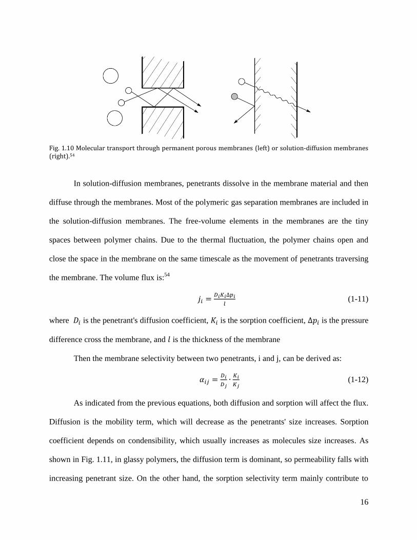
Fig. 1.10 Molecular transport through permanent porous membranes (left) or solution-diffusion
membranes (right).54
....................................................................................................... 16
Fig. 1.11 Permeability for rubbery and glassy polymers vs. gas molecular volume.55
................ 17
Fig. 1.12 Porous membranes’ key parameters: tortuosity (τ), porosity (ε), and average pore
diameter (d). 54
................................................................................................................ 19
Fig. 1.13 Transport mechanisms of porous membranes.54,56
........................................................ 19
Fig. 1.14 Illustration of the contributions of Poiseuille flow and Knudsen flow as a function of
r/λ.57
................................................................................................................................ 20
Fig. 1.15 Permeation of noncondensable and condensable gas mixtures through porous
membranes with Knudsen diffusion or molecular sieving.54
......................................... 21
xiii
Fig. 1.16 Blocking of hydrogen (noncondensable gas) by changing the amount of SO2
(condensable gas) with microporous membranes.60
....................................................... 22
Fig. 1.17 Schematic of gas molecules effusing through porous graphene membrane. ................. 23
Fig. 1.18 (a) top view of nitrogen passing through a porous graphene; (b) side view.61
.............. 24
Fig. 1.19 the 4N4H pore structure(carbon, cyan; hydrogen, grey; nitrogen, blue) has dimensions
of roughly 3.0*3.8Å2.9 .................................................................................................... 26
Fig. 1.20 Free energy profile of permeance for H2 and CO2 at 2atm as a function of the distance
between the centers of the gas molecule and the pore.62
................................................ 27
Fig. 1.21 Effects of pore functionalization and comparison with experimental results. (a) MD
results for pores without functionalization with existing experimental results. (b)
Comparison of MD results for selected pores with existing experimental results. (c-e)
schematic of the functinalized pores. Blue spheres, red spheres, and pink spheres
represent C atoms in graphene, H atoms, and C atoms in the functional groups.63
....... 28
Fig. 1.22 Schematic of zigzag stability (The up is the armchair case, and the bottom is the zigzag
case).66
............................................................................................................................ 29
Fig. 1.23 Edge reconfiguration.66
.................................................................................................. 30
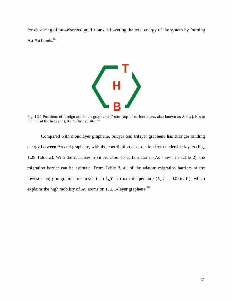
Fig. 1.24 Positions of foreign atoms on graphene: T site (top of carbon atom, also known as A
site), H site (center of the hexagon), B site (bridge site).67
............................................ 31
Fig. 1.25 Electron density images of monolayer and multiple layer graphene.69
......................... 32
Fig. 1.26 Au clusters on graphene with different substrates SiO2(left), Graphite(middle), h-
BN(right), after deposit 1Å of Au.70
............................................................................... 33
Fig. 1.27 (a) Charge density of an Au atom at different configuration edge. (b) Corresponded
binding energy to (a). (c) Migration of Au at zigzag edge. (d) Migration of Au at
armchair edge.71
.............................................................................................................. 34
Fig. 2.1 Scanning Electron Micrographs(SEM) showing doubly clamped beam NEMS device,
which is embedded in a nanofabricated UHF bridge circuit.73
...................................... 37
Fig. 2.2 Schematic of stress components. ..................................................................................... 38
Fig. 2.3 displacement vectors. ....................................................................................................... 40
Fig. 2.4 Deformation of infinitesimal strain components.76
......................................................... 40
Fig. 2.5 Schematic of bulged up membrane.77
.............................................................................. 42
Fig. 2.6 Geometrical reference diagram.77
.................................................................................... 43
Fig. 2.7 The motion of a damped oscillator on a time scale.80
..................................................... 46
Fig. 2.8 The schematic for the definition of quality factor in spectrum. ...................................... 46
Fig. 2.9 A circular membrane clamped at the edge.84
................................................................... 49
Fig. 2.10 First six mode-shapes with fixed boundary condition.84
............................................... 49
Fig. 2.11 Schematic of Michelson interferometer (left) and Fabry-Perot interferometer (right).90
........................................................................................................................................ 53

xiv
Fig. 2.12 (a) Schematic of the system set up; (b)Tested system.91
............................................... 55
Fig. 2.13 Frequency versus time for various gases with a pressure of 100 torr introduced into the
vacuum chamber. Inset: data from the same device with 80torr pressure.50
.................. 56
Fig. 3.1 Schematic of ALD using self-limiting surface chemistry and an AB binary reaction
sequence.95
...................................................................................................................... 60
Fig. 3.2 The materials grown by ALD.96
...................................................................................... 60
Fig. 3.3 Chemisorption mechanisms for ALD.97
.......................................................................... 62
Fig. 3.4 Schematic illustration of growth mode: (a) 2D growth, (b) island growth, and (c) random
deposition, where n is the cycle of growth.97
................................................................. 63
Fig. 3.5 GPC of TMA/H2O vs temperature.103,107-113
................................................................... 64
Fig. 3.6 (a) Schematic of NO2/TMA functionalization mechanism. NO2 is adsorbed on the CNT
surface, followed by TMA.139
(b) Illumination of oxide deposition process on graphene.
NO2/TMA pretreatment is followed by H2O/TMA growth.140
...................................... 66
Fig. 3.7 FESEM images of the residual impression remaining after indentation to (a) Al2O3, and
(b) SiO2 coatings on Si.141
.............................................................................................. 68
Fig. 3.8 load vs. depth for 500nm thick Al2O3 film on Si.141
........................................................ 68
Fig. 3.9 Stress results for 100nm Al2O3 deposited on Si.141
......................................................... 69
Fig. 3.10 (a) Bulge test results; (b) AFM-based nanobeam deflection measurements.143
............ 70
Fig. 3.11 Fabrication sequence of nanomechanical cantilevers devices and experimental
schematic for measuring the NEMS resonators.145
........................................................ 71
Fig. 4.1 Maximum deflection vs time before etching (a) Maximum deflection vs time for pristine
graphene with gold, formed porous graphene membrane in section 4.5&4.6; (insets):
optical image of monolayer graphene flake; (b) Maximum deflection vs time for pristine
graphene, which was before etching for membrane in section 4.7&4.8 (inlay): optical
image of monolayer graphene flake. .............................................................................. 75
Fig. 4.2 AFM amplitude images showing the movement of gold nanoparticles on a suspended
graphene membrane. ....................................................................................................... 79
Fig. 4.3 (a-c) Schematic of the gold nanoparticles (yellow solid circles) blocking and unblocking
the pore on the monolayer graphene membrane; (d-f) AFM height images capturing the
deflection change in (a-c). .............................................................................................. 80
Fig. 4.4 Deflection vs. position through the center of the membrane in Fig. 4.3 (d-f). ................ 80
Fig. 4.5 Maximum deflection vs. time for the dramatic leak rate change. The solid red line is a fit
to the data before switching using the membrane mechanics model. ............................ 81
Fig. 4.6 Maximum deflection of the graphene membrane before focusing a laser beam at the
center of the membrane. Different colors represent different charging pressures. The
charging pressure is from 200 kPa to 700 kPa to 200 kPa, in 100 kPa increments; (inset)
AFM amplitude images of the graphene membrane corresponding to the state of the
graphene membrane for the measurements. ................................................................... 83
xv
Fig. 4.7 Maximum deflection of the graphene membrane after focusing a laser beam at the center
of the membrane. Different colors represent different charging pressures. The charging
pressure is from 200 kPa to 850 kPa, in 50 kPa, 100 kPa, or 150 kPa increments. (inset)
AFM amplitude images of the graphene membrane corresponding to the state of the
graphene membrane for the measurements. ................................................................... 83
Fig. 4.8 (a) Leak rate dn/dt vs. pressure difference Δp for Fig. 4.6-shown in red and Fig. 4.7 –
shown in black; (b) Histogram of the permeance from (data in (a) –red) and (data in (b)-
black). ............................................................................................................................. 84
Fig. 4.9 Histogram of the permeance from (data in gray) to (data in magenta) by laser induced
heating again. .................................................................................................................. 85
Fig. 4.10 Leak rate dn/dt vs. pressure difference Δp for He gas (inset) Maximum deflection vs.
time for He gas. .............................................................................................................. 88
Fig. 4.11 Histogram of permeance for the noble gases, Ar, Ne, and He. ..................................... 88
Fig. 4.12 Permeance vs. kinetic diameter for all of the measured gases before (blue) and after
(black) etching. ............................................................................................................... 89
Fig. 4.13 Transmission coefficient vs. kinetic diameter for He, Ne, H2, and Ar. (inset)
Transmission coefficient vs. kinetic diameter for He, Ne, H2, N2O, CO2, and Ar. ........ 89
Fig. 4.14 Maximum Deflection vs time of multiple gases for porous monolayer graphene
membrane in Fig. 4.12&4.13. ......................................................................................... 90
Fig. 4.15 Stochastic switching of the leak rate through porous monolayer graphene without gold
nanoparticles (a) Permeance (black circles) and fit (red line) vs. time for all the Ne data.
Bottom axis, observable time, corresponds to the 800 minutes of measurements taken
over five days after repeated pressurization. Each measurement is separated by a dashed
line. (b) Single experimental run within (a) matching highlighted time range. Left axis,
blue squares - Maximum deflection versus time for Neon. Right axis– permeance vs.
time calculated from the change in deflection vs. time in. (c) Histogram of the
permeance for all the data in (a). .................................................................................... 91
Fig. 4.16 Atom Rearrangement at pore mouth. (a) Representation of a simple model pore
rearrangement. (b) Estimation of barrier energy for two pores depicted in (a) and the
expected ratio of permeance between the two. ............................................................... 94
Fig. 5.1 (a) Schematic of a graphene membrane before atomic layer deposition (ALD). (b) (upper)
Optical image of an exfoliated graphene flake with 7 cycles of alumina ALD. (lower)
side view schematic of this graphene/ALD composite. (c) Optical image of a pure
alumina film after graphene is etched away. (lower) side view schematic of this pure
ALD film. ....................................................................................................................... 99
Fig. 5.2 Bright-field TEM image of a cross-section of supported alumina ALD film on 5-layer
graphene supported on silicon oxide. The amorphous alumina layer is 2.8 ± 0.3 nm
thick. ............................................................................................................................. 100
Fig. 5.3 (a) Raman spectrum for one of the graphene/ALD composite films in Fig. 3.1b. (b) A
representative Raman spectrum on one of the pure alumina ALD films in Fig. 3.1C. 100
xvi
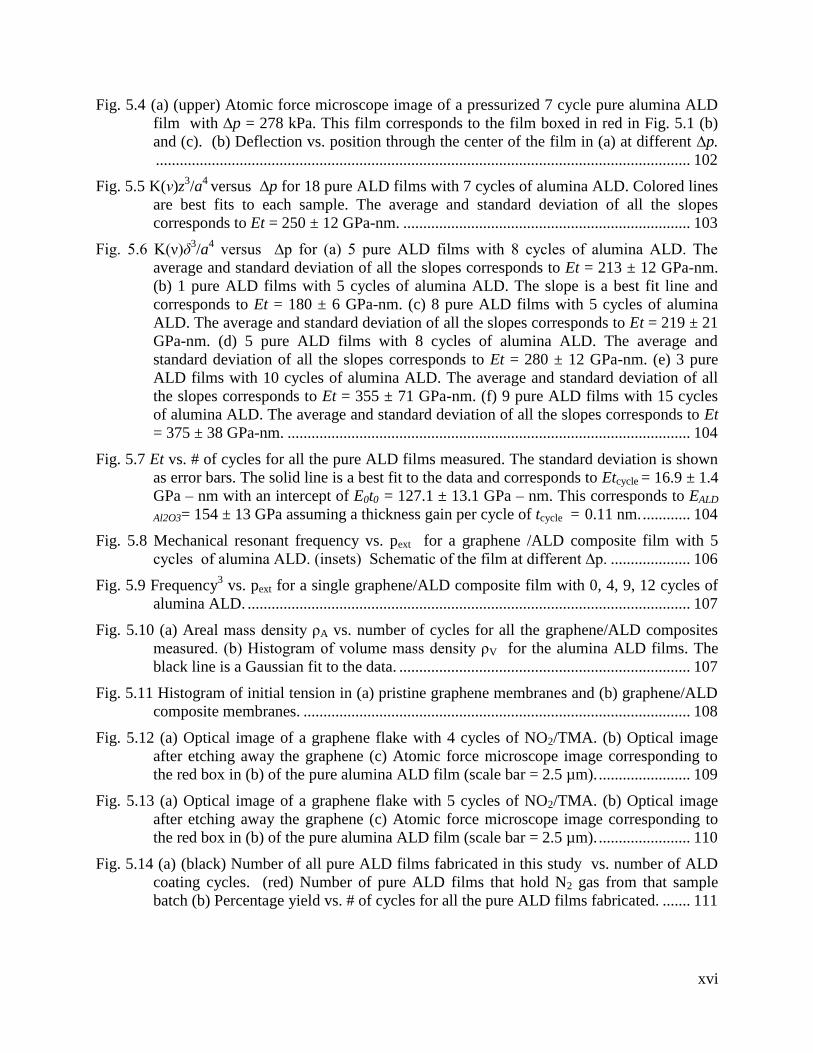
Fig. 5.4 (a) (upper) Atomic force microscope image of a pressurized 7 cycle pure alumina ALD
film with ∆p = 278 kPa. This film corresponds to the film boxed in red in Fig. 5.1 (b)
and (c). (b) Deflection vs. position through the center of the film in (a) at different ∆p.
...................................................................................................................................... 102
Fig. 5.5 K(ν)z3/a
4 versus ∆p for 18 pure ALD films with 7 cycles of alumina ALD. Colored lines
are best fits to each sample. The average and standard deviation of all the slopes
corresponds to Et = 250 ± 12 GPa-nm. ........................................................................ 103
Fig. 5.6 K(ν)δ3/a
4 versus ∆p for (a) 5 pure ALD films with 8 cycles of alumina ALD. The
average and standard deviation of all the slopes corresponds to Et = 213 ± 12 GPa-nm.
(b) 1 pure ALD films with 5 cycles of alumina ALD. The slope is a best fit line and
corresponds to Et = 180 ± 6 GPa-nm. (c) 8 pure ALD films with 5 cycles of alumina
ALD. The average and standard deviation of all the slopes corresponds to Et = 219 ± 21
GPa-nm. (d) 5 pure ALD films with 8 cycles of alumina ALD. The average and
standard deviation of all the slopes corresponds to Et = 280 ± 12 GPa-nm. (e) 3 pure
ALD films with 10 cycles of alumina ALD. The average and standard deviation of all
the slopes corresponds to Et = 355 ± 71 GPa-nm. (f) 9 pure ALD films with 15 cycles
of alumina ALD. The average and standard deviation of all the slopes corresponds to Et
= 375 ± 38 GPa-nm. ..................................................................................................... 104
Fig. 5.7 Et vs. # of cycles for all the pure ALD films measured. The standard deviation is shown
as error bars. The solid line is a best fit to the data and corresponds to Etcycle = 16.9 ± 1.4
GPa – nm with an intercept of E0t0 = 127.1 ± 13.1 GPa – nm. This corresponds to EALD
Al2O3= 154 ± 13 GPa assuming a thickness gain per cycle of tcycle = 0.11 nm. ............ 104
Fig. 5.8 Mechanical resonant frequency vs. pext for a graphene /ALD composite film with 5
cycles of alumina ALD. (insets) Schematic of the film at different ∆p. .................... 106
Fig. 5.9 Frequency3 vs. pext for a single graphene/ALD composite film with 0, 4, 9, 12 cycles of
alumina ALD. ............................................................................................................... 107
Fig. 5.10 (a) Areal mass density ρA vs. number of cycles for all the graphene/ALD composites
measured. (b) Histogram of volume mass density ρV for the alumina ALD films. The
black line is a Gaussian fit to the data. ......................................................................... 107
Fig. 5.11 Histogram of initial tension in (a) pristine graphene membranes and (b) graphene/ALD
composite membranes. ................................................................................................. 108
Fig. 5.12 (a) Optical image of a graphene flake with 4 cycles of NO2/TMA. (b) Optical image
after etching away the graphene (c) Atomic force microscope image corresponding to
the red box in (b) of the pure alumina ALD film (scale bar = 2.5 µm). ....................... 109
Fig. 5.13 (a) Optical image of a graphene flake with 5 cycles of NO2/TMA. (b) Optical image
after etching away the graphene (c) Atomic force microscope image corresponding to
the red box in (b) of the pure alumina ALD film (scale bar = 2.5 µm). ....................... 110
Fig. 5.14 (a) (black) Number of all pure ALD films fabricated in this study vs. number of ALD
coating cycles. (red) Number of pure ALD films that hold N2 gas from that sample
batch (b) Percentage yield vs. # of cycles for all the pure ALD films fabricated. ....... 111

1
Chapter 1 Introduction
1.1 Introduction
Two dimensional materials were forecast to be unstable, due to the rapid drop of melting
temperature of thin films.1-5
Though people have sought two dimensional materials for decades,
there was a lack of success until Geim and Noveselov first isolated graphene (purely two
dimensional crystal) from graphite at 2004.6 For graphite, there are strong covalent bonds in the
plane, and weak van der Waals forces, holding these sheets together. This makes graphite easy to
be shaved to form single atomic sheets of graphite or graphene. Graphene has superior properties,
including electrical, mechanical, and thermal properties. Our group is more interested in the
mechanical properties. Following are some of the mechanical properties, which are related to my
research. James Hone’s group used AFM nanoindentation to measure graphene’s breaking stress
of 130GPa, which is 100 times stronger than structural steel, and its Young’s modulus is ~1
TPa.7 Scott Bunch used a bulge test to detect that graphene is impermeable to standard gases.
8
This tells us that we may introduce customized nanopores into pristine graphene for separating
gases/ions or DNA sequencing.
For our research, graphene with pores is an ideal membrane material for gas separation. It
is atomically thin which means that flux is maximized. Its high breaking strength makes it
possible to bear high pressure difference for a long time, and pristine graphene is impermeable to
standard gases, which gives us the chance to create customized pores to separate our target gases.
From simulation results at Oak Ridge National Lab, the selectivity for H2/CH4 was predicted to
be extremely high for porous graphene.9
2
1.2 Outline
This thesis presents some of the first experiments on the gas separation properties of
porous graphene, the gas transport through single sub-nm pores in graphene, and the mechanical
properties of ultrathin Al2O3 ALD films. Chapter 1-3 give an overview of the basic concepts,
which are related to the experimental results presented later in this thesis. Chapter 4 contains the
experimental results for molecular sieving from porous graphene. Chapter 5 shows the first
experimental results of testing the interaction of gas molecules with single pores in graphene.
Chapter 6 is the first step to realizing gas separation from ultrathin Al2O3 ALD films. We studied
the production methods, as well as the mechanical properties for the films to pave the way for
ultrathin ALD films for gas separation.
1.3 Primary Accomplishments
By now, the research has been published in three journal articles and two conference
presentations.
Selected Peer Reviewed Journal Articles:
L. Wang, L. W. Drahushuk, S. P. Koenig, X. Liu, J. Pellegrino, M. S. Strano, J. S. Bunch.
“Single Nanopore Molecular Valves in Graphene for Controlling Gas Phase Transport”.
(Submitted)
S. P. Koenig, L. Wang, J. Pellegrino, J. S. Bunch. “Selective Molecular Sieving through
Porous Graphene”. Nature Nanotechnology, 7, 728-732, 2012
L. Wang, J. J. Travis, A. S. Cavanagh, X. Liu, S. P. Koenig, P. Y. Huang, S. M. George, J.
S. Bunch. “Ultrathin Oxide Films by Atomic Layer Deposition on Graphene” Nano Letters,

3
12(7), 3706-3710, 2012
Selected Conference Presentations:
American Physics Society(APS), March 2014, Presentation
Material Research Society(MRS), Fall 2012, Poster
Technical Contributions:
Built and set up the optics for Nano-Electrical-Mechanical-Systems (NEMS) mechanical
resonators drive and detection with the help of Steven Koenig and following Harold
Craighead group’s design. Aligned the optics and updated the components, which achieved
and optimized the resonance signal. Was in charge of the resonance measurements for the lab.
Maintained and repaired the atomic force microscope.
Assembled several pressure chambers for bulge test measurements.
1.4 Graphene and Other Two-Dimensional Materials
A wonderful material with many advantages, graphene is a rising star in science. It is a
single atomic layer of sp2-bonded carbon atoms arranged in a close-packed honeycomb lattice.
Many of graphene’s unique properties can be derived from its chemical structure10,11
, which is
presented in Fig. 1.1.
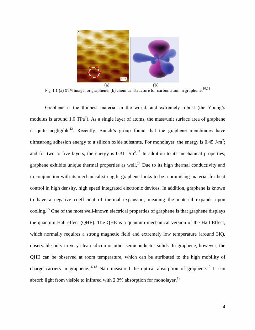
4
(a) (b)
Fig. 1.1 (a) STM image for graphene; (b) chemical structure for carbon atom in graphene.10,11
Graphene is the thinnest material in the world, and extremely robust (the Young’s
modulus is around 1.0 TPa7). As a single layer of atoms, the mass/unit surface area of graphene
is quite negligible12
. Recently, Bunch’s group found that the graphene membranes have
ultrastrong adhesion energy to a silicon oxide substrate. For monolayer, the energy is 0.45 J/m2;
and for two to five layers, the energy is 0.31 J/m2.13
In addition to its mechanical properties,
graphene exhibits unique thermal properties as well.14
Due to its high thermal conductivity and
in conjunction with its mechanical strength, graphene looks to be a promising material for heat
control in high density, high speed integrated electronic devices. In addition, graphene is known
to have a negative coefficient of thermal expansion, meaning the material expands upon
cooling.15
One of the most well-known electrical properties of graphene is that graphene displays
the quantum Hall effect (QHE). The QHE is a quantum-mechanical version of the Hall Effect,
which normally requires a strong magnetic field and extremely low temperature (around 3K),
observable only in very clean silicon or other semiconductor solids. In graphene, however, the
QHE can be observed at room temperature, which can be attributed to the high mobility of
charge carriers in graphene.16-18
Nair measured the optical absorption of graphene.19
It can
absorb light from visible to infrared with 2.3% absorption for monolayer.19

5
There are three primary ways to make graphene. Firstly, the easiest and traditional way is
mechanical exfoliation. Graphene sheets can be stacked to form graphite, however each layer is
only held to another by weak van der Waals forces. Because of the strong bonding within a sheet
of graphene and weak bonding between sheets, one is able to produce graphene by cleaving apart
sheets of graphene from graphite using scotch tape.6 Secondly, graphene can be created from
epitaxial growth.20,21
After heating up SiC in argon, Si will sublimate. The residue carbon atoms
will assemble into graphene layers. But one drawback of SiC is the expensive price of the
material. Thirdly, the most common used method growth method is chemical vapor deposition
(CVD). They are two widely used catalysts, nickel22
and copper.23
Since the layers and qualities
of graphene are hard to be controlled for nickel foil, most of the labs use copper for growth. The
graphene growth on copper is a surface-catalyzed process, wherein surface decomposition of the
precursor leaves carbon atoms that assemble into the 2-D graphene without carbon intercalation
into the metal.23
So the graphene growth on Cu is self-limited monolayer growth. As shown in
Fig. 1.2, Ruoff’s group reported graphene flakes as big as millimeters in diameter.24
Fig. 1.2 large graphene domain.
24
After graphene was discovered, other layered materials were also studied.25
Transition
metal oxides and transition metal dichalcogenides have layered structures,26
which makes them
major 2D materials beyond graphene for study. For the electrical properties, NbS2, NbSe2, and
6
TaSe2 are superconductors;26
NiTe2 and VSe2 are semi-metals,26
WS2, WSe2, MoS2, MoSe2,
MoTe2, TaS2, RhTe2, PdTe2 are semiconductors,26
h-BN, and HfS2 are insulators.26
For instance,
bulk MoS2 has an indirect band gap, while the monolayer one has a direct band gap.27,28
Decreasing the layer number N in MoS2 leads to the gain in the indirect gap, with the direct gap
almost unchanged. The indirect-direct-gap crossover is achieved with monolayer thickness.28
Several methods can lead you to a single layer from layered materials, i.e. mechanical
exfoliation,29
laser ablation,30
liquid phase exfoliation,31
and synthesis by thin film techniques.32
One application for the layered materials is atomically thin heterostructures.25
One can stack
conductive, semi-conductive, insulating materials with atomic precision, fine-tuning the
performance of the resulting material.33
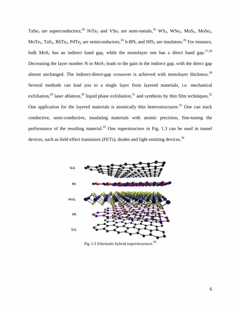
One superstructure in Fig. 1.3 can be used in tunnel
devices, such as field effect transistors (FETs), diodes and light emitting devices.34
Fig. 1.3 Schematic hybrid superstructure.
34
7
1.5 Nanopores
Pristine graphene is impermeable8 to any standard gases or other molecules, which makes
graphene an ideal starting material for nanopore applications. By tuning the size of nanopores,
one can achieve DNA sequencing (few nanometers), ion separation (few angstroms), or gas
separation (few angstroms).
To get a thorough understanding of nanopores through graphene, we may need to review
the history of nanopores. DNA sequencing is one of the biggest and most important applications
for nanopores since it is a label-free, amplification-free, single-molecule approach which
involves low reagent volumes and low cost.35
The mainstream method is ion-current blockade:
Since the DNA is a charged molecule, the electric field across the nanopore will drive DNA
through it. Once DNA goes through the pore, it will partially block the path of ions, which leads
to a drop in the ionic current (as shown in Fig. 1.4).36
In the case of a cylindrical solid-state
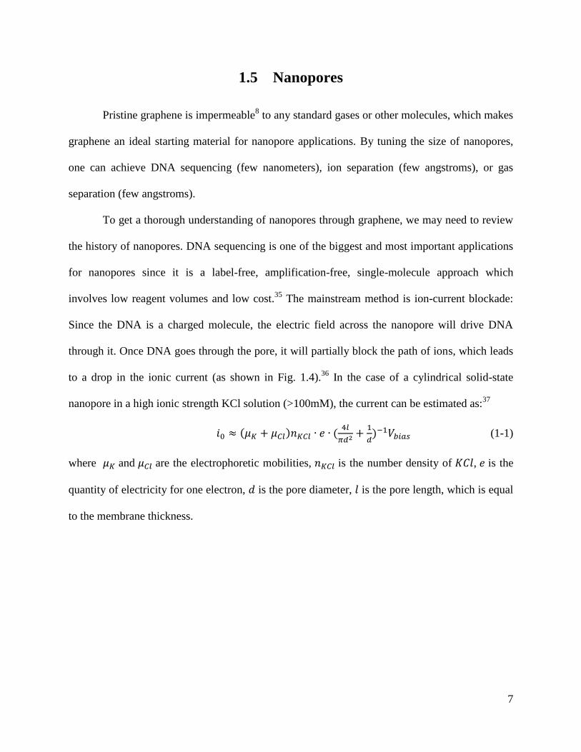
nanopore in a high ionic strength KCl solution (>100mM), the current can be estimated as:37
(1-1)
where and are the electrophoretic mobilities, is the number density of , is the
quantity of electricity for one electron, is the pore diameter, is the pore length, which is equal
to the membrane thickness.

8
Fig. 1.4 (a) Schematic of DNA passing the nanopore, with corresponded ionic current; (b) Four parameters in translocation process: the blockade duration tdwell, the time between translocation events τ, the amplitude of blockade current, the capture rate.36
In the 1990s, biological pore α-haemolysin was accomplished for DNA
sensing/sequencing.38
Though α-haemolysin is dominant as a biological nanopore, other more
efficient biological nanopores are emerging, i. e. octameric protein channel MspA.39
Biological
pores have proved to be useful for translocation experiments, but they also have some limitations:
fixed sizes, lack of stability, and are ultra-sensitive to experimental conditions (pH, temperature,

9
mechanical stress, and salt concentration).35,38
Interest in solid-state nanopores has been
increasing rapidly these years, due to their high stability, controllability of pore size, versatile-
design ability.35,38
The fabrication of solid-state nanopores includes thin membrane fabrication,
and nanopore probing. SiNx has traditionally been the nanopore membrane material, due to its
high chemical stability and low mechanical stress.35
From Fig. 1.5, thin SiNx layer is deposited to
both sides of bare Si. Using photolithography, followed by reactive ion etching to etch away
designated pattern for the bottom SiNx. Then the anisotropic wet etching is present to etch
through the Si to form the suspended SiNx membrane on top. The last step is poking hole on the
membrane, through ion beam sculpting or other methods.36
The nanopore probing is the key
process for solid-state nanopores. Different methods can be chosen for different membrane
materials, i.e. SiN, SiO2, SiC, Al2O3, or graphene (Fig. 1.6).
Compared with other materials, graphene has huge advantages for nanopore applications.
From the ionic current equation, we can see that the thinner the membrane, the larger the current.
But the fabrication of robust, ultrathin membranes from traditional materials is a challenge.
Golovchenko’s group successfully made nanopores on graphene for DNA sensing.40
As shown
in Fig. 1.7, individual double-stranded DNA (dsDNA) molecules were detected using 8nm
nanopores in suspended chemical vapor deposition (CVD) graphene by a focused electron beam.
They found that the ionic conductance of the nanopore was proportional to the pore diameter
instead of pore area.40
This agrees with theory for an effective membrane thickness of almost
zero, whose dominant resistance is the access resistance, which is inversely proportional to the
pore diameter.41

10
Nanopores are widely used as biosensors. Besides the potential for DNA
sensing/sequencing, nanopores have some immediate applications, including medical diagnostics,
MicroRNA expression profiling, epigenetic analysis, genetic analysis, and genomic profiling.35
Fig. 1.5 Schematic of the fabrication for a membrane and nanopores.36

11
Fig. 1.6 Various images of solid-state nanopores. (a) 1.8nm nanopore in SiNx from Ar-ion beam sculption.42 (b) 2nm nanopore in SiO2, using tightly focused electron beam followed by high-intensity wide-field TEM illumination.43 (c) TEM image of sub-10 nm nanopore on graphene fabricated by transmission electron beam ablation lithography.44 (d) 3 nm pore poked with a Ga focused ion beam in SiC membrane.45 (e) 4nm nanopore fabricated from He ion microscope in a SiNx membrane.46 (f) 18nm nanopore from electrochemically deposition with Pt.47 (g) 30nm nanopore from local oxide deposition with ion-beam deposition.48 (h) 2nm nanopore from local oxide deposition with electron-beam induced deposition.49
Fig. 1.7 Top left: Schematic of the nanopore on the suspended graphene film; Top right: TEM image of the 8nm nanopore; Bottom: graph of event blockage vs. event duration showing the ability to distinguish the folded DNA(inset left) and unfolded one (inset right).40
12
1.5 Gas Transport Mechanisms through Permselective
Membranes
In the previous section, we introduced the concept of nanopores, especially the few
nanometer diameter nanopores in graphene for DNA sensing. This chapter, we will focus on
membranes, which contain pores (or free volume) for gas separation. Especially, we will
highlight nanopores with few angstrom diameters on graphene, which can be used for molecular
sieving/effusion gas separation. To the best to our knowledge, no group has experimentally
achieved angstrom-sized nanopores for gas separation in graphene prior to our work.50
But
theoretical and simulation work previously done guided our research.
To understand gas separation it is necessary to understand the fundamentals of gas
transport. Gas kinetic theory makes a bridge between the macroscopic properties and their
microscopic constituents. Though the size of a gas molecule is in the angstrom range, they still
obey the classical mechanical laws of matter in most situations. The kinetic theory is based on
dynamics and statistics. Due to the dilute density of gases compared with liquids or solids, the
gas molecules move about freely and are separated by large distance compared with their
dimensions. Like classical particles, they move in straight lines until a collision occurs. After
they separate, they will move off with different velocities. Velocity and position are two
important parameters for the molecules' movement. Phase space is a two dimensional space
which specifies the location and velocity of the particle.
The Maxwell-Boltzmann distribution is the distribution of molecular velocities under
equilibrium conditions.

13
(1-2)
where
,
. , , and are the molecular mass, Boltzmann’s constant and the
temperature, respectively.
The parameter is directly related to the average kinetic energy of molecules.
(1-3)
After putting in all the values for the parameters, the speed distribution of molecules
under equilibrium conditions is (Fig. 1.8):
(1-4)
Fig. 1.8 Maxwell-Boltzmann distribution.51
where the scale parameter
.
The mean value of the velocity is:52
14
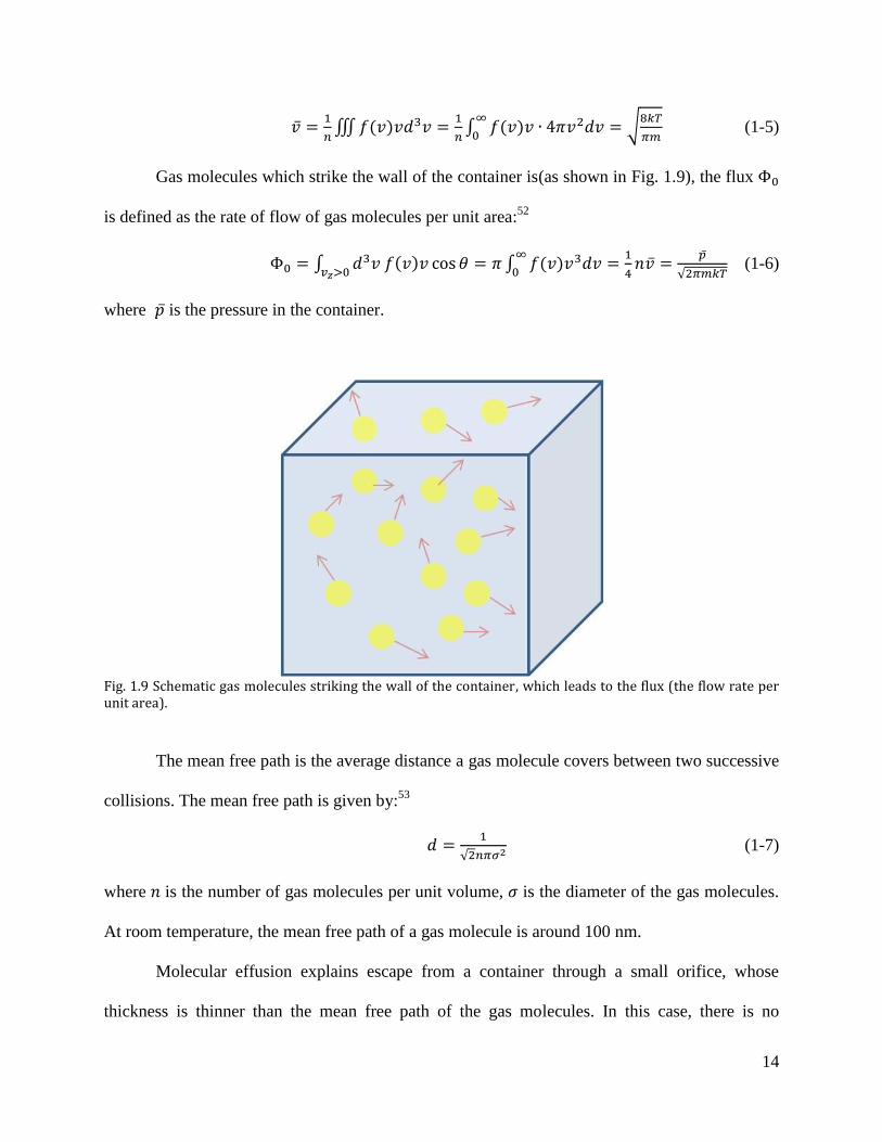
(1-5)
Gas molecules which strike the wall of the container is(as shown in Fig. 1.9), the flux
is defined as the rate of flow of gas molecules per unit area:52
(1-6)
where is the pressure in the container.
Fig. 1.9 Schematic gas molecules striking the wall of the container, which leads to the flux (the flow rate per unit area).
The mean free path is the average distance a gas molecule covers between two successive
collisions. The mean free path is given by:53
(1-7)
where is the number of gas molecules per unit volume, is the diameter of the gas molecules.
At room temperature, the mean free path of a gas molecule is around 100 nm.
Molecular effusion explains escape from a container through a small orifice, whose
thickness is thinner than the mean free path of the gas molecules. In this case, there is no
15
collision of the gas molecules to the walls of the pore, and the gas molecules will either be
rejected by the wall, or directly go across the pore.53
Based on the flux of gas molecules striking
the wall, the number of molecules escaping from the container is:
(1-8)
where is the area of the hole, is the mass weight, and is the gas constant. This is the
classical effusion model, which will be used in the follow sections. To step ahead, the classical
effusion describes molecules leaving box through a hole to vacuum; the number of residual
molecules in the box at time t is:
(1-9)
where is the number of molecules at t=0, is the pore area, is the volume of the box. The
time constant is the time for the system to lose (1-1/e) of its total number of molecules, which
means the decay time constant in this system is:
(1-10)
Based on the theory of gas transport, membranes can be used to control the rate of
permeations of different species to achieve gas separation. Normally, membranes are divided
into two groups: microporous membranes and dense solution-diffusion membranes (as shown in
Fig. 1.10).54
16
Fig. 1.10 Molecular transport through permanent porous membranes (left) or solution-diffusion membranes (right).54
In solution-diffusion membranes, penetrants dissolve in the membrane material and then
diffuse through the membranes. Most of the polymeric gas separation membranes are included in
the solution-diffusion membranes. The free-volume elements in the membranes are the tiny
spaces between polymer chains. Due to the thermal fluctuation, the polymer chains open and
close the space in the membrane on the same timescale as the movement of penetrants traversing
the membrane. The volume flux is:54
(1-11)
where is the penetrant's diffusion coefficient, is the sorption coefficient, is the pressure
difference cross the membrane, and is the thickness of the membrane
Then the membrane selectivity between two penetrants, i and j, can be derived as:
(1-12)
As indicated from the previous equations, both diffusion and sorption will affect the flux.
Diffusion is the mobility term, which will decrease as the penetrants' size increases. Sorption
coefficient depends on condensibility, which usually increases as molecules size increases. As
shown in Fig. 1.11, in glassy polymers, the diffusion term is dominant, so permeability falls with
increasing penetrant size. On the other hand, the sorption selectivity term mainly contribute to

17
the permeance in rubbery polymers. As a result, permeability increases as increasing the
molecule's size in rubbery polymers. In application, glassy polymers can be used to permeate air
gases (i. e. nitrogen) from organic vapors, while rubbery polymers permeate the organic
vapors.55
Fig. 1.11 Permeability for rubbery and glassy polymers vs. gas molecular volume.55
In pore-flow membranes, the penetrants are transported through tiny permanent pores by
pressure-driven flow. The key parameters in porous membranes are tortuosity, porosity, and
average pore diameter as shown in Fig. 1.12. Differing in pore sizes, porous membranes can
follow different mechanisms (Fig. 1.13). If the pore are relatively large (>1μm), gas permeate the
membrane by convective flow, wherein no separation occurs. If the pores are relatively small
(similar to the mean free path of the gas molecules), the diffusion through pores follow Knudsen

18
diffusion. The contributions combine convective flow and Knudsen diffusion is shown in Fig.
1.14. If the pores are extremely small, molecular sieving transport dominates the permeance.
For convective (Poiseuille) flow, the permeation flux is given by:54
(1-13)
where is the pore radius, is the porosity of the membrane, is the tortuosity, is the thickness
of the membrane, , is the pressure on two sides of the membrane, is the viscosity of the
gas, is the ideal gas constant, and is the temperature. From the permeance equation of
convective flow, we can see that there is no selectivity for different gas species.
For Knudsen diffusion, the permeation is:54
(1-14)
where is the mass weight of the gas species. The Knudsen diffusion equation gives us
indication that the gas species can be separated by the molecular mass differences.

19
Fig. 1.12 Porous membranes’ key parameters: tortuosity (τ), porosity (ε), and average pore diameter (d). 54
Fig. 1.13 Transport mechanisms of porous membranes.54,56
20
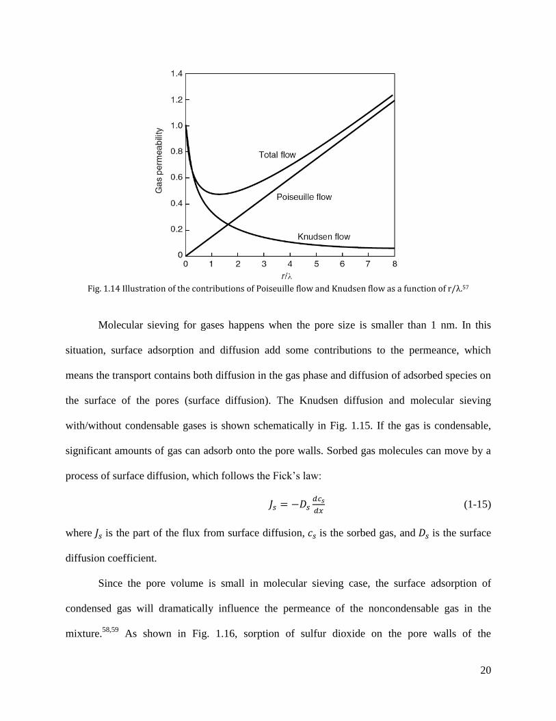
Fig. 1.14 Illustration of the contributions of Poiseuille flow and Knudsen flow as a function of r/λ.57
Molecular sieving for gases happens when the pore size is smaller than 1 nm. In this
situation, surface adsorption and diffusion add some contributions to the permeance, which
means the transport contains both diffusion in the gas phase and diffusion of adsorbed species on
the surface of the pores (surface diffusion). The Knudsen diffusion and molecular sieving
with/without condensable gases is shown schematically in Fig. 1.15. If the gas is condensable,
significant amounts of gas can adsorb onto the pore walls. Sorbed gas molecules can move by a
process of surface diffusion, which follows the Fick’s law:
(1-15)
where is the part of the flux from surface diffusion, is the sorbed gas, and is the surface
diffusion coefficient.
Since the pore volume is small in molecular sieving case, the surface adsorption of
condensed gas will dramatically influence the permeance of the noncondensable gas in the
mixture.58,59
As shown in Fig. 1.16, sorption of sulfur dioxide on the pore walls of the

21
microporous carbon membrane can restrict or even completely block the flow of hydrogen,
depending on the amount of SO2 sorbed.60
Fig. 1.15 Permeation of noncondensable and condensable gas mixtures through porous membranes with Knudsen diffusion or molecular sieving.54

22
Fig. 1.16 Blocking of hydrogen (noncondensable gas) by changing the amount of SO2 (condensable gas) with microporous membranes.60
The thinner the membrane, the larger the flux we can get. Using ultrathin films as the
selective barrier is always a target for the development of membranes. A single layer graphene
membrane is an ideal material for gas separation, due to its atomic thickness, ultra high strength,
and chemically inert nature. However, the conventional analysis of diffusive transport through a
membrane fails into the case of 2D atomically thin membranes.61
Following is the gas transport
mechanism for atomic thin porous graphene membranes. There are two potential pathways for
gas transport through porous single layer graphene: i.) effusion pathway; ii.) adsorbed phase
pathway.61
For the effusion pathway, the pores in graphene membranes have sub-nm diameter (Fig.
1.17). As the size of the pore is comparable to the size of gas molecules, the shape and size of
gas molecules cannot be ignored. This is because as the gas molecules are slightly off the center
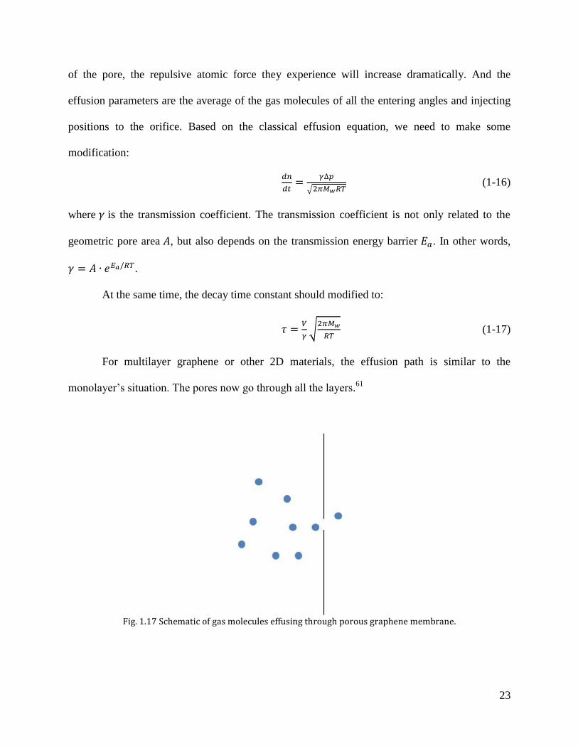
23
of the pore, the repulsive atomic force they experience will increase dramatically. And the
effusion parameters are the average of the gas molecules of all the entering angles and injecting
positions to the orifice. Based on the classical effusion equation, we need to make some
modification:
(1-16)
where is the transmission coefficient. The transmission coefficient is not only related to the
geometric pore area , but also depends on the transmission energy barrier . In other words,
.
At the same time, the decay time constant should modified to:
(1-17)
For multilayer graphene or other 2D materials, the effusion path is similar to the
monolayer’s situation. The pores now go through all the layers.61
Fig. 1.17 Schematic of gas molecules effusing through porous graphene membrane.

24
The adsorbed phase pathway contains five steps (Fig. 1.18).61
Firstly, a gas molecule
adsorbed to a site on the surface. Secondly, the molecule diffuses to an orifice and moves into a
potential well positioned in the space above the orifice. Thirdly, the molecule passes through the
pore to the other side of the graphene. Fourthly, the molecule disassociates from the area of the
pore onto the downstream surface of the graphene. Finally, the molecule desorbs from the
surface. The whole process is schematically described in Fig. 1.18. In step 2, the molecule must
both diffuse to the pore and overcome an activation barrier to position itself above the pore.61
The permeance of adsorbed phase pathway will saturate at some pressure, which means the leak
rate dn/dt vs. pressure difference Δp will not follow linear trend as Δp increases. This is one
method to distinguish adsorbed path way with the gas phase pathway, which gives the linear
relation between dn/dt and Δp.
Fig. 1.18 (a) top view of nitrogen passing through a porous graphene; (b) side view.
61

25
1.6 Pore Functionalization for Porous Graphene Membranes
For the transport of gas through graphene membranes, not only does the molecular mass,
kinetic diameter, and molecular adsorption matter, but also the pore functionalization can play a
key role.62,63
For the calculation of gas transport, molecular dynamics (MD) simulation is the
popular method. For MD simulation, each of the N molecules is treated as a point mass and
Newton’s equations are integrated to simulate their motion.64
Classical MD simulations have
small computational cost, which allow the simulation of large number of molecular trajectories.63
This method is accurate enough for the gases with enough observable passing-through events
within the simulation conditions and time frames. But for the gases with high barrier under
limited driving force, MD simulation does not give statistically sufficient results for the passing-
through events.
The free energy profile can be calculated in the simulations, and is a theoretical
representation of a single energetic pathway, which is along the reaction coordinate.65
Free
energy profile gives additional information for the gases, which overcomes the kinetic resolution
limitation of MD simulation.62
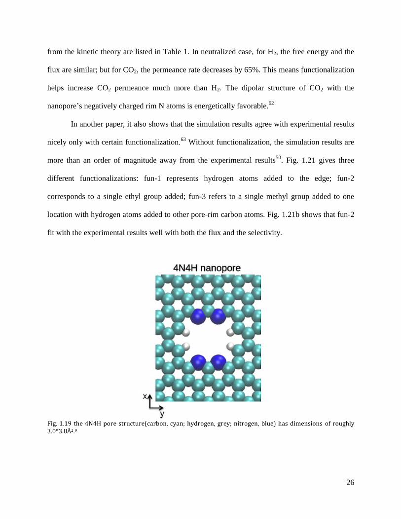
A theoretical and computational study showed that a 4N4H
nanopore (Fig. 1.19) with four dangling bonds saturated by hydrogen atoms and other four
dangling bonds saturated by nitrogen atoms.9 The 3.0 Å * 3.8 Å pore can distinguish five gases
(H2, CO2, Ar, N2, and CH4) into two groups based on their sizes: a fast permeation rate for H2,
CO2, and an extremely slow one for Ar, N2 and CH4, which agrees with the experimental
results50
. In order to study the effect of the functionalization, one can manually include or
neutralize the charge to separate the functionality effect with the effect of geometrical pore size
for the same pore. For example, Fig. 1.20 gives the comparison of the free energy profiles for H2
and CO2 between the original porous graphene and the neutralized one. And the estimated fluxes
26
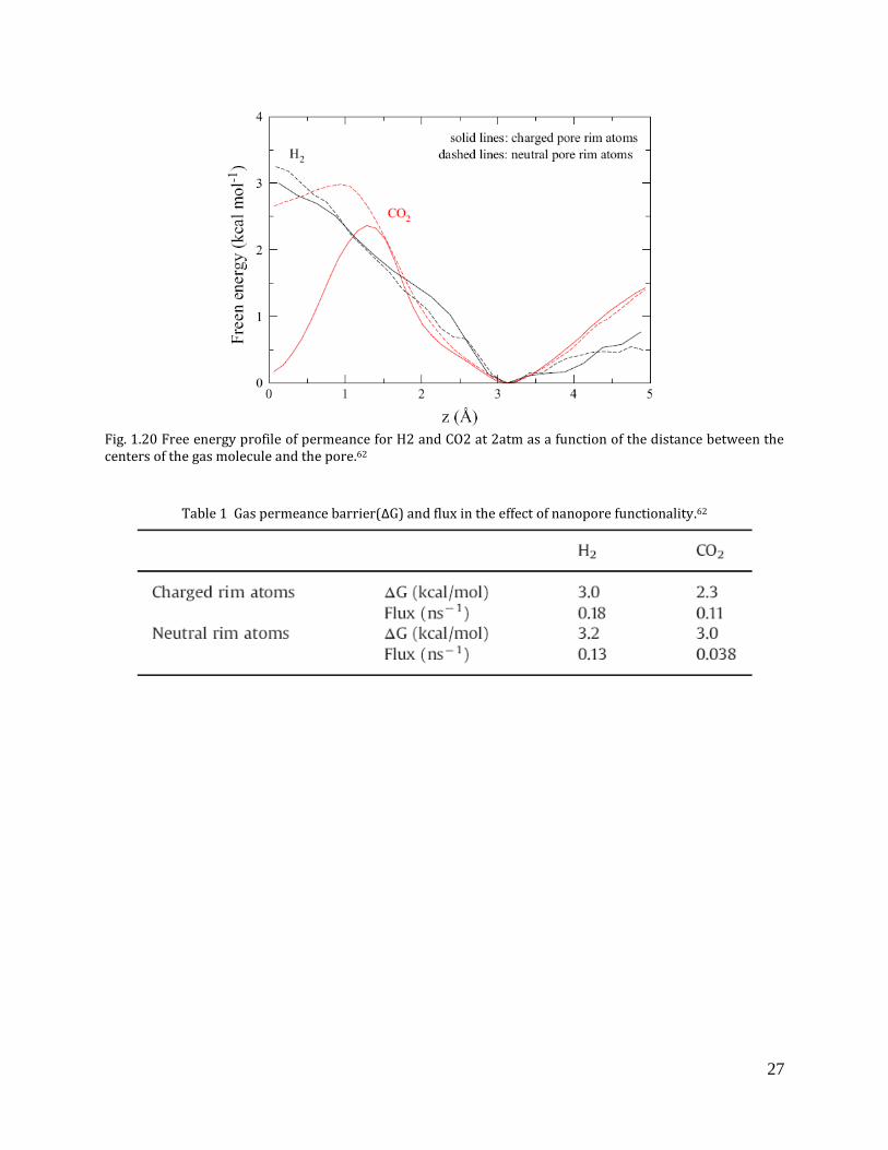
from the kinetic theory are listed in Table 1. In neutralized case, for H2, the free energy and the
flux are similar; but for CO2, the permeance rate decreases by 65%. This means functionalization
helps increase CO2 permeance much more than H2. The dipolar structure of CO2 with the
nanopore’s negatively charged rim N atoms is energetically favorable.62
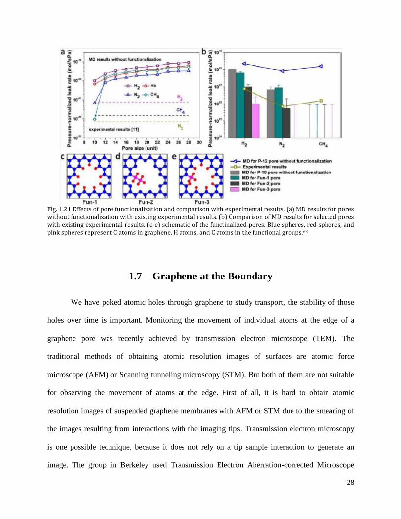
In another paper, it also shows that the simulation results agree with experimental results
nicely only with certain functionalization.63
Without functionalization, the simulation results are
more than an order of magnitude away from the experimental results50
. Fig. 1.21 gives three
different functionalizations: fun-1 represents hydrogen atoms added to the edge; fun-2
corresponds to a single ethyl group added; fun-3 refers to a single methyl group added to one
location with hydrogen atoms added to other pore-rim carbon atoms. Fig. 1.21b shows that fun-2
fit with the experimental results well with both the flux and the selectivity.
Fig. 1.19 the 4N4H pore structure(carbon, cyan; hydrogen, grey; nitrogen, blue) has dimensions of roughly 3.0*3.8Å2.9
27
Fig. 1.20 Free energy profile of permeance for H2 and CO2 at 2atm as a function of the distance between the centers of the gas molecule and the pore.62
Table 1 Gas permeance barrier(ΔG) and flux in the effect of nanopore functionality.62
28
Fig. 1.21 Effects of pore functionalization and comparison with experimental results. (a) MD results for pores without functionalization with existing experimental results. (b) Comparison of MD results for selected pores with existing experimental results. (c-e) schematic of the functinalized pores. Blue spheres, red spheres, and pink spheres represent C atoms in graphene, H atoms, and C atoms in the functional groups.63
1.7 Graphene at the Boundary
We have poked atomic holes through graphene to study transport, the stability of those
holes over time is important. Monitoring the movement of individual atoms at the edge of a
graphene pore was recently achieved by transmission electron microscope (TEM). The
traditional methods of obtaining atomic resolution images of surfaces are atomic force
microscope (AFM) or Scanning tunneling microscopy (STM). But both of them are not suitable
for observing the movement of atoms at the edge. First of all, it is hard to obtain atomic
resolution images of suspended graphene membranes with AFM or STM due to the smearing of
the images resulting from interactions with the imaging tips. Transmission electron microscopy
is one possible technique, because it does not rely on a tip sample interaction to generate an
image. The group in Berkeley used Transmission Electron Aberration-corrected Microscope
29
monochromated (TEAM0.5) to achieve sub-angstrom resolution with 80kV.66
The low voltage
will nearly prevent the damage of the edge from the electron beam itself. Each frame averages 1s
of exposure, which is dramatically faster than the AFM/STM. They demonstrated that the
dominant process in the dynamics of carbon atoms at the edge of the hole is the migration of
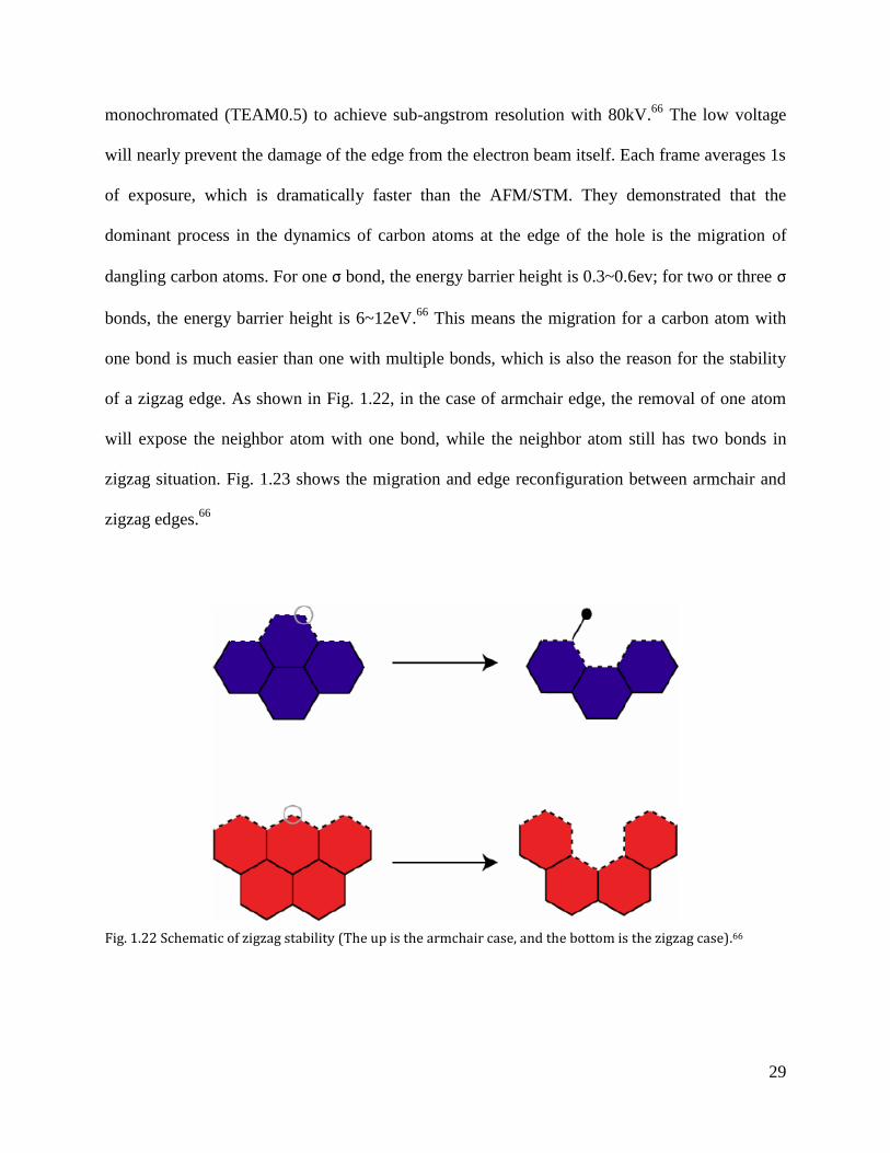
dangling carbon atoms. For one σ bond, the energy barrier height is 0.3~0.6ev; for two or three σ
bonds, the energy barrier height is 6~12eV.66
This means the migration for a carbon atom with
one bond is much easier than one with multiple bonds, which is also the reason for the stability
of a zigzag edge. As shown in Fig. 1.22, in the case of armchair edge, the removal of one atom
will expose the neighbor atom with one bond, while the neighbor atom still has two bonds in
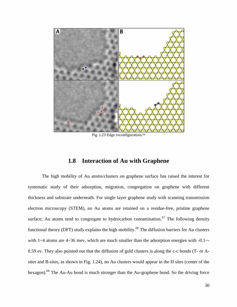
zigzag situation. Fig. 1.23 shows the migration and edge reconfiguration between armchair and
zigzag edges.66
Fig. 1.22 Schematic of zigzag stability (The up is the armchair case, and the bottom is the zigzag case).66
30
Fig. 1.23 Edge reconfiguration.66
1.8 Interaction of Au with Graphene
The high mobility of Au atoms/clusters on graphene surface has raised the interest for
systematic study of their adsorption, migration, congregation on graphene with different
thickness and substrate underneath. For single layer graphene study with scanning transmission
electron microscopy (STEM), no Au atoms are retained on a residue-free, pristine graphene
surface; Au atoms tend to congregate to hydrocarbon contamination.67
The following density
functional theory (DFT) study explains the high mobility.68
The diffusion barriers for Au clusters
with 1~4 atoms are 4~36 mev, which are much smaller than the adsorption energies with -0.1~-
0.59 ev. They also pointed out that the diffusion of gold clusters is along the c-c bonds (T- or A-
sites and B-sites, as shown in Fig. 1.24), no Au clusters would appear in the H sites (center of the
hexagon).68
The Au-Au bond is much stronger than the Au-graphene bond. So the driving force
31
for clustering of pre-adsorbed gold atoms is lowering the total energy of the system by forming
Au-Au bonds.68
Fig. 1.24 Positions of foreign atoms on graphene: T site (top of carbon atom, also known as A site), H site (center of the hexagon), B site (bridge site).67
Compared with monolayer graphene, bilayer and trilayer graphene has stronger binding
energy between Au and graphene, with the contribution of attraction from underside layers (Fig.
1.25 Table 2). With the distances from Au atom to carbon atoms (As shown in Table 2), the
migration barrier can be estimate. From Table 3, all of the adatom migration barriers of the
lowest energy migration are lower than at room temperature ( ), which
explains the high mobility of Au atoms on 1, 2, 3-layer graphene.69

32
Fig. 1.25 Electron density images of monolayer and multiple layer graphene.69
Table 2 Adatom binding energies, Au- carbon distances by ab initio DFT study.69
Table 3 Calculated migration barriers for Au on the lowest nergy migration pathways on pristine graphene by ab initio DFT.69

33
Substrates under the graphene will significantly slow down the Au atom diffusion on
graphene. The Au adatom diffusion constant for graphene on SiO2 is 50 times smaller than that
for hexagonal boron nitride supported graphene, and 800 times smaller than that for multilayer
graphite70
. The diffusion constant is inversely proportional to the diffusion energy barrier, which
means graphene on SiO2 has the largest diffusion energy barrier. As shown in Fig. 1.26, the size
of Au clusters on graphene with SiO2 is smaller than that on graphite or h-BN substrates with the
same evaporation condition, due to the strong diffusion energy barrier.70
Fig. 1.26 Au clusters on graphene with different substrates SiO2(left), Graphite(middle), h-BN(right), after deposit 1Å of Au.70
The Au atoms may not only interact with graphene surface, but also interact with the
graphene edge. The dangling bond at the edge of graphene makes a stronger binding energy
between Au atom and graphene, which results in a high migration barrier for Au to diffuse along
the edge. Fig. 1.27 gives that the binding energy of Au at the edge is from 3eV to 6eV, and the
energy barrier for diffusion on armchair edge is one order stronger than the barrier for zigzag
case.71
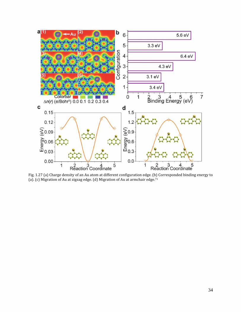
34
Fig. 1.27 (a) Charge density of an Au atom at different configuration edge. (b) Corresponded binding energy to (a). (c) Migration of Au at zigzag edge. (d) Migration of Au at armchair edge.71

35
1.9 Conclusions
Some fundamental concepts were introduced in this chapter to pave the way for
following chapters. Graphene is well studied 2D material, and introducing nanopores in graphene
has become a niche area. DNA translocation through few-nm nanopores on graphene was
achieved. Few-angstrom nanopores on graphene membrane are projected to be useful in gas
separations by theory and simulation. The pore functionalization may affect the permeance of the
graphene membranes. Moreover, the atoms movement at the boundary (pore mouth) may affect
the performance of the porous graphene membranes. In Chapter 4, we will introduce the first
experimental results, using porous graphene for the gas separation. In Chapter 5, we will talk
about the interaction between the gas molecules and the single pores. In the next chapter, we will
focus on the mechanical properties of NEMS.

36
Chapter 2 Nanomechanics
2.1 Introduction
Suspended graphene devices are part of the family of nanoelectromechanical systems
(NEMS). In this section, we will introduce the definition, advantages, challenges and significant
applications of NEMS.72
NEMS are made of mechanical elements and electronic circuits on the
nano scale. Electro-mechanical systems contain two parts: a mechanical element and transducer.
The mechanical element will change the input into the movement of the mechanical element. It
can be the deflection under the applied force, the change of the amplitude of oscillation, the
difference of the frequency of oscillation and so on. A transducer converts mechanical energy to
electrical or optical signals. Nano-electromechanical systems are mechanical elements and
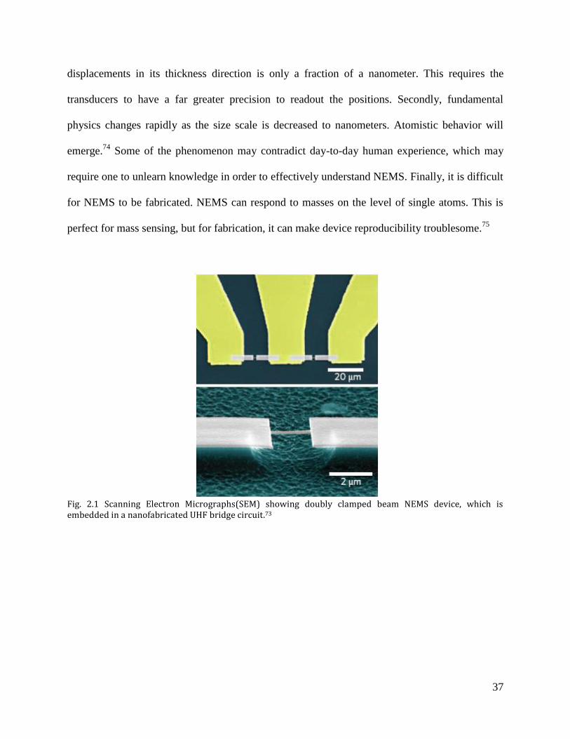
electronic circuits on the nano scale (Fig. 2.1).72
NEMS are ultralow-power devices. The thermal fluctuation for NEMS is at the 10-18
W
level, which means we can get signal-to-noise ratios of 106, if we drive a NEMS device at 10
-12
W power.72
And NEMS can be fabricated from silicon or other compatible materials to
integrated circuit fabrication. As a result, we can fabricate the mechanical elements and auxiliary
electronic components on the same chip. This can decrease the noise, and supply a possibility for
more complex design.
Michael Roukes pointed out that there are three principal challenges of NEMS
applications:72
communicating signals from the nanoscale to the macroscopic world;
understanding and controlling microscopic mechanics; and developing methods for reproducible
and routine nanofabrication. Firstly, the signal from NEMS is pretty small, which is difficult to
get. For example, the size of a beam is 1000 x 100 x 10 nm3(L x W x t),
73 so the change of the
37
displacements in its thickness direction is only a fraction of a nanometer. This requires the
transducers to have a far greater precision to readout the positions. Secondly, fundamental
physics changes rapidly as the size scale is decreased to nanometers. Atomistic behavior will
emerge.74
Some of the phenomenon may contradict day-to-day human experience, which may
require one to unlearn knowledge in order to effectively understand NEMS. Finally, it is difficult
for NEMS to be fabricated. NEMS can respond to masses on the level of single atoms. This is
perfect for mass sensing, but for fabrication, it can make device reproducibility troublesome.75
Fig. 2.1 Scanning Electron Micrographs(SEM) showing doubly clamped beam NEMS device, which is embedded in a nanofabricated UHF bridge circuit.73

38
2.2 Stress and Strain
Stress and strain are two fundamental parameters for NEMS mechanical devices. The
stress vector represents the force per unit area acting on the surface. For the stress vector , i is
direction of normal on surface, and j is the direction of force. The stress tensor is (Fig. 2.2):
(2-1)
Fig. 2.2 Schematic of stress components.
The components , , are called normal stresses, since the direction of the stress
vector is parallel to the normal of the surface. The components are the shearing stresses,
where the direction of the stress is perpendicular to the normal of the surface. If an external
moment proportional to the volume does not exist, the symmetry condition holds:76
(2-2)
The stress can cause deformation. The relative change in shape and/or size will be
defined as strain tensors. If both the original and the deformed configurations of the body are

39
described in the same rectangular Cartesian coordinate system (Fig. 2.3), the strain tensors can
be described as a Green-Lagrange strain tensor by the material coordinate:
(2-3)
Or be defined as Euler-Almansi’s strain tensor by the spatial coordinate:
(2-4)
For small deformation, their first derivatives are so small that the multiple terms can be
negligible, which means there is little difference in the material and spatial coordinates. Then
both the Green-Lagrange strain tensor and the Euler-Almansi’s strain tensor reduces to Cauchy’s
infinitesimal strain tensor
(2-5)
According to the engineering problems, the normal strains are:
,
,
(2-6)
and the shear strains are:
,
,
(2-7)
The normal strains give extension or shrinking, and the shear strains represent change of
angle (Fig. 2.4).

40
Fig. 2.3 displacement vectors.
Fig. 2.4 Deformation of infinitesimal strain components.76
For our experiments, we focused on 2D materials. So the general forms can be simplified
into 2D cases. The stress is simply:
(2-8)
41
2.3 Young’s Modulus and Hardness
The stresses and strains can be related by constitutive equations, which describe the
macroscopic behavior due to the internal constitution of the material. Hooke’s law is obeyed by
the ideal elastic solid. For the uniaxial stress:
(2-9)
where is the Young’s modulus.
For the pure shear:
(2-10)
where is the shear modulus, is the shear stress, and is the shear strain. The shear strain
is the strain in the strain matrix, excluding the strain in diagonal.
For general cases, the generalized Hooke’s law should be applied:
(2-11)
where is the material tensor/elasticity tensor, which has 81 components. But after the
symmetry of and are applied, independent components reduced to 36. Moreover,
, only 21 components are needed for anisotropic elastic materials.
For isotropic materials, the generalized Hooke’s law can be represent by the Young’s
modulus , and the Poisson’s ratio :
(2-12)
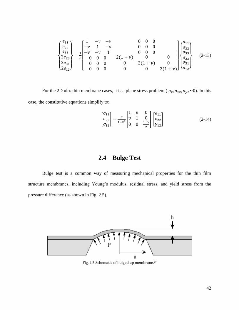
42
(2-13)
For the 2D ultrathin membrane cases, it is a plane stress problem ( ). In this
case, the constitutive equations simplify to:
(2-14)
2.4 Bulge Test
Bulge test is a common way of measuring mechanical properties for the thin film
structure membranes, including Young’s modulus, residual stress, and yield stress from the
pressure difference (as shown in Fig. 2.5).
Fig. 2.5 Schematic of bulged up membrane.77

43
Fig. 2.6 Geometrical reference diagram.77
From the geometry (Fig. 2.6), we can get:
(2-15)
where is the radius of the flat membrane, is the maximum height of the bulged up membrane,
and is the radius of the curvature.
After derivation, the can be represented by and :
(2-16)
From the equilibrium of force for the stress and pressure:
where
, is the thickness of the membrane
Then
(2-17)
From Hooke’s law:
(2-18)
If residual stress, , is not negligible in the membrane:
(2-19)
From the definition, the film strain:

44
(2-20)
where
Then
, into Hooke’s law with residual stress:
(2-21)
When the residual stress dominates, the second term on the right of the equation is
predominant, where the pressure vs. deflection curve is almost linear. As the pressure continues
to increase, the first term on the right of the equation overwhelm the second term. Then the
pressure vs. deflection curve follows cubic trend.77
The previous method is easy and simple. But deviations from this estimation may come
from:
a. Bulge up not truly a spherical section;
b.
;
c.
, when
A more accurate method is to use Hencky’s solution,50
which is the relationship between
the pressure difference and the maximum deflection for a pressurized circular clamped
membrane:
(2-22)

45
where is related to the Poisson’s ratio. From the bulk property, the Poisson’s ratio for
graphene and alumina are 0.16 and 0.24, respectively. For graphene
; For alumina, .78,79
2.5 Harmonic Oscillator
A harmonic oscillator represents many physical devices, including NEMS resonators.
The general equation for a damped harmonic oscillator is:
(2-23)
where is the coefficient related to damping and is the natural frequency.
Depending on the value of and , the equation has three different solutions,
represented in Fig. 2.7.
a) light damping (
), , where
;
b) critical damping (
),
;
c) heavy damping (
),
, where
One key parameter to define damping is the quality factor, which is:80
(2-24)
where is the frequency with max amplitude of the vibration, and are the frequencies at
half-max amplitude, as shown in Fig. 2.8.
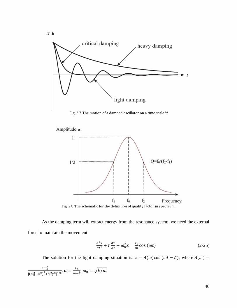
46
Fig. 2.7 The motion of a damped oscillator on a time scale.80
Fig. 2.8 The schematic for the definition of quality factor in spectrum.
As the damping term will extract energy from the resonance system, we need the external
force to maintain the movement:
(2-25)
The solution for the light damping situation is: , where
,
,
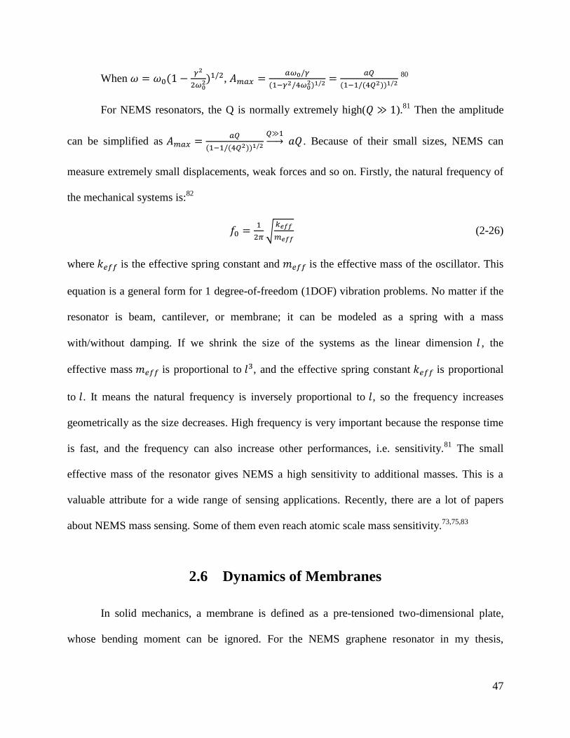
47
When
,
80
For NEMS resonators, the Q is normally extremely high( ).81
Then the amplitude
can be simplified as
. Because of their small sizes, NEMS can
measure extremely small displacements, weak forces and so on. Firstly, the natural frequency of
the mechanical systems is:82
(2-26)
where is the effective spring constant and is the effective mass of the oscillator. This
equation is a general form for 1 degree-of-freedom (1DOF) vibration problems. No matter if the
resonator is beam, cantilever, or membrane; it can be modeled as a spring with a mass
with/without damping. If we shrink the size of the systems as the linear dimension , the
effective mass is proportional to , and the effective spring constant is proportional
to . It means the natural frequency is inversely proportional to , so the frequency increases
geometrically as the size decreases. High frequency is very important because the response time
is fast, and the frequency can also increase other performances, i.e. sensitivity.81
The small
effective mass of the resonator gives NEMS a high sensitivity to additional masses. This is a
valuable attribute for a wide range of sensing applications. Recently, there are a lot of papers
about NEMS mass sensing. Some of them even reach atomic scale mass sensitivity.73,75,83
2.6 Dynamics of Membranes
In solid mechanics, a membrane is defined as a pre-tensioned two-dimensional plate,
whose bending moment can be ignored. For the NEMS graphene resonator in my thesis,

48
membrane dynamics is a better estimation for the movement, compared with plate dynamics. For
the circular membrane with field variable as shown in Fig. 2.9, the motion equation in
polar coordinates is:84
(2-27)
where is the mass per unit area, is the tension per unit length, is the second derivative
to time , is the second derivative to , is the first derivative to , and is the second
derivative to .
With clamped boundary condition (Fig. 2.9):
(2-28)
The vibration modes are shown in Fig. 2.10, with resonant frequency:82
(2-29)
where is the tension across the membrane, is the mass density, is the radius, is the
coefficient depending on the modes: , , ,
, , . For the graphene resonators, the fundamental mode
(m=0, n=1) are the most studied modes.
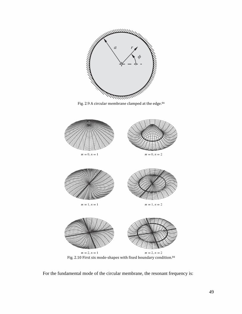
49
Fig. 2.9 A circular membrane clamped at the edge.84
Fig. 2.10 First six mode-shapes with fixed boundary condition.84
For the fundamental mode of the circular membrane, the resonant frequency is:

50
(2-30)
From the Hencky’s solution, we have
with
. If the
contribution of the initial tension can be ignored, combining the Hencky’s solution with the
resonant frequency equation leads to:
(2-31)
where is proportional to the pressure difference cross the circular membrane. This
equation will be used for the ultrathin film mass density calculation in Chapter 5.
2.7 Optical Detection-Interference
Optical interference is a popular technique to detect minor movement of NEMS. For the
detection of NEMS resonators, they use either Michelson interferometer for opaque and
relatively wide resonators,85
or Fabry-Perot interferometer for partially-transparent samples (i.e.
graphene resonators),86-88
as shown in Fig. 2.11. The interference signal comes from the
coherence of two waves. Generally speaking, there are two kinds of coherence: temporal
coherence, and spatial coherence. Temporal coherence measures the average correlation
between itself and after time τ; spatial coherence gives the ability of interference between two
points of the same wave over the time average.
An arbitrary optical wave , where is the complex
wavefunction. The average intensity:
(2-32)
where denotes an ensemble average.
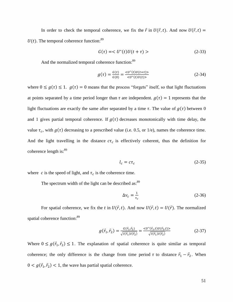
51
In order to check the temporal coherence, we fix the in . And now
. The temporal coherence function:89
(2-33)
And the normalized temporal coherence function:89
(2-34)
where . means that the process “forgets” itself, so that light fluctuations
at points separated by a time period longer than are independent. represents that the
light fluctuations are exactly the same after separated by a time . The value of between 0
and 1 gives partial temporal coherence. If decreases monotonically with time delay, the
value , with decreasing to a prescribed value (i.e. 0.5, or 1/e), names the coherence time.
And the light travelling in the distance is effectively coherent, thus the definition for
coherence length is:89
(2-35)
where is the speed of light, and is the coherence time.
The spectrum width of the light can be described as:89
(2-36)
For spatial coherence, we fix the in . And now . The normalized
spatial coherence function:89
(2-37)
Where . The explanation of spatial coherence is quite similar as temporal
coherence; the only difference is the change from time period to distance . When
, the wave has partial spatial coherence.
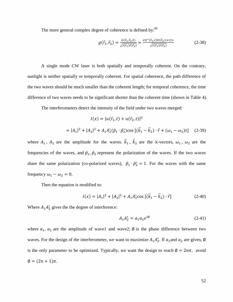
52
The more general complex degree of coherence is defined by:89
(2-38)
A single mode CW laser is both spatially and temporally coherent. On the contrary,
sunlight is neither spatially or temporally coherent. For spatial coherence, the path difference of
the two waves should be much smaller than the coherent length; for temporal coherence, the time
difference of two waves needs to be significant shorter than the coherent time (shown in Table 4).
The interferometers detect the intensity of the field under two waves merged:
(2-39)
where , are the amplitude for the waves. , are the k-vectors, , are the
frequencies of the waves, and , represent the polarization of the waves. If the two waves
share the same polarization (co-polarized waves), . For the waves with the same
frequency .
Then the equation is modified to:
(2-40)
Where gives the the degree of interference:
(2-41)
where , are the amplitude of wave1 and wave2; is the phase difference between two
waves. For the design of the interferometer, we want to maximize . If and are given,
is the only parameter to be optimized. Typically, we want the design to reach , avoid
.
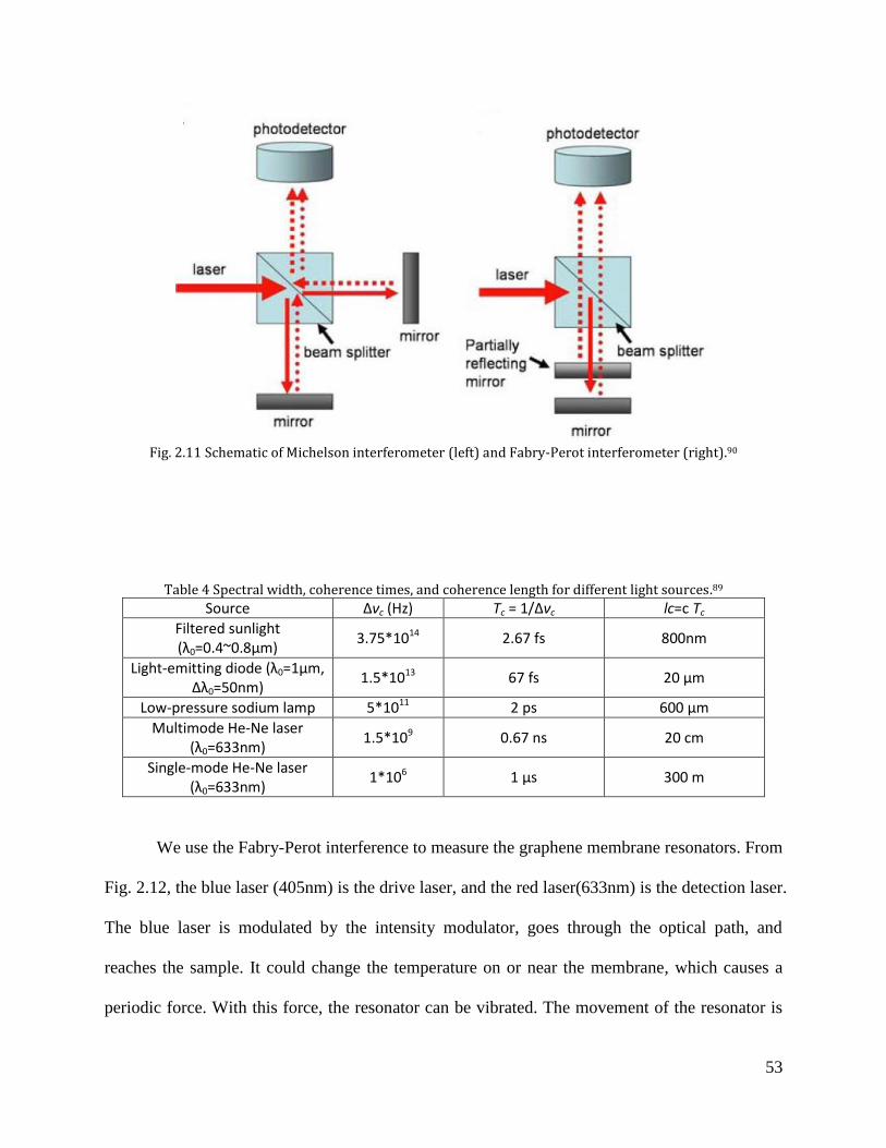
53
Fig. 2.11 Schematic of Michelson interferometer (left) and Fabry-Perot interferometer (right).90
Table 4 Spectral width, coherence times, and coherence length for different light sources.89
Source Δνc (Hz) Τc = 1/Δνc lc=c Τc
Filtered sunlight (λ0=0.4~0.8μm)
3.75*1014 2.67 fs 800nm
Light-emitting diode (λ0=1μm, Δλ0=50nm)
1.5*1013 67 fs 20 μm
Low-pressure sodium lamp 5*1011 2 ps 600 μm
Multimode He-Ne laser (λ0=633nm)
1.5*109 0.67 ns 20 cm
Single-mode He-Ne laser (λ0=633nm)
1*106 1 μs 300 m
We use the Fabry-Perot interference to measure the graphene membrane resonators. From
Fig. 2.12, the blue laser (405nm) is the drive laser, and the red laser(633nm) is the detection laser.
The blue laser is modulated by the intensity modulator, goes through the optical path, and
reaches the sample. It could change the temperature on or near the membrane, which causes a
periodic force. With this force, the resonator can be vibrated. The movement of the resonator is
54
detected by the red laser by Fabry-Perot interference, and then the reflected signal will be
collected by the photo detector. Finally, we can use the network analyzer to analyze the signal.
(a)
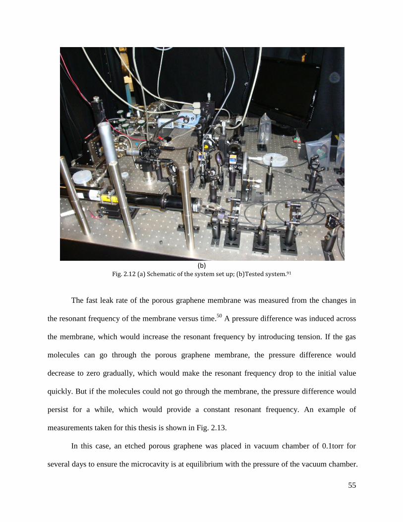
55
(b)
Fig. 2.12 (a) Schematic of the system set up; (b)Tested system.91
The fast leak rate of the porous graphene membrane was measured from the changes in
the resonant frequency of the membrane versus time.50
A pressure difference was induced across
the membrane, which would increase the resonant frequency by introducing tension. If the gas
molecules can go through the porous graphene membrane, the pressure difference would
decrease to zero gradually, which would make the resonant frequency drop to the initial value
quickly. But if the molecules could not go through the membrane, the pressure difference would
persist for a while, which would provide a constant resonant frequency. An example of
measurements taken for this thesis is shown in Fig. 2.13.
In this case, an etched porous graphene was placed in vacuum chamber of 0.1torr for
several days to ensure the microcavity is at equilibrium with the pressure of the vacuum chamber.

56
A pure gas species was then introduced into the same vacuum chamber at a given pressure and
the resonant frequency was measured continuously. The resonant frequency decreases with time
(as the pressure in the microcavity goes from vacuum to the external pressure), and from the rate
of decrease, the leak rate through the membrane can be derived. From Fig. 2.13, the leak rate for
H2, N2, CO2, CH4 were several seconds; but no significant change of the frequency for SF6 for
several minutes. This membrane will be referred to as ‘Bi-4.9Å’, as it is a bilayer membrane with
sieving kinetic diameter of SF6(4.9Å).
Fig. 2.13 Frequency versus time for various gases with a pressure of 100 torr introduced into the vacuum
chamber. Inset: data from the same device with 80torr pressure.50
We can also determine the equation for dn/dt from df/dt:50

57
(2-42)
where is the initial tension of the membrane, is the mass density, is the elastic constant,
is the constant from Hencky’s solution, is the thickness of the membrane, is the radius
of the membrane, is the resonance frequency, is the volume of the microcavity, treated as a
constant in our case, is the gas constant, is the temperature, and
is the change of the
frequency.
From the leak rates of all the membranes, we can get the selectivity for the membranes
(Table 5).
Table 5 Ideal gas separation factors for membrane ‘Bi-4.9Å ’.50

58
2.8 Conclusions
This chapter introduced the basis of solid state mechanics and dynamics for NEMS,
especially for graphene NEMS resonators. Optical detection for graphene resonators was
introduced. In next chapter, we will review ALD, the material involved in one of the projects.

59
Chapter 3 Atomic Layer Deposition (ALD)
3.1 Introduction
ALD becomes a key technique for science and technology progress, which can be used to
achieve ultrathin films in our lab. ALD reaction is continuous and almost pin hole free, even for
the high aspect ratio.92
Many of the ALD materials are stable, which can be used in hash
environments. What’s more, there are numerous applications for flexible ultrathin insulating or
oxide films, which may come from ALD.
3.2 Atomic Layer Deposition
Atomic layer deposition (ALD) becomes an important surface technology with
motivation towards scaling down microelectronic devices. Semiconductor processing is the main
driver for ALD, since ALD meets the needs of continuous and pinhole-free films of
semiconductor devices. Other applications come from magnetic read/write heads93
and diffusion
barrier coating.94
Most ALD processes are based on binary reaction sequences, as shown in Fig.
3.1. Some materials have been grown by ALD, shown in Fig. 3.2.
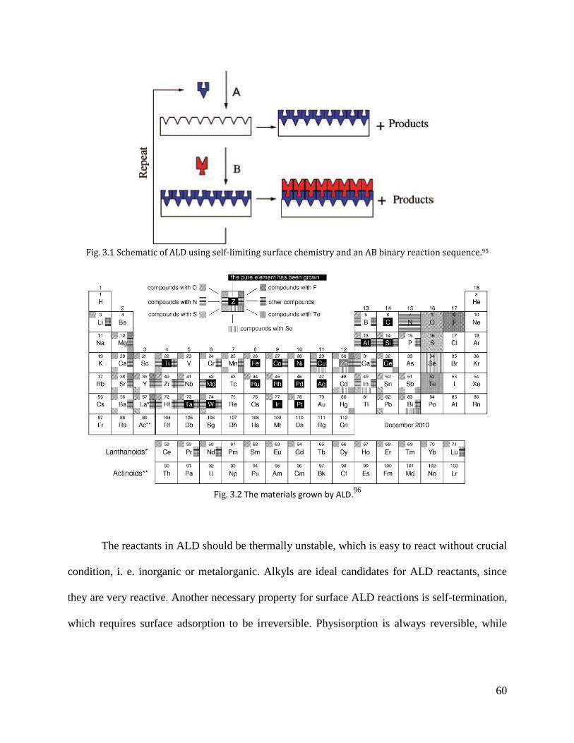
60
Fig. 3.1 Schematic of ALD using self-limiting surface chemistry and an AB binary reaction sequence.95
Fig. 3.2 The materials grown by ALD.
96
The reactants in ALD should be thermally unstable, which is easy to react without crucial
condition, i. e. inorganic or metalorganic. Alkyls are ideal candidates for ALD reactants, since
they are very reactive. Another necessary property for surface ALD reactions is self-termination,
which requires surface adsorption to be irreversible. Physisorption is always reversible, while

61
chemisorptions can be reversible or irreversible. So the adsorption in ALD is limited to
irreversible chemisorptions. The adsorption rate is defined by:
(3-1)
where is the adsorption rate, is desorption rate, is the adsorption rate constant, is the
desorption rate constant, is partial pressure, and is the chemisorption coverage. After
saturation the adsorption rate is zero, Langmuir isotherm gives the chemisorption coverage in
equilibrium:
(3-2)
For irreversible adsorption, the equilibrium constant , then . So the
chemisorption coverage becomes:
(3-3)
The chemisorption mechanisms in ALD have three different kinds: a. ligand exchange, b.
dissociation, c. association, which is shown in Fig. 3.3. In ligand exchange, the ligand is
combined with a surface group and released as a gaseous reaction. For dissociation, the reactant
molecule is separated onto reactive sites on the surface. According to association, the reactant
forms a coordinative bond with a reactive site, and no ligand is released.97
The reason for the self-limiting (self-termination) is a finite number of surface sites can
only deposit a certain number of surface species. The factors causing saturation are steric
hindrance, and the number of reactive surface sites. In some situations, even though space
remains available on the surface, no bonding sites are accessible. The reaction continues until
steric hindrance stops it, which causes growth of less than a monolayer per cycle.98
Temperature

62
can also affect the growth per cycle (GPC) by affecting the number and type of reactive sites on
the surface, and through changing the preferred reaction mechanisms. What’s more, another
issue to impact GPC is the number of cycles. From the very beginning, ALD reaction cycle
happens on the surface of the original substrate material. Then, it occurs on a surface with both
the original substrate and the ALD-grown material. Finally, it reacts on a surface with only the
ALD grown material exposed. Different steps will give you different GPC. Generally speaking,
the growth mode has three types (as shown in Fig. 3.4): a. two dimensional growth, b. island
growth, and c. random deposition.
Fig. 3.3 Chemisorption mechanisms for ALD.97
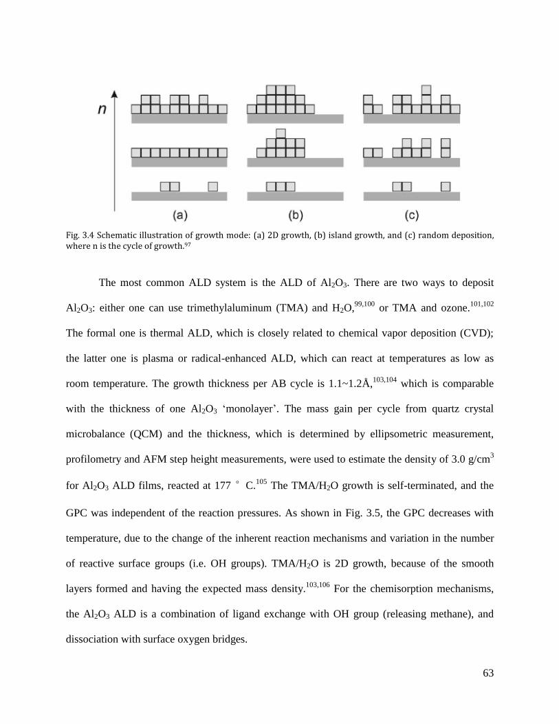
63
Fig. 3.4 Schematic illustration of growth mode: (a) 2D growth, (b) island growth, and (c) random deposition, where n is the cycle of growth.97
The most common ALD system is the ALD of Al2O3. There are two ways to deposit
Al2O3: either one can use trimethylaluminum (TMA) and H2O,99,100
or TMA and ozone.101,102
The formal one is thermal ALD, which is closely related to chemical vapor deposition (CVD);
the latter one is plasma or radical-enhanced ALD, which can react at temperatures as low as
room temperature. The growth thickness per AB cycle is 1.1~1.2Å,103,104
which is comparable
with the thickness of one Al2O3 ‘monolayer’. The mass gain per cycle from quartz crystal
microbalance (QCM) and the thickness, which is determined by ellipsometric measurement,
profilometry and AFM step height measurements, were used to estimate the density of 3.0 g/cm3
for Al2O3 ALD films, reacted at 177 °C.105
The TMA/H2O growth is self-terminated, and the
GPC was independent of the reaction pressures. As shown in Fig. 3.5, the GPC decreases with
temperature, due to the change of the inherent reaction mechanisms and variation in the number
of reactive surface groups (i.e. OH groups). TMA/H2O is 2D growth, because of the smooth
layers formed and having the expected mass density.103,106
For the chemisorption mechanisms,
the Al2O3 ALD is a combination of ligand exchange with OH group (releasing methane), and
dissociation with surface oxygen bridges.

64
Fig. 3.5 GPC of TMA/H2O vs temperature.103,107-113
There are different types of ALD reactors. One kind of reactors’ reactants is exposed
without using a carrier gas and sometimes with throttled pumping.103,114,115
On the other hand,
some ALD reactors’ reactants are exposed with a carrier gas (most of the flow is inert gases)
flowing through the reactor.104,116
Some ‘batch’ reactors can deposit on many samples
simultaneously.
High- K dielectric ALD Al2O3 has been studied as a candidate to replace SiO2 as gate
electrics. Complementary metal oxide semiconductor (CMOS) field effect transistors (FET) have
continued to be improved, following Moore’s law for decades.117
More and more devices in the
same chip require smaller and smaller sizes of devices. But once the thickness of SiO2 is smaller
than 2nm, the strong gate leakage current exists from tunneling electrons through SiO2.117
Thus
new material is desired to replace SiO2 as a gate oxide.
The source-drain current of the FET controls by the gate capacitance:117
(3-4)
65
where is the vacuum permittivity, is the area of the capacitance, is the relative
permittivity, and is the thickness of the oxide. Tunneling current is extremely sensitive to the
distance, which means increasing the thickness will dramatically reduce the leakage current. But
adding the thickness of the oxide will also decrease the gate capacitance. The solution is to seek
a high-K dielectric with thick oxide, which will limit the leakage current with relatively high gate
capacitance.
Six conditions need to be satisfied to choose high-K dielectric as gate electrics.117
(a) It
needs high enough K value; (b) It needs to be thermodynamically stable, due to direct contact
with Si; (c) It must be kinetically stable, since the high temperature annealing for the device is
needed to release the impurities; (d) It should act as an insulator, which means the band offset of
Si should be over 1 eV; (e) It needs to have good electrical inter face with Si; (f) It must have
few bulk electrically active defects.117
Al2O3 satisfies all the requirements for the high-K
dielectric as gate electrics. Compared with other deposition methods, ALD Al2O3 has excellent
coverage, good purity, pin-hole free, atomic thickness, and large area.117
Combination of ALD Al2O3 and carbon nanotube (CNT) or graphene leads to new
applications. Graphene or CNT insulated and protected by passivation layer is necessary for its
applications, such as, building blocks for the fabrication of nanodevices,118
field effect
transistors,119,120
surrounded gate transistor,121,122
field-emission electron sources,123
and
nanoprobes for microscopy.124
ALD Al2O3 gives perfect protection as passivation layer for CNT
or graphene. But direct deposition is difficult, since the surface of graphene or CNT is inert and
does not contain chemical species that allow for the reaction. Consequently, isolated Al2O3
nanospheres are grown on defects of CNT and graphene, and nanoribbons are formulated along
the step edges of the graphene surface.125-127
Pretreatments are needed for the Al2O3 ALD

66
coating. Wet chemistry treatments, including inorganic or organic approaches,128-135
are effective
as pretreatments. But the liquid-based techniques are experimentally tedious and may not be
scaled-up, and its functionalization changes the hybridization of CNT or graphene. Another
method is using ozone or O2 plasma to increase the surface energy of graphene before the
coating, which introduced defects in the graphene lattice.136,137
Certain substrate such as Cu may
enhance the coating, but it is not a universal method for an arbitrary substrate or suspended
graphene/CNT.138
Compared with previous pretreatments method, we prefer NO2/TMA
pretreatment. It is simple, which can be finished in the same instrument as the coating. It is easy
to scale up, and the only limit is the volume of the ALD coating chamber. This method does not
change the property of CNT or graphene, and do not introduce any extra defects. The classical
recipe is 50 cycles of NO2/TMA at room temperature. NO2 monolayer is physisorbed to
CNT/graphene, and TMA is adsorbed onto the NO2. This forms a self-terminationg monolayer
around CNT or on graphene, providing an adhesion layer for the nucleation and growth of Al2O3
ALD films, as shown in Fig. 3.6.125,139,140
(a) (b)
Fig. 3.6 (a) Schematic of NO2/TMA functionalization mechanism. NO2 is adsorbed on the CNT surface, followed by TMA.139 (b) Illumination of oxide deposition process on graphene. NO2/TMA pretreatment is followed by H2O/TMA growth.140
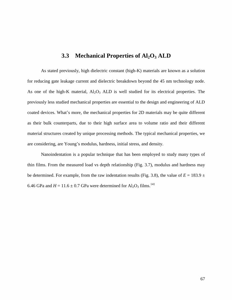
67
3.3 Mechanical Properties of Al2O3 ALD
As stated previously, high dielectric constant (high-K) materials are known as a solution
for reducing gate leakage current and dielectric breakdown beyond the 45 nm technology node.
As one of the high-K material, Al2O3 ALD is well studied for its electrical properties. The
previously less studied mechanical properties are essential to the design and engineering of ALD
coated devices. What’s more, the mechanical properties for 2D materials may be quite different
as their bulk counterparts, due to their high surface area to volume ratio and their different
material structures created by unique processing methods. The typical mechanical properties, we
are considering, are Young’s modulus, hardness, initial stress, and density.
Nanoindentation is a popular technique that has been employed to study many types of
thin films. From the measured load vs depth relationship (Fig. 3.7), modulus and hardness may
be determined. For example, from the raw indentation results (Fig. 3.8), the value of E = 183.9 ±
6.46 GPa and H = 11.6 ± 0.7 GPa were determined for Al2O3 films.141

68
Fig. 3.7 FESEM images of the residual impression remaining after indentation to (a) Al2O3, and (b) SiO2
coatings on Si.141
Fig. 3.8 load vs. depth for 500nm thick Al2O3 film on Si.
141
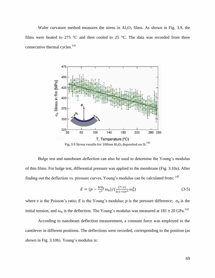
69
Wafer curvature method measures the stress in Al2O3 films. As shown in Fig. 3.9, the
films were heated to 275 °C and then cooled to 25 °C. The data was recorded from three
consecutive thermal cycles.141
Fig. 3.9 Stress results for 100nm Al2O3 deposited on Si.
141
Bulge test and nanobeam deflection can also be used to determine the Young’s modulus
of thin films. For bulge test, differential pressure was applied to the membrane (Fig. 3.10a). After
finding out the deflection vs. pressure curves, Young’s modulus can be calculated from: 142
(3-5)
where is the Poisson’s ratio; is the Young’s modulus; is the pressure difference; is the
initial tension, and is the deflection. The Young’s modulus was measured at 181 ± 20 GPa.143
According to nanobeam deflection measurement, a constant force was employed to the
cantilever in different positions. The deflections were recorded, corresponding to the position (as
shown in Fig. 3.10b). Young’s modulus is:
70
(3-6)
where is the Young’s modulus, is the deflection, the width, the contact point, the
force, and the thickness of the cantilever.144
From the fit of the measured data, they got the
Young’s modulus is 168 ± 8 GPa for the 100nm-thick cantilever, and it is 182 ± 32 GPa for the
50nm-thick cantilever.143
(a) (b)
Fig. 3.10 (a) Bulge test results; (b) AFM-based nanobeam deflection measurements.143
Craighead’s group demonstrated the ability to simultaneously measure Young’s modulus
and density of ~21nm ALD alumina by a resonance method using an interferometer. They have
coated ALD films on both sides of the Si cantilever resonators (Fig. 3.11 a-h). The resonant
frequencies are very sensitive to the mass change of the NEMS resonators, and the coating of the
ALD will shift down the frequencies. They compared the resonant frequencies of both in-plane
and out-of-plane modes for the resonators before and after coating (Fig. 3.11 i-j). From the
comparison, the Young’s modulus and density of coated films were deduced to be ~170 GPa and
3g/cm3, respectively.
145

71
Fig. 3.11 Fabrication sequence of nanomechanical cantilevers devices and experimental schematic for
measuring the NEMS resonators.145
3.4 Conclusions
ALD is an important technique mostly used in coating, but also can be used to create a
structured membrane. The state of the art for the mechanical properties of Al2O3 ALD was
reviewed. In chapter 5, we will present newly-determined mechanical properties of ultrathin
ALD films.
72
Chapter 4 Single Nanopore Molecular Valves in
Graphene for Controlling Gas Phase Transport
4.1 Introduction
The ability to control the quantity and location of a single file molecular flux to a precise
location in space has important applications for nanoscale 3D printing, catalysis, and sensor
design. Barrier materials containing pores with molecular dimensions have been used to control
molecular compositions in the gas phase, but unlike their aqueous counterparts, none has enabled
an ability to observe or control single pore transport.146-156
Herein, we demonstrate gas transport
through atomically thin, monolayer graphene opened with a single (nominally) molecular-sized,
sub-nm pore demonstrating the ability to detect and control the gas flux. This is accomplished
using ~nm sized gold clusters formed on the surface of the graphene. Such clusters migrate and
partially block the pore. We also observe stochastic switching of small magnitude in the gas flux
indicative of modulation by a single pore even without gold clusters. The stochastic switching is
analyzed using a Hidden Markov Model to fit to discrete and repeatable states, and the switching
frequency is used to estimate the energy of the transition that occurs. This work presents an
example of creating single nanopore molecular valves to control gas phase transport through a
comparably-sized pore.9,61-63,90,157-164
These nanopore molecular valves open possibilities for
unique sensors, catalytic processes, and approaches to molecular synthesis based on the
controllable switching of a molecular gas flux reminiscent of ion channels in biological cell
membranes and solid state nanopores.38
73
4.2 Material and Method
The methods for device fabrication and pressurization follow closely references. 8,50,79,165
Suspended graphene membranes were fabricated using mechanical exfoliation on silicon oxide
substrates with predefined etched wells. The wells were defined by photolithography on an
oxidized silicon wafer with 90nm silicon oxide on top and have a diameter of 4~5 μm. Reactive
Ion Etching was used to etch the wells to a depth of 400~1000 nm, and the ‘scotch tape’ method
was used to deposit graphene over the wells. The gold atoms were evaporated onto the graphene
in vacuum (CVC 3-boat thermal evaporator, at 0.1 Å/s for less than 0.5 s).
To pressurize the inside of the microcavity, we put the sample into a high pressure
chamber with a certain gas species at a prescribed pressure, which we call the charging pressure.
After several hours or days, depending on the gas species used, the pressure in the microcavity
comes to equilibrium with the charging pressure. The pristine graphene sheet is impermeable to
any gases, but the gas can diffuse through the silicon oxide substrate. To reach pressure
equilibrium, we wait 4~30 days, which is longer than the time for equilibrium to make sure the
accuracy of the measurements.
After measuring the leaking rate for the pristine graphene, we etched pores by exposing
the graphene membranes to a UV lamp (λ1=185nm, λ2=254nm) under ambient conditions. We
first pressurized them with pure H2 up to 200 kPa above ambient pressure. After the microcavity
reached equilibrium we removed it from the pressure chamber and measured the deflection using
AFM. We continue with a series of short UV exposures (less than one minute) followed by quick
AFM scans (few minutes). Once a pore is created whose size is between H2 and N2, then the
deflection abruptly changes from positive to negative. Once a pore is created, the leak rate is

74
dominated by transport through the pores and 1~12 hours of pressurization, depending on the gas
species, is sufficient for equilibrium.
4.3 Leak Rate for Pristine Graphene
The leak rate can be derived from a mass balance on the microcavity using the ideal gas
law and Hencky’s solution for a clamped circular membrane and follows closely reference:50
2 3 2
04 4
1[3 ]b atm
dn Et Et dK V V P K C a
dt RT a a dt
(4-1)
where R is the gas constant, T is the temperature, E = 1 TPa is the Young’s modulus, t = 0.335
nm is the thickness of the membrane, a is the radius of the membrane (microwell), V0 is the
microcavity volume at zero deflection, Vb is the bulged up volume calculation from deflection,
Patm is the ambient pressure, δ is the maximum deflection of the membrane, K(ν = 0.16) = 3.09,
and C(ν = 0.16) = 0.52 are constants determined by the Hencky’s solution.
The maximum deflection versus time was measured for pristine unetched graphene
membranes (Fig. 4.1). The samples were inserted into the high pressure chamber with ~200 kPa
charging H2. After few weeks, the internal pressure of the microcavity reached equilibrium with
the charging pressure. Continuous AFM scanning was taken during the first 100 min of removal
from the pressure chamber, and the deflection decreased by a few nanometers. From the slope of
the deflection vs. time and equation 4-1, we determine that the permeance is ~6 x 10-25
mol s-1
Pa-1
,
which is one order of magnitude slower than the H2 permeance of the porous graphene
membranes.
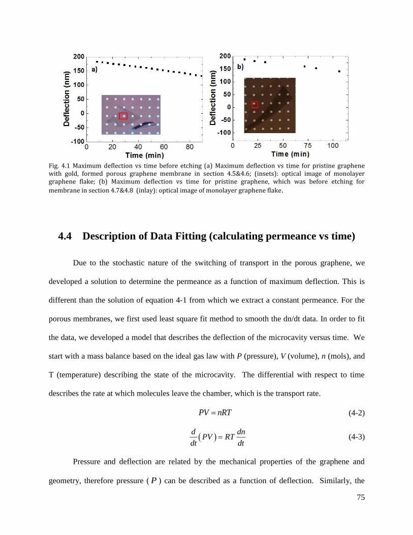
75
Fig. 4.1 Maximum deflection vs time before etching (a) Maximum deflection vs time for pristine graphene with gold, formed porous graphene membrane in section 4.5&4.6; (insets): optical image of monolayer graphene flake; (b) Maximum deflection vs time for pristine graphene, which was before etching for
membrane in section 4.7&4.8 (inlay): optical image of monolayer graphene flake.
4.4 Description of Data Fitting (calculating permeance vs time)
Due to the stochastic nature of the switching of transport in the porous graphene, we
developed a solution to determine the permeance as a function of maximum deflection. This is
different than the solution of equation 4-1 from which we extract a constant permeance. For the
porous membranes, we first used least square fit method to smooth the dn/dt data. In order to fit
the data, we developed a model that describes the deflection of the microcavity versus time. We
start with a mass balance based on the ideal gas law with P (pressure), V (volume), n (mols), and
T (temperature) describing the state of the microcavity. The differential with respect to time
describes the rate at which molecules leave the chamber, which is the transport rate.
PV nRT (4-2)
d dn
PV RTdt dt
(4-3)
Pressure and deflection are related by the mechanical properties of the graphene and
geometry, therefore pressure ( P ) can be described as a function of deflection. Similarly, the
76
volume of the well is directly related to the deflection. Therefore the ideal gas law can be
written with those two terms as function of the deflection.
( ( ) ( ))d d P V dnRT
dt d dt
(4-4)
The relation between pressure and deflection is described by the following equation.
3 303 14 2
4( )atm atm
SEtKP P p p P
a a
(4-5)
where 0S is the initial surface tension of the graphene which has a well known value of
0.1N/m.8,165
The mechanical constants used are well established from numerous experiments of
graphene membranes in a similar geometry.7,50,79,165
For convenience, the parameters have been
lumped into the constants 1p and 3p . The relation between volume and deflection is described
by the following equation.
2
0 1 0V C a V V (4-6)
The constants for linear deflection term have been lumped together into 1 for
convenience.
The normalized dn/dt, which is proportional to permeance, is calculated by dividing dn/dt
by the pressure difference of the effusing gas species. Classical effusion results in a linear
relation between the rate of transport and the pressure difference, and therefore we define a
constant value for normalized dn/dt, represented by k . The gas within the microcavity is
assumed to be pure, and therefore total pressure ( )P is equal to the partial pressure of the gas.
extP is the partial pressure of the gas species in atmosphere and is approximately zero for all of
the gases tested (except O2 and N2).

77
( )ext
dnk P P
dt (4-7)
By assuming this form for dn/dt, the differential equation can be written in terms of the
deflection as follows.
( ( ) ( ))
( )ext
d d P VRTk P P
dt d
(4-8)
2 3 3
1 1 0 1 1 3 0 3 1 1 32 3 4 ( )atm atm ext
dP pV p p V p RTk P P p p
dt
(4-9)
The dependence on the deflection is represented as a single arbitrary function, y.
2 3
1 1 0 1 1 3 0 3 1
3
1 3
2 3 (4 )atm
atm ext
P pV p p V py
P P p p
(4-10)
d
y RTkdt
(4-11)
The differential equation is separable and can be solved.
0 0
t
y d RTk dt
(4-12)
0 Y Y RTkt (4-13)
The resulting form is a line. The values of the integral, ( )Y , can be calculated
numerically for each experimental deflection point. A segment of these values is fit using the
analytical least squares line fit, and gives results for 0( )Y and k when temperature is known.
For the results of permeance or flux, the fitting method is applied to a segment of 5 data
points, and the resulting values are assigned to the center data point. A value of k, the permeance,
is calculated at each point by proceeding through the data set in this manner. Permeance values
following only include points with deflection above 50 nm. Points below 50 nm were excluded
because small errors in the pressure correlation, and small amounts of air in the microcavity in
78
some runs results in large errors in the permeance calculation at points lower than 50 nm
deflection. When a full five points aren’t available for the points at the beginning and end of the
deflection data set, only the three or four nearest points are used to fit a value of permeation.
4.5 Stochastic Switching of Gas Transport by AuNC
We studied 2 types of nanopore molecular valves: a porous single layer of suspended
graphene with no gold nanoclusters on its surface (PSLG) and a porous single layer of suspended
graphene on top of which we evaporated gold nanoclusters (PSLG-AuNCs). To fabricate both
types of devices, we start with suspended pristine monolayer graphene. The graphene is
mechanically exfoliated over predefined etched wells on a silicon substrate with 90 nm of
thermal silicon oxide on top. This forms a graphene-sealed microcavity which confines a ~µm3
volume of gas underneath the suspended graphene. For the PSLG-AuNCs samples, gold atoms
are evaporated onto the graphene after exfoliation and prior to poration. Molecular sized pores in
the graphene are introduced using UV-induced oxidation.50
In the first few hours after UV-
induced oxidation, the gold clusters are observed to migrate and congregate on the surface of the
graphene (Fig. 4.2a-b).
A pressurized blister test is used to determine the leak rate out of the graphene sealed
microcavity.50
The microcavity is filled with 300 kPa of pure H2, and the membrane is bulged up
due to the pressure difference across the membrane (Fig. 4.3a and d). We then monitor the
deflection of the membrane using an AFM (Fig. 4.3d-f). For the PSLG-AuNC device, the leak
rate of gas out of the microcavity is slow initially, and the membrane deflection changes slowly

79
with time (Fig. 4.3d). A fit to a membrane mechanics model is shown as a red line. During
scanning there is a sudden jump in the deflection and a much faster leak rate is observed (Fig.
4.3e). This change from bulged up to bulged down occurs in ~30 s and is indicative of a rapid
leaking of all of the H2 gas inside the microcavity, while any leak of air back into the cavity is
much slower. A line cut through the center of the membrane during this process is shown in Fig.
4.4. From the line cut (blue lines in Fig. 4.3 d-f), we can see the maximum deflection drops from
147nm to -115nm in ~1 minute (Fig. 4.5). We attribute this sudden change in the deflection to
migration of the gold nanoclusters on the surface of the membrane that “opened” a single pore in
the graphene membrane allowing a fast leak rate (Fig. 4.3a-c). A single pore in the graphene
membrane is likely responsible for the sudden change in permeance since it is unlikely that
multiple identical pores opened simultaneously.
Fig. 4.2 AFM amplitude images showing the movement of gold nanoparticles on a suspended graphene membrane.

80
Fig. 4.3 (a-c) Schematic of the gold nanoparticles (yellow solid circles) blocking and unblocking the pore on the monolayer graphene membrane; (d-f) AFM height images capturing the deflection change in (a-c).
Fig. 4.4 Deflection vs. position through the center of the membrane in Fig. 4.3 (d-f).

81
Fig. 4.5 Maximum deflection vs. time for the dramatic leak rate change. The solid red line is a fit to the data before switching using the membrane mechanics model.
Fig. 4.5 plots an extrapolated fit of the deflection data before the sudden drop in
deflection. This extrapolation represents the expected trajectory if the pore had continued in the
blocked state at the start of the run. It was calculated by numerically linearizing the deflection
data prior to the sudden drop (0 to 12 minutes) via equation 4-12 to the form of equation 4-13.
From the analytical least squares fit, values for the two parameters, 0( )Y and k , can be
determined based on all the points in the range of 0 to 12 minutes.
To create a fit and extrapolation for the deflection, a set of artificial evenly spaced
deflection values between the maximum and minimum deflections are put in the form of
equation 4-13. The fitted values of the two parameters, Y(δ0) and k, are used to solve for time at
each of the artificial deflection points. Then the artificial deflection points are plotted against the
calculated times as the fit and extrapolation.
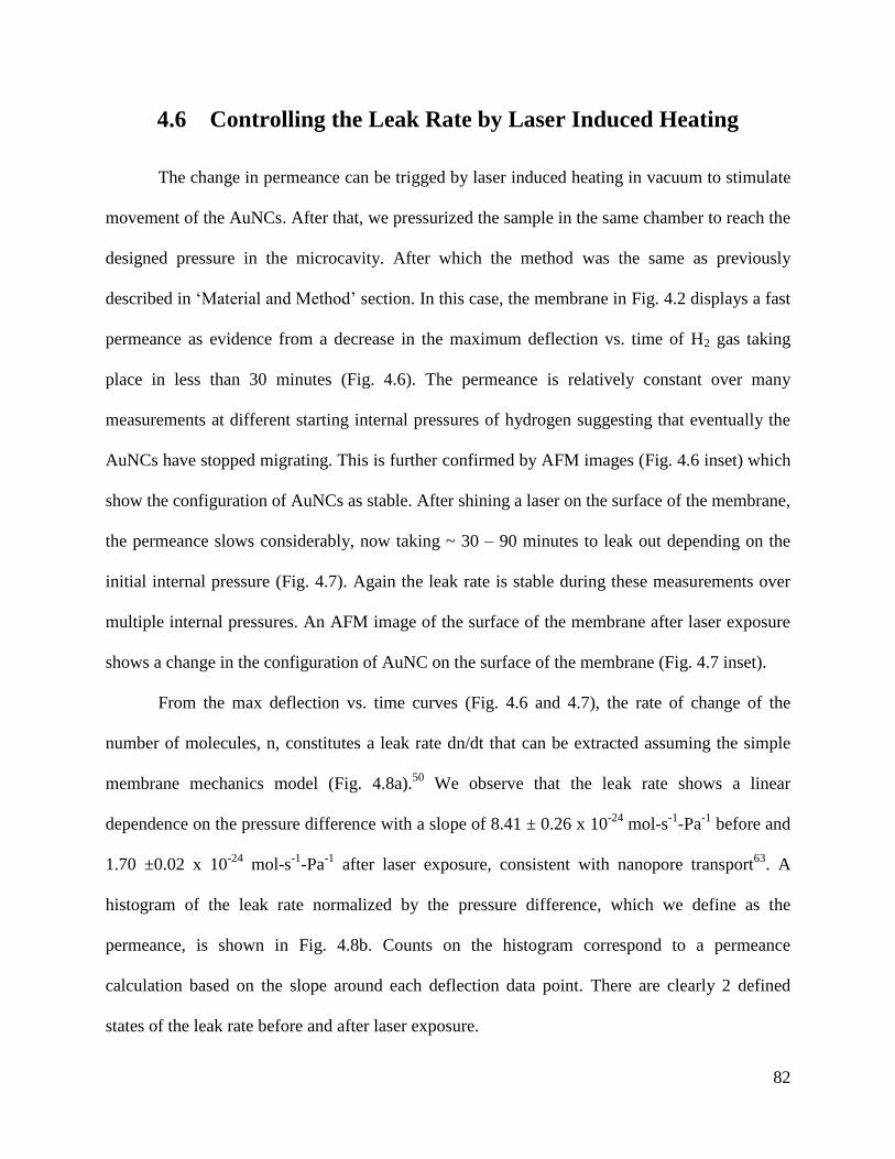
82
4.6 Controlling the Leak Rate by Laser Induced Heating
The change in permeance can be trigged by laser induced heating in vacuum to stimulate
movement of the AuNCs. After that, we pressurized the sample in the same chamber to reach the
designed pressure in the microcavity. After which the method was the same as previously
described in ‘Material and Method’ section. In this case, the membrane in Fig. 4.2 displays a fast
permeance as evidence from a decrease in the maximum deflection vs. time of H2 gas taking
place in less than 30 minutes (Fig. 4.6). The permeance is relatively constant over many
measurements at different starting internal pressures of hydrogen suggesting that eventually the
AuNCs have stopped migrating. This is further confirmed by AFM images (Fig. 4.6 inset) which
show the configuration of AuNCs as stable. After shining a laser on the surface of the membrane,
the permeance slows considerably, now taking ~ 30 – 90 minutes to leak out depending on the
initial internal pressure (Fig. 4.7). Again the leak rate is stable during these measurements over
multiple internal pressures. An AFM image of the surface of the membrane after laser exposure
shows a change in the configuration of AuNC on the surface of the membrane (Fig. 4.7 inset).
From the max deflection vs. time curves (Fig. 4.6 and 4.7), the rate of change of the
number of molecules, n, constitutes a leak rate dn/dt that can be extracted assuming the simple
membrane mechanics model (Fig. 4.8a).50
We observe that the leak rate shows a linear
dependence on the pressure difference with a slope of 8.41 ± 0.26 x 10⁻²⁴
mol-s-1
-Pa-1
before and
1.70 ±0.02 x 10⁻²⁴
mol-s-1
-Pa-1
after laser exposure, consistent with nanopore transport63
. A
histogram of the leak rate normalized by the pressure difference, which we define as the
permeance, is shown in Fig. 4.8b. Counts on the histogram correspond to a permeance
calculation based on the slope around each deflection data point. There are clearly 2 defined
states of the leak rate before and after laser exposure.

83
Fig. 4.6 Maximum deflection of the graphene membrane before focusing a laser beam at the center of the membrane. Different colors represent different charging pressures. The charging pressure is from 200 kPa to 700 kPa to 200 kPa, in 100 kPa increments; (inset) AFM amplitude images of the graphene membrane corresponding to the state of the graphene membrane for the measurements.
Fig. 4.7 Maximum deflection of the graphene membrane after focusing a laser beam at the center of the membrane. Different colors represent different charging pressures. The charging pressure is from 200 kPa to 850 kPa, in 50 kPa, 100 kPa, or 150 kPa increments. (inset) AFM amplitude images of the graphene membrane corresponding to the state of the graphene membrane for the measurements.
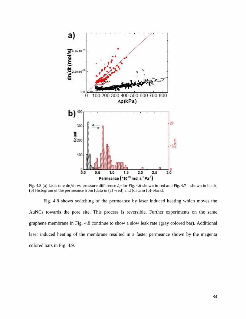
84
Fig. 4.8 (a) Leak rate dn/dt vs. pressure difference Δp for Fig. 4.6-shown in red and Fig. 4.7 – shown in black; (b) Histogram of the permeance from (data in (a) –red) and (data in (b)-black).
Fig. 4.8 shows switching of the permeance by laser induced heating which moves the
AuNCs towards the pore site. This process is reversible. Further experiments on the same
graphene membrane in Fig. 4.8 continue to show a slow leak rate (gray colored bar). Additional
laser induced heating of the membrane resulted in a faster permeance shown by the magenta
colored bars in Fig. 4.9.
85
Fig. 4.9 Histogram of the permeance from (data in gray) to (data in magenta) by laser induced heating again.
Gas transport through the porous graphene membranes can be modeled using classical
effusion. When the pore size is smaller than the mean free path of the molecule, classical
effusion dictates that the time constant for the decay of the number of molecules in the graphene
sealed microcavity is given by:
2
R
wMV
T
(4-14)
where V is the volume of the container, γ is the transmission coefficient, Mw is the molecular
mass, R is the ideal gas constant, and T is the temperature.52
The transmission coefficient, γ,
incorporates both the physical geometry of the pore, and any energy barrier from molecular
interactions between the molecule and the pore. Due to the small volume of gas in the graphene
sealed microchamber (~1 µm3), the time constant for the effusion due to a single defect can be
considerably long (tens of minutes) making our geometry ideally suited for measuring the leak
rate through a single sub-nm pore and for observing sub-Å2 changes in the transmission
coefficient. Correspondingly, the leak rate dn/dt assuming classical effusion is given by:
dn
dt 2π Rw
pM T
(4-15)
where Δp is the pressure difference across the membrane 63
. A plot of dn/dt vs. Δp shows a linear
dependence further supporting classical effusion (Fig. 4.8a). The transmission coefficient can be

86
deduced from the slope and changes from 0.15 Å2 (before) to 0.03 Å2
(after) laser heating. The
transmission coefficient is the geometric area of the pore (a few Å2) multiplied by a transmission
probability that an impinging gas atom or molecule has sufficient energy to pass through the
potential barrier of the pore. Hence, γ is considerably smaller than the cross sectional area of the
test gas H2 (2.89 Å) providing further evidence that the pore is on the order of the kinetic
diameter of H2 and we are measuring small changes in the energy barrier from molecular
interactions between the gas and pore mouth.
4.7 Influence of Gas Species on Leak Rate
The ability to observe small changes in γ allows us to vary the molecular size and study
how that influences gas transport in the same SLGM. For this study, we used a single SLGM that
contained no AuNCs. The leak rate, dn/dt, of helium gas through SLGM shows a linear
dependence on Δp and is relatively constant over a range of Δp from 200 kPa to 700 kPa (Fig.
4.10 inset). This agrees with classical effusion with a slope equal to 1.5 ± 0.01 x 10⁻²³
mol-s-1
-Pa-
1 corresponding to γ = 0.36 Å2
(Fig. 4.10). The permeance for other noble gases, Ar, Ne, as well
as He, are shown as a histogram with average values and standard deviations of 4.1 ±2.1 x 10⁻²⁵
,
2.5 ±1.6 x 10⁻²⁴
, and 1.5 ±0.2 x 10⁻²³
mol-s-1
-Pa-1
, respectively (Fig. 4.11). This follows a trend of
a slower leak rates for larger gas atoms. In addition to the noble gases, we measured the leak rate
of the non-noble gas molecules, H2, CO2, and N2O both before and after introducing the
molecular-sized pores (Fig. 4.12). Data for the non-porated graphene was taken on a separate but
similar monolayer graphene membrane and the measured leak rates agree well with a leak
87
primarily through the underlying silicon oxide substrate.8,50,79
In all cases, there was a
considerable increase in the leak rate after poration supporting that the leak rate is primarily
through the molecular-sized pore.
We can deduce the transmission coefficient as a function of the kinetic diameter for all
the gases measured. As expected for the noble gases, the transmission coefficient increases as the
kinetic diameter decreases: (Ar) 0.027 ±0.017 Å2, (Ne) 0.14 ±0.09 Å2
, and (He) 0.36 ±0.05 Å2
(Fig. 4.13), further confirming that the pore size is on the order of the kinetic diameter and
showing the influence of the molecular size on γ. In addition, the leak rate of H2, roughly follows
the trend observed with the noble gas atoms. However, CO2 and N2O follow a very different
trend (inset Fig. 4.13). Their leak rates and transmission coefficients are considerably larger than
one would expect from their kinetic diameter (CO2) 0.65 ±0.52 Å2, and (N2O) 1.52 ±1.21 Å2
. We
attribute this to chemical interactions that N2O and CO2 have with the pore which lowers the
energy barrier to transport. These experiments demonstrate that gas transport of polar gas
molecules clearly shows a strong influence on chemical interactions between the molecule and
the pore consistent with recent theoretical calculations.161,163
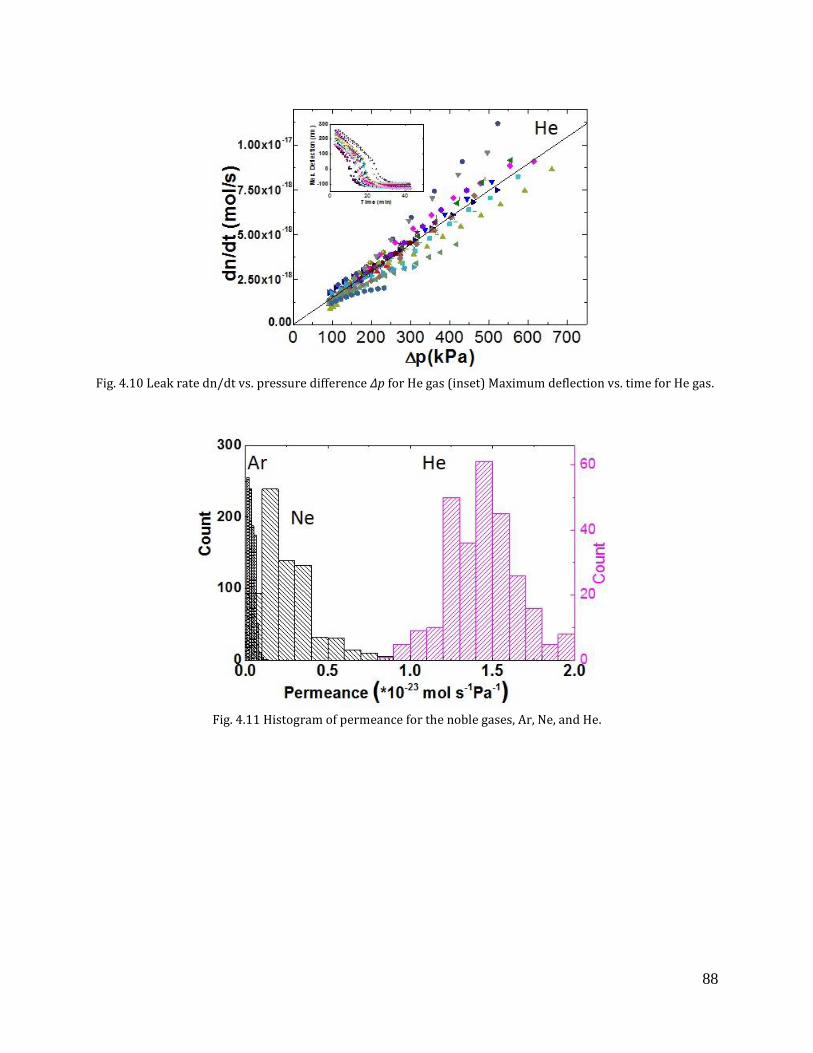
88
Fig. 4.10 Leak rate dn/dt vs. pressure difference Δp for He gas (inset) Maximum deflection vs. time for He gas.
Fig. 4.11 Histogram of permeance for the noble gases, Ar, Ne, and He.
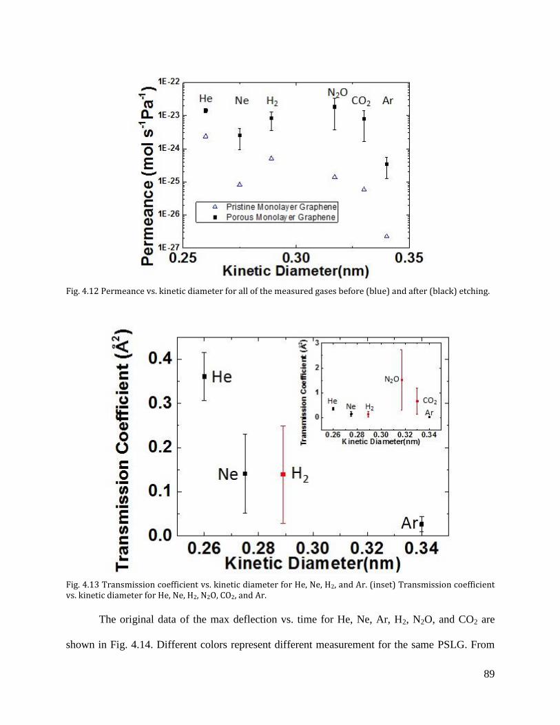
89
Fig. 4.12 Permeance vs. kinetic diameter for all of the measured gases before (blue) and after (black) etching.
Fig. 4.13 Transmission coefficient vs. kinetic diameter for He, Ne, H2, and Ar. (inset) Transmission coefficient vs. kinetic diameter for He, Ne, H2, N2O, CO2, and Ar.
The original data of the max deflection vs. time for He, Ne, Ar, H2, N2O, and CO2 are
shown in Fig. 4.14. Different colors represent different measurement for the same PSLG. From

90
this data, we extracted the leak rate dn/dt vs. pressure difference Δp and the corresponding
permeance.
Fig. 4.14 Maximum Deflection vs time of multiple gases for porous monolayer graphene membrane in Fig. 4.12&4.13.
4.8 Schocastic Switching of Porous Graphene without AuNC
Though the leak rates are relatively constant over long time periods (days) of repeated
measurements, the transmission coefficient demonstrates discretized fluctuations indicative of
stochastic switching. Fig. 4.15a shows the concatenated permeance over time along with a fit to
discrete states using Hidden Markov modeling (see details below). The data in Fig. 4.15a was
taken over the course of five days where a dashed line corresponds to the start of a new
measurement. All measurements are concatenated into a single observed time axis so that the
repetition of certain states and values of permeance can be seen. This switching is clearly seen in
Fig. 4.15b where the permeance switches five times within 1 hour (black circles). The histogram

91
of the permeance for Ne is plotted in Fig. 4.15c. The permeance shows a large number of states
on the low end of the spectrum with occasional switching to faster leak rates. We fit these
permeance values versus time to discrete states and applied a Hidden Markov model (HMM) to
elucidate transition rates 166,167
. The frequency of switching between the states also yields an
approximate value for the activation energy of the switching process, 0.9 eV. This is comparable
to the activation energy required for rearrangement of molecule bonds, such as cis-trans
isomerization.168
These calculations comparing a the model pore and experimental results
demonstrate that relatively minor changes in the pore can have an observable impact on the
permeation characteristics of the pore.
Fig. 4.15 Stochastic switching of the leak rate through porous monolayer graphene without gold nanoparticles (a) Permeance (black circles) and fit (red line) vs. time for all the Ne data. Bottom axis, observable time, corresponds to the 800 minutes of measurements taken over five days after repeated pressurization. Each measurement is separated by a dashed line. (b) Single experimental run within (a) matching highlighted time range. Left axis, blue squares - Maximum deflection versus time for Neon. Right axis– permeance vs. time calculated from the change in deflection vs. time in. (c) Histogram of the permeance for all the data in (a).
For fitting permeance versus time to discrete states, we applied a hidden Markov model
(HMM). HMM describes a system that can switch between various states, however the states are
not directly observable and must be inferred from changes in output. This type of modeling has

92
been applied in fluorescence and sensing applications to model the changes in observed
fluorescence from interactions with an analyte.169
The states and fit were calculated using the
program HaMMy, which was originally developed for HMM analysis of FRET systems.167
The data from multiple runs was analyzed together by concatenating all data sets so that
they have a shared time axis, called observed time. This represents the time in which data was
being measured. The experiments for Ne were done over the course of five days, and the time
between experiments is excluded for the fitting but noted by dashed lines in Fig. 4.15. For
estimating the frequency of transitions between states, the transitions that occurred between the
end of the previous experiment and the start of the next are excluded. Only points and time when
the deflection is above 50 nm are included. When input into the program HaMMy, the
permeance data is normalized by the maximum value, however, after the Markov model fit is
generated, the permeance is converted back to absolute values.
The fitting algorithm fits the data to states that are distinct from each other and treats the
transitions between states as instantaneous. The program was used to fit up to ten states, but it
can also return empty states if the number of recognizable states is lower than ten.
The frequency of transitions between states can be used to estimate the activation energy
of the pore transitions. For Ne, the hidden Markov modeling identified 26 transitions that did not
occur during the time between experimental runs. The total observed time was 785 minutes.
Therefore, the frequency is about 1 transition per 30 minutes, or 2x10⁻³
1/s. The kinetic rate
constant is approximately equivalent to the frequency. For an elementary process, the kinetic
rate constant consists of an attempt frequency, A, and an exponential dependence on activation
energy.
3 12 10aE
RTk Aes
(4-16)

93
Molecular vibrations typically occur within a few orders of magnitude of 1013
1/s.170
We
assume A=1013
, and our data give us k based on one switching in 30minutes. Assuming a
temperature of 298 K, the activation energy for a transition, aE , can be estimated as 0.94 eV.
4.9 Estimation of Change in Permeance from Pore Rearrangement
We attribute the stochastic switching in leak rates to small fluctuations at the pore site
which modulate the transmission probability. One possible source of fluctuations is reaction of
the pore edge functionalization with atmospheric species; another is pore isomerization, in which
the pore transitions between stable chemical states through rearrangement, but no gain or loss, of
the atoms around the pore. Fig. 4.16a illustrates the simplest possible rearrangement: moving a
single carbon atom in a simplified model pore which excludes functionalization. The effective
size is around the expected pore size based on the observed molecular sieving. Even for this
simplified model, this small rearrangement results in a relatively significant change in the energy
barrier, as shown in Fig. 4.16b. That change in the model pore’s estimated energy barrier gives
an expected change in the permeance of around a factor of two or three, which is consistent with
the magnitude of the experimentally observed changes in Fig. 4.15. The sensitivity of the leak
rate to small rearrangements at a single pore further supports the hypothesis that a single pore is
responsible for the observed gas transport in the measured porous graphene.
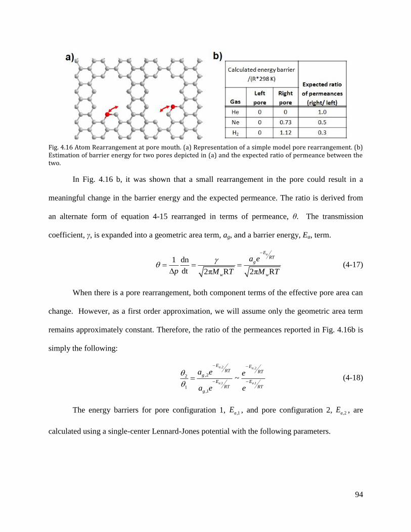
94
Fig. 4.16 Atom Rearrangement at pore mouth. (a) Representation of a simple model pore rearrangement. (b) Estimation of barrier energy for two pores depicted in (a) and the expected ratio of permeance between the two.
In Fig. 4.16 b, it was shown that a small rearrangement in the pore could result in a
meaningful change in the barrier energy and the expected permeance. The ratio is derived from
an alternate form of equation 4-15 rearranged in terms of permeance, θ. The transmission
coefficient, γ, is expanded into a geometric area term, ag, and a barrier energy, Ea, term.
1 dn
dt 2π R 2π R
aERT
g
w w
a e
p M T M T
(4-17)
When there is a pore rearrangement, both component terms of the effective pore area can
change. However, as a first order approximation, we will assume only the geometric area term
remains approximately constant. Therefore, the ratio of the permeances reported in Fig. 4.16b is
simply the following:
,2 ,2
,1 ,1
,22
1,1
~
a a
a a
E ERT RT
g
E E
RT RTg
a e e
a e e
(4-18)
The energy barriers for pore configuration 1, ,1aE , and pore configuration 2, ,2aE , are
calculated using a single-center Lennard-Jones potential with the following parameters.

95
Table 6 Parameters for Lennard-Jones Potential Calculation Center σ (Å) ϵ / kB (K)
C 171 2.960 34.2
Ar 172 3.542 93.3
He 172 2.551 10.22
Ne 172 2.820 32.8
CO2 172 3.941 195.2
H2 172 2.827 59.7
N2 172 3.798 71.4
N2O 172 3.828 232.4
O2 172 3.467 106.7
Fig. 4.16b only includes He, H2, and Ne. The full list of energy barriers is listed below.
Energy barriers that are negative mean that the interaction energy for being in the center of the
pore is more favorable than as a free gas molecule; the energy barrier is treated as zero in this
case. For the larger molecules the energy barrier is larger and means those molecules would
permeate very slowly, effectively blocked relative to the low barrier. CO2 and N2O show large
energy barriers even though experiments show they permeate quickly; as discussed in the
manuscript, this is believed to be the result of favorable electronic interactions that lower the
total interaction energy, which is not captured by the simple Lennard-Jones (L-J) potential.
Table 7 Calculated Energy Barriers L-J Energy barrier
Ea/(R*298)
Gas Fig 4.16a Left
Fig 4.16a Right
He 0 (-0.83) 0 (-0.37)
Ne 0 (-0.96) 0.73
H2 0 (-1.36) 1.12
O2 7.29 23.8
Ar 8.55 25.7
N2 14.5 36.8
CO2 45.5 109.2
N2O 40.9 102.4

96
4.10 Conclusions
In conclusion, we created molecular valves in graphene which allow us to control the gas
flux through a single (nominally) molecular-sized nanopore. The process can be controlled by
movement of AuNC on the graphene surface. These results lead to a greater understanding of
molecular gas transport through molecular-sized pores in atomically-thin materials. The
switching observed may lead to unique sensors based on the reversible switching of molecular
transport through ~atomic size pores reminiscent of ion channels in biological cell membranes,
i. e. sensors for molecules that change configurations, or single molecule binding events.
97
Chapter 5 Ultrathin Oxide Films by Atomic Layer
Deposition on Graphene
5.1 Introduction
Two-dimensional (2D) materials are promising nanomechanical structures.12,29
Graphene,
the best known and studied of this class of materials, boasts a high Young’s modulus, intrinsic
strength, gas impermeability, and excellent thermal and electrical conductivity.7,8,14,18,87
There
are possible applications where flexible ultrathin insulating or oxide films are needed with
comparable mechanical properties. The integration of graphene with other two dimensional (2D)
or quasi-2D materials may also lead to new functional properties for the composite
materials.140,173-176
Currently, the range of ultra-thin materials is severely limited by the materials
and length-scales that are accessible through thin film fabrication.
Mechanical and chemical exfoliation, as well as growth techniques such as chemical
vapor deposition, can produce just a handful of ultra-thin layered materials.23,29,31,177,178
As
traditional materials approach ~ 1 nm film thicknesses, fabrication of freely suspended films is
difficult due to stresses or significant voids in the films that destroy the mechanical integrity of
the film. To overcome these problems, we use suspended graphene membranes as sacrificial
supports to grow high quality ALD films and then remove the graphene to leave the ALD thin
film. These experiments demonstrate that ALD on graphene offers a route to create free-standing,
ultrathin, quasi-2D structures with atomically controlled thickness and mechanical properties
comparable to their bulk counterparts.92,104,179,180

98
5.2 Experimental Methods
Graphene is deposited using mechanical exfoliation over pre-defined etched wells similar
to previously described methods (see Fig. 5.1a).8,29,79
A series of wells with ~5-8 μm diameters
were defined by photolithography on a silicon wafer with 90 nm of thermally grown silicon
oxide. Dry plasma etching (CF4 + O2, followed by SF6) is used to etch wells that are 500 nm – 3
μm and the “scotch tape” method is used to deposit graphene.29
Atomic layer deposition on the graphene is performed in a homebuilt reactor following a
recipe similar to one previously reported for ALD alumina growth on carbon nanotubes.125,139
The samples are placed inside the ALD reactor, pumped down to ~30 mTorr, and held at 180°C
for 30 min - 1 h before beginning the reaction. The reactor is purged with 20 sequences of argon
purging before performing the NO2/TMA nucleation treatment. Each argon purge involved
dosing argon to 1 Torr for 60 s and then pumping for 60 s.
The nucleation treatment involves a dose of NO2 to 1 Torr for 60 s followed by pumping
for 60 s. Subsequently, a dose of TMA to 1 Torr for 60 s is applied, followed by pumping for 60
s. This process is repeated 10 times. After forming this adhesion layer, ALD of alumina is
performed by cycling TMA/H20 doses as follows: dose TMA to 1 Torr for 60 sec, pump for 60
sec, then dose Argon at 20 Torr for 60 sec and pump for 60 seconds 5 times, dose H2O to 1 Torr
for 60 s, pump for 60 s, then dose Argon at 20 Torr for 60 s and pump for 60 s 5 times. This
represents 1 cycle of ALD. After the TMA/H2O cycles are complete, the reactor is purged again
with argon and then the samples are removed. All reactions were performed at 180 (± 0.5) °C.
In summary, atomic layer deposition films are fabricated using a combination of
deposition and etching using a suspended graphene support. The graphene provides an
atomically-smooth growth surface that can easily be etched away. Graphene is mechanically
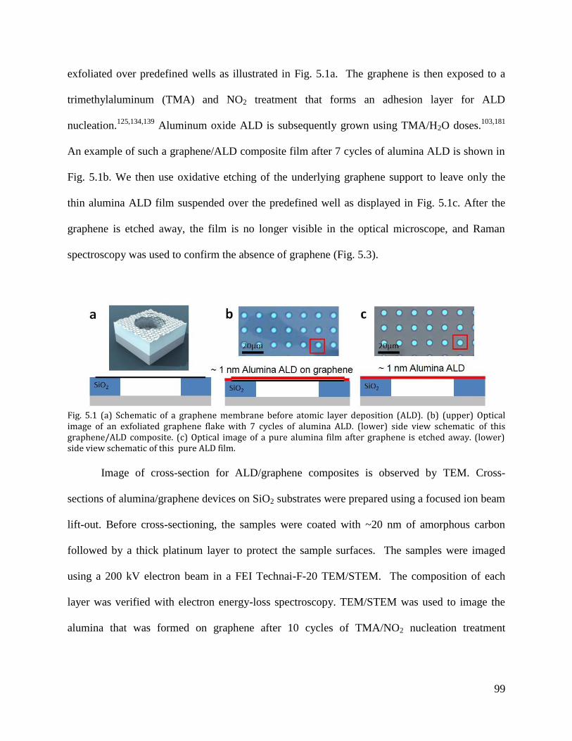
99
exfoliated over predefined wells as illustrated in Fig. 5.1a. The graphene is then exposed to a
trimethylaluminum (TMA) and NO2 treatment that forms an adhesion layer for ALD
nucleation.125,134,139
Aluminum oxide ALD is subsequently grown using TMA/H2O doses.103,181
An example of such a graphene/ALD composite film after 7 cycles of alumina ALD is shown in
Fig. 5.1b. We then use oxidative etching of the underlying graphene support to leave only the
thin alumina ALD film suspended over the predefined well as displayed in Fig. 5.1c. After the
graphene is etched away, the film is no longer visible in the optical microscope, and Raman
spectroscopy was used to confirm the absence of graphene (Fig. 5.3).
Fig. 5.1 (a) Schematic of a graphene membrane before atomic layer deposition (ALD). (b) (upper) Optical image of an exfoliated graphene flake with 7 cycles of alumina ALD. (lower) side view schematic of this graphene/ALD composite. (c) Optical image of a pure alumina film after graphene is etched away. (lower) side view schematic of this pure ALD film.
Image of cross-section for ALD/graphene composites is observed by TEM. Cross-
sections of alumina/graphene devices on SiO2 substrates were prepared using a focused ion beam
lift-out. Before cross-sectioning, the samples were coated with ~20 nm of amorphous carbon
followed by a thick platinum layer to protect the sample surfaces. The samples were imaged
using a 200 kV electron beam in a FEI Technai-F-20 TEM/STEM. The composition of each
layer was verified with electron energy-loss spectroscopy. TEM/STEM was used to image the
alumina that was formed on graphene after 10 cycles of TMA/NO2 nucleation treatment

100
followed by 5 cycles of TMA/H2O ALD deposition. From these images, the observed alumina
layer was amorphous and 2.8 ± 0.3 nm thick.
Fig. 5.2 Bright-field TEM image of a cross-section of supported alumina ALD film on 5-layer graphene supported on silicon oxide. The amorphous alumina layer is 2.8 ± 0.3 nm thick.
Raman spectroscopy was used to confirm the removal of graphene after etching.29
Fig.
5.3 shows Raman spectroscopy of a graphene/ALD composite film before etching of graphene.
The Raman spectrum shows the G and 2D peaks that are characteristic of a bilayer graphene
membrane. After etching, the G and 2D peak are not detectable in the Raman spectrum
confirming that all the graphene was etched away leaving only the suspended pure alumina ALD
film.
Fig. 5.3 (a) Raman spectrum for one of the graphene/ALD composite films in Fig. 3.1b. (b) A representative Raman spectrum on one of the pure alumina ALD films in Fig. 3.1C.

101
5.3 Young’s Modulus of ALD Membranes
We have used blister test to get the Young’s modulus of ALD membranes. A pressure
difference is applied to the film using a previously reported method where slow diffusion
through the SiO2 substrate over-pressurizes the film-sealed microchamber.8,79
An atomic force
microscope (AFM) image of such an over-pressurized suspended film in Fig. 5.1c is shown in
Fig. 5.4a. The ALD film is bulged upward with a maximum deflection through the center of the
film, δ = 261 nm, and a radius, a = 2.76 µm, consistent with the radius of the predefined well. At
increasing Δp, the film stretches further as δ increases as characterized in Fig. 5.4b. During AFM
imaging, the bulge is stable suggesting a constant pressure difference and no significant leak rate
of gas out of the microchamber, similar to previous results on graphene membranes8. This
behavior implies that the aluminum oxide films are pinhole-free and impermeable to the nitrogen
gas used for pressurization.
The deformation of the film follows:79,182
(5-1)
where E is Young’s modulus, t is the thickness of the film, and K(υ) is a constant that depends
on the Poisson’s ratio. For the case of aluminum oxide, K(υ = 0.24) = 3.35.
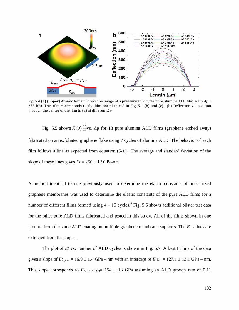
102
Fig. 5.4 (a) (upper) Atomic force microscope image of a pressurized 7 cycle pure alumina ALD film with ∆p = 278 kPa. This film corresponds to the film boxed in red in Fig. 5.1 (b) and (c). (b) Deflection vs. position through the center of the film in (a) at different ∆p.
Fig. 5.5 shows
vs. Δp for 18 pure alumina ALD films (graphene etched away)
fabricated on an exfoliated graphene flake using 7 cycles of alumina ALD. The behavior of each
film follows a line as expected from equation (5-1). The average and standard deviation of the
slope of these lines gives Et = 250 ± 12 GPa-nm.
A method identical to one previously used to determine the elastic constants of pressurized
graphene membranes was used to determine the elastic constants of the pure ALD films for a
number of different films formed using 4 – 15 cycles.8 Fig. 5.6 shows additional blister test data
for the other pure ALD films fabricated and tested in this study. All of the films shown in one
plot are from the same ALD coating on multiple graphene membrane supports. The Et values are
extracted from the slopes.
The plot of Et vs. number of ALD cycles is shown in Fig. 5.7. A best fit line of the data
gives a slope of Etcycle = 16.9 ± 1.4 GPa – nm with an intercept of E0t0 = 127.1 ± 13.1 GPa – nm.
This slope corresponds to EALD Al2O3= 154 ± 13 GPa assuming an ALD growth rate of 0.11
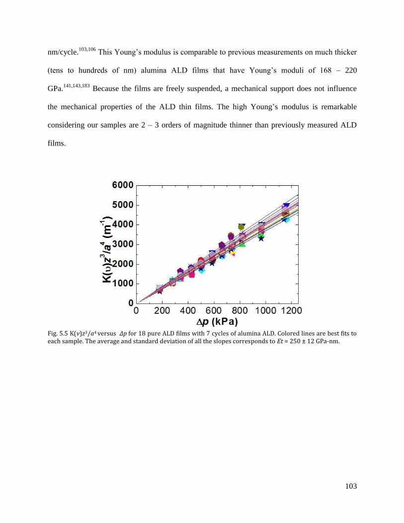
103
nm/cycle.103,106
This Young’s modulus is comparable to previous measurements on much thicker
(tens to hundreds of nm) alumina ALD films that have Young’s moduli of 168 – 220
GPa.141,143,183
Because the films are freely suspended, a mechanical support does not influence
the mechanical properties of the ALD thin films. The high Young’s modulus is remarkable
considering our samples are 2 – 3 orders of magnitude thinner than previously measured ALD
films.
Fig. 5.5 K(ν)z3/a4 versus ∆p for 18 pure ALD films with 7 cycles of alumina ALD. Colored lines are best fits to each sample. The average and standard deviation of all the slopes corresponds to Et = 250 ± 12 GPa-nm.
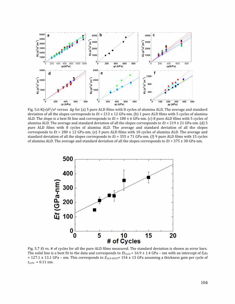
104
Fig. 5.6 K(ν)δ3/a4 versus ∆p for (a) 5 pure ALD films with 8 cycles of alumina ALD. The average and standard deviation of all the slopes corresponds to Et = 213 ± 12 GPa-nm. (b) 1 pure ALD films with 5 cycles of alumina ALD. The slope is a best fit line and corresponds to Et = 180 ± 6 GPa-nm. (c) 8 pure ALD films with 5 cycles of alumina ALD. The average and standard deviation of all the slopes corresponds to Et = 219 ± 21 GPa-nm. (d) 5 pure ALD films with 8 cycles of alumina ALD. The average and standard deviation of all the slopes corresponds to Et = 280 ± 12 GPa-nm. (e) 3 pure ALD films with 10 cycles of alumina ALD. The average and standard deviation of all the slopes corresponds to Et = 355 ± 71 GPa-nm. (f) 9 pure ALD films with 15 cycles of alumina ALD. The average and standard deviation of all the slopes corresponds to Et = 375 ± 38 GPa-nm.
Fig. 5.7 Et vs. # of cycles for all the pure ALD films measured. The standard deviation is shown as error bars. The solid line is a best fit to the data and corresponds to Etcycle = 16.9 ± 1.4 GPa – nm with an intercept of E0t0
= 127.1 ± 13.1 GPa – nm. This corresponds to EALD Al2O3= 154 ± 13 GPa assuming a thickness gain per cycle of tcycle = 0.11 nm.

105
5.4 Mass Density for ALD Membranes
The mass density can be calculated from the resonance method experiments. The
pressure induced-strain in the film can be used to tune the mechanical resonance frequency of the
suspended films. Fig. 5.8 demonstrates this behavior for a graphene/ALD composite film
fabricated using 5 cycles of alumina ALD. The mechanical resonance is actuated and detected
optically as previously reported.8,87
We were unable to measure a resonance frequency for the
pure alumina ALD films presumably due to the lack of optical reflectivity from these samples.
The frequency first decreases and then increases as the film transitions from a bulged upward to
a depressed downward state.
At sufficiently large pressures far from the minimum frequency, the frequency scales as f 3 α Δp.
The slope shows a dramatic decrease in frequency with the addition of alumina ALD cycles as
shown in Fig. 5.9. The pressure inside of the microcavity in Fig. 5.9 is much lower than the
inside pressure in Fig. 5.8, which makes the y-intercept at pext=0 much lower. This behavior can
be explained by the pressure-induced changes in the tension in a stretched circular film according
to:
pa
Etf
A
34
33 )(K107
(5-2)
where ρA is the mass per unit area. From the slope of the lines in Fig. 5.9 and using Et)(K
determined by a pressurized blister test on the composite ALD/graphene film, we can determine
ρA of each suspended film before and after each ALD process. All samples showed an increase in
ρA with number of alumina ALD cycles as displayed in Fig. 5.10a. The first three cycles showed
a larger increase in ρA that may be related to the initial nucleation of alumina ALD. The finite ρA
before any ALD cycles is attributed to the additional mass from the adhesion layer.
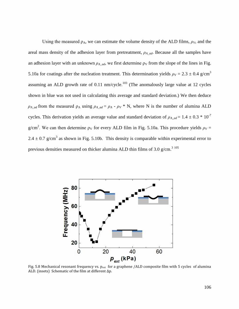
106
Using the measured ρA, we can estimate the volume density of the ALD films, ρV, and the
areal mass density of the adhesion layer from pretreatment, ρA_ad. Because all the samples have
an adhesion layer with an unknown ρA_ad, we first determine ρV from the slope of the lines in Fig.
5.10a for coatings after the nucleation treatment. This determination yields ρV = 2.3 ± 0.4 g/cm3
assuming an ALD growth rate of 0.11 nm/cycle.103
(The anomalously large value at 12 cycles
shown in blue was not used in calculating this average and standard deviation.) We then deduce
ρA_ad from the measured ρA using ρA_ad = ρA - ρV * N, where N is the number of alumina ALD
cycles. This derivation yields an average value and standard deviation of ρA_ad = 1.4 ± 0.3 * 10-7
g/cm2. We can then determine ρV for every ALD film in Fig. 5.10a. This procedure yields ρV =
2.4 ± 0.7 g/cm3 as shown in Fig. 5.10b. This density is comparable within experimental error to
previous densities measured on thicker alumina ALD thin films of 3.0 g/cm.3 105
Fig. 5.8 Mechanical resonant frequency vs. pext for a graphene /ALD composite film with 5 cycles of alumina ALD. (insets) Schematic of the film at different ∆p.

107
Fig. 5.9 Frequency3 vs. pext for a single graphene/ALD composite film with 0, 4, 9, 12 cycles of alumina ALD.
Fig. 5.10 (a) Areal mass density ρA vs. number of cycles for all the graphene/ALD composites measured. (b) Histogram of volume mass density ρV for the alumina ALD films. The black line is a Gaussian fit to the data.
5.5 Initial Tension in Graphene and Graphene/ALD Composite
Films
Even with no applied pressure difference across the films, the frequency of these
nanomechanical resonators still behave as stretched membranes.79
This is illustrated by the high
resonant frequencies exhibited by the membranes even when no pressure difference exists across
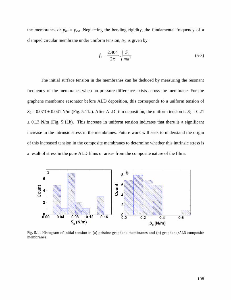
108
the membranes or pint = pext. Neglecting the bending rigidity, the fundamental frequency of a
clamped circular membrane under uniform tension, S0, is given by:
2
00
π2
404.2
ma
Sf (5-3)
The initial surface tension in the membranes can be deduced by measuring the resonant
frequency of the membranes when no pressure difference exists across the membrane. For the
graphene membrane resonator before ALD deposition, this corresponds to a uniform tension of
S0 = 0.073 ± 0.041 N/m (Fig. 5.11a). After ALD film deposition, the uniform tension is S0 = 0.21
± 0.13 N/m (Fig. 5.11b). This increase in uniform tension indicates that there is a significant
increase in the intrinsic stress in the membranes. Future work will seek to understand the origin
of this increased tension in the composite membranes to determine whether this intrinsic stress is
a result of stress in the pure ALD films or arises from the composite nature of the films.
Fig. 5.11 Histogram of initial tension in (a) pristine graphene membranes and (b) graphene/ALD composite membranes.
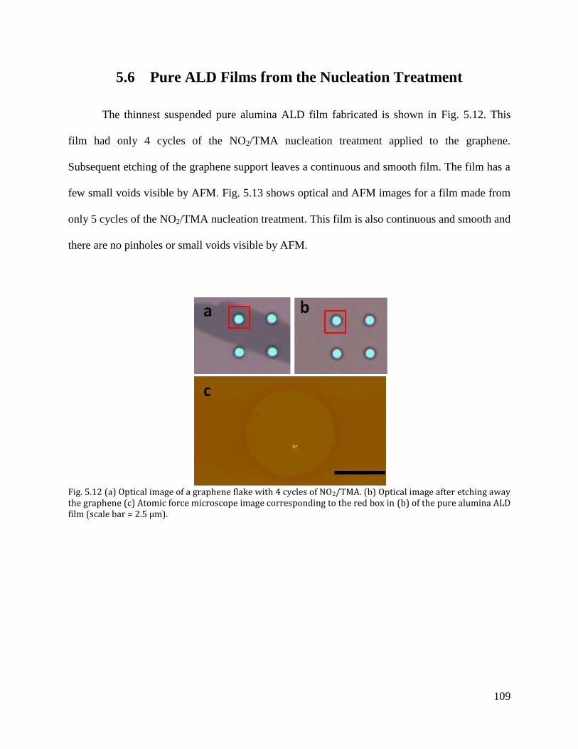
109
5.6 Pure ALD Films from the Nucleation Treatment
The thinnest suspended pure alumina ALD film fabricated is shown in Fig. 5.12. This
film had only 4 cycles of the NO2/TMA nucleation treatment applied to the graphene.
Subsequent etching of the graphene support leaves a continuous and smooth film. The film has a
few small voids visible by AFM. Fig. 5.13 shows optical and AFM images for a film made from
only 5 cycles of the NO2/TMA nucleation treatment. This film is also continuous and smooth and
there are no pinholes or small voids visible by AFM.
Fig. 5.12 (a) Optical image of a graphene flake with 4 cycles of NO2/TMA. (b) Optical image after etching away the graphene (c) Atomic force microscope image corresponding to the red box in (b) of the pure alumina ALD film (scale bar = 2.5 µm).
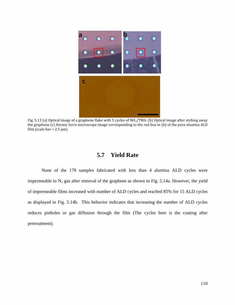
110
Fig. 5.13 (a) Optical image of a graphene flake with 5 cycles of NO2/TMA. (b) Optical image after etching away the graphene (c) Atomic force microscope image corresponding to the red box in (b) of the pure alumina ALD film (scale bar = 2.5 µm).
5.7 Yield Rate
None of the 178 samples fabricated with less than 4 alumina ALD cycles were
impermeable to N2 gas after removal of the graphene as shown in Fig. 5.14a. However, the yield
of impermeable films increased with number of ALD cycles and reached 85% for 15 ALD cycles
as displayed in Fig. 5.14b. This behavior indicates that increasing the number of ALD cycles
reduces pinholes or gas diffusion through the film (The cycles here is the coating after
pretreatment).

111
Fig. 5.14 (a) (black) Number of all pure ALD films fabricated in this study vs. number of ALD coating cycles. (red) Number of pure ALD films that hold N2 gas from that sample batch (b) Percentage yield vs. # of cycles for all the pure ALD films fabricated.
For freely suspended films formed using only 5 cycles of the TMA/NO2 nucleation
treatment, AFM images of the films do not show voids (Fig. 5.13). This corroborates our
measurements of a contribution from the adhesion layer to E and ρA_funct in Fig. 5.7 and Fig. 5.10a.
Future work will examine the dependence of the adhesion layer and its role in nucleating
continuous pinhole-free ALD alumina thin film growth on graphene.

112
5.8 Conclusions
In conclusion, a new class of ultrathin films has been created based on aluminum oxide
ALD on graphene. These films are mechanically robust, pinhole-free, and have ~nm thicknesses
while still maintaining a Young’s modulus comparable to their much thicker counterparts. The
manufacturability, thickness control, and versatility of the ALD process means that materials and
processing can be tailored to suit many applications where traditional silicon or graphene-based
thin film mechanical devices fail to offer the needed functionality.184,185
Furthermore, these films
can be integrated with graphene or other nanomechanical structures to create multifunctional
quasi-2D electromechanical structures.

113
Chapter 6 Summary and Suggestions for Future
Work
6.1 Summary
This thesis summarized a careful study for the gas transport mechanisms of graphene
membrane, which can be used in gas separation. What’s more, it looked into details of
mechanical properties of ultrathin suspended ALD films, which may be used for gas separation.
Chapter 1-3 overviewed the basic concepts and background, which underlie my research; chapter
4-5 provided the results and discussion of the key findings.
Chapter 1 began with fundamentals of graphnene. Then nanopores on graphene was
introduced in detail. Chapter 2 focused on nanomechanics, which started from the solid state
mechanics and dynamics for NEMS. Then it introduced the mechanical properties of graphene in
detail. Chapter 3 gave the basics of ALD and the mechanical properties of Al2O3 ALD.
We created single pore valves from porous graphene membrane to control gas flux in
Chapter 4. In this part, sub-nm pores were introduced to the pristine graphene with UV exposure.
A blister test was used to check the leak rate. Controlling the pore opening and closing using
AuNC dramatically changed gas permeance. We detected the stochastic switching of permeance
on single layer graphene membrane, which is believed to arise from the minor atomic
rearrangements around the pore mouth. The permeance of polar gas molecules were observed to
be much higher than the kinetic theory’s prediction.
Chapter 5 provided a method to fabricate ~nm thin suspended pure ALD Al2O3 films.
ALD Al2O3 was deposited on graphene membranes; then graphene was etched away by
oxidation in furnace at 600°C. No visible voids can be found on ALD films even with just with 5

114
cycles of pretreatment. As the cycles of coating increase, the percentage of membranes, which
can hold gas, increases. From the blister test, we found that the Young’s modulus for ALD Al2O3
is around 154GPa, which is comparable to previous measurements on much thicker alumina
ALD films. From the resonance test, we calculated the mass density is ~2.4 g/cm3, which is
comparable to previous densities measured on thicker alumina ALD thin films.
6.2 Suggestions for Future Work
The preliminary study of single pore on graphene membrane opens a door to a new field.
We can tune the temperature to see the response of the quantized switching. Different
functionalized methods can be tried to modify the permeance switching. Different kinds of nano
blockers can be used on 2D porous materials to create controllable switching. These experiments
can be extended to ion separation, and water desalination too. Besides the experimental work,
systematic analysis may be needed from theorists.
Some in-depth study of ALD ultrathin films is also interesting. AFM nanoindentation can
be used to check its breaking strength. NEMS resonators can be created from pure ALD films.
Blister test or other methods can be used to check its permeance. Since it is easy to scale up with
the uniform coated ALD technique, ALD ultrathin film for gas or ion separation is also attractive.
Moreover, ALD healed porous graphene may lead to some promising results. Recently,
extremely high flux is achieved from porous graphene with high density pore arrays (7.6-nm
pore diameter with 4.0% porosity), but the selectivity is less than 10 for H2/CO2.186
If we can use

115
ALD technique to heal the 7.6nm pore to sub-nm, molecular sieving may be achieved. In this
case, both large flux and high selectivity may be accomplished at the same time.
116
Reference
1 Landau, L. D. Theorie der phasenumwandlungen II. Phys. Z. Sowjetunion 11, 26-35 (1937). 2 Landau, L. D. & Lifshitz, E. M. Statistical Physics, Part I. (1980). 3 Mermin, N. D. Crystalline order in two dimensions. Phys. Rev. 176, 250-254 (1968). 4 Peierls, R. E. Quelques proprietes typiques des corpses solides. Ann. I. H. Poincare 5, 177-222
(1935). 5 Venables, J. A., Spiller, G. D. T. & Hanbucken, M. Nucleation and Growth of Thin-Films. Rep Prog
Phys 47, 399-459, doi:Doi 10.1088/0034-4885/47/4/002 (1984). 6 Novoselov, K. S. et al. Electric field effect in atomically thin carbon films. Science 306, 666-669,
doi:DOI 10.1126/science.1102896 (2004). 7 Lee, C., Wei, X. D., Kysar, J. W. & Hone, J. Measurement of the elastic properties and intrinsic
strength of monolayer graphene. Science 321, 385-388, doi:DOI 10.1126/science.1157996 (2008).
8 Bunch, J. S. et al. Impermeable Atomic Membranes from Graphene Sheets. Nano Letters 8, 2458-2462, doi:10.1021/nl801457b (2008).
9 Jiang, D. E., Cooper, V. R. & Dai, S. Porous Graphene as the Ultimate Membrane for Gas Separation. Nano Lett 9, 4019-4024, doi:Doi 10.1021/Nl9021946 (2009).
10 Stolyarova, E. et al. High-resolution scanning tunneling microscopy imaging of mesoscopic graphene sheets on an insulating surface. Proceedings of the National Academy of Sciences 104, 9209-9212, doi:10.1073/pnas.0703337104 (2007).
11 Novoselov, K. S. Beyond the wonder material. Physics World 22, 27-30 (2009). 12 Geim, A. K. Graphene: Status and Prospects. Science 324, 1530-1534 (2009). 13 Koenig, S. P., Boddeti, N. G., Dunn, M. L. & Bunch, J. S. Ultrastrong adhesion of graphene
membranes. Nat Nano 6, 543-546 (2011). 14 Balandin, A. A. et al. Superior thermal conductivity of single-layer graphene. Nano Letters 8, 902-
907 (2008). 15 Yoon, D., Son, Y. W. & Cheong, H. Negative Thermal Expansion Coefficient of Graphene
Measured by Raman Spectroscopy. Nano Letters 11, 3227-3231, doi:Doi 10.1021/Nl201488g (2011).
16 Novoselov, K. S. et al. Room-temperature quantum hall effect in graphene. Science 315, 1379-1379, doi:DOI 10.1126/science.1137201 (2007).
17 Novoselov, K. S. et al. Two-dimensional gas of massless Dirac fermions in graphene. Nature 438, 197-200, doi:Doi 10.1038/Nature04233 (2005).
18 Zhang, Y., Tan, Y.-W., Stormer, H. L. & Kim, P. Experimental observation of the quantum Hall effect and Berry's phase in graphene. Nature 438, 201-204 (2005).
19 Nair, R. R. et al. Fine structure constant defines visual transparency of graphene. Science 320, 1308-1308, doi:DOI 10.1126/science.1156965 (2008).
20 Riedl, C., Coletti, C., Iwasaki, T., Zakharov, A. A. & Starke, U. Quasi-Free-Standing Epitaxial Graphene on SiC Obtained by Hydrogen Intercalation. Phys Rev Lett 103 (2009).
117
21 Berger, C. et al. Electronic confinement and coherence in patterned epitaxial graphene. Science 312, 1191-1196, doi:DOI 10.1126/science.1125925 (2006).
22 Kim, K. S. et al. Large-scale pattern growth of graphene films for stretchable transparent electrodes. Nature 457, 706-710, doi:Doi 10.1038/Nature07719 (2009).
23 Li, X. S. et al. Large-Area Synthesis of High-Quality and Uniform Graphene Films on Copper Foils. Science 324, 1312-1314, doi:DOI 10.1126/science.1171245 (2009).
24 Li, X. S. et al. Large-Area Graphene Single Crystals Grown by Low-Pressure Chemical Vapor Deposition of Methane on Copper. Journal of the American Chemical Society 133, 2816-2819 (2011).
25 Geim, A. K. & Grigorieva, I. V. Van der Waals heterostructures. Nature 499, 419-425, doi:Doi 10.1038/Nature12385 (2013).
26 Wilson, J. A. & Yoffe, A. D. The transition metal dichalcogenides discussion and interpretation of the observed optical, electrical and structural properties. Advances in Physics 18, 193-335, doi:10.1080/00018736900101307 (1969).
27 Splendiani, A. et al. Emerging Photoluminescence in Monolayer MoS2. Nano Letters 10, 1271-1275, doi:Doi 10.1021/Nl903868w (2010).
28 Mak, K. F., Lee, C., Hone, J., Shan, J. & Heinz, T. F. Atomically Thin MoS2: A New Direct-Gap Semiconductor. Phys Rev Lett 105, doi:Doi 10.1103/Physrevlett.105.136805 (2010).
29 Novoselov, K. S. et al. Two-dimensional atomic crystals. Proceedings of the National Academy of Sciences of the United States of America 102, 10451-10453, doi:DOI 10.1073/pnas.0502848102 (2005).
30 Castellanos-Gomez, A. et al. Laser-Thinning of MoS2: On Demand Generation of a Single-Layer Semiconductor. Nano Letters 12, 3187-3192, doi:Doi 10.1021/Nl301164v (2012).
31 Coleman, J. N. et al. Two-Dimensional Nanosheets Produced by Liquid Exfoliation of Layered Materials. Science 331, 568-571 (2011).
32 Nagashima, A., Tejima, N., Gamou, Y., Kawai, T. & Oshima, C. Electronic Dispersion-Relations of Monolayer Hexagonal Boron-Nitride Formed on the Ni(111) Surface. Phys Rev B 51, 4606-4613, doi:DOI 10.1103/PhysRevB.51.4606 (1995).
33 Novoselov, K. S. & Neto, A. H. C. Two-dimensional crystals-based heterostructures: materials with tailored properties. Phys Scripta T146, doi:Doi 10.1088/0031-8949/2012/T146/014006 (2012).
34 Bonaccorso, F. et al. Production and processing of graphene and 2d crystals. Mater Today 15, 564-589 (2012).
35 Venkatesan, B. M. & Bashir, R. Nanopore sensors for nucleic acid analysis. Nat Nanotechnol 6, 615-624, doi:Doi 10.1038/Nnano.2011.129 (2011).
36 Miles, B. N. et al. Single molecule sensing with solid-state nanopores: novel materials, methods, and applications. Chem Soc Rev 42, 15-28, doi:Doi 10.1039/C2cs35286a (2013).
37 Wanunu, M. et al. Rapid electronic detection of probe-specific microRNAs using thin nanopore sensors. Nat Nanotechnol 5, 807-814, doi:Doi 10.1038/Nnano.2010.202 (2010).
38 Dekker, C. Solid-state nanopores. Nat Nanotechnol 2, 209-215, doi:DOI 10.1038/nnano.2007.27 (2007).
39 Faller, M., Niederweis, M. & Schulz, G. E. The structure of a mycobacterial outer-membrane channel. Science 303, 1189-1192, doi:DOI 10.1126/science.1094114 (2004).
40 Garaj, S. et al. Graphene as a subnanometre trans-electrode membrane. Nature 467, 190-U173, doi:Doi 10.1038/Nature09379 (2010).
41 Hall, J. E. Access Resistance of a Small Circular Pore. J Gen Physiol 66, 531-532, doi:Doi 10.1085/Jgp.66.4.531 (1975).

118
42 Li, J. et al. Ion-beam sculpting at nanometre length scales. Nature 412, 166-169, doi:Doi 10.1038/35084037 (2001).
43 Storm, A. J., Chen, J. H., Ling, X. S., Zandbergen, H. W. & Dekker, C. Fabrication of solid-state nanopores with single-nanometre precision. Nat Mater 2, 537-540, doi:Doi 10.1038/Nmat941 (2003).
44 Merchant, C. A. et al. DNA Translocation through Graphene Nanopores. Nano Lett 10, 2915-2921, doi:Doi 10.1021/Nl101046t (2010).
45 Gierak, J. et al. Sub-5 nm FIB direct patterning of nanodevices. Microelectron Eng 84, 779-783, doi:DOI 10.1016/j.mee.2007.01.059 (2007).
46 Yang, J. J. et al. Rapid and precise scanning helium ion microscope milling of solid-state nanopores for biomolecule detection. Nanotechnology 22, doi:Doi 10.1088/0957-4484/22/28/285310 (2011).
47 Ayub, M. et al. Precise electrochemical fabrication of sub-20 nm solid-state nanopores for single-molecule biosensing. J Phys-Condens Mat 22, doi:Doi 10.1088/0953-8984/22/45/454128 (2010).
48 Nilsson, J., Lee, J. R. I., Ratto, T. V. & Letant, S. E. Localized functionalization of single nanopores. Adv Mater 18, 427-+, doi:DOI 10.1002/adma.200501991 (2006).
49 Danelon, C., Santschi, C., Brugger, J. & Vogel, H. Fabrication and functionalization of nanochannels by electron-beam-induced silicon oxide deposition. Langmuir 22, 10711-10715, doi:Doi 10.1021/La061321c (2006).
50 Koenig, S. P., Wang, L. D., Pellegrino, J. & Bunch, J. S. Selective molecular sieving through porous graphene. Nat Nanotechnol 7, 728-732, doi:Doi 10.1038/Nnano.2012.162 (2012).
51 Maxwell–Boltzmann distribution, <http://en.wikipedia.org/wiki/Maxwell%E2%80%93Boltzmann_distribution> (
52 Reif, F. Fundamentals of Statistical and Thermal Physics. (McGraw-Hill Inc., 1965). 53 Gombosi, T. I. Gaskinetic theory. (Cambridge Unversity Press, 1994). 54 Baker, R. W. Membrane Technology and Applications. (John Wiley & Sons Ltd, 2004). 55 Behling, R. D., Ohlrogge, K., Peinemann, K.-V. & Kyburz, E. The Separation of Hydrocarbons from
Waste Vapor Streams. (1989). 56 Pandey, P. & Chauhan, R. S. Membranes for gas separation. Prog Polym Sci 26, 853-893, doi:Doi
10.1016/S0079-6700(01)00009-0 (2001). 57 Barrer, R. M. Diffusion in Porous Media. Appl. Mater. Res. 2 (1963). 58 Hassan, M. H., Way, J. D., Thoen, P. M. & Dillon, A. C. Single-Component and Mixed-Gas
Transport in a Silica Hollow-Fiber Membrane. J Membrane Sci 104, 27-42, doi:Doi 10.1016/0376-7388(95)00009-2 (1995).
59 Keizer, K., Burggraaf, A. J., Vroon, Z. A. E. P. & Verweij, H. Two component permeation through thin zeolite MFI membranes. J Membrane Sci 147, 159-172, doi:Doi 10.1016/S0376-7388(98)00133-1 (1998).
60 Ash, R., Barrer, R. M. & Pope, C. G. Flow of Adsorbable Gases and Vapours in a Microporous Medium .2. Binary Mixtures. Proc R Soc Lon Ser-A 271, 19-+, doi:DOI 10.1098/rspa.1963.0002 (1963).
61 Drahushuk, L. W. & Strano, M. S. Mechanisms of Gas Permeation through Single Layer Graphene Membranes. Langmuir 28, 16671-16678, doi:Doi 10.1021/La303468r (2012).
62 Liu, H., Chen, Z., Dai, S. & Jiang, D.-e. Selectivity trend of gas separation through nanoporous graphene. Journal of Solid State Chemistry, doi:http://dx.doi.org/10.1016/j.jssc.2014.01.030 (2014).
63 Sun, C. et al. Mechanisms of Molecular Permeation through Nanoporous Graphene Membranes. Langmuir 30, 675-682, doi:10.1021/la403969g (2013).

119
64 Plimpton, S. Fast Parallel Algorithms for Short-Range Molecular-Dynamics. J Comput Phys 117, 1-19, doi:DOI 10.1006/jcph.1995.1039 (1995).
65 Bonomi, M. et al. PLUMED: A portable plugin for free-energy calculations with molecular dynamics. Comput Phys Commun 180, 1961-1972, doi:DOI 10.1016/j.cpc.2009.05.011 (2009).
66 Girit, C. O. et al. Graphene at the Edge: Stability and Dynamics. Science 323, 1705-1708, doi:DOI 10.1126/science.1166999 (2009).
67 Zan, R., Bangert, U., Ramasse, Q. & Novoselov, K. S. Metal-Graphene Interaction Studied via Atomic Resolution Scanning Transmission Electron Microscopy. Nano Lett 11, 1087-1092, doi:Doi 10.1021/Nl103980h (2011).
68 Amft, M., Sanyal, B., Eriksson, O. & Skorodumova, N. V. Small gold clusters on graphene, their mobility and clustering: a DFT study. J Phys-Condens Mat 23, doi:Doi 10.1088/0953-8984/23/20/205301 (2011).
69 Hardcastle, T. P. et al. Mobile metal adatoms on single layer, bilayer, and trilayer graphene: An ab initio DFT study with van der Waals corrections correlated with electron microscopy data. Phys Rev B 87, doi:Doi 10.1103/Physrevb.87.195430 (2013).
70 Liu, L. et al. Slow Gold Adatom Diffusion on Graphene: Effect of Silicon Dioxide and Hexagonal Boron Nitride Substrates. J Phys Chem B 117, 4305-4312, doi:Doi 10.1021/Jp305521g (2013).
71 Wang, H. T. et al. Interaction between single gold atom and the graphene edge: A study via aberration-corrected transmission electron microscopy. Nanoscale 4, 2920-2925, doi:Doi 10.1039/C2nr00059h (2012).
72 Roukes, M. Nanoelectromechanical systems face the future. Physics World 14, 25-31 (2001). 73 Naik, A. K., Hanay, M. S., Hiebert, W. K., Feng, X. L. & Roukes, M. L. Towards single-molecule
nanomechanical mass spectrometry. Nat Nanotechnol 4, 445-450, doi:Doi 10.1038/Nnano.2009.152 (2009).
74 Yang, Y. T., Callegari, C., Feng, X. L. & Roukes, M. L. Surface Adsorbate Fluctuations and Noise in Nanoelectromechanical Systems. Nano Letters 11, 1753-1759, doi:Doi 10.1021/Nl2003158 (2011).
75 Jensen, K., Kim, K. & Zettl, A. An atomic-resolution nanomechanical mass sensor. Nat Nanotechnol 3, 533-537, doi:DOI 10.1038/nnano.2008.200 (2008).
76 Fung, Y. C. & Tong, P. Classical and Computational Solid Mechanics. (World Scientific Publishing Co. Pte. Ltd., 2001).
77 Nix, W. D. Lecture Notes for "Mechanical Properties of Thin Films". (2005). 78 Hencky, H. Uber den spannungzustand in kreisrunden platten mit verschwindender
biegungssteiflgeit. Z. fur Mathematik und Physik 63, 311-317 (1915). 79 Koenig, S. P., Boddeti, N. G., Dunn, M. L. & Bunch, J. S. Ultrastrong adhesion of graphene
membranes. Nat Nanotechnol 6, 543-546 (2011). 80 King, G. C. Vibrations and Waves. (John Wiley & Sons Ltd, 2009). 81 Huang, X. M. H., Feng, X. L., Zorman, C. A., Mehregany, M. & Roukes, M. L. VHF, UHF and
microwave frequency nanomechanical resonators. New J Phys 7 (2005). 82 Timoshenko, S., Young, D. H. & Weaver, W. Vibration Problems in Engineering. (John Wiley &
Sons, Inc., 1974). 83 Chiu, H. Y., Hung, P., Postma, H. W. C. & Bockrath, M. Atomic-Scale Mass Sensing Using Carbon
Nanotube Resonators. Nano Letters 8, 4342-4346, doi:Doi 10.1021/Nl802181c (2008). 84 Hagedorn, P. & DasGupta, A. Vibrations and Waves in Continuous Mechanical Systems. (John
Wiley & Sons Ltd, 2007). 85 Arlett, J. L., Myers, E. B. & Roukes, M. L. Comparative advantages of mechanical biosensors. Nat
Nanotechnol 6, 203-215, doi:DOI 10.1038/nnano.2011.44 (2011).

120
86 Barton, R. A. et al. High, Size-Dependent Quality Factor in an Array of Graphene Mechanical Resonators. Nano Lett 11, 1232-1236, doi:Doi 10.1021/Nl1042227 (2011).
87 Bunch, J. S. et al. Electromechanical resonators from graphene sheets. Science 315, 490-493, doi:DOI 10.1126/science.1136836 (2007).
88 van der Zande, A. M. et al. Large-Scale Arrays of Single-Layer Graphene Resonators. Nano Lett 10, 4869-4873, doi:Doi 10.1021/Nl102713c (2010).
89 Saleh, B. E. A. & Teich, M. C. Fundamentals of Photonics. (John Wiley & Sons, Inc., 2007). 90 Bunch, J. S. Mechanical and Electrical Properties of Graphene Sheets ph. D. thesis, Cornell
University, (2008). 91 Bunch, J. S. Mechanical and electrical properties of graphene sheets Ph.D thesis, Cornell
University, (2008). 92 Ritala, M. et al. Perfectly conformal TiN and Al2O3 films deposited by atomic layer deposition.
Chem Vapor Depos 5, 7-9, doi:Doi 10.1002/(Sici)1521-3862(199901)5:1<7::Aid-Cvde7>3.0.Co;2-J (1999).
93 Paranjpe, A., Gopinath, S., Omstead, T. & Bubber, R. Atomic layer deposition of AlOx for thin film head gap applications. Journal of the Electrochemical Society 148, G465-G471, doi:Doi 10.1149/1.1385822 (2001).
94 Chatham, H. Oxygen diffusion barrier properties of transparent oxide coatings on polymeric substrates. Surf Coat Tech 78, 1-9 (1996).
95 George, S. M. Atomic Layer Deposition: An Overview. Chem Rev 110, 111-131, doi:Doi 10.1021/Cr900056b (2010).
96 Miikkulainen, V., Leskela, M., Ritala, M. & Puurunen, R. L. Crystallinity of inorganic films grown by atomic layer deposition: Overview and general trends. J Appl Phys 113, doi:Doi 10.1063/1.4757907 (2013).
97 Puurunen, R. L. Surface chemistry of atomic layer deposition: A case study for the trimethylaluminum/water process. J Appl Phys 97, doi:Doi 10.1063/1.1940727 (2005).
98 Puurunen, R. L. Growth per cycle in atomic layer deposition: A theoretical model. Chem Vapor Depos 9, 249-257, doi:DOI 10.1002/cvde.200306265 (2003).
99 Higashi, G. S. & Fleming, C. G. Sequential Surface Chemical-Reaction Limited Growth of High-Quality Al2o3 Dielectrics. Appl Phys Lett 55, 1963-1965, doi:Doi 10.1063/1.102337 (1989).
100 Soto, C. & Tysoe, W. T. The Reaction Pathway for the Growth of Alumina on High Surface-Area Alumina and in Ultrahigh-Vacuum by a Reaction between Trimethyl Aluminum and Water. J Vac Sci Technol A 9, 2686-2695 (1991).
101 Goldstein, D. N., McCormick, J. A. & George, S. M. Al(2)O(3) Atomic Layer Deposition with Trimethylaluminum and Ozone Studied by in Situ Transmission FTIR Spectroscopy and Quadrupole Mass Spectrometry. J Phys Chem C 112, 19530-19539, doi:Doi 10.1021/Jp804296a (2008).
102 Kim, J. B. et al. Improvement in Al2O3 dielectric behavior by using ozone as an oxidant for the atomic layer deposition technique. Journal of Applied Physics 92, 6739-6742 (2002).
103 Ott, A. W., Klaus, J. W., Johnson, J. M. & George, S. M. Al3O3 thin film growth on Si(100) using binary reaction sequence chemistry. Thin Solid Films 292, 135-144, doi:Doi 10.1016/S0040-6090(96)08934-1 (1997).
104 Elam, J. W., Groner, M. D. & George, S. M. Viscous flow reactor with quartz crystal microbalance for thin film growth by atomic layer deposition. Review of Scientific Instruments 73, 2981-2987 (2002).
105 Groner, M. D., Fabreguette, F. H., Elam, J. W. & George, S. M. Low-temperature Al2O3 atomic layer deposition. Chemistry of Materials 16, 639-645 (2004).

121
106 Ott, A. W., McCarley, K. C., Klaus, J. W., Way, J. D. & George, S. M. Atomic layer controlled deposition of Al2O3 films using binary reaction sequence chemistry. Appl Surf Sci 107, 128-136, doi:Doi 10.1016/S0169-4332(96)00503-X (1996).
107 Groner, M. D., Elam, J. W., Fabreguette, F. H. & George, S. M. Electrical characterization of thin Al2O3 films grown by atomic layer deposition on silicon and various metal substrates. Thin Solid Films 413, 186-197, doi:Doi 10.1016/S0040-6090(02)00438-8 (2002).
108 Jensen, J. M. et al. X-ray reflectivity characterization of ZnO/Al2O3 multilayers prepared by atomic layer deposition. Chem Mater 14, 2276-2282, doi:Doi 10.1021/Cm011587z (2002).
109 Kuse, R., Kundu, M., Yasuda, T., Miyata, N. & Toriumi, A. Effect of precursor concentration in atomic layer deposition of Al2O3. J Appl Phys 94, 6411-6416, doi:Doi 10.1063/1.1618918 (2003).
110 Matero, R., Rahtu, A., Ritala, M., Leskela, M. & Sajavaara, T. Effect of water dose on the atomic layer deposition rate of oxide thin films. Thin Solid Films 368, 1-7, doi:Doi 10.1016/S0040-6090(00)00890-7 (2000).
111 Puurunen, R. L. et al. Island growth in the atomic layer deposition of zirconium oxide and aluminum oxide on hydrogen-terminated silicon: Growth mode modeling and transmission electron microscopy. J Appl Phys 96, 4878-4889, doi:Doi 10.1063/1.1787624 (2004).
112 Sneh, O., Clark-Phelps, R. B., Londergan, A. R., Winkler, J. & Seidel, T. E. Thin film atomic layer deposition equipment for semiconductor processing. Thin Solid Films 402, 248-261, doi:Doi 10.1016/S0040-6090(01)01678-9 (2002).
113 Yun, S. J., Lee, K. H., Skarp, J., Kim, H. R. & Nam, K. S. Dependence of atomic layer-deposited Al2O3 films characteristics on growth temperature and Al precursors of Al(CH3)(3) and AlCl3. J Vac Sci Technol A 15, 2993-2997, doi:Doi 10.1116/1.580895 (1997).
114 Nishizawa, J., Abe, H. & Kurabayashi, T. Molecular Layer Epitaxy. Journal of the Electrochemical Society 132, 1197-1200, doi:Doi 10.1149/1.2114058 (1985).
115 Sneh, O., Wise, M. L., Ott, A. W., Okada, L. A. & George, S. M. Atomic Layer Growth of Sio2 on Si(100) Using Sicl4 and H2o in a Binary Reaction Sequence. Surface Science 334, 135-152 (1995).
116 Skarp, J. I., Soininen, P. J. & Soininen, P. T. ALE-reactor for large area depositions. Applied Surface Science 112, 251-254, doi:Doi 10.1016/S0169-4332(96)01000-8 (1997).
117 Robertson, J. High dielectric constant oxides. Eur Phys J-Appl Phys 28, 265-291, doi:DOI 10.1051/epjap:2004206 (2004).
118 Kong, J. et al. Nanotube molecular wires as chemical sensors. Science 287, 622-625, doi:DOI 10.1126/science.287.5453.622 (2000).
119 Martel, R., Schmidt, T., Shea, H. R., Hertel, T. & Avouris, P. Single- and multi-wall carbon nanotube field-effect transistors. Appl Phys Lett 73, 2447-2449, doi:Doi 10.1063/1.122477 (1998).
120 Garces, N. Y. et al. Epitaxial graphene surface preparation for atomic layer deposition of Al2O3. J Appl Phys 109, doi:Doi 10.1063/1.3596761 (2011).
121 Ng, H. T. et al. Single crystal nanowire vertical surround-gate field-effect transistor. Nano Lett 4, 1247-1252, doi:Doi 10.1021/Nl049461z (2004).
122 Peng, H. B. & Golovchenko, J. A. Coulomb blockade in suspended Si3N4-coated single-walledcarbon nanotubes. Appl Phys Lett 84, 5428-5430, doi:doi:http://dx.doi.org/10.1063/1.1765733 (2004).
123 Deheer, W. A., Chatelain, A. & Ugarte, D. A Carbon Nanotube Field-Emission Electron Source. Science 270, 1179-1180, doi:DOI 10.1126/science.270.5239.1179 (1995).
124 Dai, H. J., Hafner, J. H., Rinzler, A. G., Colbert, D. T. & Smalley, R. E. Nanotubes as nanoprobes in scanning probe microscopy. Nature 384, 147-150, doi:Doi 10.1038/384147a0 (1996).
122
125 Cavanagh, A. S., Wilson, C. A., Weimer, A. W. & George, S. M. Atomic layer deposition on gram quantities of multi-walled carbon nanotubes. Nanotechnology 20, doi:Doi 10.1088/0957-4484/20/25/255602 (2009).
126 Farmer, D. B. & Gordon, R. G. ALD of high-kappa dielectrics on suspended functionalized SWNTs. Electrochem Solid St 8, G89-G91, doi:Doi 10.1149/1.1862474 (2005).
127 Xuan, Y. et al. Atomic-layer-deposited nanostructures for graphene-based nanoelectronics. Appl Phys Lett 92 (2008).
128 Fallahazad, B., Kim, S., Colombo, L. & Tutuc, E. Dielectric thickness dependence of carrier mobility in graphene with HfO2 top dielectric. Appl Phys Lett 97, doi:Doi 10.1063/1.3492843 (2010).
129 Farmer, D. B. et al. Utilization of a Buffered Dielectric to Achieve High Field-Effect Carrier Mobility in Graphene Transistors. Nano Lett 9, 4474-4478, doi:Doi 10.1021/Nl902788u (2009).
130 Kim, S. et al. Realization of a high mobility dual-gated graphene field-effect transistor with Al2O3 dielectric. Appl Phys Lett 94, doi:Doi 10.1063/1.3077021 (2009).
131 Meric, I. et al. Channel Length Scaling in Graphene Field-Effect Transistors Studied with Pulsed Current-Voltage Measurements. Nano Lett 11, 1093-1097, doi:Doi 10.1021/Nl103993z (2011).
132 Pirkle, A., Wallace, R. M. & Colombo, L. In situ studies of Al2O3 and HfO2 dielectrics on graphite. Appl Phys Lett 95, doi:Doi 10.1063/1.3238560 (2009).
133 Robinson, J. A. et al. Epitaxial Graphene Materials Integration: Effects of Dielectric Overlayers on Structural and Electronic Properties. Acs Nano 4, 2667-2672, doi:Doi 10.1021/Nn1003138 (2010).
134 Wang, X. R., Tabakman, S. M. & Dai, H. J. Atomic layer deposition of metal oxides on pristine and functionalized graphene. J Am Chem Soc 130, 8152-+, doi:Doi 10.1021/Ja8023059 (2008).
135 Yamaguchi, T., Masubuchi, S., Iguchi, K., Moriya, R. & Machida, T. Tunnel spin injection into graphene using Al2O3 barrier grown by atomic layer deposition on functionalized graphene surface. J Magn Magn Mater 324, 849-852, doi:DOI 10.1016/j.jmmm.2011.09.031 (2012).
136 Lee, B. K. et al. Conformal Al2O3 dielectric layer deposited by atomic layer deposition for graphene-based nanoelectronics. Appl Phys Lett 92, doi:Doi 10.1063/1.2928228 (2008).
137 Shin, Y. J. et al. Surface-Energy Engineering of Graphene. Langmuir 26, 3798-3802, doi:Doi 10.1021/La100231u (2010).
138 Dlubak, B., Kidambi, P. R., Weatherup, R. S., Hofmann, S. & Robertson, J. Substrate-assisted nucleation of ultra-thin dielectric layers on graphene by atomic layer deposition. Appl Phys Lett 100, doi:Doi 10.1063/1.4707376 (2012).
139 Farmer, D. B. & Gordon, R. G. Atomic layer deposition on suspended single-walled carbon nanotubes via gas-phase noncovalent functionalization. Nano Lett 6, 699-703, doi:Doi 10.1021/Nl052453d (2006).
140 Williams, J. R., DiCarlo, L. & Marcus, C. M. Quantum hall effect in a gate-controlled p-n junction of graphene. Science 317, 638-641, doi:DOI 10.1126/science.1144657 (2007).
141 Miller, D. C. et al. Thermo-mechanical properties of alumina films created using the atomic layer deposition technique. Sensors and Actuators a-Physical 164, 58-67 (2010).
142 Small, M. K. & Nix, W. D. Analysis of the Accuracy of the Bulge Test in Determining the Mechanical-Properties of Thin-Films. J Mater Res 7, 1553-1563, doi:Doi 10.1557/Jmr.1992.1553 (1992).
143 Tripp, M. K. et al. The mechanical properties of atomic layer deposited alumina for use in micro- and nano-electromechanical systems. Sensor Actuat a-Phys 130, 419-429, doi:DOI 10.1016/j.sna.2006.01.029 (2006).
144 Cleland, A. N. Foundations of Nanomechanics. (Springer, 2003). 145 Ilic, B., Krylov, S. & Craighead, H. G. Young's modulus and density measurements of thin atomic
layer deposited films using resonant nanomechanics. Journal of Applied Physics 108 (2010).
123
146 Ahn, J. Y., Chung, W. J., Pinnau, I. & Guiver, M. D. Poly sulfone/silica nanoparticle mixed-matrix membranes for gas separation. J Membrane Sci 314, 123-133, doi:DOI 10.1016/j.memsci.2008.01.031 (2008).
147 de Vos, R. M. & Verweij, H. High-selectivity, high-flux silica membranes for gas separation. Science 279, 1710-1711, doi:DOI 10.1126/science.279.5357.1710 (1998).
148 Fuertes, A. B. & Centeno, T. A. Carbon molecular sieve membranes from polyetherimide. Micropor Mesopor Mat 26, 23-26, doi:Doi 10.1016/S1387-1811(98)00204-2 (1998).
149 Jiang, L. Y., Chung, T. S., Cao, C., Huang, Z. & Kulprathipanja, S. Fundamental understanding of nano-sized zeolite distribution in the formation of the mixed matrix single- and dual-layer asymmetric hollow fiber membranes. J Membrane Sci 252, 89-100, doi:DOI 10.1016/j.memsci.2004.12.004 (2005).
150 Kim, Y. K., Park, H. B. & Lee, Y. M. Carbon molecular sieve membranes derived from thermally labile polymer containing blend polymers and their gas separation properties. J Membrane Sci 243, 9-17, doi:DOI 10.1016/j.memsci.2004.05.001 (2004).
151 Lai, Z. P. et al. Microstructural optimization of a zeolite membrane for organic vapor separation. Science 300, 456-460, doi:DOI 10.1126/science.1082169 (2003).
152 Liu, S. M. & Gavalas, G. R. Oxygen selective ceramic hollow fiber membranes. J Membrane Sci 246, 103-108, doi:DOI 10.1016/j.memsci.2004.09.028 (2005).
153 Park, H. B. et al. Polymers with cavities tuned for fast selective transport of small molecules and ions. Science 318, 254-258, doi:DOI 10.1126/science.1146744 (2007).
154 Shiflett, M. B. & Foley, H. C. Ultrasonic deposition of high-selectivity nanoporous carbon membranes. Science 285, 1902-1905, doi:DOI 10.1126/science.285.5435.1902 (1999).
155 Strathmann, H. Membrane separation processes: Current relevance and future opportunities. Aiche J 47, 1077-1087, doi:DOI 10.1002/aic.690470514 (2001).
156 Hinds, B. J. et al. Aligned multiwalled carbon nanotube membranes. Science 303, 62-65, doi:DOI 10.1126/science.1092048 (2004).
157 Boutilier, M. S. H. et al. Implications of Permeation through Intrinsic Defects in Graphene on the Design of Defect-Tolerant Membranes for Gas Separation. Acs Nano 8, 841-849, doi:10.1021/nn405537u (2014).
158 Joshi, R. K. et al. Precise and ultrafast molecular sieving through graphene oxide membranes. arXiv:1401.3134 (2014).
159 Kim, H. W. et al. Selective Gas Transport Through Few-Layered Graphene and Graphene Oxide Membranes. Science 342, 91-95, doi:DOI 10.1126/science.1236098 (2013).
160 Li, H. et al. Ultrathin, Molecular-Sieving Graphene Oxide Membranes for Selective Hydrogen Separation. Science 342, 95-98, doi:DOI 10.1126/science.1236686 (2013).
161 Liu, H., Dai, S. & Jiang, D.-e. Insights into CO2/N2 separation through nanoporous graphene from molecular dynamics. Nanoscale 5, 9984-9987, doi:10.1039/c3nr02852f (2013).
162 Mehio, N., Dai, S. & Jiang, D.-e. Quantum Mechanical Basis for Kinetic Diameters of Small Gaseous Molecules. The Journal of Physical Chemistry A, doi:10.1021/jp412588f (2014).
163 Shan, M. et al. Influence of chemical functionalization on the CO2/N2 separation performance of porous graphene membranes. Nanoscale 4, 5477-5482, doi:10.1039/c2nr31402a (2012).
164 Nair, R. R., Wu, H. A., Jayaram, P. N., Grigorieva, I. V. & Geim, A. K. Unimpeded Permeation of Water Through Helium-Leak-Tight Graphene-Based Membranes. Science 335, 442-444, doi:DOI 10.1126/science.1211694 (2012).
165 Wang, L. D. et al. Ultrathin Oxide Films by Atomic Layer Deposition on Graphene. Nano Letters 12, 3706-3710, doi:Doi 10.1021/Nl3014956 (2012).

124
166 Jin, H., Heller, D. A., Kim, J. H. & Strano, M. S. Stochastic Analysis of Stepwise Fluorescence Quenching Reactions on Single-Walled Carbon Nanotubes: Single Molecule Sensors. Nano Lett 8, 4299-4304, doi:Doi 10.1021/Nl802010z (2008).
167 McKinney, S. A., Joo, C. & Ha, T. Analysis of single-molecule FRET trajectories using hidden Markov modeling. Biophys J 91, 1941-1951 (2006).
168 Cembran, A., Bernardi, F., Garavelli, M., Gagliardi, L. & Orlandi, G. On the Mechanism of the cis−trans Isomerization in the Lowest Electronic States of Azobenzene: S0, S1, and T1. J Am Chem Soc 126, 3234-3243, doi:10.1021/ja038327y (2004).
169 Jin, H., Heller, D. A., Kim, J.-H. & Strano, M. S. Stochastic Analysis of Stepwise Fluorescence Quenching Reactions on Single-Walled Carbon Nanotubes: Single Molecule Sensors. Nano letters 8, 4299-4304, doi:10.1021/nl802010z (2008).
170 Kolasinki, K. W. Surface Science: Foundations of Catalysis and Nanoscience. (Wiley, 2008). 171 Steele, W. A. The Interaction of Gases with Solid Surfaces. (Pergamon Press, 1974). 172 Reid, R. C., Prausnitz, J. M. & Poling, B. E. The Properties of Gases and Liquids. (McGraw-Hill,
1987). 173 Dean, C. R. et al. Boron nitride substrates for high-quality graphene electronics. Nat Nano 5,
722-726 (2010). 174 Huang, P. Y. et al. Direct Imaging of a Two-Dimensional Silica Glass on Graphene. Nano Letters
12, 1081-1086 (2012). 175 Jen, S. H., Bertrand, J. A. & George, S. M. Critical tensile and compressive strains for cracking of
Al(2)O(3) films grown by atomic layer deposition. Journal of Applied Physics 109 (2011). 176 Rogers, J. A., Lagally, M. G. & Nuzzo, R. G. Synthesis, assembly and applications of
semiconductor nanomembranes. Nature 477, 45-53 (2011). 177 Suk, J. W., Murali, S., An, J. & Ruoff, R. S. Mechanical measurements of ultra-thin amorphous
carbon membranes using scanning atomic force microscopy. Carbon 50, 2220-2225 (2012). 178 Zhan, Y., Liu, Z., Najmaei, S., Ajayan, P. M. & Lou, J. Large-Area Vapor-Phase Growth and
Characterization of MoS2 Atomic Layers on a SiO2 Substrate. Small 8, 966-971. 179 Leskela, M. & Ritala, M. Atomic layer deposition (ALD): from precursors to thin film structures.
Thin Solid Films 409, 138-146 (2002). 180 Leskela, M. & Ritala, M. Atomic layer deposition chemistry: Recent developments and future
challenges. Angewandte Chemie-International Edition 42, 5548-5554 (2003). 181 Dillon, A. C., Ott, A. W., Way, J. D. & George, S. M. Surface-Chemistry of Al2O3 Deposition Using
Al(Ch3)(3) and H2O in a Binary Reaction Sequence. Surface Science 322, 230-242 (1995). 182 Hencky, H. Uber den spannungszustand in kreisrunden platten mit verschwindender
biegungssteiflgkeit. Zeitschrift fur Mathematik und Physik 63, 311-317 (1915). 183 Tapily, K. et al. Nanoindentation investigation of HfO(2) and Al(2)O(3) films grown by atomic
layer deposition. Journal of the Electrochemical Society 155, H545-H551 (2008). 184 Davidson, B. D., Seghete, D., George, S. M. & Bright, V. M. ALD tungsten NEMS switches and
tunneling devices. Sensors and Actuators a-Physical 166, 269-276 (2011). 185 Yoneoka, S. et al. Electrical and Thermal Conduction in Atomic Layer Deposition Nanobridges
Down to 7 nm Thickness. Nano Letters 12, 683-686, doi:10.1021/nl203548w (2012). 186 Celebi, K. et al. Ultimate Permeation Across Atomically Thin Porous Graphene. Science 344, 289-
292, doi:DOI 10.1126/science.1249097 (2014).