graphene2014 poster book v.2
DESCRIPTION
On behalf of the Organising, Scientific and Local Committees we take great pleasure in welcoming you to Toulouse for the fourth edition of the Graphene International Conference & Exhibition. A plenary session with internationally renowned speakers, extensive thematic workshops in parallel, one-to-one meetings (Brokerage Event) and a significant industrial exhibition featuring current and future Graphene developments will be highlighted at the event. Graphene 2014 is now an established event, attracting global participants intent on sharing, exchanging and exploring new avenues of graphene-related scientific and commercial developments. The event is raising great interest and is now considered as the Graphene meeting point in 2014. We truly hope that Graphene 2014 serves as an international platform for communication between science and business.TRANSCRIPT

Poster Book Vol. 2

Graphene2014 May 06-09, 2014 Toulouse (France)
OREWORD
On behalf of the Organising, Scientific and Local Committees we take great pleasure in welcoming you to Toulouse for the fourth edition of the Graphene International Conference & Exhibition.
A plenary session with internationally renowned speakers, extensive thematic workshops in parallel, one-to-one meetings (Brokerage Event) and a significant industrial exhibition featuring current and future Graphene developments will be highlighted at the event.
Graphene 2014 is now an established event, attracting global participants intent on sharing, exchanging and exploring new avenues of graphene-related scientific and commercial developments. The event is raising great interest and is now considered as the Graphene meeting point in 2014.
We truly hope that Graphene 2014 serves as an international platform for communication between science and business.
We are also indebted to the following Scientific Institutions, Companies and Government Agencies for their help and/or financial support: Phantoms Foundation, Université Catholique de Louvain, ICN2 (ICN-CSIC), Centre National de la Recherche Scientifique, CEMES, CIRIMAT, Université de Montpellier 2, LCC Ensiacet, Université de Bordeaux, Grafoid Inc., Aixtron, Thermo Scientific, Fondation AIRBUS Group, AIRBUS, HORIBA Scientific, The Nano, EXtreme measurements & Theory (NEXT) project, ONERA, Donostia International Physics Center (DIPC) & Materials Physics Center (CFM), SO Toulouse, Galeries Lafayette, Mairie de Toulouse, EuroPhysics Letters (epl), INSA Toulouse, Solvay, Center for Nanostructured Graphene, GDRI: Graphene-Nanotubes, American Elements, PRACE, Université Toulouse III, Paul Sabatier, Groupe Français d’Etude des Carbones (GFEC), Région Midi-Pyrénées, European Physical Society (EPS), Cambridge University Press and Air France / KLM.
We also would like to thank all the exhibitors and participants that join us this year.
One thing we have for granted: very few industries, one way or another, will escape from the influence of Graphene and the impact on businesses is here to stay.
Hope to see you again in the next edition of Graphene 2015 to be held during ImagineNano event (www.imaginenano.com) in Spain.
Graphene 2014 Organising Committee
F
ost
ers
list
:
alp
ha
be
tic
al
ord
er
On
ly P
ost
ers
su
bm
itte
d b
y fu
lly re
giste
red
pa
rtic
ipa
nts
are
list
ed
be
low
: 351 (
as
of 24/0
4/2
014)
au
th
ors
c
ou
ntry
to
pic
p
os
te
r t
itle
Da
vid
Ma
ck
en
zie
De
nm
ark
A
pp
lica
tio
ns
(ga
z se
nso
rs, c
om
po
site
s,
na
no
ele
ctr
on
ic d
evic
es.
..)
"Fie
ld E
ffe
ct,
Sta
in a
nd
Do
pin
g in
Gra
ph
en
e A
ntid
ot
Latt
ice
" Le
ne
Ga
mm
elg
aa
rd,
Alb
ert
o C
ag
lian
i, M
art
in
B.B
.S L
ars
en
, B
jark
e S
. Je
sse
n, M
ikke
l B
ust
er
Kla
rsko
v a
nd
Pe
ter
Bø
gg
ild
Ath
er
Ma
hm
oo
d
Fra
nc
e
Qu
an
tum
tra
nsp
ort
"M
ag
ne
totr
an
spo
rt p
rop
ert
ies
of
gra
ph
en
e d
ev
ice
s
co
nta
cte
d b
y r
esi
st-f
ree
ste
nc
il lit
ho
gra
ph
y"
Ch
eo
l-So
o Y
an
g§
, Se
rin
Pa
rk,
Je
an
-Fra
nç
ois
Da
ye
n, D
om
ink M
ett
en
, Ste
ph
an
e B
erc
iau
d,
Je
on
g-O
Le
e a
nd
Be
rna
rd D
ou
din
Sh
ara
li M
alik
G
erm
an
y
Gro
wth
, sy
nth
esi
s te
ch
niq
ue
s a
nd
inte
gra
tio
n m
eth
od
s
"Ch
ara
cte
riza
tio
n o
f Fe
w-la
ye
r G
rap
he
ne
(FLG
) st
art
ing
with
Exp
an
de
d G
rap
hit
e"
Nc
ho
lu M
an
ya
la
So
uth
Afr
ica
G
row
th, sy
nth
esi
s te
ch
niq
ue
s a
nd
inte
gra
tio
n m
eth
od
s
"Gra
ph
en
e U
nd
erla
ye
r g
row
th b
y c
he
mic
al v
ap
ou
r
de
po
siti
on
" M
op
eli
Fa
bia
ne
, Sa
leh
Kh
am
lich
,
Ab
du
lha
ke
em
Be
llo, Ju
lien
Da
ng
be
gn
on
,
Da
milo
la M
om
od
u a
nd
A.
T. C
ha
rlie
Jo
hn
son
Mir
iam
Ma
rch
en
a M
art
in-F
ran
ce
s Sp
ain
G
row
th, sy
nth
esi
s te
ch
niq
ue
s a
nd
inte
gra
tio
n m
eth
od
s
"Ultra
thin
me
tal f
ilms
for
dire
ct
the
rmo
ch
em
ica
l va
po
r
de
po
siti
on
on
die
lec
tric
su
bst
rate
s o
f si
ng
le a
nd
a f
ew
laye
r
gra
ph
en
e"
Va
lerio
Pru
ne
ri
Inig
o M
art
in-F
ern
an
de
z
Sin
ga
po
re
Sp
ec
tro
sco
pie
s a
nd
mic
rosc
op
ies
"Me
tho
d t
ow
ard
s d
efe
ct
an
d r
esi
du
e f
ree
ap
plic
atio
n o
f
CV
D g
rap
he
ne
on
to a
su
rfa
ce
" E.S
. K
ulk
arn
i, C
.T.
Toh
, O
. K
ah
ya
, H
. A
nd
ers
en
,
F. G
iust
inia
no
, R
. B
en
tin
i, C
.T.
Ch
eria
n,
A.V
.
Stie
r, B
. O
ezy
ilma
z
Ce
cilia
Ma
tte
vi
UK
G
row
th, sy
nth
esi
s te
ch
niq
ue
s a
nd
inte
gra
tio
n m
eth
od
s
"Ep
ita
xia
l G
rap
he
ne
Gro
wth
an
d S
ha
pe
Dyn
am
ics
on
Co
pp
er"
Est
eb
an
Me
ca
, Jo
hn
Lo
we
ng
rub
, H
okw
on
Kim
, V
ive
k B
. Sh
en
oy
Mir
ella
Mie
ttin
en
Fin
lan
d
Gro
wth
, sy
nth
esi
s te
ch
niq
ue
s a
nd
inte
gra
tio
n m
eth
od
s "S
yn
the
sis
of
ne
w g
rap
he
ne
/ca
rbo
n n
an
oflo
we
r c
om
po
site
" J. H
okkin
en
, T.
To
rve
la, C
. P
fülle
r, T
. K
arh
un
en
,
J. Jo
kin
iem
i, A
. Lä
hd
e
Silv
ia M
ilan
a
UK
Sp
ec
tro
sco
pie
s a
nd
mic
rosc
op
ies
"Ev
alu
atio
n o
f th
e e
last
ic c
on
sta
nt
C3
3 o
f m
ultila
ye
r
gra
ph
en
e t
hro
ug
h t
he
La
ye
r B
rea
thin
g M
od
es
me
asu
red
by
Ra
ma
n s
pe
ctr
osc
op
y
D. Y
oo
n,
M. Ijä
s, P
. H
. Ta
n, N
. P
ug
no
, A
. C
.
Fe
rra
ri P

au
th
ors
c
ou
ntry
to
pic
p
os
te
r t
itle
Ma
rc M
on
thio
ux
Fra
nc
e
Sp
ec
tro
sco
pie
s a
nd
mic
rosc
op
ies
"Lo
w v
olta
ge
ele
ctr
on
ho
log
rap
hy a
s a
te
ch
niq
ue
fo
r
ma
pp
ing
th
e n
um
be
r o
f g
rap
he
ne
s in
fla
ke
s"
Ca
stro
Ce
lia, M
ass
eb
oe
uf
Au
rélie
n
Ma
rc M
on
thio
ux
Fra
nc
e
Sp
ec
tro
sco
pie
s a
nd
mic
rosc
op
ies
"Th
e c
on
seq
ue
nc
e o
f th
e t
urb
ost
ratic
ve
rsu
s g
rap
hitic
stru
ctu
re o
n t
he
mo
rph
olo
gy o
f m
ult
i-g
rap
he
ne
fla
ke
s"
No
é L
., K
ob
ylk
o M
., C
ast
ro C
., C
aza
rès
T.,
Wa
ng
Y.,P
én
ica
ud
A.
Vitto
rio
Mo
ran
di
Ita
ly
Na
no
ele
ctr
om
ec
ha
nic
al s
yst
em
s "T
ec
hn
olo
gic
al in
teg
rati
on
of
CV
D g
row
n g
rap
he
ne
me
mb
ran
es
for
the
rma
l a
nd
th
erm
oe
lec
tric
ap
plic
ati
on
s"
Rita
Riz
zoli,
Pie
ra M
ac
ca
gn
an
i, A
lbe
rto
Ro
nc
ag
lia,
Luc
a B
els
ito
, C
rist
ian
De
gli
Esp
ost
i
Bo
sch
i, R
aff
ae
llo M
azz
aro
, A
nd
rea
Pe
drie
lli,
Giu
lio P
ao
lo V
ero
ne
se, Lu
ca
Ort
ola
ni
Ch
ha
nd
ak
Mu
kh
erj
ee
Fra
nc
e
Ap
plic
atio
ns
(ga
z se
nso
rs, c
om
po
site
s,
na
no
ele
ctr
on
ic d
evic
es.
..)
"Sta
tist
ica
l Stu
dy o
n t
he
Va
ria
tio
n o
f D
ev
ice
Pe
rfo
rma
nc
e in
CV
D-g
row
n G
rap
he
ne
FETs
" J.D
. A
gu
irre
-Mo
rale
s, S
. Fre
go
ne
se, T.
Zim
me
r
an
d C
. M
an
eu
x
Ya
na
Mu
lya
na
Ja
pa
n
Ap
plic
atio
ns
(ga
z se
nso
rs, c
om
po
site
s,
na
no
ele
ctr
on
ic d
evic
es.
..)
"No
n-t
he
rma
l Re
ve
rsib
ility
by U
ltra
vio
let
Irra
dia
tio
n o
f
Ele
ctr
on
Mo
bili
ty in
Oxid
ize
d G
rap
he
ne
" M
uts
un
ori U
en
um
a,
Ya
sua
ki Is
hik
aw
a, Y
ukih
aru
Ura
oka
Ja
ko
b M
un
zert
Ge
rma
ny
Qu
an
tum
tra
nsp
ort
“Te
rah
ert
z ra
dia
tio
n in
du
ce
d p
ho
toc
urr
en
ts in
gra
ph
en
e
wit
h a
late
ral p
erio
dic
po
ten
tia
l”
S. D
. G
an
ich
ev, J.
Ka
ma
nn
, L.
E.
Go
lub
, M
.
Kö
nig
, J. Ero
ms,
M. M
itte
nd
orf
f, S
. W
inn
erl, F.
Fro
mm
, Th
. Se
ylle
r a
nd
D.
We
iss
Ro
be
rto
Mu
ño
z Sp
ain
G
row
th, sy
nth
esi
s te
ch
niq
ue
s a
nd
inte
gra
tio
n m
eth
od
s
"No
n-C
ata
lytic
Gro
wth
of
Na
no
gra
ph
en
e F
ilms
on
Sili
co
n
Oxid
e a
t Lo
w T
em
pe
ratu
re"
Crist
ina
Gó
me
z-A
leix
an
dre
Aid
an
Mu
rra
y
Ire
lan
d
Ap
plic
atio
ns
(ga
z se
nso
rs, c
om
po
site
s,
na
no
ele
ctr
on
ic d
evic
es.
..)
"Gra
ph
en
e B
ase
d M
ate
ria
ls f
or
No
n-L
ine
ar
Op
tic
al
Ap
plic
ati
on
s a
nd
Ultra
fast
La
ser
Ap
plic
atio
ns
at
2 M
icro
ns"
W
ern
er
J.
Bla
u
Se
lva
Ku
ma
r M
uth
u
Ind
ia
Ap
plic
atio
ns
(ga
z se
nso
rs, c
om
po
site
s,
na
no
ele
ctr
on
ic d
evic
es.
..)
"Co
nv
ers
ion
of
pe
nc
il G
rap
hite
to
Gra
ph
en
e N
an
orib
bo
ns
an
d it
s g
ree
n f
ab
ric
atio
n f
or
sup
erc
ap
ac
ito
r a
pp
lica
tio
n"
Y. N
. Su
dh
aka
Ro
ma
n M
ysy
k
Sp
ain
C
he
mis
try o
f G
rap
he
ne
"F
un
cti
on
al G
rou
ps
in B
rod
ie G
rap
hite
Oxid
e: Exp
erim
en
tal
an
d D
FT
stu
dy"
O.
Pa
pa
ian
ina
, M
. Sa
vo
skin
, A
. V
do
vic
he
nko
,
M. R
od
yg
in, O
. A
ba
ku
mo
v, Y
. Zh
an
g, O
.
Bo
nd
arc
hu
k, J.
Ca
rra
sco
,T.
Ro
jo
Se
ba
stie
n N
an
ot
Sp
ain
Sp
ec
tro
sco
pie
s a
nd
mic
rosc
op
ies
"Da
mp
ing
me
ch
an
ism
s a
nd
ph
on
on
inte
rac
tio
ns
of
gra
ph
en
e p
lasm
on
s"
Ga
brie
le N
avic
ka
ite
, R
om
ain
Pa
rre
t, M
arie
tta
Ba
tze
r, A
ch
im W
oe
ssn
er,
Fra
nc
isc
o B
eza
res,
Ja
vie
r G
arc
ia d
e A
ba
jo,
Fra
nk K
op
pe
ns
au
th
ors
c
ou
ntry
to
pic
p
os
te
r t
itle
Ad
ria
na
Na
va
rro
-Su
áre
z
Sp
ain
A
pp
lica
tio
ns
(ga
z se
nso
rs, c
om
po
site
s,
na
no
ele
ctr
on
ic d
evic
es.
..)
"Na
no
po
rou
s c
arb
on
ele
ctr
od
es
wit
h g
rap
he
ne
?lik
e
stru
ctu
re f
or
sup
erc
ap
ac
ito
rs"
Ja
vie
r C
arr
ete
ro-G
on
zále
z, E
ide
r G
oik
ole
a,
Ed
urn
e R
ed
on
do
, V
lad
imir R
od
atis,
Ju
lie
Sé
ga
lini,
Ro
ma
n M
ysy
k a
nd
Te
ófilo
Ro
jo
Ale
xe
i N
aza
rov
Ukra
ine
G
row
th, sy
nth
esi
s te
ch
niq
ue
s a
nd
inte
gra
tio
n m
eth
od
s
"Tra
nsf
orm
ati
on
of
gra
ph
en
e f
lake
s in
to c
arb
on
na
no
stru
ctu
res
du
rin
g?
-irr
ad
iati
on
"
A.V
.Va
sin
, P
.M.L
ytv
yn
, A
.S.N
iko
len
ko
,
V.V
.Str
elc
hu
k,
Yu
.Yu
.Go
me
niu
k, S.I.T
ya
gu
lskiy
,
A.V
.Ru
savsk
y, V
.N.P
oro
shin
, V
.Yu
.Po
va
rch
uk,
V.S
.Lyse
nko
Va
n L
ua
n N
gu
ye
n
Ko
rea
G
row
th, sy
nth
esi
s te
ch
niq
ue
s a
nd
inte
gra
tio
n m
eth
od
s
"Gra
in b
ou
nd
ary
-fre
e la
rge
-are
a m
on
oc
ryst
alli
ne
gra
ph
en
e
gro
wth
" D
inh
Lo
c D
uo
ng
, Su
ng
Ta
e K
im, D
avid
Pe
rello
,
Yo
un
g J
in L
im, Q
ing
Ho
ng
Yu
an
, Fe
ng
Din
g,
Se
un
g M
i Le
e, Sa
ng
Ho
on
Ch
ae
, Q
uo
c A
n
Vu
, Se
un
g H
ee
Le
e,
Yo
un
g H
ee
Le
e
Vie
t-H
un
g N
gu
ye
n
Fra
nc
e
Qu
an
tum
tra
nsp
ort
"M
ag
ne
to-t
ran
spo
rt a
nd
Ah
aro
no
v-B
oh
m e
ffe
ct
in
gra
ph
en
e n
an
orib
bo
n r
ing
s"
Ya
nn
-Mic
he
l N
iqu
et,
an
d P
hili
pp
e D
ollf
us
Liy
on
g N
iu
Ho
ng
Ko
ng
G
row
th, sy
nth
esi
s te
ch
niq
ue
s a
nd
inte
gra
tio
n m
eth
od
s
"Sa
lt-a
ssis
ted
dire
ct
exf
olia
tio
n o
f tw
o-d
ime
nsi
on
al m
ate
ria
ls
into
hig
h-q
ua
lity, fe
w-la
ye
r sh
ee
ts"
Min
gjia
n L
i, Ziji
an
Zh
en
g
Ke
ian
No
ori
U
K
Ap
plic
atio
ns
(ga
z se
nso
rs, c
om
po
site
s,
na
no
ele
ctr
on
ic d
evic
es.
..)
"Ma
xim
um
Op
en
-Circ
uit V
olt
ag
e o
f Id
ea
l G
rap
he
ne
/P3H
T
Org
an
ic P
ho
tov
olt
aic
In
terf
ac
es"
Fe
licia
no
Giu
stin
o
Sh
an
no
n N
otle
y
Au
stra
lia
Ap
plic
atio
ns
(ga
z se
nso
rs, c
om
po
site
s,
na
no
ele
ctr
on
ic d
evic
es.
..)
"Exfo
liati
on
of
gra
ph
ite
to
gra
ph
en
e f
or
en
erg
y,
wa
ter
an
d
bio
me
dic
al a
pp
lica
tio
ns"
M
att
he
w D
. J. Q
uin
n
Yu
ich
i O
ch
iai
Ja
pa
n
Qu
an
tum
tra
nsp
ort
“M
eso
sco
pic
C
on
du
cta
nc
e
Flu
ctu
atio
ns
in M
on
ola
ye
r &
Bila
ye
r G
rap
he
ne
” T.
Ou
ch
i, Y
. Is
o,
A. M
ah
jou
b, S. Su
zuki, N
. A
oki1
,
J. P
. B
ird
, D
. K
. Fe
rry
, Y
. O
ch
iai
Hy
e M
in O
h
Ko
rea
C
he
mis
try o
f G
rap
he
ne
"R
em
ov
al o
f re
sid
ua
l PM
MA
on
gra
ph
en
e s
urf
ac
e b
y
Infr
are
d ir
rad
iati
on
" D
oo
Ja
e P
ark
, Ji-H
ee
Kim
, Y
ou
ng
He
e L
ee
,
Mu
n S
eo
k J
eo
ng
Ha
na
ko
Ok
un
o
Fra
nc
e
Sp
ec
tro
sco
pie
s a
nd
mic
rosc
op
ies
“A
tom
ic s
ca
le c
ha
rac
teriza
tio
n o
f C
VD
gro
wn
gra
ph
en
e
usi
ng
tra
nsm
issi
on
ele
ctr
on
mic
rosc
op
y”
Ya
nn
ick M
art
in, P
asc
al P
oc
he
t, A
na
sta
sia
Tyu
rnin
a, Je
an
Dijo
n
Pe
dro
Ore
lla
na
C
hile
Q
ua
ntu
m t
ran
spo
rt
"Bo
un
d s
tate
s in
th
e c
on
tin
uu
m w
ith
Dira
c-lik
e f
erm
ion
s in
trila
ye
r g
rap
he
ne
na
no
rib
bo
ns"
N
. C
ort
és,
Lu
is R
osa
les,
M. P
ac
he
co
, L.
Ch
ico
Xa
vie
r O
rio
ls
Sp
ain
Q
ua
ntu
m t
ran
spo
rt
"Un
de
rsta
nd
ing
gra
ph
en
e p
ha
se-s
pa
ce
str
uc
ture
fro
m h
igh
-
fre
qu
en
cy c
urr
en
t flu
ctu
ati
on
s"
S.M
.Ya
ro
An
na
Orl
of
Sw
ed
en
Q
ua
ntu
m t
ran
spo
rt
"Eff
ec
t o
f zi
gza
g a
nd
arm
ch
air e
dg
es
on
ele
ctr
on
ic
tra
nsp
ort
in s
ing
le-
an
d b
ilaye
r g
rap
he
ne
na
no
rib
bo
ns
with
de
fec
ts"
Ju
lius
Ru
sec
ka
s, Ig
or
Zo
zou
len
ko

au
th
ors
c
ou
ntry
to
pic
p
os
te
r t
itle
Zo
ltá
n O
svá
th
Hu
ng
ary
Sp
ec
tro
sco
pie
s a
nd
mic
rosc
op
ies
"Na
no
pa
rtic
le-in
du
ce
d s
tra
in a
nd
na
no
sca
le r
ipp
ling
in
gra
ph
en
e"
G. M
oln
ár,
E. G
erg
ely
-Fü
löp
, A
. D
eá
k, N
.
Na
gy, K
. K
ert
ész
, P
. N
em
es-
Inc
ze, X
. Jin
, C
.
Hw
an
g, a
nd
L.
P. B
iró
Mic
ha
l O
tye
pk
a
Cze
ch
Re
pu
blic
C
he
mis
try o
f G
rap
he
ne
"N
on
-co
va
len
t In
tera
ctio
ns
of
Sm
all
Org
an
ic M
ole
cu
les
To
Gra
ph
en
e: Th
eo
ry a
nd
Exp
erim
en
t"
Pe
tr L
aza
r, F
ran
tiše
k K
arlic
ký, Eva
Oty
ep
ko
vá
,
Pe
tr J
ure
čka
, K
lára
Ša
fářo
vá
, M
iku
láš
Ko
cm
an
Mo
nic
a P
ac
he
co
C
hile
O
the
r 2
dim
en
sio
na
l ma
teria
ls
"Tu
na
ble
ga
p in
bila
ye
r b
eta
-gra
ph
yn
e"
A. Le
ón
Vin
ce
nzo
Pa
lerm
o
Ita
ly
Oth
er
2 d
ime
nsi
on
al m
ate
ria
ls
"Fra
gm
en
tati
on
an
d e
xfo
liatio
n o
f lo
w-d
ime
nsi
on
al
ma
teria
ls;
a s
tatist
ica
l a
pp
roa
ch
" K
on
sta
ntin
os
Ko
uro
up
is-A
ga
lou
, A
nd
rea
Lis
cio
,
Em
an
ue
le T
reo
ssi,L
uc
a O
rto
lan
i, V
itto
rio
Mo
ran
di,
Nic
ola
Ma
ria
Pu
gn
o
Ma
ttia
s La
u P
als
ga
ard
D
en
ma
rk
Sp
ec
tro
sco
pie
s a
nd
mic
rosc
op
ies
"First
prin
cip
les
sim
ula
tio
ns
of
ine
last
ic t
un
ne
l sp
ec
tro
sco
py
on
gra
ph
en
e"
Nic
k P
ap
ior
An
de
rse
n, M
ad
s B
ran
db
yg
e
Gu
ido
Pa
olic
elli
Ita
ly
Sp
ec
tro
sco
pie
s a
nd
mic
rosc
op
ies
"Fric
tio
n o
f fe
w la
ye
r g
rap
he
ne
ov
er
diffe
ren
t su
bst
rate
s"
Ma
no
j Tr
ipa
thi,
Nic
ola
Pu
gn
o a
nd
Se
rgio
Va
leri
Ko
nst
an
tin
os
Pa
pa
ge
lis
Gre
ec
e
Ap
plic
atio
ns
(ga
z se
nso
rs, c
om
po
site
s,
na
no
ele
ctr
on
ic d
evic
es.
..)
"Eff
icie
nt
me
ch
an
ica
l lo
ad
ing
of
few
laye
r g
rap
he
ne
fla
ke
s:
exp
erim
en
t a
nd
mo
de
ling
" G
eo
rgia
Tso
ukle
ri, C
ha
rala
mp
os
An
dro
ulid
akis
, N
iko
s D
elik
ou
ko
s, J
oh
n
Pa
rth
en
ios,
Aris
Sg
ou
ros,
Ge
org
e K
alo
saka
s,
Co
sta
s G
alio
tis
Em
ma
nu
el Pa
ris
USA
Sp
ec
tro
sco
pie
s a
nd
mic
rosc
op
ies
"Co
loc
aliz
ed
na
no
sca
le m
ec
ha
nic
al, e
lec
tric
al a
nd
infr
are
d
ma
pp
ing
of
Gra
ph
en
e"
Gre
go
ry A
nd
ree
v,
Sa
mu
el Le
sko
,
Jin
wo
o P
ark
K
ore
a
Ch
em
istr
y o
f G
rap
he
ne
"G
rap
he
ne
na
no
rib
bo
n o
n P
t(1
11
): A
dso
rpti
on
of
oxyg
en
ato
m a
nd
su
bst
rate
inte
rac
tio
n"
Su
kly
un
Ho
ng
Po
orn
esh
Pa
rth
asa
rath
i In
dia
Sp
ec
tro
sco
pie
s a
nd
mic
rosc
op
ies
"No
nlin
ea
r O
ptic
al re
spo
nse
of
gra
ph
en
e u
nd
er
CW
He
-Ne
lase
r e
xc
ita
tio
n"
Pra
mo
din
i S
Jo
hn
Pa
rth
en
ios
Gre
ec
e
Sp
ec
tro
sco
pie
s a
nd
mic
rosc
op
ies
"P-d
op
ed
CV
D g
rap
he
ne
on
Si/
SiO
2 s
ub
stra
te"
Nik
os
De
liko
uko
s, L
ab
rin
i Syg
ello
u D
imitrio
s
Tasi
s, C
ost
as
Ga
liotis
an
d K
on
sta
ntin
os
Pa
pa
ge
lis
Fra
nc
isc
o P
asa
da
s Sp
ain
A
pp
lica
tio
ns
(ga
z se
nso
rs, c
om
po
site
s,
na
no
ele
ctr
on
ic d
evic
es.
..)
"Ele
ctr
ost
atic
s a
nd
dra
in c
urr
en
t m
od
el o
f b
ilaye
r g
rap
he
ne
fie
ld-e
ffe
ct
tra
nsi
sto
rs"
Da
vid
Jim
én
ez
au
th
ors
c
ou
ntry
to
pic
p
os
te
r t
itle
Iwo
na
Pa
ste
rna
k
Po
lan
d
Gro
wth
, sy
nth
esi
s te
ch
niq
ue
s a
nd
inte
gra
tio
n m
eth
od
s "G
rap
he
ne
gro
wth
on
bro
nze
su
bst
rate
s"
Ja
kie
la, G
. G
aw
lik,
W. Str
up
insk
i
Ca
tha
rin
a P
au
kn
er
UK
G
row
th, sy
nth
esi
s te
ch
niq
ue
s a
nd
inte
gra
tio
n m
eth
od
s
"La
rge
sc
ale
pro
du
cti
on
of
few
la
ye
r g
rap
he
ne
fro
m n
ov
el
pla
sma
re
ac
tor
syst
em
" K
asi
a J
ud
a,
Aa
ron
Cla
yto
n, D
ale
Pe
nn
ing
ton
,
Krz
ysz
tof
Ko
zio
l
Pe
ric
a P
au
no
vic
Ma
ce
do
nia
G
row
th, sy
nth
esi
s te
ch
niq
ue
s a
nd
inte
gra
tio
n m
eth
od
s
"Ch
ara
cte
riza
tio
n o
f g
rap
he
ne
syn
the
size
d b
y e
lec
tro
lysi
s in
aq
ue
ou
s e
lec
tro
lyte
s"
Ale
ksa
nd
ar
Pe
tro
vsk
i, A
leksa
nd
ar
T. D
imitro
v,
An
ita
Gro
zda
no
v, B
eti A
nd
on
ov
ic
Ja
nire
Pe
ña
Ba
ha
mo
nd
e
Sp
ain
A
pp
lica
tio
ns
(ga
z se
nso
rs, c
om
po
site
s,
na
no
ele
ctr
on
ic d
evic
es.
..)
"Fu
nc
tio
na
liza
tio
n o
f R
GO
sh
ee
ts w
ith
Po
lysu
lfo
ne
bru
she
s to
de
sig
n n
an
oc
om
po
site
s"
Sa
n M
igu
el V
., B
ase
lga
J., C
ab
an
ela
s J.C
.
Vito
r M
. P
ere
ira
B
razi
l Q
ua
ntu
m t
ran
spo
rt
"Eff
ec
tiv
e c
on
tac
t m
od
el f
or
ge
om
etr
y-in
de
pe
nd
en
t
co
nd
uc
tan
ce
ca
lcu
lati
on
s in
gra
ph
en
e"
A. H
. C
ast
ro N
eto
an
d D
ario
Ba
ha
mo
n
Ja
son
Pe
rma
n
Cze
ch
Re
pu
blic
Ap
plic
atio
ns
(ga
z se
nso
rs, c
om
po
site
s,
na
no
ele
ctr
on
ic d
evic
es.
..)
"Pill
arin
g G
rap
he
ne
an
d G
rap
he
ne
Oxid
e"
K.K
.R. D
att
a, M
ich
al O
tye
pka
, R
ad
ek Z
bo
ril
Ju
lie
n P
err
uis
sea
u-C
arr
ier
Sw
itze
rla
nd
A
pp
lica
tio
ns
(ga
z se
nso
rs, c
om
po
site
s,
na
no
ele
ctr
on
ic d
evic
es.
..)
"Re
co
nfig
ura
ble
Ga
te-f
ree
Gra
ph
en
e S
tac
ks
at
THz"
J. S. G
om
ez-
Dia
z, C
. M
old
ova
n, S.
Ca
pd
evila
,
J. R
om
eu
, L.
S.
Be
rna
rd,
A.
Ma
gre
z, a
nd
A. M
.
Ion
esc
u
Dirc
h H
. P
ete
rse
n
De
nm
ark
Sp
ec
tro
sco
pie
s a
nd
mic
rosc
op
ies
"Ha
ll e
ffe
ct
de
tec
tio
n o
f o
ptic
ally
inv
isib
le d
efe
cts
in C
VD
gra
ph
en
e"
D. K
jær,
M. Lo
tz, M
. B
oll,
JD
. B
uro
n, B
. S.
Je
sse
n, F. P
izzo
cc
he
ro, P
. F. N
iels
en
, P
. U
.
Je
pse
n, P
. B
øg
gild
, O
. H
an
sen
Sø
ren
Pe
ters
en
D
en
ma
rk
Ch
em
istr
y o
f G
rap
he
ne
"S
tep
-wis
e r
ed
uc
tio
n o
f im
mo
bili
zed
mo
no
laye
r g
rap
he
ne
oxid
es"
Tr
un
g P
ha
mth
an
h
Be
lgiu
m
Gro
wth
, sy
nth
esi
s te
ch
niq
ue
s a
nd
inte
gra
tio
n m
eth
od
s "D
ire
ct
gro
wth
of
na
no
cry
sta
llin
e g
rap
he
ne
film
s o
n S
i(1
11
)"
Fré
dé
ric
Jo
uc
ke
n, Je
ssic
a C
am
po
s-D
elg
ad
o,
Je
an
-Pie
rre
Ra
skin
, C
rist
ian
e N
. Sa
nto
s, B
en
oît
Ha
cke
ns,
an
d R
ob
ert
Sp
ork
en
Ro
ald
Ph
illip
son
Be
lgiu
m
Sp
ec
tro
sco
pie
s a
nd
mic
rosc
op
ies
"Fu
nc
tio
na
liza
tio
n o
f C
VD
Gra
ph
en
e U
sin
g P
hysi
sorb
ed
Se
lf-
Ass
em
ble
d M
on
ola
ye
rs"
K.S
. M
ali,
I.
Ass
elb
erg
hs,
S. D
e G
en
dt,
S. D
e
Fe
yte
r
Luc
a P
ietr
ob
on
Sp
ain
M
ag
ne
tism
an
d S
pin
tro
nic
s "S
pin
-va
lve
de
vic
es
on
sin
gle
an
d b
i-la
ye
r C
VD
gra
ph
en
e"
Fe
lix C
asa
no
va
, Lu
is H
ue
so
Ma
rco
s P
ime
nta
B
razi
l C
he
mis
try o
f G
rap
he
ne
"H
igh
qu
alit
y g
rap
hite
oxid
e p
rod
uc
ed
by N
ac
ion
al d
e
Gra
fite
LTD
A"
Ge
rald
o M
ag
ela
Trin
da
de

au
th
ors
c
ou
ntry
to
pic
p
os
te
r t
itle
Ma
rty
na
Pin
go
t P
ola
nd
A
pp
lica
tio
ns
(ga
z se
nso
rs, c
om
po
site
s,
na
no
ele
ctr
on
ic d
evic
es.
..)
"Exp
an
de
d g
rap
hit
e a
s a
re
info
rcin
g f
ille
r in
ela
sto
me
r
tec
hn
olo
gy"
Ma
ria
n Z
ab
ors
ki
En
ric
o P
izzu
tilo
Ita
ly
Ap
plic
atio
ns
(ga
z se
nso
rs,
co
mp
osi
tes,
na
no
ele
ctr
on
ic d
evic
es.
..)
"Gra
ph
en
e-E
po
xy N
an
oc
om
po
site
s: f
rom
gra
ph
ite
exf
olia
tio
n t
o e
lec
tric
al c
ha
rac
teriza
tio
ns"
So
mb
el D
iah
am
, Za
rel V
ald
ez-
Na
va
, Je
an
-
Yve
s C
ha
ne
Ch
ing
, Em
ma
nu
el Fla
ha
ut,
Da
vid
e F
ab
ian
i
Tizi
an
a P
olic
he
tti
Ita
ly
Ap
plic
atio
ns
(ga
z se
nso
rs, c
om
po
site
s,
na
no
ele
ctr
on
ic d
evic
es.
..)
"Gra
ph
en
e-b
ase
d S
ch
ott
ky d
ev
ice
fo
r lo
w p
pm
de
tec
tio
n
of
NH
3 in
en
viro
nm
en
tal c
on
dit
ion
s"
Fili
be
rto
Ric
cia
rde
lla, Fili
pp
o F
ed
i, M
aria
Lu
cia
Mig
liett
a,
Ric
ca
rdo
Mis
cio
scia
, Ett
ore
Ma
sse
ra,
Giro
lam
o D
i Fra
nc
ia, M
aria
Arc
an
ge
la N
igro
,
Giu
lian
a F
ag
gio
, A
ng
ela
Ma
lara
, G
iac
om
o
Me
ssin
a
Ma
ria
Po
lito
u
Be
lgiu
m
Ap
plic
atio
ns
(ga
z se
nso
rs, c
om
po
site
s,
na
no
ele
ctr
on
ic d
evic
es.
..)
"A la
rge
sc
ale
syst
em
ati
c s
tud
y o
f g
rap
he
ne
/me
tal c
on
tac
t
resi
sta
nc
e u
sin
g c
TLM
" En
lon
g L
iu, In
ge
Ass
elb
erg
hs,
Ch
an
gSe
un
g L
ee
,
Ko
en
Ma
rte
ns,
Iulia
na
Ra
du
, Zs
olt T
oke
i, C
ed
ric
Hu
yg
he
ba
ert
, Ste
fan
De
Ge
nd
t, M
arc
He
yn
s
An
dre
w P
olla
rd
UK
Sp
ec
tro
sco
pie
s a
nd
mic
rosc
op
ies
"Qu
an
tita
tiv
ely
ch
ara
cte
risi
ng
th
e s
ize
of
gra
ph
en
e d
efe
cts
wit
h R
am
an
sp
ec
tro
sco
py"
He
len
a S
tec
, B
on
nie
J.
Tyle
r, A
lex G
. Sh
ard
, Ia
n
S. G
ilmo
re,
De
bd
ula
l R
oy
Ak
ka
ch
ai P
oo
sala
Tha
ilan
d
Ap
plic
atio
ns
(ga
z se
nso
rs, c
om
po
site
s,
na
no
ele
ctr
on
ic d
evic
es.
..)
"In
jec
tio
n m
old
ab
le e
lec
tro
sta
tic
dis
sip
ativ
e c
om
po
site
s
ba
sed
on
po
lyc
arb
on
ate
/oxyg
en
-pla
sma
tre
ate
d
gra
ph
en
e n
an
op
late
let/
mu
lti-w
alle
d c
arb
on
na
no
tub
e"
Da
run
ee
As
Ste
ph
en
Po
we
r D
en
ma
rk
Qu
an
tum
tra
nsp
ort
"E
lec
tro
nic
tra
nsp
ort
in d
iso
rde
red
gra
ph
en
e a
ntid
ot
latt
ice
de
vic
es"
A
ntt
i-P
ekka
Ja
uh
o
Tim
Pri
or
UK
O
the
r 2
dim
en
sio
na
l ma
teria
ls
"Co
rre
lati
on
of
stru
ctu
ral,
na
no
me
ch
an
ica
l a
nd
ele
ctr
ost
atic
pro
pe
rtie
s"
Crist
ina
E. G
iusc
a, Y
ure
ma
Te
ijeiro
Go
nza
lez,
Be
nja
min
J.
Ro
bin
son
, N
ich
ola
s D
. K
ay
Pa
sca
l P
ue
ch
Fra
nc
e
Sp
ec
tro
sco
pie
s a
nd
mic
rosc
op
ies
"Re
son
an
t R
am
an
Sc
att
erin
g o
f G
rap
hite
In
terc
ala
tio
n
Co
mp
ou
nd
s : m
on
o,
bi a
nd
tri-la
ye
r o
f g
rap
he
ne
do
pe
d b
y
po
tass
ium
: K
C8,
KC
24
an
d K
C3
6"
Yu
Wa
ng
, Ia
nn
Ge
rbe
r, A
lain
Pé
nic
au
d
Pa
ram
esh
wa
ri R
am
alin
ga
m
Ind
ia
Gro
wth
, sy
nth
esi
s te
ch
niq
ue
s a
nd
inte
gra
tio
n m
eth
od
s
"Gra
ph
en
e o
n C
on
du
ctin
g a
nd
In
sula
tin
g s
ub
stra
tes
by
Me
ch
an
ica
l Be
ati
ng
Me
tho
d"
M. G
un
ase
ela
n a
nd
K. Je
ga
na
tha
n
Ash
ok
Ra
o
Ind
ia
Ap
plic
atio
ns
(ga
z se
nso
rs, c
om
po
site
s,
na
no
ele
ctr
on
ic d
evic
es.
..)
"Ele
ctr
ica
l a
nd
op
tic
al p
rop
ert
ies
of
gra
ph
en
e: A
n
ap
pro
ac
h f
or
de
vic
e a
pp
lica
tio
n"
Filip
An
selm
Ra
smu
sse
n
De
nm
ark
O
the
r 2
dim
en
sio
na
l ma
teria
ls
"Ba
nd
ga
p e
ng
ine
erin
g in
tw
o-d
ime
nsi
on
al h
ete
rost
ruc
ture
s"
Krist
ian
S.
Thyg
ese
n

au
th
ors
c
ou
ntry
to
pic
p
os
te
r t
itle
Je
spe
r R
asm
uss
en
D
en
ma
rk
Qu
an
tum
tra
nsp
ort
"In
terp
ola
tio
n s
ch
em
e t
o s
pe
ed
up
k-p
oin
t a
ve
rag
ing
:
ap
plic
ati
on
s to
gra
ph
en
e s
tru
ctu
res"
M
ad
s B
ran
db
yg
e
Nic
ola
s R
ec
kin
ge
r
Be
lgiu
m
Gro
wth
, sy
nth
esi
s te
ch
niq
ue
s a
nd
inte
gra
tio
n m
eth
od
s "G
rap
he
ne
gro
wth
on
ato
mic
ally
-th
in o
xid
ize
d C
u(1
11
)"
Elo
ise
Va
n H
oo
ijdo
nk, Fré
dé
ric
Jo
uc
ke
n,
An
ast
asi
a V
. Ty
urn
ina
, Sté
ph
an
e L
uc
as,
an
d
Je
an
-Fra
nç
ois
Co
lom
er
Fe
lix
Re
qu
ejo
Arg
en
tin
a
Sp
ec
tro
sco
pie
s a
nd
mic
rosc
op
ies
"Co
ntr
olle
d s
yn
the
sis
an
d p
rop
ert
ies
at
the
na
no
-sc
ale
of
hig
hly
re
du
ce
d g
rap
he
ne
oxid
e (
HR
GO
) o
bta
ine
d b
y
Lan
gm
uir-B
lod
ge
tt m
eth
od
"
F.C
. H
err
era
, P
.C. d
os
Sa
nto
s C
laro
, J.M
.
Ra
ma
llo L
op
ez,
G. M
ora
les,
G. La
cc
on
i, R
.D.
Sa
nc
he
z, J
. Lo
hr,
J.
Av
ila a
nd
M.
Ase
nsi
o
He
nriq
ue
Rib
eir
o
Bra
zil
Sp
ec
tro
sco
pie
s a
nd
mic
rosc
op
ies
"Ra
ma
n s
pe
ctr
osc
op
y in
bila
ye
r g
rap
he
ne
sa
mp
les
with
ma
ny d
iffe
ren
t tw
istin
g a
ng
les"
K
. Sa
to, G
. S.
N. Elie
l, E
. A
. T.
de
So
uza
, P
o-W
en
Ch
iu,
R. Sa
ito
, a
nd
M.
A. P
ime
nta
Lau
ren
t R
ich
eb
oe
uf
Fra
nc
e
Sp
ec
tro
sco
pie
s a
nd
mic
rosc
op
ies
“N
an
osc
ale
Ch
em
ica
l &
Ph
ysi
ca
l im
ag
ing
of
Gra
ph
en
e a
nd
oth
er
ca
rbo
n s
pe
cie
s w
ith
na
no
Ra
ma
n”
E. Le
roy, R
. Le
wa
nd
ow
ska
, O
. La
nc
ry, J.
Sc
hre
ibe
r, A
Kra
ye
v, S S
au
nin
Ju
ha
Riik
on
en
Fin
lan
d
Gro
wth
, sy
nth
esi
s te
ch
niq
ue
s a
nd
inte
gra
tio
n m
eth
od
s
"Ra
pid
Gra
ph
en
e F
ab
ric
atio
n a
nd
Ultra
fast
Ch
ara
cte
riza
tio
n"
C. Li
, W
. K
im, J.
Su
som
a,
A. Sä
yn
ätjo
ki,
L.
Ka
rvo
ne
n, a
nd
H. Li
psa
ne
n
An
dre
a R
ina
ldi
Ita
ly
Ap
plic
atio
ns
(ga
z se
nso
rs, c
om
po
site
s,
na
no
ele
ctr
on
ic d
evic
es.
..)
"Gra
ph
en
e-b
ase
d p
iezo
resi
stiv
e s
tra
in s
en
sors
ob
tain
ed
via
spra
y d
ep
osi
tio
n t
ec
hn
iqu
e"
A.T
am
bu
rra
no
, G
.De
Be
llis,
F.M
arr
a,
M.S
. Sa
rto
Ge
mm
a R
ius
Ja
pa
n
Gro
wth
, sy
nth
esi
s te
ch
niq
ue
s a
nd
inte
gra
tio
n m
eth
od
s "S
tra
in E
ng
ine
erin
g o
f G
rap
he
ne
on
SiC
" N
arc
is M
est
res,
Ya
yo
i Ta
na
ka
, O
sam
u E
ryu
,
Ph
ilip
pe
Go
dig
no
n
Rita
Riz
zoli
Ita
ly
Ap
plic
atio
ns
(ga
z se
nso
rs, c
om
po
site
s,
na
no
ele
ctr
on
ic d
evic
es.
..)
"Tra
nsp
are
nt
co
nd
uc
tin
g g
rap
he
ne
ele
ctr
od
es
for
ph
oto
vo
lta
ic a
pp
lica
tio
ns"
Luc
a O
rto
lan
i, C
ate
rin
a S
um
mo
nte
, G
iulio
Pa
olo
Ve
ron
ese
, M
arc
o A
lleg
rezz
a,
Ma
ric
a
Ca
nin
o,
Gu
rpre
et
Sin
gh
Se
lop
al, R
icc
ard
o
Mila
n, Is
ab
ella
Co
nc
ina
, A
lbe
rto
Vo
mie
ro,
Vitto
rio
Mo
ran
di
Ma
cie
j R
og
ala
Po
lan
d
Na
no
ele
ctr
om
ec
ha
nic
al s
yst
em
s "T
he
na
no
sca
le e
ffe
cts
of
resi
stiv
e s
witc
hin
g in
gra
ph
en
e
oxid
e t
hin
film
s"
P.J
. K
ow
alc
zyk,
W.
Ko
zlo
wsk
i, A
. B
usi
akie
wic
z, I.
Wla
sny, S. P
aw
low
ski,
G. D
ob
insk
i, M
. Sm
oln
y,
L. L
ipin
ska
, R
. K
ozi
nsk
i, K
. Li
bra
nt,
P.
Da
bro
wsk
i,
J.M
. B
ara
no
wsk
i, K
. Szo
t, Z
. K
luse
k
Luis
Ro
sale
s
Ch
ile
Ap
plic
atio
ns
(ga
z se
nso
rs, c
om
po
site
s,
na
no
ele
ctr
on
ic d
evic
es.
..)
"Gra
ph
en
e N
an
orib
bo
ns
The
rmo
po
we
r a
s a
To
ol f
or
Mo
lec
ula
r Sp
ec
tro
sco
py"
C.D
. N
uñ
ez,
M. P
ac
he
co
, A
. La
tgé
an
d P
.A.
Ore
llan
a

au
th
ors
c
ou
ntry
to
pic
p
os
te
r t
itle
Ale
xa
nd
ra R
oth
Ge
rma
ny
Sp
ec
tro
sco
pie
s a
nd
mic
rosc
op
ies
"Ele
ctr
on
-Ac
ce
ptin
g P
hth
alo
cya
nin
e-P
yre
ne
Co
nju
ga
tes:
Tow
ard
s Li
qu
id P
ha
se E
xfo
liatio
n o
f G
rap
hite
an
d
Ph
oto
ac
tive
Na
no
hyb
rid
Fo
rma
tio
n w
ith
Gra
ph
en
e"
M.-
E. R
ag
ou
ssi,
G.
Ka
tsu
kis
, L.
Wib
me
r, G
. d
e la
Torr
e,
T. T
orr
es,
D. M
. G
uld
i
Ak
ka
wa
t R
ua
mm
aitre
e
Ja
pa
n
Gro
wth
, sy
nth
esi
s te
ch
niq
ue
s a
nd
inte
gra
tio
n m
eth
od
s
"Gro
wth
of
em
be
dd
ed
an
d p
rotr
usi
ve
gra
ph
en
e r
ing
s o
n
6H
-SiC
(0
00
1)
by t
he
rma
l d
ec
om
po
siti
on
in a
rgo
n g
as
atm
osp
he
re"
Hito
shi N
aka
ha
ra, Y
ah
ac
hi S
aito
Ro
ald
Ru
ite
r N
eth
erla
nd
s Sp
ec
tro
sco
pie
s a
nd
mic
rosc
op
ies
"Ve
rtic
al c
ha
rge
tra
nsp
ort
on
th
e n
an
o s
ca
le a
cro
ss a
gra
ph
en
e–Si i
nte
rfa
ce
" K
.S. D
as,
S.
Pa
rui,
P. J. Zo
me
r, B
. J. va
n W
ee
s,
an
d T
. B
an
erje
e
Virg
inia
Ru
iz
Sp
ain
C
he
mis
try o
f G
rap
he
ne
"Syn
the
sis
of
Nitro
ge
n-d
op
ed
gra
ph
en
e w
ith
en
ha
nc
ed
oxyg
en
re
du
ctio
n a
ctiv
ity b
y p
yro
lysi
s o
f g
rap
he
ne
fun
cti
on
aliz
ed
with
imid
azo
le d
eriv
ativ
es"
Itxa
so A
zcu
ne
, P
ed
ro M
ª C
arr
asc
o, H
an
s J.
Gra
nd
e, Ja
ni S
ain
io, Esk
o K
au
pp
ine
n, M
ary
am
Bo
rgh
ei
Ha
san
Sa
hin
Be
lgiu
m
Oth
er
2 d
ime
nsi
on
al m
ate
ria
ls
"Bu
lk a
s if M
on
ola
ye
rs: Ele
ctr
on
ica
lly a
nd
Vib
rati
on
ally
De
co
up
led
Re
S2"
Se
faa
ttin
To
ng
ay, Ju
nq
iao
Wu
, Fra
nc
ois
Pe
ete
rs
Ph
ilip
pe
Se
rp
Fra
nc
e
Ch
em
istr
y o
f G
rap
he
ne
"E
nh
an
ce
d e
lec
tro
ch
rom
ic p
rop
ert
ies
of
no
ve
l N
-do
pe
d f
ew
laye
r g
rap
he
ne
(N-F
LG)@
po
ly[N
i(sa
len
)] n
an
oc
om
po
site
" C
rist
ina
Fre
ire
, M
aria
na
Ara
újo
, M
art
a N
un
es,
Re
va
thi B
ac
sa, R
ob
ert
a V
ian
a F
err
eira
, E
va
Ca
still
ejo
s
Aliso
n S
ha
m
Au
stra
lia
Gro
wth
, sy
nth
esi
s te
ch
niq
ue
s a
nd
inte
gra
tio
n m
eth
od
s
"Fu
nc
tio
na
l G
rap
he
ne
-Po
lye
lec
tro
lyte
Th
in F
ilms
Fo
rme
d B
y
Hyd
rog
en
Bo
nd
ing
" S. M
. N
otle
y
Fa
ran
ak
Sh
ari
fi
Ca
na
da
Sp
ec
tro
sco
pie
s a
nd
mic
rosc
op
ies
"Ph
oto
ind
uc
ed
op
en
circ
uit v
olta
ge
in g
rap
he
ne
-ba
sed
po
lyth
iop
he
ne
:fu
llere
ne
so
lar
ce
lls"
Gio
va
nn
i Fa
nc
hin
i
Ha
olia
ng
Sh
en
Fra
nc
e
Qu
an
tum
tra
nsp
ort
"E
lec
tro
nic
Tra
nsp
ort
Be
ha
vio
r in
Hig
h-Q
ua
lity T
wis
ted
Bila
ye
r
Gra
ph
en
e N
an
orib
bo
ns"
A
less
an
dro
Cre
sti, F
ab
ric
e Ia
co
ve
lla, W
alte
r
Esc
off
ier,
Yi S
hi,
Xin
ran
Wa
ng
, B
ert
ran
d R
aq
ue
t
Ha
e-A
-Se
ul Sh
in
Ko
rea
G
row
th, sy
nth
esi
s te
ch
niq
ue
s a
nd
inte
gra
tio
n m
eth
od
s
"En
ab
ling
th
e lo
w t
em
pe
ratu
re C
VD
gro
wth
of
gra
ph
en
e
usi
ng
Allo
y C
ata
lyst
an
d g
rap
he
ne
ind
uc
ed
ab
no
rma
l g
rain
gro
wth
of
Cu
-Ag
allo
y"
Ja
eC
hu
l R
yu
, Se
un
gM
in C
ho
, B
yu
ng
He
e
Ho
ng
an
d Y
ou
ng
-Ch
an
g J
oo
Mic
ha
el Sh
tein
Isra
el
Ap
plic
atio
ns
(ga
z se
nso
rs, c
om
po
site
s,
na
no
ele
ctr
on
ic d
evic
es.
..)
"In
teg
rati
on
of
gra
ph
en
e s
he
ets
an
d c
arb
on
na
no
tub
es
as
fille
rs in
po
lym
er
ma
tric
es,
an
d t
he
ir im
ple
me
nta
tio
n"
Ro
ey N
ad
iv, M
ata
t B
uza
glo
, K
ere
n K
ah
il a
nd
Ore
n R
eg
ev
Art
sem
Sh
yla
u
De
nm
ark
Q
ua
ntu
m t
ran
spo
rt
"Pla
smo
n-m
ed
iate
d C
ou
lom
b d
rag
be
twe
en
gra
ph
en
e
wa
ve
gu
ide
s"
A.
P. Ja
uh
o

au
th
ors
c
ou
ntry
to
pic
p
os
te
r t
itle
Pe
ter
Siffa
lov
ic
Slo
va
kia
C
he
mis
try o
f G
rap
he
ne
"Mo
difie
d L
an
gm
uir-S
ch
ae
fer
me
tho
d f
or
larg
e-s
ca
le
de
po
siti
on
of
gra
ph
en
e o
xid
e la
ye
rs in
po
lym
er
sola
r c
ell
rese
arc
h"
M. B
od
ik, V
. N
ad
azd
y,
A. V
ojtko
, M
. K
ais
er,
K.
Ve
gso
, M
. H
od
as,
M. Je
rge
l, E
. M
ajk
ova
, Z.
Sp
ita
lsky, M
. O
ma
sto
va
Fra
nc
isc
o S
ilva
Po
rtu
ga
l A
pp
lica
tio
ns
(ga
z se
nso
rs, c
om
po
site
s,
na
no
ele
ctr
on
ic d
evic
es.
..)
"Bro
ad
ba
nd
de
ep
-ultra
vio
let
third
-ha
rmo
nic
ge
ne
ratio
n in
mu
ltila
ye
r g
rap
he
ne
an
d it
s a
pp
lica
tio
n t
o f
ew
-cyc
le p
uls
e
me
asu
rem
en
t b
y T
HG
dis
pe
rsio
n-s
ca
n"
Mig
ue
l Mira
nd
a, H
eld
er
Cre
spo
Jo
se A
ng
el Silva
-Gu
illé
n
Sp
ain
O
the
r 2
dim
en
sio
na
l ma
teria
ls
"Min
ima
l ti
gh
t-b
ind
ing
mo
de
l fo
r tr
an
siti
on
me
tal
dic
ha
lco
ge
nid
es"
E. C
ap
pe
lluti, R
. R
old
án
, F. G
uin
ea
, P
. O
rde
jón
RK
Sin
gh
Ra
ma
n
Au
stra
lia
Ap
plic
atio
ns
(ga
z se
nso
rs, c
om
po
site
s,
na
no
ele
ctr
on
ic d
evic
es.
..)
"Ultra
-th
in G
rap
he
ne
Co
ati
ng
: Th
e N
ov
el N
an
ote
ch
no
log
y
for
Re
ma
rka
ble
Co
rro
sio
n R
esi
sta
nc
e"
A.
Tiw
ari
Do
min
ik S
mith
G
erm
an
y
Ma
gn
etism
an
d S
pin
tro
nic
s "M
on
te-C
arlo
sim
ula
tio
n o
f th
e t
igh
t-b
ind
ing
mo
de
l o
f
gra
ph
en
e w
ith
pa
rtia
lly s
cre
en
ed
Co
ulo
mb
inte
rac
tio
ns"
Lo
ren
z v
on
Sm
eka
l
Na
rae
So
n
Ko
rea
Sp
ec
tro
sco
pie
s a
nd
mic
rosc
op
ies
"Dire
ct
ob
serv
ati
on
of
sub
-do
ma
in in
th
e G
O s
ing
le la
ye
r"
Hyu
nso
o L
ee
, Ta
e G
un
Kim
, H
u Y
ou
ng
Je
on
g,
Jo
ng
Yu
n K
im, G
ye
on
gso
ok B
an
g, Se
hu
n K
im,
Je
on
g Y
ou
ng
Pa
rk a
nd
Su
ng
-Yo
ol C
ho
i
Yo
un
g J
un
So
n
Ko
rea
A
pp
lica
tio
ns
(ga
z se
nso
rs, c
om
po
site
s,
na
no
ele
ctr
on
ic d
evic
es.
..)
"Hu
mid
ity s
en
sin
g c
ha
rac
terist
ic o
f g
rap
he
ne
oxid
e in
low
hu
mid
ity"
Ju
Ye
on
Wo
o, C
ha
ng
-So
o H
an
Se
un
g M
in S
on
g
Ko
rea
A
pp
lica
tio
ns
(ga
z se
nso
rs, c
om
po
site
s,
na
no
ele
ctr
on
ic d
evic
es.
..)
"Wo
rk f
un
ctio
n s
hifts
of
mo
no
laye
r a
nd
fe
w la
ye
rs o
f
gra
ph
en
e u
nd
er
me
tal e
lec
tro
de
s"
Ja
e H
oo
n B
on
g, a
nd
Byu
ng
Jin
Ch
o
Ad
am
Sto
ot
De
nm
ark
G
row
th, sy
nth
esi
s te
ch
niq
ue
s a
nd
inte
gra
tio
n m
eth
od
s
"CV
D g
rap
he
ne
gro
wth
on
no
n-p
lan
ar
surf
ac
es,
a p
ilot
inv
est
iga
tio
n"
Ale
xa
nd
er
B.
Ch
rist
ian
sen
, M
art
in B
.B.S
. La
rse
n,
P. B
øg
gild
Ka
rlh
ein
z Str
ob
l
USA
G
row
th, sy
nth
esi
s te
ch
niq
ue
s a
nd
inte
gra
tio
n m
eth
od
s "L
ow
-Co
st H
igh
-Vo
lum
e S
ca
le U
p o
f C
VD
Gra
ph
en
e"
Ma
thie
u M
on
vill
e, R
iju S
ing
ha
l, S
am
ue
l W
rig
ht,
an
d L
eo
na
rd R
ose
nb
au
m
Ch
ing
-Yu
an
Su
Ta
iwa
n
Ap
plic
atio
ns
(ga
z se
nso
rs, c
om
po
site
s,
na
no
ele
ctr
on
ic d
evic
es.
..)
"Th
e E
lec
tric
al P
rop
ert
ies
of
Flu
orin
ate
d G
rap
he
ne
an
d it
s
Ap
plic
ati
on
in G
rap
he
ne
-ba
sed
Na
no
ele
ctr
on
ics"
K
ua
n-I
Ho
, Jia
-Ho
ng
Lia
o,
Ch
ao
-Su
ng
La
i
Hir
oy
uk
i Su
gim
ura
Ja
pa
n
Ch
em
istr
y o
f G
rap
he
ne
"V
UV
-in
du
ce
d r
ed
uc
tio
n o
f g
rap
he
ne
oxid
e in
tw
o-
dim
en
sio
na
l p
att
ern
arr
ays
wit
h s
ub
-µm
re
solu
tio
n"
Y.
Tu,
T. Ic
hii,
O. P
. K
ha
tri
Bo
-Ye
Su
n
Ch
ina
Sp
ec
tro
sco
pie
s a
nd
mic
rosc
op
ies
"Diffe
ren
tia
l tra
nsm
issi
on
an
d d
yn
am
ics
of
pu
mp
-exc
ite
d
ca
rrie
rs in
gra
ph
en
e"
Y. Zh
ou
, a
nd
M.
W.
Wu
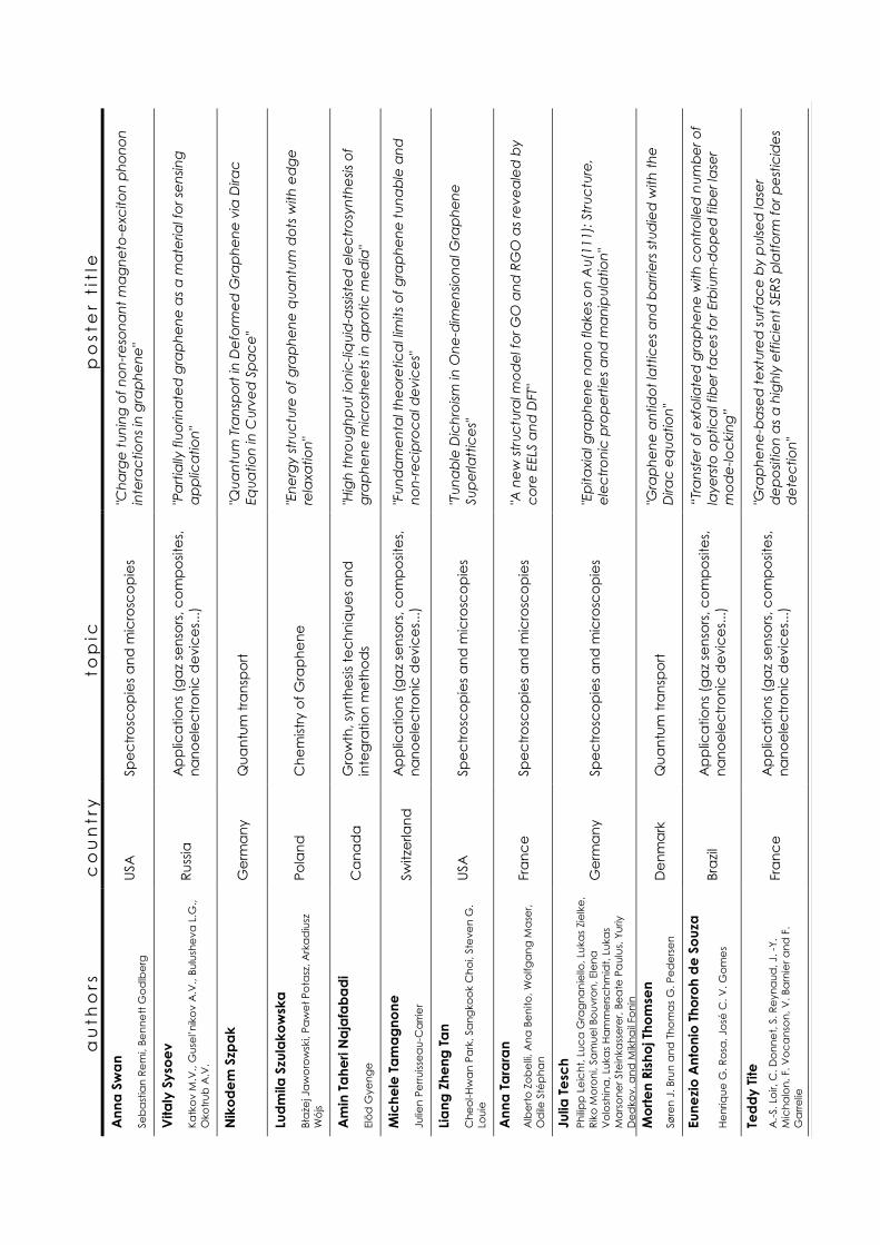
au
th
ors
c
ou
ntry
to
pic
p
os
te
r t
itle
An
na
Sw
an
U
SA
Sp
ec
tro
sco
pie
s a
nd
mic
rosc
op
ies
"Ch
arg
e t
un
ing
of
no
n-r
eso
na
nt
ma
gn
eto
-exc
ito
n p
ho
no
n
inte
rac
tio
ns
in g
rap
he
ne
" Se
ba
stia
n R
em
i, B
en
ne
tt G
od
lbe
rg
Vita
ly S
yso
ev
Ru
ssia
A
pp
lica
tio
ns
(ga
z se
nso
rs, c
om
po
site
s,
na
no
ele
ctr
on
ic d
evic
es.
..)
"Pa
rtia
lly f
luo
rin
ate
d g
rap
he
ne
as
a m
ate
ria
l fo
r se
nsi
ng
ap
plic
ati
on
" K
atk
ov M
.V., G
use
l’n
iko
v A
.V., B
ulu
she
va
L.G
.,
Oko
tru
b A
.V.
Nik
od
em
Szp
ak
G
erm
an
y
Qu
an
tum
tra
nsp
ort
"Q
ua
ntu
m T
ran
spo
rt in
De
form
ed
Gra
ph
en
e v
ia D
ira
c
Eq
ua
tio
n in
Cu
rve
d S
pa
ce
" Lu
dm
ila
Szu
lak
ow
ska
Po
lan
d
Ch
em
istr
y o
f G
rap
he
ne
"E
ne
rgy s
tru
ctu
re o
f g
rap
he
ne
qu
an
tum
do
ts w
ith
ed
ge
rela
xa
tio
n"
Bła
żej Ja
wo
row
ski,
Pa
we
ł P
ota
sz,
Ark
ad
iusz
Wó
js
Am
in T
ah
eri N
aja
fab
ad
i C
an
ad
a
Gro
wth
, sy
nth
esi
s te
ch
niq
ue
s a
nd
inte
gra
tio
n m
eth
od
s
"Hig
h t
hro
ug
hp
ut
ion
ic-liq
uid
-ass
iste
d e
lec
tro
syn
the
sis
of
gra
ph
en
e m
icro
she
ets
in a
pro
tic
me
dia
" Elö
d G
ye
ng
e
Mic
he
le T
am
ag
no
ne
Sw
itze
rla
nd
A
pp
lica
tio
ns
(ga
z se
nso
rs, c
om
po
site
s,
na
no
ele
ctr
on
ic d
evic
es.
..)
"Fu
nd
am
en
tal t
he
ore
tic
al l
imit
s o
f g
rap
he
ne
tu
na
ble
an
d
no
n-r
ec
ipro
ca
l d
ev
ice
s"
Ju
lien
Pe
rru
isse
au
-Ca
rrie
r
Lia
ng
Zh
en
g T
an
USA
Sp
ec
tro
sco
pie
s a
nd
mic
rosc
op
ies
"Tu
na
ble
Dic
hro
ism
in O
ne
-dim
en
sio
na
l G
rap
he
ne
Su
pe
rla
ttic
es"
C
he
ol-H
wa
n P
ark
, Sa
ng
ko
ok C
ho
i, S
teve
n G
.
Lou
ie
An
na
Ta
rara
n
Fra
nc
e
Sp
ec
tro
sco
pie
s a
nd
mic
rosc
op
ies
"A n
ew
str
uc
tura
l m
od
el f
or
GO
an
d R
GO
as
rev
ea
led
by
co
re E
ELS
an
d D
FT"
Alb
ert
o Z
ob
elli
, A
na
Be
nito
, W
olfg
an
g M
ase
r,
Od
ile S
tép
ha
n
Ju
lia
Te
sch
Ge
rma
ny
Sp
ec
tro
sco
pie
s a
nd
mic
rosc
op
ies
"Ep
ita
xia
l g
rap
he
ne
na
no
fla
ke
s o
n A
u(1
11
): S
tru
ctu
re,
ele
ctr
on
ic p
rop
ert
ies
an
d m
an
ipu
latio
n"
Ph
ilip
p L
eic
ht,
Lu
ca
Gra
gn
an
iello
, Lu
ka
s Zie
lke
,
Rik
o M
oro
ni,
Sa
mu
el B
ou
vro
n, Ele
na
Vo
losh
ina
, Lu
ka
s H
am
me
rsc
hm
idt,
Lu
ka
s
Ma
rso
ne
r Ste
inka
sse
rer,
Be
ate
Pa
ulu
s, Y
uriy
De
dko
v, a
nd
Mik
ha
il Fo
nin
Mo
rte
n R
ish
oj Th
om
sen
D
en
ma
rk
Qu
an
tum
tra
nsp
ort
"G
rap
he
ne
an
tid
ot
latt
ice
s a
nd
ba
rrie
rs s
tud
ied
with
th
e
Dira
c e
qu
ati
on
" Sø
ren
J. B
run
an
d T
ho
ma
s G
. P
ed
ers
en
Eu
ne
zio
An
ton
io T
ho
roh
de
So
uza
Bra
zil
Ap
plic
atio
ns
(ga
z se
nso
rs, c
om
po
site
s,
na
no
ele
ctr
on
ic d
evic
es.
..)
“Tr
an
sfe
r o
f e
xfo
liate
d g
rap
he
ne
with
co
ntr
olle
d n
um
be
r o
f
laye
rsto
op
tic
al f
ibe
r fa
ce
s fo
r Erb
ium
-do
pe
d f
ibe
r la
ser
mo
de
-lo
ckin
g”
He
nriq
ue
G. R
osa
, Jo
sé C
. V
. G
om
es
Ted
dy
Tite
Fra
nc
e
Ap
plic
atio
ns
(ga
z se
nso
rs, c
om
po
site
s,
na
no
ele
ctr
on
ic d
evic
es.
..)
"Gra
ph
en
e-b
ase
d t
ext
ure
d s
urf
ac
e b
y p
uls
ed
lase
r
de
po
siti
on
as
a h
igh
ly e
ffic
ien
t SER
S p
latf
orm
fo
r p
est
icid
es
de
tec
tio
n"
A.-
S. Lo
ir, C
. D
on
ne
t, S
. R
eyn
au
d, J.
-Y.
Mic
ha
lon
, F. V
oc
an
son
, V
. B
arn
ier
an
d F
.
Ga
rre
lie
au
th
ors
c
ou
ntry
to
pic
p
os
te
r t
itle
Yo
sra
To
um
ia
Ita
ly
Ap
plic
atio
ns
(ga
z se
nso
rs, c
om
po
site
s,
na
no
ele
ctr
on
ic d
evic
es.
..)
"Stu
dy o
n N
on
-co
va
len
tly S
tab
ilze
d G
rap
he
ne
in c
he
mic
al
PV
A-M
A b
ase
d H
yd
rog
el"
Silv
ia O
rla
nd
uc
ci a
nd
Ga
io P
ara
do
ssi
Ma
rio
Ita
lo T
rio
ni
Ita
ly
Qu
an
tum
tra
nsp
ort
"Ab
-in
itio
stu
dy o
f th
e e
lec
tric
fie
ld e
ffe
cts
pro
du
ce
d b
y
nitro
ge
n a
nd
bo
ron
do
pa
nts
on
th
e t
ran
spo
rt a
nd
ele
ctr
on
ic p
rop
ert
ies
of
the
bila
ye
r g
rap
he
ne
" D
an
iele
Gio
fré
, D
avid
e C
ere
soli
Da
mie
n T
rist
an
t
Fra
nc
e
Ch
em
istr
y o
f G
rap
he
ne
“Im
pro
ve
d t
he
co
nd
uc
tiv
ity o
f th
e c
arb
on
na
no
tub
es
by
iod
ine
do
pin
g: a
DFT
stu
dy”
Ian
n G
erb
er,
Pa
sca
l P
ue
ch
Via
ch
esl
av
Tu
r
Ru
ssia
G
row
th, sy
nth
esi
s te
ch
niq
ue
s a
nd
inte
gra
tio
n m
eth
od
s
"Pe
rfo
rati
on
of
the
Gra
ph
en
e L
aye
rs v
ia H
igh
Te
mp
era
ture
Ac
idic
Tre
atm
en
t o
f G
rap
hite
Oxid
e"
Fe
do
rovsk
aya
E.O
., B
ulu
she
va
L.G
., O
ko
tru
b
A.V
.
Tom
oh
isa
Uc
hid
a
Ja
pa
n
Qu
an
tum
tra
nsp
ort
"T
he
ory
of
qu
an
tum
Ha
ll e
ffe
ct
in g
rap
he
ne
" M
ah
o F
ujit
a,
Tad
ash
i To
yo
da
Ja
wa
d U
l H
ass
an
Sw
ed
en
G
row
th, sy
nth
esi
s te
ch
niq
ue
s a
nd
inte
gra
tio
n m
eth
od
s
"Qu
asi
-fre
e-s
tan
din
g m
on
ola
ye
r a
nd
bila
ye
r g
rap
he
ne
gro
wth
on
ho
mo
ep
ita
xia
l o
n-a
xis
4H
-SiC
(00
01
) la
ye
rs"
I. G
. Iv
an
ov, M
. W
inte
rs,
O. H
ab
ibp
ou
r, N
.
Ro
rsm
an
, a
nd
E. Ja
nzé
n
Crist
ian
Va
ca
ce
la
Ita
ly
Gro
wth
, sy
nth
esi
s te
ch
niq
ue
s a
nd
inte
gra
tio
n m
eth
od
s
"Hyd
roth
erm
al e
xfo
liati
on
of
gra
ph
ite
to
pro
du
ce
fe
w-la
ye
r
gra
ph
en
e"
Ga
brie
la T
ub
ón
, D
ian
a C
oe
llo, Lo
ren
zo
Ca
pu
ti,
Ad
alg
isa
Ta
vo
laro
Ja
rkk
o V
äh
äk
an
ga
s Fin
lan
d
Sp
ec
tro
sco
pie
s a
nd
mic
rosc
op
ies
"Ma
gn
eto
-Op
tic
Sp
ec
tro
sco
py o
f G
rap
he
ne
Qu
an
tum
Do
ts
by F
irst
Prin
cip
les"
P
ert
tu L
an
tto
an
d J
uh
a V
aa
ra
Fre
ia V
an
He
e
Be
lgiu
m
Sc
ien
tific
Po
licy
“FLA
G-E
RA
: (t
he
FLA
GSH
IP E
RA
-NET)
Co
ord
ina
tin
g N
ati
on
al
an
d R
eg
ion
al Fu
nd
ing
fo
r th
e F
ET
Fla
gsh
ips”
Ed
ou
ard
Ge
off
rois
Ma
tth
ias
Va
up
el
Ge
rma
ny
Sp
ec
tro
sco
pie
s a
nd
mic
rosc
op
ies
"To
po
gra
ph
y a
nd
ele
ctr
o-o
ptic
pro
pe
rtie
s o
f g
rap
he
ne
laye
rs m
ea
sure
d b
y c
orr
ela
tio
n o
f o
ptic
al in
terf
ere
nc
e
co
ntr
ast
, a
tom
ic f
orc
e,
an
d b
ac
k s
ca
tte
red
ele
ctr
on
mic
rosc
op
y"
An
ke
Du
tsc
hke
, U
lric
h W
urs
tba
ue
r ,
Fra
nk
Hitze
l
Do
min
iqu
e V
ign
au
d
Fra
nc
e
Gro
wth
, sy
nth
esi
s te
ch
niq
ue
s a
nd
inte
gra
tio
n m
eth
od
s
"Sc
an
nin
g t
un
ne
ling
mic
rosc
op
y a
nd
an
gle
-re
solv
ed
ph
oto
ele
ctr
on
sp
ec
tro
sco
py s
tud
ies
of
gra
ph
en
e o
n S
iC (
C-
fac
e)
sub
stra
te g
row
n b
y S
i flu
x-a
ssis
ted
mo
lec
ula
r b
ea
m
ep
ita
xy"
I. R
aza
do
-Co
lam
bo
, J.-
P.
Nys,
X.
Wa
llart
, S.
Go
de
y, J.
Av
ila, M
.-C
. A
sen
sio
Se
rgio
Vla
ic
Fra
nc
e
Sp
ec
tro
sco
pie
s a
nd
mic
rosc
op
ies
"Ele
me
nta
ry p
roc
ess
es
an
d f
ac
tors
influ
en
cin
g t
he
inte
rca
lati
on
be
twe
en
gra
ph
en
e a
nd
irid
ium
" A
min
a K
imo
uc
he
, Jo
ha
nn
Co
rau
x,
Be
nito
Sa
nto
s, A
nd
rea
Lo
ca
telli
, N
ico
las
Ro
ug
em
aill
e
au
th
ors
c
ou
ntry
to
pic
p
os
te
r t
itle
Xin
ran
Wa
ng
Ch
ina
A
pp
lica
tio
ns
(ga
z se
nso
rs, c
om
po
site
s,
na
no
ele
ctr
on
ic d
evic
es.
..)
"Tu
na
ble
, U
ltra
low
-Po
we
r Sw
itc
hin
g in
Me
mrist
ive
De
vic
es
En
ab
led
by G
rap
he
ne
-Oxid
e H
ete
rog
en
eo
us
Inte
rfa
ce
" M
in Q
ian
, Y
imin
g P
an
, Fe
ng
yu
an
Liu
, M
iao
Wa
ng
, H
ao
lian
g S
he
n,
Da
ow
ei H
e,
Ba
ige
ng
Wa
ng
, Y
i Sh
i an
d F
en
g M
iao
Yu
Wa
ng
Fra
nc
e
Ch
em
istr
y o
f G
rap
he
ne
"G
rap
he
nid
e S
olu
tio
ns
an
d F
ilms"
K
ai H
ua
ng
, A
lain
De
rré
, C
élia
Ca
stro
, La
ure
No
é, P
asc
al P
ue
ch
, M
arc
Mo
nth
iou
x, Sté
ph
an
Ro
uzi
ère
,Pa
sca
le L
au
no
is, Ia
nn
Ge
rbe
r, A
lain
Pé
nic
au
d
Hir
osh
i W
ata
na
be
Ja
pa
n
Sp
ec
tro
sco
pie
s a
nd
mic
rosc
op
ies
"Fe
mto
sec
on
d m
id-in
fra
red
lum
ine
sce
nc
e w
ith
ho
t-p
ho
no
n
eff
ec
ts in
gra
ph
en
es
an
d g
rap
hite
" To
mo
hiro
Ka
wa
saki, a
nd
To
hru
Su
em
oto
Ste
ffe
n W
eik
ert
Ge
rma
ny
Gro
wth
, sy
nth
esi
s te
ch
niq
ue
s a
nd
inte
gra
tio
n m
eth
od
s
"Do
pin
g o
f g
rap
he
ne
with
N+
an
d B
+ io
ns
by lo
w-e
ne
rgy io
n
irra
dia
tio
n"
Ju
lian
Ale
xa
nd
er
Am
an
i, P
hili
p W
illke
, H
an
s
Ho
fsä
ss, M
art
in W
en
de
roth
Ru
ne
We
nd
elb
o
No
rwa
y
Gro
wth
, sy
nth
esi
s te
ch
niq
ue
s a
nd
inte
gra
tio
n m
eth
od
s
"In
du
stria
l Sc
ale
Gra
ph
en
e O
xid
e P
rod
uc
tio
n a
nd
Ap
plic
ati
on
" Sa
me
er
Fo
ted
ar
an
d E
ina
r Eile
rtse
n
Ru
ne
We
nd
elb
o
No
rwa
y
Gro
wth
, sy
nth
esi
s te
ch
niq
ue
s a
nd
inte
gra
tio
n m
eth
od
s
"Re
du
ce
d G
rap
he
ne
oxid
e d
ec
ora
tio
n w
ith
fu
nc
tio
na
l
na
no
-cry
sta
ls"
Sa
me
er
Fo
ted
ar
an
d V
olo
dym
ir Y
art
is
Pa
tric
k W
he
lan
De
nm
ark
G
row
th, sy
nth
esi
s te
ch
niq
ue
s a
nd
inte
gra
tio
n m
eth
od
s
"Oxid
ati
ve
de
co
up
ling
tra
nsf
er:
th
e in
flu
en
ce
of
co
pp
er
oxid
ati
on
on
CV
D g
rap
he
ne
tra
nsf
er"
N
ata
lie V
. K
ost
esh
a, Fili
pp
o P
izzo
cc
he
ro, P
ete
r
Bø
gg
ild,
Tim
oth
y J
. B
oo
th
Leo
nie
Wib
me
r
Ge
rma
ny
Sp
ec
tro
sco
pie
s a
nd
mic
rosc
op
ies
"Ph
oto
ph
ysi
ca
l In
tera
ctio
ns
of
Ph
tha
loc
ya
nin
es
with
Gra
ph
en
e N
an
osh
ee
ts"
Lea
nd
ro M
. O
. Lo
ure
nç
o,
Ale
xa
nd
ra R
oth
,
Ge
org
ios
Ka
tsu
kis
, To
má
s To
rre
s, D
irk M
. G
uld
i
Qu
en
tin
Wilm
art
Fra
nc
e
Qu
an
tum
tra
nsp
ort
"K
lein
-tu
nn
elin
g t
ran
sist
or
with
ba
llist
ic g
rap
he
ne
" S. B
err
ad
a, V
. H
un
g N
gu
ye
n, G
. Fè
ve
, J.M
.
Be
rro
ir,
P. D
ollf
us,
B.
Pla
ça
is
Mic
ha
el W
inte
rs
Sw
ed
en
A
pp
lica
tio
ns
(ga
z se
nso
rs, c
om
po
site
s,
na
no
ele
ctr
on
ic d
evic
es.
..)
"Th
e C
V C
ha
rac
terist
ic o
f H
-in
terc
ala
ted
Ep
ita
xia
l
Gra
ph
en
e/A
l 2O
3 M
OS C
ap
ac
ito
rs"
Ein
ar
Örn
Sve
inb
jörn
sso
n,
Om
id H
ab
ibp
ou
r,
Ja
wa
d u
l-H
ass
an
, Erik J
an
zén
, N
ikla
s R
ors
ma
n,
He
rbe
rt Z
ira
th
Igo
r W
lasn
y
Po
lan
d
Ap
plic
atio
ns
(ga
z se
nso
rs, c
om
po
site
s,
na
no
ele
ctr
on
ic d
evic
es.
..)
"Gra
ph
en
e p
rin
tin
g f
or
fle
xib
le e
lec
tro
nic
s"
M. R
og
ala
, P
. J. K
ow
alc
zyk,
A.
Bu
sia
kie
wic
z, W
.
Ko
zlo
wsk
i, L
. Lip
insk
a, J. Ja
gie
llo, M
.
Aksi
en
ion
ek,
W.
Stu
pin
ski, P
. D
ab
row
ski,
Z.
Sie
rad
zki,
I. K
ruc
insk
a, M
. P
uc
ha
lski, E
.
Skrz
etu
ska
, Z.
Klu
sek
au
th
ors
c
ou
ntry
to
pic
p
os
te
r t
itle
Eu
nA
Wo
n
Ko
rea
A
pp
lica
tio
ns
(ga
z se
nso
rs, c
om
po
site
s,
na
no
ele
ctr
on
ic d
evic
es.
..)
"Stu
dy o
n O
ve
rla
pp
ing
Gra
ph
en
e a
nd
In
ZnO
Th
in F
ilm f
or
Ac
tiv
e la
ye
r o
f Tr
an
sist
or"
Jih
oo
n J
eo
n,
Ch
an
soo
Yo
on
, Sa
ng
ik L
ee
,
Miju
ng
Le
e, B
ae
ho
Pa
rk
Hu
aq
ian
g W
u
Ch
ina
A
pp
lica
tio
ns
(ga
z se
nso
rs, c
om
po
site
s,
na
no
ele
ctr
on
ic d
evic
es.
..)
"In
ve
rte
d P
roc
ess
Im
ple
me
nta
tio
n o
f M
on
olit
hic
Gra
ph
en
e
Mix
er"
H
on
gm
ing
Lv, H
e Q
ian
Hu
aq
ian
g W
u
Ch
ina
G
row
th, sy
nth
esi
s te
ch
niq
ue
s a
nd
inte
gra
tio
n m
eth
od
s
“R
ed
istr
ibu
tio
n o
f C
arb
on
Ato
ms
in P
t Su
bst
rate
fo
r H
igh
Qu
alit
y M
on
ola
ye
r G
rap
he
ne
Syn
the
sis”
Y
inyin
g L
i,X
iao
min
g W
u, H
e Q
ian
Yin
g W
u
UK
A
pp
lica
tio
ns
(ga
z se
nso
rs, c
om
po
site
s,
na
no
ele
ctr
on
ic d
evic
es.
..)
"A D
FTB
-ba
sed
ap
pro
ac
h t
o c
ha
rge
an
d d
ipo
le s
cre
en
ing
for
sp2
-bo
nd
ed
ca
rbo
n m
ate
ria
ls"
Ad
elin
a Ilie
, Sim
on
Cra
mp
in
Zh
on
g-S
hu
ai W
u
Ge
rma
ny
Ap
plic
atio
ns
(ga
z se
nso
rs, c
om
po
site
s,
na
no
ele
ctr
on
ic d
evic
es.
..)
"Gra
ph
en
e-B
ase
d M
icro
-Su
pe
rca
pa
cito
rs w
ith
Ultra
hig
h
Po
we
r a
nd
En
erg
y D
en
sitie
s"
Kh
ale
d P
arv
ez,
Xin
lian
g F
en
g, a
nd
Kla
us
Mü
llen
Xia
oq
ing
Ya
n
Ch
ina
Sp
ec
tro
sco
pie
s a
nd
mic
rosc
op
ies
"Po
lariza
tio
n-d
ep
en
de
nt
ultra
fast
op
tic
al r
esp
on
se in
gra
ph
en
e"
Zh
i-B
o L
iu, Ju
n Y
ao
, X
in Z
ha
o, X
u-D
on
g C
he
n,
Xia
ng
-Tia
n K
on
g, Fe
i X
ing
, Y
on
gsh
en
g C
he
n,
an
d J
ian
-Gu
o T
ian
Ho
ng
xin
Ya
ng
Fra
nc
e
Ma
gn
etism
an
d S
pin
tro
nic
s "A
na
tom
y o
f P
erp
en
dic
ula
r M
ag
ne
tic
An
iso
tro
py f
or
Co
ba
lt
film
s o
n G
rap
he
ne
" A
li H
alla
l, a
nd
Ma
irb
ek C
hsh
iev
Sh
ih C
hi Y
an
g
Taiw
an
O
the
r 2
dim
en
sio
na
l ma
teria
ls
"Se
lec
tive
De
po
sitio
n o
f H
igh
-k C
ap
pin
g L
aye
r o
n M
oS2
Fie
ld
Eff
ec
t Tr
an
sist
ors
by U
sin
g G
rap
he
ne
Ele
ctr
od
es"
C
he
-Hsu
an
Ch
en
g, C
hu
n-Y
ua
n H
sue
h, a
nd
Si-
Ch
en
Le
e
Vo
lod
ym
yr
Ya
rty
s
No
rwa
y
Ch
em
istr
y o
f G
rap
he
ne
"G
rap
he
ne
-ba
sed
ma
teria
ls f
or
en
erg
y s
tora
ge
: sy
nth
esi
s
an
d p
rop
ert
ies"
Y
.M. Sh
ulg
a, V
.A. Sm
irn
ov
, S.A
. B
ask
ako
v,
A.S
.
Arb
uzo
v,
B.P
. Ta
raso
v
Se
on
g J
un
Yo
on
K
ore
a
Ap
plic
atio
ns
(ga
z se
nso
rs, c
om
po
site
s,
na
no
ele
ctr
on
ic d
evic
es.
..)
"Eff
ec
t o
f R
ed
uc
ed
Gra
ph
en
e O
xid
e C
ap
La
ye
r o
n
Ele
ctr
om
igra
tio
n R
elia
bili
ty o
f C
u In
terc
on
ne
ct"
Su
ng
-Yo
ol C
ho
i, a
nd
Byu
ng
Jin
Ch
o
Jin
ka
i Y
ua
n
Fra
nc
e
Ap
plic
atio
ns
(ga
z se
nso
rs, c
om
po
site
s,
na
no
ele
ctr
on
ic d
evic
es.
..)
"Ele
ctr
ost
ric
tiv
e N
an
oc
om
po
site
s b
ase
d o
n R
ed
uc
ed
Gra
ph
en
e O
xid
e f
or
Me
ch
an
ica
l En
erg
y H
arv
est
ing
" W
ilfrid
Ne
ri,
Cé
cile
Za
kri,
An
nie
Co
lin, P
hili
pp
e
Po
ulin
Ze
ila
Za
no
lli
Ge
rma
ny
Ma
gn
etism
an
d S
pin
tro
nic
s "G
rap
he
ne
-mu
ltife
rro
ic h
ete
rost
ruc
ture
s: e
lec
tro
nic
an
d
ma
gn
eti
c p
rop
ert
ies
by d
esi
gn
" P
av
el Ze
len
ovsk
iy
Ru
ssia
Sp
ec
tro
sco
pie
s a
nd
mic
rosc
op
ies
"Str
ess
es
Ind
uc
ed
Pie
zoe
lec
tric
Re
spo
nse
in M
on
ola
ye
r
Gra
ph
en
e"
G.R
.Cu
nh
a, M
.K.S
ing
h,
A.L
.Kh
olk
in, V
.Ya
.Sh
ur
Jin
Zh
an
g
Ch
ina
Sp
ec
tro
sco
pie
s a
nd
mic
rosc
op
ies
"Gra
ph
en
e: A
Pla
tfo
rm f
or
Su
rfa
ce
En
ha
nc
ed
Ra
ma
n
Sp
ec
tro
sco
py"

au
th
ors
c
ou
ntry
to
pic
p
os
te
r t
itle
Ya
nfe
ng
Zh
an
g
Ch
ina
Sp
ec
tro
sco
pie
s a
nd
mic
rosc
op
ies
"Gro
wth
an
d a
tom
ic-s
ca
le c
ha
rac
teriza
tio
n o
f g
rap
he
ne
an
d g
rap
he
ne
-h-B
N h
yb
rid
on
me
tal su
bst
rate
s"
Me
ng
xi L
iu,
Ya
bo
Ga
o, Zh
on
gfa
n L
iu
Xia
o-M
ing
Zh
ao
C
hin
a
Ap
plic
atio
ns
(ga
z se
nso
rs, c
om
po
site
s,
na
no
ele
ctr
on
ic d
evic
es.
..)
"Ze
ro m
od
es
aro
un
d v
ac
an
cie
s in
to
po
log
ica
l in
sula
tors
an
d
top
olo
gic
al su
pe
rco
nd
uc
tors
on
th
e h
on
eyc
om
b la
ttic
e
wit
h p
art
icle
-ho
le s
ym
me
try"
Jin
g H
e, Su
-Pe
ng
Ko
u,
et
al.
Na
n Z
hu
De
nm
ark
A
pp
lica
tio
ns
(ga
z se
nso
rs, c
om
po
site
s,
na
no
ele
ctr
on
ic d
evic
es.
..)
"Gra
ph
en
e P
ap
er
Do
pe
d w
ith
Ch
em
ica
lly C
om
pa
tib
le
Pru
ssia
n B
lue
Na
no
pa
rtic
les
as
Na
no
hyb
rid
Ele
ctr
oc
ata
lyst
" Je
ns
Uls
tru
p, Q
ijin
Ch
i, K
asp
er
Nø
rga
ard
an
d
Bo
W. La
urs
en
Ale
xa
nd
er
Zö
pfl
Ge
rma
ny
Ap
plic
atio
ns
(ga
z se
nso
rs, c
om
po
site
s,
na
no
ele
ctr
on
ic d
evic
es.
..)
"Ga
s Se
nsi
tive
Ch
em
ire
sist
ors
Ba
sed
on
Ch
em
ica
lly R
ed
uc
ed
Gra
ph
en
e O
xid
e"
Tho
ma
s H
irsc
h, G
ün
the
r R
uh
l, F
ran
k-M
. M
aty
sik

Field Effect, Stain and Doping in Graphene Antidot Lattice
David M.A. Mackenzie, Lene Gammelgaard, Alberto Cagliani, Martin B.B.S Larsen, Bjarke S. Jessen, Mikkel Buster Klarskov and Peter Bøggild
DTU Nanotech, Technical University of Denmark, 2800 Kgs. Lyngby, Denmark
Graphene has been predicted to become widely integrated into future electronics, including high-speed transistor-based devices due to the reports of extreme mobilities [1]. While the lack of a bandgap prevents the necessary on/off ratios for such applications [2], several strategies have proven successful in inducing a transport gap. Among these, an antidot lattice allows not only introduction of a controllable bandgap, it also offers the intriguing possibility to guide electrons in a manner analogous to light in photonic bandgap structures [3]. Nanopatterning invariably introduces additional scattering and subsequent decreases in carrier mobility. It has, however, been predicted that just a fewer number of antidot rows can lead to a bandgap similar to that of a semi-infinite array, while maintaining an acceptable carrier mobility [4]. This study presents preliminary measurements on such devices. Single-layer graphene produced via the exfoliation method was patterned using electron-beam lithography and reactive ion etching, into multiple contact Hall bars, equipped with several antidot lattices. Each Hall-bar contained four sections: a pristine section as well as three patterned sections with either: one row of holes, five rows of holes or array of 48 rows of holes. This device enabled the simultaneous comparison of pristine graphene to graphene with a well-defined array of holes on the same graphene flake. The devices were fabricated on highly-doped silicon with a 300 nm silicon dioxide layer, which allowed back-gated measurements to be carried out. The electron and hole field-effect carrier mobilities as well as the gate bias required to observe a charge-neutrality point (CNP) were determined as a function of temperature (-195C to 150C). The temperature dependence of the antidots sections can be described as a combination of transport gap and variable range hoping, The prediction that a few rows of antidot leads to a minimal reduction of carrier mobility was confirmed. The interplay between nanopatterning, gate hysteresis and charge neutrality point offset was also studied. In order to determine if the fabrication of Hall bars using electron-beam lithography has any effect on the strain and doping levels, high-resolution micro-Raman maps were taking at several stages during the fabrication process. Using results from the literature [5] the changes in strain and doping can be tracked. Micro-Raman maps of several thousand points were taking directly after exfoliation, after cleaning, after deposition of metal contacts (defined using EBL), and finally after definition of Hall-bar structures. References [1] Geim & Novoselov, Nature Materials 6 (2007), 183 191. [2] Schwierz, Nature Nanotechnology, 5, (2010). 487 496 [3] Pedersen and Pedersen, Physical Review B 84 (2011), 115424 [4] Gunst et. al Physical Review, B 84, (2011) 155449 [5] Larsen et. al. MNE2013 Proceedings, In Press Figures
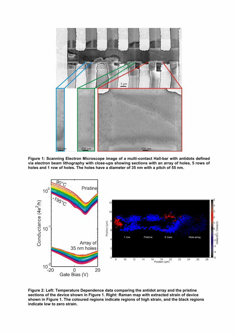
Figure 1: Scanning Electron Microscope image of a multi-contact Hall-bar with antidots defined via electron beam lithography with close-ups showing sections with an array of holes, 5 rows of holes and 1 row of holes. The holes have a diameter of 35 nm with a pitch of 55 nm.
Figure 2: Left: Temperature Dependence data comparing the antidot array and the pristine sections of the device shown in Figure 1. Right: Raman map with extracted strain of device shown in Figure 1. The coloured regions indicate regions of high strain, and the black regions indicate low to zero strain.

Magnetotransport properties of graphene devices contacted by resist-free stencil lithography
Ather Mahmood , Cheol-Soo Yang
§, Serin Park
§, Jean-François Dayen , Domink Metten , Stephane
Berciaud , Jeong-O Lee§ and Bernard Doudin *
Institut de Physique et Chimie des Matériaux de Strasbourg (IPCMS) and Laboratory NIE, University of Strasbourg, UMR 7504 CNRS-UdS, 23 rue du Loess, 67034 Strasbourg, France.
§Advanced Materials
Division, Korea Research Institute of Chemical Technology (KRICT) Daejeon, 305-343, South Korea
[email protected], [email protected]
Abstract We demonstrate large-scale fabrication of high-quality contaminant-free graphene devices,
which is a key prerequisite for chemical functionalization applications. We investigate CVD graphene
grown on Cu foil, subsequently transferred to Si/SiO2 substrates. Patterning of graphene and metal
evaporation for making contact wires and pads are performed through a multi-step mechanical stencils
methodology. Micro- and nanolithography through stencil masks is already well known, but graphene
device fabrication has seldom been achieved. In addition, the challenge remains to keep its outstanding
electrical properties intact. In order to prove the robustness of the devices fabricated with this non-
conventional lithography method, we have performed low-temperature magnetotransport measurements
on cross-bar shaped devices. Our results show the existence of Shubnikov-de Hass oscillations and
Quantum Hall (QH) Effect, the two hallmarks of good quality graphene. The corresponding Raman
spectroscopy maps show a low D peak and a 2D/G peak ratio of ~3, a further evidence for a defect-free
monolayer graphene device. Despite a certain degree of amorphization at the edges, the QH edge
states remain robust so as to allow the circulation of charge carriers.
To further characterize the disorder in graphene devices we study quantum transport properties,
sensitive to the nature of disorder in graphene. The presence of disorder (lattice defects, adsorbed
species, folds, ripples) entails Inter- and Intra-valley scattering processes as a result of symmetry
breaking at either A-B site or between adjacent valleys . Thus, depending on the intrinsic disorder,
presence of external potentials due to trapped charges in the oxide or at the interface, conventional
weak localization or weak (anti-) localization (WAL) can be observed in accordance with the recent WAL
theory on graphene. We use this theory to fit the experimental magnetoconductance data and extract
the values of scattering terms, validating the excellent intrinsic properties our samples. Finally, we show
that this technique can be extended to more complex geometries and smaller device feature sizes.
References [1] Y. X. Zhou, A. T. Johnson, J. Hone, W. F. Smith, Nano Lett. 2003, 3, 1371 1374. W. Bao, G. Liu, Z. Zhao, H. Zhang, D. Yan, A. Deshpande, B. LeRoy, C. N. Lau, Nano Res. 2010, 3, 98 102. [2] E. McCann, K. Kechedzhi, V. I. Falko, H. Suzuura, T. Ando, and B. L. Altshuler. Phys. Rev. Lett. 97, (2006) 146805. [3] V. I. Falko, K. Kechedzhi, E. McCann, and B. L. Altshuler H. Suzuura and T. Ando, Solid State Comm 143, (2007) 33. [4] X. Wu, X. Li, Z. Song, C. Berger, W.A. de Heer Phys. Rev. Lett. 98, 136801 (2007) [5] F. V. Tikhonenko, A. A. Kozikov, A. K. Savchenko, and R. V. Gorbachev, Phys. Rev. Lett. 103, (2009) 226801. [6] A. Mahmood, C. Naud, C. Bouvier, F. Hiebel, P. Mallet, J.-Y. Veuillen, L. P. Lévy, D. Chaussende, T. Ouisse, Journal of Applied Physics, 113, (2013) 083715.

Figure: (a) Stencil mask pattern used to define the graphene device shape. (b) Optical image of the cross-bar shaped graphene device with width 30 µm and length 250 µm. (c) 2D Raman map showing the I2D / IG peak ratio - the device shown in (c) with at various temperatures. Dotted lines are the experimental data whereas solid lines are fit according to theory.

Characterization of Few-layer Graphene (FLG) starting with Expanded Graphite
Sharali Malik
Institute of Nanotechnology, KIT, D-76131 Karlsruhe, Germany [email protected]
Abstract Graphene in currently moving swiftly from the research laboratory to the marketplace, driven by demand from markets where advanced materials are required. These include the aerospace, automotive, coatings, electronics, energy storage, coatings and paints, communications, sensor, solar, oil, and lubricant sectors. The exceptional electron and thermal transport, mechanical properties, barrier properties and high specific surface area of graphene and combinations thereof make it a potentially disruptive technology across a raft of industries. The European Union is funding a 10 year 1.35 billion euro coordination action on graphene. South Korea is spending $350 million on commercialization initiatives and the United Kingdom is investing £50million in a commercialization hub. Applications are coming onto the market for polymer composites and EMI shielding coatings. Graphene-based conducting inks are also finding their way into smart cards and radio-frequency identification tags. Many of the current and potential applications of carbon nanotubes may be taken by graphene as it displays enhanced properties but with greater ease of production and handling. Graphene, in common with graphite, is a pure carbon modification whose structure consists of two-dimensional sheets of aromatic carbon. The individual atoms are hexagonally arranged and form a wrinkled surface. The first synthesis of graphene was made in the late 19
th century [1], unfortunately
without any precise characterization. However, based on its promising properties, the general interest in this carbon material increased rapidly. After fullerenes in 1985 [2] and carbon nanotubes in 1991 [3],
unequivocally identified and studied by the physicists Andre Geim and Konstantin Novoselov [4]. In 2010, they both received the Nobel Prize in Physics for this work and are continuing to unveil new and exciting properties in graphene and other related two dimensional crystal materials. For specific applications, the term graphene can be divided into the sub-groups Single Layer Graphene (1 layer), Bi-Layer Graphene (2 layers) and Few-Layer Graphene (3 to 9 layers). As a result of the following versatile properties, graphene is a material of choice in the future:-
Chemical functionalization allowing improved compatibility in composite materials
High elasticity and tensile strength
Excellent barrier material for gas and liquids
High electrical and thermal conductivity
Microelectronics graphene transistors Possible future applications include:-
Electrically conductive inks for printable electronic circuits
LEC (Light-emitting electrochemical cell) ultra-thin energy efficient lighting for use in displays, cameras etc.
Stabilization of dispersions for better processability
Thin-film transistors vertical field-effect transistors
Impermeable membranes efficient release films, raingear, gas filters, electro-mechanical switches
The results of the new method to make few-layer graphene (FLG) look very promising so far as the FLG material has 1 to 6 layers. Fig. 1: SEM of FLG flakes and Fig. 2: Raman of one of the FLG flakes:-
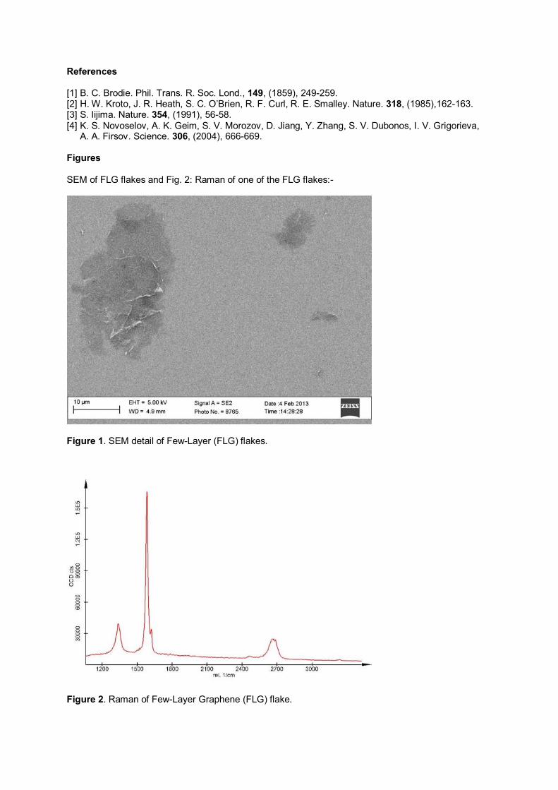
References [1] B. C. Brodie. Phil. Trans. R. Soc. Lond., 149, (1859), 249-259. [2] . Curl, R. E. Smalley. Nature. 318, (1985),162-163. [3] S. Iijima. Nature. 354, (1991), 56-58. [4] K. S. Novoselov, A. K. Geim, S. V. Morozov, D. Jiang, Y. Zhang, S. V. Dubonos, I. V. Grigorieva, A. A. Firsov. Science. 306, (2004), 666-669. Figures SEM of FLG flakes and Fig. 2: Raman of one of the FLG flakes:-
Figure 1. SEM detail of Few-Layer (FLG) flakes.
Figure 2. Raman of Few-Layer Graphene (FLG) flake.

Graphene Underlayer growth by chemical vapour deposition
Ncholu Manyala1, Mopeli Fabiane
1, Saleh Khamlich
1, Abdulhakeem Bello
1,
Julien Dangbegnon1, Damilola Momodu
1and A. T. Charlie Johnson
2
1Department of Physics, Institute of Applied Materials, SARChI Chair in Carbon Technology
and Materials, University of Pretoria, Pretoria 0028, South Africa2Department of Physics and Astronomy, University of Pennsylvania, Philadelphia,
Pennsylvania 19104, USA
Abstract Chemical vapor deposition (CVD) growth of graphene on copper foil has been regarded as more viable for obtaining monolayer graphene, mainly by a surface-controlled process [1. 2]. However, synthesizing uniform, defect-free multilayers has proved to be more difficult, and the growth mechanisms remain poorly understood. It has been observed that in the early stages of growth by CVD at atmospheric pressure, graphene on Cu foil forms as isolated “islands” which eventually coalesce to yield full, continuous monolayers. Occasionally these isolated islands are observed to have a second graphene layer which appears to nucleate at some sort of defect on the catalytic metal surface. It has often been assumed in the literature that the smaller islands are on top of the larger monolayer, and that they will grow and eventually form a second layer [3, 4–7]. However, Tontegode and co-workers [8, 9 had previously used Auger electron spectroscopy to suggest that graphene thick films grow in such a manner that the second and subsequent layers of graphene grow next to the substrate during segregation from Re-C solid solution and when carbon is deposited on Ir(111) in an inverted wedding cake fashion [10]. Recently, several groups have elucidated this underlayer growth mechanism of additional layers [11, 10, 12, 13]. However, the methods used in these studies were expensive and complex. For example, Nie et al.[11] proved that second-layer islands nucleate between the existing layer and the substrate. This they did by monitoring misalignment during growth on Ir(111) using a lowenergy electron diffraction (LEED) ultra-high vacuum chamber, angle-resolved photo-emission spectroscopy (ARPES) and low-energy electron microscopy (LEEM).Here we present a simple and very convincing approach to visualizing that subsequent layers of graphene grow between the existing monolayer graphene and the copper catalyst in chemical vapor deposition (CVD). Graphene samples were grown by CVD and then transferred onto glass substrates by the bubbling method in two ways, either direct-transfer (DT) to yield poly (methyl methacrylate) (PMMA)/graphene/glass or (2) inverted transfer (IT) to yield graphene/PMMA/glass. Field emission scanning electron microscopy (FE-SEM) and atomic force microscopy (AFM) were used to reveal surface features for both the DT and IT samples. The results from Raman spectroscopy, FE-SEM and AFM topographic analyses of the surfaces revealed the underlayer growth of subsequent layers. The subsequent layers in the IT samples are visualized as 3D structures, where the smaller graphene layers lie above the larger layers stacked in a concentric manner (see figures 1, 2 and 3 below). The results support the formation of the so-called “inverted wedding cake” stacking in multilayer graphene growth.
References
[1] C. Mattevi, H. Kima, and M. Chhowalla, J. Mater.Chem. 21, (2011) 3324.[2] E. G. Acheson, United States Patent 568323 (1896).[3] X. Li, W. Cai, L. Colombo, and R. S. Ruoff, Nano Lett. 9, (2009) 4268.[4] W. Wu, Q. Yu, P. Peng, Z. Liu, J. Bao, S. Pei, Nanotechnology 23, (2012) 035603.[5] C. Hwang, K. Yoo, S. J. Kim, E. K. Seo, H. Yu, and L. P. Bir, J. Phys. Chem. C 115, (2011) 22369.[6] I. Vlassiouk, M. Regmi, P. Fulvio, S. Dai, P. Datskos, G. Eres, and S. Smirnov, ACS Nano 5,
(2011) 6069.[8] A. Y. Tontegode, Prog. Surf. Sci. 38, (1991) 201.[9] N. R. Gall, E. V. Rut’Kov, and A. Y. Tontegode, Int. J. Mod. Phys. B 11, (1997) 1865.[10] S. Nie, W. Wu, S. Xing, Q. Yu, J. Bao, S. Pei, K. F. McCarty, New J Phys. 14, (2012) 093028.[11] S. Nie, A. L.Walter, N. C. Bartelt, E. Starodub, A. Bostwick, E. Rotenberg, and K. F. McCarty, ACS
Nano 5, (2011) 2298.[12] Q. Li, H. Chou, J. Zhong, J. Liu, A. Dolocan, J. Zhang, Y. Zhou, R. S. Ruoff, S. Chen, and W. Cai,
Nano Lett. 13, (2013) 486.

[13] W. Fang, A. L. Hsu, R. Caudillo, Y. Song, A. G. Birdwell, E. Zakar, M. Kalbac, M. Dubey, T. Palacios, M. S. Dresselhaus, P. T. Araujo, and J. Kong, Nano Lett. 13, (2013) 1541.
Fig. 3. Raman spectroscopy of the CVD graphene on glass substrate at two different spots indicated in the inset. (Inset) Raman map of the G-mode intensity showing a monolayer (blue circle) and few-layer graphene (green circle). Scale bar is 4 m in the inset.
Fig.1. FE-SEM images of: (a) direct-transfer (DT) graphene; (b) DT graphene on glass substrate taken at 70 with respect to the sample plane; (c) inverse-transfer (IT) graphene; and (d) high magnification of one of the islands in (c).
Fig. 2. 3D AFM image of one of the islands of the IT graphene sample.

Ultrathin metal films for direct thermochemical vapor deposition on dielectric substrates of single and a few layer graphene
Miriam Marchena, Valerio Pruneri
ICFO - Institut de Ciències Fotòniques - Parc Mediterrani de la Tecnologia, Av. del Canal Olímpic s/n 08860 Castelldefels, (Barcelona), Spain ICREA - Institució Catalana de Recerca i Estudis Avançats, 08010 Barcelona, Spain
Abstract
The thermochemical vapor deposition of single-few layer graphene on Ni and Cu metal films (UTMF) on glass substrates was proposed. In this paper, we investigate the possibility to use thinner metal films than previous studies, so called Ultrathin Metal Films (UTMFs), as thin as 7nm, as catalyst. We show that one can obtain improved quality grapheme over a larger area than previously demonstrated. The technique allows direct growth of graphene without significant increase of light reflection and absorption, thus offering the possibility to avoid cumbersome transfer after standard growth on much thicker (25- ) metal foils.
After evaluating the effect of the different process parameters, Ni of 7 and 50 nm thickness was
found to be more effective metal catalysts for graphene growth than Cu, despite the fact that solubility in Ni is higher and for this reason the tendency of multilayer graphene formation is increased. Ni is less prone to dewetting effects, i.e. metal retraction due to substrate heating. Experimentally, the minimum temperature at which graphene starts depositing has been determined to be 700ºC, and two different mechanisms of growth have been observed depending on the temperature and time: a) growth of graphene on top of ultrathin Ni without dewetting, at 700ºC, by increasing the reaction time, and b) growth of graphene in the dewetted area of Ni by increasing the temperature to 900ºC. References [1] Warner, Jamie H., Schäffel, F., Bachmatiuk, A., Rümmeli, Mark H., Elsevier, Graphene:
Fundamentals and emergent applications, (2013) 173-198. [2] Kim, H., Song, I., Park, C., Son, M., Hong, M., Kim, Y., Kim, J., Shin, H., Baik, J., Choi, H.C., ACS
Nano, Copper-Vapor-Assisted Chemical Vapor Deposition for High-Quality and Metal-Free Single-Layer graphene on amorphous SiO2 substrate, (2013).
[3] Patera, L., Africh, C., Weatherup, R., Blume, R., Bhardwaj, S., Castellarin-Cudia, C., Knop-Gericke, A., Schloegl, R., Comelli, G., Hofmann, S., Cepek, C., ACS Nano, In Situ observations of the atomistic mechanisms of Ni catalyzed low temperature graphene growth, (2013).
[4] Ismach, A., Druzgalski, C., Penwell, S., Schwartzberg, A., Zheng, M., Javey, A., Bokor, J., Zhang, Y., Nanoletters, Direct chemical vapor deposition of graphene on dielectric surfaces, (2010) 1542-1548. Figures
Table 1. Summary of the process conditions and characterization results
Metal
Catalyst Sample
Thick
(nm)
T
(ºC)
P
(mbar)
t
(min) CH4/H2 I2D/IG ID/IG
FWHM 2D
(cm-1
)
Ni
5/7/50 1000 7 30 1.5 0.297/1.331/2.334 1.394/0.865/0.047 43.3/35.9/26.4
50 700 7 30 1.5 5.847 1.118 22.8
50 900 7 30 1.5 2.280 0.492 29.7
7/50 1000 7 15 1.5 0.350/1.789 0.904/0.911 40.5/36.4
7/50 1000 7 60 1.5 0.425/2.793 1.250/0.528 34.4/27.6

Figure 2. Raman microscope pictures after graphene CVD on Ni (50 nm thick) at: a) SStarting of Ni dewetting where graphene grows suspended. Inset: SEM of the dewetted Ni, b) conditions. For increasing temperature, larger areas are dewetted and graphene progressively deposits in those areas.
1200 1400 1600 1800 2000 2200 2400 2600 2800
0
1000
2000
3000
4000
5000
6000
7000
8000
Inte
nsi
ty (
a.u
)
Raman shift (cm-1)
S1'_Ni50nm_1000ºC
S3'_Ni50nm_900ºC_non-dewetted region
S3'_Ni50nm_900ºC_dewetted region with Ni
S3'_Ni50nm_900ºC_dewetted region
S2'_Ni50nm_700ºC
1200 1400 1600 1800 2000 2200 2400 2600 2800
0
500
1000
1500
2000
2500
Inte
nsi
ty (
a.u
)
Raman shift (cm-1)
S5'_Ni50nm_60min
S1'_Ni50nm_30min
S4'_Ni50nm_15min
1200 1400 1600 1800 2000 2200 2400 2600 2800
0
500
1000
1500
2000
2500
3000
Inte
nsi
ty (
a.u
)Raman shift (cm
-1)
S1'_Ni50nm
S1'_Ni7nm
S1'_Ni5nm
Figure 2. Raman analysis after graphene CVD on Ni UTMF: a) Dependence on deposition
temperature, b) Dependence on deposition time and c) Dependence on Ni thickness.
Figure 3. SEM characterization of CVD graphene on Ni
dewetted and with high roughness where graphene is
suspended between the dewetted UTMF of Ni 0nm at 900ºC. Larger area has been dewetted
where graphene grows.
a) b) c)
a) b)

Method towards defect and residue free application of CVD graphene onto a surface
I. Martin-Fernandez1, E.S. Kulkarni
1,2, C.T. Toh
1, O. Kahya
1, H. Andersen
1,2, F. Giustiniano
1,
R. Bentini1, C.T. Cherian
1, A.V. Stier
1, B. Oezyilmaz
1,2
1 Graphene Research Centre and Dept. of Physics, National University of Singapore (NUS), Singapore.
2 National Graduate School for Integrative Sciences & Engineering (NGS), National University of Singapore (NUS), Singapore.
Graphene growth via chemical vapor deposition (CVD) on a metal catalyst promises to be the preferred method for large scale synthesis of graphene and graphene based electronic applications [1]. However, substrate and processing conditions of the device are usually incompatible with current CVD graphene growth technology, requiring the transfer of graphene from the growth substrate to the device surface. These additional transfer steps will result in defects in the graphene structure and in residues on the graphene surface that will worsen the characteristics of the graphene device. Different procedures to transfer graphene such as wet transfer, electrochemical delamination or tape-like methods [2] have been reported to yield large area transfer with minor quantity of defects and residues on the transferred graphene. However, these approaches have still not yielded totally clean and defect free graphene. Therefore, the transfer process continues to represent one of the main bottlenecks hindering the production of industrial scale graphene-based electronic applications. Here, we present a process for the transfer of CVD graphene with a minimal amount of residues. On the one hand, the metal catalyst residues on the graphene are reduced compared to the standard transfer process based on chemical etching of the metal catalyst. On the other hand, fewer residues from the transfer support are found compared to the polymer or tape based transfer methods. Thus, our process yields a cleaner graphene-target surface interface when compared to traditional polymer based counterparts. Our approach is industrially scalable and could, therefore, enable large area graphene based electronic applications. References [1] J. Ryu, et al., ACS Nano 8 (2014), 950-956. [2] J. Kang,et al., Nanoscale 4 (2012), 5527-5537.

Figures
Figure 1: Optical image (magnification is 100) of graphene transferred to a Si/SiO2 substrate. Cracks on the graphene are not appreciable at this magnification.
Figure 2: Maps of the D/G (a1, b1) and 2D/G (a2, b2) Raman peak ratios for graphene transferred by the wet transfer method (a1, a2) and graphene transferred by our method (b1, b2). The
average 2D/G and D/G peak ratios being alike evidences that our transfer method results in graphene that is as high quality as its wet transferred equivalent.

Epitaxial Graphene Growth and Shape Dynamics on Copper
Cecilia Mattevi
a, Esteban Meca
b, John Lowengrub
b, Hokwon Kim
c, Vivek B.
Shenoyd
aCASC, Department of Materials, Imperial College London, London SW7 2AZ, United Kingdom
bDepartment of Mathematics, University of California, Irvine, California 92697-3875, United States
a,cCEA, LETI, Minatec Campus, F-38054 Grenoble, France
d Department of Materials Science and Engineering, University of Pennsylvania, Philadelphia,
Pennsylvania 19104-6272, United States [email protected]
Abstract Synthesis of graphene on catalytic surfaces leads to formation of nuclei that can exhibit a variety of shapes from dendrites, squares, stars, hexagons, to butterflies and lobes. These shapes can further change over the growth time. Understanding the underlying mechanism which dictates the shape of the nuclei and their evolution over time has enabling potential for the engineering synthesis of wafer-scale single crystals. Here, we have studied the shape dynamics of graphene nuclei onto a variety of Cu facets [high symmetry facets such as (111) and (001) as well as for high-index surfaces such as (221) and (310)] under different growth parameters (CH4 flux, H2 flux and growth time) [1] with an objective to identify the role of different parameters. We have used a phase-field model to study the shape dynamics where we introduced anisotropies in the energies of growing graphene edges, in the kinetics of attachment of carbon at the edges and in the crystallinity of the underlying copper substrate (through anisotropy in surface diffusion). Our results show that anisotropic diffusion plays a critical role in determining the shape of islands, and the model can predict the growth shapes as a function of growth rate for different copper facets and synthesis conditions. References [1] Esteban Meca, John Lowengrub, Hokwon Kim, Cecilia Mattevi, and Vivek B. Shenoy Nano Lett., Nano Lett., 2013, 13 (11), pp 5692 5697
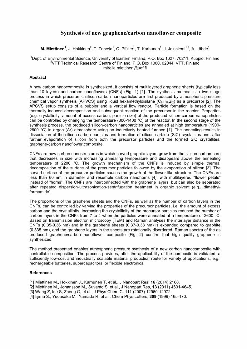
Synthesis of new graphene/carbon nanoflower composite
M. Miettinen1, J. Hokkinen
2, T. Torvela
1, C. Pfüller
1, T. Karhunen
1, J. Jokiniemi
1,2, A. Lähde
1
1Dept. of Environmental Science, University of Eastern Finland, P.O. Box 1627, 70211, Kuopio, Finland
2VTT Technical Research Centre of Finland, P.O. Box 1000, 02044, VTT, Finland
Abstract A new carbon nanocomposite is synthesized. It consists of multilayered graphene sheets (typically less than 10 layers) and carbon nanoflowers (CNFs) (Fig. 1) [1]. The synthesis method is a two stage process in which preceramic silicon-carbon nanoparticles are first produced by atmospheric pressure chemical vapor synthesis (APVCS) using liquid hexamethyldisilane (C6H18Si2) as a precursor [2]. The APCVS setup consists of a bubbler and a vertical flow reactor. Particle formation is based on the thermally induced decomposition and subsequent reaction of the precursor in the reactor. Properties (e.g. crystallinity, amount of excess carbon, particle size) of the produced silicon-carbon nanoparticles can be controlled by changing the temperature (800-1400 °C) of the reactor. In the second stage of the synthesis process, the produced silicon-carbon nanoparticles are annealed at high temperature (1900-2600 °C) in argon (Ar) atmosphere using an inductively heated furnace [1]. The annealing results in dissociation of the silicon-carbon particles and formation of silicon carbide (SiC) crystallites and, after further evaporation of silicon from both the precursor particles and the formed SiC crystallites, graphene-carbon nanoflower composite. CNFs are new carbon nanostructures in which curved graphite layers grow from the silicon-carbon core that decreases in size with increasing annealing temperature and disappears above the annealing temperature of 2200 °C. The growth mechanism of the CNFs is induced by simple thermal decomposition of the surface of the precursor particles followed by the evaporation of silicon [3]. The curved surface of the precursor particles causes the growth of the flower-like structure. The CNFs are less than 60 nm in diameter and resemble carbon nanohorns [4]
The CNFs are interconnected with the graphene layers, but can also be separated after repeated dispersion-ultrasonication-sentrifugation treatment in organic solvent (e.g., dimethyl-formamide). The proportions of the graphene sheets and the CNFs, as well as the number of carbon layers in the CNFs, can be controlled by varying the properties of the precursor particles, i.e. the amount of excess carbon and the crystallinity. Increasing the crystallinity of the precursor particles reduced the number of carbon layers in the CNFs from 7 to 4 when the particles were annealed at a temperature of 2600 °C. Based on transmission electron microscopy (TEM) and Raman analyses the interlayer distance in the CNFs (0.35-0.36 nm) and in the graphene sheets (0.37-0.38 nm) is expanded compared to graphite (0.335 nm), and the graphene layers in the sheets are rotationally disordered. Raman spectra of the as produced graphene/carbon nanoflower composite (Fig. 2) confirm that high quality graphene is synthesized. The method presented enables atmospheric pressure synthesis of a new carbon nanocomposite with controllable composition. The process provides, after the applicability of the composite is validated, a sufficiently low-cost and industrially scalable material production route for variety of applications, e.g., rechargeable batteries, supercapacitors, or flexible electronics. References [1] Miettinen M., Hokkinen J., Karhunen T. et al., J Nanopart Res, 16 (2014) 2168. [2] Miettinen M., Johansson M., Suvanto S. et al., J Nanopart Res, 13 (2011) 4631-4645. [3] Wang Z, Irle S, Zheng G, et al., J Phys Chem C, 111 (2007) 12960-12972. [4] Iijima S., Yudasaka M., Yamada R. et al., Chem Phys Letters, 309 (1999) 165-170.

Figures
1 µm
200 nm
2 nm
7 LAYERS
500 nm
A
B
Fig. 1 a) SEM and b) TEM images of synthesized graphene/carbon nanoflower composite. A higher magnification TEM image of the carbon nanoflowers is shown in subfigure b.
0
50
100
150
200
250
200 600 1000 1400 1800 2200 2600 3000 3400
Inte
nsi
ty (
arb
. u
nit
s)
Wavenumber (cm-1)
SPOT 1
SPOT 2
2D
-ba
nd
G-b
an
d
2D FWHM = 24 cm-1
2D FWHM = 46 cm-1
D-b
an
d
Fig. 2 Raman spectra of as produced graphene/carbon nanoflower composite.

Evaluation of the elastic constant C33 of multilayer graphene through the Layer Breathing Modes measured by Raman spectroscopy
S. Milana
1, D. Yoon
1, M. Ijäs
1, P. H. Tan
2, N. Pugno
3, A. C. Ferrari
1
1 Cambridge Graphene Centre, University of Cambridge, Cambridge CB3 0FA, United Kingdom
2 State Key Laboratory of Superlattices and Microstructures, Institute of Semiconductors, Chinese
Academy of Sciences, Beijing 100083, China 3 Department of Structural Engineering and Geotechnics, Politecnico di Torino, 10129 Torino, Italy
Contact: [email protected]
Abstract The set of elastic constants of a material is typically used to describe its mechanical properties. In crystals with uniaxial hexagonal layered structure such as graphite, the elasticity matrix describing mechanical properties contains five non vanishing, independent elastic moduli, namely C11, C12, C13, C33, and C44 [1]. In multilayer graphene, the elastic constants C11 and C12 are related to the strong bonding between carbon atoms within a layer, therefore describing in-plane deformations [2]. C44 represents the shear modulus of the layer-layer interface, accounting for displacement of the graphene planes with respect to each other [5]. C33 describing the out-of-plane compression or expansion of the graphene layers [2]. Raman spectroscopy is the prime nondestructive characterization tool for graphene and related layered materials [3, 4]. In layered crystals, the shear (C) [5] and layer breathing modes (LBMs) [3, 6, 7, 8], are due to relative motions of the planes, either perpendicular or parallel to their normal. According to these definitions, it is therefore possible to associate these Raman modes to their respective elastic constants accounting for such displacements. Here we measure by multi-wavelength Raman scattering the anti-Stokes and Stokes combinations of the G and LBM phonons in multilayer graphene, as a function of the number of layers (N), as shown in Fig. 1. By using a linear-chain model based on a normal interlayer force
constant per unit area, , we evaluate C33 of multilayer graphene to be 37 GPa. A similar Raman
analysis can be applied to any layered materials: the C33 of multilayer MoS2 is found to be 59.6 GPa. References [1] G. Grimvall, North-Holland (1986). [2] G. Savini, Y. J. Dappe, S. Oberg, J. C. M. I. Katsnelson, and A. Fasolino, Carbon, 49 (2011) 62. [3] A. C. Ferrari and D. M. Basko, Nat. Nanotechnol., 8 (2013) 235. [4] A. C. Ferrari, J. C. Meyer, V. Scardaci, C. Casiraghi, M. Lazzeri, F. Mauri, S. Piscanec, D. Jiang, K. S. Novoselov, S. Roth, A. K. Geim, Phys Rev Lett., 97 (2006) 187401. [5] P. H. Tan, W. P. Han, W. J. Zhao, Z. H. Wu, K. Chang, H. Wang, T. F. Wang, N. Bonini, N. Marzari, N. Pugno, G. Savini, A. Lombardo, and A. C. Ferrari, Nat. Mater., 11 (2012) 294. [6] X. Zhang, W. P. Han, J. B. Wu, S. Milana, Y. Lu, Q. Q. Li, A. C. Ferrari, P. H. Tan; Phys. Rev. B, 87 (2013) 115413. [7] F. Bonaccorso, P.H. Tan, A.C. Ferrari ; ACS Nano, 7(3) (2013) 1838. [8] F. Herziger, P. May, and J. Maultzsch, Phys. Rev. B, 85 (2012) 235447.
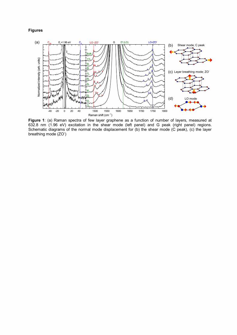
Figures
Figure 1: (a) Raman spectra of few layer graphene as a function of number of layers, measured at 632.8 nm (1.96 eV) excitation in the shear mode (left panel) and G peak (right panel) regions. Schematic diagrams of the normal mode displacement for (b) the shear mode (C peak), (c) the layer breathing mode (ZO )
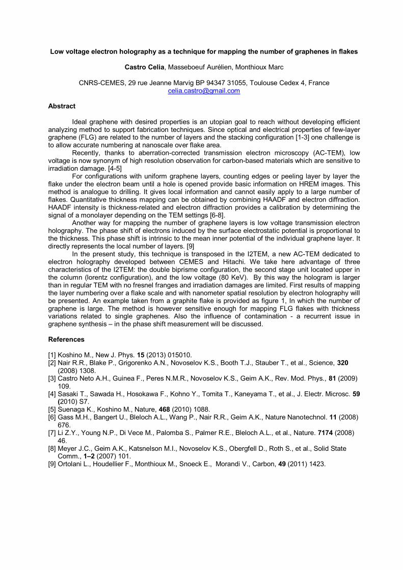
Low voltage electron holography as a technique for mapping the number of graphenes in flakes
Castro Celia, Masseboeuf Aurélien, Monthioux Marc
CNRS-CEMES, 29 rue Jeanne Marvig BP 94347 31055, Toulouse Cedex 4, France [email protected]
Abstract
Ideal graphene with desired properties is an utopian goal to reach without developing efficient analyzing method to support fabrication techniques. Since optical and electrical properties of few-layer graphene (FLG) are related to the number of layers and the stacking configuration [1-3] one challenge is to allow accurate numbering at nanoscale over flake area.
Recently, thanks to aberration-corrected transmission electron microscopy (AC-TEM), low voltage is now synonym of high resolution observation for carbon-based materials which are sensitive to irradiation damage. [4-5]
For configurations with uniform graphene layers, counting edges or peeling layer by layer the flake under the electron beam until a hole is opened provide basic information on HREM images. This method is analogue to drilling. It gives local information and cannot easily apply to a large number of flakes. Quantitative thickness mapping can be obtained by combining HAADF and electron diffraction. HAADF intensity is thickness-related and electron diffraction provides a calibration by determining the signal of a monolayer depending on the TEM settings [6-8].
Another way for mapping the number of graphene layers is low voltage transmission electron holography. The phase shift of electrons induced by the surface electrostatic potential is proportional to the thickness. This phase shift is intrinsic to the mean inner potential of the individual graphene layer. It directly represents the local number of layers. [9]
In the present study, this technique is transposed in the I2TEM, a new AC-TEM dedicated to electron holography developed between CEMES and Hitachi. We take here advantage of three characteristics of the I2TEM: the double biprisme configuration, the second stage unit located upper in the column (lorentz configuration), and the low voltage (80 KeV). By this way the hologram is larger than in regular TEM with no fresnel franges and irradiation damages are limited. First results of mapping the layer numbering over a flake scale and with nanometer spatial resolution by electron holography will be presented. An example taken from a graphite flake is provided as figure 1, In which the number of graphene is large. The method is however sensitive enough for mapping FLG flakes with thickness variations related to single graphenes. Also the influence of contamination - a recurrent issue in graphene synthesis in the phase shift measurement will be discussed. References
[1] Koshino M., New J. Phys. 15 (2013) 015010. [2] Nair R.R., Blake P., Grigorenko A.N., Novoselov K.S., Booth T.J., Stauber T., et al., Science, 320
(2008) 1308. [3] Castro Neto A.H., Guinea F., Peres N.M.R., Novoselov K.S., Geim A.K., Rev. Mod. Phys., 81 (2009)
109. [4] Sasaki T., Sawada H., Hosokawa F., Kohno Y., Tomita T., Kaneyama T., et al., J. Electr. Microsc. 59
(2010) S7. [5] Suenaga K., Koshino M., Nature, 468 (2010) 1088. [6] Gass M.H., Bangert U., Bleloch A.L., Wang P., Nair R.R., Geim A.K., Nature Nanotechnol. 11 (2008)
676. [7] Li Z.Y., Young N.P., Di Vece M., Palomba S., Palmer R.E., Bleloch A.L., et al., Nature. 7174 (2008)
46. [8] Meyer J.C., Geim A.K., Katsnelson M.I., Novoselov K.S., Obergfell D., Roth S., et al., Solid State
Comm., 1 2 (2007) 101. [9] Ortolani L., Houdellier F., Monthioux M., Snoeck E., Morandi V., Carbon, 49 (2011) 1423.

Figures
Figure 1: a) Electron hologram of a multi-graphene flake, b) Phase contour map every 10 graphene layers. Reported values represent local measurements.

The consequence of the turbostratic versus graphitic structure on the morphology of multi-graphene flakes
Laure Noé
a, Mathias Kobylko
a, Célia Castro
a, Thania Cazarès
a, Yu Wang
b, Marc Monthioux
a, Alain
Pénicaudb
a
tudes Structurales, UPR-8011 CNRS, University of Toulouse, BP 94347, F-31055 Toulouse, Cedex 4, France
b Centre de Recherche Paul Pascal, UPR-8641 CNRS, University of Bordeaux-I, 115, Avenue Albert
Schweitzer, 33600 Pessac, France [email protected]
Introduction Carbon objects made of several graphenes, here called multi-graphene flakes, may exhibit various morphologies. Whether the type of morphologies may somehow relate to the structural or nanotextural characteristics of the flakes was investigated by studying multi-graphene flakes originating from two kind of preparation routes. Synthesis and specimen preparation A solution of multi-graphene flakes was prepared by intercalation of natural graphite (with gaseous potassium) and then spontaneous exfoliation of the resulting KC8 graphite intercalation compound in an organic solvent (dimethylsulfoxid). The resulting graphene-based objects were studied by means of TEM and electron diffraction and compared to other graphene-based objects originating from a sublimation process. All objects exhibited dimensions in the range of several micrometers large, and with the number of stacked graphenes ranging from 2 to ~15. Results Two distinct morphologies were observed. The morphology of the flakes resulting from graphite exfoliation looks like a sheet of paper folded over itself, often several times, exhibiting straight fold edges and folding angles as multiples of 30° (Fig. 1, left). On the other hand, the morphology of the flakes originating from the sublimation process looks like a crumpled sheet of paper with no specific features but showing many folds and wrinkles (Fig. 1,right).
Figure 1. Example of multi-graphene flakes exhibiting the so-called 'folded' morphology (left) and the so-
called 'crumpled' morphology (right). Other multi-graphene flakes obtained from the exfoliation process showed an "intermediate" morphology, as they could hardly be put in one of both morphology categories above.
Interestingly, electron diffraction patterns related to each of the three morphology categories exhibited quite distinctive features. The folded morphology relates to flakes in which graphenes are stacked according the ABAB Bernal stacking sequence as in genuine graphite, as evidenced by the occurrence of hkl scattered beams such as 112 (Fig. 2, left). hk0 reflection spots are sharp, which relates to the relatively large lateral dimensions of the graphenes within coherent domains (i.e., crystals). Reflections involving 3D periodicities (such as 112) are sharp as well, which relates to the relatively high number of stacked graphenes in graphite crystals. hk0 reflections do not make continuous rings meaning that the number of coherent domains in the flake is few, but the different hk0 systems generated by different coherent domains (6 hk0 spots for each domain) frequently show relative orientation angles of nx30°. It is worth noting that the Bernal-stacked graphene flakes never exhibit the crumpled morphology, despite that mechanical constrains generated by surface tensions

developed during the drying process after the deposition of solution droplets onto the carbon film surface can be high.
On the contrary, the crumpled morphology relates to flakes in which graphenes within coherent domains are stacked according to the turbostratic structure (i.e., with full rotational disorder between each graphene in the stacking direction) as evidenced by the occurrence of the two Miller-indice scattered beams hk only (Fig.2, right). Because the graphenes have no orientational relationship, each graphene within every coherent domain contributes individually to the pattern by providing 6 hk spots each. The addition of all hk spots from all the graphenes builds continuous hk rings. Wrinkles and folds, which locally bring graphene planes under the Bragg angle, are so many and in all directions that the 00l spots generated by the stacking sequence in coherent domains are able to show up, also as a ring.
Figure 2. Example of electron diffraction pattern for a multi-graphene flake from the 'folded'
morphology(left) and from the 'crumpled' morphology (right). The folded versus crumpled morphological difference could be thought to originate from differences in flexural modulus induced by a dramatic difference in the number of graphenes involved in the coherent domains (the lower the number of graphenes, the lower the modulus). This was checked by high resolution TEM, which showed that the number of graphenes is large for both morphotypes, and even larger for the crumpled-type flakes, which goes against this possibility. Also, yet the graphenes in crumpled-type flakes exhibit more distortions than in folded-type flakes, the nanotexture (i.e., graphene perfection) is quite good in both flake types. Finally, flakes from the 'intermediate' category exhibit mixed features. Electron diffraction patterns show sharp, continuous yet dotted hk(0) rings, and a more or less faint 002 ring. Correspondingly, coherent domains in flakes are many and graphenes in the coherent domains are large, with no orientation relation to each other nor preferred folding directions. On the other hand, 112 reflections are present as a faint ring (i.e., not as sharp as the hk(0) rings) which means that the Bernal stacking sequence (ABAB) is present but involving few graphenes only (e.g., in the range of 2-3). The concomitant presence of individual graphenes and of turbostratic stacking is likely. Conclusion It is proposed that the type of structure is responsible for the type of morphology observed for graphene flakes, as Bernal (ABAB) sequence generate flakes with the folded morphology exhibiting nx30° folding features, indicating preferred folding directions in relation with that of the lattice. This is consistent with previous observations and supported by modelling [1]; (ii) coherent domains involving graphenes stacked according to the turbostratic sequence generate flakes with the crumpled morphology, whatever the number of graphenes involved, because no preferred lattice direction exists; (iii) coherent domains involving few (2-3) graphenes only, yet stacked according to the Bernal sequence, have a lesser propensity to lattice-driven folding, as a probable consequence of the lower flexural modulus. It is however believed that this discrimination between various morphotypes may occur only when the flakes have been subjected to events able to provide the energy needed to generate folds and wrinkles. Acknowledgments: This work was carried out within the the GRAAL project funded by the BLANC program of French ANR. References [1] Zhang J., Xiao J., Meng X., Monroe C., Huang Y., Zuo J.-M., Phys. Rev. Lett., 104 (2010) 166805.
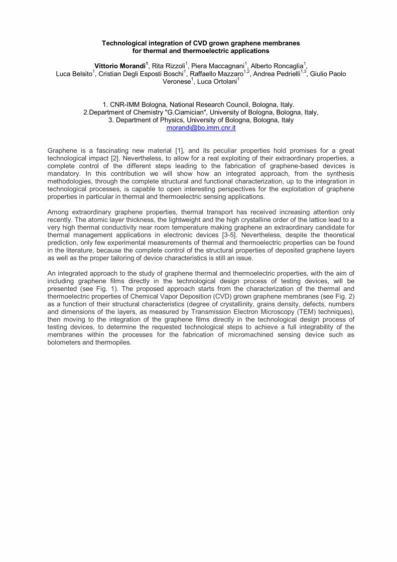
Technological integration of CVD grown graphene membranes
for thermal and thermoelectric applications
Vittorio Morandi1, Rita Rizzoli
1, Piera Maccagnani
1, Alberto Roncaglia
1,
Luca Belsito1, Cristian Degli Esposti Boschi
1, Raffaello Mazzaro
1,2, Andrea Pedrielli
1,3, Giulio Paolo
Veronese1, Luca Ortolani
1
1. CNR-IMM Bologna, National Research Council, Bologna, Italy. 2.Department of Chemistry "G.Ciamician", University of Bologna, Bologna, Italy,
3. Department of Physics, University of Bologna, Bologna, Italy [email protected]
Graphene is a fascinating new material [1], and its peculiar properties hold promises for a great technological impact [2]. Nevertheless, to allow for a real exploiting of their extraordinary properties, a complete control of the different steps leading to the fabrication of graphene-based devices is mandatory. In this contribution we will show how an integrated approach, from the synthesis methodologies, through the complete structural and functional characterization, up to the integration in technological processes, is capable to open interesting perspectives for the exploitation of graphene properties in particular in thermal and thermoelectric sensing applications. Among extraordinary graphene properties, thermal transport has received increasing attention only recently. The atomic layer thickness, the lightweight and the high crystalline order of the lattice lead to a very high thermal conductivity near room temperature making graphene an extraordinary candidate for thermal management applications in electronic devices [3-5]. Nevertheless, despite the theoretical prediction, only few experimental measurements of thermal and thermoelectric properties can be found in the literature, because the complete control of the structural properties of deposited graphene layers as well as the proper tailoring of device characteristics is still an issue. An integrated approach to the study of graphene thermal and thermoelectric properties, with the aim of including graphene films directly in the technological design process of testing devices, will be presented (see Fig. 1). The proposed approach starts from the characterization of the thermal and thermoelectric properties of Chemical Vapor Deposition (CVD) grown graphene membranes (see Fig. 2) as a function of their structural characteristics (degree of crystallinity, grains density, defects, numbers and dimensions of the layers, as measured by Transmission Electron Microscopy (TEM) techniques), then moving to the integration of the graphene films directly in the technological design process of testing devices, to determine the requested technological steps to achieve a full integrability of the membranes within the processes for the fabrication of micromachined sensing device such as bolometers and thermopiles.
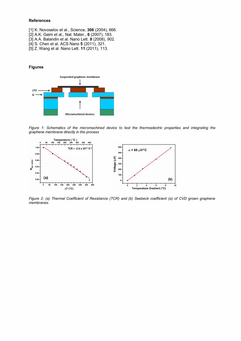
References [1] K. Novoselov et al., Science, 306 (2004), 666. [2] A.K. Geim et al., Nat. Mater., 6 (2007), 183. [3] A.A. Balandin et al. Nano Lett. 8 (2008), 902. [4] S. Chen et al. ACS Nano 5 (2011), 321. [5] Z. Wang et al. Nano Lett. 11 (2011), 113. Figures
Figure 1: Schematics of the micromachined device to test the thermoelectric properties and integrating the graphene membrane directly in the process
Figure 2: membranes.

Statistical Study on the Variation of Device Performance in CVD-grown Graphene FETs
C. Mukherjee, J. D. Aguirre-Morales, S. Fregonese, T. Zimmer and C. Maneux IMS Laboratory, UMR CNRS 5218, Cours de la Libération - 33405 Talence Cedex, Bordeaux, France
Abstract Following the recent discovery of graphene [1], its field-effect mobility as high as 15000 cm
2/V.s and a
Fermi velocity of ~108
cm/s have been demonstrated at room temperature [2]. These intriguing physical properties of graphene have accelerated rapid research activities for exploring its electronic properties further, most of which are yet to be unraveled. In this paper, we report a statistical study on the variation of performances observed from measurements of CVD-grown Graphene FETs (GFET) on different dies fabricated using identical process steps, reflecting on the process quality of Graphene layer as well as ohmic contact formations. The GFETs under study were characterized in several different dies using both current-voltage and S-parameter measurements under identical biasing conditions for the GFET gate width of 12 m and oxide thickness of 3 nm. The typical gate length used is 300 nm. The typical ID-VDS and ID-VGS are shown in Figure 1 depicting both measurement and simulation [3] results. The scalable electrical compact model developed in [3] is used here, which shows fair agreement with the measurement results. In Figure 2 (a), S parameters of a typical device after de-embedding are shown as a function of the frequency. The small signal model used to extract the parameters from the S-parameter measurements is shown to fit the experimental results in Figure 2(a). The magnitude of the current gain (H21) from both simulation and measurements are shown in Figure 2 (b) for three different samples on the same die with identical dimensions, depicting three different cut-off frequencies. Figure 3 illustrates the statistics on variation of On-current (Figure 3 (a)), and Dirac voltage (Figure 3 (b)) in the same die (D6). Figure 3 (c) shows the Dirac voltage as a function of the applied drain-source bias. The peak cut off frequencies obtained after de-embedding of S-parameters are shown in Figure 4 (a) for different devices on different dies. The results show a wide range of variation even in the same die. Similar statistics on the variation of other small-signal parameters (gm, gds, Cgs, Cgd, Rgs, Rgd and Rds) are shown in Figure 4 (b)-(d) as extracted from the de-embedded S-parameters. Note that, the Cds
capacitance extraction, in most of the devices, showed a very small value of about 1 aF. The variations observed for different parameters among the wide range of devices measured in different dies of the CVD-GFET reflect on the fact that even with identical dimensions and biasing conditions, the process quality of the Graphene transfer may play a major role in determining device performance despite good interface quality (as also indicated by negligible gate current in the devices). Also, as extracted from our measurement results, the drain-source access resistances may vary widely due to poor contact formation with the graphene (high contact resistances), resulting in fluctuation of device parameters. Thus, we can infer some new directives towards the possible future of Graphene-electronics regarding good quality of contacts with the Graphene as well as quality of the Graphene channel for future high-performance GFETs.
References [1] K. S. Novoselov, A. K. Geim, S. V. Morozov, D. Jiang, Y. Zhang, S. V. Dubonos, I. V. Grigorieva and A. A. Firsov, Science, 306 (2004) pp. 666-669. [2] A. K. Geim and K. S. Novoselov, Nature Materials, 6 (2007) pp. 183. [3] S. Fregonese, M. Magallo, C. Maneux, H. Happy, and T. Zimmer, IEEE Trans. Nanotechnology, 12(2013), pp. 539-546.
Figures
0.0 0.5 1.0 1.5 2.00.00
0.02
0.04
0.06
0.08
0.10
0.12
0.14
-2 -1 0 1 2
0.00
0.02
0.04
0.06
0.08
0.10
0.12
0.14
Measurement
Compact Model
I D (
mA
)
VDS
(V)
VGS
= - 1 to1 V
in 0.5V step
VDS
= 0 to2 V
in 0.5V step
VGS
(V)
Figure 1: Typical ID-VDS and ID-VGS characteristics of the GFET under study.
106
107
108
109
10-5
10-4
10-3
10-2
10-1
100
Model
Measurement
S12
S21
S22M
ag
(S P
ara
mete
r)
Frequency (Hz)
S11
(a)
0,01 0,1 10,1
1
10
100
1000
Model
Measurement
mag
(H2
1)
Frequency (GHz)
C_6_10
D_6_10
D_6_4
(b)
Figure 2: (a) Typical GFET S-parameters after de-embedding, (b) Magnitude of H21 for three GFETs.
(a)(b)
D_6_1
D_6_2
D_6_3
D_6_4
D_6_5
D_6_6
D_6_7
D_6_8
D_6_9
D_6_10
-10
0
10
20
30
40
50
60
Working Device Not Working
VDS
= 50 mV
I ON(
A)
D_6_2 D_6_3 D_6_4 D_6_5 D_6_9 D_6_100.0
0.2
0.4
0.6
0.8
1.0
1.2
1.4
50 mV
10 mV
VD
irac (
V)
VDS
0.0 0.3 0.6 0.9 1.2 1.5 1.8 2.10.0
0.5
1.0
1.5
2.0
2.5
3.0
Vd
ira
c (
V)
VDS
(V)
D_6_3
D_6_4
D_6_5
D_6_9
D_6_10
(c)
Figure 3: Statistics on the variation of (a) On-current, (b) Dirac voltage for the CVD GFETs on the same die (D6) for identical dimensions and biasing conditions, and (c) Dirac voltage as a function of VDS.
C_2_4
C_5_8
C_5_10
C_6_2
C_6_10
D_5_4
D_5_7
D_6_2
D_6_3
D_6_4
D_6_5
D_6_9
D_6_10
0.01
0.1
1
10
Pe
ak
fT (
GH
z)
C_2_4
C_5_8
C_5_10
C_6_2
C_6_10
D_5_4
D_5_7
D_6_2
D_6_3
D_6_4
D_6_5
D_6_9
D_6_10 --
10-15
10-14
10-13
Cgs
Cgd
Cg
s, C
gd (
F)
C_2_4
C_5_8
C_5_10
C_6_2
C_6_10
D_5_4
D_5_7
D_6_2
D_6_3
D_6_4
D_6_5
D_6_9
D_6_10
103
104
105 R
gs
Rds
Rgd
Rg
s, R
gd, R
ds (
)
C_2_4
C_5_8
C_5_10
C_6_2
C_6_10
D_5_4
D_5_7
D_6_2
D_6_3
D_6_4
D_6_5
D_6_9
D_6_10 --
0.000
0.001
0.002
0.003
0.004
-0.25
-0.20
-0.15
-0.10
-0.05
0.00
gm
gds
gd
s (
S)
gm(m
S)
(a) (b)
(c) (d)
Figure 4: Statistics of the variation of (a) peak cut-off frequency, (b) transconductance (gm, gds), (c) gate-source and gate-drain capacitances and (d) gate-source, gate-drain and drain-source resistances as extracted from the de-embedded S-parameters of the CVD-GFETs.
Non-thermal Reversibility by Ultraviolet Irradiation of Electron Mobility in Oxidized Graphene
Yana Mulyana, Mutsunori Uenuma, Yasuaki Ishikawa, Yukiharu Uraoka
Nara Institute of Science and Technology (NAIST), 8916-5 Takayama, Ikoma, Nara, 630-0192 Japan
Introduction The Hummers method is widely used for oxidation of graphene, despite resulting in a surface with
structural defects that degrades its characteristics, compromising its usability in high-performance devices. An alternative approach for oxidizing graphene using reactive atomic oxygen produced from oxygen molecules decomposed by a 1500ºC tungsten filament in an ultrahigh vacuum (UHV) to form graphene oxide (GO) with thermal reversibility at 260ºC has recently been reported.
1 However,
performing annealing treatment in UHV makes this method costly. Here, we presented a simpler and more cost-effective way to oxidize graphene layer through UV
(ultraviolet)/O3 (ozone) treatment and reduce the resulting GO through UV irradiation. Both oxidation and reduction were performed at ambient temperature in atmospheric pressure. The existence of chemical bonds between oxygen and graphene was confirmed from the XPS (X-ray photoelectron spectroscopy) spectra and directly observed by STM (scanning tunneling microscopy) topography. Moreover, changes in electrical properties of a single layer graphene-based field-effect transistor (G-FET) were also investigated. In previous works, we examined the thermal reversibility in electrical properties of a two-layer G-FET after being oxidized through UV/O3 treatment.
2 A decrease in
conductivity and carrier mobility was observed after oxidation, but the electrical properties recovered after subsequent H2/Ar annealing, indicating that the oxidation with UV/O3 treatment was thermally reversible. However, in current study we focused on the feasibility of non-thermal reduction of GO by UV irradiation which is more cost-effective than annealing in UHV. Experimental and Results
A single layer graphene film grown on thin copper sheet (1 x 1 cm) through chemical vapor deposition method (CVD-graphene) was UV/O3 treated for 6 min. In this treatment, oxygen gasses were channeled into a chamber, where CVD-graphene was placed inside, at a flow rate of 0.5 L/min and then ozonized using an ozone generator while simultaneously two types of ultraviolet light with wavelengths of 184.9 and 253.7 nm were produced from a low pressure mercury lamp to continuously generate reactive oxygen radicals. The STM topography of the pristine CVD-graphene and after being oxidized through UV/O3 treatment for 6 min are shown in Fig. 1 and 2, respectively. The height difference in pristine CVD-graphene was 0.1 nm and that in GO was 1 nm, 10 times greater, indicating the presence of chemically doped oxygen atoms on the graphene layer. The GO then was irradiated by UV light several times. Each UV irradiation was performed for 6 min using the same UV light used in UV/O3 treatment. XPS measurement was conducted to examine the concentration of doped oxygen which was
calculated from the XPS peak area ratio of C O (286.4 eV) and C C (284.8 eV). The change in
concentration of doped oxygen after each UV irradiation is shown in Fig. 3. The concentration of oxygen
increased after oxidation and then decreased after UV irradiation with no C O peak (288.9 eV)
observed, indicating that the GO was reduced without introducing lattice defects. The structure of single layer G-FET fabricated from exfoliated KISH graphite is shown in Fig. 4.
The transfer characteristics of the G-FET after first and second circle of oxidation and reduction processes are plotted in Fig. 5 and 6, respectively, where the ambipolar curve of graphene can be examined. The oxidation was performed through UV/O3 treatment for 3 min and reduction was performed through UV irradiation for 3 min. Electrical characterization of G-FET was carried out under a vacuum condition of 4.6 x 10
-5 Pa using a nano-probing microscopy (Hitachi NE4000). The slope of
ambipolar curve decreased after oxidation during the first redox process (Fig. 5), indicating the decreased electron mobility in graphene layer caused by the increased scattering due to the doped oxygen which obstructed the path of electron. However, a significant recovery of the ambipolar curve slope was observed after conducting UV irradiation, indicating that the GO was reduced and the electron mobility recovered. Since further recovery in the electron mobility was not observed after subsequent UV irradiation, then the second circle of redox process was undertaken. The change in behavior of ambipolar curve and electron mobility of G-FET after the second redox process (Fig. 6) was identical to the first redox process. The ambipolar curve significantly recovered to the state before oxidation after conducting UV irradiation three times. Therefore, after examining all these results, GO synthesized through UV/O3 treatment may be reduced non-thermally by UV irradiation, which is simpler and more cost-effective than annealing in UHV, without introducing significant lattice defects.

References
Figures
-
-
30
25
20
15
10
5
0
C-O concentration (%)
321 UV irradiation number
100
95
90
85
80
75
70
65
C-C concentration (%)
C-C
C-O
Pristine
Oxidationby UV/O3 treatment
Reductionby UV irradiation
Oxidationby UV/O3 treatment
7% of C=O detectedafter last oxidation
-
-
-
70
60
50
40
30
20
10
Dra
in C
urr
en
t (
A)
-40 -20 0 20 40
Back Gate Voltage (V)
After UV/O3 treatment
After 1st UV irradiation
After 2nd UV irradiation
Drain Voltage : 70 mV
70
60
50
40
30
20
10
Dra
in C
urr
en
t (
A)
-40 -20 0 20 40
Back Gate Voltage (V)
3 treatmentst UV irradiation
nd UV irradiation
rd UV irradiation
Drain Voltage : 70 mV
-

Terahertz radiation induced photocurrents in graphene with a lateral periodic potential
S. D. Ganichev1, J. Kamann
1, L. E. Golub
2, M. König
1, J. Eroms
1 ,M. Mittendorff
3, S. Winnerl
3, F.
Fromm4, Th. Seyller
4, and D. Weiss
1
1 University of Regensburg, Germany
2 Ioffe Physical-Technical Institute of the RAS, St. Petersburg, Russia
3 Helmholtz-Zentrum Dresden-Rossendorf, Germany
4 Technical University of Chemnitz, Germany
Abstract
We report on the observation of terahertz radiation induced photocurrents in graphene with a lateral periodic potential. These effects generate a dc electric current from an ac electric field. To enable the photocurrent generation a metal gratings have been deposited on top of graphene. The lateral potential is realized by electron beam lithography and subsequent deposition of a metal gate on top of the graphene layer. An insulating layer of aluminum oxide is used to separate gate and graphene. One set of samples (A) consists of periodically deposited stripes with different widths and spaces on epitaxial graphene grown on SiC (see Fig.1). Furthermore, we prepared exfoliated graphene flakes with an interdigitated double gate structure (B), where both gates can be controlled individually. Both types do not possess inversion symmetry.
We demonstrate that terahertz (THz) laser radiation (f = 2.54 THz, = 118 µm) shining on the modulated devices results in a directed electric current which is sensitive to the radiation polarization state. In particular a current which reverses its sign upon switching the photon helicity (i.e., it changes sign upon changing from left to right handed circular polarization) is detected (see Fig.2). To avoid illumination of the sample edges in samples (A), leading to edge photogalvanic currents [1], we use a large area of 4.5 × 4.5 mm
2 with a size larger than the laser spot. At normal incidence, the photocurrent
is only observed when the superlattice is illuminated, while no signal is observed on the unpatterned reference sample. This proves the symmetry breaking induced by the asymmetric lateral potential. Under oblique illumination the dynamic Hall effect leads to an additional current contribution [2]. The photocurrent cause by the lateral potential is shown to consist of two contributions; (i) polarization independent, and (ii) dependending on both the linear and circular polarization. The results are analysed in terms of the theory of ratchet effects in the structures with lateral potential [3,4] and of plasmonic Dyakonov-Shur mechanism in periodic structures [5]. The theory of the former one predicts that the photocurrent is controlled by elastic scattering processes and can be used to characterize the scattering mechanisms in graphene. In particular studying frequency dependence of the individual contributions to the photocurrent one can deduct the dominant elastic scattering mechanism in graphene. The frequency dependence was studied using the free-electron-laser FELBE at the HZDR. Our experimental findings can be well described by theory [4].
In addition to the large area structures (A), consisting of a single gate, we fabricated and studied photocurrent in interdigitated comb-like double-gate structures deposited on exfoliated graphene flakes. Each gate can be controlled separately; therefore, the intrinsic degree of the lateral potential asymmetry of the double-gate structures can be controllably varied. Investigation of the photocurrents in such type of structures provided an access to internal asymmetry of the graphene flakes. Moreover, we discuss the possibility to use such structures as a fast detector of terahertz radiation as it has been suggested in [5]. References [1] J. Karch et al., Phys. Rev. Lett. 107, 276601 (2011) [2] J. Karch et al., Phys. Rev. Lett. 105, 227402 (2010) [3] E. L. Ivchenko and S. D. Ganichev, JETP Lett. 93, 673 (2011). [4] A. V. Nalitov, L. E. Golub, and E. L. Ivchenko, Phys. Rev. B 86, 115301 (2012) [5] V. V. Popov, Apl. Phys. Lett. 102, 253504 (2013)
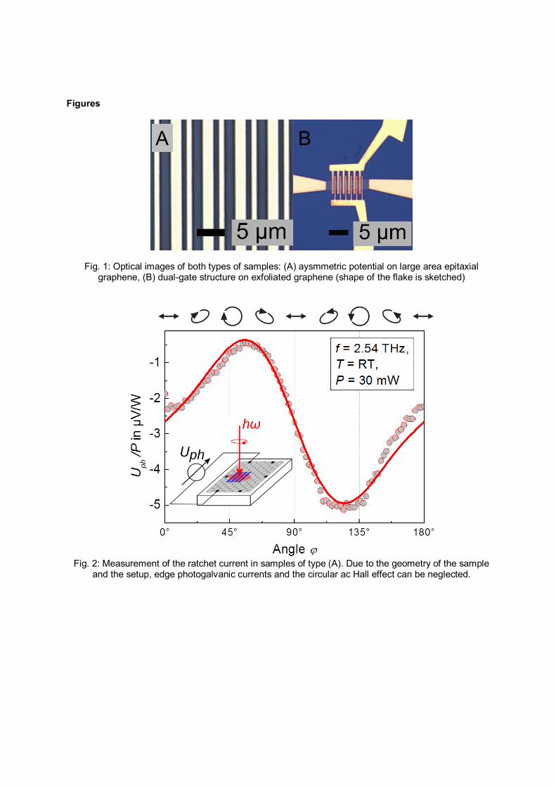
Figures
Fig. 1: Optical images of both types of samples: (A) aysmmetric potential on large area epitaxial graphene, (B) dual-gate structure on exfoliated graphene (shape of the flake is sketched)
Fig. 2: Measurement of the ratchet current in samples of type (A). Due to the geometry of the sample
and the setup, edge photogalvanic currents and the circular ac Hall effect can be neglected.
1
Non-Catalytic Growth of Nanographene Films on Silicon Oxide at Low Temperature
Roberto Muñoz*, Carmen Munuera, Mar García-Hernández, Cristina Gómez-Aleixandre
Materials Science Institute of Madrid, ICMM-CSIC,
Sor Juana Inés de La Cruz 3, 28049, Madrid, Spain
*E-mail: [email protected]
Abstract: Large area high quality, polycrystalline graphene and graphene single crystals can be grown
by chemical vapor deposition (CVD) on metals with promising results for many applications.[1,2]
At
present, this process is expensive owing to large energy consumption at the typical synthesis
temperature around 1000ºC and because underlying metal has to be removed. In this scenario, the
game changing breakthrough would be the development of processes to rapidly deposit high quality
graphene layers on arbitrary substrates, at low temperature.[3]
In this work we have faced this production challenge and we present the synthesis and systematic study
on nanographene based films directly grown on silicon oxide by using remote-ECR Plasma Assisted
CVD at low temperature (~550ºC).[4]
These films have been grown from different carbon sources (C2H2,
CH4) and carrier gases (H2, Ar). Optical Emission Spectroscopy (OES) allows us to inquire into the
differences in the composition of the generated plasmas and then to elucidate the main precursor
species that contribute to the film growth in each case. The fabrication process is rapid and performed
in large area (2 inch) dielectric substrates. TEM and electron diffraction analysis show the formation of
layered nanographene material. Raman Spectroscopy and AFM reveal that the film consists of
nanocrystals with a domain size between 2-10 nm depending on the synthesis conditions (figure 1),
usually interconnected by amorphous material. Functional optoelectric characterization of these films
confirms the high transparency over 95% and relative high
(figure 2), exceeding the properties of non-doped nanographene films grown at low temperatures
reported by far.[5]
This method avoids damaging and expensive transfer processes of nanographene
films and improves compatibility with current fabrication technologies. Moreover, tailored graphene
based structures and graphene flakes with nanometer-size can be synthesized by this method that open
the way for graphene chemistry and functionalization with straight application in several fields.[6]
Even
carbon and graphene nanodots under 10 nm size have recently attracted wide attention because of
their strong photoluminescence.[7]
These tiny dots could be attractive candidates for bioimaging and
biosensors.
References
[1] T. Kobayashi et al., Appl. Phys. Lett., 102 (2013) 023112. [2] Y. Hao, et al. Science, 342 (2013), 720.
[3] K.S. Novoselov, V.I. Falko, L. Colomo, P. R. Gellert, M. G. Schwab, K. Kim, Nature, 490, (2012),192.
[4] R. Muñoz and C. Gómez-Aleixandre, J. Phys. D: Appl. Phys, 47 (2014) 045305.
[5] H. Medina et al. Adv. Func. Mater, 22 (2012) 2123.
[6] H. Li et al., J. Mater. Chem., 22 (2012) 24230
[7] L. Li et al., Nanoscale, 5 (2013) 4015.

2
Figure 1. a) AFM image of nanographene film grown from C2H2 before full coverage of the substrate. b)
Raman spectrum of the film with full coverage.
Figure 2. a) Optical transmittance of nanographene films grown from CH4 (for different deposition times
and post annealing treatments). The inset compares the transmittance of the films at 550 nm. b) Sheet
resistance of the films.

Graphene Based Materials for Non-Linear Optical Applications and Ultrafast Laser Applications at 2 Microns
A. A. Murray, and W. J. Blau
School of Phyiscs, Trinity College Dublin, Ireland
Keywords: Laser Applications, Mode-Locking, Graphene, Non-Linear Optics, Two Microns, Liquid Phase Exfoliation In very recent years, graphene has become the focus of significant research efforts. Characteristics such as potential near-ballistic transport and high mobility make graphene viable as a material for nanoelectronics. Not only this, but its mechanical, electronic and thermal properties are also perfect for mirco- and nanoscale mechanical systems, thin film transistors, and transparent and conductive composites and electrodes. In this work, particulagraphene, exploiting its optoelectronic properties to achieve this. Graphene is a prime candidate for several reasons, including its intrinsic broadband operation capabilities due to the gapless linear dispersion of Dirac electrons. Non-linear saturable absorption is required for materials used as a mode locker in lasers to obtain light pulses of very short duration, in the order of femtoseconds. High yields of graphene were prepared via liquid-phase exfoliation of powdered graphite. This was achieved through the use of methods devised by J. N. Coleman et al.[1] and other groups[2]. These methods rely on the exfoliation and stabilization of graphene using special solvents or surfactants, combined with long sonication times (~170 hours). Unfortunately, commonly used solvents, such as water, have strong
transparency a tetrahydrofuran (THF), was the first to be tested (figure 1), primarily due to its almost complete transparency at important polymers, such as Poly(methyl methacrylate) (PMMA). Dispersions of graphene with N-Methyl-2-pyrrolidone (NMP) as the solvent were also produced. While it does have slight absorption at proven to both provide efficient dispersions of graphene, and to dissolve polymers such as PMMA and polystyrene. Afterwhich, the dispersions as well as thin films were examined using various apparatus, including UV-Vis-IR spectrometry, raman spectroscopy and z-scan techniques. As a comparison, dispersions and thin films of carbon nanotubes were also examined and their nonlinear optical properties compared with those of graphene. Nonlinear optical properties are routinely examined using the so-called z-scan method. This set up consists of a thin sample being moved through the focus of a laser beam to vary the light intensity on the sample.
This allows for measurement of the non-linear index
and the non-linear absorption coefficient
Funding gratefully acknowledged. References: [1] Khan, U., O'Neill, A., Lotya, M., De, S. and Coleman, J. N., High-Concentration Solvent Exfoliation of Graphene. Small, 6: 864 871 (2010) [2] Bourlinos, A. B., Georgakilas, V., Zboril, R., Steriotis, T. A. and Stubos, A. K., Small 5, 184 (2009)

Fig.1. Graphene/THF dispersions
Conversion of pencil Graphite to Graphene Nanoribbons and its green fabrication for supercapacitor application
M. Selvakumar* and Y. N. Sudhakar
Department of Chemistry, Manipal Institute of Technology, Manipal, India
Abstract Graphene has attracted much attention recently due to the possibility of tailoring their dimensionality
and structure to facilitate a change in their fundamental properties including conductive and electron
transfer characteristics in comparison with similar behavior of their 1D, 2D and 3D analogues [1-4]. The
availability of solution-processable graphene oxide (GO) and edge-
not only facilitated functionalization of graphene materials but also allowed for the formation of large-
area graphene films through various solution processing methods, followed by reduction of GOs will
give reduced graphene oxide (rGO).Chemical modification of electrodes with electronically conducting
polymers (CP) with carbon has received a great deal of attention due to their potential applications in
the area of electrochemical capacitors. The conducting polymer-carbon nanocomposites realize a large
capacitance, by combining the electric double layer capacitance of the carbon and the redox
capacitance of the conducting polymer. The nanostructure conducting polymer serves as the active
sites of redox reactions, which result in high specific capacitance. As a result, the GO-conducting
polymer composite not only exhibits the pesudocapacitive behavior but also posses good electron
transport capability. Further, the porosity and the surface area of polymer/electrolyte greatly depends on
the redox state of polymer and this feature can be exploited to produce high energy density, high charge
density, cycle life and thermal stability electrodes for supercapacitor. Morphology of the deposited
conducting polymer can be controlled by three different types of electrolytes used namely, p-
toluenesulphonic acid, benzene sulphonic acid, and sulfuric acid. The methods used in electrochemical
polymerization can occur at constant potential (potentiostatic/ chronoamperometry, CA), at constant
current (galvanostatic/ chronopotentiometry, CP) or at different potential (potentiodynamic). In this paper
I will describe mechanistic aspects of the transformation of pencil graphite to graphene nano ribbons
(GNRs) using electrochemical data collected by in situ experiments to their size dependent features.
Spectroscopic techniques such as X-ray photoelectron spectroscopy (XPS), with electrochemical
techniques to demonstrate their unique electronic structure from high resolution transmission electron
spectroscopy and Atomic force microscopy. Further to improve the supercapacitor ability and store very
high energy, nanostructure conducting polymer was deposited by galvanostatic technique on the
surface of graphene coated on stainless steel (SS) electrode. The preparation of graphene/conducting
polymer composites using as in situ polymerization method, aimed to achieve a homogeneous
dispersion of individual graphene sheets within the polymer matrix. Supercapacitors were fabricated,
using CP/Graphene composite electrodes. Their properties have been evaluated by cyclic voltammetry,
AC impedance spectroscopy and charge-discharge techniques. Specific capacitance of fabricated
supercapacitor using graphene/conducting polymer electrodes is as high as 232 F g-1
at 10 mV s-1
.

References (1) Z. Z. Zhu, G. C. Wang, M. Q. Sun, X. W. Li, C. Z. Li, Electrochim. Acta 56, 1366, 2011.
(2) Y.Q. Dou, Y.P. Zhai, H.J. Liu, Y.Y. Xia, B. Tu, D.Y. Zhao, X.X. Liu, J. Power Sources 196, 1608,
2011.
(3) X.M. Feng, R.M. Li, Y. W. Ma, R.F. Chen, N.E. Shi, Q.L. Fan, W. Huang, Adv. Funct. Mater. 21,
2989, 2011.
(4) Ixra Marisol De la Fuente Salas, M.Selvakumar, Applied surface science, 296, 195-203, 2014.
Figures
Fig. 2. XPS Spectrum for (a) Graphene (b) Graphene
and conducting polymer composite
Fig.3. SEM for (3a) Graphene (3b) Graphene
and conducting polymer composite

Functional Groups in Brodie Graphite Oxide: Experimental and DFT study
O. Papaianina1, M. Savoskin
1, A. Vdovichenko
1, R. Mysyk
1,2, M. Rodygin
1, I. Nosyrev
1, O. Abakumov
1,
Y. Zhang2, O. Bondarchuk
2, J. Carrasco
2,T. Rojo
2
1Litvinenko Institute of Physical Organic and Coal Chemistry, NAS of Ukraine, R.Luxemburg 70, 83114,
Donetsk, Ukraine 2CIC ENERGIGUNE, Parque Tecnológico de Álava, Albert Einstein 48, ED.CIC, 01510 Miñano, Spain
Abstract Graphite oxide (GO) is a non-stoichiometric material with a layered structure obtained by strong oxidation of graphite through the Brodie or Hammers methods, and is an indispensable intermediate product in the most common methods for preparing graphene [1]. In the known structural models of GO, the surface functionality is believed to be composed of hydroxyl, epoxy, and carboxyl groups and, less commonly, also quinoid groups directly bound to graphene layers. However, GO is known to exhibit features such as high oxidative strength and explosive decomposition at 150-200
0
explained if only those functional groups are considered [2]. In this work we synthesized GO according to the modified Brodie method [3] with different
oxidation degrees. Different oxidation degrees were achieved by varying the amounts of KClO3: 0.5, 1.6, 2.5, 6.4, 8, 16, 22, 32, 35 and 57 in gram of KClO3 per one gram of graphite (g/g). Combination of analytic techniques (XPS, FTIR, Raman) together with DFT calculations were used to get better insight into the functionalities of graphite oxide.
FTIR/ATR spectra were acquired using Bruker Vertex 70 instrument. XPS spectra were -ray source. For confocal
Raman spectra measurements, Elemental composition of the GO samples was determined by XPS. The only detected elements for all studied samples were carbon and oxygen. At the KClO3 load of ~ 8-10 g/g the oxygen to carbon XPS line intensities ratio (O/C) saturated at ~1/3. Deconvolution of the high resolved C 1s XPS line for all studied GO samples revealed 3 components assigned to C-C, C-O and C=O bonds. ATR/FTIR spectra for all studied Brodie GO samples were characterized by bands whose positions were different from those typical for Hammers GO. The positions and the relative intensities of the bands of the GO-Brodie samples did not change upon variation of KClO3 load. In the same time intensities of all the bands in the FTIR spectra showed
s load of ~ 8-10 g/g as did the O/C XPS signals intensities ratio. To corroborate experimental findings we performed a series of density-functional theory (DFT) studies to provide a molecular-level understanding of the most stable functional groups on a graphene sheet at low coverage. Our DFT results suggest that semiquinoid, carbonyl, carboxyl, ether, and alcohol groups are the most favorable species on graphene when taking into account the adsorption on both sides of the sheet. Comparison of the of the computed vibrational frequencies associated to all these functional groups with experimental FTIR spectra were used to select all possible structures as shown in Fig.1. References [1] Novoselov K.S., Geim A.K., Morozov S.V. et al., Science, 306 (2004) 666. [2] Rodríguez A.M., Jiménez P.S.V., Carbon, 24 (1986) 163. [3] Brodie B.C., Phil. Trans. R. Soc. Lond., 149 (1859) 249.

Figure 1. DFT vs FTIR: selection of possible functional groups in Brodie-GO. Gp vibration modes of
graphene layer, FG vibration modes of functional groups.

Damping mechanisms and phonon interactions of graphene plasmons
Sébastien Nanot, Gabriele Navickaite, Romain Parret, Marietta Batzer, Achim Woessner, Francisco Bezares, Javier Garcia de Abajo, Frank Koppens
ICFO- the Institute of Photonic Sciences, Mediterranean Technology Park, Av. Carl Friedrich Gauss,
num. 3, 08860 Castelldefels (Barcelona), Spain [email protected]
Abstract
We present the effect of (substrate and intrinsic) phonons on graphene plasmons, revealed by infrared transmission measurements on nanoholes and nanoribbons. The plasmon losses and dispersion were extracted and quantitative comparison to theory was provided by independently measuring electron and hole densities. Coupling, damping and hybridization effects of the intrinsic optical phonon and edges have been studied in combination with the coupling of plasmons to the substrate (polar) surface phonons. These results are complemented with near-field (SNOM) measurements of the plasmon dispersion. Finally, we propose to take advantage of plasmonic resonances to increase the photoresponse of graphene p-n junction devices which we recently measured in the 6-10 m range..
In addition to its well-known electronic properties and the absence of a band gap, graphene
exhibits optical properties which are tunable by varying the charge carrier concentration. Typically from ultraviolet to the near-infrared range, absorption is dominated by interband transitions; while in the terahertz range, intraband transitions take place. As a consequence, graphene absorption is the lowest in the mid-infrared range. Nevertheless, it has been predicted [1,2] and recently demonstrated [3-5] that the absorption can be enhanced through nanostructuration of ribbons or discs. Wavevector-matching
allows to resonantly excite plasmons, with their resonance defined by 2 /p F envE W . Graphene
plasmons have the advantage to be easily tuned by electrostatic doping and provide an extremely
strong confinement of the electromagnetic energy[6,7] ( 0 /100p ).
We designed nanoribbons and nanoholes arrays by e-beam lithography on SiO2/Si substrates
with their widths (resp. diameters) ranging from 80 to 300 nm (50 to 200 nm). Their doping is electrostatically modulated either by a standard backgate or an electrolyte polymer topgate. We initially made an exact characterization of the carrier density by Hall measurements of a device fabricated during the same process. This allows us to quantitatively compare theory and experiments. The unpatterned and patterned graphene optical properties were measured by FTIR transmission or reflection at various gate voltages in the 700-7000 cm
-1 range (Figure 1). Typical spectra exhibit
between one and three peaks corresponding to coupled mode between graphene plasmonic resonances and SiO2 surface phonons.
These results allowed us to determine the plasmonic dispersion either as a function of wavevector (given by the nanostructure dimension) for a fixed carrier density, or reversely, as a function of carrier density for both electron and hole doping. We used the width and doping dependence of the resonance to determine the coupling strength of the surface phonon with plasmon modes. Moreover, a broadening of the resonant peak can be observed for larger wavevector (smaller width or diameter), when the resonant energy approaches 1580 cm
-1 corresponding to the optical phonon energy. The
combination of these sets of data allows us to determine the respective contribution of carrier mobility, nanostructure edges and intrinsic phonon to the plasmon damping.
We compare these results with wavelength dependent near-field measurements in order to
identify the origin of edge and phonon effects. Finally, we will report on recently observed p-n junction photocurrent in the mid-infrared range and propose to combine it with plasmon enhanced absorption to increase the hot electron population and, as a result, the photocurrent in this typically unused wavelength range for graphene photodetectors.

References [1] Frank Koppens et al, NanoLetters, 11 (2011), 3370. [2] S. Thongrattanasiri et al., Phys. Rev. Lett. 108 (2012), 047401. [3] Hugen Yan et al., Nature Photonics, 7 (2013) 394. [4] Victor W. Brar et al., Nanoletters, 13 (2013) 2541. [5] Zheyu Fang, ACS Nano, 7 (2013) 2388. [6] Jianing Chen et al., Nature, 487 (2012) 77. [7] Zhe Fei et al., NanoLetters, 11 (2011) 4701.
Figure 1: Sketch of a graphene nanoribbons structure on Si/SiO2 substrate, used for FTIR
measurements as a function of a backgate voltage applied through a gold electrode connecting the unpatterned graphene region.

Nanoporous carbon electrodes for supercapacitors
Adriana M. Navarro-Suárez, Javier Carretero-González, Eider Goikolea, Edurne Redondo, Vladimir Rodatis, Julie Ségalini, Roman Mysyk and Teófilo Rojo
CIC Energigune, Albert Einstein 48, 0150 Miñano, Spain
Abstract
microstructure have been produced by activation of lignocellulose-rich materials with KOH. For different contents of KOH relative to carbon, the pore size and specific surface area are highly influenced by the crystal size and defect concentration of the graphene layer. The results also manifest the competition between the oxidation of carbon by KOH and the intri the chemical activation. Studies related to the material properties of the most adapted pore size and the electrolyte characteristics as well as their effect on its capacitive properties in symmetric capacitors
1 were assessed.
References [1] R. Kötz and M. Carlen, Electrochimica Acta, 45 (2000) 2483-2498. Figures
(1.a) SEM images of a nanoporous activated carbon showing few-layer graphene structure.
(1.b) Cyclic voltammetry at 5 mV.s-1
for a nanoporous carbon in 1.5 M NEt4BF4 in ACN electrolyte. Funding Etortek Program (ENERGIGUNE12) and Graphene Flagship (FP7-ICT-2013-FET-F).
(1.a) (1.b)
-irradiation
A.N.Nazarov, A.V.Vasin, P.M.Lytvyn, A.S.Nikolenko, V.V.Strelchuk, Yu.Yu.Gomeniuk, S.I.Tyagulskiy,
A.V.Rusavsky, *)V.N.Poroshin,
*)V.Yu.Povarchuk, V.S.Lysenko
Lashkaryov Institute of Semiconductor Physics, NAS of Ukraine, Prospekt Nauki 41, Kyiv, Ukraine
*)Institute of Physics, NAS of Ukraine, Prospekt Nauki 46, Kyiv, Ukraine
Carbon nanostructures are widely studied in last twenty years in connection with their unique electronic, magnetic and mechanical properties [1]. Special attention is directed on the graphite single layers (graphene) because of their extremely high electron mobility and transparency in wide range of wavelengths [2, 3]. Stability and transformation of the graphene layers under different radiation exposures are important directions of research. The presented work considers transformation of the graphene flakes synthesized on Ni film into different carbon nanostructures during -irradiation.
The graphene layers were synthesized by the vacuum thermal treatment at 700-900°C for 2-20 min of sandwich a-Si1-XCX/Ni structure deposited on SiO2 film with thickness about 200 nm. The a-Si1-XCX was deposited on oxidized Si wafer by RF magnetron sputtering of the polycrystalline SiC target in Ar ambience, and the Ni film by DC magnetron sputtering of Ni target without withdrawing of the wafer from a chamber [4 -irradiation with doses up to 5x10
6 Rad (Si) in
vacuum and air. The graphene surface morphology and distribution of electrical potential were studied by optical microscopy (Axioscop 2 MAT, Carl Zeiss) in standard and differential interference contrast (DIC) mode, AFM and scanning Kelvin probe force microscopy (SKPFM, NanoScope IIIa Dimension 3000). Structure of graphene layers was studied by micro-Raman spectroscopy (mRS, triple Raman spectrometer T-64000 Horiba Jobin-Yvon, equipped with electrically cooled CCD detector, and excitation by the 514 nm line of an Ar-Kr ion laser). To identify the origin of the structures generated under irradiation the graphene surface was examined additionally by scanning electron microscopy (SEM) combined with local high resolution Auger electron spectroscopy (JAMP-9500 F).
The technique of graphene synthesis from solid source results in formation of the graphene flakes with size about 20x20 shows that the flakes possess different thickness (Fig. 1 c) and different deffectiveness (not shown here) in central and edge parts. In the central aria of the flake has usually single graphene layer but in the edge part the flake has multilayer graphite. It can be seen that surface potential is also different in middle and edge areas (Fig. 1 b).
The -irradiation in vacuum does not lead to any changes in structure of the graphene flakes up to dose of 5x10
6 Rad. However the radiation in air with dose of 5x10
5 Rad results in formation of new
-15 a, b). Results of the SKPFM and Auger electron spectroscopy (AES) attest on location of these structures on surface of multilayer graphene (see Fig. 3 a). The mRS and AES show that the structures
-120 nm (see Fig. 2 surface potential considerable higher than carbon layer (Fig. 3) that assumes
either another carbon phase formation or incorporation in the graphene layer any inclusions in these places.
A nature of such carbon structures synthesis during the irradiation is discussed.
Acknowledgements
-H. References [1] Carbon nanotubes, ed. by M.Marulanda, Publisher: InTech, 2010. [2] K.S. Novoselov, A.K. Geim, S.V. Morozov, D. Jiang, Y. Zhang, S.V. Dubonos, I.V. Grigorieva, and A.A. Firsov, Science 306 (2004) 666. [3] T.H. Seo, K.J. Lee, A.H. Park, C.-H. Hong, E.-K. Suh, S.J. Chae, Y.H. Lee, T.V. Cuong, V.H. Pham, J.S. Chung, E.J. Kim, and S.-R. Jeon, Opt. Exp., 19 (2011) 23111. [4] A.N. Nazarov, S.O. Gordienko, P.M. Lytvyn, V.V. Strelchuk, A.S. Nikolenko, A.V. Vasin, A.V. Rusavsky, V.S. Lysenko, and V.P. Popov, Phys. Stat. Sol. (c) 10 (2013) 1172. [5] A.N. Nazarov, A.V. Vasin, S.O. Gordienko, P.M. Lytvyn, V.V. Strelchuk, A.S.Nikolenko, A.S.Hirov,
A.V. Rusavsky, V.P. Popov, and V.S. Lysenko, Semiconductor Physics, Quantum Electronics &
Optoelectronics, 16 (2013)

(a) (b) (c) Figure 1. AFM surface map (a) and corresponding map of surface potential (b) and map of micro-Raman 2D/G bands intensity (c) of the surface fragment of the graphene/Ni structure
(a) (b) (c) Figure 2. AFM surface map (a), AFM topography (b) along the lines shown in Fig. 2a and SEM (c) of the surface fragment of the graphene/Ni structure -irradiation in air with dose 5x10
5 Rad.
(a) (b) Figure 3. The map of surface potential (a) of the surface fragment of the graphene/Ni structure after -irradiation in air with dose 5x10
5 Rad and surface potential (b) along the line in Fig. 3 (a).
Grain boundary-free large-area monocrystalline graphene growth
Van Luan Nguyen
1,2, Dinh Loc Duong Sung Tae Kim
1,2, David Perello
1, Young Jin Lim
3, Qing Hong
Yuan4, Feng Ding5,6
, Seung Mi Lee7, Sang Hoon Chae
1,2, Quoc An Vu
1,2, Seung Hee Lee
3, Young Hee
Lee1,2
*
1IBS Center for Integrated Nanostructure Physics, Institute for Basic Science, Sungkyunkwan
University, Suwon 440-746. Korea. 2Department of Energy Science, Department of Physics, Sungkyunkwan University, Suwon 440-746.
Korea. 3Department of BIN Fusion Technology and Department of Polymer-Nano Science and Technology,
Chonbuk National University, Jeonju, Jeonbuk, 561-756, Korea. 4Department of Physics, East China Normal University No. 500, Dongchuan Road, Shanghai, China. 5Institute of Textiles and Clothing, Hong Kong Polytechnic University, Kowloon, Hong Kong S. A. R,
China. 6Beijing Computational Science Research Center, Beijing 100084, Peoples Republic of China.
7Center for Nanomaterials Characterization, Korea Research Institute of Standards and Science,
Daejeon 305-340, Korea. Contact@E-mail: [email protected]
Formation of graphene grain boundaries (GGBs), which govern transport properties and related device performance, inevitably occurs via coalescence of graphene domains during chemical vapour deposition
1-5. Here we report a concept of stitching hexagonal graphene domains without forming
GGBs, leading to a centimeter-scale monocrystalline graphene. This concept was realized by maintaining the hexagonal shape of graphene domains and aligning them to lead to commensurate stitching on a polished Cu(111) foil. The existence of commensurate stitching without forming GGBs was verified by correlating confocal Raman mapping of overlapped graphene bilayer to polarizing optical microscopy of graphene coated by nematic liquid crystals layer, UV treated-graphene and transport measurements at the stitched region. No appreciable conductivity change across the stitched region was observed. Our strategy will be a shortcut to grow high-quality large-area graphene and provide intuition to grow other types of 2D materials of BN and transition metal dichalcogenides. References
[1] Duong, D. L. et al. Probing graphene grain boundaries with optical microscopy. Nature 490, 235-239 (2012).
[2] Yu, Q. et al. Control and characterization of individual grains and grain boundaries in graphene grown by chemical vapour deposition. Nature Mater. 10, 443-449 (2011).
[3] Tsen, A. W. et al. Tailoring electrical transport across grain boundaries in polycrystalline graphene. Science. 336, 1143-1146 (2011).
[4] Yazyev, O. V. and Louie, S. G. Electronic transport in polycrystalline graphene. Nature Mater. 9, 806-809 (2010).
[5] Tuan, D. V., Kotakoski, J., Louvet, T., Ortmann, F., Meyer, J. C., and Roche, S. Scaling. Scaling Properties of Charge Transport in Polycrystalline Graphene. Nano Lett. 13, 1730-1735 (2013).


Salt-assisted direct exfoliation of two-dimensional materials into high-quality, few-layer sheets
Liyong Niu, Mingjian Li, Zijian Zheng*
Nanotechnology Center, Institute of Textiles and Clothing, The Hong Kong Polytechnic University, Hong Kong SAR, China
Abstract In the past years, extensive attention has been drawn to graphene, a flat monolayer of carbon atoms hexagonally arranged into a honeycomb lattice, owing to its exceptional properties in electronics, optics and mechanics. Encouraged by this research bloom, much exploration has been devoted to other 2D materials, such as transition metal dichalcogenides (TMDs), which have layered bulk crystals analogous to graphite. Currently, a variety of fabrication and characterization techniques have been utilized to investigate the single- and few-layer 2D sheets, which exhibit outstanding performance in a wide range of applications. One key priority of the research front is the development of synthetic approaches that allow cost effective mass-production of high-quality, few-layer 2D sheets. However, previously reported methods suffer some inevitable disadvantages, such as the low throughput for mechanical exfoliation, harsh condition requirements for CVD method, and the presence of large amount of defects in chemical synthesis. The liquid-phase ultrasonic exfoliation has the potential to not only give mass production with good quality but also offer convenience for the solution processing. Here we report a facile and low-cost approach to directly exfoliate two-dimensional materials such as graphite and TMDs powders into high-quality, few-layer sheets. In this method, aqueous mixture of 2D materials and inorganic salts such as NaCl and CuCl2 are stirred together, and subsequently dried by evaporation. Finally the mixtures are dispersed into an orthogonal organic solvents solution of the salt by low-power and short-time ultrasonication, which can exfoliate 2D bulk materials into few-layer sheets. Typical characterizations such as TEM, Raman, AFM and XRD are carried out, which present some promising results by using this method. Those sheets can be readily dispersed into aqueous solution in the presence of surfactant and thus is compatible with various solution-processing techniques towards thin film devices. References [1] X. Huang, X. Y. Qi, F. Boey and H. Zhang, Chem. Soc. Rev., 41 (2012), 666. [2] M. Lotya, P. J. King, U. Khan, S. De and J. N. Coleman, ACS Nano, 4 (2010), 3155. [3] Y. W. Zhu, S. Murali, W. W. Cai, X. S. Li, J. W. Suk, J. R. Potts and R. S. Ruoff, Adv. Mater., 22
(2010), 5226. [4] A. K. Geim and K. S. Novoselov, Nat. Mater., 6 (2007), 183. Figures

Figure 1. Schematic illustration of the synthesis of few-layer 2D materials by salt-assisted direct exfoliation.
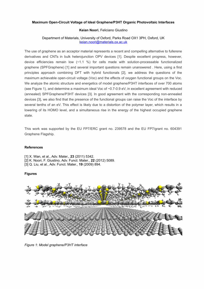
����������� �������������������������������������������������������������
!����"����������������� ��
�������������������� ������� ����������������� ��������� �!����������"����#��$�������� #�#��#��
%&��� ����'���&���� ������������������������� �� �������������������'����������������������
���������� ����()% � � �*����&����+�������,������� � -�.# ��� ���� ��������� ���'�� � �&/�����
������ � ���������� � ����� � �/ � 01�#� � 23 � �� � ���� � ���� � /��& � ����4���� �*�� � ��������5��
'���&���06������&��3�-�.���� ���������������7�� �� ��������� /�����#�!������ �'������ �
�������� � ������& � ��*��' ���% �/��& � &�*��� � ������� � -8.� � /� � ����� � �&� � 7�� �� � � � �&�
����������&����*�����4������������'��0,�3�����&�������� �����'����������'��� ���&��,�#
9������5���&�������� ���������������'���� ��������'���&��:� !%��������� �������;<<����
0 �����'�����3������������������������������,����1<#;4<#=��,��������������'�������/��&��������
0������3�6������&��:� !%������� �- .#�>�'���'�������/��&��&������ ���'�4������
������ �- .��/���� ������&����&����� �������&����������'��� ������� ���&��,�����&�����������*�
����������& ������,#�%&� ��������� ������������������ ��������&����������������/&��&��� ��� ����
�/���'����� �!���������������� �������� ��� �����&�����'�����&��&�'&� ����������'���&��
����#�
%&� �/���/� � ��������*���&��?����;:?�(�'����#�8 =@;A�����&��?����;:'����#�B<C =�
����&������' &��#
#����
-�.��#�9��������#��D��#������#��$��08<��3�@ C8#�-8.�"#�)�����#���� ����D��#�����#������#��$$�08<�83�@<A=#�- .�E#�F���������#��D��#�����#������#��%&�08<<=3�A=C#
'����
������������ ����������������������
Exfoliation of graphite to graphene for energy, water and biomedical applications
Shannon M Notley and Matthew D. J. Quinn
Faculty of Science, Engineering and Technology, Swinburne University of Technology, Hawthorn, VIC
3122, Australia [email protected]
Abstract The exfoliation of van der Waals bonded solids has been of great recent interest with the formation of graphene from graphite the most notable[1]. Other materials such as the transition metal dichalcogenides have received less attention however MoS2 and WS2 also display interesting properties in the limit of 2D[2, 3]. In principle, any layered solid material held together through weak dispersion forces can be exfoliated to single sheets[4] using a ran
assisted liquid phase exfoliation[5]. All of these techniques have advantages and limitations, indeed few are capable of generating large volumes of exfoliated sheets whilst maintaining sheet integrity. One method that shows great promise and can be scaled to meet industry needs is the aqueous based surfactant assisted liquid exfoliation technique[6]. Here, the properties of material such as graphene will be discussed as will potential applications of exfoliated surfactant stabilised sheets generated in this manner. Whilst complete removal of adsorbed surfactant from the graphene surface can be problematic in some applications, in others the presence of surfactant is a distinct advantage[7]. A particular focus of this presentation will be the interaction of light with graphene .All atoms and molecules within the material are freely available to absorb light upon exfoliation. Graphene absorbs strongly across the spectrum, particularly in the infrared region which makes it suitable as photothermal agents. Furthermore, forming into a film with exposed edges induces bactericidal action. The anti-bacterial activity of graphene films will also be discussed. References: 1. Geim, A.K., Graphene: Status and prospects. Science, 2009. 324: p. 1530-1534. 2. Splendiani, A., et al., Emerging photoluminescence in monolayer MoS2. Nano Lett., 2010. 10: p. 1271-1275. 3. Notley, S.M., High yield production of photoluminescent WS2 nanoparticles. J. Colloid Interface Sci., 2013. 396: p. 160-164. 4. Coleman, J.N., et al., Two-dimensional nanosheets produced by liquid exfoliation of layered materials. Science, 2011. 331: p. 568-571. 5. Cheng, C. and D. Li, Solvated Graphenes: An Emerging Class of Functional Soft Materials. Adv. Mater., 2013. 25: p. 13-30. 6. Notley, S.M., Highly concentrated aqueous suspensions of graphene through ultrasonic exfoliation with continuous surfactant addition. Langmuir, 2012. 28: p. 14110-14113. 7. Quinn, M. D. J.; Ho, H. N.; Notley, S. M., Aqueous dispersions of exfoliated molybdenum disulfide for use in visible light photocatalysis. ACS Applied Materials and Interfaces, DOI: 10.1021/am404161k.

Mesoscopic Conductance Fluctuations in Monolayer & Bilayer Graphene
T. Ouchi1, Y. Iso
1, A. Mahjoub
1, S. Suzuki
1, N. Aoki
1, J. P. Bird
2, D. K. Ferry
3, Y. Ochiai
1
1 Graduate School of Advanced Integration Science, Chiba University,
1-33 Yayoi-cho, Inage-ku, Chiba 263-8522, Japan
2 Departments of Electrical Engineering, University at Buffalo, Buffalo, New York 14260, USA
3 School of Electrical, Computer, and Energy Engineering, and Center for Solid State
Electronics Research, Arizona State University, Tempe, AZ 85287-5706
E-mail: [email protected]
Graphene as a material for investigations of mesoscopic physics has provided a new system for
fundamental investigations of quantum transport. Recent work in our group has demonstrated repro-
ducible conductance fluctuations, which, at first glance, appear reminiscent of the so-called universal
conductance fluctuations (UCF), known from the study of dirty metals since the 1980s. A quantitative
comparison has shown, however, that these fluctuations are in fact non-universal, since they violate the
ergodic hypothesis that provides the foundation for UCF theory [1,2]. Detailed numerical simulations
of quantum transport, which indicate that conductance fluctuations generated by sweeping Fermi en-
ergy is generally, have recently confirmed this breakdown not equivalent to those obtained when vary-
ing magnetic field [3]. Indeed, in the same study, it was even found that the amplitude of fluctuation is
dependent upon the amplitude of the random potential, in marked contrast to the expectations for UCF.
This violation of one of the core concepts of mesoscopic physics indicates that more work needs to be
done to understand the nature of quantum-interference phenomena in graphene. In our presentation
we therefore describe our recent low-temperature measurements of mesoscopic fluctuations in
graphene, in which we compare the amplitude of fluctuations arising from separate variation of either
magnetic field or Fermi energy. From a comparison of these different experiments, we discuss how the
influence of disorder is manifested in the non-universal conductance fluctuations of graphene.
1. G. Bohra et al., Phys. Rev. B 86, 161405(R) (2012).
2. G. Bohra et al., Appl. Phys. Lett. 101, 093110 (2012).
3. B. Liu, R. Akis, and D. K. Ferry, J. Phys.: Cond. Matt., in press.

Removal of residual PMMA on graphene surface by Infrared irradiation
Hye Min Oh, Doo Jae Park, Ji-Hee Kim, Young Hee Lee, Mun Seok Jeong*
Center for Integrated Nanostructure Physics (CINAP), Institute for Basic Science (IBS), Department of
Energy Science, BK21 Physics Division, and Center for Nanotubes and Nanostructured Composites,Sungkyunkwan University,Suwon 446-746, Korea
Contact [email protected]
Abstract
Large-area graphene was synthesized by chemical vapor deposition (CVD) growth on metal substrates.
The graphene has advantages such as extremely high carrier mobility, high thermal conductivity, low
resistivity.[1] Typically, poly(methyl methacrylate) (PMMA) is used when graphene transfer to other
substrates. The typical transfer process of CVD graphene includes spin coating with PMMA and then
etching the copper substrate with copper etchant. After the removal of copper, the PMMA-coated
graphene film is placed on the substrate. To remove PMMA on graphene, people used to dip the
graphene into the acetone. However, it is known that the remove of PMMA on the graphene is difficult to
completely using the acetone. This normally transfer process damages the graphene by inducing ripple
and crack formation. Also, the carboxyl functional group in PMMA on graphene surface is the source of
p-doping. Therefore, to remove the PMMA on the graphene surface, many research groups have
employed various methods such as the thermal treatment, and other solvent.[2,3] Nevertheless, a part
of PMMA still remain on graphene surface. Usually, to observe the residual PMMA on graphene surface,
topography of graphene surface scanned by atomic force microscopy is used. However, in that case, we
can not distinguish PMMA and other particles.
In this study, to confirm the residual PMMA on graphene surface, we employed novel measurement
technique which is available to distinguish PMMA and other particles by means of photothermal effect.
And we report removal of PMMA on graphene through IR irradiation. To confirm the residual PMMA on
graphene surface.
References
[1] Alexander N. obraztsov , Nature Nanotechnology. 4, 212 - 213 (2009)
[2] Lin, Y. C., Lu, C.C., Yeh, C. H., Jin, C., Suenaga, Kazu., and Chiu, P.W., Nano Lett. 2012, 12, 414-
419
[3] Jeong, H. Jin , Kim, H. Y , Jeong, S. Y, Han, J.T , Baeg, K. J, Hwang, J.Y , Lee, G.W, CARBON 66
( 2014 ) 612 618
Figure
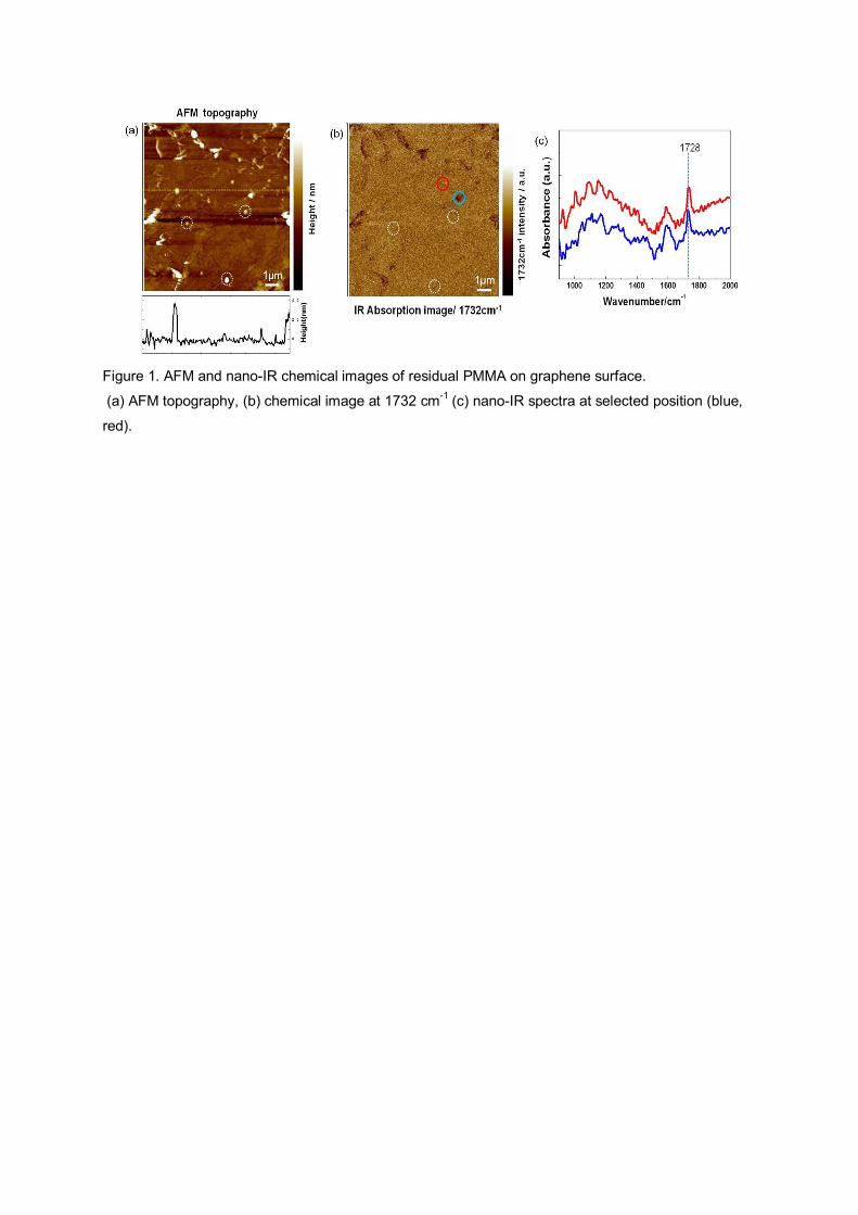
Figure 1. AFM and nano-IR chemical images of residual PMMA on graphene surface.
(a) AFM topography, (b) chemical image at 1732 cm-1 (c) nano-IR spectra at selected position (blue,
red).
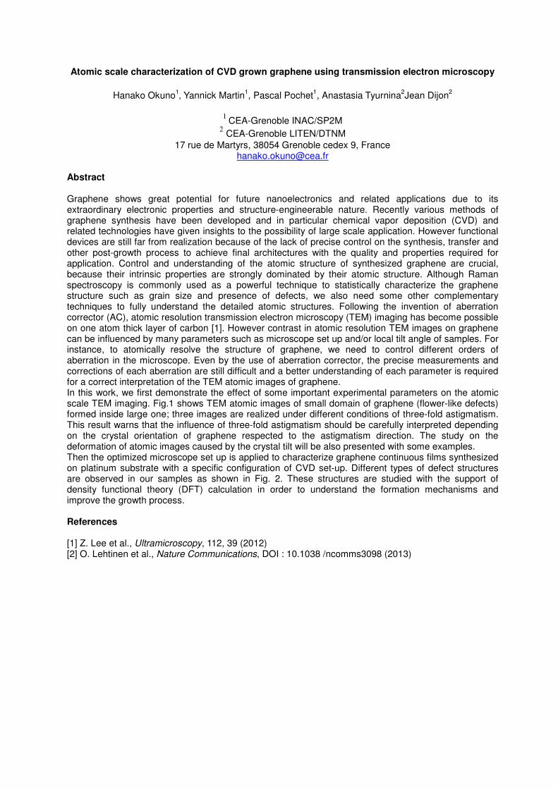
Atomic scale characterization of CVD grown graphene using transmission electron microscopy
Hanako Okuno1, Yannick Martin
1, Pascal Pochet
1, Anastasia Tyurnina
2Jean Dijon
2
1 CEA-Grenoble INAC/SP2M
2CEA-Grenoble LITEN/DTNM
17 rue de Martyrs, 38054 Grenoble cedex 9, France [email protected]
Abstract
Graphene shows great potential for future nanoelectronics and related applications due to its extraordinary electronic properties and structure-engineerable nature. Recently various methods of graphene synthesis have been developed and in particular chemical vapor deposition (CVD) and related technologies have given insights to the possibility of large scale application. However functional devices are still far from realization because of the lack of precise control on the synthesis, transfer and other post-growth process to achieve final architectures with the quality and properties required for application. Control and understanding of the atomic structure of synthesized graphene are crucial, because their intrinsic properties are strongly dominated by their atomic structure. Although Raman spectroscopy is commonly used as a powerful technique to statistically characterize the graphene structure such as grain size and presence of defects, we also need some other complementary techniques to fully understand the detailed atomic structures. Following the invention of aberration corrector (AC), atomic resolution transmission electron microscopy (TEM) imaging has become possible on one atom thick layer of carbon [1]. However contrast in atomic resolution TEM images on graphene can be influenced by many parameters such as microscope set up and/or local tilt angle of samples. For instance, to atomically resolve the structure of graphene, we need to control different orders of aberration in the microscope. Even by the use of aberration corrector, the precise measurements and corrections of each aberration are still difficult and a better understanding of each parameter is required for a correct interpretation of the TEM atomic images of graphene. In this work, we first demonstrate the effect of some important experimental parameters on the atomic scale TEM imaging. Fig.1 shows TEM atomic images of small domain of graphene (flower-like defects) formed inside large one; three images are realized under different conditions of three-fold astigmatism. This result warns that the influence of three-fold astigmatism should be carefully interpreted depending on the crystal orientation of graphene respected to the astigmatism direction. The study on the deformation of atomic images caused by the crystal tilt will be also presented with some examples. Then the optimized microscope set up is applied to characterize graphene continuous films synthesized on platinum substrate with a specific configuration of CVD set-up. Different types of defect structures are observed in our samples as shown in Fig. 2. These structures are studied with the support of density functional theory (DFT) calculation in order to understand the formation mechanisms and improve the growth process.
References
[1] Z. Lee et al., Ultramicroscopy, 112, 39 (2012) [2] O. Lehtinen et al., Nature Communications, DOI : 10.1038 /ncomms3098 (2013)

Figures
Fig. 1 AC-TEM images of small unit of graphene formed inside large one with three-fold astigmatism (a) 0 nm, (b) 200nm in 30° direction and (c) 200 nm in 60° direction. Low-pass filtered images are shown in red insets and simulated images are shown in blue insets together with used atomic model (red points). Scale bar is 2 nm.
Fig.2 AC-TEM low-pass Fourier filtered images of typical defect structures observed in graphene synthesized with our specific configuration of CVD set-up. Maximum filtered [2] images of defect structures indicated with red squires are shown on insets. Scale bar is 1 nm.

Bound states in the continuum with Dirac-like fermions
in trilayer graphene nanoribbons
N. Cortés1, Luis Rosales
1, M. Pacheco
1, L. Chico
2and P.A. Orellana
1
1Departamento de Física, Universidad Técnica Federico Santa María, Casilla 110V, Valparaíso, Chile,
2Departamento de Teoría y Simulación de Materiales, Instituto de Ciencia de Materiales de Madrid,
CSIC, 28049 Cantoblanco, Spain
Abstract
The new material denominated graphene is a single layer of carbon atoms, which can be fabricated by different methods like mechanical peeling or epitaxial growth [1]. Nanoribbons are stripes of graphene,which can be obtained through high-resolution lithography [2] by controlled cutting processes [3] or by unzipping multiwalled carbon nanotubes [4]. The electronic behavior of all these nanostructures is mainly determined by their geometric confinement, which allows the observation of quantum effects such as quantum interference effects, resonant tunneling and localization effects. The possibility to control these quantum effects, by applying external perturbations to the nanostructures or by modifying the geometrical confinement, could be used to develop new technological applications, such as graphene-based composite materials [5], molecular sensor devices [6] and nanotransistors [7].
An interesting feature of certain confined nanostructures is the presence of bound states in the continuum (BICs). The formation of BICs is a result of interference between quasi-stationary states via indirect coupling through the continuum. von Neumann and Wigner predicted the existence of BICs at the dawn of quantum mechanics by for certain spatially oscillating attractive potentials for a one-particle Schrödinger equation [8]. Bound states in the continuum have also shown to be present in electronictransport in mesoscopic structures. There are theoretical works showing the formation of these states in a four-terminal junction [9] and in a ballistic channel with intersections [10]. Until nowadays, there is only one experimental work, reported by Capasso and co-workers[11], in which BICs were measured in semiconductor heterostructures grown by molecular beam epitaxy. Thereby, the search of new systems, which could be able to reveal the existence of BICs and with the capability of do measurements of these states, is a very interesting and important field of research. In this sense, we believe that our findings indicate that trilayer graphene heterostructures are suitable systems to observe bound states in the continuum.
The experimental feasibility exhibited by graphene-based systems, the great advances in the controlled manipulation and measurements reported in graphene, and the feasibility of modified their electronic properties by apply external potentials, suggests that BICs could be observable in trilayer graphene nanoribbon.
In this work we study the formation of these exotic states with Dirac-like fermions in heterostructurescomposed by trilayer graphene nanoribbon. We identify the existence of bound states in the continuum in this system by means of the calculation of the local density of states and electronic conductance of the systems. We discuss the feasibility to observe the bound state in the continuum experimentally in this kind of system.
We focus on the properties of a system like the one depicted in Fig. 1, namely, an armchair nanoribbon of infinite length with two equal flakes of the same width as the ribbon, symmetrically placed above and below it. This can be viewed as three graphene flakes with AAA stacking with two contacts made of semi-infinite graphene nanoribbons of the same widths as the flakes.
References
[1] K. S. Novoselov, A. K. Geim, S. V. Morozov, D. Jiang, Y. Zhang, S. V. Dubonos, I. V. Grigorieva, and A. A. Firsov, Science 306, (2004), 666. [2] X. Li, X. Wang, L. Zhang, S. Lee, H. Dai, Science, 319, (2008), 1229.
[3] Lijie Ci et al Nano Res 1, (2008), 116.

[4] D. V. Kosynkin et al. Nature 458, (2009), 872.[5] S. Stankovich, D. A. Dikin, G. H. B. Dommett, K. M. Kohlhaas, E. J. Zimney, E. A. Stach, R. D. Piner, S. T. Nguyen and R. S. Ruoff, Nature 442, (2006), 282. [6] L. Rosales, M. Pacheco, Z. Barticevic, A. Latgé, and P. Orellana, Nanotechnology, 19, (2008), 065402. [7] C. Stampfer, E. Schurtenberger, F. Molitor, J. Gttinger, T. Ihn, and K. Ensslin, Nano Letters 8, (2008), 2378. [8] J. von Neumann and E. Wigner, Phys. Z. 30, (1929), 465. [9] R. L. Schult, H. W. Wyld, and D. G. Ravenhall, Phys. Rev. B 41, (1990), 12760. [10] Zhen-Li Ji and Karl-Frederik Berggren, Phys. Rev. B 45, (1992), 6652. [11] Federico Capasso, Carlo Sirtori, Jerome Faist, Deborah L. Sivico, Sung-Nee G. Chu and Alfred Y. Cho, Nature 358, (1992), 565.
Figure 1. - Schematic view of a hybrid system composed of an armchair nanoribbon of infinite length with two equal flakes of the same width as the ribbon, symmetrically placed above and below it.
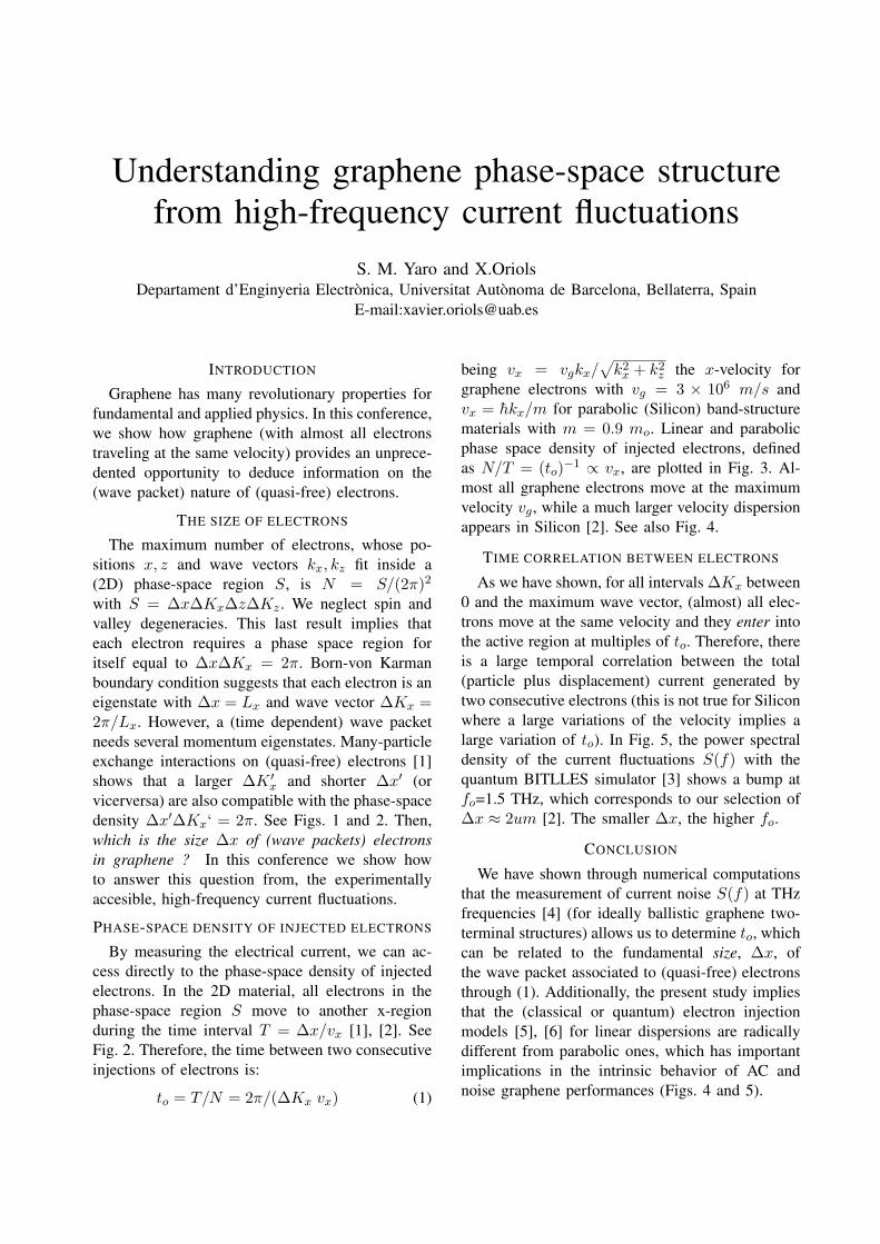
Understanding graphene phase-space structure
from high-frequency current fluctuations
S. M. Yaro and X.Oriols
Departament d’Enginyeria Electronica, Universitat Autonoma de Barcelona, Bellaterra, Spain
E-mail:[email protected]
INTRODUCTION
Graphene has many revolutionary properties for
fundamental and applied physics. In this conference,
we show how graphene (with almost all electrons
traveling at the same velocity) provides an unprece-
dented opportunity to deduce information on the
(wave packet) nature of (quasi-free) electrons.
THE SIZE OF ELECTRONS
The maximum number of electrons, whose po-
sitions x, z and wave vectors kx, kz fit inside a
(2D) phase-space region S, is N = S/(2π)2
with S = ∆x∆Kx∆z∆Kz . We neglect spin and
valley degeneracies. This last result implies that
each electron requires a phase space region for
itself equal to ∆x∆Kx = 2π. Born-von Karman
boundary condition suggests that each electron is an
eigenstate with ∆x = Lx and wave vector ∆Kx =2π/Lx. However, a (time dependent) wave packet
needs several momentum eigenstates. Many-particle
exchange interactions on (quasi-free) electrons [1]
shows that a larger ∆K ′
xand shorter ∆x′ (or
vicerversa) are also compatible with the phase-space
density ∆x′∆Kx‘ = 2π. See Figs. 1 and 2. Then,
which is the size ∆x of (wave packets) electrons
in graphene ? In this conference we show how
to answer this question from, the experimentally
accesible, high-frequency current fluctuations.
PHASE-SPACE DENSITY OF INJECTED ELECTRONS
By measuring the electrical current, we can ac-
cess directly to the phase-space density of injected
electrons. In the 2D material, all electrons in the
phase-space region S move to another x-region
during the time interval T = ∆x/vx [1], [2]. See
Fig. 2. Therefore, the time between two consecutive
injections of electrons is:
to = T/N = 2π/(∆Kx vx) (1)
being vx = vgkx/√
k2x+ k2
zthe x-velocity for
graphene electrons with vg = 3 × 10⁶ m/s and
vx = hkx/m for parabolic (Silicon) band-structure
materials with m = 0.9 mo. Linear and parabolic
phase space density of injected electrons, defined
as N/T = (to)−1
∝ vx, are plotted in Fig. 3. Al-
most all graphene electrons move at the maximum
velocity vg, while a much larger velocity dispersion
appears in Silicon [2]. See also Fig. 4.
TIME CORRELATION BETWEEN ELECTRONS
As we have shown, for all intervals ∆Kx between
0 and the maximum wave vector, (almost) all elec-
trons move at the same velocity and they enter into
the active region at multiples of to. Therefore, there
is a large temporal correlation between the total
(particle plus displacement) current generated by
two consecutive electrons (this is not true for Silicon
where a large variations of the velocity implies a
large variation of to). In Fig. 5, the power spectral
density of the current fluctuations S(f) with the
quantum BITLLES simulator [3] shows a bump at
fo=1.5 THz, which corresponds to our selection of
∆x ≈ 2um [2]. The smaller ∆x, the higher fo.
CONCLUSION
We have shown through numerical computations
that the measurement of current noise S(f) at THz
frequencies [4] (for ideally ballistic graphene two-
terminal structures) allows us to determine to, which
can be related to the fundamental size, ∆x, of
the wave packet associated to (quasi-free) electrons
through (1). Additionally, the present study implies
that the (classical or quantum) electron injection
models [5], [6] for linear dispersions are radically
different from parabolic ones, which has important
implications in the intrinsic behavior of AC and
noise graphene performances (Figs. 4 and 5).
Fig. 1. (a) The presence of N=9 electrons in a region of
the 1D phase-space implies that the probability P (Φ) of N=10
electrons inside the same region is almost zero. (b) Contour plot
of the right figure where each electron is separated a normalized
distance d from the rest [1]. Each electrons requires a phase
space region equal to 2π.
Fig. 4. Number of electrons as a function of instantaneous
current I they take during a simulation time of 1 ps at 100 K,
with Fermi energy Ef = 0.1 eV for (a) Silicon (b) Graphene.
Almost all graphene electrons move at the same velocity and
carry the same instantaneous current. This effect has important
implications in the intrinsic behavior of AC and noise graphene
performances [2], [4].
REFERENCES
[1] A. Alarcon, S. Yaro, X. Cartoixa, and X. Oriols Computa-
tion of many-particle quantum trajectories with exchange
interaction: Application to the simulation of nanoelectronic
devices Journal of Physics: Condensed Matter. 25, 325601
(2013).
[2] S.M.Yaro and X.Oriols, submitted.
[3] http://europe.uab.es/bitlles
[4] Kumada, N. et al. Plasmon transport in graphene in-
vestigated by time-resolved electrical measurements. Nat.
Commun. 4:1363(2013).
[5] X. Oriols, Quantum-trajectory approach to time-dependent
transport in mesoscopic systems with electron-electron
interactions Phys. Rev. Lett., 98, 066803 (2007).
[6] X.Oriols and D.K.Ferry Quantum transport beyond DC
Journal of Computational Electronics, 12(3), 317-330
(2013)
∆Z
∆x=Vx . τo
Vx
Lx
Lz
Reservoir ReservoirSimulation Box
GrapheneGrapheneGraphene
Fig. 2. Schematic representation of the (graphene) reservoir
and (graphene) active region of length Lx where the injection
of electrons (with constant rate) takes place.
Fig. 3. Number of injected electrons computed from Eq. (1)
as N/T = (to)−1 ∝ vx for each point of the 2D wave vector
space {kx, kz} during a simulation time of 1 ps at 100 K,
with Fermi energy Ef = 0.1 eV . (a) Silicon where highest
injection rate appears at highest energies, and vx does only
depend on {kx}. (b) Garphene where the highest injection
appears in almost all points {kx, kz}, except those with high
kz [2]. The velocity vx does explicitly depend on {kx, kz}.
1 100
100
200
300
400
500
600
Linear band Parabolic band
S(f
)(p
A2/H
z)
Frequency (THz)
300o
K
Fig. 5. Preliminary results with the quantum BITLLES simula-
tor [3] for the power spectral density of the current fluctuations
S(f) as a function of frequency f for the ideally ballistic
graphene two-terminal resistors of Fig. 1 with Lx=100 nm and
Lz=1 um with a Fermi level Ef = 0.05eV . The graphene
resistors (red) involves a higher cut-off frequency of S(f) than
Silicon one (black) because of a shorter current (particle and
displacement) pulses. The presence of the graphene (red) bump
at fo ≈ 1.5 THz (and other harmonics) is related to the time
to = 1/fo in Eq. (1).
Effect of zigzag and armchair edges on the electronic transport in single-layer and bilayer
graphene nanoribbons
Anna Orlof, Julius Ruseckas, Igor Zozoulenko
Linköping Univeristy, SE-581 83,Linköping Sweden [email protected]
We have studied the transmission properties of mono- and bilayer grapheme nanoribbons with defects
focusing on the role of the edge termination (zigzag vs armchair). Using the standard tight-binding
model of p-orbital electrons on a hexagonal lattice we have developed an analytical approach based on
the Green's function technique and the Dyson equation for calculation of the transmission coefficient of
monolayer grapheme nanoribbons with a single short-range defect. Calculation of the conductance
in monolayer graphene nanoribbons with many defects and calculations for bilayer graphene
nanoribbons are performed numerically on the basis of the tight-binding recursive Green's function
technique. The principal conclusions of our work (see [1]) can be summarized as follows:
1. For the case of the zigzag edge termination, both monolayer and bilayer nanoribbons in a
single- and a few-mode regime remain practically insensitive to defects situated close to the
edges (fig.1 (a), (c), fig.2 (a), (c)). This remarkable behavior is related to the effective boundary
condition at the zigzag edges which do not couple valleys, thus prohibiting the intervalley
scattering due to short-range defects situated close to the edges. In contrast, the armchair
edges mixes the valleys; as a result, the conductance of both monolayer and bilayer
nanoribbons is strongly affected by even a small defect concentration at the edges (fig.1 (b), (d),
fig.2 (b), (d)).
2. For higher electron energies in the many-mode regime, the difference of the transmission
between the armchair and zigzag ribbons diminishes and for sufficiently high defect
concentration they become equally sensitive to the edge disorder (fig. 2).
3. Both monolayer and bilayer nanoribbons with a short-range defect show resonant features in
the lowest energy mode (fig.1). Resonances are identified to be of Fano type and emerge from
the interference between the quasi-bound localized state around the defect and the extended
state in the ribbon. We consider four different cases of a defect in (a) zGNR, (b) zBGN, (c)
aGNR, and (d) aBGN. We discuss in detail how the interplay between the defects position at
different sublattices in the ribbons, defect distance to the edge and the structure of the extended
states in ribbons with different edge termination influence the width and the energy of Fano
resonances.
References
[1] A. Orlof, J. Ruseckas, I. V. Zozoulenko, Phys. Rev. B, 88 (2013) 125409.

Figures
Figure 1. Transmission of the monolayer (a),(b) and bilayer (c), (d) nanoribbons with a single defect at the edge as a function of the energy. Insets indicate defect positions and correspond to the curve color. Green curves indicate the transmission probability for ideal nanoribbons (without defects).
Figure 2. Transmission of monolayer (a), (b) and bilayer (c), (d) nanoribbons with disordered edges. Top insets illustrate two disorder models. Green curves indicate the transmission probability for ideal nanoribbons, red for nanoribbons with edge disorder of model p1, p2, p3 , the remaining curves are the result of the rectangular edge disorder sketched in the inset.

Nanoparticle-induced strain and nanoscale rippling in graphene
Z. Osváth1,3
, G. Molnár1, E. Gergely-Fülöp
1, A. Deák
1, N. Nagy
1, K. Kertész
1, P. Nemes-Incze
1,3, X.
Jin2,3
, C. Hwang2,3
, and L. P. Biró1,3
1Institute of Technical Physics and Materials Science, MFA, Research Centre for Natural Sciences, P.O.
Box 49, 1525 Budapest, Hungary (http://www.nanotechnology.hu) 2Center for Nano-metrology, Division of Industrial Metrology, Korea Research Institute of Standards and
Science, Yuseong, Daejeon 305-340, Republic of Korea 3Korean-Hungarian Joint Laboratory for Nanosciences (KHJLN), P.O. Box 49, 1525 Budapest, Hungary
Abstract
Atomically thin graphene membranes are intrinsically non-flat and have random or quasi-periodic corrugations at the nanometer scale [1, 2]. Since this is closely affecting the electronic properties, there is an increasing need for the realization of graphene sheets with controlled corrugation. Substrates play a crucial role, as the graphene substrate interaction can impart an extrinsic rippling to graphene which differs from its intrinsic corrugation [3, 4]. Such rippling can contribute to the scattering of charge carriers [5, 6]. In order to preserve the high carrier mobility needed for nanoelectronic applications, atomically flat mica [7] and hexagonal boron nitride [8] substrates were introduced recently, which reduce charge inhomogeneity [9] and smooth out corrugations in graphene leading to ultra-flat morphology. On the other hand, corrugated graphene can be good candidate for sensor applications, as recent simulations [10, 11] predict enhanced chemical activity in rippled graphene. The crests and troughs of graphene ripples form active sites for the adsorption of different molecules. It was proposed based on first-principles calculations [12] that this can open a way for tunable, regio-selective functionalization of graphene. The extrinsic rippling can be induced for example by pre-prepared elastic substrates [13] or silica nanoparticles (NPs) [14], a possibility which has not been fully explored yet experimentally [15].
In this work we investigate by atomic force microscopy (AFM) the properties of CVD-grown graphene transferred onto a continuous layer of SiO2 NPs with diameters of around 25 nm, prepared on Si substrate by Langmuir-Blodgett technique (Figure 1). We show that the extrinsic graphene rippling can be controlled by annealing at moderate temperatures (400
oC). Confocal Raman microscopy
(WITec) revealed that annealing increases doping and introduces compressive strain into the atomically thin membrane (Figure 2).
Due to the high nanoparticle density, graphene membranes remain completely detached from the Si substrate. The membrane parts bridging the nanoparticles are suspended, as revealed by both AFM topographic and phase images, and can be reversibly lifted by the attractive forces between an atomic force microscope tip and graphene. Such dynamic control of the local graphene morphology can play an important role in the development of graphene based nanomechanical devices such as switches [16, 17]. Local indentation experiments were performed on the suspended parts in order to investigate the elastic properties of the graphene membrane. References [1] A. Fasolino, J.H. Los, M.I. Katsnelson, Nat. Mater. 6 (2007) 858. [2] J.C. Meyer, A.K. Geim, M.I. Katsnelson, K.S. Novoselov, T.J. Booth, S. Roth, Nature 446 (2007) 60. [3] M. Ishigami, J.H. Chen, W.G. Cullen, M.S. Fuhrer, E.D. Williams, Nano Lett. 7 (2007) 1643. [4] V. Geringer, M. Liebmann, T. Echtermeyer, S. Runte, M. Schmidt, R. Rückamp, M.C. Lemme, M. Morgenstern, Phys. Rev. Lett. 102 (2009) 076102. [5] M.I. Katsnelson, A.K. Geim, Phil. Trans. R. Soc. A 366 (2008) 195. [6] G.-X. Ni, Y. Zheng, S. Bae, H.R. Kim, A. Pachoud, Y.S. Kim, C.-L. Tan, D. Im, J.-H. Ahn, B.H. Hong, B. Özyilmaz, ACS Nano 6 (2012) 1158. [7] C. Lui, L. Liu, K. Mak, G. Flynn, T. Heinz, Nature 462 (2009) 339. [8] C.R. Dean, A.F. Young, I. Meric, C. Lee, L. Wang, S. Sorgenfrei, K. Watanabe, T. Taniguchi, P. Kim, K.L. Shepard, J. Hone, Nat. Nanotechnol. 5 (2010) 722. [9] R. Decker, Y. Wang, V.W. Brar, W. Regan, H.-Z. Tsai, Q. Wu, W. Gannett, A. Zettl, M.F. Crommie, Nano Lett. 11 (2011) 2291. [10] D.W. Boukhvalov, M.I. Katsnelson, J. Phys. Chem. C 113 (2009) 14176. [11] D.W. Boukhvalov, Surf. Sci. 604 (2010) 2190. [12] X. Gao, Y. Wang, X. Liu, T.-L. Chan, S. Irle, Y. Zhao, S.B. Zhang, Phys. Chem. Chem. Phys. 13 (2011) 19449.
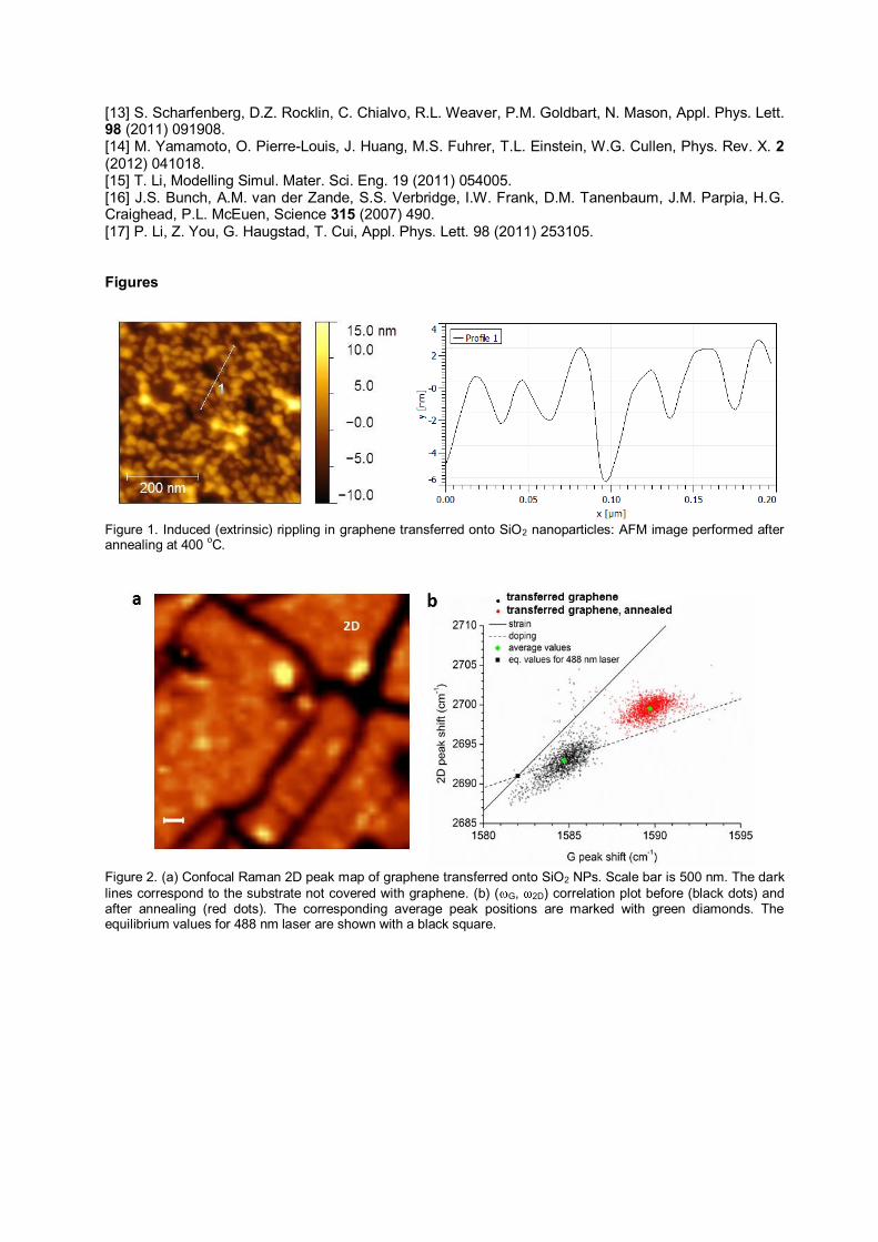
[13] S. Scharfenberg, D.Z. Rocklin, C. Chialvo, R.L. Weaver, P.M. Goldbart, N. Mason, Appl. Phys. Lett. 98 (2011) 091908. [14] M. Yamamoto, O. Pierre-Louis, J. Huang, M.S. Fuhrer, T.L. Einstein, W.G. Cullen, Phys. Rev. X. 2 (2012) 041018. [15] T. Li, Modelling Simul. Mater. Sci. Eng. 19 (2011) 054005. [16] J.S. Bunch, A.M. van der Zande, S.S. Verbridge, I.W. Frank, D.M. Tanenbaum, J.M. Parpia, H.G. Craighead, P.L. McEuen, Science 315 (2007) 490. [17] P. Li, Z. You, G. Haugstad, T. Cui, Appl. Phys. Lett. 98 (2011) 253105. Figures
Figure 1. Induced (extrinsic) rippling in graphene transferred onto SiO2 nanoparticles: AFM image performed after annealing at 400
oC.
Figure 2. (a) Confocal Raman 2D peak map of graphene transferred onto SiO2 NPs. Scale bar is 500 nm. The dark
lines correspond to the substrate not covered with graphene. (b) ( G, 2D) correlation plot before (black dots) and after annealing (red dots). The corresponding average peak positions are marked with green diamonds. The equilibrium values for 488 nm laser are shown with a black square.

Non-covalent Interactions of Small Organic Molecules To Graphene: Theory and Experiment
Michal Otyepka, Eva Otyepková, Kocman
Regional Centre of Advanced Technologies and Materials, Department of Physical Chemistry, Faculty
of Science, Palacky University Olomouc, Czech Republic [email protected]
Abstract Graphene is a two- -conjugated material having extraordinary physical properties, which makes its a perspective material in catalysis, energy storage, nano(opto)electronics and sensor applications.[1,2] The application potential of graphene can be enormously enhanced by its covalent and non-covalent functionalization.[3] An exact quantification of interaction between graphene and guest molecules as well as thorough understanding of the nature of interaction between graphene and guest molecules have not been yet achieved. We measured the adsorption enthalpies of acetone, acetonitrile, dichloromethane, ethanol, ethyl acetate, hexane, and toluene vapours on graphene by inverse gas chromatography. The measured adsorption enthalpies
We compared the experimental data with theoretical calculations at density functional theory (PBE, B97D, M06-2X, and optB88-vdW), wave function theory (MP2, SCS(MI)-MP2, MP2.5, MP2.X, and CCSD(T)), and empirical (OPLS-AA) levels using two graphene models: coronene and infinite graphene (using periodic boundary conditions). We also employed symmetry-adapted perturbation theory (SAPT) calculations to understand the nature of interaction between graphene model (coronene) and the organic molecules. SAPT calculations showed that the interactions were governed by London dispersive forces (amounting to 60% of attractive interactions), even for the polar molecules. The theoretical calculations also showed that the adsorption enthalpies were largely controlled by the interaction energy. Adsorption enthalpies obtained from ab initio molecular dynamics employing non-local optB88-vdW functional were in excellent agreement with the experimental data, indicating that the functional can cover physical phenomena behind adsorption of organic molecules on graphene sufficiently well.[4] We further used theoretical calculations to understand changes in adsorption enthalpies of acetone to graphene and graphite with surface coverage. References [1] Novoselov KS et al. Science 306, (2004) 666. [2] Novoselov KS et al. Nature 490, (2012) 192. [3] Georgakilas V et al. Chem. Rev. 112, (2012) 6156. [4] Lazar P et al. J. Am. Chem. Soc. 135, (2013) 6372.

Tunable gap in bilayer beta-graphyne
M. Pacheco1, A. León
2
1Universidad Santa María, Avda España 1680, Valparaíso, Chile
2Universidad Diego Portales, Ejército 441, Santiago, Chile
Abstract
Among the large variety of carbon allotropes there are graphene-like structures which can be
constructed by replacing some bonds =C = C = in graphene by acetylenic linkages - C ≡ C -, called
graphynes (GYs) [1], or by diacetylenic linkages - C ≡ C - C ≡ C, called graphdiynes (GDYs) [2]. Thesenon-natural carbon allotropes include both, sp
2- and sp
1-hybridized carbon atoms. After the theoretical
prediction of these flat structures, with exceptional electronic, thermal and mechanical properties,several experimental studies have been performed to achieve their large-scale synthesis [3]. Due to their intrinsic semiconducting properties, GYs and GDYs have been proposed as promising candidates in many electronic and photoelectronic applications and also with potential applications as membranes to separate molecules, hydrogen storage media, and anode materials in lithium-ion batteries [4,5].According to first-principles calculations [6] some particular types of graphynes-like networks possess
Dirac cones, as the case of graphene. One of these structure the so-called β-graphyne, has a Dirac
cone not located at the K and K’ points of the Brillouin zone but on lines between the high symmetry Γand M points. In this work we show a theoretical study based on DFT of the electronic properties of
bilayers of β-graphyne, for different stacking configurations. In Fig. 1 it is shown a scheme of the β-graphyne and the unit cell with the different stacking considered. Our results show that the bilayer is semimetal or semiconductor, depending on the staking mode. The system changes from a metal, for A-A stacking, to a semiconductor with a small gap of 0.15 eV for A-B stacking, being this most stable configuration according to the study of total energy and stability (Fig.2).By applying an electric field perpendicular to the layers, the gap of semiconductors can be closed and a
metallic state is obtained (Fig.3). This behavior is contrary to that reported for the case of α-graphyne [7]for which the semi-metallic systems become semiconductor with a gap that increases with the field intensity.
References
[1] Baughman RH, Eckhardt H, Kertesz M, J Chem Phys, 87 (1987) 6687.[2] M. M. Haley, S. C. Brand and J. J. Pak, Angew. Chem., Int. Ed. Engl., 36 (1997) 836.[3] G. Li, Y. Li, H. Liu, Y. Guo, Y. Li and D. Zhu, Chem. Commun., 46 (2010) 3256.[4]Ivanovskii A. L. Progress in Solid State Chemistry 41 (2013) 1.[5] Tang Q, Zhou Z, Chen Z. Nanoscale, 5 (2013) 4541.[6] Malko D, Neiss C, Vines F, Gorling A. Phys. Rev. Lett., 108 (2012) 086804.[7] O. Leenaerts, B. Partoens, and F. M. Peeters, Applied Physics Letters 103 (2013) 013105.
Figures
Fig.1 Scheme of a β-graphyne
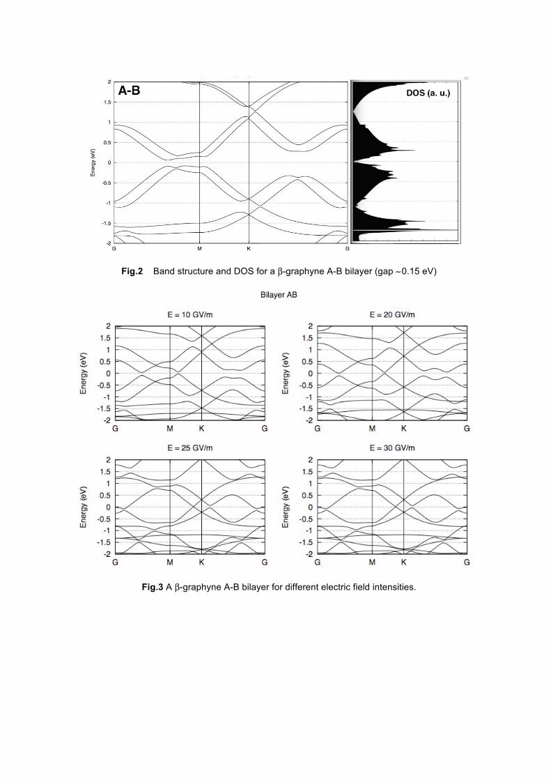
Fig.2 Band structure and DOS for a β-graphyne A-B bilayer (gap ∼0.15 eV)
Fig.3 A β-graphyne A-B bilayer for different electric field intensities.

Fragmentation and exfoliation of low-dimensional materials; a statistical approach.
Konstantinos Kouroupis-Agalou1, Andrea Liscio
1, Emanuele Treossi,
1,2 Luca Ortolani
3, Vittorio Morandi
3,
Nicola Maria Pugno4, Vincenzo Palermo
1,2*
1Istituto per la Sintesi Organica e la Fotoreattività-Consiglio Nazionale delle Ricerche (ISOF-CNR), via
Gobetti 101, 40129 Bologna, Italy.2Laboratorio MIST.E-R Bologna, via Gobetti 101, 40129 Bologna
(Italy)3
Istituto per la Microelettronica e Microsistemi-Consiglio Nazionale delle Ricerche (IMM-CNR),
via Gobetti 101, 40129 Bologna, Italy.4
Dipartimento di Ingegneria Civile, Ambientale e Meccanica,
Università di Trento, via Mesiano, 77 I-38123 Trento (Italia)
Abstract
A main advantage for applications of Graphene and related 2-dimensional materials is that they can be
produced on large scales by liquid phase exfoliation. The exfoliation process shall be considered as a
particular fragmentation process, where the 2-dimensional (2D) character of the exfoliated objects will
influence significantly fragmentation dynamics as compared to standard materials. Here, we used
automatized image processing of Atomic Force Microscopy (AFM) data to measure, one by one, the
exact shape and size of thousands of nanosheets obtained by exfoliation of an important 2D-material,
Boron Nitride, and used different statistical functions to model the asymmetric distribution of nanosheets
sizes typically obtained. Being the resolution of AFM much larger than the average sheet size, analysis
could be performed directly at the nanoscale, and at single sheet level. We find that the size distribution
of the sheets at a given time follows a log-normal distribution, indicating that the exfoliation process has
a “typical” scale length that changes with time and that exfoliation proceeds through the formation of a
distribution of random cracks that follow Poisson statistics.
References
[1] Xia, Z.Y.; G. Giambastiani; C. Christodoulou; M.V. Nardi; N. Koch; E. Treossi; V. Bellani; S. Pezzini; F.
Corticelli; V. Morandi; A. Zanelli; V. Palermo ChemPlusChem, (2014) DOI: 10.1002/cplu.201300375
[2] Schlierf, A.; P. Samori; V. Palermo Journal of Materials Chemistry C, (2014) DOI: 10.1039/C3TC32153C
[3] Xia, Z.Y.; S. Pezzini; E. Treossi; G. Giambastiani; F. Corticelli; V. Morandi; A. Zanelli; V. Bellani; V. Palermo
Advanced Functional Materials, 23 (2013) 4756
[4] Schlierf, A.; H.F. Yang; E. Gebremedhn; E. Treossi; L. Ortolani; L.P. Chen; A. Minoia; V. Morandi; P.
Samori; C. Casiraghi; D. Beljonne; V. Palermo Nanoscale, 5 (2013) 4205
[5] Russier, J.; E. Treossi; A. Scarsi; F. Perrozzi; H. Dumortier; L. Ottaviano; M. Meneghetti; V. Palermo; A.
Bianco Nanoscale, 5 (2013) 11234
[6] Palermo, V. Chemical Communications, Emerging investigators special issue, 49 (2013) 2848
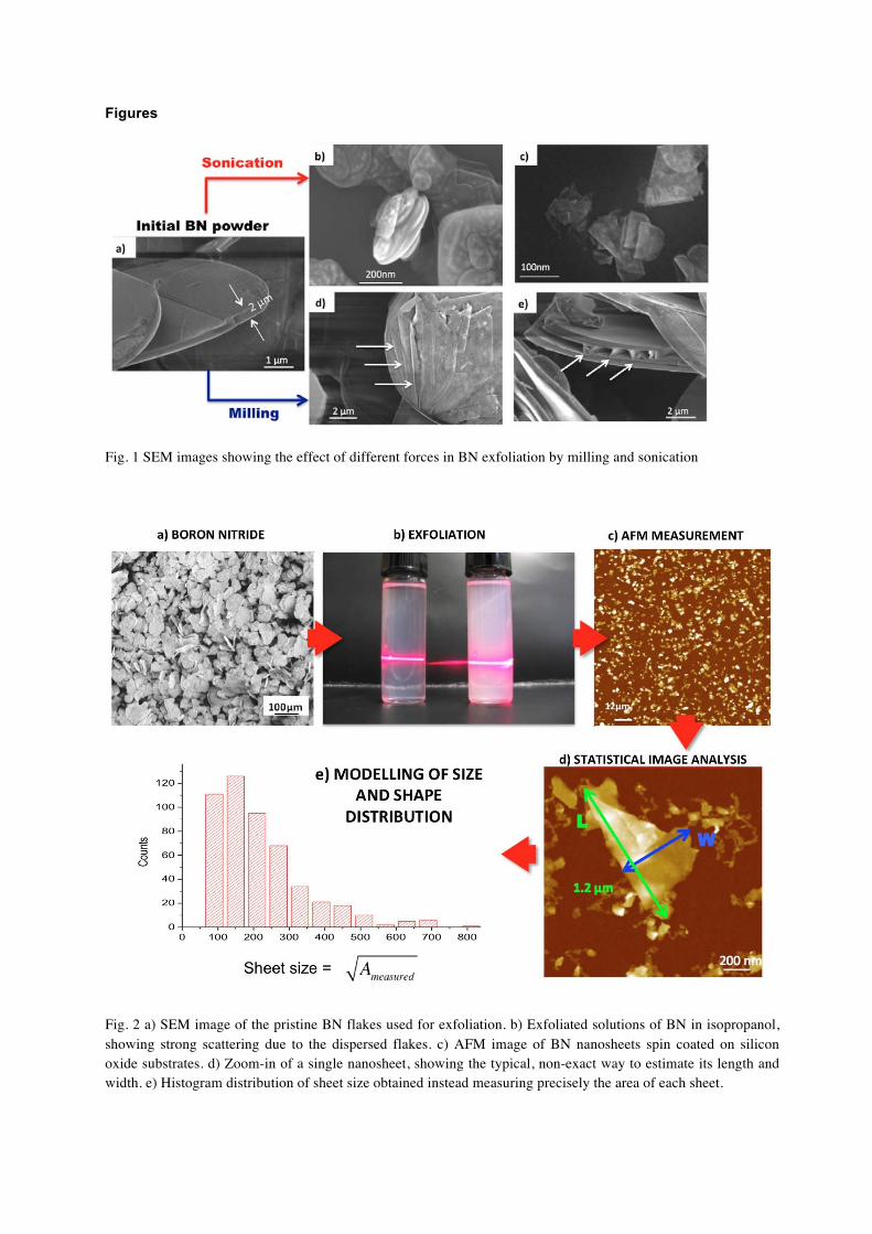
Figures
Fig. 1 SEM images showing the effect of different forces in BN exfoliation by milling and sonication
Fig. 2 a) SEM image of the pristine BN flakes used for exfoliation. b) Exfoliated solutions of BN in isopropanol,
showing strong scattering due to the dispersed flakes. c) AFM image of BN nanosheets spin coated on silicon
oxide substrates. d) Zoom-in of a single nanosheet, showing the typical, non-exact way to estimate its length and
width. e) Histogram distribution of sheet size obtained instead measuring precisely the area of each sheet.

First principles simulations of inelastic tunnel spectroscopy on graphene
Mattias Palsgaard, Nick Papior Andersen, Mads Brandbyge
Dept. of micro and nanotechnology & Center for Nanostructured Graphene (CNG), Tech. Univ. of Denmark (DTU), build. 345 east, 2800 Kongens Lyngby, Denmark
Experiments employing electron inelastic tunnel spectroscopy (IETS) performed using scanning tunnel microscopy(STM) on pristine graphene has revealed the importance of electron-phonon interactions in STM on graphene[1,3]. However, IETS can in principle also be a powerful tool for obtaining local information about defects such as adsorbates or grain boundaries. Here we present first principles calculations based on density functional theory (DFT) and non-equilibrium Greens functions in order to investigate how IETS can yield local information. Unique to graphene [1-3] the experimental results show a very prominent conductance gap in the tunneling spectra (tunnelling conductance vs. voltage). These spectra have been obtained depending on gate voltage, and the inelastic electron-phonon scattering mechanism has been established through a tight binding approach [4]. We perform first principles transport calculations using the TranSIESTA code in conjunction with SIESTA [5,6] (Fig 1a). Electronic coupling to the vibrations in graphene is included, with a lowest (second) order expansion of the self-consistent Born approximation [7,8]. We first demonstrate how these results on pristine graphene at different gate voltages can be reproduced using our methods for a suspended graphene sheet (Fig. 1b). We find that the conductance gap is independent of change in the gate voltage and increase of the tunnelling distance, as in experiments [1]. We then test the stability of the gap feature with respect to various modifications of the pristine graphene lattice. We find that hydrogen adsorbates on the graphene lattice quenches the gap feature locally, due to the introduction of short range protrusions. This effect is seen for hydrogenation on either side of the graphene sheet (Fig 1c). Near a hydrogen passivated armchair edge, the gap is also quenched. This should lead to local conductance enhancement near edges at low bias energy that cannot be attested to localized electronic states. In the presence of a Stone-Wales defect we find that the gap is only altered slightly due to low energy out-of-plane phonon modes. The low energy modes are a result of the instability of graphene near defect sites which can be related to long-range out-of-plane corrugations of graphene. Thus IETS may yield information about the local vibrational structure and instabilities towards corrugation. References [1] Y. Zhang, V. W. Brar, F. Wang, C. Girit, Y. Yayon, M. Panlasigui, A. Zettl, and M. Crommie, Nat. Phys., 4 (2008) 627. [2] Regis Decker, Yang Wang, Victor W. Brar, William Regan, Hsin-Zon Tsai, Qiong Wu, William Gannett, Alex Zettl, and Michael F. Crommie, Nano Lett., 11 (2011) 2291. [3] Victor W. Brar, Yuanbo Zhang, and Yossi Yayon, Appl. Phys. Lett., 91 (2007) 122102. [4] T. O. Wehling, I. Grigorenko, A. I. Lichtenstein, and A. V. Balatsky, Phys. Rev. Lett., 101 (2008) 216803. [5] J. M. Soler, E. Artacho, J. D. Gale, A. García, J. Junquera, P. Ordejón, and D. Sánchez-Portal, J. Phys.: Condens. Matter 14, 2745 (2002) [6] M. Brandbyge, J. L. Mozos, P. Ordejón, J. Taylor, and K. Stokbro, Phys. Rev. B 65, 165401 (2002) [7] T. Frederiksen, M. Paulsson, M. Brandbyge, A.-P. Jauho, Phys. Rev. B, 75, 205413 (2007) [8] J.-T. Lü, R.B. Christensen, G. Foti, T. Frederiksen, T. Gunst, and M. Brandbyge, Phys. Rev. B 89, 081405 (2014).

a)
b)
c)
Fig 1: (a) System setup with semi-infinite leads on both graphene ends and a model STM made of a 4 atom gold cluster (b) Differential conductance spectrum for: Experimental results, fitted to the principal axis (red) [1], dI/dV calculation of STM on pristine graphene (black) and graphene hydrogenated system (blue). (c) Graphene with hydrogen impurity.
Experiment
Adsorbed hydrogen
Calculation

Friction of few layer graphene over different substrates
Manoj Tripathi1,2
Guido Paolicelli2, Nicola Pugno
3,4,5 and Sergio Valeri
1,2
1Dipartimento di Scienze Fisiche Informatiche e Matematiche (FIM), Università di Modena e Reggio
Emilia, Via Campi 213 Modena, Italy 2CNR, Istituto Nanoscienze, Centro S3, Via Campi 213/A, 41125 Modena, Italy
3Laboratory of Bioinspired and Graphene Nanomechanics, Department of Civil Environmental and
Mechanical Engineering, University of Trento, Via Mesiano, 77, 38123 Trento, Italy. 4Center for Materials and Microsystems,Fondazione Bruno Kessler, I-38123 Trento, Italy
5School of Engineering and Materials Science, Queen Mary University of London, Mile End Road,
London, E1 4NS, UK
Contact: [email protected]
Abstract Nanoscale friction properties of chemical vapor deposition (CVD) grown graphene on polycrystalline Ni (Gr/Ni) with respect to mechanical exfoliated graphene deposited on SiO2 (Gr/SiO2) have been studied by Atomic Force Microscopy (AFM). These two types of graphene films possess rather different tribological characteristics. Micron scale, single domain flakes with very low defects and random variable thickness from single layer to thick graphite are routinely obtained by mechanical exfoliation of graphite crystal and are considered a standard for scientific application [1]. On the contrary, for large scale applications, the CVD grown graphene on polycrystalline metal is considered one of the more interesting method. Films obtained with this procedure are continuous over areas as large as few square centimeters but consist of a large number of graphene domains of few layer thickness separated by disordered regions [2]. Recently, friction experiments at micro scale have shown that Gr/Ni systems possess a lower friction coefficient with respect to Gr/SiO2 [3]. These measurements average out the contribution of graphene domains and disordered regions where nucleation has taken place. In order to elucidate the relative contribution of these regions, we performed AFM friction measurement at nanoscale in ambient and vacuum conditions (10
-5 Torr). We observed that the major contribution for reducing lateral force comes
from the disordered regions rather than the flat graphene domains, Fig. 1. We also perform nanoscale measurement on Gr/SiO2 flakes. Our results confirm that a single graphene layer is sufficient to strongly reduce (about 50 times) the friction with respect to bare SiO2, but also that friction decreases with increasing film thickness [4]. That is the friction is higher on single-layer region than respect to a bi-layer region and further decreases up to 3-4 layer thickness. We observe this trend both in air and vacuum conditions (10
-5 Torr), Fig. 2.
These results point out that properties of few layer graphene as a solid lubricant are dictated by both interaction with the supporting substrate and interlayer mechanical characteristics. Extending [5], a model for rationalizing the observations is also proposed. References [1] Novoselov K. S., Jiang D., Schedin F., Booth T. J., Khotkevich V. V., Morozov S. V., Geim A. K., PNAS, 102 (2005) 10451. [2] Huang P.Y., Vargas C. S. R., Zande A. M. V., Whitney W. S., Levendorf M. P., Kevek J. W., Garg S., Alden J. S., Hustedt C. J., Zhu Y., Park J., McEuen P. L., Muller D. A., Nature latter, 469 (2011) 389. [3] Kwang-Seop Kim H-JL, Changgu Lee, Seoung-Ki Lee, Houk Jang,Jong-Hyun Ahn, Jae-Hyun Kim, and Hak-Joo Lee. ACS Nano 5 (2011) 5107. [4] Lee C., Li Q., Liu W. K. X.-Z., Berger H., Carpick R. W., Hone J., Science, 328, (2010) 76. [5] Pugno N. M., Yin Q., Shi X., Capozza R., Meccanica, 48, (2013) 1845.
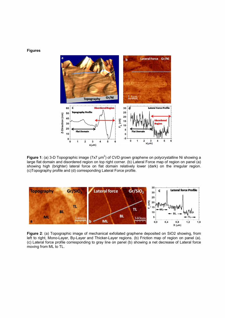
Figures
Figure 1: (a) 3-D Topographic image (7x7 µm
2) of CVD grown graphene on polycrystalline Ni showing a
large flat domain and disordered region on top right corner. (b) Lateral Force map of region on panel (a) showing high (brighter) lateral force on flat domain relatively lower (dark) on the irregular region. (c)Topography profile and (d) corresponding Lateral Force profile.
Figure 2: (a) Topographic image of mechanical exfoliated graphene deposited on SiO2 showing, from left to right, Mono-Layer, By-Layer and Thicker-Layer regions. (b) Friction map of region on panel (a). (c) Lateral force profile corresponding to gray line on panel (b) showing a net decrease of Lateral force moving from ML to TL.
Efficient mechanical loading of few layer graphene flakes: experiment and modeling
Georgia Tsoukleri
1, Charalampos Androulidakis
1, Nikos Delikoukos
1, John Parthenios
1, Aris Sgouros
2,
George Kalosakas1,2
, Costas Galiotis1,2
and Konstantinos Papagelis1,2
1Foundation of Research and Technology Hellas, Institute of Chemical Engineering and High
Temperature Processes, P.O. Box 1414, GR-26504 Patras (Greece) 2Department of Materials Science, University of Patras, GR-26504 Patras (Greece)
Abstract Recently, there has been a growing interest in trilayer and few layer graphene materials because of their interesting properties. In these systems the electronic, optical and vibrational properties are distinct from those of single-layer graphene and strongly depended on the crystallographic stacking of the individual graphene sheets providing an alternative degree of freedom to tune graphene properties [1]. Trilayers exhibit two main stacking order configurations, namely the energetically more stable Bernal (or ABA) and the rhombohedral (or ABC) stacking [2]. The ABA stacked trilayers are semimetals showing overlapping linear and quadratic electronic dispersion near the Fermi level with an electrically tunable band overlap, while ABC stacked trilayers are predicted to be semiconductors exhibiting cubic dispersion with a tunable band gap similar to that of bilayer graphene. Raman spectroscopy has been proven a very successful technique to investigate the effect of mechanical deformation on graphene materials under uniaxial tension and compression [3, 4, 5] or hydrostatic pressure [6]. Therefore, monitoring optical phonons it seems the clearest and simplest way to quantify the macroscopic stress/strain imparted to graphene sheets. In this work, we have been subjecting to tension various single-, bi-, tri- and few-layer graphene samples, embedded into the upper surface of a PMMA cantilever and covered by a ~100nm thickness polymeric film, while their Raman spectrum is recorded simultaneously. The mechanical response is monitored by the shift of the G and 2D Raman lines with strain, using the 785nm (1.58 eV) excitation wavelength. The investigated samples exhibit a notable peculiarity where each graphene unit does not form a stack having ideally sharp edges in the atomic scale. The single layer graphene (1LG) is in direct contact with the polymer substrate which is the footprint of the whole unit. The other layers forming the bilayer (2LG), trilayer (3LG) and few layer graphene (FLG) are extended above the monolayer partially overlapping in a ladder-like fashion (figure 1). We have observed for the first time the strain induced lifting of the degeneracy of the E2g mode in 3LG and FLG. The shift rates are similar to those observed for single and bilayer graphene [5]. The only difference is an up-shift of the onset of splitting due to the full width of half maximum enhancement with the number of layers. This behaviour indicates an efficient stress transfer across the graphene-polymer interface. On the other hand, for 3LG and FLG a linear dependence between the 2D Raman frequency and strain is observed. The 2D strain sensitivity in both cases is about 55 cm
-1/%. The results are different from
those of Gong et al [7] where they observed smaller 2D band shift rates (47 cm-1
/% for 3LG and 40 cm-
1/% for FLG) attributed to poor stress transfer efficiency upon increasing the number of layers. The
measured slopes of the studied samples show negligible dependence on the number of graphene layers as a consequence of the morphology of the studied sample where each internal graphene layer can be uniaxially loaded due to the direct contact with the polymer molecules. Molecular dynamics simulations using an improved long-range reactive bond-order potential for carbon (LCBOP) [8] with the long-range interactions cutoff at 0.6 nm to ensure interplanar binding in graphite have shown that for 3LG the middle layer can sustain tensile strains only up to 0.06% external strain before sliding. Besides, if 20% of the middle layer edge atoms located on both sides perpendicular to the uniaxial strain axis experience the applied force then the middle layer follow the induced deformation with efficiency of almost 85%. Therefore, in the case of embedded graphene flakes where the inner layers protruding from the upper and lower ones the interaction of the uncovered parts of the flake with the polymer matrix can enhance dramatically the load transfer from the matrix to the inclusions. The observed behavior have important implications in the level of reinforcement in polymer composites where we can engineer the degree of reinforcing efficiency for few layer graphene or even nano-graphite by suitably shaping the edges of the inner graphene layers. References

[1] K. Kim, S. Coh, L. Z. Tan, W. Regan, J. M. Yuk, E. Chatterjee, M. F. Crommie, M. L. Cohen, S. G. Louie, and A. Zettl, Physical Review Letters, 108 (2012) 246103. [2] C. H. Lui, Z. Li, Z. Chen, P. V. Klimov, L. E. Brus and T. F. Heinz, Nano Letters, 11 (2011) 164. [3] G. Tsoukleri, J. Parthenios, K. Papagelis, R. Jalil, A. C. Ferrari, A. K. Geim, K. S. Novoselov and C. Galiotis, Small, 21, (2009) 2397. [4] O. Frank G. Tsoukleri, J. Parthenios, K. Papagelis, I. Riaz, R. Jalil, K. S. Novoselov and C. Galiotis, ACS-Nano, 4, (2010) 3131. [5] Papagelis and C. Galiotis, Nano Letters, 12, (2012) 687. [6] K. Filintoglou, N. Papadopoulos, J. Arvanitidis, D. Christofilos, O. Frank, M. Kalbac, J. Parthenios, G. Kalosakas, C. Galiotis and K. Papagelis, Physical Review B, 88, (2013) 045418-1-6. [7] L. Gong, R. J. Young, I. A. Kinloch, I. Riaz, R. Jalil and K. S. Novoselov, ACS Nano, 6, (2012) 2086. [8] J. H. Los, L. M. Ghiringhelli, E. Jan Meijer, and A. Fasolino, Physical Review B, 72, (2005) 214102. Figures
0,0 0,2 0,4 0,6 0,8 1,0 1,2 1,4 1,62620
2640
2660
2680
2700
2720
Po
s(2
D)
(cm
-1)
Strain (%)
-55.5 cm-1/%
Figure 1. (Left panel) Morphology of the investigated flake. (Right panel) 2D band frequency dependence as a function of uniaxial strain for FLG.

Colocalized nanoscale mechanical, electrical and infrared
Gregory Andreev, Samuel Lesko
Bruker Nano Inc, 112 Robin Hill Rd., Santa Barbara, USA
[email protected] ; [email protected]
Abstract We provide an overview of unique scanning probe technologies for nondestructive measurement of
AFM system using the methods of PeakForce Quantitative Nanomechanical Mapping (PFQNM), PeakForce Kelvin Probe Force Microscopy (PF-KPFM), and infrared scattering Scanning Nearfield Optical Microscopy (IR-sSNOM) respectively. Together these modes of nanoscale characterization allow the user to quantitatively map properties such as adhesion, stiffness, work function, and carrier density - all with a spatial resolution below 20nm. We present two case studies as examples of applying these modalities to Graphene. In the first example, a multilayer exfoliated Graphene sample is characterized using co-localized PFQNM, PF-KPFM and IR-sSNOM. The methods are used in a complementary fashion to find and confirm defect rich regions, characterize the number of layers and estimate the nanoscale carrier density. In the second example, a single exfoliated layer of Graphene on a suspended Silicon Nitride window is characterized using the PFQNM and PF-KPFM techniques in ambient as well as Argon atmosphere environments. The combined methodology allows us to quantify Graph . The demonstrated spatial resolution is below 20nm while the potential resolution is better than 10mV. We find that regions of high adhesion contrast appear to greatly influence the measured work function. Through the removal of water and oxygen, the controlled environment of the Glovebox is also shown to greatly reduce both the work function and the presence of inhomogeneities in Graphene. Figures
Figure1. Colocalized imaging of an exfoliated Graphene sample highlighting the possible applications for Graphene characterization of each modality.

Figure2. Colocalized imaging of a contaminant rich region on an exfoliated Graphene sample.
Regions of low adhesion are shown to correlate with larger work functions/charge density. The overall work function and the degree of inhomogeneity are greatly reduced in Argon.
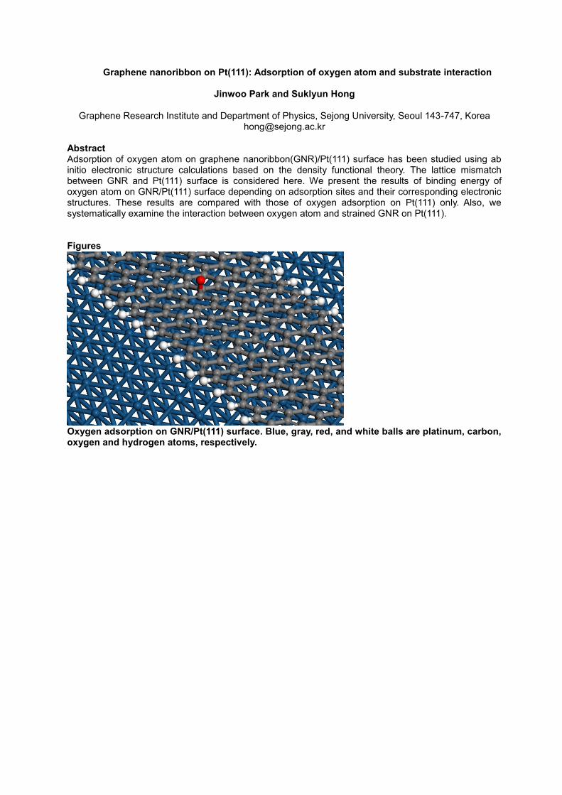
Graphene nanoribbon on Pt(111): Adsorption of oxygen atom and substrate interaction
Jinwoo Park and Suklyun Hong
Graphene Research Institute and Department of Physics, Sejong University, Seoul 143-747, Korea [email protected]
Abstract Adsorption of oxygen atom on graphene nanoribbon(GNR)/Pt(111) surface has been studied using ab initio electronic structure calculations based on the density functional theory. The lattice mismatch between GNR and Pt(111) surface is considered here. We present the results of binding energy of oxygen atom on GNR/Pt(111) surface depending on adsorption sites and their corresponding electronic structures. These results are compared with those of oxygen adsorption on Pt(111) only. Also, we systematically examine the interaction between oxygen atom and strained GNR on Pt(111). Figures
Oxygen adsorption on GNR/Pt(111) surface. Blue, gray, red, and white balls are platinum, carbon, oxygen and hydrogen atoms, respectively.
Nonlinear Optical response of graphene under CW He-Ne laser excitation
Poornesh P*, Pramodini S
Nonlinear Optics Research Laboratory, Department of Physics, Manipal Institute of Technology, Manipal University, Manipal, Karnataka, India-576 104
Abstract Rapid advances in the field of nanoscience and nanotechnology have enhanced the new opportunities for nonlinear optics. Large number of nanomaterials possessing noticeable nonlinear optical (NLO) properties has been investigated for optoelectronic and photonic device applications. Among the wide variety of materials investigated for nonlinear optical applications, graphene has drawn considerable interest due to its good optical transparency, robustness and environmental stability. Graphene is an one-atom-thick two-dimensional (2D) layers of carbon with a hexagonal packed structure [1]. Graphene being a carbon-based material offers flexibility in tailoring the NLO properties by modifying the chemical structure. In this article, we present nonlinear optical and optical limiting properties of graphene investigated using single beam Z-scan technique [2]. The experimental set up used is similar to that reported in the literature [3]. Experiments were performed by using Thor labs HRP350-EC-1 continuous wave (CW) He-Ne laser at 633nm wavelength as an excitation source and the resultant output power through the samples were recorded using a photo-detector fed to Thor labs PM320E dual channel optical power and energy meter. The laser beam with input power 21.9 mW was focused to a spot size of 36.78 µm and the Rayleigh length ZR of 6.71 mm using a 5 cm focal length lens. The thin sample approximation is valid, since the sample was taken in a quartz cuvette having an optical path of 1mm. The nonlinear absorption co-efficient eff , was measured using the Z-scan technique and found to be 1.21 x 10
-2 cm/W. Two photon absorption (TPA) found to be the nonlinear absorption process in
graphene. The UV-Vis absorption spectrum of the graphene shown in Figure1 reveals that there is strong absorption in the region 200nm to 350 nm, followed by a monotonously decrease in absorption towards long wavelength region. Optical limiting materials with low thresholds can be used for protection of eyes and sensitive optical devices from laser-induced damage. In this context, optical power limiting studies were carried out by placing the sample at the focal plane of the lens in the z-scan experiment. The input power of the laser beam was varied by using neutral density filter and the change in the output power was recorded using a photo-detector fed to power meter. The graphene exhibits a good optical power limiting behaviour under CW laser illumination at 633nm wavelength. Figure2 shows the optical power limiting behaviour of the graphene as a function of incident power varying from 0.2 mW to 20 mW. The optical limiting threshold for the graphene was found be ~4.5mW and the optical clamping occurs at ~3.4mW. The good optical power handling capability of laser beam at the 633nm experimental wavelength indicates the possible photonics device application of graphene such as all-optical power limiting. References [1] Geim AK, Novoselov KS. Nat Mater. 6 (2007)183.
[2] Pramodini S, Poornesh P and Nagaraja K K 13 (2013) Cur. Appl. Phys. 1175.
[3] Sheik-Bahae M, Said A A, Wei T H,Hagan D J, Van Stryland EW 26 (1990) IEEE. J. Quantum
Elect.760

Figures
Figure1. UV-Visible absorbance spectra of Graphene.
Figure2. Optical power limiting response of graphene under continuous wave 633nm irradiation.
P-doped CVD graphene on Si/SiO2 substrate
Nikos Delikoukos
1, Labrini Sygellou
1 ,Dimitrios Tasis
1, John Parthenios
1, Costas Galiotis
1,2 and
Konstantinos Papagelis1,2
1Foundation of Research and Technology Hellas, Institute of Chemical Engineering Sciences, P.O. Box
1414, GR-26504 Patras (Greece) 2Department of Materials Science, University of Patras, GR-26504 Patras (Greece)
Abstract Graphene has received much interest due the combination of extremely high mobility of carriers up to 2.5x10
5 cm
2V
-1s
-1
ideal candidate component in opto-electronic devices. To achieve complete graphene-based electronic circuits, optimization of transfer process to substrates and manipulation of carrier density are prerequisites and of great technological importance. On the other hand, the doping process, which involves controlling charge carrier type and concentration, is a reliable approach to tailor electronic properties of traditional semiconductor materials. Therefore, doping is an indispensible way to intentionally modulate the graphene electron/hole transport properties. In contrast to traditional semiconductors, the two-dimensional structure of graphene confines the doping process to surface adsorption. Dyes, polymers as well as fused aromatic systems have been used to realize either n-type or p-type doping in the liquid phase [1, 2]. Unfortunately, these reactive molecules may introduce parallel doping effects, due to utilization of liquid media for the doping step. Alternatively, doping can be achieved by means of gas-phase charge transfer in which the secondary doping effects are minimized. Elements such as alkali metals, and halogens show an efficient charge transfer doping effect. Yet, in most cases, they acquire high vacuum conditions for the production of vapors. Apart from these choices, charge transfer doping by gases or volatile liquids has attracted a lot of interest due to their easy control. A variety of substances possess good thermal stability and have very good volatility. Incorporated with the undisturbed basal plane electron conjugation, gas-phase molecular charge transfer doping provides a facile and effective method to dope graphene for future nanoelectronic applications. Recently, numerous reports have appeared in line with this route [3]. In this work, we present the gradual p-type surface doping of chemical vapor deposition (CVD) graphene transferred onto Si/SiO2 wafers. In this approach, HNO3 molecules are thermally deposited to form self-assembled charge transfer complexes. The charge transfer mechanism is experimentally interrogated by Raman, X-ray photoelectron (XPS) and Ultraviolet photoemission spectroscopy (UPS) for each doping step. Raman spectroscopy, owing to its sensitivity on the structural and electronic characteristics of graphene, has been proven to be a valuable non-destructive tool to detect, among the others, the doping state of graphene by probing the changes of the so-called G and 2D Raman active bands [4]. The UPS spectra were obtained using HeI irradiation with h = 21.23 eV produced by a UV source (model UVS 10/35). The work function ( ) was determined from the UPS spectra by subtracting their width (i.e. the energy difference between the analyzer Fermi level and the high binding energy
sample in order to avoid interference of the spectrometer threshold in the UPS spectra. In figure 1(left panel) the frequency position and the full width at half maximum (FWHM) of the G
band for untreated and doped graphene is presented. As can be clearly inferred from the figure the G band characteristics are position dependent. More specifically, in the pristine sample the mean value of the G peak position (FWHM) appears at 1589.2 cm
-1 (14.4 cm
-1) with a standard deviation of ±1.7cm
-1
(±2.1 cm-1
). After one hour of chemical treatment a significant shift of the mean G-mode frequency takes place occurring at 1593.8±1.6 cm
-1. Also, similar trend follows the FWHM(G) (11.5±1.5 cm
-1). For two
hours of chemical treatment the mean G-mode frequency (FWHM) reaches a value of 1598.7±2.5 cm-1
(10.2±2.8 cm
-1).Therefore, the adopted functionalization protocol cause solely charge transfer between
graphene and the adsorbed HNO3 molecules thus modifying the charge density in graphene membrane. The observed hardening of the G-band can be attributed to the shift of the Fermi energy level away from the Dirac points. The work function of undoped transferred graphene and after 2 doping steps was investigated using ultraviolet photoelectron spectroscopy (figure 1 right panel). As shown in the figure after doping the work function increases indicating that the Fermi level shifts closer to the valence band. It should be stressed that at each doping level after the UPS/XPS measurements a red shift of the collected Raman bands towards the corresponding untreated values is observed. This is attributed to
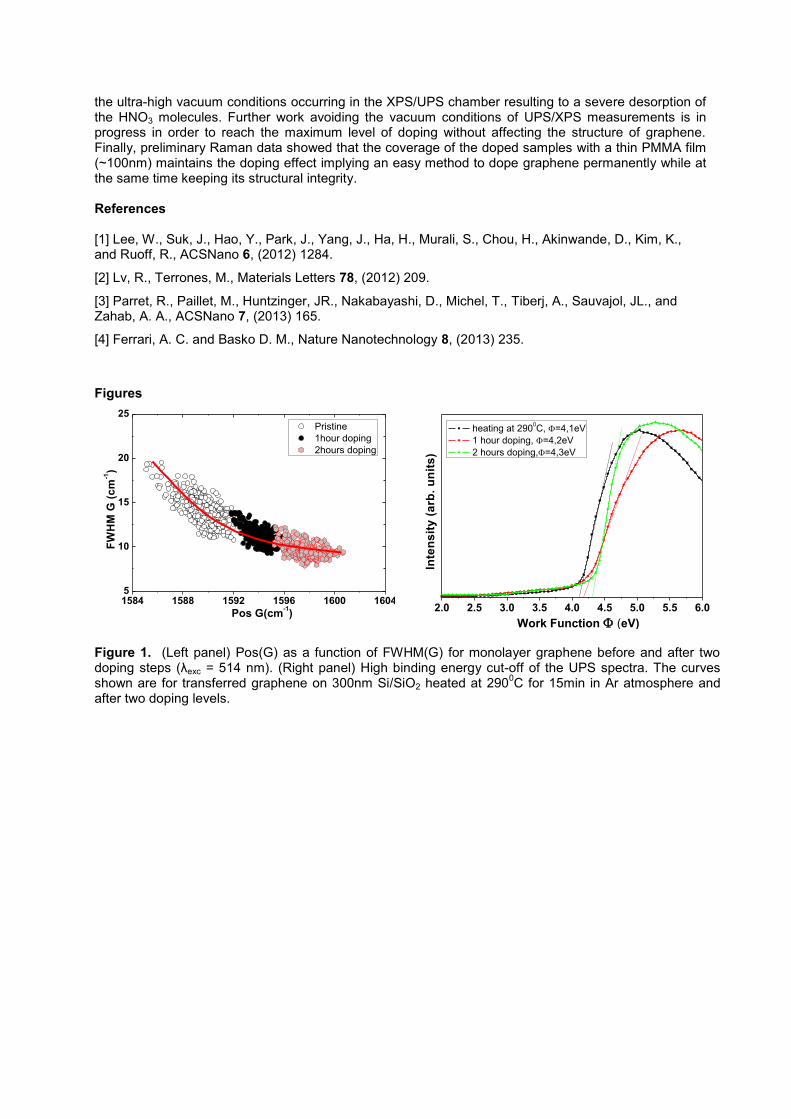
the ultra-high vacuum conditions occurring in the XPS/UPS chamber resulting to a severe desorption of the HNO3 molecules. Further work avoiding the vacuum conditions of UPS/XPS measurements is in progress in order to reach the maximum level of doping without affecting the structure of graphene. Finally, preliminary Raman data showed that the coverage of the doped samples with a thin PMMA film (~100nm) maintains the doping effect implying an easy method to dope graphene permanently while at the same time keeping its structural integrity.
References [1] Lee, W., Suk, J., Hao, Y., Park, J., Yang, J., Ha, H., Murali, S., Chou, H., Akinwande, D., Kim, K., and Ruoff, R., ACSNano 6, (2012) 1284.
[2] Lv, R., Terrones, M., Materials Letters 78, (2012) 209.
[3] Parret, R., Paillet, M., Huntzinger, JR., Nakabayashi, D., Michel, T., Tiberj, A., Sauvajol, JL., and Zahab, A. A., ACSNano 7, (2013) 165.
[4] Ferrari, A. C. and Basko D. M., Nature Nanotechnology 8, (2013) 235.
Figures
1584 1588 1592 1596 1600 16045
10
15
20
25
Pos G(cm-1)
FW
HM
G (
cm
-1)
Pristine
1hour doping
2hours doping
2.0 2.5 3.0 3.5 4.0 4.5 5.0 5.5 6.0
In
ten
sit
y (
arb
. u
nit
s)
Work Function (eV)
heating at 2900C, =4,1eV
1 hour doping, =4,2eV
2 hours doping, =4,3eV
Figure 1. (Left panel) Pos(G) as a function of FWHM(G) for monolayer graphene before and after two doping exc = 514 nm). (Right panel) High binding energy cut-off of the UPS spectra. The curves shown are for transferred graphene on 300nm Si/SiO2 heated at 290
0C for 15min in Ar atmosphere and
after two doping levels.

Electrostatics and drain current model of bilayer graphene field-effect transistors
Francisco Pasadas
*, David Jiménez
Departament d’Enginyeria Electrònica, Escola d’Enginyeria, Universitat Autònoma de Barcelona, Campus UAB, 08193 Bellaterra, Spain.
Abstract As predicted by Moore, the semiconductor industry has been facing an exponential growth of the number of transistors per chip during the last three decades. It is also predicted by ITRS (International Technology Roadmap for Semiconductors) that the gate length would scale down to 4.5 nm by 2023 [1]. However, maintaining this trend is a major challenge for both the industry and scientific community due to arising short channel effects. As a result, new device structures including FinFETs, nanowire FETs, and recently carbon nanotube field-effect transistors (CNTFETs) and graphene nanoribbon FETs have been proposed. Among them graphene based devices (either single layer graphene or bilayer graphene) have attracted the attention of scientific community due to the multitude of fascinating properties and the prospect of ultrahigh carrier mobilities exceeding those of the conventional semiconductors. This has motivated intensive work focused on the development of graphene metal-oxide-semiconductor field-effect transistors [2] (Figure 1). On the other hand, the gapless nature of single layer graphene, which is considered as the main obstacle on its application in graphene based electronics, causes the gate voltage to lose its control on switching off the device and are not suited for logic applications. However, it seems very promising for RF and analog applications because of the high transconductance and relatively low output conductance. Cut-off frequencies up to 427 GHz and maximum frequency of oscillation of 45 GHz has been demonstrated [3], which are important figure of merits in RF. Besides the metal-graphene contact resistance issue that strongly contribute to degrade the RF performances, the lack of a gap is also a detrimental factor preventing a full saturation of the drain current. However it has been recently demonstrated that bilayer graphene might come to rescue [4-6]. In bilayer graphene, a band gap is induced either by molecular doping or by applying a potential difference between two layers as a result of an external perpendicular electric field [7-9]. Moreover, the potential difference can be realized with an applied gate field which means the band gap can be controlled by gate bias [10-11] (Figure 2). In this work we have derived an analytical model for bilayer graphene field-effect transistors that properly accounts for the relevant physics. These kind of models are extremely useful to interpret experiments, guiding device design and exploring ultimate performances. Besides, they are key pieces of graphene-based circuit simulators, which are needed to design any circuit or calculate its figures of merit. Using this model we have demonstrated the superior saturation behavior (Figure 3) and the enhancement of the on/off current ratio (Figure 4) as compared with monolayer graphene. The physical framework applied has been a tight binding model of bilayer graphene [12-13], a field-effect model and drift-diffusion carrier transport [14-15]. References [1] International technology roadmap for semiconductors. http://www.itrs.net/. [2] Wu Y, Jenkins KA, Valdes-García A, Farmer DB, Zhu Y, Bol AA, Dimitrakopoulos C, Zhu W, Xia F,
Avouris P, Lin YM. Nano Lett. 12 (2012) 3062. [3] Schwierz F. Proceedings of the IEEE 101(7) (2013) 1567. [4] Fiori G, Neumaier D, Szafranek B, Iannaccone G. IEEE Trans. Elect. Dev. 61(3) (2014) 729. [5] Xia F, Farmer DB, Lin YM, Avouris P. Nano Lett. 10 (2010) 715. [6] Szafranek BN, Fiori G, Schall D, Neumaier D, Kurz H. Nano Lett. 12 (2012) 1324. [7] Yu WJ, Liao L, Chae SH, Lee YH, Duan X. Nano Lett. 11 (2011) 4759. [8] Samuels AJ, Carey JD. ACS Nano. 7(3) (2013) 2790. [9] Zhang W, Lin CT, Liu KK, Tite T, Su CY, Chang CH, Lee YH, Chu CW, Wei KH, Kuo JL. ACS
Nano 5 (2011) 7517. [10] Castro EV, Novoselov KS, Morozov SV, Peres NMR, Lopes dos Santos JMB, Nilsson J, Guinea F,
Geim AK, Castro Neto AH. Phys. Rev. Lett. 99 (2007) 216802. [11] Zhang Y, Tang TT, Girit T, Hao Z, Martin MC, Zettl A, Crommie MF, Shen YR, Wang F. Nature
Lett. 459 (2009) 820. [12] McCann E, Koshino M. Rep. Prog. Phys. 76 (2013) 056503.

[13] Cheli M, Fiori G, Iannaconne G. IEEE Trans. Elect. Dev. 56(12) (2009) 2979. [14] Jiménez D. IEEE Trans. Elect. Dev. 58 (2011) 4377. [15] Thiele SA, Schaefer JA, Schwierz F. Journal of Applied Physics 107 (2010) 094505. Figures
Figure 1 Cross section of the bilayer graphene field effect transistor. Here, and are the top and back oxide
thicknesses, and are the top and back dielectric relative permittivities, and are the top and back gate
voltages and is the drain-to-source voltage.
Figure 3 Output characteristics of a double gate bilayer graphene field effect transistor ( = 300 , = 10 ,
= 3.9, = 3.2).
Figure 2 Energy band diagram of a double gate bilayer
graphene field effect transistor ( = 300 , = 10 ,
= 3.9, = 3.2).
Figure 4 Transfer characteristics of a double gate bilayer graphene field effect transistor ( = 300 , = 10 ,
= 3.9, = 3.2).

Graphene growth on bronze substrates
I. Pasternak1, R. Jakiela
1,2, G. Gawlik
1, W. Strupinski
1
1 Institute of Electronic Materials Technology, Wolczynska 133, 01-919 Warsaw, Poland
2 Institute of Physics Polish Academy of Sciences, Al. Lotnikow 32/46, 02-668 Warsaw, Poland
To take full advantage of the properties of graphene, including extraordinary resistance to
environmental factors or mechanical strength, its use in the bronze elements of a servomechanism
has been considered. Bronzes belong to the category of copper-based substrates characterized by
good antifriction properties and high resistance to heat-treatment and corrosion. Nevertheless,
coupling graphene and bronze substrates together is expected to enhanced their features even more.
In the present work, we have fabricated graphene on a silicon bronze surface. Typically, the
content of silicon in such copper-based substrates varies from 0.01% to 3.5%. Moreover, we have
provided results obtained for a graphene coating formed on tin bronzes. The manufacturing process of
graphene has been performed under carefully arranged conditions, taking into account the physical
properties of silicon bronze. To obtain graphene of top quality we have used an Aixtron VP508
horizontal CVD hot wall reactor and propane gas as a carbon precursor.
Our investigations have shown that with increasing the content of silicon in copper-based
substrates, the quality of the obtained graphene films decreases [Fig. 1]. To support the
abovementioned conclusion, we have collated SIMS depth profiles for Cu:Si alloys and Raman
spectra taken from the surfaces of Cu:Si alloys after graphene deposition. Additionally, we have
presented findings for tin bronzes on top of which we have obtained monolayer graphene films.
Figures:
1400 1600 1800 2000 2200 2400 2600 2800
Inte
nsity [a
.u]
Raman shift [cm-1]
0.01% Si
0.1% Si
1% Si
Figure 1. Raman spectra of graphene on copper-based substrates with a differ content of
silicon.
Acknowledgments: This work was partially supported by the the National Centre for Research and Development by project no GRAF-TECH/NCBR/05/12/2012.
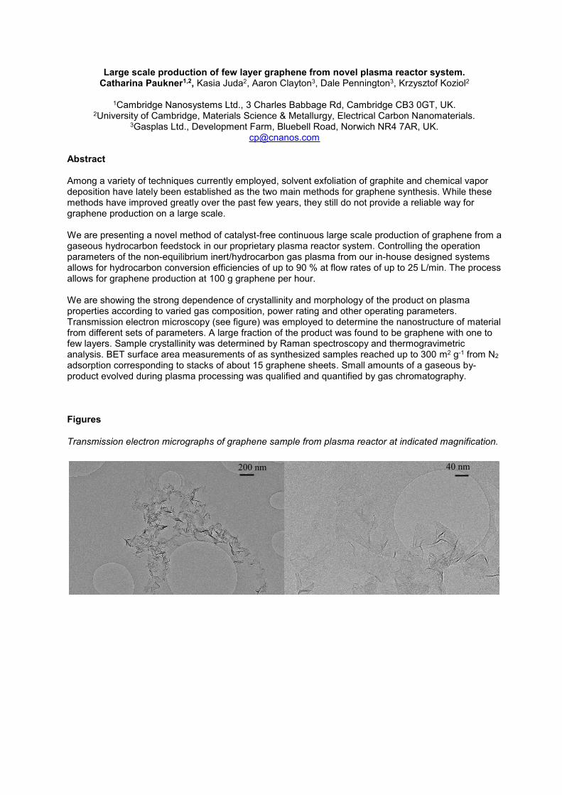
Large scale production of few layer graphene from novel plasma reactor system. Catharina Paukner1,2, Kasia Juda2, Aaron Clayton3, Dale Pennington3, Krzysztof Koziol2
1Cambridge Nanosystems Ltd., 3 Charles Babbage Rd, Cambridge CB3 0GT, UK.
2University of Cambridge, Materials Science & Metallurgy, Electrical Carbon Nanomaterials. 3Gasplas Ltd., Development Farm, Bluebell Road, Norwich NR4 7AR, UK.
Abstract Among a variety of techniques currently employed, solvent exfoliation of graphite and chemical vapor deposition have lately been established as the two main methods for graphene synthesis. While these methods have improved greatly over the past few years, they still do not provide a reliable way for graphene production on a large scale. We are presenting a novel method of catalyst-free continuous large scale production of graphene from a gaseous hydrocarbon feedstock in our proprietary plasma reactor system. Controlling the operation parameters of the non-equilibrium inert/hydrocarbon gas plasma from our in-house designed systems allows for hydrocarbon conversion efficiencies of up to 90 % at flow rates of up to 25 L/min. The process allows for graphene production at 100 g graphene per hour. We are showing the strong dependence of crystallinity and morphology of the product on plasma properties according to varied gas composition, power rating and other operating parameters. Transmission electron microscopy (see figure) was employed to determine the nanostructure of material from different sets of parameters. A large fraction of the product was found to be graphene with one to few layers. Sample crystallinity was determined by Raman spectroscopy and thermogravimetric analysis. BET surface area measurements of as synthesized samples reached up to 300 m2 g-1 from N2 adsorption corresponding to stacks of about 15 graphene sheets. Small amounts of a gaseous by-product evolved during plasma processing was qualified and quantified by gas chromatography. Figures
Transmission electron micrographs of graphene sample from plasma reactor at indicated magnification.
200 nm 40 nm
Characterization of graphene synthesized by electrolysis in aqueous electrolytes
Aleksandar Petrovski, Aleksandar T. Dimitrov, Anita Grozdanov, Beti Andonovic and
Electrochemical approach is a suitable alternative for a high-yield production of graphene. Electrolysis in aqueous electrolytes is simple, environmentally friendly, economic, as it occurs under ambient conditions, and flexible process, due to the thickness control by potential or current adjustment, providing synthesis of high quality graphene. The studied graphene material was produced by electrolysis in acid aqueous electrolysis using reverse change of the applied voltage. Highly oriented graphite was used as electrodes (precursors for graphene production). Three types of electrolytes were used: H2SO4 (pH = 0.5), H2SO4 + KOH (pH = 1.2), and H2SO4 + NaOH (pH = 1.2). Characterization of the synthesized graphene was performed by means of scanning and transmission electron microscopy (SEM and TEM), infrared spectroscopy (FTIR), thermal analysis (TG, DTA and DTG), Raman spectroscopy and X-ray diffraction (XRD). Determination of crystallite size and number of graphene layers was done using Raman and XRD spectra. It was found that the dominant structure is few-layered graphene, with an average value for number of graphene layers calculated as n = 3.53, whereas the number of graphene layers for the overall graphene structure was calculated as n = 5.6.
Key words: graphene, electrolysis, aqueous electrolyte, layers, crystallite size.
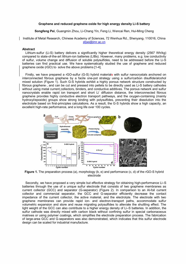
Graphene and reduced graphene oxide for high energy density Li-S battery
Songfeng Pei, Guangmin Zhou, Li-Chang Yin, Feng Li, Wencai Ren, Hui-Ming Cheng
Institute of Metal Research, Chinese Academy of Sciences, 72 Wenhua Rd., Shenyang, 110016, China [email protected]
Abstract
Lithium-sulfur (Li-S) battery delivers a significantly higher theoretical energy density (2567 Wh/kg) compared to state-of-the-art lithium-ion batteries (LIBs). However, many problems, e.g. low conductivity of sulfur, volume change and diffusion of soluble polysulfides, need to be addressed before the Li-S batteries can find practical use. We have systematically studied the use of graphene and reduced graphene oxide (rGO) to solve the above problems [1-4].
Firstly, we have prepared a rGO-sulfur (G-S) hybrid materials with sulfur nanocrystals anchored on interconnected fibrous graphene by a facile one-pot strategy using a sulfur/carbon disulfide/alcohol mixed solution (Figure 1). Such G-S hybrids exhibit a highly porous network structure constructed by fibrous graphene , and can be cut and pressed into pellets to be directly used as Li-S battery cathodes without using metal current collectors, binders, and conductive additives. The porous network and sulfur nanocrystals enable rapid ion transport and short Li
- diffusion distance, the interconnected fibrous
graphene provides highly conductive electron transport pathways, and the oxygen-containing (mainly hydroxyl/epoxide) groups show strong binding with polysulfides, preventing their dissolution into the electrolyte based on first-principles calculations. As a result, the G-S hybrids show a high capacity, an excellent high-rate performance, and a long life over 100 cycles.
Figure 1. The preparation process (a), morphology (b, e) and performance (c, d) of the rGO-S hybrid
electrode
Secondly, we have proposed a very simple but effective strategy for obtaining high-performance Li S batteries through the use of a unique sulfur electrode that consists of two graphene membranes as current collector (GCC) and separator (G-separator) (Figure 2). In comparison to an Al-foil current collector and commercial separator, the GCC and G-separator efficiently decrease the contact impedance of the current collector, the active material, and the electrolyte. The electrode with two graphene membranes can provide rapid ion- and electron-transport paths, accommodate sulfur volumetric expansion and store and reuse migrating polysulfides to alleviate the shuttling effect. The light weight of the GCC can also contribute to a higher energy density of Li S batteries. In addition, the sulfur cathode was directly mixed with carbon black without confining sulfur in special carbonaceous matrixes or using polymer coatings, which simplifies the electrode preparation process. The fabrication of large-area GCC and G-separators was also demonstrated, which indicates that this sulfur electrode design can be scaled for industrial manufacture.
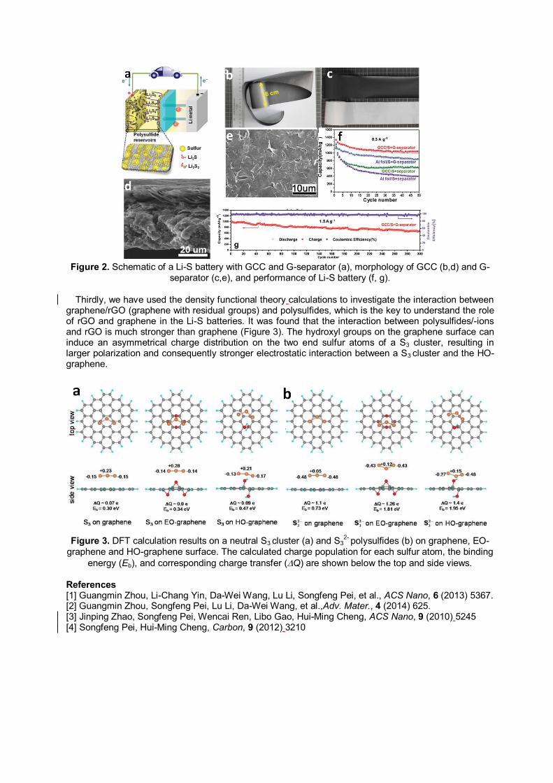
Figure 2. Schematic of a Li-S battery with GCC and G-separator (a), morphology of GCC (b,d) and G-
separator (c,e), and performance of Li-S battery (f, g).
Thirdly, we have used the density functional theory calculations to investigate the interaction between graphene/rGO (graphene with residual groups) and polysulfides, which is the key to understand the role of rGO and graphene in the Li-S batteries. It was found that the interaction between polysulfides/-ions and rGO is much stronger than graphene (Figure 3). The hydroxyl groups on the graphene surface can induce an asymmetrical charge distribution on the two end sulfur atoms of a S3 cluster, resulting in larger polarization and consequently stronger electrostatic interaction between a S3 cluster and the HO-graphene.
Figure 3. DFT calculation results on a neutral S3 cluster (a) and S3
2- polysulfides (b) on graphene, EO-
graphene and HO-graphene surface. The calculated charge population for each sulfur atom, the binding
energy (Eb), and corresponding charge transfer ( Q) are shown below the top and side views.
References [1] Guangmin Zhou, Li-Chang Yin, Da-Wei Wang, Lu Li, Songfeng Pei, et al., ACS Nano, 6 (2013) 5367. [2] Guangmin Zhou, Songfeng Pei, Lu Li, Da-Wei Wang, et al.,Adv. Mater., 4 (2014) 625. [3] Jinping Zhao, Songfeng Pei, Wencai Ren, Libo Gao, Hui-Ming Cheng, ACS Nano, 9 (2010) 5245 [4] Songfeng Pei, Hui-Ming Cheng, Carbon, 9 (2012) 3210

Contribution (Poster)
Functionalization of RGO sheets with Polysulfone brushes to design nanocomposites
Peña-Bahamonde J.,San Miguel V., Baselga J., Cabanelas J.C.
Universidad Carlos III de Madrid. Avda. De la Universidad, 30. 28911, Leganes (Madrid) Spain. [email protected]
Polysulfones (PSUs) are high-temperature thermoplastic polymers that exhibit great chemical inertness, enhanced oxidative resistence, thermal and hydrolytic stability, as well as high mechanical strength. Additionally, PSUs might be easily processed as a film and thus, they are good candidates for different applications, such as gas separation, hemodialysis, nano/ultra-filtration, adhesives for metal to metal bonds, membranes for fuel cells, drug delivery, or matrices for fiber reinforced composites.
1,2
Polymer-matrix nanocomposites formed by incorporation of graphene sheets in polymer matrices have attracted enormous attention in various fields of science and engineering, due to the excellent properties of graphene sheets. In recent years, graphene-based polymer nanocomposites have been used to improve the mechanical, thermal, electrical and gas barrier properties of polymers and have shown great potential for diverse applications in electronics, aerospace, automotive manufacturing and green energy.
3,4,5
In this work, we report a comparative study of the mechanical and electrical properties of different nanocomposites based on reduced graphene oxide sheets (RGO) covalently modified with PSU or without surface modification, in every case dispersed in a PSU matrix. GO was synthesized using Brodie method
6 and then thermally reduced under a hydrogen atmosphere.
RGO surface was modified by two different chemical routes7,8
(Figure 1) to improve its interfacial compatibility with the PSU matrix. Both synthesis methods allowed anchoring polymer chains to RGO sheets. By controlling the anchor point of the PSU to the RGO (Route 1 or 2, Figure 1) it was possible to obtain composites wherein the polymer was bonded at the end or in the middle of the chain (RGO-PSU-ext and RGO-PSU-mid, respectively).
The resulting RGO-PSU nanocomposites were carefully characterized by raman spectroscopy, infrared spectroscopy, differential scanning calorimetry, thermogravimetric analysis, and nuclear magnetic resonance, evidencing the successful anchoring of polymer onto the surface of RGO (Table 1). Furthermore, the modified RGO dispersions exhibit long-term stability in common solvents.
PSU nanocomposites were prepared with different percentages of PSU-RGO (up to 1%) by extrusion. The extruded material was further processed by injection molding to finally obtain specimens for mechanical and electrical tests.
The morphology and microstructure of the prepared samples were examined with a scanning electron microscopy (SEM). The mechanical strength was evaluated using a Shimadzu Autograph testing machine with a 1KN load cell. Furthermore, samples were analyzed by dynamic mechanical thermal analysis (DMTA) and differential scanning calorimetry (DSC), and the electrical conductivity was determined using a HP34401 device.
In this work, modified graphene with polysulfone was successfully obtained by nitrene chemistry. Moreover, the surface modification of RGO has ended up being a great strategy for enhancing its dispersion in the PSU matrix. The results indicate that the extrusion-injection procedure enables to efficiently prepare PSU-RGO nanocomposites with good dispersion degrees of RGO in the matrix. The enhancement of mechanical and electrical properties was interpreted in terms of the dispersion and interface modification of RGO.

Contribution (Poster)
References
[1] Mcgrail, P. T. Polym. Int. 41 (1996) 103-121.[2] Cemil, D. Mehmet A.T. & Yusuf,Y. Polym. Int. 62 (2013) 991-1007. [3] Sasha Stankovich, Dmitriy A. Dikin, Geoffrey H. B. Dommett, Kevin M. Kohlhaas, Eric J. Zimney, Eric A. Stach, Richard D. Piner, SonBinh T. Nguyen & Rodney S. Ruoff . Nature 442 (2006) 282–286. [4] Du, J. & Cheng, H. Macromol. Chem. Phys. 213 (2012) 1060–1077.[5] Tapas K, Sambhu B, Dahu Y, Nam H. K, Saswata B, Joong H. Lee. Prog. Polym. Sci. 35 (2010) 1350–1375. [6] Brodie B.C, Philos. Trans. R. Soc. London 149 (1859) 249–259. [7] Toiserkani, H., Yilmaz, G., Yagci, Y. & Torun, L. Macromol. Chem. Phys. 211 (2010) 2389– 2395. [8] He, H. & Gao, C.Chem. Mater. 22 (2010) 5054–5064.
Sample
TGA Raman
Weight loss (%)
Polymer chains per 1000 carbon
atoms
Polymer chains
per µm-2
(·10-4
)
Raman shift (cm
-1) ID/IG
ID IG
RGO 18.3 -- -- 1367 1594 0.802
RGO-PSU ext 32.0 1.3 2.5 1381 1580 0.629
RGO-PSU mid 29.1 1.2 2.3 1375 1589 0.740
������
��������������
���������������
��������� ����
�������
������������������� ��������� ��
���������������
��������� ����
�� ���������� ��������
������������
�
��
�
� � �
� �
Figure 1: Scheme of the different grafted PSU onto the RGO surface
Table 1: Characterization of modified RGO by TGA and Raman Spectroscopy

Effective contact model for geometry-independent conductance calculations in
graphene
D. A. Bahamon1,2
, A. H. Castro Neto2
and Vitor M. Pereira2
1MackGraphe – Graphene and Nano-Materials Research Center. Mackenzie Presbyterian University.
Rua da Consolação, 900 – São Paulo, Brazil.2Graphene Research Centre and Department of Physics, National University of Singapore, Singapore
117542, Singapore
Abstract The starting point of any calculation of quantum conductance in the Landauer-Büttiker formalism using Green’s functions (GF) is Caroli’s formula. This formula has been extensively used for nanoribbons geometries, but the only restriction about the geometry of the nanostructure is the GF of the contacts. As far as we know, this is the first attempt to adapt the GF’s method to a Corbino disk geometry. Our method assumes that the contact is an s band metal and that its DOS is nearly constant at the Fermi Energy; based on these an effective self-energy term is introduced in the GF’s calculation of the quantum conductance [1]. When compared with the results obtained by Dirac’s equation [2] our calculations agrees with the conductance obtained via the Dirac equation (GD) irrespective of the geometric parameters like inner radius (Ri) and outer radius (Ro), as can be seen in Fig. 1 where the normalized conductance is shown as a function of the Fermi energy in the annulus region forRi/Ro=0.007,0.86,0.47. This range of geometric parameters was chosen to analyze the effect of the disk size (number of atoms) on the conductance, and also to allow us to probe the effect of varying the number of edge atoms (atoms with on-site energy modified by the effective self-energy term).Surprisingly the conductance as a function of energy doesn’t show plateaus for the total angular momentum eigen-channels, being characterized only by Fabry-Perot oscillations that are more prominent in our model because of the roughness of the metal-graphene interface. For wide disks the conductance at the Dirac point is reduced but never reaches zero, as would be expected in a semi-classical calculation, due to the influence of evanescent states. Evanescent states are also responsible for higher values of conductance for larger inner radii, since more total angular momentum eigen-channels are allowed to transmit. Our model reproduces the magneto-conductance characteristics of a Corbino disk as well. The advantage of GF’s methods is the possibility of introducing disorder, which we explore and characterize by adding short-range onsite disorder (Anderson type) in order to calculate the radial part of the conductivity tensor (σrr).
References
[1] D. A. Bahamon, A. H. Castro Neto and Vitor M. Pereira, Phys. Rev. B, 88 (2013) 235433
[2] A. Rycerz, P. Recher and M. Wimmer, Phys. Rev. B, 80 (2009) 125417
Figures

Figure 1. Energy dependence of the conductance normalized by R_i for different values of Ri and Ro, calculated using Dirac eqution (labeled ``D'') and the lattice Green's function approach (labeled ``G''). The inset shows the relative differences in the values of conductance calculated by the two methods ∆G= 100(GD-GG)/GD.
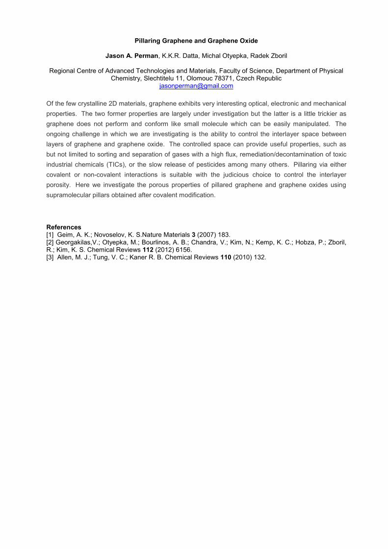
Pillaring Graphene and Graphene Oxide
Jason A. Perman, K.K.R. Datta, Michal Otyepka, Radek Zboril
Regional Centre of Advanced Technologies and Materials, Faculty of Science, Department of Physical
Chemistry, Slechtitelu 11, Olomouc 78371, Czech Republic [email protected]
Of the few crystalline 2D materials, graphene exhibits very interesting optical, electronic and mechanical
properties. The two former properties are largely under investigation but the latter is a little trickier as
graphene does not perform and conform like small molecule which can be easily manipulated. The
ongoing challenge in which we are investigating is the ability to control the interlayer space between
layers of graphene and graphene oxide. The controlled space can provide useful properties, such as
but not limited to sorting and separation of gases with a high flux, remediation/decontamination of toxic
industrial chemicals (TICs), or the slow release of pesticides among many others. Pillaring via either
covalent or non-covalent interactions is suitable with the judicious choice to control the interlayer
porosity. Here we investigate the porous properties of pillared graphene and graphene oxides using
supramolecular pillars obtained after covalent modification.
References [1] Geim, A. K.; Novoselov, K. S.Nature Materials 3 (2007) 183. [2] Georgakilas,V.; Otyepka, M.; Bourlinos, A. B.; Chandra, V.; Kim, N.; Kemp, K. C.; Hobza, P.; Zboril, R.; Kim, K. S. Chemical Reviews 112 (2012) 6156. [3] Allen, M. J.; Tung, V. C.; Kaner R. B. Chemical Reviews 110 (2010) 132.

Reconfigurable Gate-free Graphene Stacks at THz
J. Perruisseau-Carrier1, J. S. Gomez-Diaz
1, C. Moldovan
2, S. Capdevila
4, J. Romeu
4, L. S. Bernard
3,
A. Magrez3, and A. M. Ionescu
2
1Adaptive MicroNanoWave Systems Group, EPFL, 1015 Lausanne, Switzerland
2Nanolab, EPFL, 1015 Lausanne, Switzerland.
3ICMP, EPFL, 1015 Lausanne, Switzerland
4AntenaLAB, Universitat Politècnica de Catalunya, 08034 Barcelona, Spain
Abstract The unique electrical properties of graphene [1] has led to the development of a wide variety of reconfigurable plasmonic THz devices, including waveguides [2, 3], resonant [4, 5] and leaky-wave antennas [6, 7] or periodic metasurfaces [8]. From the experimental point of view, single-layer graphene structures have already been characterized in the microwave [9] and terahertz [10] frequency ranges, and some promising applications, such as Faraday rotators [11] and modulators [12], have been demonstrated. However, the simple implementation and performance of these devices might be hindered by two main factors: i) the presence of a gating structure closely located to graphene, and ii) restricted control on graphene conductivity. These limitations can be overcame by using graphene stacks [3, 4, 8, 12], structures composed of two or more isolated graphene layers separated by electrically thin dielectrics, which lead to low surface resistances and may provide novel reconfiguration strategies. In the literature, this type of structures has been employed to investigate the Anderson localization of Dirac electrons at DC, which occurs in one of the graphene layers due to the “screening” effect provided by the other one [13, 14]. However, the potential of graphene stacks for THz plasmonics has not been fully considered yet.
In this context, we present here our first steps towards the experimental characterization of reconfigurable graphene stacks for THz plasmonics. Specifically, a single-layer graphene and a double-layer graphene stack have been fabricated using CVD graphene grown on Cu foil and transferred onto a substrate using the standard wet transfer method (see details in Fig. 1). In the case of the single-layer structure (Fig.1, left), the gate voltage is applied between graphene and a polysilicon layer located beneath the dielectric insulator. In contrast, in the case of the stack (Fig. 1, right), the gate voltage is applied between the two graphene layers which compose the structure thus allowing to the graphene sheets to bias each other. Note that more advanced reconfiguration strategies can easily be developed by including additional gate voltages to this structure. The samples are then measured in transmission using terahertz time-domain spectroscopy (TDS), and the conductivity of the single-layer graphene and stack structures are retrieved using a dedicated formulation. Fig. 2 shows the real part of the extracted conductivity versus the applied voltage for both structures at the operation frequency f=1.5 THz. Results clearly confirm the reconfiguration capabilities of the samples at terahertz, demonstrating the ability of the graphene stack to self-bias without requiring additional gating components. In addition, note that the extracted conductivities possess hysteresis depending on the gate sweeping features. This phenomenon arises due to the charges and impurities trapped in the dielectric, as occurs in graphene transistors [15], and can be significantly reduced by applying an annealing process.
The results shown here will be expanded at the conference by studying the frequency dependent behaviour of the extracted conductivity, by further investigating the reconfiguration capabilities of graphene stacks when various gate voltages are considered, and by proposing a simple theoretical model able to characterize the proposed structure. The experimental results shown here are very promising for the future integration of graphene in tunable plasmonic THz devices.
Acknowledgements This work was partially supported by the Swiss National Science Foundation (SNSF) under grant 133583, by the European Commission FP7 projects “Grafol” (Grant. No. 133583), Marie-Curie IEF “Marconi” (ref. 300966) and Marie-Curie ITN “NAMASEN”.
References [1] K. Geim and K. S. Novoselov, Nature Materials, vol. 6 (2007), pp. 183–191. [2] J. Christensen, A. Manjavacas, S. Thongrattanasiri, F. H. L. Koppens, and F. J. G. de Abajo, ACS Nano, vol. 6 (2012), pp. 431–440. [3] D. Correas-Serrano, J. S. Gomez-Diaz, J. Perruisseau-Carrier, and A. Alvarez-Melcon, IEEE Transactions on Microwave Theory and Techniques, vol. 61 (2013), pp. 4333–4344.
[4] M. Tamagnone, J. S. Gomez-Diaz, J. R. Mosig, and J. Perruisseau-Carrier, Applied Physics Letters, vol. 101 (2012), p. 214102. [5] R. Filter, M. Farhat, M. Steglich, R. Alaee, C. Rockstuhl, and F. Lederer, Opt. Express, vol. 21(2013), pp. 3737-3745. [6] J. S. Gomez-Diaz, M. Esquius-Morote, and J. Perruisseau-Carrier, Optic Express, vol. 21 (2013), pp. 24 856–24 872. [7] M. Esquius-Morote, J. S. Gomez-Diaz, and J. Perruisseau-Carrier, IEEE Transactions on Terahertz Science and Technology, vol. 4 (2014), pp. 116–122. [8] A. Fallahi and J. Perruisseau-Carrier, Physical Review B, vol. 86 (2012), p. 195408. [9] J. S. Gomez-Diaz, J. Perruisseau-Carrier, P. Sarma, and A. Ionescu, Journal of Applied Physics, vol. 111 (2012), p. 114908. [10] L. Ren, Q. Zhang, J. Yao, Z. Sun, R. Kaneko, Z. Yan, S. Nanot, Z. Jin, I. K. amd M. Tonouchi, J. M. Tour, and J. Kono, Nano Letters, vol. 12 (2012), pp. 3711–3715. [11] I. Crassee, J. Levallois, A. L. Walter, M. Ostler, A. Bostwick, E. Rotenberg, T. Seyller, D. van der Marel, and A. B. Kuzmenko, Nature Physics, vol. 7 (2010), pp. 48–51. [12] B. Sensale-Rodriguez, R. Yan, M. M. Kelly, T. Fang, K. Tahy, W. S. Hwang, D. Jena, L. Liu, and H. G. Xing, Nature Communications, vol. 3 (2012), p. 780. [13] K. Kechedzhi, E. H. Hwang, and S. D. Sarma, Physical Review B, vol. 86 (2012), p. 165442. [14] R. V. Gorbachev, A. K. Geim, M. I. Katsnelson, K. S. Novoselov, T. Tudorovskiy, I. V. Grigorieva, A. H. MacDonald, S. V. Morozov, K. Watanabe, T. Taniguchi, and L. A. Ponomarenko, Nature Physics, vol. 85 (2012), p. 075410. [15] H. Wang, Y. Wu, C. Cong, J. Shang, and T. Yu, ACS Nano, vol. 4 (2010), pp. 7221–7228. [16] S. H. Lee, M. Choi, T. Kim, S. Lee, M. Lui, X. Yin, H. K. Choi, S. S. Lee, C. Choi, S. Choi, X. Zhang, and B. Min, Nature Materials, vol. 11 (2012), pp. 936–941.
Figures
Figure 1: Single graphene layer (left column) and double-layer graphene stack (right column) structures
considered in this work.
a) b)
Figure 2: Measured real part of the conductivity (real part) related to the single-layer graphene (a) and double-
layer (b) graphene structures shown in Fig. 1 versus the applied gate voltage at 1.5 THz. Results clearly confirm
the hysteresis behavior of graphene conductivity at terahertz. In the case of the single layer graphene, conductivity
is plotted before and after applying an annealing process to the sample.

Hall effect detection of optically invisible defects in CVD graphene
D.H. Petersen1, D. Kjær
2, M. Lotz
1, M. Boll
1, J.D. Buron
1, B.S. Jessen
1,
F. Pizzocchero1, P.F. Nielsen
2, P.U. Jepsen
3, P. Bøggild
1, O. Hansen
1
1DTU Nanotech, Building 345 East, DK-2800 Kgs. Lyngby, Denmark
2Capres A/S, Diplomvej, Building 373, DK-2800 Kgs. Lyngby, Denmark 3DTU Photonics, Building 345 West, DK-2800 Kgs. Lyngby, Denmark
Abstract The presence of transfer defects and grain boundaries in large area CVD graphene is a well-known problem in fabrication of reliable graphene based devices (1-4). While difficult to identify through optical methods, it was recently demonstrated that defects may be detected statistically via dual configuration four-point probe (4PP) resistance measurements (5). We now present a complementary method, based on a scanning Hall Effect method, in which a magnetic field is applied normal to the graphene film. On a 2D conductive film without defects, the 4PP resistance will change purely due to the Corbino Effect. However, a unique Hall signal appears when the Lorentz force induced current rotation is obstructed by defects. The Hall signal increases in amplitude when approaching an insulating boundary, and an abrupt sign change occurs when stepping across a boundary. This is demonstrated in fig. 1a where a 4PP is scanned across macroscopic defects, some of which are not even visible with high resolution optical microscopy, cf. fig. 1a (top). In Fig. 1a, large Hall signals coincide with a drop in the measured sheet conductance (GS). This correlation is emphasized in the correlation plot, fig. 1c. Here, it is important to realize that whereas reduced sheet conductance could result from spatial doping variations in graphene, the Hall effect signal only appears in the presence of defects. We use the new Hall effect detection method to study defects in graphene at different length scales using 4PPs with pitch ranging from 4 µm to 100 µm. By conformal mapping, cf. fig. 2, we then evaluate analytically the sensitivity of the Hall method to linear defect perturbations of different sizes, rotation and position. References [1] Y. Lee, S. Bae, H. Jang, S. Jang, S.-E. Zhu, S.H. Sim, Y.I. Song, B.H. Hong, J.-H. Ahn, Nano Lett.
10 (2010) 490-493. [2] P.Y. Huang, C.S. Ruiz-Vargas, A.M. van der Zande, W.S. Whitney, M.P. Levendorf, J.W. Kevek, S.
Garg, J.S. Alden, C.J. Hustedt, Y. Zhu, J. Park, P.L. McEuen, D.A. Muller, Nature 469 (2011) 389-392.
[3] Q. Yu, L.A. Jauregui, W. Wu, R. Colby, J. Tian, Z. Su, H. Cao, Z. Liu, D. Pandey, D. Wei, T.F.
Chung, P. Peng, N.P. Guisinger, E.A. Stach, J. Bao, S.-S. Pei, Y.P. Chen, Nature Materials 10 (2011) 443-449.
[4] Dae Woo Kim, Yun Ho Kim, Hyeon Su Jeong, Hee-Tae Jung, Nature Nanotechnology 7 (2012) 29
34. [5] J.D. Buron, D.H. Petersen, P. Bøggild, D.G. Cooke, M. Hilke, J. Sun, E. Whiteway, P.F. Nielsen, O.
Hansen, A. Yurgens, P.U. Jepsen, Nano Lett. 12 (2012) 5074-5081.

Figures
Fig. 1: Hall effect line scan on single layer CVD graphene. (a) Hall effect and sheet conductance line scan along the area depicted in the contrast enhanced stitched optical micrograph (top). (b) Illustration of Hall effect measurement on graphene film with defects. (c) Correlation plot showing the relationship between the measured sheet conductance and Hall signal.
Fig. 2: Conformal mapping of a line defect to the upper half plane geometry that may be solved analytically for any positions of the defect and electrodes.

Step-wise reduction of immobilized monolayer graphene oxides
Søren Vermehren Petersen,
1 Yudong He,
2Jiang Lang,
2 Filippo Pizzocchero,
3 Nicolas Bovet,
1 Peter
Bøggild,3 Wenping Hu,
2 and Bo W. Laursen
1
1 Nano-Science Center & Department of Chemistry, University of Copenhagen, Copenhagen, Denmark
2 Institute of Chemistry, Chinese Academy of Science, Beijing, China
3 DTU Nanotech, Technical University of Denmark, Lyngby, Denmark
Abstract Chemically converted graphene is highly relevant for transparent conducting film applications such as display and photovoltaic applications [1]. So far, the major obstacle for realizing the potential has been to fully reduce/deoxygenate the graphene oxide (GO), which is challenging in part due to the pronounced aggregation that accompanies deoxygenation of GO in solution [2]. Surface immobilization of monolayered graphene oxide (mGO) in Langmuir-Blodgett (LB) films was investigated as a method to circumvent this problem [3]. Two types of LB films with different density of mGO flakes where prepared, i.e. diluted and coherent, and efficiently deoxygenated in a three-step reduction procedure involving subsequent treatment with hydrazine in dimethylformamide (DMF) to give rGO1, sulfuric acid to give rGO2, and high temperature annealing to give rGO3. The stepwise reduction process was evaluated with optical microscopy, Raman microscopy, and X-ray photoelectron spectroscopy (XPS) along with electrical characterization. XPS measurements confirmed a full conversion into virtually oxygen free chemically converted graphene. The electrical characterization revealed large variations in the conductivity for single sheets in the diluted LB films, with an average conductivity of 100 S/cm. A similar conductivity was found for macroscopic devices made from the coherent LB films with overlapping mGO sheets. The large variation in single sheets conductance is assigned to over-oxidation of the GO leading to formation of holes, which cannot be recovered in the chemical reduction procedure. The study show that the applied three-step reduction procedure is chemically complete and that the conductivity of this chemically converted graphene is limited by structural defects/holes rather than remaining oxygen functionalities.
References [1] Yin, Z. et al., Acs Nano, 4 (2010), 5263-5268. [2] Stankovich, S. et al., Carbon, 45 (2007), 1558-1565. [3] Petersen, S. V. et al., Chemistry of Materials, 25 (2013), 4839-4848. Figures
Figure 1 Deposition and reduction scheme. After GO synthesis and purification, the as prepared mGO films were deposited on Si/SiO2 wafers by LB transfer. After LB deposition, the mGO films were reduced with excess hydrazine, yielding rGO1. The films were then treated with sulfuric acid to obtain rGO2. To obtain the final product rGO3 the films were annealed at high temperature in a reducing atmosphere. As reference samples, both mGO, LB, and rGO1 films were annealed at similar conditions to give a-mGO and a-rGO1, respectively.
Figure 2 Illustration of single sheet and coherent film devices. (A) Device with a single monolayered rGO. (B) Device fabricated from an overlapping rGO3 LB film. The ribbon was scratched out with the micro needles.
Figure 3 Measured conductivities. The red triangles represent average single sheet conductivities for different sample types. The upper and lower bars are the maximum and minimum measurements respectively. The values of the single sheet measurements varied a factor of 10-20. The blue triangle represents the average conductivity for the coherent LB film of rGO3. The upper and lower bars vanish for the coherent film due to coincidence with the triangle.

Direct growth of nanocrystalline graphene films on Si(111)
Pham Thanh Trung1, Frédéric Joucken
1, Jessica Campos-Delgado
2, Jean-Pierre Raskin
2,
Cristiane N. Santos3, Benoît Hackens
3, and Robert Sporken
1
1Research Center in Physics of Matter and Radiation (PMR), University of Namur (FUNDP), 61
Rue de Bruxelles, 5000 Namur, Belgium.
2Université Catholique de Louvain (UCL), Institute of Information and Communication
Technologies, Electronics and Applied Mathematics (ICTEAM), 4 Avenue Georges Lemaître, 1348 Louvain-la-Neuve, Belgium.
3Université Catholique de Louvain (UCL), Nanoscopic physics (NAPS), 4 Avenue Georges
Lemaître, 1348 Louvain-la-Neuve, Belgium.
Email: [email protected]
Abstract:
Graphene has attracted considerable attention due to its excellent physical and chemical properties
during the past ten years [1-2]. It opens new possibilities not only for fundamental physics research but
also for industrial applications. Since silicon plays an indispensable role in the field of electronic devices,
the solution for graphene growth on Si wafer becomes an essential topic [3-6]. A designed combination
between graphene and silicon would overcome the traditional limitations that silicon is facing, which
impedes further scaling down of devices. Therefore, in this poster, we report the direct growth of
nanocrystalline graphene films on Si(111) wafer under appropriate conditions using an electron beam
evaporator. The structural quality of the material is investigated in detail by Reflection high energy
electron diffraction (RHEED), Auger electron spectroscopy (AES), X-ray photoemission spectroscopy
(XPS), Raman spectroscopy. In particular, we present high resolution scanning electron microscopy (HR-
SEM) and scanning tunneling microscopy (STM) images which establish unambugiously the nature of
such films. Our experimental results confirm that the quality of graphene films is strongly dependent on
the growth time during carbon atoms deposition.
References:
[1] K. Novoselov, A. K. Geim, S. Morozov, D. Jiang, Y. Zhang, S. V. Dubonos, I. V. Grigorieva, and A. A.
Firsov, Science 306, 666 (2004).
[2] A. K. Geim and K. S. Novoselov, The rise of graphene, Nature materials, Vol. 6 (2007).
[3] Wei Liu, Choong-Heui Chung, Cong-Qin Miao, Yan-Jie Wang, Bi-Yun Li, Ling-Yan Ruan, Ketan Patel,
Young-Ju Park, Jason Woo, Ya-Hong Xie, Thin Solid Films 518, S128-S132 (2010).
[4] Hye Jin Park, Jannik Meyer, Siegmar Roth, Viera Skákalová, Carbon 48, I088-I094 (2010).
[5] M. Suemitsu and H. Fukidome, J. Phys. D: Appl. Phys. 43, 374012 (2010).
[6] Pham Thanh Trung, Frederic Joucken, Jessica Campos-Delgado, Jean-Pierre Raskin, Benoit
Hackens, and Robert Sporken, Appl. Phys. Lett. 102, 013118 (2013).
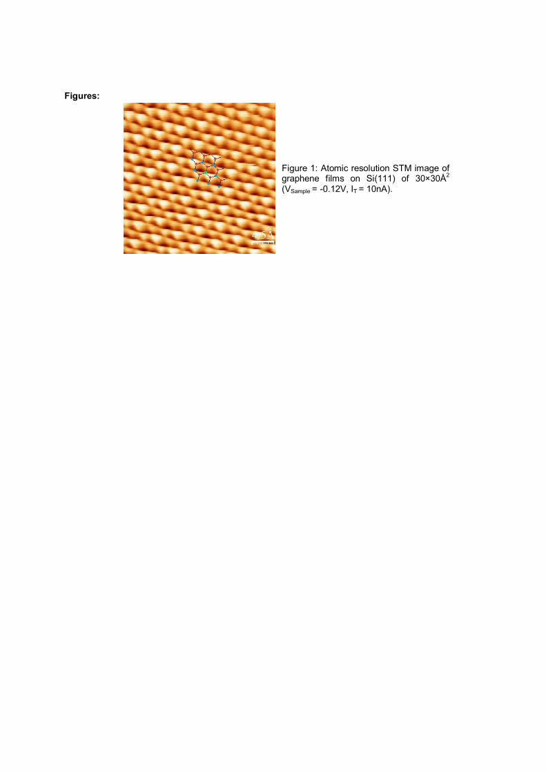
Figures:
Figure 1: Atomic resolution STM image of graphene films on Si(111) of 30×30Å
2
(VSample = -0.12V, IT = 10nA).
Functionalization of CVD Graphene Using Physisorbed
Self-Assembled Monolayers
R. Phillipson1, K.S. Mali
1, I. Asselberghs
2, S. De Gendt
2, S. De Feyter
1
1. Division of Molecular Imaging and Photonics, Department of Chemistry, KU Leuven,
Celestijnenlaan 200F, B-3001 Leuven, Belgium. 2. IMEC, Kapeldreef 75, B-3001 Leuven, Belgium.
[email protected] Abstract Tailoring the electronic properties of graphene in a controlled way is imperative for its use in future
electronic applications. Among several approaches for tailoring the charge carrier concentration, i.e.,
doping graphene, functionalization of the graphene surface using physisorbed organic adsorbates is
advantageous as it does not hamper the charge carrier mobility of graphene. Here we introduce doping
of graphene grown by chemical vapor deposition (CVD) using organic electron donor and acceptor
compounds that self-assemble into 2D networks on the graphene surface. These well ordered networks
offer precise control over the density of molecules on the surface and thus over the graphene surface
properties including doping levels and surface chemistry [1].
The organization of the compounds on the surface of graphite and graphene was characterized using scanning probe microscopy techniques. The doping effect of the self-assembled monolayers was probed via Raman spectroscopy and the electrical characterization of graphene field effect transistors. AFM measurement showed that the compounds can be deposited uniformly on graphite with control over the film thickness down to monolayer coverage. Using high resolution scanning tunneling microscopy (STM) it was shown that the molecules organize in a similar close-packed structures on CVD graphene as seen on graphite. In conclusion, this study is the first step towards tunable and controlled modification of the electronic properties of graphene. References [1] Li, B., A. V. Klekachev, et al, Nanoscale, 5 (2013) 9640-9644

Spin Valve devices on Single and bi-layer CVD-graphene
Luca Pietrobon, Felix Casanova, Luis Hueso
CIC Nanogune, Avenida de Tolosa 76, Donostia – San Sebastian, [email protected]
Abstract Due to the low intrinsic spin-orbit, graphene is a promising material for spintronics. Long spin diffusion lengths
have been experimentally reported for exfoliated [1,2,3] and epitaxial graphene [4,5]. However, the most
promising technique for industrial production of graphene devices remains the Chemical Vapor Deposition (CVD)
one, for which the graphene spintronics literature is not as abundant.
We report on the fabrication of lateral spin valve devices on CVD graphene transferred on SiO2. We show the
importance of an interfacial AlOx layer for spin-injection and confront the performance of single and multi-layer
graphene channels.
References
[1] M. H. D. Guimarães, A. Veligura, P. J. Zomer, T. Maassen, I. J. Vera-Marun, N. Tombros, and B. J. van Wees, Nano Lett. 12, 3512 (2012).
[2] W. Han, K. M. McCreary, K. Pi, W. H. Wang, Y. Li, H. Wen, J. R. Chen, and R. K. Kawakami, J. Magn. Magn. Mater. 324, 369 (2011).
[3] M. Popinciuc, C. Józsa, P. J. Zomer, N. Tombros, A. Veligura, H. T. Jonkman, and B. J. van Wees, Phys. Rev. B 80, 1 (2009).
[4] B. Dlubak, M.-B. Martin, C. Deranlot, B. Servet, S. Xavier, R. Mattana, M. Sprinkle, C. Berger, W. a. De Heer, F. Petroff, A. Anane, P. Seneor, and A. Fert, Nat. Phys. 8, 1 (2012).
[5] T. Maassen, J. J. van den Berg, N. Ijbema, F. Fromm, T. Seyller, R. Yakimova, and B. J. van Wees, Nano Lett. 2, 5 (2012).
Figures
High quality graphite oxide produced by Nacional de Grafite LDTA.
G. M. Trindade1, 2
; F. Vieira2,H. Vespúcio
2; V.S.S.A Ferreira
2; N. G. Rosa
2; C. J, Cook
2; U. B.
Lima2; Marcos A. Pimenta
3, A. P. Santos
1, Clascídia A. Furtado
1, J.P. Nascimento
1
1 Centro de Desenvolvimento da Tecnologia Nuclear, Belo Horizonte, Minas Gerais, 31270-901, Brazil
2 Nacional de Grafite Ltda., Itapecerica, Minas Gerais, 35550-000, Brazil 3Federal University of Minas Gerais, Belo Horizonte, Minas Gerais, 30123-970, Brazil
In this work we are going to show the high quality of the graphite oxide (GO) produced by
Nacional de Grafite LTDA (NGL). It is prepared in a pilot plant with capacity to produce 20
pounds per month. The method was the modified Hummers’s method[1]
and the techniques
used in the characterization were: X Ray Diffraction, BET, Raman, SEM, TEM and XPS.
Graphite oxide, formerly called graphitic oxide or graphitic acid, is a compound
of carbon, oxygen, and hydrogen in variable ratios, obtained by treating graphite with
strong oxidizers. The maximally oxidized bulk product is a yellow solid with C:O ratio between
2.1 and 2.9. The bulk material disperses in basic solutions to produce monomolecular sheets,
known as graphene oxide (fig2). [3]
Graphene oxide sheets have been used to prepare a strong
paper-like material, and have attracted substantial interest as a possible intermediate for the
manufacture of graphene.
Graphite oxide was first prepared by Oxford chemist Benjamin C. Brodie in 1859, treating
graphite with a mixture of potassium chlorate and fuming nitric acid[4]
. In 1957, Hummers and
Offeman developed a safer, quicker, and more efficient process, using a mixture of sulfuric acid
H2SO4, sodium nitrate NaNO3, and potassium permanganate KMnO4, which is still widely used,
often with some modifications.
It should be noted that graphite oxides demonstrate considerable variations of properties
depending on degree of oxidation and synthesis method. For example, temperature point of
explosive exfoliation is generally higher for graphite oxide prepared by Brodie method compared
to Hummers graphite oxide, the difference is up to 100 degrees at the same heating
rates. Hydration and solvation properties of Brodie and Hummers graphite oxides are also
remarkably different.
The structure and properties of graphite oxide are directly related to the synthesis method and
the degree of oxidation. The GO typically preserves the layer structure of the raw material
(natural graphite), although the interlayer spacing becomes two times larger (~0.7 nm). (fig1)
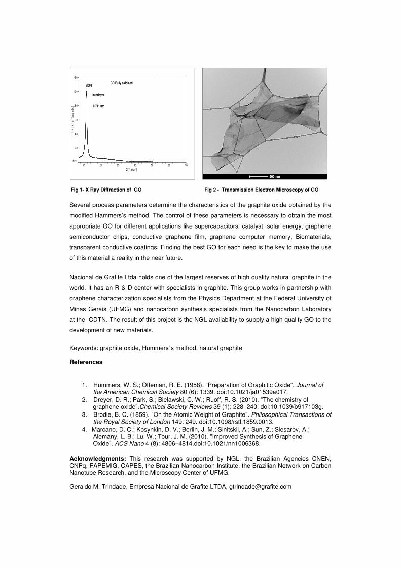
Fig 1- X Ray Diffraction of GO
Several process parameters determine the characteri
modified Hammers’s method. The control of these par
appropriate GO for different applications like
semiconductor chips, conductive graphene film,
transparent conductive coatings.
of this material a reality in the near future.
Nacional de Grafite Ltda holds one of the largest r
world. It has an R & D center with specialists in g
graphene characterization specialists from the Phys
Minas Gerais (UFMG) and nano
at the CDTN. The result of this project is the NGL
development of new materials.
Keywords: graphite oxide, Hummers´s method, natural
References
1. Hummers, W. S.; Offeman, R. E. (1958). "Preparationthe American Chemical Society
2. Dreyer, D. R.; Park, S.; Bielawski, C. W.; Ruoff, Rgraphene oxide".Chemical Society Reviews
3. Brodie, B. C. (1859). "On the Atomic Weight of Graphite"the Royal Society of London
4. Marcano, D. C.; Kosynkin, D. V.; Berlin, J. M.; SinAlemany, L. B.; Lu, W.; Tour, J. M. (2010). "ImprovOxide". ACS Nano 4 (8): 4806
Acknowledgments: This research was supported by NGL, the Brazilian ACNPq, FAPEMIG, CAPES, the Brazilian Nanocarbon InstitutNanotube Research, and the Microscopy Center of UFM
Geraldo M. Trindade, Empresa Nacional de Grafite LT
10 20 30 40 50
2-Theta(°)
x10^3
2.0
4.0
6.0
8.0
10.0
12.0
Inte
ns
ity(C
ou
nts
)
d001
0,711 nm
Interlayer
GO Fully oxidized
X Ray Diffraction of GO Fig 2 - Transmission Electron Microscopy of GO
Several process parameters determine the characteristics of the graphite oxide obtained by the
modified Hammers’s method. The control of these parameters is necessary to obtain the most
appropriate GO for different applications like supercapacitors, catalyst, solar energy, graphene
semiconductor chips, conductive graphene film, graphene computer memory, Biomaterials,
transparent conductive coatings. Finding the best GO for each need is the key to mak
of this material a reality in the near future.
Nacional de Grafite Ltda holds one of the largest reserves of high quality natural graphite in the
world. It has an R & D center with specialists in graphite. This group works in partnership with
graphene characterization specialists from the Physics Department at the Federal University of
nanocarbon synthesis specialists from the Nanocarbon La
at the CDTN. The result of this project is the NGL availability to supply a high quality GO to the
eywords: graphite oxide, Hummers´s method, natural graphite
Hummers, W. S.; Offeman, R. E. (1958). "Preparation of Graphitic Oxide". Journal of the American Chemical Society 80 (6): 1339. doi:10.1021/ja01539a017.
Dreyer, D. R.; Park, S.; Bielawski, C. W.; Ruoff, R. S. (2010). "The chemistry of .Chemical Society Reviews 39 (1): 228–240. doi:10.1039/b917103g
"On the Atomic Weight of Graphite". Philosophical Transactions of the Royal Society of London 149: 249. doi:10.1098/rstl.1859.0013.
Marcano, D. C.; Kosynkin, D. V.; Berlin, J. M.; Sinitskii, A.; Sun, Z.; Slesarev, A.; Alemany, L. B.; Lu, W.; Tour, J. M. (2010). "Improved Synthesis of Graphene
(8): 4806–4814.doi:10.1021/nn1006368.
This research was supported by NGL, the Brazilian Agencies CNEN, , FAPEMIG, CAPES, the Brazilian Nanocarbon Institute, the Brazilian Network on Carbon
Nanotube Research, and the Microscopy Center of UFMG.
Geraldo M. Trindade, Empresa Nacional de Grafite LTDA, [email protected]
60 70
Transmission Electron Microscopy of GO
stics of the graphite oxide obtained by the
ameters is necessary to obtain the most
st, solar energy, graphene
graphene computer memory, Biomaterials,
Finding the best GO for each need is the key to make the use
eserves of high quality natural graphite in the
raphite. This group works in partnership with
tment at the Federal University of
carbon synthesis specialists from the Nanocarbon Laboratory
availability to supply a high quality GO to the
Journal of
. S. (2010). "The chemistry of 10.1039/b917103g.
Philosophical Transactions of
itskii, A.; Sun, Z.; Slesarev, A.; ed Synthesis of Graphene
gencies CNEN, e, the Brazilian Network on Carbon

Expanded graphite as a reinforcing filler in elastomer technology
Martyna Pingot, Marian Zaborski
Lodz University of Technology, Institute of Polymer and Dye Technology, Stefanowskiego 12/16, Lodz, Poland
Contact: [email protected]
Abstract
Graphite is a layered material, which consists of a graphene structures where carbon atoms are
bound by covalent bonds to other carbons in the same plane and only van der Waals forces are acting
between successive layers. Since the van der Waals forces are relatively weak, it is possible for a wide
range of atoms, molecules, and ions to intercalate between graphite sheets. Conventional natural
graphite are usually micro-diameter powders. In order to make a composite with satisfactory properties,
loadings of filler are usually as high as 20 wt% or even higher. This often results in a material with poor
mechanical properties and high density. In order to obtain improved mechanical, thermal and electrical
conductive properties the synthesis of expanded graphite was developed.[1-3]
Natural graphite is first
converted to intercalated or expandable graphite through chemical oxidation in the presence of
concentrated sulfuric acid and nitric acid (4:1, v/v). Expanded graphite is then obtained by rapid
expansion and exfoliation of expandable graphite in a furnace above 6000C.
[4,5]
The aim of presented work was to obtain elastomer composites exhibiting high mechanical
properties, improved air permeability and electrical conductive properties. The expanded graphite was
obtained from acid intercalated graphite Grafguard 160-80N (Graftech) by the means of thermal
expansion at high temperature. As an elastomer matrix the acrylonitrile-butadiene rubber (NBR) was
used. In order to improve dispersion of the filler, several types of dispersing agents were used: anionic,
cationic, nonionic and ionic liquids. The fillers were characterized by dibutylphtalate absorption analysis,
aggregates size and rheological properties of filler suspensions. The compounding was carried out in a
laboratory Brabender Mixer. Samples were prepared through the vulcanization process at 1600C. The
vulcanization kinetics of rubber compounds, crosslink density, mechanical properties, hysteresis under
stretching, conductive properties of vulcanizates and the Payne effect analysis under shearing were
also measured. In order to characterize filler dispersion in elastomer matrix the SEM images were
obtained (Fig. 1). To enhance the degree of interphase boundary, the graphite layers separation was
conducted in polar solvents by the means of ultrasonic waves. As a result the partial graphite exfoliation
was observed. The estimated thickness of stacked graphene layers is below 50 nm.
References
[1] Chen G., Wu D., Weng W., Carbon, 41 (2003) 579.
[2] Saunders D.S., Galea S.C., Deirmendjian G.K., Composite, 24(4) (1993) 309.
[3] Ezquerra Y.A., Kulescza M., Alta-Calleja F.J., Synth Met., 41 43 (1991) 915.
[4] Yasmin A., Luo J.J., Daniel I.M., Compos. Sci. Technol., 66 (2006) 1182.
[5] Drzal L.T., Fukushima H., Polym. Prep., 42(2) (2001) 42.

Fig.1. SEM image of NBR composite containing 10 phr of expanded graphite showing the intercalated
graphite layers with elastomer matrix.
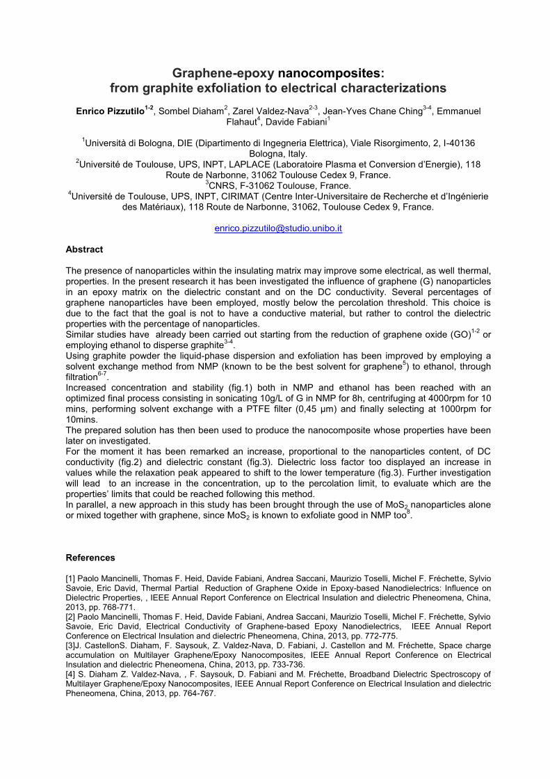
Graphene-epoxy nanocomposites: from graphite exfoliation to electrical characterizations
Enrico Pizzutilo
1-2, Sombel Diaham
2, Zarel Valdez-Nava
2-3, Jean-Yves Chane Ching
3-4, Emmanuel
Flahaut4, Davide Fabiani
1
1Università di Bologna, DIE (Dipartimento di Ingegneria Elettrica), Viale Risorgimento, 2, I-40136
Bologna, Italy. 2
Route de Narbonne, 31062 Toulouse Cedex 9, France. 3CNRS, F-31062 Toulouse, France.
4Université de Toulouse, UPS, INPT, CIRIMAT (Centre Inter-
des Matériaux), 118 Route de Narbonne, 31062, Toulouse Cedex 9, France.
Abstract The presence of nanoparticles within the insulating matrix may improve some electrical, as well thermal, properties. In the present research it has been investigated the influence of graphene (G) nanoparticles in an epoxy matrix on the dielectric constant and on the DC conductivity. Several percentages of graphene nanoparticles have been employed, mostly below the percolation threshold. This choice is due to the fact that the goal is not to have a conductive material, but rather to control the dielectric properties with the percentage of nanoparticles. Similar studies have already been carried out starting from the reduction of graphene oxide (GO)
1-2 or
employing ethanol to disperse graphite3-4
. Using graphite powder the liquid-phase dispersion and exfoliation has been improved by employing a solvent exchange method from NMP (known to be the best solvent for graphene
5) to ethanol, through
filtration6-7
. Increased concentration and stability (fig.1) both in NMP and ethanol has been reached with an optimized final process consisting in sonicating 10g/L of G in NMP for 8h, centrifuging at 4000rpm for 10 mins, performing ly selecting at 1000rpm for 10mins. The prepared solution has then been used to produce the nanocomposite whose properties have been later on investigated. For the moment it has been remarked an increase, proportional to the nanoparticles content, of DC conductivity (fig.2) and dielectric constant (fig.3). Dielectric loss factor too displayed an increase in values while the relaxation peak appeared to shift to the lower temperature (fig.3). Further investigation will lead to an increase in the concentration, up to the percolation limit, to evaluate which are the properties limits that could be reached following this method. In parallel, a new approach in this study has been brought through the use of MoS2 nanoparticles alone or mixed together with graphene, since MoS2 is known to exfoliate good in NMP too
8.
References [1] Paolo Mancinelli, Thomas F. Heid, Davide Fabiani, Andrea Saccani, Maurizio Toselli, Michel F. Fréchette, Sylvio Savoie, Eric David, Thermal Partial Reduction of Graphene Oxide in Epoxy-based Nanodielectrics: Influence on Dielectric Properties, , IEEE Annual Report Conference on Electrical Insulation and dielectric Pheneomena, China, 2013, pp. 768-771. [2] Paolo Mancinelli, Thomas F. Heid, Davide Fabiani, Andrea Saccani, Maurizio Toselli, Michel F. Fréchette, Sylvio Savoie, Eric David, Electrical Conductivity of Graphene-based Epoxy Nanodielectrics, IEEE Annual Report Conference on Electrical Insulation and dielectric Pheneomena, China, 2013, pp. 772-775. [3]J. CastellonS. Diaham, F. Saysouk, Z. Valdez-Nava, D. Fabiani, J. Castellon and M. Fréchette, Space charge accumulation on Multilayer Graphene/Epoxy Nanocomposites, IEEE Annual Report Conference on Electrical Insulation and dielectric Pheneomena, China, 2013, pp. 733-736. [4] S. Diaham Z. Valdez-Nava, , F. Saysouk, D. Fabiani and M. Fréchette, Broadband Dielectric Spectroscopy of Multilayer Graphene/Epoxy Nanocomposites, IEEE Annual Report Conference on Electrical Insulation and dielectric Pheneomena, China, 2013, pp. 764-767.
[5] Yecnny Hernandez, Mustafa Lotya, David Rickard, Shane D. Bergin, and Jonathan N. Coleman, Measurement of multicomponents Solubility Parameters for Graphene Facilitates Solvent Discovery, Langmuir, 2010, pp. 3208-3213 [6] Xiaoyan Zhang, Anthony C. Coleman, Nathalie Katsonis, Wesley R. Browne, Bart J. Van Wees and Ben L. Feringa, Dispersion of graphene in ethanol using a simple solvent exchange method, Chemical Communications, 2010, 46, 7539-7541
-Exfoliated Graphene at Extremely High Concentration, Langmuir, 2011, 27, pp. 9077-9082.
Coleman, Preparation of High Concentration Dispersion of Exfoliated MoS2 with increased flake size, Chemestry of Materials, 2012, 24, pp. 2414-2421.
Figures
0 2 4 6 8 10 12 14 16 18
0,1
0,2
0,3
0,4
0,5
0,6
0,7
0,8
Cf
(mg
/mL
)
Ts(h)
10g/L
5g/L
1g/L
1h 2h 4h 8h 16h
160
180
200
220
240
260
280 Size (d.nm)
Zeta Potential (mV)
Ts (h)
Siz
e (
d.n
m)
-50
-48
-46
-44
-42
-40
-38
-36
-34
-32
-30
-28
-26
-24
-22
-20
Zeta
Po
tentia
l (m
V)
NO SEL 1000rpm 2000rpm 4000rpm AFE
150
200
250
300
350
400
450
500
550
Size (d.nm)
Zeta Potential (mV)
Selection
Siz
e (
d.n
m)
-50
-48
-46
-44
-42
-40
-38
-36
Zeta
Po
tentia
l (m
V)
Fig.1 Final concentration, Cf, in NMP with different sonication time and different initial concentration (a); particle size and zeta
potential with sonication time (b) and with selection till exchange in Ethanol, AFE (b) starting from 10g/L with a sonication time of 8h (optimized).
3k 4k 5k 6k 7k 8k 9k 10k
1E-15
1,5E-15
2E-15
2,5E-15
3E-15
NEAT
G 0,05wt%
G 0,24wt%
Sig
ma
(S
/m)
V/mm
Fig.2 DC conductivity for tested specimens with increasing nanoparticles content (below percolation).
-200 -150 -100 -50 0 50 100 150 200 250
101
102
103
104
105
Eps'0
.1H
z
Temp. [°C]
NEAT
G 0,02wt%
G 0,05wt%
G 0,24wt%
-200 -150 -100 -50 0 50 100 150 200 250
101
102
103
104
105
Eps'0
.1H
z
Temp. [°C]
NEAT
MoS2 0,153wt%
G0,026wt%/MoS2
(50/50v%)
G0,058wt%/MoS2
(75/25v%)
) at 0,1Hz in the range [-150-200°C] for graphene nanocompostites (left) and graphene/MoS2
nanocomposites (right)
-200 -150 -100 -50 0 50 100 150 200 250
10-3
10-2
10-1
100
101
TanD
0,1
Hz
Temp. [°C]
NEAT
G 0,02wt%
G 0,05wt%
G 0,24wt%
MoS2 0,15wt%
G0,026wt%/MoS2
(50/50v%)
G0,058wt%/MoS2
(75/25v%)
Fig.4 Loss Factor (TanD) at 0,1Hz in the range [-150-200°C] for graphene and graphene/MoS2 nanocomposites
a b c
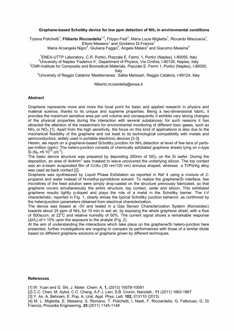
Graphene-based Schottky device for low ppm detection of NH3 in environmental conditions
Tiziana Polichetti1, Filiberto Ricciardella
1,2, Filippo Fedi
3, Maria Lucia Miglietta
1, Riccardo Miscioscia
1,
Ettore Massera1 and Girolamo Di Francia
1
Maria Arcangela Nigro4, Giuliana Faggio
4, Angela Malara
4 and Giacomo Messina
4
1ENEA-UTTP Laboratory, C.R. Portici, Piazzale E. Fermi, 1, Portici (Naples), I-80055, Italy
2University of Naples , Department of Physics, Via Cinthia, I-80126, Naples, Italy
3CNR-Institute for Composite and Biomedical Materials, Piazzale E. Fermi 1, Portici (Naples), I-80055,
Italy 4
Calabria, I-89124, Italy
[email protected] Abstract Graphene represents more and more the focal point for basic and applied research in physics and material science, thanks to its unique and supreme properties. Being a two-dimensional fabric, it provides the maximum sensitive area per unit volume and consequently it exhibits very strong changes of the physical properties during the interaction with several substances; for such reasons it has attracted the attention of the researchers for environmental monitoring of different toxic gases, such as NH3 or NO2 [1]. Apart from the high sensitivity, the focus on this kind of applications is also due to the mechanical flexibility of the graphene and not least to its technological compatibility with metals and semiconductors, widely used in portable electronic devices [2-3]. Herein, we report on a graphene-based Schottky junction for NH3 detection at level of few tens of parts-per-million (ppm). The hetero-junction consists of chemically exfoliated graphene sheets lying on n-type Si (ND
15 cm
-3).
The basic device structure was prepared by depositing 250nm of SiO2 on the Si wafer. During the deposition, an area of 4x4mm
2 was masked to leave uncovered the underlying silicon. The top contact
was an e-beam evaporated film of Cr/Au (30 nm/120 nm) annulus shaped, whereas a Ti/Pd/Ag alloy was used as back contact [2]. Graphene was synthesized by Liquid Phase Exfoliation as reported in Ref 4 using a mixture of 2-propanol and water instead of N-methyl-pyrrolidone solvent. To realize the graphene/Si interface, few microlitres of the feed solution were simply drop-casted on the structure previously fabricated, so that graphene covers simultaneously the entire structure, top contact, oxide and silicon. This exfoliated graphene results lightly p-doped and plays the role of a metal in the Schottky barrier. The I-V characteristic, reported in Fig. 1, clearly shows the typical Schottky junction behavior, as confirmed by the heterojunction parameters obtained from electrical characterization. The device was biased at -3V and tested in a Gas Sensor Characterization System (Kenosistec) towards about 25 ppm of NH3 for 10 min in wet air, by exposing the whole graphene sheet, with a flow of 500sccm, at 22
oC and relative humidity of 50%. The current signal shows a remarkable response
0) of 10% upon the exposure to the analyte (Fig. 2). At the aim of understanding the interactions which take place on the graphene/Si hetero-junction here presented, further investigations are ongoing to compare its performances with those of a similar diode based on different graphene solutions or graphene grown by different techniques. References [1] W. Yuan and G. Shi, J. Mater. Chem. A, 1, (2013) 10078-10091 [2] C.C. Chen, M. Aykol, C.C. Chang, A.F.J. Levi, S.B. Cronin, Nanolett., 11 (2011) 1863-1867 [3] Y. An, A. Behnam, E .Pop, A. Ural, Appl. Phys. Lett. 102, 013110 (2013) [4] M. L. Miglietta, E. Massera, S. Romano, T. Polichetti, I. Nasti, F. Ricciardella, G. Fattoruso, G. Di Francia, Procedia Engineering, 25 (2011) 1145-1148
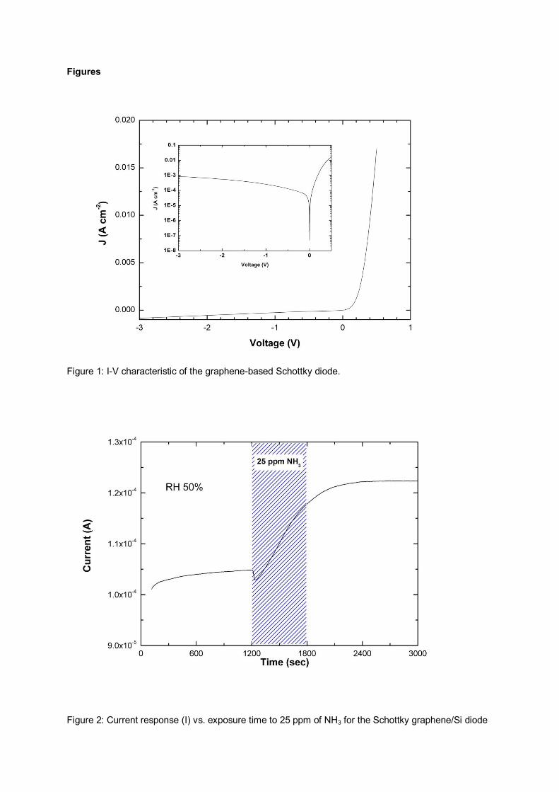
Figures
Figure 1: I-V characteristic of the graphene-based Schottky diode.
Figure 2: Current response (I) vs. exposure time to 25 ppm of NH3 for the Schottky graphene/Si diode
A large scale systematic study of graphene/metal contact resistance using cTLM
Maria Politou1,2,*
, Enlong Liu1,2
, Inge Asselberghs1,2
, ChangSeung Lee3, Koen Martens
1,2, Iuliana
Radu1,2
, Zsolt Tokei1, Cedric Huyghebaert
1, Stefan De Gendt
1,2, Marc Heyns
1,2
1imec, Kapeldreef 75, 3001 Leuven, Belgium
2KU Leuven, 3001 Leuven, Belgium
3SAIT, Samsung Electronics Co., Yongin 446-712, South Korea
Abstract In this work, a systematic study of the graphene/metal contact resistance (RC) is conducted. The circular Transfer Length Method (cTLM) is used to determine the RC values with several metals. Samples with Cu, Ti, Ni, Pt, Ag, Pd and Au contacts were fabricated and electrically characterized. Our results indicate that noble metals show lower RC. The lowest RC was observed for Au samples (~2.3k . m). Further improvement of contact is observed after a high temperature (300
oC) anneal in Ar.
Introduction Graphene is one of the candidates for post-Si electronics. It is actively being investigated both for channel and interconnect applications. One common concern is contact engineering. The effect of the metal contacts on graphene and the contact resistance (RC) values measured are important topics not only for graphene device performance but also for hybrid graphene/metal interconnects. Contact resistance has to be as low as possible. 80 . m is the state-of-the-art demand in Si devices [1]. Ohmic contacts, without rectifying characteristics, are desirable. The voltage drop over the contact should be small, to provide enough current to the device [2]. Reported RC values show large scatter ranging from hundreds to tens of thousands . m. The results depend on the graphene type (exfoliated, CVD grown, epitaxially grown), the fabrication and post-fabrication treatments and the metal used. Apart from the metal work function, factors such as cleanliness, metal quality, wettability, grain size, roughness and edge vs. surface contacts may play a role [1, 3-7]. The aim of this work is to develop a systematic approach to process, characterize samples and analyze data. The goal is understanding and tuning the graphene/metal interface towards lower RC values. Experimental In this work CVD (Chemical Vapor Deposition) grown graphene was used as it is the most suitable for large scale technological applications. Graphene was transferred onto a Si/SiO2 substrate. To determine RC, the circular Transfer Length Method (cTLM) [2, 8] was used with a series of different metals. As only one lithography step is required to deposit the metal
contacts, cTLM is a fast and efficient method. Moreover, because of the circular configuration current spreading effects are limited. cTLM structures were fabricated with photolithography on 2x2cm
2 graphene samples.
An optical image of the fabricated structures is shown in Fig. 1. One structure consists of 12 circular electrode configurations (inner and outer) with electrode spacing ranging from 1 m up to 32 m. The radius of the inner electrode is 50 m. Special focus was given on collecting statistical data for every case, thus 72 cTLM structures were fabricated and characterized on the same sample. cTLM samples were fabricated and electrically characterized with Cu, Ti, Ni, Pt, Ag, Pd and Au contacts. 50nm of metal were deposited for Cu, Ni, Pt, Pd and Au. 30 nm of Ti or Ag with a capping layer 20nm of Pd or Au were also investigated. Capping layers were used to prevent contact oxidation. The sample denoted (Ti)/Pd was fabricated with 1nm of Ti and 50nm of Pd. This metal stack was investigated as Ti is known to improve adhesion for Pd contacts. Id - Vd curves were measured at room temperature (25
oC) using a Suss+MicroTec
PA300 wafer prober and an Agilent 4156C parameter analyzer. Before measuring, all samples were annealed at 150
oC in N2 for 1 hour
to reduce the effect of the ambient conditions. Based on the calculated total resistance and using the cTLM, contact and sheet resistance (RS) values were extracted. We have also investigated the effect of annealing at higher temperatures. Samples were annealed at 300
oC in Ar for 1 hour before electrical
characterization. Results and discussion Average RC and RS values extracted for different metals are shown in Fig. 2a and 2b respectively. The average is performed on values from up to 72 structures. Error bars represent standard deviation. Noble metals such as Pt, Ag, Pd, Au show lower RC compared to Cu and Ti. Ni is the only non-noble metal that produces a contact resistance comparable to that of the noble metal. A possible explanation is metal oxidation at the interface with graphene. Further physical characterization of the interface is ongoing. The lowest RC was observed for Au samples (~2.3k . m). Ti/Au (30nm Ti, 20nm Au) and

Ti/Pd (30nm Ti, 20nm Pd) samples resulted in similar RC values, this being an indication that the capping metal has no effect on RC. The comparison between (Ti)/Pd (1nm Ti, 50nm Pd) and Ti/Pd (30nm Ti, 20nm Pd) indicates that the contact degrades with a higher amount of Ti present. Most probably in the (Ti)/Pd case a Pd contact to graphene is effectively formed. Extracted RS values (Fig. 2b) are approximately independent of the metal used. The average RS extracted is ~1.8k . In Fig. 3a and 3b the results of annealing at higher temperatures can be seen for Cu, Ti and Pd. In all cases large improvements in the extracted RC values were observed after annealing (Fig. 3a). The largest improvement of ~92% was observed for Cu. The RS values extracted (Fig. 3b) were approximately similar before and after annealing, indicating that the overall improvement comes from a reduced contact resistance. Conclusion We have applied a systematic approach for comparing the contact resistance between graphene and several metals. We have used the same graphene type, fabrication conditions and characterization methods for all metals. To collect statistical data, we have performed measurements over large device sets. Our results indicate that noble metals show lower RC. This suggests possible oxidation of non-noble metals at the interface with graphene. Annealing at 300
oC in Ar lowers the contact resistance
values. Acknowledgements All current and former members of the imec 2D Materials Team are acknowledged for their help, support and fruitful discussions. References [1] J. T. Smith et al., ACS Nano, 7(2013) 36613667 [2] D. K. Schroder, Semiconductor material and device characterization, 3
rd -
Intersc 2006 [3] F. Xia et al., Nat. Nanotech., 6(2011) 179-184 [4] E. Watanabe et al., Diamond&Related Materials, 24 (2012) 171-174 [5] S. M. Song et al., Nanoletters, 12(2012) 3887-3892 [6] O. Balci, C. Kocabas, Appl. Phys. Lett., 101 243105(2012) [7] L. Wang et al., Science, 342 (2013) 614-617 [8] J. H. Klootwijk, C.E. Timmering, Proc.IEEE 2004, ICMTS, 17(2004) 247-252 Figures
Figure 1. An optical image of
the fabricated cTLM structures.
Figure 2. a) RC values extracted for various metal contacts. All noble metals show lower RC with Au samples showing the lowest (~2.3k . m). Samples with Ni contacts also have a low RC. b) RS values extracted for various metal contacts. Similar RS of about 1.8k in average is extracted, independent of the metal used.
Figure 3. a) RC values before and after annealing at 300
oC in
Ar for 1 hour. Large improvements were observed after annealing in all cases. b) RS values before and after annealing at 300
oC in Ar for 1 hour. Values are similar before
and after annealing, indicating that the overall improvement comes from a reduced contact resistance.

Quantitatively characterising the size of graphene defects with Raman spectroscopy
Andrew J. Pollard, Helena Stec, Bonnie J. Tyler, Alex G. Shard, Ian S. Gilmore, Debdulal Roy
National Physical Laboratory, Hampton Road, Teddington, TW2 5BY, UK
Abstract The huge potential of graphene to disrupt many different application areas of technology has been extensively shown in research laboratories over the last decade and has now led to the beginning of an adoption of this 2-D material in industry worldwide. However, the requirement to overcome the practical problems related to 2-D materials, such as quality, reproducibility and contamination, increasingly needs to be met. At the same time, companies in the emerging graphene industry require the ability to accurately, quantitatively and reliably characterise these types of materials to instil market confidence. Raman spectroscopy has been shown to rapidly characterise many different attributes of graphene in a non-destructive manner, attributes such as the number and orientation of layers, strain effects and doping [1]. Raman spectroscopy is arguably also the metrological tool of choice for quantifying the
graphene and affects many of the supreme properties of graphene that would be important in areas ranging from electronics to filtering. Raman spectroscopy has already been shown to be invaluable in determining the defect density in graphene, as the ratio of the D- and G-peaks varies in relation to the graphene inter-defect distance, LD [2,3]. However, this intensity ratio also varies in relation to the graphene defect size, and although this relationship has been mathematically described, it has not been shown experimentally. By introducing vacancy defects into pristine single-layers of graphene using different bismuth and manganese ions, we show the variation in the D- and G-peak intensity ratios with increasing defect size, as shown in Figure 1. The relationship between defect density, size and the phase-breaking length of graphene (the average distance travelled by the photoexcited electron-hole pair during its life-time), L , can be described, and L can be calculated with an accuracy not previously achieved. Scanning tunnelling microscopy (STM) measurements of these introduced defects have also been performed to corroborate these Raman spectroscopy results, as shown in Figure 2. References [1] Ferrari and Basko, Nat. Nanotech. 8 (2013) 235 [2] Lucchese et al., Carbon 48 (2010) 1592 [3] Cancado et al., Nano Lett. 11 (2011) 3190
Figures
Figure 1: Intensity ratio of Raman D- and G-peaks vs. the average inter-defect distance, LD, for different size defects in a single-layer of graphene
Figure 2: STM image of a defect in a graphitic lattice created by manganese ion bombardment, with scale bars in nanometres

Injection moldable electrostatic dissipative composites based on polycarbonate/oxygen-plasma treated graphene nanoplatelet/multi-walled carbon nanotube Akkachai Poosala
1,a, Kittipong Hrimchum
2,b, Darunee Aussawasathien
2,c*
and Duanghathai Pentrakoon3,d*
1Technopreneurship and Innovation Management, Graduate School, Chulalongkorn University
Bangkok 10330, Thailand 2Plastics Technology Lab, Polymer Research Unit, National Metal and Materials Technology Center,
Pathumthani 12120, Thailand 3Department of Materials Science, Faculty of science, Chulalongkorn University
Bangkok 10330 Thailand
*Corresponding authors:
Present author: [email protected]
Abstract Electronic components are susceptible to damage from electrostatic discharge (ESD). The annual losses in products containing sensitive electronic components and subassemblies due to ESD during manufacturing, assembly, storage and shipping has been estimated in billions of dollars [1]. In order to reach savings of billions of dollars, an ESD control system should be introduced in production and handling. Electrostatic dissipative materials are often used to slow down the charge removal process and prevent a damaging ESD event during storage and shipping. For many articles in ESD
protected environments the optimal surface resistivity is in the range of 105-10
9 /sq [2, 3].
Electrostatic dissipating thermoplastic composites have successfully eliminated ESD failures in many applications in the electronics industry. A number of conductive fillers are presently available to material engineers, including carbon black (CB), carbon fibers (CF), metallic powders, flakes or fibers, and glass spheres or glass fibers coated with metals. For a given polymeric composite, electrical conductivity is determined by the amount, type and shape of the conductive fillers [4-6]. Carbon black-loaded static controlling products usually contain 15-20% CB by weight (wt%). This relatively high CB concentration causes local variation of the concentration of the conductive additives resulting in variation of the conductivity with location in the same product. The addition of carbon black at increasing levels has a negative effect on the processability of a composite and its mechanical properties: the melt viscosity increases and the impact resistance decreases. Contamination is also an important issue since, in highly filled CB composites, the carbon powder tends to slough and thus contaminate the environment. There is therefore a challenge in developing cleaner injection moldable composites with consistent and uniform surface resistivity in the static dissipative range.
Carbon nanotube (CNT) with a cylindrical nanostructure and graphene with a two-dimensional sheet of sp
2-hybridized carbon atoms densely packed in a honeycomb network have distinctly
different geometry shape; but they have remarkable properties, such as superior thermal and mechanical properties and exceptional electronic transport [3-8], which make them excellent candidates as reinforcing and conducting fillers in composites. In this research work, we are doing a technology edge which will replace the material of ESD composites from high loading CB to a small amount of conductive fillers using oxygen-plasma treated graphene nanoplatelet (OGNP)/multi-walled carbon nanotube (MWCNT) hybrid system, which will eliminate the contamination problem and provide permanent ESD properties including high mechanical properties. Injection moldable composites with desired resistivities in the ESD range (10
5-
109 /sq) for conveying in production lines, storage, shipment and for cleanroom applications, having
good and balanced mechanical properties can be achieved by combining PC resin with 1.0-2.0 wt% OGNP and 2.0 wt% MWCNT as shown in Table 1. Such PC/OGNP/MWCNT composites will be suitable for making ESD containers (see Fig. 1) generally used in electronic and semiconductor and hard disk drive industries. References [1] S.P. Singh, H. El-Khateeb, Packaging Technology Science, Vol. 7 (1994) p.283. [2] K. Vakiparta, EOS/ESD Symposium, Phonix AZ, (1995) p.229. [3] R.W. Cambell, W. Tan, EOS/ESD Symposium,Phoenix AZ, (1995) p.218. [4] M. Narkis, A. Ram, F. Flashner, Journal of Applied Polymer Science, Vol. 22 (1978) p.1163. [5] M. Narkis, A. Ram, Z. Stein, Journal of Applied Polymer Science, Vol 25 (1980) p.1515. [6] M. Narkis, A. Vaxman, Journal of Applied Polymer Science, Vol. 29 (1984) p.1639. [7] P.G. Collins and P. Avouris, Scientific American Magazine, Vol. 283 (2000) p. 62. [8] J. Nilsson, A.C. Neto, F. Guinea and N. Peres, Physical Review Letters, Vol. 97 (2006) p. 266. [9] A.A. Balandin, S. Ghosh, W. Bao, I. Calizo, D. Teweldebrhan and F. Miao, Nano Letters, Vol. 8 (2008), p. 902.

[10] M. Poot and H.S. Van der Zant: Applied Physics Letters, Vol. 92 (2008), p. 111. [11] M. Dresselhaus, G. Dresselhaus, J. Charlier and E. Hernandez: Philos. T. Roy. Journal of the
Chemical Society A, Vol. 362 (2004), p. 2065. [12] R.S. Ruoff and D.C. Lorents: Carbon, Vol. 33 (1995), p. 925.
Table 1 Properties of PC/OGNP/MWCNT composites
Samples Properties
A
B
Tensile strength (psi) 8554 8608
Tensile modulus (psi) 0.33x10⁶ 0.36x10
6
Tensile elongation (%) 10.00 10.00
Flexural Strength (psi) 11178 12541
Flexural modulus (psi) 0.29x10⁶ 0.32x10
6
Izod notched (ft.lb/in) 1.24 1.27
Izod unnotched (ft.lb/in) 40.35 N 37.34 N
Shrinkage (in/in) 0.0070 0.0057
Specific gravity 1.18 1.19
Melt index 7.60 19.69
Volume resistivity (Ohm·cm) 5.28x10⁷
9.04x10⁵
Surface resistivity Point to Point (Ohm/sq) 1.05 x10⁸
1.10x10⁶
Surface resistivity Point to Ground (Ohm/sq)
1.6 x10⁵ 1.15x10
5
Graphene dosage (wt%) 2 1
MWCNT dosage (wt%) 2 2
Type of compatibilizer Methyl methacrylate butadiene styrene
(MBS)
Methyl methacrylate butadiene styrene
(MBS)
Compatibilizer dosage (wt%) 0.5 0.5
Fig. 1 ESD trays used in semiconductor and hard disk drive industries.

Electronic transport in disordered graphene antidot lattice devices
Stephen R. Power, Antti-Pekka Jauho
Center for Nanostructured Graphene (CNG), DTU Nanotech, Technical University of Denmark, 2800 Kongens Lyngby, Denmark
Abstract Much recent effort in graphene research has focused on attempts to introduce a bandgap into
the otherwise semi-metallic electronic band structure of graphene. Such a feature would allow the integration of graphene, with its many superlative physical, electronic, thermal and optical properties, into a wide range of conventional device applications. In particular, the presence of a bandgap is a vital step in the development of a graphene transistor capable of competing with standard semiconductor-based devices.
Initial investigations were primarily based around graphene nanoribbons[1], with the electron confinement induced by the presence of crystalline edges predicted to introduce a bandgap similar to that found in many carbon nanotubes. More recent efforts have turned towards graphene superlattices, where the imposition of a periodic perturbation of the graphene sheet is also predicted to open up a bandgap. The periodic perforation of a graphene sheet, to form a so-called graphene antidot lattice (GAL), is one such implementation of the latter technique [2].
Theoretical studies of GAL-based systems have suggested that the bandgap behaviour in many cases follows a simple scaling law relating the period of the perturbation and the antidote size [2].Furthermore, it is predicted that only a small number of antidot rows are required to induce bulk-like transport gaps, suggesting the use of GALs in finite barrier systems which do not suffer from the Klein-tunnelling driven barrier leakage expected for gated systems [3]. Indeed, the potential barrier efficacy of GALs has led to predicted applications in the wave-guiding of charge carriers, in analogy with photonic crystals where antidot lattice geometries are also considered [4].
However, many of these potential devices applications are predicated on atomically precise graphene antidot devices, whereas experimental fabrication (primarily involving block copolymer or electron beam lithography techniques [5]) will inevitably introduce a degree of imperfection and disorder into the system. Much like the properties of nanoribbons were found to be greatly affected by disorder[6], recent studies suggest that the electronic and optical properties of GALs may also be strongly perturbed [7]. We should therefore expect that the transport properties and device fidelity of the systems described above will depend on the degree of disorder present in the antidot lattice
Motivated by this concern we have simulated a wide range of finite GAL devices, in both simple-barrier and waveguide geometries, with various disorder types and strengths [8]. We find that the geometries predicted to give the largest bandgaps, namely those with a dense array of small holes, are particularly susceptible to the effects of disorder and that transport gaps are quickly quenched as leakage channels form at energies in the bandgap. Geometric disorder, consisting of fluctuations in the positions and sizes of the antidots, is found to have a particularly dramatic effect (see Figure 1).However, the signatures of such disorders are found to be strongly dependent on the edge geometry of individual antidots, and different behaviour is observed when the antidot edge atoms have armchair or zigzag configurations, or alternating sequences of both. Recent experimental progress [9] in controlling the edge geometry of perforations in graphene suggests that, even in the presence of disorder, the properties of GAL systems may be manipulated in order to produce devices with desirable electronic transport properties.
References[1] Son et al, Phys. Rev. Lett. 97 (2006) 216803[2] Pedersen et al, Phys. Rev. Lett. 100 (2008) 136804[3] Gunst et al, Phys. Rev. B 84 (2011) 155449[4] Pedersen et al, Phys. Rev. B 86 (2012) 245410[5] Eroms and Weiss, New J. Phys. 11 (2009) 095021, Kim et al, Nano. Lett. 10 (2010) 1125[6] Mucciolo et al, Phys. Rev. B 79 (2009) 075407[7] Yuan et al, Phys. Rev. B 87 (2013) 085430, Yuan et al, Phys. Rev. B 88 (2013) 195401[8] Power and Jauho, in preparation.[9] Oberhauer et al, Appl. Phys. Lett. 103 (2013) 143111, Jia et al, Science 323 (2009) 1701

Figures
Figure 1: a) Schematic of an antidot barrier in a wide nanotibbon with perfect periodicity (black circles) and with a small position disorder (red dashed circles). b) The conductance calculated through both systems. The bandgap in the range 0 - 0.33eV in the perfect system (black line) is clearly washed out in the disordered case (red dashed line).
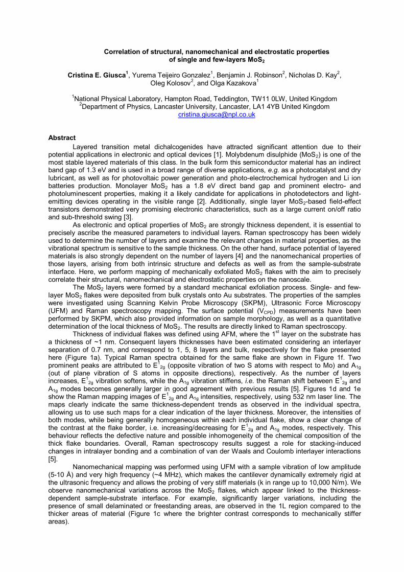
Correlation of structural, nanomechanical and electrostatic properties of single and few-layers MoS2
Cristina E. Giusca
1, Yurema Teijeiro Gonzalez
1, Benjamin J. Robinson
2, Nicholas D. Kay
2,
Oleg Kolosov2, and Olga Kazakova
1
1National Physical Laboratory, Hampton Road, Teddington, TW11 0LW, United Kingdom
2Department of Physics, Lancaster University, Lancaster, LA1 4YB United Kingdom
Abstract
Layered transition metal dichalcogenides have attracted significant attention due to their potential applications in electronic and optical devices [1]. Molybdenum disulphide (MoS2) is one of the most stable layered materials of this class. In the bulk form this semiconductor material has an indirect band gap of 1.3 eV and is used in a broad range of diverse applications, e.g. as a photocatalyst and dry lubricant, as well as for photovoltaic power generation and photo-electrochemical hydrogen and Li ion batteries production. Monolayer MoS2 has a 1.8 eV direct band gap and prominent electro- and photoluminescent properties, making it a likely candidate for applications in photodetectors and light-emitting devices operating in the visible range [2]. Additionally, single layer MoS2-based field-effect transistors demonstrated very promising electronic characteristics, such as a large current on/off ratio and sub-threshold swing [3].
As electronic and optical properties of MoS2 are strongly thickness dependent, it is essential to precisely ascribe the measured parameters to individual layers. Raman spectroscopy has been widely used to determine the number of layers and examine the relevant changes in material properties, as the vibrational spectrum is sensitive to the sample thickness. On the other hand, surface potential of layered materials is also strongly dependent on the number of layers [4] and the nanomechanical properties of those layers, arising from both intrinsic structure and defects as well as from the sample-substrate interface. Here, we perform mapping of mechanically exfoliated MoS2 flakes with the aim to precisely correlate their structural, nanomechanical and electrostatic properties on the nanoscale.
The MoS2 layers were formed by a standard mechanical exfoliation process. Single- and few-layer MoS2 flakes were deposited from bulk crystals onto Au substrates. The properties of the samples were investigated using Scanning Kelvin Probe Microscopy (SKPM), Ultrasonic Force Microscopy (UFM) and Raman spectroscopy mapping. The surface potential (VCPD) measurements have been performed by SKPM, which also provided information on sample morphology, as well as a quantitative determination of the local thickness of MoS2. The results are directly linked to Raman spectroscopy.
Thickness of individual flakes was defined using AFM, where the 1st layer on the substrate has
a thickness of ~1 nm. Consequent layers thicknesses have been estimated considering an interlayer separation of 0.7 nm, and correspond to 1, 5, 8 layers and bulk, respectively for the flake presented here (Figure 1a). Typical Raman spectra obtained for the same flake are shown in Figure 1f. Two prominent peaks are attributed to E
12g (opposite vibration of two S atoms with respect to Mo) and A1g
(out of plane vibration of S atoms in opposite directions), respectively. As the number of layers increases, E
12g vibration softens, while the A1g vibration stiffens, i.e. the Raman shift between E
12g and
A1g modes becomes generally larger in good agreement with previous results [5]. Figures 1d and 1e show the Raman mapping images of E
12g and A1g intensities, respectively, using 532 nm laser line. The
maps clearly indicate the same thickness-dependent trends as observed in the individual spectra, allowing us to use such maps for a clear indication of the layer thickness. Moreover, the intensities of both modes, while being generally homogeneous within each individual flake, show a clear change of the contrast at the flake border, i.e. increasing/decreasing for E
12g and A1g modes, respectively. This
behaviour reflects the defective nature and possible inhomogeneity of the chemical composition of the thick flake boundaries. Overall, Raman spectroscopy results suggest a role for stacking-induced changes in intralayer bonding and a combination of van der Waals and Coulomb interlayer interactions [5].
Nanomechanical mapping was performed using UFM with a sample vibration of low amplitude (5-10 Å) and very high frequency (~4 MHz), which makes the cantilever dynamically extremely rigid at the ultrasonic frequency and allows the probing of very stiff materials (k in range up to 10,000 N/m). We observe nanomechanical variations across the MoS2 flakes, which appear linked to the thickness-dependent sample-substrate interface. For example, significantly larger variations, including the presence of small delaminated or freestanding areas, are observed in the 1L region compared to the thicker areas of material (Figure 1c where the brighter contrast corresponds to mechanically stiffer areas).

Surface potential mapping of the same flake is presented in Figure 1b. For the entire MoS2 crystal, the contact potential difference value, VCPD is significantly lower than that of the gold substrate, where VCPD of 1L is being notably the lowest. The absolute VCPD value increases with the layer thickness, though the bulk value is compromised by decoration of the surface by environmental adsorbates, leading to a modification of the surface potential. With this exception, distribution of the surface potential within each layer is homogeneous. Additionally, relatively larger VCPD value has been measured at the thick flake boundaries, which can be attributed to the presence of chemically active sides similar to the graphene case.
In conclusion, we have performed a comprehensive study of structural, nanomechanical and electrostatic properties of MoS2 in dependence on the layer thickness. These results and a detailed understanding of the layer properties are essential for potential optoelectronic applications. References [1] Geim, A. K. and Grigorieva, I. V. Nature, 499 (2013) 419. [2] Splendiani, A.; Sun, L.; Zhang, Y.; Li, T.; Kim, J.; Chim, C.-Y.; Galli, G.; Wang, F. Nano Letters, 10, (2010) 1271. [3] Radisavljevic, B.; Radenovic, A.; Brivio, J.; Giacometti, V.; Kis, A. Nature Nanotechnology, 6, (2011) 147. [4] Datta, S. S., Strachan, D. R., Mele, E. J., & Johnson, A. T. C. Nano Letters 9(1) (2009) 7. [5] Lee, C., Yan, H., Brus, L. E., Heinz, T. F., Hone, K. J., & Ryu, S. ASC Nano 4(5), (2010) 2695. Figures
Figure 1. Topography (a) and surface potential (b) images of MoS2 flake acquired using SKPM, indicating the number of constituent layers and the corresponding UFM nanomechanical response (c). Scan size is (10x7)
2. Raman intensity maps based on E
12g (d) and A1g (e) intensities for the same
flake and representative Raman spectra for different thicknesses of the MoS2 flake (f).
5L
1L
8L
bulk
(a) (b)
360 370 380 390 400 410 420
0.0
0.2
0.4
0.6
0.8
1.0A1gE
12g
No
rmalised
In
ten
sit
y
Raman shift (cm-1)
1L
5L
8L
bulk
(f)
1L
bulk
8L 5L (d)
(e)
E2g1
A1g
(c)

Resonant Raman Scattering of Graphite Intercalation Compounds : mono, bi and tri-layer of graphene doped by potassium : KC8, KC24 and KC36
Pascal Puech,1
Yu Wang,2 Iann Gerber,
3 Alain Pénicaud
2
1 CEMES-CNRS, UPR8011 and Université de Toulouse, UPS, F-31055 Toulouse, France
2 CNRS, CRPP, UPR 8641 and Univ. Bordeaux, F-33600 Pessac, France
3 Université de Toulouse, INSA-CNRS-UPS, LPCNO, 31077 Toulouse, France
Properties of graphite intercalation compounds (GICs) are highly dependent on the number of graphene layers intercalated by atoms or molecules. Stage 1 corresponds to a monolayer surrounded by intercalants, stage 2 (or 3) corresponds to a bilayer (or trilayer) surrounded by intercalants. The charge transfer per carbon atom is characteristic of each intercalant and can be positive (p doping) e.g. with sulfuric acid or negative (n doping) e.g. with potassium. In recent years, there has been a renewed interest in GICs as GICs are considered as a model system for graphene but also a route to synthesize graphenide (negatively charged graphene) solutions.
Raman scattering is a powerful technique which has proven invaluable for characterization of pristine graphene. In the specific case of potassium intercalated compounds, the Raman spectrum under certain excitation energy has been studied by line-shape analysis in order to understand the electron-phonon coupling [1]. Recently, ab initio calculations have explained the observed Raman shifts [2]. So far, resonant Raman scattering of potassium intercalated graphite with different excitation energies is still missing. We will present Raman spectra from UV to infrared and show how the coupling between the light and the electron-phonon mode changes [3]. Potassium is known to give its electron leading to a large charge transfer close to -1/8 for stage 1 (KC8) and -1/24 for stage 2 (KC24). The question is more subtle in stage 3 (KC36) for which the graphene layers are not equivalent. For stage 3, two Raman G bands are clearly visible, corresponding to the interior layer and the boundary layers, respectively.
By varying the excitation energy from UV to infrared, we observe that the intensity of the boundary layers G band versus that of the interior layer is maximum at 2.5 eV, leading to a sharp
resonance profile at room temperature. Using first principle calculation, we associate this transition to -
* of the bounding layers. Statistical analysis has been used. We will show that close to the resonance, the fluctuations are huge. Depending to the choice of the plotted quantities (Raman intensity of the boundary layers versus the Raman intensity of the inner layer), we can observe quasi-divergence (our report, see figure 2) or on the contrary (inverse ratio) a nearly zero value masking the phenomenon [4].
[1] J. C. Chacon-Torres, A. Y. Ganin, M. J. Rosseinsky, T. Pichler, Phys. Status Solidi B 249 (2012) 2640. [2] A.M. Saitta, M. Lazzeri, M. Calandra and F. Mauri, Phys. Rev. Lett 100 (2008) 226401. [3] Y. Wang, P. Puech, I. Gerber and Alain Pénicaud, J. Raman Spec. DOI 10.1002/jrs.4445. [4] J.C. Chacon-Torres, L. Wirtz, T. Pichler, ACS Nano 7 (2013) 9249.

Figure 1 : Typical Raman spectra obtained with an excitation energy of 3.71 eV.
Figure 2 : Ratio of the integrated intensity of the G band for boundary over interior layer (40 to
50 spectra depending on the excitation energy). Color codes for statistics: the number of times
the experiment yields the corresponding ratio. The black line corresponds to the average value.
It is clearly seen that measurements give very narrow distribution away from the resonance and
highly dispersed data near and on the resonance.
Graphene on Conducting and Insulating substrates by Mechanical Beating Method
R. Parameshwari, M. Gunaseelan and K. Jeganathan
Centre for Nanoscience and Nanotechnology, School of Physics, Bharathidasan University, Tiruchirappalli-620 024, Tamil Nadu, India.
E-mail ID: [email protected] and [email protected]
Abstract
Graphene is nothing but an atomic thick sheet of sp2-hybridized carbon atoms densely arranged
in a hexagonal lattice. Even though graphene is an extremely thin material, the wonderland of this
thinnest material has a variety of unique properties such as high electron mobility, large surface to
volume ratio, high transparency to visible light, high thermal and electrical conductivity. The existence of
multifunctional properties makes graphene as an incredible candidate in research domain with many
potential applications range from electronics, optoelectronics, energy storage devices and biological
studies.
At first, research grade graphene has been fabricated on dielectric substrates using mechanical
exfoliation method. By days, the field of synthesis of graphene has been branched vastly such as
exfoliation and epitaxial growth. The methods of fabrication of graphene have their own pros and cons
with respect to the need of applications. The exfoliation the top-down approach which can be achieved
by both physical and chemicals methods such as mechanical exfoliation and liquid-phase exfoliation.
The innovation of new methods to modernize and simplify the fabrication process of graphene is still in
the developing state.
With this in mind, we have come up with another mechanical exfoliation approach namely
graphite beating. Mechanical beating is one of the oldest methods which has been followed for making
thin gold leafs. Here, we have mechanically beaten the graphite powder that kept on the molybdenum
and cellulose acetate polymer sheet and then beaten for various time durations. This mechanical force
given to graphite powder on the foresaid substrates result in the formation of thin layers of exfoliated
graphene flakes. The effect of mechanical beating on the exfoliation of graphene has been analyzed by
optical, atomic force and field emission scanning electron microscopic techniques as shown in figures 1,
2 & 3 respectively. Further, the defect levels have been investigated using XRD and Raman spectra.
Graphene on flexible substrate shows ohmic I-V characteristics after the coating of graphene through
mechanical beating method. Graphene layers can occur due to the dislocations/defects introduced in
the graphite by mechanical pressure. The energy delivered during beating can be enough to slide down
the graphene layers which has been hold by weak van der Waal forces and the ab-plane sp2 bonding
( C- C) can also be broken by this mechanical pressure. This covers the whole substrate uniformly even
graphite powder placed at the centre. The mechanism involved in graphite beating and its
characteristics will be presented in detail.
References
1. K. S. Novoselov, A. K. Geim, S. V. Morozov, D. Jiang, Y. Zhang, S.V. Dubonos, I.V. Grigorieva,
and A. A. Firsov, Science, 306 (2004) 666
2. A. K. Geim, K.S. Novoselov, Nat. Mater. 6 (2007) 183.
3. R. Parameshwari, Sai P. Teja, P. Sangeetha, V. Ramakrishnan and K. Jeganathan, RSC Adv.,
3 (2013) 2369.
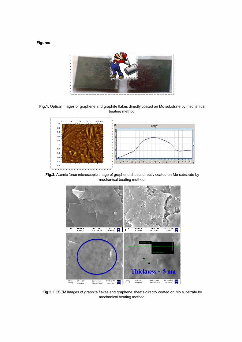
Figures
Fig.1. Optical images of graphene and graphite flakes directly coated on Mo substrate by mechanical
beating method.
Fig.2. Atomic force microscopic image of graphene sheets directly coated on Mo substrate by
mechanical beating method.
Fig.2. FESEM images of graphite flakes and graphene sheets directly coated on Mo substrate by
mechanical beating method.
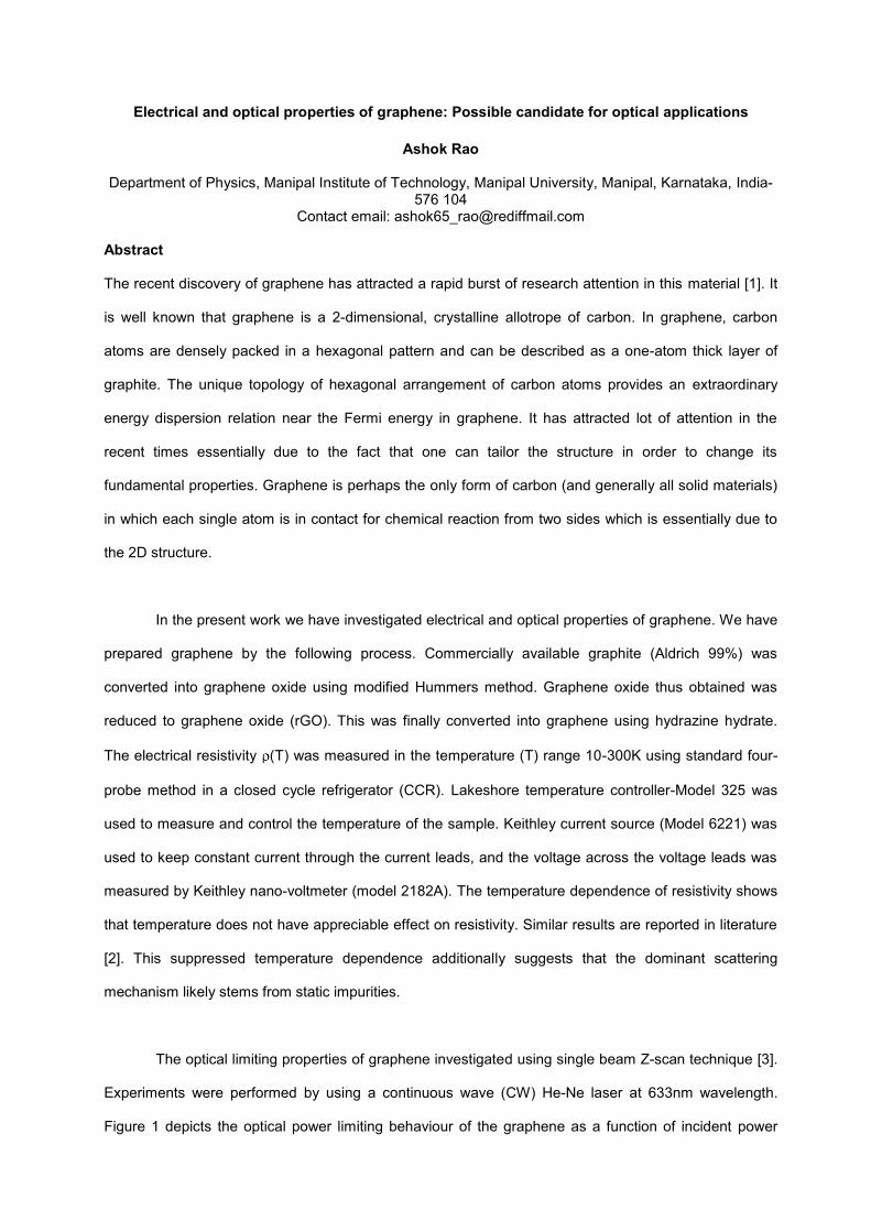
Electrical and optical properties of graphene: Possible candidate for optical applications
Ashok Rao
Department of Physics, Manipal Institute of Technology, Manipal University, Manipal, Karnataka, India-
576 104 Contact email: [email protected]
Abstract The recent discovery of graphene has attracted a rapid burst of research attention in this material [1]. It
is well known that graphene is a 2-dimensional, crystalline allotrope of carbon. In graphene, carbon
atoms are densely packed in a hexagonal pattern and can be described as a one-atom thick layer of
graphite. The unique topology of hexagonal arrangement of carbon atoms provides an extraordinary
energy dispersion relation near the Fermi energy in graphene. It has attracted lot of attention in the
recent times essentially due to the fact that one can tailor the structure in order to change its
fundamental properties. Graphene is perhaps the only form of carbon (and generally all solid materials)
in which each single atom is in contact for chemical reaction from two sides which is essentially due to
the 2D structure.
In the present work we have investigated electrical and optical properties of graphene. We have
prepared graphene by the following process. Commercially available graphite (Aldrich 99%) was
converted into graphene oxide using modified Hummers method. Graphene oxide thus obtained was
reduced to graphene oxide (rGO). This was finally converted into graphene using hydrazine hydrate.
The electrical resistivity (T) was measured in the temperature (T) range 10-300K using standard four-
probe method in a closed cycle refrigerator (CCR). Lakeshore temperature controller-Model 325 was
used to measure and control the temperature of the sample. Keithley current source (Model 6221) was
used to keep constant current through the current leads, and the voltage across the voltage leads was
measured by Keithley nano-voltmeter (model 2182A). The temperature dependence of resistivity shows
that temperature does not have appreciable effect on resistivity. Similar results are reported in literature
[2]. This suppressed temperature dependence additionally suggests that the dominant scattering
mechanism likely stems from static impurities.
The optical limiting properties of graphene investigated using single beam Z-scan technique [3].
Experiments were performed by using a continuous wave (CW) He-Ne laser at 633nm wavelength.
Figure 1 depicts the optical power limiting behaviour of the graphene as a function of incident power
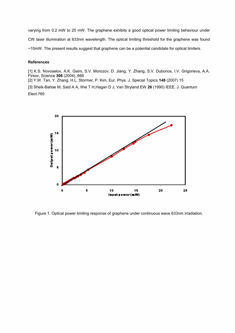
varying from 0.2 mW to 25 mW. The graphene exhibits a good optical power limiting behaviour under
CW laser illumination at 633nm wavelength. The optical limiting threshold for the graphene was found
~10mW. The present results suggest that graphene can be a potential candidate for optical limiters.
References [1] K.S. Novoselov, A.K. Geim, S.V. Morozov, D. Jiang, Y. Zhang, S.V. Dubonos, I.V. Grigorieva, A.A. Firsov, Science 306 (2004), 666 [2] Y.W. Tan, Y. Zhang, H.L. Stormer, P. Kim, Eur. Phys. J. Special Topics 148 (2007) 15
[3] Sheik-Bahae M, Said A A, Wei T H,Hagan D J, Van Stryland EW 26 (1990) IEEE. J. Quantum
Elect.760
Figure 1. Optical power limiting response of graphene under continuous wave 633nm irradiation.
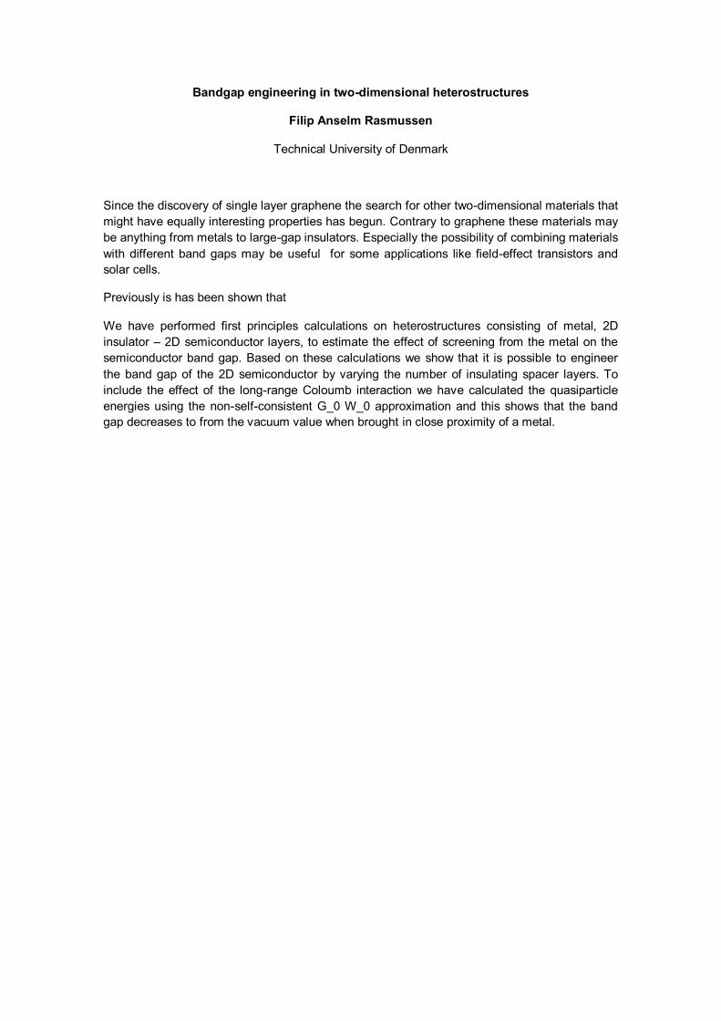
Bandgap engineering in two-dimensional heterostructures
Filip Anselm Rasmussen
Technical University of Denmark
Since the discovery of single layer graphene the search for other two-dimensional materials that
might have equally interesting properties has begun. Contrary to graphene these materials may
be anything from metals to large-gap insulators. Especially the possibility of combining materials
with different band gaps may be useful for some applications like field-effect transistors and
solar cells.
Previously is has been shown that
We have performed first principles calculations on heterostructures consisting of metal, 2D
insulator 2D semiconductor layers, to estimate the effect of screening from the metal on the
semiconductor band gap. Based on these calculations we show that it is possible to engineer
the band gap of the 2D semiconductor by varying the number of insulating spacer layers. To
include the effect of the long-range Coloumb interaction we have calculated the quasiparticle
energies using the non-self-consistent G_0 W_0 approximation and this shows that the band
gap decreases to from the vacuum value when brought in close proximity of a metal.
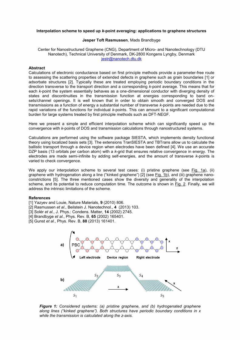
Interpolation scheme to speed up k-point averaging: applications to graphene structures
Jesper Toft Rasmussen, Mads Brandbyge
Center for Nanostructured Graphene (CNG), Department of Micro- and Nanotechnology (DTU Nanotech), Technical University of Denmark, DK-2800 Kongens Lyngby, Denmark
Abstract Calculations of electronic conductance based on first principle methods provide a parameter-free route to assessing the scattering properties of extended defects in graphene such as grain boundaries [1] or adsorbate structures [2]. Typically these are treated employing periodic boundary conditions in the direction transverse to the transport direction and a corresponding k-point average. This means that for each k-point the system essentially behaves as a one-dimensional conductor with diverging density of states and discontinuities in the transmission function at energies corresponding to band on-sets/channel openings. It is well known that in order to obtain smooth and converged DOS and transmissions as a function of energy a substantial number of transverse k-points are needed due to the rapid variations of the functions for individual k-points. This can amount to a significant computational burden for large systems treated by first principle methods such as DFT-NEGF. Here we present a simple and efficient interpolation scheme which can significantly speed up the convergence with k-points of DOS and transmission calculations through nanostructured systems. Calculations are performed using the software package SIESTA, which implements density functional theory using localized basis sets [3]. The extensions TranSIESTA and TBTrans allow us to calculate the ballistic transport through a device region when electrodes have been defined [4]. We use an accurate DZP basis (13 orbitals per carbon atom) with a k-grid that ensures relative convergence in energy. The electrodes are made semi-infinite by adding self-energies, and the amount of transverse k-points is varied to check convergence. We apply our interpolation scheme to several test cases: (i) pristine graphene (see Fig. 1a), (ii)
kinked graphene [2] (see Fig. 1b), and (iii) graphene nano-constrictions [5]. The three mentioned cases show the diversity and generality of the interpolation scheme, and its potential to reduce computation time. The outcome is shown in Fig. 2. Finally, we will address the intrinsic limitations of the scheme. References [1] Yazyev and Louie, Nature Materials, 9 (2010) 806. [2] Rasmussen et al., Beilstein J. Nanotechnol., 4 (2013) 103. [3] Solér et al., J. Phys.: Condens. Matter, 14 (2002) 2745. [4] Brandbyge et al., Phys. Rev. B, 65 (2002) 165401. [5] Gunst et al., Phys. Rev. B, 88 (2013) 161401.
Figure 1: Considered systems: (a) pristine graphene, and (b) hydrogenated graphene along lines ( graphene . Both structures have periodic boundary conditions in x while the transmission is calculated along the z-axis.
a)
b)

Figure 2: (a) Transport through pristine graphene from left (red in Fig. 1a) to right electrode (blue in Fig. 1a) as a function of number of transverse k-points. (b) The interpolated transmission in pristine graphene shows much faster convergence.
b)
a)

Graphene growth on atomically-thin oxidized Cu(111)
Nicolas Reckinger, Eloise Van Hooijdonk, Frédéric Joucken, Anastasia V. Tyurnina, Stéphane Lucas, and Jean-François Colomer
Research Center in Physics of Matter and Radiation (PMR), University of Namur (UNamur), Rue de
Bruxelles 61, B-5000 Namur, Belgium.
The growth of graphene by chemical vapor deposition (CVD) [1] using single-crystal copper has been reported recently [2,3]. The technique holds promise for growing larger graphene domains of higher quality than those obtained from polycrystalline copper (Cu) surfaces (foils or thin films) since the copper substrate is by definition free of grain boundaries and extremely flat. Oriented (111) Cu single crystals offer two additional distinctive advantages: (i) the same hexagonal crystalline symmetry as graphene and (ii) a small lattice mismatch.
In the present work, graphene grown by atmospheric pressure CVD [4] on Cu deposited on basal-plane sapphire is explored by scanning tunneling microscopy (STM) [5]. Two kinds of samples grown under different conditions are investigated: a reference sample revealing an expected hexagonal moiré pattern and a second sample exhibiting an unusual linear moiré pattern.
Based on X-ray diffraction (XRD) and low energy electron diffraction (LEED), the deposited Cu films are confirmed to be (111) oriented. The LEED pattern of the graphene/Cu(111)/sapphire exhibit a diffuse ring indicative of rotational disorder of single-layer graphene domains or/and multi-layer graphene with each layer independently stacked. The moiré pattern of the reference sample appears as a hexagonal superlattice (lattice constant of 2.6 nm) which results both from the misalignment of the hexagonal lattices of the graphene layer and the Cu(111) substrate, and from the mismatch of their lattice constants (2.46 Å and 2.56 Å, respectively). For the second sample, the observed moiré superstructure is composed of well-defined linear periodic modulation with a wavelength of 2.3 nm.
Several hypotheses can be proposed to elucidate these unexpected linear patterns. The first possibility is that the Cu surface might not be oriented along the (111) direction but locally along the (100) direction. However, this can be ruled out by (i) the LEED analysis showing a six-fold symmetry corresponding to the hexagonal Cu(111) surface, and not the four-fold symmetry, expected for a cubic (100) Cu surface; (ii) the maximum period of the linear moiré superstructure of 1.6 nm (< 2.3 nm) in the case of graphene on Cu(100). Another possible explanation is the presence of a thin copper oxide layer on top of the Cu(111) film, as suggested by a weak oxygen peak and a small shift of the Cu peak as observed by Auger electron spectroscopy. This copper oxide can neither be Cu2O(111), since it has a hexagonal symmetry, nor can it be Cu2O(100) because (i) the LEED pattern symmetry does not correspond to the cubic symmetry of Cu2O(100) and (ii) it has been widely reported not to form on Cu(111). Since the previous assumptions prove unsatisfactory to account for the linear moiré patterns, we hypothesize a superposition of graphene over an oxygen-induced reconstruction of Cu(111) (so-
-structure [6]), corroborated by hard-sphere atomic modelling and LEED results.
As a summary, we bring some evidence that, under certain growth conditions, graphene can grow on atomically-thin oxidized copper. References [1] X. Li, W. Cai, J. An, S. Kim, J. Nah, D. Yang, R. Piner, A. Velamakanni, I. Jung, E. Tutuc, S. K. Banerjee, L. Colombo, and R. S. Ruoff, Science 324, 1312 (2009). [2] K. M. Reddy, A. D. Gledhill, C. H. Chen, J. M. Drexler, and N. P. Padture, Appl. Phys. Lett. 98, 113117 (2011). [3] B. S. Hu, H. Ago, Y. Ito, K. Kawahara, M. Tsuji, E. Magome, K. Sumitani, N. Mizuta, K. I. Ikeda, and S. Mizumo, Carbon 50, 57 (2012). [4] I. Vlassiouk, M. Regmi, P. Fulvio, S. Dai, P. Datskos, G. Eres, and S. Smirnov, ACS Nano 5, 6069 (2011). [5] N. Reckinger, E. Van Hooijdonk, F. Joucken, A. Tyurnina, S. Lucas, and J.-F. Colomer, Nano Res. 4, 154 (2014). [6] T. Matsumoto, R. A. Bennett, P. Stone, T. Yamada, K. Domen, and M. Bowker, Surf. Sci. 471, 225 (2001).

Figure 1: (a) XRD and (b) LEED patterns recorded at E = 100 eV of the as-deposited Cu(111)/sapphire substrate. (c) LEED pattern of the graphene/Cu(111)/sapphire substrate recorded at E = 75 eV.
Figure 2: (a) Experimental STM image displaying the experimental hexagonal moiré superstructure and (b) the corresponding hard-sphere atomic model, with a deduced 6° rotation angle between graphene
and Cu(111) to match the spacing of 1.98 nm. (c) Experimental STM image displaying the experimental linear moiré pattern and (d) the corresponding hard-sphere atomic model, with a deduced 50° rotation
angle between graphene and Cu(111) to match the linear spacing of 2.3 nm.
(c)
(c) (d)
(a) (b)
Figure 3: -structure (obtained from [6]); (b) and (c) progressively simplified calculated LEED pattern to account for the experimental pattern shown in (d) (E
= 51.1 eV).

Controlled synthesis and properties at the nano-scale of highly reduced
graphene oxide (HRGO) obtained by Langmuir-Blodgett method.
F.G Requejoa, F.C. Herrera
a, P.C. dos Santos Claro
a, J.M. Ramallo López
a, G. Morales
b, G. Lacconic
c,
R.D. Sanchezd, J. Lohr
d, J. Avila
eand M. Asensio
e
a) INIFTA (CONICET-UNLP), 1900 La Plata, Argentina.b) Universidad Nacional de Río Cuarto. Río Cuarto, Argentina.
c) INFIQC, Fc. Cs. Químicas, UNC. Córdoba. Argentina.c) Centro Atómico Bariloche and Instituto Balseiro, CNEA. S.C. de Bariloche (RN), Argentina.
d) Synchrotron SOLEIL, Saint Aubin-BP 48, 91192 Gif sur Yvette Cedex, France.
Contact@E-mail [email protected]
We present here the controlled obtaining of highly reduced graphene oxide (HRGO) thin films by using of Langmuir-Blodgett (LB) technique. To have a deep and definitive information about the chemical species in the samples and the spatial distribution of them, a multiple characterization on the different stages of the material (i.e. before and after each reduction treatment) was performed employing both spectroscopic and image-based analysis ones such as: SEM, AFM, grazing XRD, RAMAN, XPS and their space-solved versions: micro-RAMAN and nano-XPS. Finally, in order to correlate the chemical state, structure and defects present in the HRGO thin films, a set of current-voltage curves onmacroscopic and microscopic distance between electrodes.
Graphene oxide was obtained by Hummers’ method [1] and deposited on Si(100) by LBtechnique. Similar samples could be obtained just by simply setting of the same parameters at the LB setup. Different thermal reduction treatments were performed subsequently at different accumulative steps at 300, 600 and 700 °C under UHV conditions. After each thermal treatment samples werecharacterized. Grazing XRD experiments were performed at the DRX2 beamline at the LNLS Synchrotron Laboratory (Campinas, Brazil), XPS and nano-XPS analysis were performed at the ANTARES beamline [2] at the SOLEIL Synchrotron Laboratory (Saint Aubin, France). The microscopic determinations of current-voltage curves were achieve using the assistance of a nanomanipulator and a probe station.
The thickness of the samples was analyzed by AFM and grazing XRD. It results thinner afterthermal treatments, reaching between 1.3 and 1.8 nm after reduction treatments at 600 °C, which is very close to the expected value for very few layers HRGO [3]. After thermal treatments we also observe, from RAMAN experiments, the decrement of D band, associated with defective centers. Similar information was obtained by XPS, were different O-species were eliminated after each thermal treatment. From micro-RAMAN and nano-XPS we can establish the high spatial homogeneity of the thin-film after reduction treatments. In summary we can show a simple procedure to obtain, with high reproducibility, almost monolayers of HRGO with extreme chemical and structural homogeneity and conductive properties.
a)
b)
Figure: a) SEM image after thermal treatment at 600 ºC; b) high resolution XPS spectra of the C 1s peak of GO samples after different thermal treatments for reduction.
References[1] W.S. Hummers Jr., R.E. Offeman, J. Am. Chem. Soc. 80 (1958) 1339.[2] J. Avila, I. Razado-Colambo, S. Lorcy, J-L. Giorgetta, F. Polack and M.C. Asensio, Journal of Physics: Conference Series 425 (2013) 132013.[3] S. Dubin, S. Gilje K. Wang, V.C. Tung, K. Cha, A.S. Hall, J. Farrar, R. Varshneya, Y.Yang and R.B. Kaner, ACS Nano, 4 (2010) 3845.
292 291 290 289 288 287 286 285 284 283
Counts
/ a
rb.u
nits
Binding Energy / eV
As prepared treated at 300 ºC in UHV treated at 600 ºC in UHV pristine graphene
Raman spectroscopy in bilayer graphene samples with many different twisting angles
H. B. Ribeiro1, K. Sato3, G. S. N. Eliel2, E. A. T. de Souza1, Po-Wen Chiu4, R. Saito3, and M. A. Pimenta2
1MackGraphe, Mackenzie Presbyterian University, R. da Consolação 896, São Paulo, Brazil 2Physics Department, UFMG, Av. Antônio Carlos, 6627, Belo Horizonte, Brazil
3Department of Physics, Tohoku University and CREST, Sendai, 980-8578, Japan 4Department of Electrical Engineering, National Tsing Hua University, Hsinchu 300, Taiwan
Abstract
In this work, we performed a Raman spectroscopy study of bilayer graphene samples with many
different twisting angles, using three different laser lines in the visible range. By controlling the growth
parameters in the CVD method, it was possible to obtain twisted bilayer graphene samples where both
the bottom and top layers exhibit a hexagonal morphology. Therefore, the rotation angles between the
two layers were determined by a simple optical analysis for more than 150 samples, as shown in Fig 1.
Raman mapping of the 150 samples were obtained using the 488 nm, 532nm and 633 nm laser lines,
and the intensities and FWHM of all Raman features, mainly the G and 2D bands, were analyzed as
function of the twisting angle. A huge increase in the G band intensity could be observed for samples
with intermediate twisting angles (between 9 and 14 degrees) and the results could be explained in
terms of resonances with van Hove singularities [1] that arise from the coupling between the two Dirac
cones of the bottom and top layers. For low and large twisting angles, we have observed that the ratio
between the G band intensities in the bilayer and single layer regions (IB/IS) depends on the laser
energy and also exhibit different dependence for low and large twisting angles. We have also analyzed
the 2D band shape and intensity as a function of the twisting angle and our results reveals that the Dirac
cones of the two layers are coupled for low twisting angles and practically uncoupled for large twisting
angles.
Our analysis always allowed us to obtain the twisting angle dependence of the G band FWHM that can
be correlated with the G band enhancement due to resonances with van Hove singularities. We will also
present results of a number of sharp and extra peaks just above and below the G band position, which
are ascribed to the umklapp double resonance process, where the momentum conservation is provided
by the wavevector connecting the two Dirac cones of the bottom and top graphene layers.
References
[1] K. Sato, R. Saito, C. Cong, Ting Yu, and Mildred S. Dresselhaus, Phys. Rev. B, 86 (2012) 125414.
Figures
Fig. 1 – Optical image of sample showing the bilayer graphene and the rotation angle between two layers.

Nanoscale Chemical & Physical imaging of Graphene and other carbon species with nanoRaman
E. Leroy
1, R. Lewandowska
1, O. Lancry
1, J. Schreiber
1, A Krayev
2, S Saunin
2
HORIBA Scientific1, Avenue de la Vauve, Passage Jobin Yvon CS 45002, 91120 Palaiseau, France
AIST-NT inc.2 359 Bel Marin Keys Blvd, suite 20, Novato, CA 94949, USA
Contact: [email protected]
Graphene is a strong Raman scatterer and this technique has long been used to determine quality and number of layers of such material; however it lacks the spatial resolution that is necessary to study engineered structures in detail. Scanning Probe Microscopy (SPM), and especially Atomic Force Microscopy (AFM) is a powerful technique to image physical properties of graphene, such as topography, conductivity or other electrical properties. Combining both techniques is challenging but extremely powerful, as it makes imaging of both chemical and physical properties possible, although conventional Raman only provides limited spatial resolution. The step beyond co-localized AFM and Raman is nanoRaman or nano-spectroscopy in general.
In this talk, we will present the latest development in terms of Tip Enhanced Raman spectroscopy (TERS) that make possible nanoscale imaging of chemical and physical properties of graphene and other carbon species: innovative integration of technologies brings high-throughput optics and high-resolution scanning for high-speed imaging without interferences between the techniques. The latest developments in near-field optical probes now provide reliable solutions for academic and industrial researchers alike to easily get started with nanoscale spectroscopy.
TERS (nanoRaman) image of graphene oxide and carbon nanotubes showing 15nm resolution

Rapid Graphene Fabrication and Ultrafast Characterization
J. Riikonen, C. Li, W. Kim, J. Susoma, A. Säynätjoki, L. Karvonen, and H. Lipsanen
Aalto University, Department of Micro- and Nanosciences,Micronova, Tietotie 3, FI-02150 Espoo, Finland
Chemical vapour deposition (CVD) of graphene on copper is a widely studied method for manufacturing monolayer graphene on large-area substrates. As for any emerging material, cost-efficiency is one of the key factors on the road to industrial scale fabrication. Minimizing processing time is obviously one the essential parameters. The optimization of the whole fabrication process includes also characterization methods suitable for high throughput.
We demonstrate ultrafast characterization of graphene by simultaneous third-harmonic and photoluminescence microscopy. In addition, we present rapid synthesis of monolayer graphene on copper. Utilizing photo-thermal CVD, uniform high-quality graphene films covering the whole copper surface can be fabricated only in about 30 s (~11 mbar). In addition, the total processing time can be significantly reduced due fast ramp rates enabled by minimized thermal mass. Cold wall chamberminimizes contamination originating from the sidewalls, which is one critical factor in fabricating monolayer material. Cold wall facilitates also real-time temperature control by enabling utilization of pyrometer in temperature detection. -Raman mapping and electrical measurements including various devices were used to confirm the graphene quality. Raman spectroscopy showed clear evidence of high-quality monolayer graphene as we observed an average 2D/G > 3 with very low defect density (D/G ratio) using an area of
2. Field-effect mobility determined using constant mobility
model was 3000 cm2/Vs [1]. We expect that these results will partly pave the way toward cost-efficient
graphene fabrication.
In addition to typical global back gate utilized graphene field-effect transistors (GFET), we have also fabricated highly tunable local top and bottom gate controlled complementary graphene devices [2].Both top and bottom gate oxides (Al2O3) were grown using atomic layer deposition (ALD). In the CMOS-like configuration, two transistors are individually controlled by electrostatic doping. This complementary structure along with the field-effect control over the graphene channel enables switchable operationbetween inverter (p n FETs) and voltage controlled resistor (n p FETs). Moreover, our approach enables variety of different substrates including non-conductive ones.
Finally we introduce alternative methodology for graphene analysis by presenting ultrafast characterization capabilities of simultaneous third-harmonic and fluorescence microscopy [3]. Without optimization of the homemade tool, imaging is for example orders of magnitude faster than inconventional Raman mapping (an area of hundreds of micrometers squared was imaged only in few seconds). The multiphoton microscopy produces images with high contrast in third harmonic generation(THG) between monolayer graphene compared to the substrate. While different monolayer samples produce constant THG signal, bilayer can be clearly distinguished from monolayer. Furthermore, the THG signal increases with the number of graphene layers to a threshold thickness until the signal starts to decrease.
References
[1] Riikonen, J.; Kim, W.; Li, C.; Svensk, O.; Arpiainen, S.; Kainlauri, M.; Lipsanen, H., Carbon, 62
(2013) 43-50.[2] Kim, W.; Riikonen, J.; Li, C.; Chen, Y.; Lipsanen, H., Nanotechnology, 24 (2013) 395202-1-5.[3] Saynatjoki, A.; Karvonen, L.; Riikonen, L.; Kim, W.; Mehravar, s.; Norwood, R.A.; Peyghambarian, N.; Lipsanen, H.; Khanh K., ACS Nano, 7 (2013) 8441-8446.

Graphene-based piezoresistive strain sensors obtained via spray deposition technique
A. Rinaldi, A. Tamburrano, G. De Bellis, F. Marra, M.S. Sarto
CNIS - Sapienza University of Rome, via Eudossiana 18, Rome, Italy [email protected]
Abstract The piezoresistive effect is often used in sensing applications, requiring the measurement of strain. Since the development of piezoresistive materials for strain measurement by Mason et al.[1], several efforts have been concentrated on fabricating piezoresistive strain sensors with high gauge factor and high cut-off frequency. During the last decade a new kind of strain sensors made of nanocomposites has been developed [2][3]. Very recently, innovative graphene-based nanocomposite strain sensors have been fabricated for structural health monitoring applications [4]. These sensors are characterized by a high gauge factor up to 2% strain, cut off frequency up to 50-100 kHz depending on their size, but limited sensitivity for small strain due to the polymeric matrix [4]. To overcome such limitation, sensing coating made via spray casting technique can be developed [5]. The work presented here is part of a larger study whose goal is to realize a sensing coating for structural health monitoring. The proposed sensor consists of a graphene-based film, obtained through the deposition of a colloidal suspension of Graphene Nanoplatelets (GNPs) over the substrate to be monitored. GNPs are produced by liquid exfoliation of thermally expanded Graphite Intercalation Compound (GIC) (commercially available Grafguard 160-50N), as reported in [6]. After thermal expansion of GIC at 1150°C for 5 s, the resulting Wormlike Expanded Graphite (WEG) is dispersed in 1-propanol, and the resulting mixture is tip sonicated using an ultrasonic processor, thus obtaining GNPs (Fig. 1). The sonication process is carried out with a pulsed cycle under thermally controlled conditions. The selection of 1-propanol as WEG solvent was inspired by the consideration that 1-proponol is a volatile alcohol with a low boiling point (97 °C) and more environmentally friendly than the usual WEG solvent, such as N,N-Dimethylformamide (DMF) and N-Methyl-2-pyrrolidone (NMP), used in [6]. According to Hansen theory, each materials or solvents is characterized by three Hansen Solubility Parameters (HSPs), representative respectively of the d r) and hydrogen H) bondings. The sum of the square of the previous terms give the square of the Hildebrand
t). In [7], it is reported that good solvents for graph t close to the Hildebrand solubility parameter of graphene ( 23 MPa1/2) and by HSPs d 18 MPa1/2, p 9.3
MPa1/2, H 7.7 MPa1/2. 1-propanol is characterized by t 24.6 MPa1/2, d 16 MPa1/2, p 6.8 MPa1/2, H
17.4 MPa1/2t is coherent with Coleman observation in [8 p H is
within the magic range individuated in [9] for the choice of good solvents for highly reduced graphene oxide. Spray deposition allows a very easy, fast and uniform deposition over a large area. In case of strain sensors having dimensions of 1 cm2, in order to minimize suspension dispersion and to increase the spraying efficiency, GNP concentration should be optimized. Therefore, we investigated the stability of several suspension having different concentrations in the range from 0.05 mg/ml to 0.5 mg/ml. The highest concentration that after three weeks does not show a visible sedimentation with no visible agglomerates is the suspension with a MLG concentration of 0.1 mg/ml. Temperature control of the substrate is a key parameter in order to avoid droplets coalescence before drying; for this reason the deposition process is performed in a chamber with controlled temperature. The selected suspension is then deposited over a polycarbonate beam having silver contact pads and a detachable mask in order to allows GNPs deposition only over the selected area. The piezoresistive effect results from three contributions: the change of the tunneling resistance, the contact resistance between adjacent GNPs, the modification of the number of percolation conduits [10]. The produced GNP films have an average thickness of 10-30 µm. Electromechanical tests, carried out according to ASTM D70-03 and ASTM E251-92 standards, show a quasi-linear increase of the sensor electrical resistance with strain (Fig.2(a)) and a hysteretic behavior (Fig.2(b)) that disappears after 18 mechanical cycles. The reason behind such behavior is investigated through electron microscopy performed at CNIS, using a Zeiss Auriga FESEM. It is observed that before mechanical testing the film surface is rough (Fig.3(a), due to the random distribution of the GNPs resulting from the spray deposition. After a certain number of mechanical stabilization cycles, the film surface becomes smoother due to an alignment of the GNPs along the substrate surface (Fig.3(b)). GNPs reorganization is a direct consequence of the mechanical stabilization. As shown in Fig.(4), the measured gauge factor of the new sensor ranges from 14 to 80 for strains below 0.2%. Moreover, their cut off-frequency is limited only by the substrate characteristics. These sensors show

their best performances for very small strain, typically from 1 to 2000 microstrain (as depicted in the inset of Fig.4), because for larger strain the GNPs film begins to deteriorate. References [1] W.P. Mason, R.N. Thurston, Journal of the Acoustical Society of America. 29 (1957) 1096 1101 [2] C. Xing; Z. Xiaohu, K. Ji-Kwan, L Xinxin, D. Lee, Journal of Vacuum Science & Technology B:
Microelectronics and Nanometer Structures 6 (2011) [3] G. Yin, N. Hu, Y. Karube, Y. Li, H. Fukunaga, Journal of composite materials 45(12) 1315-1323 [4] A. Tamburrano, F. Sarasini, G. De Bellis, A. D'Aloia, M. S. Sarto, Nanotechnology. 24(2013), 465702. [5] J.F.Capsal, C. David, E. Dantras, C. Lacabanne, Smart Materials and Structures, 21 (2012) 1-7 [6] G De Bellis, A Tamburrano, A Dinescu, ML Santarelli, and MS Sarto. Carbon 49 (2011):4291 4300 [7] E.Y. Choi, W.S. Choi, Y.B. Lee, Y. Y.N, Nanotechnology 22 (2011) [8] Y. Hernandez, M. Lotya, D. Rickard, S.D. Bergin, J.Coleman,Langumir 26 (2010) 3208-3213 [9] S. Park, J.An, I.Jung, R.D.Piner, S.J.An, X.Li, A.Velamakani, R.S. Ruoff, Nanoletters 9 (2009), 1593-
1597 [10] , IEEE NANO 2011, Aug. 15-19 2011, Portland,
(OR). Figures
(a)
(b)
Fig.1 SEM of a GNP flake. Fig. 2 Sensor resistance versus strain measured at the first mechanical cycle (a) and sensor resistance variation during mechanical stabilization tests (b).
(a)
(b)
Fig.3 SEM images of the GNP film as deposited (a) and after mechanical stabilization (25 cycles) (b).
Fig.4 Gauge factor versus strain after mechanical stabilization (25 cycles).
2 m
400nm 0 5 10 15 20160
180
200
220
240
Strain
Resis
tance [
K
]
x 10-4
0 40 80 120140
160
180
200
220
240
Time [s]
Resis
tance [
K]
mechanical conditionig of the sensor
2 m 2 m
0 5 10 15 200
20
40
60
80
Strain
Gauge f
acto
r
x 10-4
10-4
10-3
10-2
14
18
22
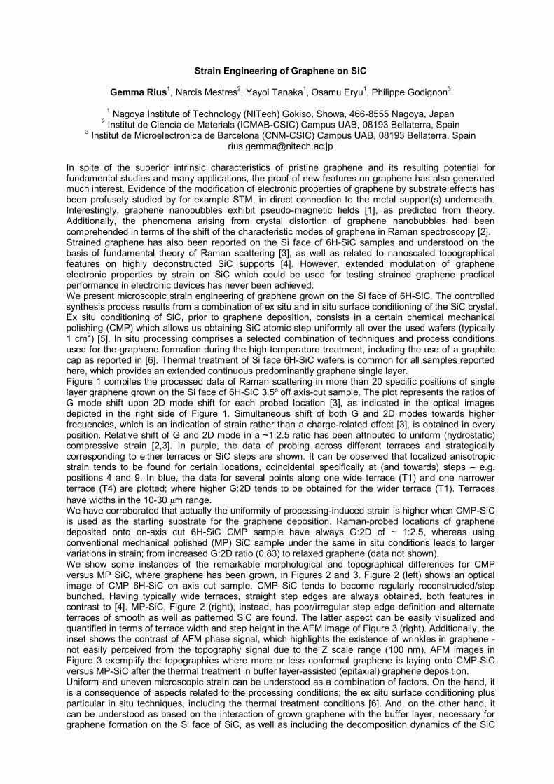
Strain Engineering of Graphene on SiC
Gemma Rius1, Narcis Mestres
2, Yayoi Tanaka
1, Osamu Eryu
1, Philippe Godignon
3
1 Nagoya Institute of Technology (NITech) Gokiso, Showa, 466-8555 Nagoya, Japan
2 Institut de Ciencia de Materials (ICMAB-CSIC) Campus UAB, 08193 Bellaterra, Spain
3 Institut de Microelectronica de Barcelona (CNM-CSIC) Campus UAB, 08193 Bellaterra, Spain
In spite of the superior intrinsic characteristics of pristine graphene and its resulting potential for fundamental studies and many applications, the proof of new features on graphene has also generated much interest. Evidence of the modification of electronic properties of graphene by substrate effects has been profusely studied by for example STM, in direct connection to the metal support(s) underneath. Interestingly, graphene nanobubbles exhibit pseudo-magnetic fields [1], as predicted from theory. Additionally, the phenomena arising from crystal distortion of graphene nanobubbles had been comprehended in terms of the shift of the characteristic modes of graphene in Raman spectroscopy [2]. Strained graphene has also been reported on the Si face of 6H-SiC samples and understood on the basis of fundamental theory of Raman scattering [3], as well as related to nanoscaled topographical features on highly deconstructed SiC supports [4]. However, extended modulation of graphene electronic properties by strain on SiC which could be used for testing strained graphene practical performance in electronic devices has never been achieved. We present microscopic strain engineering of graphene grown on the Si face of 6H-SiC. The controlled synthesis process results from a combination of ex situ and in situ surface conditioning of the SiC crystal. Ex situ conditioning of SiC, prior to graphene deposition, consists in a certain chemical mechanical polishing (CMP) which allows us obtaining SiC atomic step uniformly all over the used wafers (typically 1 cm
2) [5]. In situ processing comprises a selected combination of techniques and process conditions
used for the graphene formation during the high temperature treatment, including the use of a graphite cap as reported in [6]. Thermal treatment of Si face 6H-SiC wafers is common for all samples reported here, which provides an extended continuous predominantly graphene single layer. Figure 1 compiles the processed data of Raman scattering in more than 20 specific positions of single layer graphene grown on the Si face of 6H-SiC 3.5º off axis-cut sample. The plot represents the ratios of G mode shift upon 2D mode shift for each probed location [3], as indicated in the optical images depicted in the right side of Figure 1. Simultaneous shift of both G and 2D modes towards higher frecuencies, which is an indication of strain rather than a charge-related effect [3], is obtained in every position. Relative shift of G and 2D mode in a ~1:2.5 ratio has been attributed to uniform (hydrostatic) compressive strain [2,3]. In purple, the data of probing across different terraces and strategically corresponding to either terraces or SiC steps are shown. It can be observed that localized anisotropic strain tends to be found for certain locations, coincidental specifically at (and towards) steps e.g. positions 4 and 9. In blue, the data for several points along one wide terrace (T1) and one narrower terrace (T4) are plotted; where higher G:2D tends to be obtained for the wider terrace (T1). Terraces
have widths in the 10-30 m range. We have corroborated that actually the uniformity of processing-induced strain is higher when CMP-SiC is used as the starting substrate for the graphene deposition. Raman-probed locations of graphene deposited onto on-axis cut 6H-SiC CMP sample have always G:2D of ~ 1:2.5, whereas using conventional mechanical polished (MP) SiC sample under the same in situ conditions leads to larger variations in strain; from increased G:2D ratio (0.83) to relaxed graphene (data not shown). We show some instances of the remarkable morphological and topographical differences for CMP versus MP SiC, where graphene has been grown, in Figures 2 and 3. Figure 2 (left) shows an optical image of CMP 6H-SiC on axis cut sample. CMP SiC tends to become regularly reconstructed/step bunched. Having typically wide terraces, straight step edges are always obtained, both features in contrast to [4]. MP-SiC, Figure 2 (right), instead, has poor/irregular step edge definition and alternate terraces of smooth as well as patterned SiC are found. The latter aspect can be easily visualized and quantified in terms of terrace width and step height in the AFM image of Figure 3 (right). Additionally, the inset shows the contrast of AFM phase signal, which highlights the existence of wrinkles in graphene - not easily perceived from the topography signal due to the Z scale range (100 nm). AFM images in Figure 3 exemplify the topographies where more or less conformal graphene is laying onto CMP-SiC versus MP-SiC after the thermal treatment in buffer layer-assisted (epitaxial) graphene deposition. Uniform and uneven microscopic strain can be understood as a combination of factors. On the hand, it is a consequence of aspects related to the processing conditions; the ex situ surface conditioning plus particular in situ techniques, including the thermal treatment conditions [6]. And, on the other hand, it can be understood as based on the interaction of grown graphene with the buffer layer, necessary for graphene formation on the Si face of SiC, as well as including the decomposition dynamics of the SiC
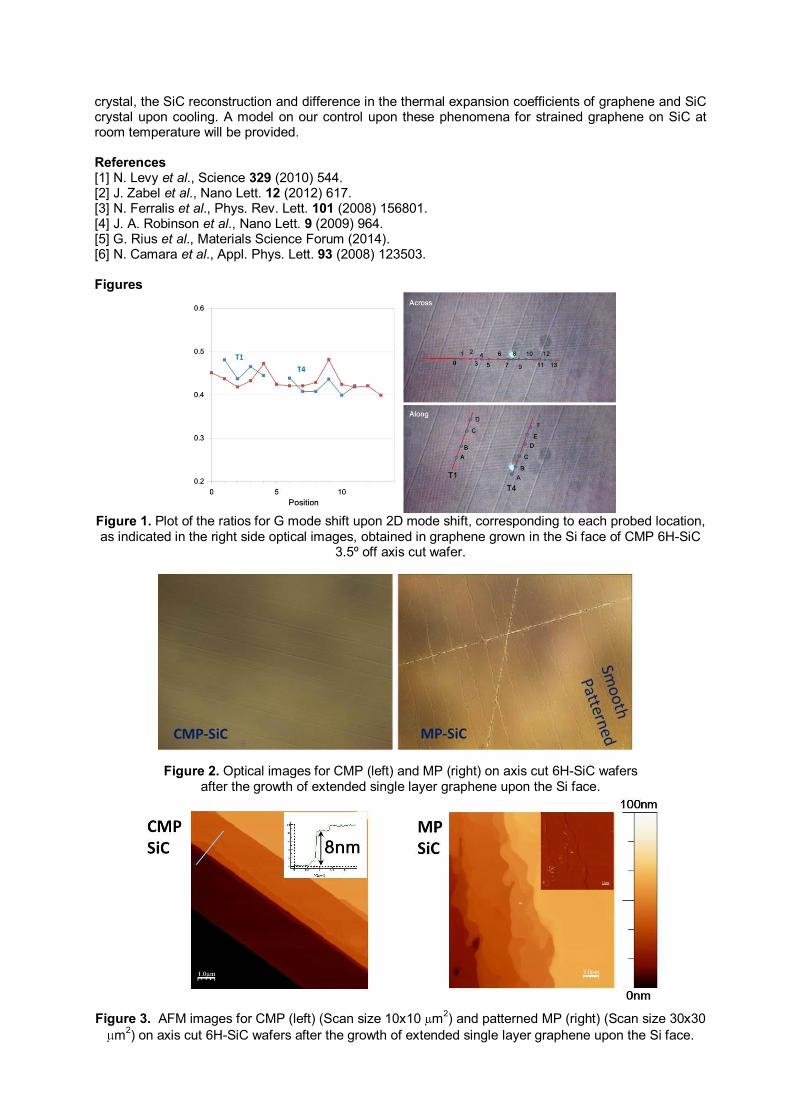
crystal, the SiC reconstruction and difference in the thermal expansion coefficients of graphene and SiC crystal upon cooling. A model on our control upon these phenomena for strained graphene on SiC at room temperature will be provided. References [1] N. Levy et al., Science 329 (2010) 544. [2] J. Zabel et al., Nano Lett. 12 (2012) 617. [3] N. Ferralis et al., Phys. Rev. Lett. 101 (2008) 156801. [4] J. A. Robinson et al., Nano Lett. 9 (2009) 964. [5] G. Rius et al., Materials Science Forum (2014). [6] N. Camara et al., Appl. Phys. Lett. 93 (2008) 123503. Figures
Figure 1. Plot of the ratios for G mode shift upon 2D mode shift, corresponding to each probed location, as indicated in the right side optical images, obtained in graphene grown in the Si face of CMP 6H-SiC
3.5º off axis cut wafer.
Figure 2. Optical images for CMP (left) and MP (right) on axis cut 6H-SiC wafers
after the growth of extended single layer graphene upon the Si face.
Figure 3. AFM images for CMP (left) (Scan size 10x10 m
2) and patterned MP (right) (Scan size 30x30
m2) on axis cut 6H-SiC wafers after the growth of extended single layer graphene upon the Si face.

�������������� ����������������������������������������������
������������������������ ������������������ ����������������� ��������������� �������������� �������������������������������� ����������!��"���������������"���������������������
���� �
#��$�%!���&����'����"����� ( �)( �*�&�����!��+#�#�$�%!$���,$������"����+��'���������*���- ���&��������!��+#
�#�.���#�/�!�/�������,������������0��'�����+�/�&������������&��������1���- ���&��������!��+�����2"#���#���#��
�������3��� ���� /� /�4%�+��� ��������� 56��7� ������� ��� /���� ������������ �� ����'�� ����� �� 53�,7� �������� �� "��� /�� ����� /��� ���� ���� ��8������� ����� ������������ ���������� �� � /�� +�� ��������� ���������"����� ���������� �/�9�"����"�������#�3����:�� �/��������� ���+� ��������/���3�,� /������������4����� �������+��� ��/������9� �������� ��� !� ���� 3��� �9� �� 5!3�7�� �% �� � ;���� ����� 6% �� � 3��� �9� �� 563�7#� 3��� ���� /� ��������������/��������������������������������/������/�"��������/�/�9�"�� �'��������������������#�!3��������� ��� "������ �� � ���� +� ���� �� �/���� "�� ����� �� ����� ��� ��� �������"�� /�� /�9�"�� ���������������������< =#����'��������3�,���������������/������������+�������/��������������� ����+������������������ �����'���������������������������������/����4����4������� ������//����'���+���#!�� ���� ����� /� ������ ��� �� "��� � �� � ���������� ���� ����� ���� /�"�������� ��8������ ���������������������������� ((>��<�=#�?����!3���������� ���� ���"'��*((>�������6���������������9����� �������� ���� ��8���������� ��� ������ /� �����������+�� �� ����'��+� <�%-=� �� � ����������� �� ����� �������"� ������������#����� ������� �� �%��.� ��4�� 6��� ����� ������� 5���� 6������ 7�� "��� �����/���� � �� 8������ �� � �� �//������ :�� � /� /�9�"�� ������������ ��"��������� ��4� �� ������ ����������� /� �"��� -((� ��@�8� /��������������������� �*)�A#����������������������������)((% ((>������������/��� �"������'�������� ��������������������6������������8��������'� ��������������������������������������������"���/������������������ ((�>�#����'���� ��������/�� �����/� ������4�����������������4������� ����� ��������� �� ���� �����/���������� �� /�������� ��"�������� ��� ����"�� �� ��'� �� ���� �����"�� ����� /� ��+����� �� � ������������������/�����/�����������'��������������4����������� ���+�������'����� �'����#�3��� ������� ���%��BC����� 5����6������ �7����� ��� �%"��� � ���� ���� �� � +�%��������� � ���� ����5����6�������7��/�"������ ������������3�,�/�������������4��"�������� #��3�����D�������������������������������� ���'���/�����������������������������/����������%/%���%����4��������/���� ����������4���� �������� �� ���� �� � !3�� ������#� !�� � ��� �� � ����� ����� ������� �� � 6��� ������� <E=� 4�� "����� �� ����3�,#
�
���������
< =��#�#�.����������#������$�����5�( (7��1E-#<�=��#��F��������#�����#���+�#�����#�����5�( �7�(��-(G#�<�=�6#�&�����������#��$����������������5�( (7�E #�<)=��#�H�����#��$��������+����5�( �7� �(( #�<-=��#�&�4�� ������#��$�����������5�( �7����#�<E=��#&�������#��$������$��������+���5�( (7�-G)#

��� ���
��� �� � % H� ��������������� �� �� �� #- ��������� / �%��BC ��� ��� ��� ����������� ����������� 3�,#� 3��� ���� /� ���� ��/������� �'���� ���� ��� ���� � #� !�����B� �:����� /� ���� ���������� �� �������� ��:�� � �� ������ �� ������ ������# 3�� ��� ���� �8���� �� ������ ����������'��� �"+���������
��� ����%�3,��������/���������������"����#�3������������������'�������4����������� ���'��������������/�������� ����"��/��#�5�����7�.�����/���/ � �� �����������+��������#�
��� �� ��I��:���� / � .+� ��������� ��� �� 4��� �������� 3�,

The nanoscale effects of resistive switching in graphene oxide thin films
M. Rogala1,2
, P.J. Kowalczyk1, W. Kozlowski
1, A. Busiakiewicz
1, I. Wlasny
1, S. Pawlowski
1, G. Dobinski
1,
M. Smolny1, L. Lipinska
3, R. Kozinski
3, K. Librant
3, P. Dabrowski
3, J.M. Baranowski
3, K. Szot
2, Z. Klusek
1
1 Department of Solid State Physics, Faculty of Physics and Applied Informatics, University of Lodz,
Pomorska 149/153, 90-236 Lodz, Poland
2 Peter Grünberg Institut & JARA-FIT, Forschungszentrum Jülich, 52425 Jülich, Germany
3 Institute of Electronic Materials Technology, Wolczynska 133, 01-919 Warsaw, Poland
Resistive switching (RS) processes, investigated previously mainly in metal oxides [1], showed a new way of non-volatile data storage in solid state devices. The principles of operation of novel resistive random-access memory (ReRAM) consist of electrically inducted reversible changes of material resistivity between well distinguishable low resistance (ON) and high resistance (OFF) states. The RS is closely related to the memristance according to "memory resistor" (memristor) which is a passive two terminal electrical component predicted theoretically by Leon Chua in the seventies of the last century [2].
It was shown that resistive switching occurs also in graphene oxide (GO) [3]. The RS observed in GO seems nowadays to be highly perspective in modern electronic applications mainly because it gives the possibility of using GO as data storage in transparent and flexible devices. However, the exact processes that are behind RS phenomena in GO or that accompany it are up to date not fully recognized.
We will discuss the conditions which must be met in order to achieve the effect of changes of resistance in GO. In our experiments we used graphene oxide produced using modified Hummers method. The GO thin films of various thicknesses (20 100 nm) were spin-coated on a silicon substrate covered with platinum, which was the flat bottom electrode. The top electrode, which was in contact with GO film, was the Pt covered tip of atomic force microscope (AFM). Environmentally controlled AFM setup was used, which allows for investigations in vacuum, different gases and control of humidity in the range of up to 70%RH. The use of inert electrode material in combination with very low contact area of the top electrode allows us to analyse the influence of the environmental factors on resistive switching processes occurring in GO.
By the use of atomic force microscope we were able to modify the electrical conductivity in nano-regions of GO thin film between ON and OFF states, which is schematically shown on the figure 1. The observed resistive switching has bipolar character (as presented in the figure 2), which is related to the asymmetry of the experimental setup (top of the sample is exposed to the environment which can be controlled during the experiment). We will present how the composition of the atmosphere around GO influences the strength of the RS effect. We will also focus on the dependence between the effectiveness of the electrical modification of the material and the thickness of GO film. We will discuss observed reduction/oxidation processes occurring in graphene oxide layer in terms of its spatial distribution and their consequences on the morphology changes of the thin film. Results of our investigations have a direct connection to the challenges the industry will face when GO will be used to construct ReRAM devices with the desired parameters.
This work is supported by the National Science Centre under project DEC-2012/05/B/ST5/00354. References [1] K. Szot, M. Rogala, W. Speier, Z. Klusek, A. Besmehn, R. Waser, Nanotechnology 22 (2011) 254001. [2] D.B. Strukov, G.S. Snider, D.R. Stewart, R.S. Williams, Nature 453 (2008) 80. [3] C.L. He et al., Appl. Phys. Lett. 95 (2009) 232101.

Figures:
1. The schematic presentation of RS in nano-scale on the surface of thin GO film. The local conductivity images were measured by atomic force microscope, which was also used to transform resistance between ON and OFF states.
2. The I(V) curve measured during RS process. The data presents the changes between states of low and high resistance (ON and OFF states), which take place for opposite polarities, meaning the observed RS has bipolar character.
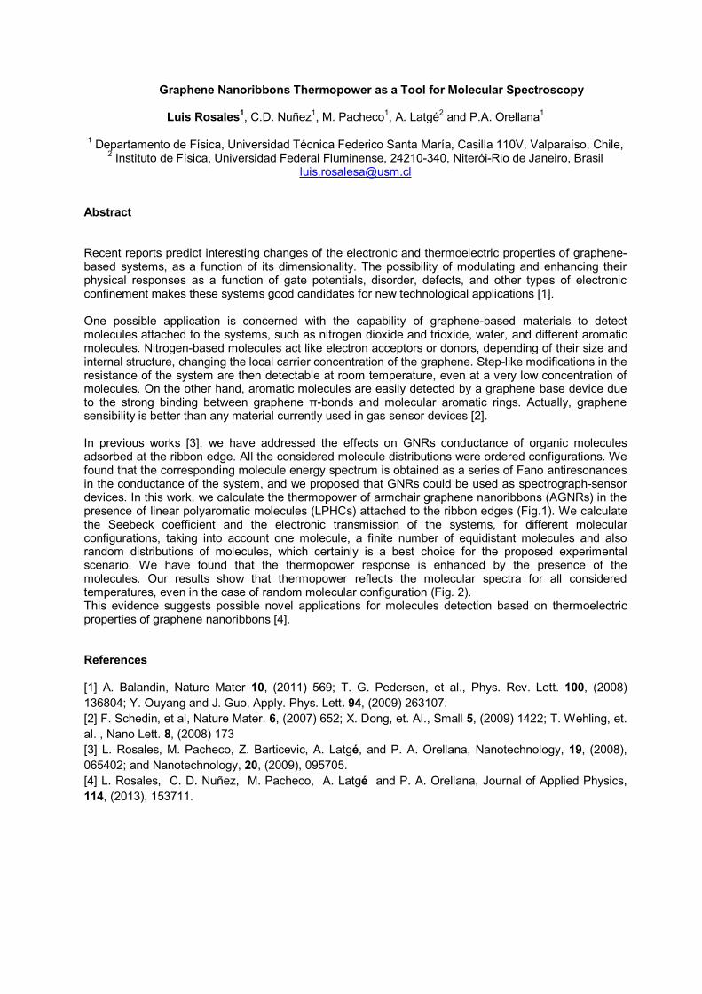
Graphene Nanoribbons Thermopower as a Tool for Molecular Spectroscopy
Luis Rosales1, C.D. Nuñez
1, M. Pacheco
1, A. Latgé
2 and P.A. Orellana
1
1 Departamento de Física, Universidad Técnica Federico Santa María, Casilla 110V, Valparaíso, Chile,
2 Instituto de Física, Universidad Federal Fluminense, 24210-340, Niterói-Rio de Janeiro, Brasil
Abstract Recent reports predict interesting changes of the electronic and thermoelectric properties of graphene-based systems, as a function of its dimensionality. The possibility of modulating and enhancing their physical responses as a function of gate potentials, disorder, defects, and other types of electronic confinement makes these systems good candidates for new technological applications [1]. One possible application is concerned with the capability of graphene-based materials to detect molecules attached to the systems, such as nitrogen dioxide and trioxide, water, and different aromatic molecules. Nitrogen-based molecules act like electron acceptors or donors, depending of their size and internal structure, changing the local carrier concentration of the graphene. Step-like modifications in the resistance of the system are then detectable at room temperature, even at a very low concentration of molecules. On the other hand, aromatic molecules are easily detected by a graphene base device due to the strong binding between graphene -bonds and molecular aromatic rings. Actually, graphene sensibility is better than any material currently used in gas sensor devices [2]. In previous works [3], we have addressed the effects on GNRs conductance of organic molecules adsorbed at the ribbon edge. All the considered molecule distributions were ordered configurations. We found that the corresponding molecule energy spectrum is obtained as a series of Fano antiresonances in the conductance of the system, and we proposed that GNRs could be used as spectrograph-sensor devices. In this work, we calculate the thermopower of armchair graphene nanoribbons (AGNRs) in the presence of linear polyaromatic molecules (LPHCs) attached to the ribbon edges (Fig.1). We calculate the Seebeck coefficient and the electronic transmission of the systems, for different molecular configurations, taking into account one molecule, a finite number of equidistant molecules and also random distributions of molecules, which certainly is a best choice for the proposed experimental scenario. We have found that the thermopower response is enhanced by the presence of the molecules. Our results show that thermopower reflects the molecular spectra for all considered temperatures, even in the case of random molecular configuration (Fig. 2). This evidence suggests possible novel applications for molecules detection based on thermoelectric properties of graphene nanoribbons [4]. References [1] A. Balandin, Nature Mater 10, (2011) 569; T. G. Pedersen, et al., Phys. Rev. Lett. 100, (2008)
136804; Y. Ouyang and J. Guo, Apply. Phys. Lett. 94, (2009) 263107.
[2] F. Schedin, et al, Nature Mater. 6, (2007) 652; X. Dong, et. Al., Small 5, (2009) 1422; T. Wehling, et.
al. , Nano Lett. 8, (2008) 173
[3] L. Rosales, M. Pacheco, Z. Barticevic, A. Latgé, and P. A. Orellana, Nanotechnology, 19, (2008),
065402; and Nanotechnology, 20, (2009), 095705.
[4] L. Rosales, C. D. Nuñez, M. Pacheco, A. Latgé and P. A. Orellana, Journal of Applied Physics,
114, (2013), 153711.

Figure 1. - Schematic view of a hybrid system composed of an armchair nanoribbon (order N and width W) and M organic molecules with L hexagons pinned at the edge of an N-AGNR.
Figure 2. - Transmission and Seebeck coefficients as a function of the chemical potential for an 8-AGNR in the presence of a random distribution of molecules. Panels represent the transmission and thermopower for (a) 0.5% and (b) 3% concentrations of tetracene attached molecules, for different temperatures. The red dashed line on Seebeck coefficients curves shows the case of one molecule.
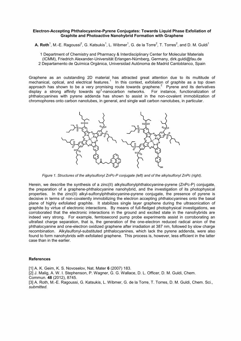
Electron-Accepting Phthalocyanine-Pyrene Conjugates: Towards Liquid Phase Exfoliation of Graphite and Photoactive Nanohybrid Formation with Graphene
A. Roth
1, M.-E. Ragoussi
2, G. Katsukis
1, L. Wibmer
1, G. de la Torre
2, T. Torres
2, and D. M. Guldi
1
1 Department of Chemistry and Pharmacy & Interdisciplinary Center for Molecular Materials (ICMM), Friedrich Alexander-Universität Erlangen-Nürnberg, Germany, [email protected]
2 Departamento de Quìmica Orgànica, Universidad Autònoma de Madrid Cantoblanco, Spain Graphene as an outstanding 2D material has attracted great attention due to its multitude of mechanical, optical, and electrical features.
1 In this context, exfoliation of graphite as a top down
approach has shown to be a very promising route towards graphene.2 Pyrene and its derivatives
display a strong affinity towards sp2-nanocarbon networks. For instance, functionalization of
phthalocyanines with pyrene addenda has shown to assist in the non-covalent immobilization of chromophores onto carbon nanotubes, in general, and single wall carbon nanotubes, in particular.
Figure 1. Structures of the alkylsulfonyl ZnPc-P conjugate (left) and of the alkylsulfonyl ZnPc (right).
Herein, we describe the synthesis of a zinc(II) alkylsulfonylphthalocyanine-pyrene (ZnPc-P) conjugate, the preparation of a graphene-phthalocyanine nanohybrid, and the investigation of its photophysical properties. In the zinc(II) alkyl-sulfonylphthalocyanine-pyrene conjugate, the presence of pyrene is decisive in terms of non-covalently immobilizing the electron accepting phthalocyanines onto the basal plane of highly exfoliated graphite. It stabilizes single layer graphene during the ultrasonication of graphite by virtue of electronic interactions. By means of full-fledged photophysical investigations, we corroborated that the electronic interactions in the ground and excited state in the nanohybrids are indeed very strong. For example, femtosecond pump probe experiments assist in corroborating an ultrafast charge separation, that is, the generation of the one-electron reduced radical anion of the phthalocyanine and one-electron oxidized graphene after irradiation at 387 nm, followed by slow charge recombination. Alkylsulfonyl-substituted phthalocyanines, which lack the pyrene addenda, were also found to form nanohybrids with exfoliated graphene. This process is, however, less efficient in the latter case than in the earlier. References [1] A. K. Geim, K. S. Novoselov, Nat. Mater 6 (2007) 183. [2] J. Malig, A. W. I. Stephenson, P. Wagner, G. G. Wallace, D. L. Officer, D. M. Guldi, Chem. Commun. 48 (2012), 8745. [3] A. Roth, M.-E. Ragoussi, G. Katsukis, L. Wibmer, G. de la Torre, T. Torres, D. M. Guldi, Chem. Sci., submitted.

Growth of embedded and protrusive graphene rings on 6H-SiC (0001) by thermal decomposition in argon gas atmosphere
Akkawat Ruammaitree, Hitoshi Nakahara, Yahachi Saito
Department of Quantum Engineering, Graduate School of Engineering,
Nagoya University, Nagoya 464-8601, Japan
Optical antennas are devices that efficiently convert the energy of free propagating radiation into localized energy and vice versa. The development of optical antennas can improve the efficiency of sensing, photodetection, light emission, spectroscopy and so on. Graphene rings are promising material for developing optical antennas because its plasmons have more electromagnetic confinement than metallic plasmons.
We grew epitaxial graphene by employing N-type Si-terminated 6H-SiC (0001) substrates. The sample was first cleaned by ultrasonic precleaning with acetone then mounted on the sample holder and put in a main chamber with the base pressure of ~10
-10 mbar. In order to remove oxide on the
, we deposited silicon around 2 monolayers on it. These silicon atoms are expected to react with oxide molecules and leave the surface in the form of SiOx when the sample was annealed at high temperature. Then the procedure for annealing SiC started by resistive heating in this UHV chamber. In case of annealing SiC substrate under Ar gas the sample had been transferred, without exposure to air, to another annealing chamber before annealed them by resistive heating under an Ar
gas pressure of 0.01-0.5 atm. The annealing temperature was in range of ~900 C to graphitization
temperature (1350 C - 1700 C) with steps of ~100 C (10~15 min per each step). The annealing temperature was measured by an optical pyrometer. After graphene was grown on the SiC substrates, the graphene morphology and shape on all samples are measured by AFM. We find that graphene rings can be grown under some conditions. Figure 1 shows a final annealing temperature and ambient Ar pressure graph displaying the condition which graphene rings can be grown on the SiC substrates. We found that graphene ring can be grown under the condition of Ar pressure of 0.05-0.1 atm (as indicated by triangle symbols). At this Ar pressure
and the final annealing temperature of 1550 C, embedded graphene rings can be grown on the samples (Figure 2 (a)-(c)). Under the condition of Ar pressure of 0.05 atm, we also try to anneal the
substrate with higher temperature (1650 C). Surprisingly, the protrusive graphene rings are found on the sample as shown in Figure 2 (d)-(f).
Figure 2 shows AFM topography and phase images of the samples which annealed under Ar
pressure of 0.05 atm with final annealing temperature of 1550 C (Figure 2 (a)-(c)) and 1650 C (0.05
atm 1650 C sample) (Figure 2 (d)-(f)) and Ar pressure of 0.3 atm with the final temperature of 1675 C
(Figure 2 (g)-(i)). In the case of 0.05 atm 1550 C sample (Figure 2 (a)-(c)), AFM phase image (Figure 2 (b)) shows there are many graphene rings on this sample (the bright regions indicate graphene regions). The AFM topographic image (Figure 2 (a)) shows the position of graphene rings is lower than that of SiC on the same terrace. Figure 2 (c) displays the magnification of the morphology of graphene ring in the rectangle in Figure 2 (a) reveals the graphene ring is embedded in SiC surface with the depth of
0.82 nm. For annealing with higher temperature (0.05 atm 1650 C sample), there are also many graphene rings are observed on the sample surface as shown in Figure 2 (e). The C diffusion length
and terrace width of this sample in average are about 1.2 m and 2-2.5 m, respectively. The AFM topographic image (Figure 2 (d)) reveals surprised results that the growth of graphene rings under this
condition gives us protrusive graphene rings. It is opposite to the case of 0.05 atm 1550 C sample (Figure 2 (a)-(c)) which showing the embedded graphene rings. Figure 2 (f) shows the magnification of a protrusive graphene ring image where the bright hollow hexagon is graphene region. This graphene ring is about 5.8 nm and 8.3 nm higher than the SiC terrace and pit inside, respectively. In the case of 0.3
atm 1675 C sample, the average of terrace width on this sample is about 1.25 m. There are only graphene stripes (no graphene island) on the terraces suggests that the C diffusion length is larger than
the terrace width (~1.25 m). Figure 2 (g) and (h) are AFM topographic and phase image, respectively
measured at position which contains wide terrace of about 3-6 m. Protrusive graphene islands are found on the wide terrace. Figure 2 (i) shows the magnification of morphology of protrusive graphene island in the rectangle in Figure 2 (g) reveals that protrusive graphene islands with the height of 2.2 nm
have no pit inside. It is different from graphene rings on the 0.05 atm 1650 C sample (Figure 2 (d)-(f)) which has a deep pit inside.
We found the growth of embedded and protrusive graphene rings on Si-terminated 6H-SiC (0001) by annealing SiC substrates under Ar gas pressure of 0.05-0.1 atm. The type of graphene rings
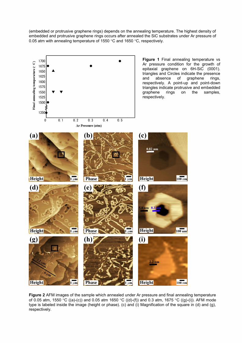
(embedded or protrusive graphene rings) depends on the annealing temperature. The highest density of embedded and protrusive graphene rings occurs after annealed the SiC substrates under Ar pressure of
0.05 atm with annealing temperature of 1550 C and 1650 C, respectively.
Figure 2 AFM images of the sample which annealed under Ar pressure and final annealing temperature
of 0.05 atm, 1550 C ((a)-(c)) and 0.05 atm 1650 C ((d)-(f)) and 0.3 atm, 1675 C ((g)-(i)). AFM mode type is labeled inside the image (height or phase). (c) and (i) Magnification of the square in (d) and (g), respectively.
Figure 1 Final annealing temperature vs Ar pressure condition for the growth of epitaxial graphene on 6H-SiC (0001). triangles and Circles indicate the presence and absence of graphene rings, respectively. A point-up and point-down triangles indicate protrusive and embedded graphene rings on the samples, respectively.

Vertical charge transport on the nano scale across a graphene–Si interface
R. Ruiter, K.S. Das, S. Parui, P. J. Zomer, B. J. van Wees, and T. Banerjee
Physics of Nanodevices, Zernike Institute for Advanced Materials, University of Groningen Nijenborgh 4
9747 AG Groningen the Netherlands [email protected]
Abstract The in-plane charge and spin transport characteristics of graphene have been extensively studied and high carrier mobility [1] and long spin relaxation length [2], at room temperature, demonstrated. Recently vertical device geometries that use a graphene/Si interface were fabricated, to explore charge transport in the out-of-plane direction in graphene [3]. Further, in different device geometries, graphene was used as a tunnel barrier [4] between two ferromagnetic electrodes in a magnetic tunnel junction as well as used as a spin-polarized tunnel barrier contact for electrical spin injection into silicon [5].
In order to fabricate functional devices from graphene, the current perpendicular to plane (CPP) transport needs to be understood. By using the Ballistic Electron Emission Microscope (BEEM) we can investigate CPP transport at the nanoscale. Figure 1a shows a schematic view of this technique. It is based on a Scanning Tunneling Microscope, but has an additional electrode at the back which records the BEEM current, IB. This current consists of electrons having the necessary energy and proper momentum at the metal-semiconductor (M-S) interface to surpass the Schottky barrier (SB), (see figure 1 b and c). The two orange cones visualize the momentum spread of the injected and collected electrons and leads to a high spatial resolution in BEEM. Furthermore, this technique allows us to simultaneously map the surface topography and the transmitted current in the buried layers of the device. Additionally, one can do spectroscopy by varying the voltage and keeping the tip at one location, in order to extract local SB heights.
Our device scheme is depicted in figure 2, where (multi layer) graphene flakes are scattered over the Si surface and is capped by Au. In this study we found that (multi layer) graphene forms a SB with the underlying n-type Si of 1.19 eV and shows very low leakage and good rectification (~10
6). Furthermore
on p-type Si it was found that the SB was similar. Normally one would expect the difference in barrier heights, on p- and n-type Si, to reflect the band gap of the semiconductor. However in this case extrinsic doping (e.g. water vapor) of the (multi layer) graphene, which causes a Fermi level shift, might be responsible for the deviation in SB. The nature and passivation of the underlying Silicon surface was found to influence the local BEEM transmission and the band alignments at the Gr/Si interface. References [1] Bolotin, K.I., Sikes, K.J., Jiang, Z., Klima, M., Fudenberg, G., Hone, J., Kim, P., and Stormer,
H.L., Solid State Communications, 146 (2008) 351–355. [2] Tombros, N., Jozsa, C., Popinciuc, M., Jonkman, H.T., and van Wees, B.J., Nature, 448 (2007)
571–574. [3] Yang, H., Heo, J., Park, S., Song, H.J., Seo, D.H., Byun, K.-E., Kim, P., Yoo, I., Chung, H.-J.,
and Kim, K., Science, 336 (2012) 1140-1143. [4] Cobas, E., Friedman, A.L., van’t Erve, O.M.J., Robinson, J.T., and Jonker, B.T., Nano Letters,
12 (2012) 3000–3004.
[5] Erve, O.M.J. van ’t, Friedman, A.L., Cobas, E., Li, C.H., Robinson, J.T., and Jonker, B.T.,
Nature Nanotechnology, 7 (2012) 737–742.

Figures
n-type Semiconductor
Metal
e-
IT
VT
IB
a)
STM tip
EF e-
b)
EF
MetalTip n-type SC
VT φ
B
V0
VT
IB
c)
Figure 1: a) Schematic representation of BEEM with the electrical connects. b) Energy schematics of the metal-semiconductor device along with the STM tip. The tip is biased negatively and a distribution of hot electrons is injected into the metal. c) The measured BEEM current IB, consists of electrons with proper energy and momentum to surpass the Schottky barrier (φB), as a function of the tunneling voltage VT.
Figure 2: Schematic side view of our device scheme. Hot electrons tunnel from the STM tip into the Au from which they travel to the graphene. The transmissted hot electron current at the graphene/Si interface is collected as the BEEM current IB.
Synthesis of Nitrogen-doped graphene with enhanced oxygen reduction activity by pyrolysis of graphene functionalized with imidazole derivatives
Virginia Ruiz1, Itxaso Azcune
1, Pedro Mª Carrasco
1, Hans J. Grande
1, Jani Sainio
2, Esko Kauppinen
2,
Maryam Borghei2
1CIDETEC-IK4, Centre for Electrochemical Technologies, Paseo Miramon 196, E-20009 Donostia-San
Sebastian, Spain 2Department of Applied Physics, Aalto University, Finland, Puumiehenkuja 2, FI-02150 Espoo, Finland
Abstract Replacing noble metal catalysts with cheaper and durable catalytic materials for the oxygen reduction reaction (ORR) is a key issue in the development of fuel cell technology. In this regard, nitrogen-doped carbon nanomaterials and in particular nitrogen-doped graphene have received increasing attention as effective metal-free electrocatalysts [1-5]. Nitrogen doping suppresses the density of states near the Fermi level of graphene thus opening a band gap between the conduction and valence bands. Nitrogen
graphene that participate in catalytic reactions such as the ORR. Nitrogen doping of graphene can be -synthesis. Post-synthesis doping methods
typically consist of plasma treatment or thermal annealing of graphene or graphene oxide with different nitrogen precursors such as NH3, melamine, urea or dicyandiamide or some ionic liquids (IL). Here, we have used an imidazolium-based poly(ionic liquid) (PIL), poly(3-butyl-1-vinylimidazolium bromide) (PBVIBr) as precursor (Figure 1) for nitrogen doping of graphene nanoplatelets (GNP) by thermal annealing of the corresponding PIL-functionalized GNP. To the best of our knowledge, pyrolysis of PIL-functionalized graphene to produce N-doped graphene has not been reported so far. In addition, two other imidazole derivatives of different nature and charge, the ionic liquid 1-butyl-3-methylimidazolium tetrafluoroborate (BMIBF4) and the neutral polymer poly(vinylimidazole) (PVI), Figure 1, have been investigated as precursors for nitrogen doping of GNP using the same strategy. Total nitrogen content and the chemical bonding configuration of nitrogen atoms in the N-GNP samples produced with the different precursors were examined by XPS, which confirms the incorporation of nitrogen atoms in the surface of N-GNP (Figure 2). All N-GNP showed enhanced electrocatalytic activity for oxygen reduction reaction in alkaline media compared to pristine GNP. The ORR electrocatalytic activity of N-doped GNP obtained from the three precursors (BMIBF4, PVI and PBVIBr) was examined and rationalized in terms of total nitrogen content, relative distribution of nitrogen bonding configurations, surface area and porosity of the resulting N-doped GNP. We will show how these parameters are influenced by the nature of the precursor. Interestingly, ORR catalytic activity in N-GNP did not correlate with total nitrogen content but was more affected by the BET surface area. Thus, the most active N-GNP materials were produced by pyrolysis of GNP functionalized with the ionic imidazolium-based nitrogen precursors, the IL and the PIL, which led to more porous and high surface area N-GNP. We believe that these results can be inspiring in the choice of suitable nitrogen precursors for doping carbon materials and hence achieve metal-free ORR electrocatalysts with enhanced activity. References [1] Wang H, Maiyalagan T, Wang X., ACS Catal., 2 (2012) 781. [2] Wei D, Liu Y, Wang Y, Zhang H, Huang L, Yu G., Nano Lett., 9 (2009) 1752. [3] Qu L, Liu Y, Baek JB, Dai L. ACS Nano, 4 (2010) 1321. [4] Geng D, Chen Y, Chen Y, Li Y, Li R, Sun X, et al., Energy Environ Sci., 4 (2011) 760. [5] Sheng ZH, Shao L, Chen JJ, Bao WJ, Wang FB, Xia XH. ACS Nano, 5 (2011) 4350.

Figures
Figure 1. Nitrogen precursors used for GNP functionalization and subsequent N-doping.
Figure 2. Core level high resolution N1s XPS spectra of N-GNP obtained from pyrolysis of GNP functionalized with the different nitrogen precursors: (A) BMIBF4, (B) PVI and (C) PBVIBr.
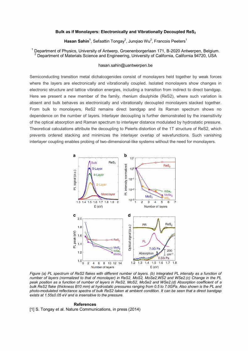
Bulk as if Monolayers: Electronically and Vibrationally Decoupled ReS2
Hasan Sahin
1, Sefaattin Tongay
2, Junqiao Wu
2, Francois Peeters
1
1 Department of Physics, University of Antwerp, Groenenborgerlaan 171, B-2020 Antwerpen, Belgium. 2 Department of Materials Science and Engineering, University of California, California 94720, USA
Semiconducting transition metal dichalcogenides consist of monolayers held together by weak forces
where the layers are electronically and vibrationally coupled. Isolated monolayers show changes in
electronic structure and lattice vibration energies, including a transition from indirect to direct bandgap.
Here we present a new member of the family, rhenium disulphide (ReS2), where such variation is
absent and bulk behaves as electronically and vibrationally decoupled monolayers stacked together.
From bulk to monolayers, ReS2 remains direct bandgap and its Raman spectrum shows no
dependence on the number of layers. Interlayer decoupling is further demonstrated by the insensitivity
of the optical absorption and Raman spectrum to interlayer distance modulated by hydrostatic pressure.
Theoretical calculations attribute the decoupling to Peierls distortion of the 1T structure of ReS2, which
prevents ordered stacking and minimizes the interlayer overlap of wavefunctions. Such vanishing
interlayer coupling enables probing of two-dimensional-like systems without the need for monolayers.
Figure (a) PL spectrum of ReS2 flakes with different number of layers. (b) Integrated PL intensity as a function of number of layers (normalized to that of monolayer) in ReS2, MoS2, MoSe2,WS2 and WSe2.(c) Change in the PL peak position as a function of number of layers in ReS2, MoS2, MoSe2 and WSe2.(d) Absorption coefficient of a bulk ReS2 flake (thickness B10 mm) at hydrostatic pressures ranging from 0.5 to 7.0GPa. Also shown is the PL and photo-modulated reflectance spectra of bulk ReS2 taken at ambient condition. It can be seen that a direct bandgap exists at 1.55±0.05 eV and is insensitive to the pressure.
References
[1] S. Tongay et al. Nature Communications, in press (2014)
Enhanced electrochromic properties of novel N-doped few layer graphene(N-FLG)@poly[Ni(salen)] nanocomposite
Cristina Freire
1, Mariana Araújo
1, Marta Nunes
1, Revathi Bacsa
2, Roberta Viana Ferreira
3, Eva
Castillejos4, Philippe Serp
2
1 REQUIMTE, Department of Chemistry and Biochemistry, Faculty of Sciences,
University of Porto, 4169-007, Porto, Portugal. 2Laboratoire de Chimie de Coordination UPR CNRS 8241, composante ENSIACET,
Toulouse University, 118 route de Narbonne, 31077 Toulouse, France 3Departamento de Química, Universidade Federal de Minas Gerais, Campus Pampulha,
31270-901 Belo Horizonte, Minas Gerais, Brazil 4Grupo de Diseño Molecular de Catalizadores Heterogéneos , C/ Marie Curie,
2, Cantoblanco, Madrid, E-28049 Spain
Abstract Graphene has attracted growing attention as a potential candidate for application in electrochemical and photo-electronics systems [1,2]. More recently, chemical doping of graphene as an approach to tailor its properties has attracted much attention, since it can overcome some limitations of pristine graphene (particularly, the absence of a semiconducting gap that may be a barrier to most electronic applications). Substitutional doping, which introduces heteroatoms in the carbon lattice of graphene, promotes the modulation of the electronic properties of graphene[3]; if pristine graphene is doped with nitrogen atoms, this material is converted into a n-type semiconductor and the band gap is opened. Electrochromic materials, which are functional materials whose optical properties can be controlled by electrical stimulus, have attracted a lot of interest from academia as well as from industry [4]. Currently, one of the main technological challenges is the development of low cost, flexible, portable and low energy consumption electronic devices for optical information. In this context, electroactive polymers - namely poly[M(salen)] polymers, which are electroactive polymers based on salen-type complexes have been highlighted as a promising class of electrochromic materials, since they combine mechanical flexibility along with the capability of color tuning [5,6]. However, some of their major drawbacks for successful commercialization are short term durability and adequate switching times. Recently, graphene and its derivatives have been reported to be very good candidates for conductive polymers-based composites since such materials combine the individual properties of conductive polymers e.g. superior electrical and optoelectronic properties [7] with those of graphene. Recent works show that the incorporation of graphene in conductive polymer matrixes promotes the improvement of the electronic transport behavior of the polymer, as well as the response times and the color efficiency[8,9]. For such bulk applications, few layer graphene (FLG) that consist of up to ten layers of graphene are interesting alternatives in view of their ease of handling and low cost. In this work, nanocomposites based in poly[Ni(salen)]-type electrochromic films and N-doped few layer graphene (N-FLG) were prepared, and the influence of the presence of N-FLG on the electrochemical and spectroscopic profiles and on the electrochromic properties of the nanocomposite formed was evaluated. Nitrogen doped FLG were prepared by fluidized bed chemical vapor deposition process by the decomposition of a mixture of ethylene and ammonia in the presence of a ternary oxide powder catalyst at 650°C [10]. The FLG powder was recovered after washing the powder in 35%HCl at 25°C. The structure was confirmed by TEM and Raman spectroscopy. The nitrogen content as determined both by XPS and chemical analysis was found to be around 3 at.%. The poly[Ni(salen)]-type films were obtained by the oxidative electropolymerisation of the respective Ni(II) salen complexes [10]. The polymeric nanocomposites were prepared by co-deposition of the electroactive film and N-FLG, by cyclic voltammetry, using flexible polyethylene terephthalate coated with indium-tin oxide (ITO/PET) as working electrode. The as-prepared nanocomposites were characterized by cyclic voltammetry, UV-Vis spectroscopy in situ, chronoabsorptometry and chronoamperometry. The as-prepared polymeric films showed a polyelectrochromic behaviour, changing their colours between yellow, green and russet (figure 1). The electrochemical characterisation revealed higher electroactive surface coverage for the film co-deposited with N-FLG, and the spectroscopic data
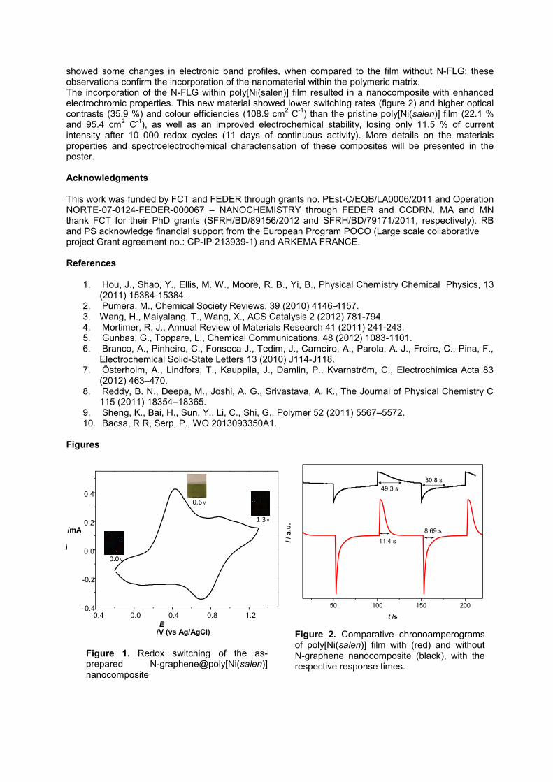
50 100 150 200
30.8 s
49.3 s
8.69 s
11.4 s
i /
a.u
.
t /s
showed some changes in electronic band profiles, when compared to the film without N-FLG; these observations confirm the incorporation of the nanomaterial within the polymeric matrix. The incorporation of the N-FLG within poly[Ni(salen)] film resulted in a nanocomposite with enhanced electrochromic properties. This new material showed lower switching rates (figure 2) and higher optical contrasts (35.9 %) and colour efficiencies (108.9 cm
2 C
-1) than the pristine poly[Ni(salen)] film (22.1 %
and 95.4 cm2 C
-1), as well as an improved electrochemical stability, losing only 11.5 % of current
intensity after 10 000 redox cycles (11 days of continuous activity). More details on the materials properties and spectroelectrochemical characterisation of these composites will be presented in the poster. Acknowledgments This work was funded by FCT and FEDER through grants no. PEst-C/EQB/LA0006/2011 and Operation NORTE-07-0124-FEDER-000067 NANOCHEMISTRY through FEDER and CCDRN. MA and MN thank FCT for their PhD grants (SFRH/BD/89156/2012 and SFRH/BD/79171/2011, respectively). RB and PS acknowledge financial support from the European Program POCO (Large scale collaborative project Grant agreement no.: CP-IP 213939-1) and ARKEMA FRANCE. References
1. Hou, J., Shao, Y., Ellis, M. W., Moore, R. B., Yi, B., Physical Chemistry Chemical Physics, 13 (2011) 15384-15384.
2. Pumera, M., Chemical Society Reviews, 39 (2010) 4146-4157. 3. Wang, H., Maiyalang, T., Wang, X., ACS Catalysis 2 (2012) 781-794. 4. Mortimer, R. J., Annual Review of Materials Research 41 (2011) 241-243. 5. Gunbas, G., Toppare, L., Chemical Communications. 48 (2012) 1083-1101. 6. Branco, A., Pinheiro, C., Fonseca J., Tedim, J., Carneiro, A., Parola, A. J., Freire, C., Pina, F.,
Electrochemical Solid-State Letters 13 (2010) J114-J118. 7. Österholm, A., Lindfors, T., Kauppila, J., Damlin, P., Kvarnström, C., Electrochimica Acta 83
(2012) 463 470. 8. Reddy, B. N., Deepa, M., Joshi, A. G., Srivastava, A. K., The Journal of Physical Chemistry C
115 (2011) 18354 18365. 9. Sheng, K., Bai, H., Sun, Y., Li, C., Shi, G., Polymer 52 (2011) 5567 5572. 10. Bacsa, R.R, Serp, P., WO 2013093350A1.
Figures
Figure 1. Redox switching of the as-prepared N-graphene@poly[Ni(salen)] nanocomposite
Figure 2. Comparative chronoamperograms of poly[Ni(salen)] film with (red) and without N-graphene nanocomposite (black), with the respective response times.
-0.4 0.0 0.4 0.8 1.2 -0.4
-0.2
0.0
0.2
0.4
i
/mA
E
0.0 V
0.6 V
1.3 V
/V (vs Ag/AgCl)

Functional Graphene-Polyelectrolyte Thin Films Formed By Hydrogen Bonding
A.Y.W. Sham1, S. M. Notley
2
1Department of Applied Mathematics, Research School of Physics and Engineering, The Australian
National University, Canberra, ACT 0200, Australia 2Department of Chemistry and Biotechnology, Swinburne University Technology, Hawthorn, VIC 3122,
Australia [email protected]
Abstract This study focuses on incorporating surfactant assisted exfoliated pristine graphene nanoparticles into polyelectrolyte multilayers using hydrogen bonding to create functional thin films. Electrically conducting thin films are essential for a variety of applications including solar cells, photonics and flexible electronics. Traditional inorganic thin film materials are reaching their technological limit. Organic based thin film systems that incorporate innovative materials are increasingly being studied in an effort to enhance electrical, thermal, optical and mechanical properties and provide added functionality. Recently, graphene, a carbon allotrope consisting of single layer macroscopic carbon sheets, has attracted considerable interest in a range of research fields due to its unique 2D structure [1]. As a consequence of this unique structure, graphene possesses remarkable electrical conductivity, tensile strength, flexibility and optical transmittance, making it ideal for integration into thin films. Previous studies have formed thin films from the layer by layer addition of oppositely charged polymers and graphene sheets through strong electrostatic interactions [2]. This study focuses on incorporating graphene nanoparticles into polyelectrolyte multilayers using hydrogen bonding. First, dispersions of pristine graphene nanoparticles were created from synthetic graphite using a method of surfactant-assisted exfoliation [3]. Thin films containing the anionic polyelectrolyte, polyacrylic acid and graphene nanoparticles were then constructed using the layer by layer approach [4]. Films were prepared using dip coating at low pH and the Quartz Crystal Microbalance (QCM) apparatus was used to monitor the deposition kinetics and adsorbed amount. A flow diagram of the process used to create and characterize graphene-polyelectrolyte thin films through hydrogen bonding is shown in Figure 1. A range of analytical techniques were used to characterize the resultant film composition, surface features and mechanism of formation for the thin films. QCM measurements, Raman spectra and UV visible spectra indicate the successful formation of thin film multilayers incorporating polyacrylic acid and surfactant exfoliated graphene nanoparticles, suggesting hydrogen bonding facilitates film formation in such systems. However, atomic force microscopy imaging, in addition to optical microscopy indicated partial dewetting of the films from the silica substrates. It was also demonstrated that film growth proceeded exponentially during deposition of the first few bilayers, but became linear as significant numbers of bilayers were adsorbed. These results give an indication as to the quality and characteristics of thin films containing graphene nanoparticles, and formed through layer by layer deposition in addition to the mechanism of graphene multilayer thin film formation. These insights may guide further studies regarding graphene-based thin films. References [1]. K. S. Novoselov, A. K. Geim; S. V. Morozov, D. Jiang, Y. Zhang, S. V. Dubonos, I. V. Grigorieva, A.
A. Firsov, Science, 5696 (2004) pp. 666-669.
[2]. S. M. Notley, J. Colloid Interface Sci, 1 (2012), pp. 35-40.
[3]. S. M. Notley, Langmuir, 40 (2012) pp. 14110-14113.
[4]. G. Decher, J. D. Hong, Makromol. Chem-M. Symp., 46 (1991) pp. 321-327.
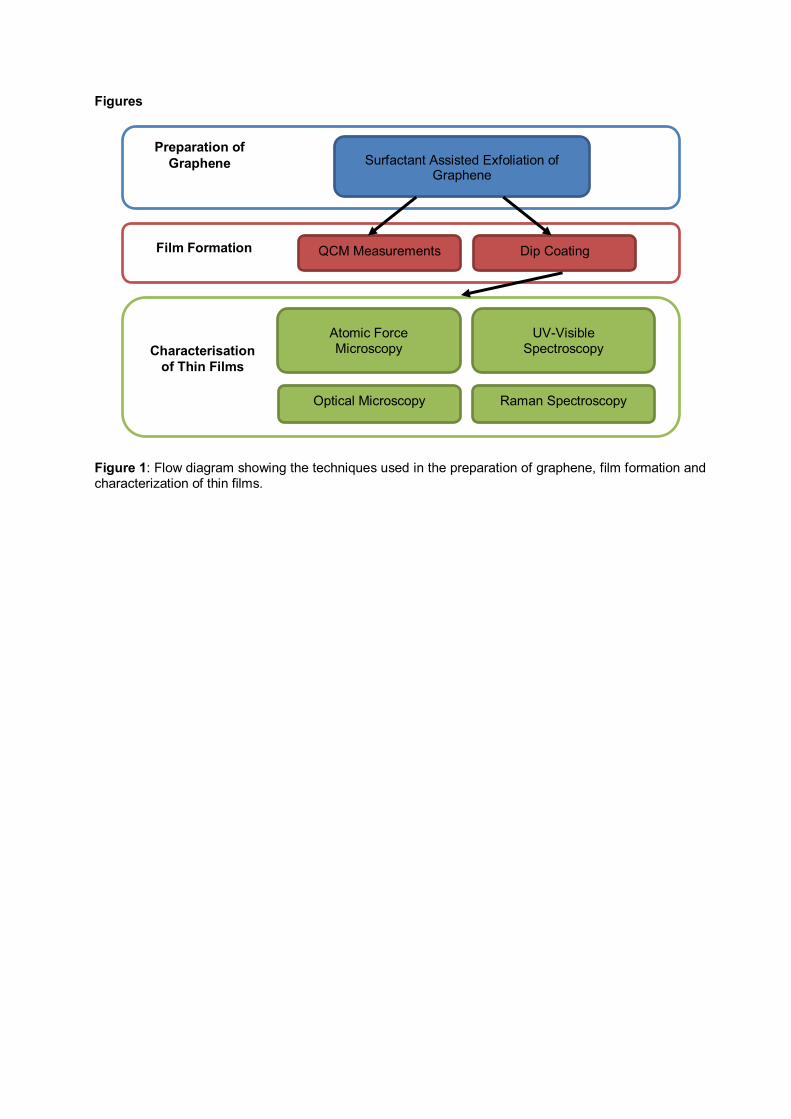
Figures Figure 1: Flow diagram showing the techniques used in the preparation of graphene, film formation and characterization of thin films.
Surfactant Assisted Exfoliation of Graphene
QCM Measurements Dip Coating
Raman Spectroscopy
UV-Visible Spectroscopy
Optical Microscopy
Atomic Force Microscopy
Preparation of
Graphene
Film Formation
Characterisation
of Thin Films

Photoinduced open circuit voltage in graphene-based polythiophene:fullerene solar cells
Faranak Sharifi, Giovanni Fanchini
Department of Physics & Astronomy, University of Western Ontario, London, Ontario, N6A 3K7, Canada
We observed significant photoinduced increase in the open circuit voltage of thin
polythiophene:fullerene bulk heterojunction solar cells assembled on transparent layers of graphene,
which correspond to similar changes in the electronic work function of the graphene electrodes.
Graphene thin films were prepared using RNA as a surfactant with a method developed by us [1]. We
used Kelvin Probe Force Microscopy, in the dark and under illumination [2], to demonstrate that the
observed photoinduced changes (see Figure 1) are in good agreement with a dynamic graphene-
insulator-metal model that, in addition to the customary assumptions of metal-insulator-metal models for
thin film solar cells, takes into account the specific photophysical properties of graphene as a zero-band
gap semiconductor. Band energy offset models that were previously used to model the open circuit
voltage in graphene-based solar cells can be dismissed.
References [1] F. Sharifi, R. Bauld, M.S. Ahmed, and G. Fanchini, Small 8, 699 706 (2012) [2] F. Sharifi, R. Bauld, and G. Fanchini, J. Appl. Phys. 114 , 144504 (2013) Figure 1
Band energy level diagram of graphene-based solar cells showing the increase of Work Function and, consequently, open circuit voltage measured by KPFM under illumination.

Electronic Transport Behavior in High-Quality Twisted Bilayer Graphene Nanoribbons
Haoliang Shen,1,2
Alessandro Cresti,3
Fabrice Iacovella,2
Walter Escoffier,2
Yi Shi,1
Xinran Wang,1
Bertrand Raquet2
1National Laboratory of Solid State Microstructures and School of Electronic Science and
Engineering, Nanjing University, 22 Hankou Road, Nanjing 210093, P. R. China2
Laboratoire National des Champs Magnétiques Intenses, INSA UPS UJF CNRS, UPR 3228, Université de Toulouse,143 av. de Rangueil, 31400 Toulouse, France
3IMEP-LAHC (UMR CNRS/INPG/UJF 5130), Grenoble INP Minatec, 3 Parvis Louis Néel,
BP 257, F-38016 Grenoble, France
[email protected], [email protected]
By scaling down the width of 2D material Graphene, a new 1D carbon system rises up,
well-known as Graphene Nanoribbon (GNR). Besides the many merits inherited from its
ancestor-Graphene, GNR has one exceptional advantage over the zero-gap material
graphene: a bandgap is arisen due to the transverse confinement, which makes GNR more
promising for logical devices and electrical application. Therefore, it is essential to understand
the electronic property of GNR.
Theoretical work have revealed that the band structure of GNR is highly dependent on its
width and edge geometry (chirality) [1,2]. Recently several experimental work have stressed
on this issue[3-5]: lithography made GNR is proved to have rough edges, thus introducing a
“transport gap” other than the intrinsic confinement gap [3]. The charge transport is more
dominated by the edge disorder, therefore making it less ideal to study the intrinsic effects of
confinement. R. Ribeiro et al. firstly made efforts to study the quantum transport in
lithographically patterned GNR with width around 70-100nm [4]. The results unveil the onset of
magnetoelectronic subbands, edge currents and quantized hall conductance, also bringing the
evidence of the valley degeneracy lifting due to the electronic confinement. However, the width
of the studied ribbons is so wide that the confinement effect is less significant and bulk effect
still exists. In this region, chirality plays feeble impact. Another work is done on chemically
derived GNRs [6] with width around 11nm [5]. However, for this study, the conductance is far
away from the supposed value in quasi-ballistic regime, probably due to the underlying
disorders inside this kind of GNR. And here the magnetoconductance is not able to reach the
quantum hall regime.
In this work, we start with sonochemical derived graphene nanoribbons, originally unzipped
from multi-wall carbon nanotubes, with width around 20nm exhibiting ultra-smooth edges
[7-10]. Noteworthily, it has been reported that 70% of the final products with this unzipping
method are twisted bilayer GNRs [8], and the twist angle is randomly distributed. By probing
the two-terminal magnetoresistance of the as-made GNRs under pulse magnetic field up to
55T, un unusual reproducible quantized conductance value shows up and we bring the
evidence that the carrier transport in twisted bilayer GNR is ruled by two parallel layers both
conducting with very close carrier densities. The two layers both enter into quantum hall
regime at almost the same magnetic field. And the total magnetoconductance is contributed by
the two “independent” layers, with each layer still behaving like one monolayer GNR’s
spectrum. We are now attempting to unveil the magnetic band structure on each layer.

References:
[1] K. Nalada et al., Phys. Rev. B 54, 17954 (1996)
[2] K. Wakabayashi et al., Phys. Rev. B 59, 8271 (1999)
[3] M.Y. Han et al., Phys. Rev. Lett. 104, 056801 (2010)
[4] R. Ribeiro et al., Phys. Rev. Lett. 107, 086601 (2011)
[5] J. Poumirol et al., Phys. Rev. B 82, 041413(R) (2010)
[6] X. Li et al., Science 319, 1229 (2008)
[7] L. Jiao et al., Nature Nanotech. 5, 321 (2010)
[8] L. Xie et al., J. Am. Chem. Soc. 133, 10394 (2011)
[9] C. Tao et al., Nature Phys. 7, 616 (2011)
[10] X. Wang et al., Nature Nanotech. 6, 563 (2011)
Figures:
Fig 1. Conductance versus back-gate
voltage of one typical sample device
during the cooling process. G0=2e2/h.
The sharp dip around the charge
neutrality point indicates the transport is
dominated by confinement, other than
edge disorder.
Fig 2. Magneto-Conductance of the same
device at 4.2K in p-doped region. At high
doping level, the magneto- conductance
shows a plateau around 3.5 e2/h (Contact
resistance still included).
Enabling the low temperature CVD growth of graphene using Alloy Catalyst and graphene
induced abnormal grain growth of Cu-Ag alloy
Hae-A-Seul Shin1, JaeChul Ryu
2,3, SeungMin Cho
3, Byung Hee Hong
2,* and Young-Chang Joo
1,*
1Department of Materials Science & Engineering, Seoul National University, Seoul 151-744, Korea
2Department of Chemistry, Seoul National University, Seoul 151-747, Korea
3SAMSUNG TECHWIN Co., Ltd., Seongnam 463-400, Korea
Abstract
Graphene, a two-dimensional crystalline structured material has been spotlighted from many
researchers because of its fascinating electrical, mechanical, optical, thermal properties.[1-6]
One of the
major challenges for the practical application of graphene has been the synthesis of large scale and
uniform films with higher quality at lower temperatures. New catalytic design for graphene synthesis is
essential to lower the synthesis temperature and improve the uniformity of graphene. Here, we
demonstrate that the use of Ag-plated Cu substrates is very useful to synthesize the high quality
graphene films via chemical vapor deposition (CVD) of methane gas at the temperature as low as 900
. In addition, we investigated that the abnormal grain growth of Cu with more than 1 mm2 of grain size
was induced by the graphene synthesis and this phenomena was occurred only for the Cu-Ag alloy foil
among various type of Cu foils.
Graphene was synthesized on the Cu foil and Ag plated Cu foil at 800 , 900 and 1000 using
thermal chemical vapor deposition system. The synthesized graphene was inspected by optical
microscope and Raman spectroscopy for the comparison of synthesis quality with the coverage of
graphene film and the optimization of growth condition. Transmission electron microscope (TEM) was
employed to determine crystal quality and uniformity of graphene and its domain size. For the analysis
of Cu foil after graphene synthesis, scanning electron microscope (SEM) with Energy dispersive x-ray
spectrometer, Dynamic-secondary ion mass spectrometry (D-SIMS) electron backscatter diffraction
(EBSD) were used.
The uniform graphene film with full coverage was synthesized on the Ag plated Cu foil at 900 and
this synthesis temperature was much lower as compared with the common synthesis temperature of
graphene on Cu.[7]
Synthesis state of highly uniform monolayer graphene was confirmed from the
mapping analysis by Raman spectroscopy and TEM analysis. Graphene synthesis was enhanced with
the increasing of Ag plating thickness for the thin Ag plating, while non-uniformity of graphene was
increased for the thick Ag plating. High quality graphene without defects or bilayer sites was achieved
with optimization of Ag plating thickness. The plated Ag diffuses into Cu and the formation of uniform
Cu-Ag alloy was demonstrated by various analyses and this optimized Cu-Ag alloy controlled the
formation of multilayer nucleation, leading to the lower synthesis temperature with enhanced monolayer
coverage. In addition, the abnormal grain growth of Cu into cube texture with mm2 scale of giant grain
size was observed only on Cu-Ag alloy with graphene synthesis. The ratio of (100) was exceeded more
than 90 % for Cu-Ag with graphene synthesis and this phenomena was not occurred if one of the
condition of Ag or graphene was insufficient. In this talk, we report this unusual phenomena in detail and
the role of Ag for low temperature CVD growth of high quality graphene.
References
[1] K. S. Novoselov, A. K. Geim, S. V. Morozov, D. Jiang, Y. Zhang, S. V. Dubonos, I. V. Grigorieva, A.
A. Firsov, Science, 306 (2004) 666-669.
[2] Y. Zhang, Y.-W. Tan, H. L. Stormer, P. Kim, Nature, 438 (2005) 201-204.
[3] A. K. Geim, K. S. Novoselov, The rise of graphene. Nat. Mater., 6 (2007) 183-191.
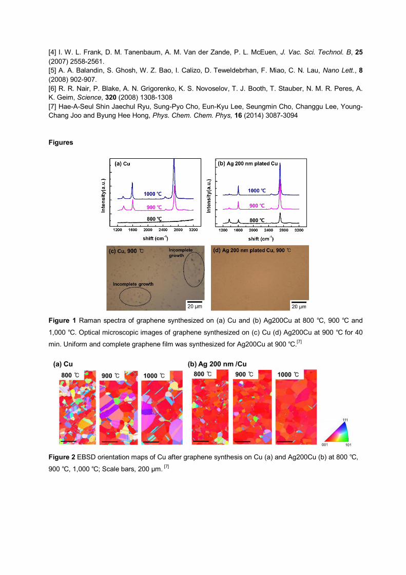
[4] I. W. L. Frank, D. M. Tanenbaum, A. M. Van der Zande, P. L. McEuen, J. Vac. Sci. Technol. B, 25
(2007) 2558-2561.
[5] A. A. Balandin, S. Ghosh, W. Z. Bao, I. Calizo, D. Teweldebrhan, F. Miao, C. N. Lau, Nano Lett., 8
(2008) 902-907.
[6] R. R. Nair, P. Blake, A. N. Grigorenko, K. S. Novoselov, T. J. Booth, T. Stauber, N. M. R. Peres, A.
K. Geim, Science, 320 (2008) 1308-1308
[7] Hae-A-Seul Shin Jaechul Ryu, Sung-Pyo Cho, Eun-Kyu Lee, Seungmin Cho, Changgu Lee, Young-
Chang Joo and Byung Hee Hong, Phys. Chem. Chem. Phys, 16 (2014) 3087-3094
Figures
Figure 1 Raman spectra of graphene synthesized on (a) Cu and (b) Ag200Cu at 800 , 900 and
1,000 . Optical microscopic images of graphene synthesized on (c) Cu (d) Ag200Cu at 900 for 40
min. Uniform and complete graphene film was synthesized for Ag200Cu at 900 .[7]
Figure 2 EBSD orientation maps of Cu after graphene synthesis on Cu (a) and Ag200Cu (b) at 800 ,
900 , 1,000 [7]

Integration of graphene sheets and carbon nanotubes as fillers in polymer matrices,
and their implementation.
Michael Shtein, Roey Nadiv, Matat Buzaglo, Keren Kahil and Oren Regev
Ilse Katz Institute for Nanoscale Science & Technology, Ben-Gurion University, Beer Sheva, Israel.
The unique properties and growing availability of nanoscale fillers (NF) such as graphene sheets (GS)
or carbon nanotubes (CNT) have driven research aimed at large-scale production and
commercialization of NF-based polymer composite materials (NPC) with enhanced thermal, mechanical
or electrical properties at low filler loading. The major hindrances in successful utilization of NPC are
shortage of effective methods for dispersion of individual NFs in polymeric matrices and NF
concentration determination in multicomponent solutions. To address these issues we developed a
thermogravimetric-spectroscopy approach to accurately determine the NF concentration in dispersion
[1]. Consequently, a conventional spectroscopy-based concentration calibration plot is constructed for
simple and swift use in further concentration measurements (Figure 1). Such true concentration analysis
is crucial for studying the concentration property relationship.
High GS (0.7 mg /mL) and CNT (5mg/mL) concentrations in water were prepared by optimizing the
nature of dispersant and the type of ultrasonic generator [2]. These NF were further employed to
fabricate NPC with enhanced properties:
Electrical conductivity: A hybrid of GS-CNT was employed to fabricate conductive transparent
electrodes for a molecularly-controlled solar-cell with an open-circuit voltage of 0.53V [2].
Mechanical properties: Upon loading of individual CNTs in the polymer matrix using a novel dispersion
method, we achieved a record fracture toughness enhancement (150%, Figure 2) at very low (0.1
vol.%) filler concentration. For the first time, we showed a coherent quantitative correlation between the
fracture toughness and the surface roughness. The failure mechanism (pullout or fracture) is predicted
by the slope of the surface roughness vs. fracture toughness curve [3].
Thermal properties: We demonstrated that beyond GS concentration, its size and surface treatment
affect the thermal properties of GS-epoxy NPC. An excellent NF distribution is achieved by non-covalent
modification of the NFs surface and a new dispersion approach. The structural parameters of the NF,
i.e., lateral size and thickness strongly affect the thermal conductivity of the composites. When
optimized, they result in a record thermal conductivity, (6.5W/mK, 3750% enhancement) of the NPC
(Figure 3). Finally, optimized GS/nano Boron-nitride/epoxy hybrid composites with synergistic effect and
tunable electrical properties, suitable for different thermal management applications, were
demonstrated.
References
[1] Michael Shtein, Ilan Pri-Bar and Oren Regev, Analyst, 138 (2013), 1490-1496. [2] Matat Buzaglo, Michael Shtein, Sivan Kober, Robert Lovrincic, Ayelet Vilan and Oren Regev, Phys. Chem. Chem. Phys.,15 (2013), 4428-4435. [3] Michael Shtein, Roey Nadiv, Noa Lachman, H. Daniel Wagner and Oren Regev, Composites Science and Technology, 87 (2013), Pages 157 163.

Figure 1: Calibration curve of GS concentration: a UV-vis absorption intensity vs TGA-determined GS concentration. The extracted extinction coefficient is the slope. Circles and triangles correspond to two different stock solutions
Figure 2: Fracture toughness as a function of nanotubes' volume percent.
Figure 3: Thermal conductivity (k) of the composites as a function of filler type and volume fraction*(same units as
fig 2 abscissa/ BN in red and larger symbols).
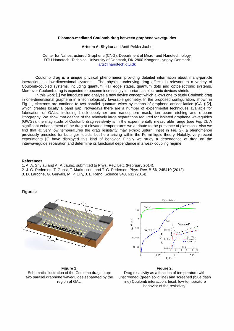
������������ ������� ��� ���� ������ �������
����� �� ����������������������� ��
���������������� �� ���������������������������������������������������� ��!"����������!��������"��#���� �������������$�%&''�$������( ��) ��������
����*�������+�� +��
�� ���)������ �� �� � ��, ��� ����� �������������#������������� ����������� ��)� � ���� ������������������� � �� � ��-����������� � � ����+ � � !� � �� ���� � ���� ��� � ���� � ����� � �� � ��#��� � �� � � � #���� � ���� ���)��� ��� �� ����� � ���� ���� �, ��� ��.��� ���������� �, ��� ������ ���� ������������� �� ����+����#���� ���)���������/��������)�������������� ������������������������#����������+�
0�������-����123�-������� ���������� 4����-��#����������-���������-���������� � ��� ���)����������������������������������������������� ���#���)������� +�0������������������� �����������-����5��+�2�������������������������-����������, ��� ��-����) ����������������������������������(��1%3�-����������� ������ �� �)�������+ ���-��� �� ��� ��� �� �� �)� ��� �/�������� � �����, ���#����)� � �����)�������� � �� � ��(�� � ���� ���� � )���������� �� � ��� � �������� � ����� � ��� � )�� � ������ � ��� � �)������������ +�6����-�����������������������#� ������������������, �����������������������-�#� �����6�������������� ������� ���)������������#�� ����������/��������� ���� ��)����������5��+�%�+��������������������������������������#���������� ���-������) �������������������������+������-���� � ���� ��� �#� � ��-� ������ �� � �� ����� � ������#�� ��� �/��)�� � �� �� � ����� � �� �5��+ �%�� � � �����������#�� �� �������������( ���������, �����) �������������-���������5������, ������� +�����)� ��#� �����/������� � 173 � ��# � ������ � � ���� � ���� � �� � )��#���+ � 5����� � - � �� � � � � ������ � �� � ���� � �� � ������-�#� ����������������������������� ���������������������-����� ����������+
������2+��+��+�8� �� ������+�+��� ����� )���������� �+�9#+�(��+��5)� �� �%'2:�+%+��+��+�������!+�� �����!+����� ���������!+��+�������� �+�9#+�;�����%:<:2'��%'2%�+7+��+�(��������+���#������+�+�(��� ���+�(+�9����8����� ! ��=72��%'2:�+
"�����#
"���� $#8����������� ����������������� ���)�������� �>
�-�����������������-�#� ������������) ��������������(+
"���� %#�����������#�� ������� ���������������� ��-���
����������������������������������)� ������������ ���)�����������+�0���>���-������� �
)��#����������������#�� +
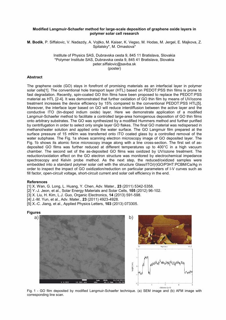
Modified Langmuir-Schaefer method for large-scale deposition of graphene oxide layers inpolymer solar cell research
M. Bodik, P. Siffalovic, V. Nadazdy, A. Vojtko, M. Kaiser, K. Vegso, M. Hodas, M. Jergel, E. Majkova, Z. Spitalsky*, M. Omastova*
Institute of Physics SAS, Dubravska cesta 9, 845 11 Bratislava, Slovakia*Polymer Institute SAS, Dubravska cesta 9, 845 41 Bratislava, Slovakia
[email protected](poster)
Abstract
The graphene oxide (GO) stays in forefront of promising materials as an interfacial layer in polymer solar cells[1]. The conventional hole transport layer (HTL) based on PEDOT:PSS thin films is prone to fast degradation. Recently, spin-coated GO thin films have been proposed to replace the PEDOT:PSS material as HTL [2-4]. It was demonstrated that further oxidation of GO thin film by means of UV/ozone treatment increases the device efficiency by 15% compared to the conventional PEDOT:PSS HTL[5].Moreover, the interface layer based on GO will reduce interdiffusion between the active layer and the conductive ITO (tin-doped indium oxide) layer. Here we demonstrate application of a modified Langmuir-Schaefer method to facilitate a controlled large-area homogenous deposition of GO thin films onto arbitrary substrates. The GO was synthesized by a modified Hummers method and further purified by centrifugation in order to select only single layer GO flakes. The final GO material was redispersed in methanol/water solution and applied onto the water surface. The GO Langmuir film prepared at the surface pressure of 15 mN/m was transferred onto ITO coated glass by a controlled removal of thewater subphase. The Fig. 1a shows scanning electron microscopy image of GO deposited layer. The Fig. 1b shows its atomic force microscopy image along with a line cross-section. The first set of as-
a high vacuum chamber. The second set of the as-deposited GO films was oxidized by UV/ozone treatment. The reduction/oxidation effect on the GO electron structure was monitored by electrochemical impedance spectroscopy and Kelvin probe method. As the next step, the reduced/oxidized samples were embedded into a standard polymer solar cell with the structure Glass/ITO/(r)GO/P3HT:PCBM/Ca/Ag in order to inspect the impact of GO oxidization/reduction on particular parameters of I-V curves such as fill factor, open-circuit voltage, short-circuit current and solar cell efficiency in the end.
References[1] X. Wan, G. Long, L. Huang, Y. Chen, Adv. Mater., 23 (2011) 5342-5358.[2] Y.-J. Jeon, et al., Solar Energy Materials and Solar Cells, 105 (2012) 96-102.[3] X. Liu, H. Kim, L.J. Guo, Organic Electronics, 14 (2013) 591-598.[4] J.-M. Yun, et al., Adv. Mater., 23 (2011) 4923-4928.[5] X.-C. Jiang, et al., Applied Physics Letters, 103 (2013) 073305.
Figures
Fig. 1 - GO film deposited by modified Langmuir-Schaefer technique. (a) SEM image and (b) AFM image with corresponding line scan.

Broadband deep-ultraviolet third-harmonic generation in multilayer graphene and its application to few-cycle pulse measurement by THG d-scan
Francisco Silva
1, Miguel Miranda
2 and Helder Crespo
1
1IFIMUP-IN and Dep. Física e Astronomia, Univ. do Porto, R. Campo Alegre, 4169-007 Porto, Portugal.
2Department of Physics, Lund University, P.O. Box 118, SE-221 00 Lund, Sweden.
[email protected], [email protected] Abstract: We report on broadband deep-ultraviolet (DUV) third-harmonic generation (THG) in multilayer CVD-grown graphene pumped by few-cycle pulses from a Titanium:Sapphire laser oscillator. An enhan-ced nonlinear optical response compared to near-surface THG in the bare (uncoated) substrate is clearly observed. We apply this process to the complete characterization (amplitude and phase) of the low-energy few-cycle (7.1 fs FWHM) pump pulses using the new technique of THG dispersion-scan. I. Introduction Graphene is an extremely promising material owing to its unusual properties. Amongst them, it possesses an exceptionally high nonlinear optical susceptibility [1], which has motivated further investigation of its performance in various nonlinear optical processes. Achieving ultra-broadband third-harmonic generation (THG) at low intensities is currently a demanding task and the strong, near-dispersionless nonlinear response of graphene should be very suitable for this purpose. The possibility of using a multilayer graphene film for enhanced THG [2] adds to its interest as a practical material. Furthermore, the promise of graphene retaining its extremely broadband nonlinearity due to lack of macroscopic phase-matching (each layer is sub-nm thick) makes it highly attractive for ultrafast applications. THG in few-layer graphene pumped by 320 fs pulses at 1720 nm resulted in visible pulses at 573 nm, where a quadratic dependence of the THG signal on the number of layers was observed [3]. THG in monolayer graphene pumped with 50 fs pulses at 789 nm enabled probing structural properties of graphene [4]. In a previous communication, we reported on broadband THG in graphene pumped by 7 fs few-cycle laser pulses [5]. In this work we demonstrate THG enhancement from multilayer graphene compared with near-surface THG under loose focusing conditions and over a large bandwidth in the deep-ultraviolet (DUV). Furthermore, we use this signal to make a pulse measurement of a femtosecond oscillator using a THG dispersion-scan (d-scan) setup and further compare these results to a standard SHG d-scan measurement [6]. Pulse characterization through d-scan is based on the fact that when a pulse undergoes a nonlinear conversion process (e.g. SHG), the resulting spectral intensity has a well-defined dependence on the input spectral phase. This way, one only needs to measure the resulting spectrum for different input spectral phases to be able to retrieve the initial spectral phase. THG d-scan is desirable as an alternative to SHG d-scan due to the possibility of gating spectra over an octave in bandwidth without overlapping the nonlinear signal and the fundamental, as well as for its potential for measuring longer wavelength few-cycle mid-IR lasers. II. Experimental setup and results For this study, an ultra-broadband Ti:Sapphire laser oscillator (Femtolasers Rainbow CEP) was used. As shown in Fig. 1, the beam was sent through a pair of BK7 glass wedges (8º angle) for variable dispersion adjustment and fine-tuning and then underwent 4 bounces off ultra-broadband double-chirped mirrors (IdestaQE) introducing negative dispersion. The beam was then focused on the sample
using a spherical silver mirror with 5 cm focal length. The focal spot was approx. 5 m (1/e2 width) with
a peak intensity of approximately 100 GW/cm2. The sample is a nickel-grown multilayer graphene
(MLG) film transferred to an optical quality fused silica substrate. The film is non-uniform and composed of multilayer domains of graphene having between 1 to 7 layers. To detect the generated third-harmonic we used a prism pair to spatially block the fundamental radiation prior to coupling the THG signal into a fiber-coupled spectrometer (Ocean Optics HR4000). Using this setup we first studied the efficiency of the THG signal. Due to the inhomogeneity of the sample, the signal from MLG varies greatly in intensity across its surface, depending on the number of layers in the location being irradiated. When optimizing for the strongest signal, it is possible to obtain approximately 20 times higher intensity than for locations in the substrate not covered with multilayer graphene, whereas no such enhancement has been observed for a copper grown single-layer graphene sample. This 20-fold enhancement in the THG signal is significant and eases the requirements for some applications that would otherwise need extremely tight focusing. The right plot in Fig. 1 shows the THG spectrum as a function of incident average power, revealing a cubic dependence on the input pulse intensity, as expected. One useful, widespread application of broadband THG generation is femtosecond pulse characterization. Owing to its simplicity, the required parts to make a dispersion-scan measurement were already in place, so we used this exact setup to measure the incident pulses by THG d-scan. Additionally, by simply replacing

the MLG sample with a SHG crystal (5- m-thick BBO) we were also able to measure the corresponding SHG d-scan traces [6] in order to compare the two methods (Fig. 2). By recording the THG spectrum for varying BK7 wedge insertions we obtained a 2D THG d-scan trace (Fig. 2a) that, like its SHG counterpart (Fig. 2c), contains enough information to fully retrieve the pulse phase using the algorithm described in detail in [6], modified for the THG nonlinearity. An excellent agreement between pulses retrieved using the two methods is observed, as shown in Figs. 2e and 2f. III. Conclusions We obtained efficient THG of few-cycle pulses over a broad bandwidth in the DUV (230-305 nm) from nickel-grown graphene multilayer samples transferred to an optical substrate. We found that this signal is readily observable for nJ-level pulses even in loose focusing conditions (i.e. not requiring short and unpractical focal lengths) and subsequently applied this process to few-cycle pulse characterization with zero changes introduced in the previous setup. We demonstrated pulse measurement and retrieval through THG d-scan and compared it to SHG d-scan, achieving excellent agreement. THG d-scan is a promising new technique for characterizing single-cycle pulses and few-cycle mid-IR laser sources. References [1] E. Hendry, P. J. Hale, J. Moger, A. K. Savchenko, S. Mikhailov, Phys. Rev. Lett. 105 (2009) 97401. [2] S.A. Mikhailov, Physica E: Low-dimensional Systems and Nanostructures 44 (2012) 924. [3] N. Kumar, J. Kumar, C. Gerstenkorn, R. Wang, H.-Y. Chiu, A.L. Smirl, and H. Zhao, Phys. Rev. B
87 (2013) 121406(R). [4] S. Hong, J. Dadap, N. Petrone, P. Yeh, J. Hone, and R. Osgood, Phys. Rev. X 3 (2013) 021014. [5] F. Silva, M. Miranda, and H. Crespo, Fr2.2, Ultrafast Optics, Davos, Switzerland, 8 March 2013. [6] M. Miranda, T. Fordell, C. Arn 20 (2012) 688. Figures
Fig. 1. (Left) THG d-scan setup used in this work, composed of 3 main blocks: a) variable dispersion compensation, b) nonlinear stage (THG/SHG), c) wavelength separation and spectral measurement. (Right) Measured THG spectrum in multilayer graphene as a function of incident average power.
Fig. 2. Experimental results: a) Measured THG d-scan in graphene. b) Retrieved THG d-scan. c) Measured SHG d-scan. d) Retrieved SHG d-scan. e) Black: spectral intensity. Red: Retrieved phase for shortest pulse, SHG-d-scan. Blue: Retrieved phase for shortest pulse, THG-d-scan. f) Temporal intensity corresponding to the spectrum and phases in Fig. 2e. Blue line: THG d-scan (7.1 fs FWHM). Red line: SHG d-scan (7.1 fs FWHM).

���������������� ����� ������������������������ ��������� ���
������������������������������������� �� �������������������������������
�������������������������� �����������������!���"������"�#$�%&�'���������(���������������(������������)����!��������������*�����"��(���"������'����!��#$�%&�'���������(����
&��������������������������+������������+������"���++�"�,�(��-���$#.%�+�������(����
���)�/�������
���������
0����������1�������2���!�������,0+3�-���2����+�(������4(������5���!��!�1�2�����������
�������2��*�����2������2�!2�����������2�6��72�5�����58�����������2�6������6�����1��������92��2�����
5���7*��������8��!���2���������������3����!�����1��"�6������������:�;�,������!���-������������!6��
�2�6�������1�"����������9��2����2��!������2���������������������������������92����2��!��!�*��1�58�
,92��2����������������������!��-���������!���6���,9��2����������!��-��02�������������9������5�������*�� �
�2������������*���9�������������������������������)������
����2���9��8��9����6����*�����2��1���1����!2�"5�����!�1��������������6�������5�� �2��������6�
*���������2���6�,3�0-�5������02������� �2��1����9��2��2��1���11�5�����������������������2�������
����������2����5������0���������9��5�����1����5���������2��������)������56��������������:�; �
����9��������5��������������������!25�������������������1�����!��*������2��������2���5�������5�����
9��2��2���������������9��2�����5"������������,(������:&;-��4��������)����!�����2���**�����*���2��5�����
�)���������2��1����
���������
:�;�<��=��4��!����������������������2��>��?%%�,�#��-�
:�;���������������������26��� �)��9��'�$$��#>@.#%�,�#�&-�
:&;�A��+��(������������A������*��26����B�����������+�������.����>.@�,�##�-�
!�����
!���� ��B � C��1�� � ������� � �* � � � ���������� � 1�������2���!������9��2����=�����������2����="+�(������="4(���02���1��!�����������!��������������2����������*���1����6����02�������7�������������������58���6����

Ultra-thin Graphene Coating: The Novel Nanotechnology for Remarkable Corrosion Resistance
R.K. Singh Raman and A. Tiwari
Department of Mechanical and Aerospace Engineering
Department of Chemical Engineering
Monash University (Melbourne), Vic 3800, Australia
Graphene, an atomically thin film of a honeycomb network of sp2 hybridized carbon atoms (shown in Figure 1 (left) [1])
has triggered unprecedented research excitement for its exceptional characteristics. What is most relevant for this presentation is the remarkable chemical inertness of graphene (even to the most aggressive chemicals such as HF) as well as its impermeability for fluids and gases [2]. The primary requirements of an ideal surface barrier coating for corrosion resistance are its: (a) inherent resistance/immunity to degradation in aggressive environment, (b) effective resistance to permeation of corrosive fluid, and (c) mechanical integrity over the desired life of the coated components. Ceramics and carbon-based engineering materials (such as graphite) are well-known to be immune to most aggressive chemicals. However, because these materials are very brittle, they suffer mechanical disruptions, and hence, have found limited use as coating. In contrast, atomically thin layer of graphene is reported to possess very high toughness. With its attributes of chemical inertness, toughness and impermeability, the ultra-thin graphene films possess a great potential as the durable corrosion resistant coating [3]. Studies hitherto, on the use of graphene as corrosion resistant coatings are limited to very few publications [3-7], and they are all extremely recent.
Coatings of monolayer or a few atomic layer thick graphene sheet (Figure (left)) [1] have been shown to improve corrosion resistance on copper, by up to two orders of magnitude (Figure (right)). Though there are very few studies reported on the topic of corrosion resistance due to graphene coating, there is still considerable variability in the degree of improvement. For example, improvement in aqueous corrosion resistance of copper due to graphene coating is reported to vary from insignificant to 2 orders of magnitude [6], whereas the improvement for nickel can be in excess of an order of magnitude. This presentation will review the most recent research on graphene that has been claimed as
- , and examine the potential application of such disruptive approach to corrosion resistance of common engineering alloys such as mild steels. The presentation will also include the most
Corrosion of engineering alloys is a vexing problem and traditional approaches (such as by suitable alloying or traditional coatings) have brought about significant but only incremental mitigation. In contrast, just an ultra-thin (a couple of atomic layers) of graphene on metals has been found to bring about disruptive improvements in corrosion resistance [3-6]. Little is reported on the corrosion resistance due to such ultrathin graphene coatings on the most common engineering alloys such as steels. Corrosion of such alloys and its mitigation measures cost any developed economy ~4% of their GDP (i.e., ~$8b annually to Australia and ~$250b to USA). Thus, a durable corrosion mitigation of such alloys due to the disruptive approach of graphene coating is immensely attractive. This presentation will also describe the challenges and opportunities in this respect.
References:
1. AK Geim, KS Novoselov, The rise of graphene, Nature Materials, 6 (2007) 183. 2. E Stolyarova, D Stolyarov, K Bolotin, S Ryu, L Liu, KT Rim et al. Observation of graphene bubbles and effective mass transport under graphene films. Nano Letters, 9 (2012) 332. 3. D Prasai, J Tuberquia, RR Harl, GK Jennings, KI Bolotin, Graphene: Corrosion-Inhibiting Coating, ACS Nano, 6 (2012) 1102. 4. S Chen, L Brown, M Levendorf, W Cai, S-Y Ju, J Edgeworth, X Li, CW Magnuson, A Velamakanni, RD Piner, J Kang, J Park, RS Ruoff, Oxidation Resistance of Graphene-Coated Cu and Cu/Ni Alloy, ACS Nano, 5 (2011) 1321. 5. N Kirkland, T Schiller, N Medhekar, N Birbilis, Exploring graphene as a corrosion protection barrier, Corros Sci, 56 (2012) 1. 6. RK Singh Raman, PC Banerjee, DE Lobo, H Gullapalli, M Sumandasa, A Kumar, L Choudhary, R Tkacz, PM Ajayan, M Majumder, Protecting Copper from Electrochemical Degradation by Graphene Coating, Carbon, 50 (2012) 4040. 7. Schriver M, Regan W, Gannett WJ, Zaniewski AM, Crommie MF, Zetti A, Graphene as a Long-Term Metal Oxidation Barrier: Worse Than Nothing, ACS Nano, 2013, 10.1021/nn4014356.
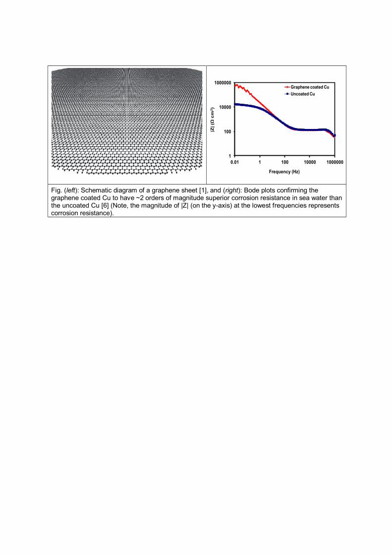
Fig. (left): Schematic diagram of a graphene sheet [1], and (right): Bode plots confirming the graphene coated Cu to have ~2 orders of magnitude superior corrosion resistance in sea water than the uncoated Cu [6] (Note, the magnitude of |Z| (on the y-axis) at the lowest frequencies represents corrosion resistance).
1
100
10000
1000000
0.01 1 100 10000 1000000
|Z| (
cm
2)
Frequency (Hz)
Graphene coated Cu
Uncoated Cu

Monte-Carlo simulation of the tight-binding model of graphene with
partially screened Coulomb interactions
Dominik Smith, Lorenz von Smekal
Theoriezentrum, Institut fur Kernphysik, TU Darmstadt,
Schloßgartenstraße 2, 64289 Darmstadt, Germany
Abstract
We present results of Hybrid-Monte-Carlo simulations based on the work of
Ref. [1] of the tight-binding theory of graphene, coupled to an electric two-bodypotential which is generated by a Hubbard-Stratonovich field [2, 3]. We have
investigated the spontaneous breaking of sub-lattice symmetry, which occurs
when the effective fine-structure constant αeff is large and which correspondsto a transition from a conducting to an insulating phase (Fig. 1). We chose
a form of the potential which correctly accounts for screening of the two-body
Coulomb interactions of valence-electrons by electrons in lower orbitals (Fig.2): At short range we used the exact results of the calculation within the con-
strained random phase approximation (cRPA) presented in Ref. [4]. At longrange we used a pheonomenological model to generate screening, which is
motivated by the same formalism. We compare our results to previous simula-
tions presented in Ref. [5], which correctly accounted for short-range screen-ing, but over-estimated screening at long distances. These authors located the
phase transition at αc ≈ 3.14. We find that sub-lattice symmetry-breaking is
largely insensitive to the exact form of the long-range part of the potential. Ourresults confirm the expectation that suspended graphene (αeff ≈ 2.2) is a con-
ductor, when screening is correctly accounted for.
References
[1] R. Brower, C. Rebbi and D. Schaich, “Hybrid Monte Carlo simulation
on the graphene hexagonal lattice,” PoS LATTICE 2011, 056 (2012)[arXiv:1204.5424]; [arXiv:1101.5131].
[2] D. Smith and L. von Smekal, “Monte-Carlo simulation of the tight-binding
model of graphene with partially screened Coulomb interactions,” in prepa-
ration.
[3] D. Smith and L. von Smekal, “Hybrid Monte-Carlo simulation of interacting
tight-binding model of graphene,” arXiv:1311.1130.
[4] T. O. Wehling et al., “Strength of effective Coulomb interactionsin graphene and graphite,” Phys. Rev. Lett. 106, 236805 (2011)
arXiv:1101.4007.
[5] M. V. Ulybyshev et al., “Monte-Carlo study of the semimetal-insulator
phase transition in monolayer graphene with realistic inter-electron inter-
action potential,” Phys. Rev. Lett. 111, 056801 (2013) arXiv:1304.3660.
1
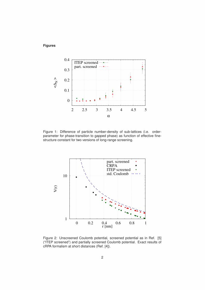
Figures
0
0.1
0.2
0.3
0.4
2 2.5 3 3.5 4 4.5 5
<∆
N >
α
ITEP screenedpart. screened
Figure 1: Difference of particle number-density of sub-lattices (i.e. order-parameter for phase-transition to gapped phase) as function of effective fine-
structure constant for two versions of long-range screening.
1
10
0 0.2 0.4 0.6 0.8 1
V(r
)
r [nm]
part. screenedCRPAITEP screenedstd. Coulomb
Figure 2: Unscreened Coulomb potential, screened potential as in Ref. [5]
(“ITEP screened”) and partially screened Coulomb potential. Exact results of
cRPA formalism at short distances (Ref. [4]).
2

Direct observation of sub-domains in the GO single layer
Narae Son
1,5, Hyunsoo Lee
2, Tae Gun Kim
3, Hu Young Jeong
4, Jong Yun Kim
1, Gyeongsook Bang
1,
Sehun Kim5, Jeong Young Park
2 and Sung-Yool Choi
1
Department of Electrical Engineering and Graphene Research Center, KAIST, 291 Daehak-ro, Daejeon,
Korea Graduate School of EEWS and KI for the Nanocentury, KAIST, 291 Daehak-ro, Daejeon, Korea
Korea Research Institute of Standards and Science, 267 Gajeong-ro, Daejeon 305-340, South Korea School of Mechanical & Advanced Materials Engineering and UNIST Central Research Facilities,
UNIST, 100 Banyeon-ri, Eonyang-eup, Ulsan, Korea Department of Chemistry and Molecular-Level Interface Research Center, KAIST, 291 Daehak-ro,
Daejeon, Korea [email protected] and [email protected]
Abstract
Chemically synthesized graphene oxide (GO) is an oxidized single graphitic monolayer that has
traditionally served as a precursor for graphene, but has a considerable potential of application for its
own characteristics. It has been experimentally proved that GO monolayer consists of randomly
distributed regions, aromatic regions (sp2 carbon atoms) and oxygenated aliphatic regions (sp
3 carbon
atoms) by raman spectroscopy [1], scanning tunneling microscopy (STM) [2] and high-resolution
transmission electron microscopy (HR-TEM) [3]. However, these methods have disadvantages such as
complicated and time-consuming preparation process and narrow region (a few nanometer) being
measured.
Here, we investigated the structural, chemical, and electrical properties of synthesized GO simple
by using a conductive atomic force measurement (C-AFM) analysis in a few micrometer range. GO
monolayer is composed of two different sub-domains, the first one corresponding to a high friction and
low conductance domain (sp3 carbon domain) and the other corresponding to a low friction and high
conductance domain (sp2 carbon domain) [4-5]. At each position of two domains, local I-V
characteristics also showed different behaviors depending on the chemical properties. To confirm
presence of sub-domains of GO, scanning transmission electron microscopy (STEM), HR-TEM analysis,
and oxygen electron energy loss spectroscopy (EELS) mapping were conducted.
References [1] C. Mattevi et al., Adv. Funct. Mater., 19 (2009) p. 2577.
[2] M. Ishigami, J. H. Chen, W. G. Cullen, M. S. Fuhrer and E. D. Williams, Nano Lett., 7 (2007) p. 1643.
[3] N. R. Wilson et al., ACS Nano, 3 (2009), p. 2547.
[4] J. H. Ko, S. Kwon, I. S. Byun, J. S. Choi, B. H. Park, Y. H. Kim and J. Y. Park, Tribol Lett., 50 (2013)
p. 137.
[5] S. Seo, C. Jin, Y. R. Jang, J. Lee, S. Kyu. Kim and H. Lee, J. Mater. Chem., 21 (2011) p. 5805.
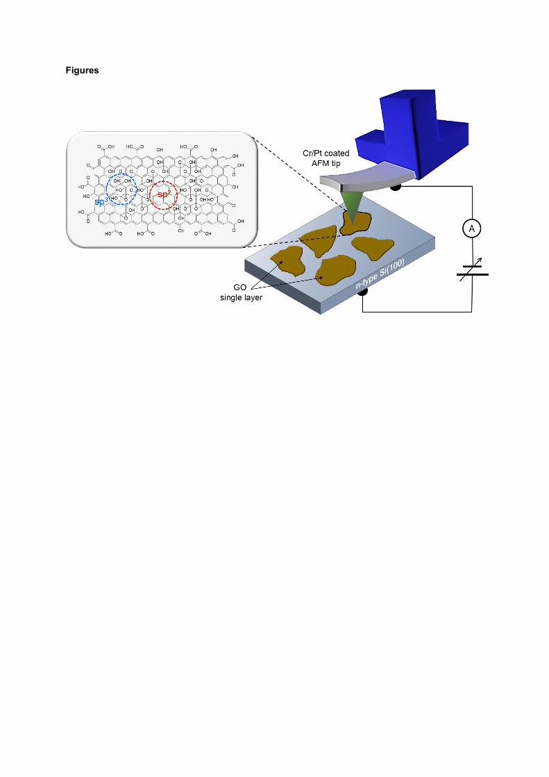
Figures

Humidity sensing characteristic of graphene oxide in low humidity
Young Jun Son, Ju Yeon Woo, Chang-Soo Han
School of Mechanical Engineering, Korea University, Seoul, 136-713, Korea
Abstract Graphene oxide has been known for its advantage for sensing water molecules. There are several
papers about using graphene oxide as humidity sensor.[1],[2]
Graphene oxide shows very fast response and recovery time, and excellent sensitivity. But humidity sensing behavior of graphene oxide in low humidity environment is not yet described. Here, we tested humidity sensing characteristic of graphene oxide, especially in low humidity environment. Electrodes were deposited on substrate by E-beam evaporation and graphene oxide membranes were made by vacuum filtration and stamped on the substrate. We measured resistance between two electrodes with changing humidity environment. When graphene oxide was exposed less than 30% relative humidity, the resistance of graphene oxide increased almost exponentially and finally the resistivity went extremely high. In this presentation, we explain the main mechanism of this reason and suggest the compensating method to sense the low humidity. References [1] Hengchang Bi, Kuibo Yin, Xiao Xie, Jing Ji, Shu Wan, Litao Sun, Mauricio Terrones and Mildred S.
Dresselhaus, Scientific reports, 3(2013), 2714.
[2] Stefano Borini, Richard White, Di Wei, Michael Astley, Samiul Haque, Elisabetta Spigone, Nadine Harris, Jani Kivioja, and Tapani Ryhanen, ACS nano, 12(2013), 11166-11173.

Contribution (Poster)
Work function shifts of monolayer and few layers of graphene under metal electrodes
Seung Min Song, Jae Hoon Bong, and Byung Jin Cho
Department of Electrical Engineering, KAIST, 291 Daehak-Ro, Yuseong-gu, Daejeon 305-701, Korea [email protected]
Due to the exceptionally ultimate properties of graphene, it is expected to be utilized for the various
electronic applications including flexible and transparent electrodes, high transport channel materials,
photo- or bio-sensitive detectors and so on.[1] Most of those devices inevitably need metal contact to
graphene in order to measure the electronic characteristics or supply energy to operate. The properties
of contact between graphene and metal is therefore one of the crucial factors determining the device
performances. In terms of the device engineering, work function of material is fundamental information
to tailor the device characteristics. Even though there have been a few of results related to work
function of the exposed graphene, a research on work function change of graphene under metal is rare
and the systematic study is required. Here, we report the work function shift of graphene under metal
by measuring capacitance-voltage of metal-graphene-oxide-silicon capacitors. To verify the work
function shift of monolayer graphene under various metal species, four deferent metals of Cr/Au, Ni, Au
and Pd were formed on graphene. In contrast to the high work function of the bare graphene of
4.89~5.16 eV,[2] metal contacted graphene is found to have different work function and it shows metal
dependency. The work function of graphene under Cr/Au or Ni coincides with the corresponding metals
but it is found to be pinned to be a certain value for the Pd or Au contact. The work function shift of
multi-layer graphene was also investigated with Cr/Au contact. Monolayer graphene was transferred
repeatedly to form 2~4 layers of graphene. Interestingly, the influence of metal is found to decrease
with the number of graphene layers. These results are believed to give important clues for the
development of the advanced graphene devices and the understanding of the deeper analysis.
This work was supported by a National Research Foundation of Korea (NRF) research grant (2010-
0029132, and 2011-0031638).

Contribution (Poster) References [1] K. S. Novoselov, V. I. Falko, L. Colombo, P. R. Gellert, M. G. Schwab, and K. Kim, Nature 490 (2012) 192-200. [2] J. K. Park, S. M. Song, J. H. Mun, and B. J. Cho, Nano Letters 11 (2011) 5383-5386. Figures
-3 -2 -1 0 1
0.0
0.2
0.4
0.6
0.8
1.0
1.2
VG [V]
5002
m2
1 layer
2 layers
3 layers
4 layers
w/o gr
No
rma
lize
d C
G
graphenemetal
SiO2
Si
Vg
g
(a) (b)
Figure 1. (a) Illustration of metal-graphene-oxide-silicon capacitors with four layers of graphene. (b) The capacitance-voltage measurement result of the capacitors with different number of graphene layers when metal fully covers the graphene.

CVD graphene growth on non-planar surfaces, a pilot investigation
Adam C. Stoot, Alexander B. Christiansen, Martin B.B.S. Larsen, P. Bøggild
DTU Nanotech, Department of Micro- and Nanotechnology, Kgs. Lyngby, Denmarke-mail: [email protected]
AbstractGraphene has attracted a lot of attention due to its unique optical, electronic and mechanical properties, promising transparent, flexible, faster electronics as well as the possibility of making completely new kinds of devices [1, 2]. Moreover, graphene’s impermeability makes it a strong candidate for new types of advanced anticorrosive coatings [3]. As the process of growing graphene on planar catalysts (e.g. Cu or Ni) is becoming well understood new challenges arise growing graphene on industrial, 3-dimensional rough non-clean samples or in processes were the catalyst shape is used for graphene band gapengineering.
One first step to overcome these challenges, and be able to grow graphene on different substrates for instance cheaper catalysts, is to investigate the effect of surface roughness of the catalyst material. Previous work has demonstrated growth of graphene on some nanostructures [4]. Here we present a pilot study investigating the roughness limits for graphene growth on nickel. Different grades of roughness were fabricated using clean room techniques and black silicon reactive ion etching [5] to create these surfaces. These substrates were covered by a nickel film and the wafers etched away to leave behind a pure nickel slab with the desired surface morphology. An Aixtron Black Magic chemical vapour deposition (CVD) system was used for the growth of graphene. Subsequently the samples were investigated using optical microscopy (OM), scanning electron microscopy (SEM) and micro Raman spectroscopy mapping [6].
Raman spectroscopy gives indications of a roughness limit for graphene growth on a nickel catalyst and thus reveals some of the challenges of making graphene a part of a viable coating solution.
References
[1] M. Katsnelson, MaterialsToday, jan-Feb (2007), page 20-27[2] A.K Geim and K.S. Novoselov, Nature Materials, (2007), page 183-191[3] D. Prasai, ACS Nano, 6 (2) (2012), page 1102-1108[4] X. Li et al., Nature Scientific Reports, 2 (2012), article 395[5] H. Jansen, Micromech. Microeng. 5 115 (1995), page 115-120[6] A.C. Ferrari et al., Physical Review Letters, (2006)
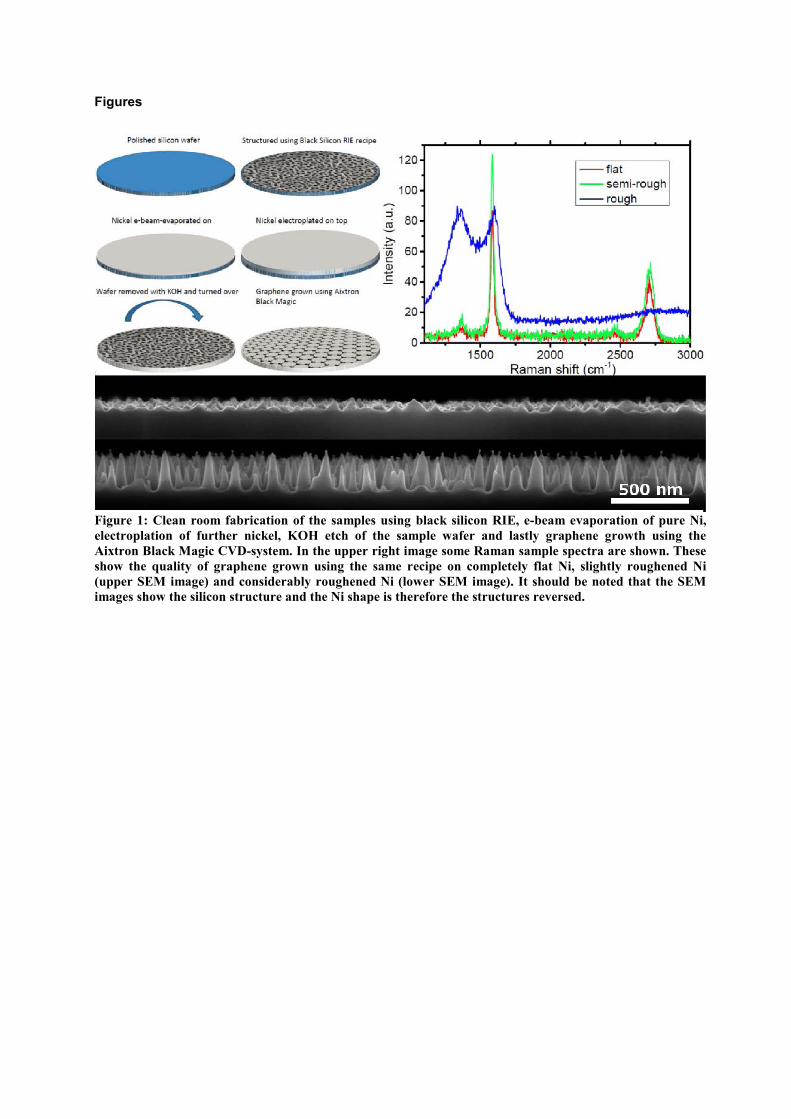
Figures
Figure 1: Clean room fabrication of the samples using black silicon RIE, e-beam evaporation of pure Ni,
electroplation of further nickel, KOH etch of the sample wafer and lastly graphene growth using the
Aixtron Black Magic CVD-system. In the upper right image some Raman sample spectra are shown. These
show the quality of graphene grown using the same recipe on completely flat Ni, slightly roughened Ni
(upper SEM image) and considerably roughened Ni (lower SEM image). It should be noted that the SEM
images show the silicon structure and the Ni shape is therefore the structures reversed.
Graphene Toulouse 2014 2/11/2014 4:57:40 PM
Low-Cost High-Volume Scale Up of CVD Graphene
Karlheinz Strobl, Mathieu Monville, Riju Singhal, Samuel Wright, and Leonard Rosenbaum
CVD Equipment Corporation, 355 S. Technology Drive, Central Islip, New York 11722, USA Email: [email protected] CVD graphene can be manufactured on copper substrates using chemical vapour deposition (CVD) based processing. CVD graphene manufacturing process recipes are typically first developed and optimized on either atmospheric or low pressure R&D tube furnace systems. For these tools, the width and/or length of the CVD graphene growth substrate is traditionally limited by the diameter and heating length of a given process tube. Therefore, the general thinking is that only roll to roll CVD systems are able to mass produce CVD graphene.
Transferring an R&D CVD graphene growth process to a roll to roll CVD system can be time consuming, capital intensive, and potentially needs a lot of process redevelopment. Roll to roll CVD processing equipment is very customized, expensive to design and manufacture, and limits the available processing window. This can make the scaling up of CVD graphene production a risky effort, thereby holding back commercialization of CVD graphene enabled products.
We present test results of CVD graphene manufactured using a novel reactor design family1
that allows for high quality, uniform deposition with a significant increase in CVD graphene substrate size as compared to the standard R&D CVD reactor setup. Process transfer and scale-up from R&D to production quantities is quick and straightforward. We demonstrate that our CVD reactors have the potential to outperform roll to roll systems in terms of throughput, while still retaining high quality material properties and characteristics. The cost per coated area is significantly reduced as compared to a roll to roll system. We will also demonstrate that this technology allows for the production of large rolls of graphene-coated flexible catalyst substrates that can be integrated into any roll to roll post-processing for various applications such as sensors, flexible transparent conductors, nanoporous membranes, photovoltaics, etc.
In summary, we present an accelerated, lower risk and lower cost route to the scale up manufacturing of CVD graphene on both sheets and rolls of copper foil, whether manufactured with low pressure or atmospheric pressure CVD systems.
References
1Scalable 2D-FILM CVD Synthesis, patent pending

Contribution (Oral/Poster/Keynote)
The Electrical Properties of Fluorinated Graphene and its Application in Graphene-based Nanoelectronics
Kuan-I Ho1, Jia-Hong Liao1, Chao-Sung Lai 1, Ching-Yuan Su 2*
1Department of Electronic Engineering, Chang Gung University, Tao-Yuan 333, Taiwan
2Graduate Institute of Energy Engineering, National Central University, Tao-Yuan 32001 , Taiwan
* Corresponding author: [email protected]
Fluorinated graphene, the so-called fluorographene (F-Graphene),[1-3] exhibits a comparable
mechanical strength to pristine graphene, while the conductivity can be adjusted from a semi-metallic
character to insulator by tuning the stoichiometry, i.e., adjusting the carbon-to-fluorine ratio (C/F).[2] The
theoretical calculation predicts that partial fluorination of graphene from C32F to C4F is able to modify the
energy bandgap from 0.8 to 2.9 eV, respectively. As a result, fluorographene is a promising candidate to
be used in next-generation nanoeletronics.
To develop a transistor, it requires three types of materials: (a) the highly conducting materials
for use in electrode and interconnection,(b) semiconducting materials for the formation of active area,
and (c) insulator for isolation between devices and gate electrode. The traditional technique relies on
the patterning and deposition of these three types of materials with stacking layered configuration. Now,
the transistor could be fabricated on an atomic-layered material by selective functionalization of
graphene with fluorine. The electrical properties of fluorinated graphene can be adjusted from
conductive to insulator depends on the coverage and types of C-F bond formation. In this work, the
wafer scale fabrication of atomic layered transistors are demonstrated by selective fluorination of
graphene with a remote CF4 plasma, where the generated F-radicals preferentially fluorinated graphene
surface at low temperature (<200oC) while this technique lower the defect formation by screening out
the ion damage effect. The resultant grapehene shows electrical semiconducting and isolation after
subjected to the fluorination for 5~20min, respectively(Figure 1a). A back-gate transistor is then
fabricated with a fluorination of graphene film on SiO2 substrate. The chemical structure, C-F bonds, is
well correlated to the electrical properties in fluorinated graphene by XPS, Raman spectroscopy and
electrical meter. This efficient method provide electrical semiconducting and insulator of graphene with a
large area and selective pattering, where it turns out the potential for the integration of electronics down
to atomic layered scale.
Moreover, the graphene-based transistor was demonstrated with a vertically stacked
architecture. To fabricate graphene-based field effect transistor, depositing gate dielectric with high
quality and uniformity is required. In this work, the Fluorinated multilayer graphene film was applied as
the gate dielectric layer in a graphene-based FET(Figure 1b). It was found out that extremely thin
fluorographene (~5nm) exhibit a high breakdown electric field (above 10MV cm-1) and high thermal
stability. The present method is simple and scalable, which shows the potential to be used in the
fabrication of next-generation of nano-electronics.
.
References
[1] R. R. Nair, W. Ren, R. Jalil, I. Riaz, V. G. Kravets, L. Britnell, P. Blake, F. Schedin, A. S. Mayorov, S.
Yuan, M. I. Katsnelson, H.-M. Cheng, W. Strupinski, L. G. Bulusheva, A. V. Okotrub, I. V. Grigorieva, A.
N. Grigorenko, K. S. Novoselov, A. K. Geim, Small 2010, 6, 2877.

Contribution (Oral/Poster/Keynote)
[2] J. T. Robinson, J. S. Burgess, C. E. Junkermeier, S. C. Badescu, T. L. Reinecke, F. K. Perkins, M. K.
Zalalutdniov, J. W. Baldwin, J. C. Culbertson, P. E. Sheehan, E. S. Snow, Nano Letters 2010, 10, 3001.
[3]S. Kwon, J.-H. Ko, K.-J. Jeon, Y.-H. Kim, J. Y. Park, Nano Letters 2012, 12, 6043.
Figure1. (a) The sheet resistance for the F-Graphene samples with different exposure times. (b) An illustration of a
graphene-based FET composed of a fluorographene gate dielectric.
VUV-induced reduction of graphene oxide in two-dimensional pattern arrays with sub-µm resolution
Hiroyuki Sugimura1, Y. Tu
1, T. Ichii
1, O. P. Khatri
2
1Department of Materials Science and Engineering, Kyoto University, Sakyo, Kyoto 606-8501, Japan
2Chemical Science Division, CSIR-Indian Institute of Petroleum, Dehradun - 248005, India
Graphene oxide (GO), which is a derivative of graphene decorated with polar functional groups such as hydroxyl, carbonyl, carboxyl and epoxy groups [1]. Chemical processing, in which graphite is oxidized to some extent, has been applied to produce GO [2, 3] and accepted as a promising method as the mass-scale production of graphene-based materials, among all known approaches like micromechanical exfoliation of graphite, chemical vapor deposition, epitaxial growth, etc.[4]. Due to the hydrophilic nature of GO, it can be dispersed in a polar solvent, even in water, consequently, GO thin films can be readily formed on any types of solid substrates by simply casting from an aqueous solution of GO nanosheets. However, GO is distorted in electronic properties compared with graphene, since oxidized parts in GO are much less conductive than the sp
2 network in graphene. The elimination of
oxygen functionalities and recovering of the -conjugated network are, thus, very important in order to restore the graphene characteristics. The reduction of GO is an approach to increase conductivity of GO. Reduced GO (rGO), which is a reduced from of GO at least partially, show resemble characteristics to graphene. Actually, electronic conductivites were reported to be recovered when GO was reduced to rGO [5]. The rGO can be prepared via thermal annealing or chemical reduction using strong reducing agents like hydrazine hydrate [5]. Although these processes are certainly effective, there have been some disadvantages, that is, large energy consumption or the use of toxic reagent, unfavorable for industrial applications. In order to overcome such problems, a variety of approaches based on photo-chemical, -catalytical or -thermal reduction, which are performable around room temperature have been reported so far [6-8]. However, further studies to develop a new reduction process are still necessary to fulfill requirements to adopt rGO to microelectronic devices. Here we propose another approach to reduce GO to rGO by the use of vacuum ultra-violet (VUV) light. This idea is based on VUV-decomposition of poly(methyl methacrylate) (PMMA) resin. In our previous research, we found that oxygen-containing parts of PMMA was decomposed when irradiated with a VUV light at 172 nm wavelength [9]. We have expected that oxidized parts of GO could be trimmed similarly. GO nanosheets with a size of 20-50 µm were prepared by a modified Hummers’ method [3]. The aqueous GO solution was spin-casted onto a highly-doped Si substrate covered with a surface oxide layer of 90 nm in thickness. The GO-based substrate was located in a vacuum chamber. After evacuated below 10
-3 Pa, VUV light was irradiated to the sample surface for 15 min. A Xe excimer lamp
(Ushio Inc., radiating wavelength and intensity: 172 nm and 10 mWcm-2
) was used for the VUV light source. Figure 1 shows C1s-XPS profiles of GO and VUV-irradiated GO. Due to VUV-irradiation, the peak intensity around 287-288 eV corresponding to photoelectrons from C atoms bonded with O with a form of C-O, C=O, od COO decreased. On the contrary, the peak intensity around 285 eV corresponding to those form the sp
2 graphene network increased with the VUV-irradiation. This result
means that GO is certainly reduced to rGO and the -conjugated network is recovered by the VUV-irradiation in vacuum. Figure 2 shows topographic and surface potential images of GO and rGO-VUV acquired by Kelvin-probe force microscopy (KFM). Both GO and rGO sheets show a topgraphic height about 1 nm. However, the surface potential of GO is 50 mV higher than that of the SiO2/Si substrate, while the potential of rGO-VUV is 30 mV lower than the substrate. Although the origin of these surface potential contrasts are still under investigation, KFM is proved to be a powerful means to probe a state of GO (oxidized or reduced) locally. Next, another GO-casted sample in vacuum was irradiated with VUV light for 2 min with the same procedure except that a photomask (Cr patterns formed on a quartz plate) was placed on the sample. Figure 3 shows optical, topographic and surface potential images of GO sheets with the patterned VUV-irradiation through the photomask. As clearly indicated in the optical micrographs, the VUV-irradiated regions (rGO-VUV) are seen as dark compared with the un-irradiated regions (GO). In the surface potential images, the VUV-irradiated regions (rGO) show lower surface potentials in accordance with the results shown in Fig. 3. In addition, from the close inspection of the topographic images, the rGO-VUV regions are confirmed to be depressed about 0.2 µm in depth. In conclusion, the VUV-irradiation to GO in vacuum has been found effective to reduce GO to rGO probably through the selective trimming of oxygen containing parts in GO. This chemical change could be visible by KFM. Moreover, we have succeeded in fabricating rGO patterns with a spatial resolution of

0.5 µm on GO. This method is useful for GO/rGO based microelectronics and its extension to a wafer-scale production will be possible.
References[1] D. R. Dreyer, S. Park, C. W. Bielawski, R. S. Ruoff, Chem. Soc. Rev. 39 (2010) 228. [2] W. S. Hummers and R. E. Offeman, J. Am. Chem. Soc. 80 (1958) 1339. [3] M. Hirata, T. Gotou, S. Horiuchi, M. Fujiwara and M. Ohba, Carbon, 42 (2004) 2929. [4] M. J. Allen, V. C. Tung and R. B. Kaner, Chem. Rev. 110 (2010) 132. [5] C. K. Chua, M. Puram, Chem. Soc. Rev. 43 (2014) 291. [6]Y. Zhou, Q. Bao, B. Varghese, L. A. L. Tang, C. K. Tan, C.-H. Sow and K. P. Loh, Adv. Mater. 22(2010) 67. [7] Y. Matsumoto, M. Koinuma, S. Y. Kim, Y. Watanabe, T. Taniguchi, K. Hatakeyama, H. Tateishi and S. Ida, ACS Appl. Mater. Interf. 2 (2010) 3461. [8] S. Prezioso, F. Perrozzi, M. Donarelli, F. Bisti, S. Santucci, L. Palladino, M. Nardone, E. Treossi, V. Palermo, and L. Ottaviano, Langmuir 28 (2012) 5489. [9] A. Hozumi, T. Masuda, K. Hayashi, H. Sugimura, O. Takai, and T. Kameyama, Langmuir 18 (2001) 9022.
Figures

��������������������� ������������ �������������������������������
����������������������� �� ��
������������������������������������������������������������ ���������������!�"�������������������#������$�����%�����������&�����'())'*��%��
�%���������$������+� ,,�-����������
��������
���"����$��������� �������������.������������������/�������� ���������$������������"�$�����0������1������/������,������������"���������$��2������$�����%���� ���������$�,������ ���������$3��.������������������!��������$�$���"������������������������������� ����� ����� ��������������� � �����0����������� ������ �������������� ��������������4���������������,���������� �5���������$�����������5���������#�4���$� ���� ��������� �5���������$�������$�����$������������������������������� �������,��������$��$�����������"������������������������.���������������������������������������� �����������$�����������������5��������6�� � �������������������������������������������������������"����$��������������,���6�$��7����,�"��������������,���� ��,��� �5���������$������������ � ��� ���� � ������,����� ������������ � ��� ����������� ���������������������������������#�$������,���������� ���%���� ���������$���������� �6�� �������������������������� ��������������������������������������������������������������������������"������������� ���������� �������������,���������&�$������������"����$������������������� �,����� �"��"������� ������$������ ������������ �������� ��������������������� ���������$� ���,�"����,�����������&�$������������"��"�$��������������������������,������������������ ���������� ���������������,��������� �5���������$�������,������,���6�$��'�� � ���� � �"����$�� � ��� ��� ��� ��� � ��� �������� ����� � ��� ������� � 8� � �� � ���, � ��� � ��� � �� �����
�"������� � �� � ��� � ������"� � ���������� � ��� ����� � ������ � ��� � ��� � ��������� � $��� � ,��� � �����.���� ������� $������� �97:������ ������� �9':�"����,�����,�����,������������������������ ���������.��������������26�$��(3��6����������,�����.������,�����,���������������������������������� �������5��������� ��4�������������,������� ���������������������,�������������������8 ������� � �� � ����������"� ����������� � ��� ������ � �����$��"���� �,������ ����� ����� � ����
�������� ����������6�� ��������������9(�;�<:���������"����$�����8��������,������������������$���������� ��$��"� ����������� � ��� ����� �� ����� �� � ��, ������5����� ����$� � 2� � ��� ������ ��� � �����������$����3 ��� �� ���$�����$��2 ���� ��$�� � ��������������$����3� �6�� � ���� ��,������5���������$������������$��"���������������� ������������������� ����� ��������������������������������"�����������������$��"���������������������������������������� ��$��&������������$�������5���������$������������$��"������������� ��� ������������,����������������,�����������5���������� �����������$����������������/�������� ������������� ��������������$���������� ��/�������� �������������������� ������������������������5���������$��� ���������,�����������$��"���������������� ���������� ����� ��������������5��������������� ��������������������"���� � =��������� � ��� � ��� � ������ � �� ����� � ��� � ���������� � �� � ��� � �$��"� � �������������� ������������,������ ����� ����������������56��0�����5���$���������������$�#��� �,��0 �,� � ��������� ��� � ��� ������ � 1��� �>������ ����$� ��� �%�� � ���� �?�� �����
')7'%1@''))'�������������������������6����������%��������?�������7)A'<;7A������������$�� � �������� � >������ � ���$� � �� � ��� � %����� � &��� � � �� � ������� � ���� � ?�� � ����B�1)7))))))�
����������
97:���� $��C���������������&��?���$���������"� ��D��1��������������%������0����C���,$��6��>�����?����������%�����>��45D�$������C����0��&�������������������2')7)3��)E7@7A�
9':����C���������������������C����$������� �������������=���������������>�"��1� !2')773��7'7;);2>3�
9(:�C����$����������%��%�$��C�����#��������?��?��?��4����&������������������"2')7)3��7*(7)(�9;:�C����$��#������C��������?��?��?��4����&%�����#2')773��('AE�9<:����1�����$�����F�����#�� �4����=��������6��������������"�����C�����>����%��>�������&��F�������#��=���������������>�"��1� !2')773��7<(;7)�
9*:�1����������������������� �� ���������>�"��1� #2')7'3�7'<;7(�9A:�1������������� �� �����,�C��������$#2')7(3��)E()(E�9E:�1������������� �� ���������>�"��1� 2')7(3�'(<;''�
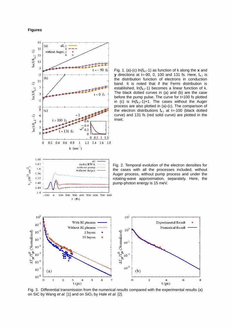
%������
6�$��7��2352�3��2�&�7573�������������0���$����������� �������������G5@)��)��7))���7(7������������&�7� ������ � ����������� � ������� �� � �������� � � � ������������ � 8� � �� � ���� � ��� � �� � ��� � 6�� � � ����������� � ����������������2�&�7573� ���� �������������������0��#������0�����������"�����23���2�3������������������������� ���������#������"�������G7))������������� � 2�3 � �� � �2�&�7573H7� � #�� � ���� � ,������ � ��� �&�$����������������������������2352�3��#����� ���������������������������������� �&�7� � � �G57))�2���0�����������"�3���7(7����2�������������"�3������������������������
�
6�$��'��#� ������"�������������������������������������� � ���� � ,��� � �� � ��� � ��������� � �������� � ,�������&�$������������,��������� ��������������������������$5,"� � ����.� ���� � ��������� � ����� � ������ �5���������$�����7<� �D�
6�$��(����������������� ��������� ������ ���������������� �����,���������.���� ������������23�����%���� $��������97:�������I'���������������9':��

Charge tuning of non-resonant magneto-exciton phonon interactions in graphene
Anna K Swan, Sebastian Remi, Bennett Goldberg Boston University, , Boston MA 02215
Abstract
We explore the interactions between the G-band phonon and Landau level (LL) excitons far from energy resonance in graphene[1]. In a strong perpendicular magnetic field, the graphene electron energy bands split into discrete Landau levels. It has been shown earlier that when the G-band phonon energy overlaps with a LL exciton energy, the phonon and LL exciton can mix via electron-phonon coupling, and the interaction on resonance is well described by a single 2 level coupled mode description[2]. Anti-crossings at resonance have been observed by magneto Raman spectroscopy of decoupled surface layers of graphene on graphite [3-and more recently on exfoliated graphene on SiO2 [6] Here we show for the first time charge carrier density dependent magneto Raman measurements on single layer graphene field effect devices at constant magnetic fields. Contrary to previous magneto-phonon studies, we explore the Raman response in a magnetic field far from magneto-phonon resonance conditions. We demonstrate a linear dependence on the phonon frequency with the LL filling,
, for the non-resonant regime, rather than the behavior predicted for the on-resonance response. Notably, at a constant magnetic field, we observe pronounced splittings and slope changes of the G-
band phonon energy as a function of . The coupling of the G-band phonon to magneto-excitons in single layer graphene displays kinks and splittings versus filling factor that are well described by Pauli blocking and unblocking of inter- and intra- Landau level transitions. In order to model this dependence, we linearize the equation for the phonon shift as a function of magnetic field and charge density. We use values of the Fermi velocity and the electron-phonon coupling strength from zero magnetic field measurements of the phonon energy shifts due to electronic screening by charge carriers, Fig 1. We observe signatures of the logarithmic divergence of the phonon energy as a function of the charge carrier density at liquid He temperatures after vacuum annealing on single layers. Fig 1 (a). The fit of the measured dependence on charge density yields the values of the
electron-phonon coupling strength, , and the Fermi velocity vF. These values form zero magnetic field is then used, without further fitting, in the linear model to predict the dependence of the phonon energy in a magnetic field as function of the charge density, as is shown in fig 2c). The qualitative and quantitative agreement between spectra and a linearized model of electron-phonon interactions in magnetic fields is shown. The reason for the kinks in the phonon energy is understood by considering the effect of filling and emptying LL, and hence blocking or turning on different symmetry allowed transitions. This is illustrated in Fig 2 (a) and (b). Fig 2 (a) shows the dependence on circular polarization of the incident laser light. In
this example, the n=0 LL is fully filled, which blocks the - transitions between n=-1 to 0, and for all
lower n s. On the other hand, the equivalent + transition from n=0 to 1 is fully on. The effect on the
phonon energy for the different + transitions as a function of filling is shown in Fig 2 (b). The splitting of the Raman G band is caused by dichroism of left and right handed circular polarized light due to lifting of the G-band phonon degeneracy, as illustrated in Fig 2 a). The piecewise linear slopes are caused by
the linear occupancy of sequential Landau levels. Fig 2 b) illustrates the dependence of on the different resonances. This is in contrast to earlier work on-resonance, where the Landau level filling
dependence is proportional to . In contrast to on-resonance measurements, no single transition dominates the coupling, and several inter and intra-band transitions have to be considered to account for the experimental observations. By focusing on the non-resonant regime we have discovered fine structure in the G-band optical phonon in single layer graphene at high magnetic fields as a function of charge density. The observed behavior is caused by coupling between the phonon and magneto-exciton far from resonance that result in a linear dependence on filling factor, in contrast to on-resonant coupling that leads to a square root dependence on filling factor.
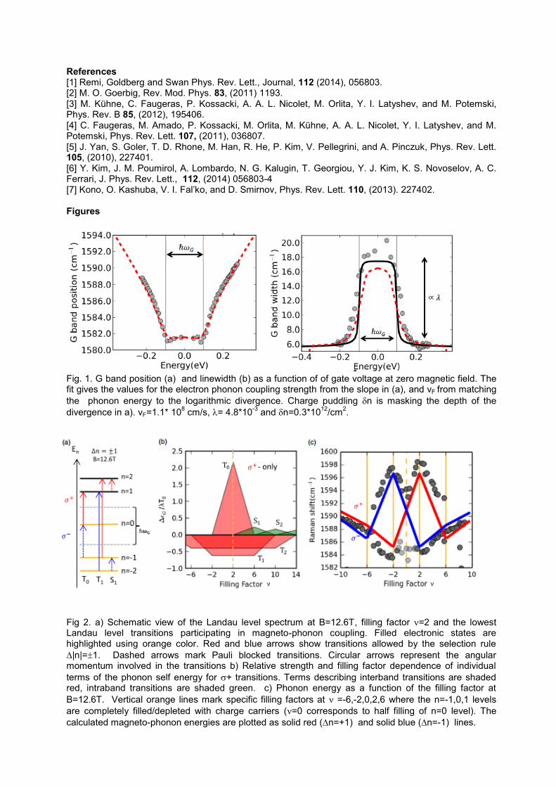
References [1] Remi, Goldberg and Swan Phys. Rev. Lett., Journal, 112 (2014), 056803. [2] M. O. Goerbig, Rev. Mod. Phys. 83, (2011) 1193. [3] M. Kühne, C. Faugeras, P. Kossacki, A. A. L. Nicolet, M. Orlita, Y. I. Latyshev, and M. Potemski, Phys. Rev. B 85, (2012), 195406. [4] C. Faugeras, M. Amado, P. Kossacki, M. Orlita, M. Kühne, A. A. L. Nicolet, Y. I. Latyshev, and M. Potemski, Phys. Rev. Lett. 107, (2011), 036807. [5] J. Yan, S. Goler, T. D. Rhone, M. Han, R. He, P. Kim, V. Pellegrini, and A. Pinczuk, Phys. Rev. Lett. 105, (2010), 227401. [6] Y. Kim, J. M. Poumirol, A. Lombardo, N. G. Kalugin, T. Georgiou, Y. J. Kim, K. S. Novoselov, A. C. Ferrari, J. Phys. Rev. Lett., 112, (2014) 056803-4 [7] Lett. 110, (2013). 227402. Figures
Fig. 1. G band position (a) and linewidth (b) as a function of of gate voltage at zero magnetic field. The fit gives the values for the electron phonon coupling strength from the slope in (a), and vF from matching
the phonon energy to the logarithmic divergence. Charge puddling n is masking the depth of the
divergence in a). vF=1.1* 108 cm/s, = 4.8*10
-3 and n=0.3*10
12/cm
2.
Fig 2. a) Schematic view of the Landau level spectrum at B=12.6T, filling factor =2 and the lowest Landau level transitions participating in magneto-phonon coupling. Filled electronic states are highlighted using orange color. Red and blue arrows show transitions allowed by the selection rule
|n|= 1. Dashed arrows mark Pauli blocked transitions. Circular arrows represent the angular momentum involved in the transitions b) Relative strength and filling factor dependence of individual
terms of the phonon self energy for + transitions. Terms describing interband transitions are shaded red, intraband transitions are shaded green. c) Phonon energy as a function of the filling factor at
B=12.6T. Vertical orange lines mark specific filling factors at =-6,-2,0,2,6 where the n=-1,0,1 levels
are completely filled/depleted with charge carriers ( =0 corresponds to half filling of n=0 level). The
calculated magneto-phonon energies are plotted as solid red ( n=+1) and solid blue ( n=-1) lines.
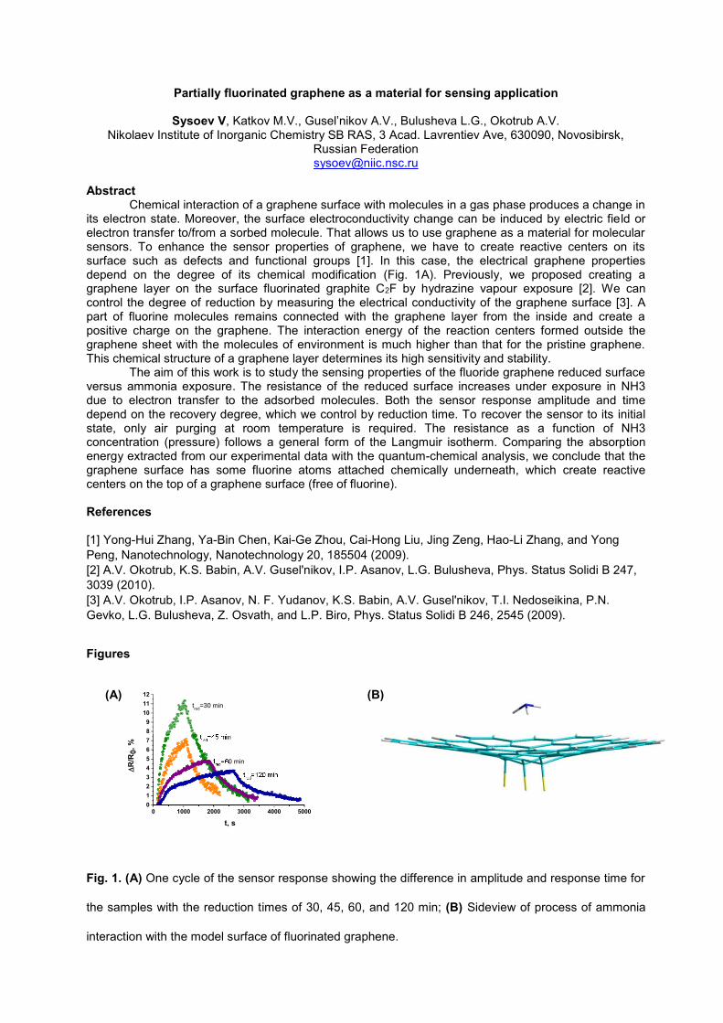
Partially fluorinated graphene as a material for sensing application
Sysoev V, Nikolaev Institute of Inorganic Chemistry SB RAS, 3 Acad. Lavrentiev Ave, 630090, Novosibirsk,
Russian Federation [email protected]
Abstract
Chemical interaction of a graphene surface with molecules in a gas phase produces a change in its electron state. Moreover, the surface electroconductivity change can be induced by electric field or electron transfer to/from a sorbed molecule. That allows us to use graphene as a material for molecular sensors. To enhance the sensor properties of graphene, we have to create reactive centers on its surface such as defects and functional groups [1]. In this case, the electrical graphene properties depend on the degree of its chemical modification (Fig. 1A). Previously, we proposed creating a graphene layer on the surface fluorinated graphite C2F by hydrazine vapour exposure [2]. We can control the degree of reduction by measuring the electrical conductivity of the graphene surface [3]. A part of fluorine molecules remains connected with the graphene layer from the inside and create a positive charge on the graphene. The interaction energy of the reaction centers formed outside the graphene sheet with the molecules of environment is much higher than that for the pristine graphene. This chemical structure of a graphene layer determines its high sensitivity and stability.
The aim of this work is to study the sensing properties of the fluoride graphene reduced surface versus ammonia exposure. The resistance of the reduced surface increases under exposure in NH3 due to electron transfer to the adsorbed molecules. Both the sensor response amplitude and time depend on the recovery degree, which we control by reduction time. To recover the sensor to its initial state, only air purging at room temperature is required. The resistance as a function of NH3 concentration (pressure) follows a general form of the Langmuir isotherm. Comparing the absorption energy extracted from our experimental data with the quantum-chemical analysis, we conclude that the graphene surface has some fluorine atoms attached chemically underneath, which create reactive centers on the top of a graphene surface (free of fluorine). References [1] Yong-Hui Zhang, Ya-Bin Chen, Kai-Ge Zhou, Cai-Hong Liu, Jing Zeng, Hao-Li Zhang, and Yong
Peng, Nanotechnology, Nanotechnology 20, 185504 (2009).
[2] A.V. Okotrub, K.S. Babin, A.V. Gusel'nikov, I.P. Asanov, L.G. Bulusheva, Phys. Status Solidi B 247,
3039 (2010).
[3] A.V. Okotrub, I.P. Asanov, N. F. Yudanov, K.S. Babin, A.V. Gusel'nikov, T.I. Nedoseikina, P.N.
Gevko, L.G. Bulusheva, Z. Osvath, and L.P. Biro, Phys. Status Solidi B 246, 2545 (2009).
Figures
Fig. 1. (A) One cycle of the sensor response showing the difference in amplitude and response time for
the samples with the reduction times of 30, 45, 60, and 120 min; (B) Sideview of process of ammonia
interaction with the model surface of fluorinated graphene.
(A)
0 1000 2000 3000 4000 50000
1
2
3
4
5
6
7
8
9
10
11
12
tred
=120 min
tred
=60 min
tred
=45 min
tred
=30 min
R/R
0, %
t, s
(B)

Quantum Transport in Deformed Graphene via Dirac Equation in Curved Space
Nikodem Szpak
Faculty of Physics, University Duisburg-Essen, Lotharstr. 1, 47057,Duisburg, Germany
As is well-known, low energy excitations in graphene can be effectively described by the 2-dimensional
Dirac equation. A natural question arises, to what extent (elasitically) deformed graphene can be
described by a version of the Dirac equation in a curved 2D-space. This analogy would enable for an
effective treatment of diverse local and global (topological) modifications of regular graphene sheets
and calculations of their transport properties.
We address this question in more detail, explain the effective continuous picture and point out some
difficulties appearing in the geometric interpretation of various terms (in particular, between the pseudo-
of electric currents in presence of a localized bump.
References [1] N. Szpak, A sheet of graphene quantum field in a discrete curved space
Figures
Energy structure of graphene quantum dots with edge relaxation
Wroc aw University of Technology, Wybrze e Wyspia skiego 27, Wroc aw, Poland
The effect of e quantum dots (GQDs) [1,2] and graphene nanoribbons (GNRs) [3-6]. The process of the edge relaxation affecting the band structures of GQDs and GNRs is studied. We investigate nanostructures of different shapes (hexagonal and triangular), sizes, and edge types (armchair and zigzag). For small systems, a comparison is made of simple tight-binding (TB) model to the case of the nanostructure geometry optimized within density functional theory (DFT) methods [7]. A change of the bond length between the atoms located at the edges produces variable hopping integral. We express hopping energy as a function of atomic distance in terms of Chebyshev polynomials [8]. We show that increasing with the lattice distance, hopping term accounts for the larger energy gap. An influence of hopping values variations on edge states in nanostructures with zigzag edges is investigated. We analyze the effect of hopping changes on the energy spectrum in a wide range of the hopping energies [8]. Our studies allow us to derive accurate TB model in order to investigate electronic properties of graphene nanostructures of sizes not accessible within DFT methods.
References
[1] S. Okada, A. Oshiyama, Phys. Rev. Lett. 87 (2001), 146803.
[2] H. Zheng, W. Duley, Phys. Rev. B 78 (2008), 45421.
[3] Y.W. Son, M.L Cohen, S.G. Louie, Nature 444 (2006), 347.
[4] T. Kawai, Y. Miyamoto, O. Sugino, Y. Koga, Phys Rev. B 62 (2000), 16349.
[5] M. Ezawa, Phys. Rev. B 73 (2006), 45432.
[6] K. Nakada, M. Fujita, Phys. Rev. B 54 (1996), 17954.
[7] Y.W. Son, M.L Cohen, S.G. Louie, Phys. Rev. Lett. 97 (2006), 216803.
[8] D. Porezag, T. Frauenheim, T. Kohler, G. Seifert, R. Kaschner, Phys. Rev .B 51 (1995), 12947.
[9] A. D. Güçlü, P. Potasz, and P. Hawrylak, Phys. Rev. B. 88 (2013), 155429.

������������������ ����� �������������������������������������������������������������������
���������������������������������� �������������������������������������������������������������
���������������������������� ���!"#$������%�����&�����������������&#��'("�
����)�� *� �*����
���������
+� �������� �,�������������������� ����-������� ��������� ���� ��� ���������������������� .�/�0*'� +� ��������� ������ ������������� ������� �� ��������� ��������� ��������.��������0������������������. �0���,���������������������������������������������������������������.*�*���������������,��0�����������������1�,�����������������������������������/�*������������������������� ����������������������������������������� ���������������������������������������������������������� �����������������������������2������������������������� �3���4��2�������� ��� ����� ����� ���������� �������� ��� �� ��� ������2��������*�5����� ����������3����������������/���������������������������������,����������������������������������������������������������������3���.�60����������*!�
��������� ��� ���������� ��� ,���� ����������� �� �-����� ����������� �������� ������� �����������������������������,����������������,���,��� �������������������������*"78�9���������� ����� ��-���������3�� ��������:� ������� ��� ����������������������������������� ����7�����-����������� ��� �������������� .�/;0�����/�*!�9��7� ����������7��� �� �������������� ����� ��-�����.��+<�0����������� �������������������,���� ��������� ��:�� �������������7�������������������,�������������������������������������*=�6,��������,���������������������������� ��� ������� ��� ������� ��������� ���� ������� �7������ ������ ��� �������� ������ ������� ��+<�����������������������������>��?�����������������������������������������������������3�����������������������������*#�������� ��� �����������������������������+<������ �3������ �� ������ ������� ������*@� 9����������� ��� ����� �� �����4����� ��� ��+<�� ��� ���������� ���������� ��������������������������������������� ��������*A�
�������������������������������������������+<��,������������!$$A������������/����'B'�+<2,�������������������������*8�+������,��:��������������'$7'=�&�,��������������������������������,����������������������������,���3���������,���� ��������������*�������������������,������������� ��<������*���������������������������������������,�������������3���������������*!���������������������,�����������������������������������,��������������,�������������������������������������������������������������/������������������������������������ .�������� ��� ������������ �� C����� '0*� C���������� ���� ����� ���� ��� ,��� ���� ��� �������������������� ��� ����������� ��� ��� ��������� ���������� ��� ��� ����� ��� ��� +<2,���� ������*� +���������� ��� ��������� ������� ��� ��� �������� �������� ,��� ������� ��� ��� ����� ��� ��� �������������������� ��*����-������������������+<2,��������������D'B$*'����������3���������������������������������*!��
�
�������������� ������������������������������������������������������������������������������������������������������������ ��������������������������������������� ��������� �
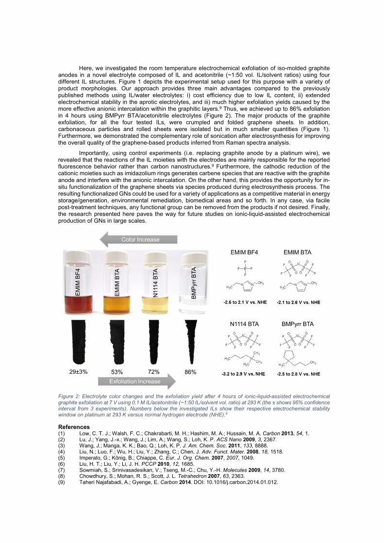
E���,�����������������������������������������3������������ ���7������������������� �� ������ ��������� ����������� +<�������������� .D'B=$� ���*� +<2������ ������0������ ������������ +<����������*�C�����'�������� ���3����������������� ���� ������������,������������������������ �����������*� 6��� ��������� �������� ���� ���� ��������� �������� ��� ��� ������������ ������ ������� ����� +<2,���� ���������B� �0� ����� �������� ��� ��� ��,� +<� ������ ��0� 3�������������������� ������������������������������������0������������3��������������������� ���������������������������������,�����������������������*F�������,��������������A#G�3����������� 8� ������ ����� �%5���� ��92���������� ���������� .C����� !0*� �����H��� ��������� ��� ��� ��������3���������� ���� ���� ��� ����� ����� +<��� ,�� �������� ��� ������ ������ ����*� +� ������������ ������� ��������� ��� ������ ����� ,�� �������� ��� �� ����� ������� -�������� .C����� '0*�C����������,����������������������������������������������������������������������������������-������������������7 �������������������������������������������*�
+����������� ����� ������� 3������� .�**� �������� �������� ���� �� �� ��������,��0�� ,�����������������������������+<��������,������������������������������ ������������������������� ������� ������ ���� ��� �������������*F�C���������� ��� ��������� ����������� �������������������������������4�������������������� ����������������������,����������������������������,�����������������������*�6����������������������������������������������7��������������4�����������������������������������������������������������������*���������������������4���/�������� ��������������������������������������������������������������������2�������� ��������� ���������� ��������� �������� ��� �����*� +���� ����� ���� ����������7�����������-������������������������� �����������������������������������*�C���������� ��������������������� ���,��� ���� ������ ��������� ����7��-���7�����������������������������������/��������������*�
�
�������!������������ �������������� ���� ���� ������������ ������������ "���������� �����#������#������������������� �����������������������������$�%�������&���'�()*��������������+�,&�()*�����������������������! -�.������/������� ,0��������������������� ��� �-� ������ �������1� 2���� 2����� ���� ������������� ()�� ����� ������ ��������������������� ����� ���2����������������������� ����! -�.����������� �����������������������13�� �
�����������.'0� <�,���*��*�I*1�J������C*��*1����:�� ������%*�E*1�E�������%*�9*1�E�������%*�9*�4��2������ ��,"��'*�.!0� <���I*1�K����I*73*1�J����I*1�<����9*1�J����;*1�<����L*�5*�546�1�������!��-��!"#@*�."0� J����I*1�%�����L*�L*1������M*1�<����L*�5*�7��5 ��4�� ��6�����������--��AAAA*�.80� <����/*1�<����C*1�J���E*1�<����K*1�(������*1�����I*�5�����������'���������"���8��'='A*�.=0� +���������*1�L������*1����������*�����7��9����4�� �����#��!&&$��'$8F*�.#0� <����E*��*1�<����K*1�<���I*�E*�:44:��������!��'#A=*�.@0� ;�,������;*1�;����������:���&*1������%*7�*1������K*7E*�'������������!���"��"@A$*�.A0� ���,�������;*1�%������*�;*1�;������I*�<*�;��������������#��<-��!"#"*�.F0� ������/�H��� �����9*1�������*�4��2������$*� 6+B�'$*'$'#2H*��� �*!$'8*$'*$'!*�
Fundamental theoretical limits of graphene tunable and non-reciprocal devices
Michele Tamagnone, Julien Perruisseau-Carrier
Adaptive MicroNano Wave Systems, Ecole Polytechnique Fédérale de Lausanne (EPFL), 1015 Lausanne, Switzerland
In recent years, there has been a surge of interest in graphene-based devices for various terahertz and photonic applications [1-8]. Among other, terahertz tunable metamaterials [1-3], amplitude modulators [4, 5], and isolators have been demonstrated. There is a growing effort to optimize these devices for real applications. However, the absence of guidelines concerning the best possible performances yields to designs having sub-optimal performance or unnecessarily complex structures. We developed a rigorous and general theoretical framework to determine absolute upper bounds on the performances of graphene passive reconfigurable and non-reciprocal devices [8]. Remarkably these limits are related only to graphene conductivity and are independent of the particular geometrical structure of the device. Based on the theory developed, we demonstrate how designs closely approaching these fundamental bounds can be achieved. Our analysis not only provides information on the best possible performances of graphene reconfigurable devices as a function of graphene parameters, but indicates how such optimal performance can be approached by the simplest design. The results are a direct derivation from apply to any graphene reconfigurable or non-reciprocal device. Since the bound apply to any device describable with a scattering matrix, both planar devices and guided ones are subject to it. Additionally, the bound can be easily adapted to other 2D materials. Two examples of bounds that we will present are briefly described here. The first one concerns two states passive reconfigurable devices with a tunable transmission coefficient. These can be either two ports guided device working with confined waves or (meta)surfaces working with free space waves. Let us assume that the tunability is achieved using graphene biased by an electrostatic field. The two states
and which cause the graphene
conductivity to take two distinct values and thanks to the electric field effect. This leads in turn to the two values and of the tunable transmission coefficient. We will show that there is a precise
mathematical bound involving and and depending uniquely on and . Importantly, the bound applies to on-off modulators and switches, tunable passive devices where the design is optimized to maximize one among and and to minimize the other one. The second example concerns graphene non-reciprocal isolators. These devices are based on the tensorial conductivity of graphene under magnetostatic field bias. Non reciprocal two-ports devices are characterized by two different scattering parameters for the signal propagating from port 1 to port 2 and for the one propagating from port 2 to port 1 (namely ). Isolators are devices where one among
and is minimized and the other is maximized. We will show that there is a mathematical bound involving and . Again this bound can be formulated in terms of graphene conductivity only. The complete demonstration of the bounds is inspired by a previous formulation for 3D materials used in circuit theory [9]. In addition, we provide extensive validation of the bound simulating a large number of graphene modulators and isolators having different geometries but identical graphene parameters (and hence the same bound holds for all the devices). No simulated device ever overcame the theoretical limit. Some devices are extremely close to the upper bound and thus they can be considered as optimal. We believe that these bounds represent a very important knowledge advancement on the potential performances of graphene devices and that they provide useful guidelines for maximizing the efficiency of graphene modulators and isolators. References [1] S. H. Lee et al, Nat Mater, 11 (2012) 936-941. [2] A. Fallahi and J. Perruisseau-Carrier, Physical Review B, 86 (2012), 195408. [3] W. Zhu, I. D. Rukhlenko, and M. Premaratne, Applied Physics Letters, 102 (2013) 241914. [4] B. Sensale-Rodriguez et al, Nat Commun, 3(2013) 780. [5] M. Liu et al, Nature, 474(2011) 64-67. [6] M. Tamagnone, J. S. Gomez-Diaz, J. R. Mosig, and J. Perruisseau-Carrier, Applied Physics Letters,
101(2012) 214102-4.

[7] J. Perruisseau-Carrier in LAPC2012, Loughborough (2012). [8] Michele Tamagnone, Arya Fallahi, Juan R. Mosig, and Julien Perruisseau-Carrier, arXiv preprint,
http://arxiv-web3.library.cornell.edu/abs/1308.3068 [9] T. Schaug-pettersen and A. Tonning, Circuit Theory, IRE Transactions on, 6(1959) 150-158.

Tunable Dichroism in One-dimensional Graphene Superlattices
Liang Zheng Tan1, Cheol-Hwan Park
2, Sangkook Choi
1, Steven G. Louie
1
1Department of Physics, University of California, Berkeley, California 94720 and
Materials Sciences Division, Lawrence Berkeley National Laboratory, Berkeley, California 94720, USA
2Department of Physics and Astronomy and Center of Theoretical Physics, Seoul National University,
Seoul 151-747, Korea
Abstract One-dimensional graphene superlattices are periodic potentials on graphene spatially modulated along one direction and constant in the perpendicular direction. These systems can be constructed by the positioning of adatoms on graphene [1], applying local top-gate voltages [2-3], or by placing graphene on a substrate with nanometer scale periodicity [4-6]. The Dirac fermion nature of low energy quasiparticles in graphene is expected to give rise to unusual transport phenomena, such as the proposed supercollimation effect [7-9], in which electron wavepackets are predicted to exhibit dissipationless transport along the modulated direction of the graphene superlattice. In this contribution, we demonstrate theoretically that the optical absorption spectrum provides an alternative route for observing the unusual physics of electrons in graphene superlattices. We show that graphene superlattices exhibit a tunable dichroism effect – different absorbance for different linear polarizations of light (Figure 1). This result is reminiscent of the highly anisotropic transport properties of graphene superlattices at low energies. In addition, we show that the absorption spectrum at optical energy scales contains certain easily identifiable characteristic features. These results enable the observation of graphene superlattice physics via optical means, as well as increasing the range of technological applications of graphene superlattices to the optical domain. We analyze separately periodic graphene superlattices and disordered graphene superlattices. In the former, absorption is increased in the modulated direction and decreased in the constant direction at low frequencies. At higher frequencies, van Hove singularities affect the absorption of light polarized along the constant direction but not the modulated direction, in sharp contrast to the case of the two dimensional electron gas in a periodic potential. For disordered graphene superlattices, we show that the low frequency absorption spectrum behaves in the same way as the periodic case, regardless of the form of the disorder. References [1] P. Järvinen, S.K. Hämäläinen, K. Banerjee, P. Häkkinen, M. Ijäs, A. Harju, and P. Liljeroth, Nano Lett. 13 (2013), 3199. [2] Barbaros Ozyilmaz, Pablo Jarillo-Herrero, Dmitri Efetov, Dmitry A. Abanin, Leonid S. Levitov, and Philip Kim, Phys. Rev. Lett. 99 (2007), 166804-4. [3] J. R. Williams, L. DiCarlo, and C. M. Marcus, Science 317 (2007), 638-641. [4] D. Martoccia, P. R. Willmott, T. Brugger, M. Bjorck, S. Gunther, C. M. Schleputz, A. Cervellino, S. A. Pauli, B. D. Patterson, S. Marchini, J. Wintterlin, W. Moritz, and T. Greber, Phys. Rev. Lett. 101 (2008), 126102-4. [5] M. Yankowitz, J. Xue, D. Cormode, J.D. Sanchez-Yamagishi, K. Watanabe, T. Taniguchi, P. Jarillo-Herrero, P. Jacquod, and B.J. LeRoy, Nat Phys 8 (2012), 382. [6] J.-K. Lee, S. Yamazaki, H. Yun, J. Park, G.P. Kennedy, G.-T. Kim, O. Pietzsch, R. Wiesendanger, S. Lee, S. Hong, U. Dettlaff-Weglikowska, and S. Roth, Nano Lett. 13 (2013), 3494. [7] Cheol-Hwan Park, Li Yang, Young-Woo Son, Marvin L. Cohen, and Steven G. Louie, Phys. Rev. Lett. 101 (2008), 126804-4. [8] L. Brey and H. A. Fertig, Phys. Rev. Lett. 103 (2009), 046809. [9] Cheol-Hwan Park, Young-Woo Son, Li Yang, Marvin L. Cohen, and Steven G. Louie, Nano Letters 8 (2008), 2920-2924.
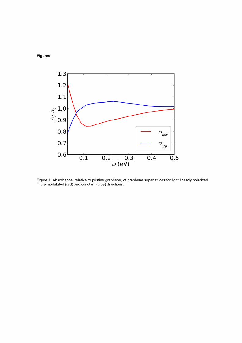
Figures
Figure 1: Absorbance, relative to pristine graphene, of graphene superlattices for light linearly polarized in the modulated (red) and constant (blue) directions.
A new structural model for GO and RGO as revealed by core EELS and DFT
Anna Tararan1,*, Alberto Zobelli
1, Ana Benito
2, Wolfgang Maser
2, Odile Stéphan
1
1Laboratoire de Physique des Solides, Univ. Paris-Sud, CNRS UMR
8502, F-91405, Orsay, France 2Department of Chemical Processes and Nanotechnology, Instituto de Carboquímica ICB-CSIC,
C/Miguel Luesma Castán 4, E-50018 Zaragoza, Spain *[email protected]
Graphite oxide (GO) is a well known material since the middle of the XIX century. In the latest years it
has attracted a renewed fame and interest as a precursor for a cheap large-scale production of
graphene. Indeed, GO conserves the layered structure of graphite with an expanded interlayer distance
that facilitates exfoliation, a subsequent reduction yields a material whose properties are very similar to
those of graphene. Reduced graphene oxide (RGO) properties strongly depend on the local structure
and stoichiometry. However, about 150 years from the first synthesis, many questions remain still open
about GO and RGO chemical homogeneity and the functional groups effectively present.
Previous spectroscopy studies stated that the oxygen content in graphene oxide ranges from 22 to
32%. However, transmission electron microscope images revealed that GO is a very inhomogeneous
material at the nanometer scale. Still, no spatially resolved spectroscopic studies have yet been
reported and only average evaluations are provided in literature. Electron Energy Loss Spectroscopy
(EELS) in a Scanning Transmission Electron Microscope (STEM) could give access to the suitable
scale but GO and RGO are highly sensitive to irradiation.
In this study we overcame this limitation by adopting an experimental set up combining a liquid nitrogen
cooling system at the sample stage, a low accelerated electrons beam (60 keV) and a liquid nitrogen
cooled CCD camera with a low read-out noise of three counts r.m.s. and a negligible dark count noise.
Hyperspectral core EELS images have been then acquired in a low dose mode (order of 105 e
-/nm
2) at
a 10 nm spatial resolution which guaranties a sufficient signal over noise ratio.
Chemical maps for GO and RGO (see figure) show regions within individual flakes with different
oxidation levels confirming the non homogeneity of the material. Whereas oxygen rates averaged over
the whole area are in agreement with literature results, we observe that the oxygen content can locally
rise up to 60%.
Lower oxidized GO regions present fine structure at the carbon K-edge similar to those of amorphous
graphene, while highly oxidized regions present specific core EELS signatures. RGO samples show the
well-known fine structure profile typical of graphite, proving an excellent restoration of the carbon
network. Nevertheless regions characterized by residual oxygen exhibit an additional sharp peak.
These results have been combined with complementary DFT simulations. An analysis of formation and
binding energies for different oxygen functional groups and concentrations and EELS spectra
simulations allowed us to provide a new structural model for GO and RGO compatible with our
experimental findings. Given the extremely high carbon over oxygen ratio, we suggest for the strongly
oxidized regions a structure fully functionalized by hydroxyl groups, while in lower oxidized regions also
the contribution from epoxides is expected.

Fig.1 EELS hyperspectral analysis of a GO and RGO samples: spatially resolved maps of the integrated EELS signal with associated carbon K-shell EELS edges extracted from the marked regions, a chemical map and related histogram showing the occurrence of oxygen content in percentage.

Epitaxial graphene nano flakes on Au(111): Structure, electronic properties and manipulation
Julia Tesch
1, Philipp Leicht
1, Luca Gragnaniello
1, Lukas Zielke
1, Riko Moroni
1, Samuel Bouvron
1, Elena
Voloshina2, Lukas Hammerschmidt
3, Lukas Marsoner Steinkasserer
3, Beate Paulus
3, Yuriy Dedkov
4,
and Mikhail Fonin1
1 Fachbereich Physik, Universität Konstanz, 78457 Konstanz, Germany
2 Institut für Chemie, Humboldt Universität zu Berlin, 12489 Berlin, Germany
3 Institut für Chemie und Biochemie, Freie Universität Berlin 14195 Berlin, Germany
4 SPECS Surface Nano Analysis GmbH, 13355 Berlin, Germany
Abstract Confinement of electrons in graphene quantum dots and nanoribbons presents an exciting field of research, owing to predicted peculiar electronic and magnetic properties [1,2]. Recent attempts with the purpose of measuring the properties of graphene nano dots (GNDs) on Ir(111) have revealed detrimental edge bonding of graphene to the employed iridium substrate [3,4]. We have developed an in-situ fabrication method of graphene nano flakes (GNFs) on the Au(111) noble metal surface. We show that this system is well-suited for STM investigations of the structural and electronic properties of epitaxial GNFs. In the present work, the preparation of GNFs was performed by a two-step process. First well-shaped graphene flakes of different sizes down to several nanometers are prepared on the Ir(111) substrate by temperature programmed growth [5]. Second, a 5 nm thick Au layer is deposited on top of the sample followed by high temperature annealing, yielding embedded and floating GNFs on a high-quality Au(111) surface. We show that flakes can be easily displaced across terraces at room temperature utilizing the STM tip if flakes are initially detached from the Au terraces. The tip-induced displacement of flakes is observed regardless of GNF size by scanning with appropriate tunnelling parameters. Furthermore, eminent quantum interference patterns are observed at the flake edges and compared to DFT calculations of freestanding graphene in order to elucidate edge terminations of the graphene flakes. We observe predominantly single hydrogen terminated, unreconstructed graphene edges, often including long zigzag segments. The electronic properties of the graphene flakes can be accessed via Fourier transform scanning tunnelling spectroscopy (FT-STS). Exploitation of the scattering at defects and edges in the FTs of energy selective local density of states mappings of the graphene honeycomb lattice allows the determination of electronic properties, such as the dispersion relation. For GNFs on Au(111) we measured the expected linear electronic dispersion relation close to the Dirac point which is shifted towards the unoccupied states. References [1] K. Nakada, M. et al., Phys. Rev. B 54 (1996) 17954 [2] O. V. Yazyev, Rep. Prog. Phys. 73 (2010) 056501 [3] D. Subramaniam et al., Phys. Rev. Lett. 108 (2012) 046801 [4] S. J. Altenburg et al., Phys. Rev. Lett. 108 (2012) 206805 [5] J. Coraux et al., New J. Phys. 11 (2009) 023006
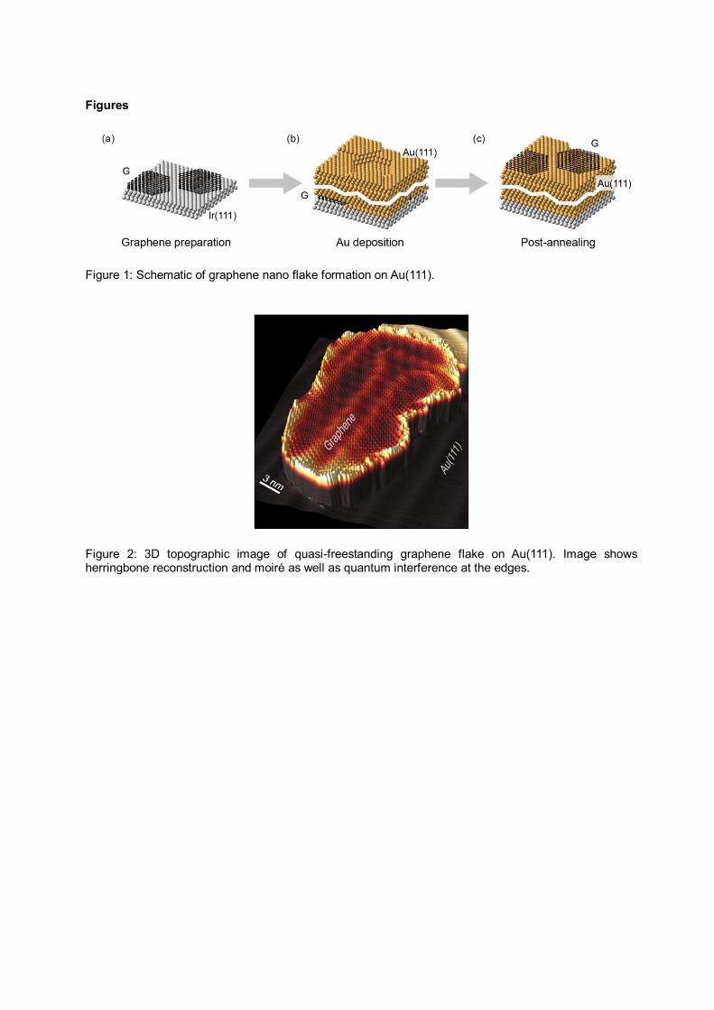
Figures
Figure 1: Schematic of graphene nano flake formation on Au(111).
Figure 2: 3D topographic image of quasi-freestanding graphene flake on Au(111). Image shows herringbone reconstruction and moiré as well as quantum interference at the edges.

Graphene antidot lattices and barriers studied with the Dirac equation
Søren J. Brun, Morten R. Thomsen and Thomas G. Pedersen
Department of Physics and Nanotechnology, Aalborg University, Skjernvej 4A, DK-9220 Aalborg Øst [email protected]
Abstract A band gap can be introduced in graphene by periodic nanoperforation, called a graphene antidot lattice (GAL). This effect has been demonstrated both theoretically [1, 2] and experimentally [3, 4]. Several methods have been used to produce GALs experimentally, including e-beam lithography [3], diblock copolymer templates [4], barrier-guided growth [5], nanosphere lithography [6] and nanoimprint lithography [7]. The antidots range in size between a few nanometers and several hundred nanometers, depending on the fabrication method. Experimentally feasible structures are typically much larger than what traditional theoretical methods, such as tight-binding (TB) or density functional theory, can handle. We present novel methods based on the Dirac equation (DE), which enables us to calculate properties of very large structures. In fact, there is no additional computational cost for increasing the size of the unit cell. We use a spatially varying mass term to model GALs, where the mass term is non-zero in the antidot regions and vanishing elsewhere [2]. The mass term effectively makes electrons massive inside the antidots, which makes it unfavorable to enter them. First, we set up a model that enables us to calculate electronic and optical properties of fully periodic GALs. We compare the results of our models with TB and show excellent agreement in the case of antidots with armchair edges. Figure 1 shows a comparison of bands gap calculated using TB and our Dirac model. Next, we look at electronic transport in graphene antidot barriers (GABs). A GAB can be made by introducing a 1D GAL strip in an otherwise pristine sheet of graphene. We solve this as a scattering problem, where a plane electron wave is incident on a GAB. Using this method, we can calculate the resulting wave function as well as the conductance spectrum of the barrier. An example of the electron probability density of a barrier is shown for different energies in Figure 2. The conductance is high at an energy of 0.15 eV, which results in a high probability density inside the barrier, whereas a low conductance at 0.30 eV results in a low probability density. References [1] T. G. Pedersen et al., Phys. Rev. Lett., 100 (2008) 136804 [2] J. A. Fürst et al., New J. Phys., 11 (2009) 095020 [3] J. Eroms and D. Weiss, New J. Phys., 11 (2009) 095021 [4] J. Bai et al., Nat. Nanotechnol., 5 (2010) 190 [5] N. S. Safron et al., Adv. Mater., 24 (2012) 1041 [6] M. Wang et al., Sci. Rep., 3 (2013) 1238 [7] X. Liang et al., Nano Lett., 10 (2010) 2454

Figures
Figure 1. Comparison of band gaps calculated using TB and the DE.
Figure 2. Electron probability density of a GAB with 4 hexagonal antidots.
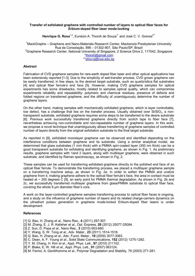
Transfer of exfoliated graphene with controlled number of layers to optical fiber faces for Erbium-doped fiber laser mode-locking
Henrique G. Rosa
1,2, Eunézio A. Thoroh de Souza
1* and José C. V. Gomes
2**
1MackGraphe – Graphene and Nano-Materials Research Center, Mackenzie Presbyterian University
Rua da Consolação, 896 – 01302-907, São Paulo/SP, Brazil 2Graphene Research Center, National University of Singapore, 2 Science Drive 2, 117542, Singapore
*[email protected] **[email protected]
Abstract Fabrication of CVD graphene samples for rare-earth doped fiber laser and other optical applications has been extensively reported [1-3]. Due to the simplicity of wet-transfer process, CVD grown graphene can be easily transferred, in few steps, to the desired target substrate, such as quartz/silica flat substrates [4] and optical fiber ferrule’s end face [5]. However, making CVD graphene samples for optical experiments has some drawbacks, mostly related to samples optical quality, which can compromise experiments reliability and repeatability: polymeric and chemical residues, presence of defects and folded regions on transferred graphene, and the difficulty of unambiguously determine the number of graphene layers. On the other hand, making samples with mechanically exfoliated graphene, which is layer controllable, low defect, has a challenge that lies on the transfer process. Usually obtained over Si/SiO2, a non-transparent substrate, exfoliated graphene requires some steps to be transferred to the desire substrate [6]. Previous work successfully transferred graphene directly from scotch tape to fiber face [7], nevertheless achieving non-controllable and non-repeatable number of graphene layers. In this work, we propose a novel technique that unambiguously allows transferring of graphene samples of controlled number of layers directly from the original exfoliation substrate to the final target substrate. As reported in [8], exfoliated monolayer graphene can be observed and identified depending on the interference conditions between graphene and its substrate. Using a similar analytical model, we determined that glass substrates (1 mm thick) with a PMMA spin-coated layer (300 nm thick) can be a good transparent substrate for exfoliating and identifying graphene, as shown in Fig. 1. As preliminary results, graphene samples with 1and 2 layers, along with multilayer graphene, were obtained in such substrate, and identified by Raman spectroscopy, as shown in Fig. 2. These samples can be used for transferring exfoliated graphene directly to the polished end face of an optical fiber ferrule. To demonstrate the transferring process, we placed a multilayer graphene sample on a transferring machine setup, as shown in Fig. 2a. In order to soften the PMMA and unstick graphene from it, making graphene adhere to the optical fiber ferrule’s face, the area in contact must be heated at ~ 200 degrees C [9], an early point for PMMA thermal degradation. As shown in Fig. 2b and 2c, we successfully transferred multilayer graphene from glass/PMMA substrate to optical fiber face, covering the whole 9 µm diameter fiber’s core. A work on the layer-controlled graphene samples transferring process to optical fiber faces is ongoing, and a study on the influence of graphene number of layers and its related charge-carriers dynamics on the ultrashort pulses generation in graphene mode-locked Erbium-doped fiber lasers is under development. References [1] Q. Bao, H. Zhang et al., Nano Res., 4 (2011) 297-307. [2] M. Zhang, E. J. R. Kelleher et al., Opt. Express, 20 (2012) 25077-25084. [3] Z. Sun, D. Popa et al., Nano Res., 3 (2010) 653-660. [4] Y. Wang, S. W. Tong et al., Adv. Mater., 23 (2011) 1514-1518. [5] Q. Bao, H. Zhang et al., Adv. Funct. Mater., 19 (2009) 3077-3083. [6] C. Dean, A. F. Young et al., Solid State Communications, 152 (2012) 1275-1282. [7] Y. M. Chang, H. Kim et al., Appl. Phys. Lett., 97 (2010) 211102. [8] P. Blake, E. W. Hill et al., Appl. Phys. Lett., 91 (2007) 063124. [9] M. Ferriol, A. Gentilhomme et al., Polymer Degradation and Stability, 79 (2003) 271-281.
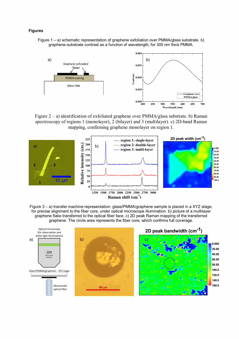
Figures
Figure 1 – a) schematic representation of graphene exfoliation over PMMA/glass substrate. b) graphene-substrate contrast as a function of wavelength, for 300 nm thick PMMA.
400 450 500 550 600 650 7000.040
0.045
0.050
0.055
0.060
Graphene over
PMMA/glass
Co
ntr
ast
Wavelength (nm)
Figure 2 – a) identification of exfoliated graphene over PMMA/glass substrate. b) Raman
spectroscopy of regions 1 (monolayer), 2 (bilayer) and 3 (multilayer). c) 2D-band Raman
mapping, confirming graphene monolayer on region 1.
1250 1500 1750 2000 2250 2500 2750 3000
0
25
50
75
100
125
150
175
200
225
Rela
tive i
nte
nsi
ty (
cts
.)
Raman shift (cm-1)
region 1: single-layer
region 2: double-layer
region 3: multi-layer
2D peak width (cm-1)
0.000
10.00
20.00
30.00
40.00
50.00
60.00
70.00
80.00
90.00
100.0
Figure 3 – a) transfer machine representation: glass/PMMA/graphene sample is placed in a XYZ stage, for precise alignment to the fiber core, under optical microscope illumination. b) picture of a multilayer
graphene flake transferred to the optical fiber face. c) 2D peak Raman mapping of the transferred graphene. The circle area represents the fiber core, which confirms full coverage.
20XMicroscope
objective
Optical microscope
(for observation and
white light Illumination)
Glass/PMMA/graphene – XYZ stage
Monomode
optical fiber
2D peak bandwidth (cm-1)
0.000
20.00
40.00
60.00
80.00
100.0
120.0
140.0
160.0
a) b)
a) b) c)
a) b) c)
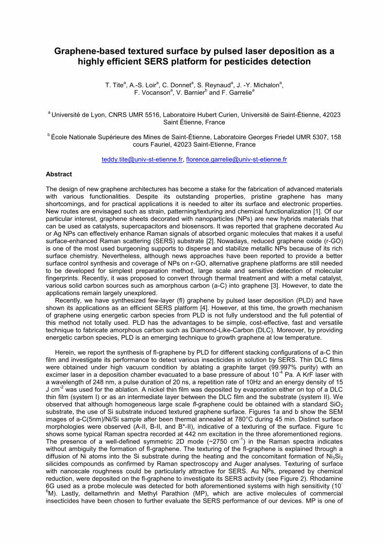
Graphene-based textured surface by pulsed laser deposition as a highly efficient SERS platform for pesticides detection
T. Titea, A.-S. Loir
a, C. Donnet
a, S. Reynaud
a, J. -Y. Michalon
a,
F. Vocansona, V. Barnier
b and F. Garrelie
a
a Université de Lyon, CNRS UMR 5516, Laboratoire Hubert Curien, Université de Saint-Étienne, 42023
Saint Étienne, France
b École Nationale Supérieure des Mines de Saint-Étienne, Laboratoire Georges Friedel UMR 5307, 158
cours Fauriel, 42023 Saint-Etienne, France
[email protected], [email protected]
Abstract The design of new graphene architectures has become a stake for the fabrication of advanced materials with various functionalities. Despite its outstanding properties, pristine graphene has many shortcomings, and for practical applications it is needed to alter its surface and electronic properties. New routes are envisaged such as strain, patterning/texturing and chemical functionalization [1]. Of our particular interest, graphene sheets decorated with nanoparticles (NPs) are new hybrids materials that can be used as catalysts, supercapacitors and biosensors.
It was reported that graphene decorated Au
or Ag NPs can effectively enhance Raman signals of absorbed organic molecules that makes it a useful surface-enhanced Raman scattering (SERS) substrate [2].
Nowadays, reduced graphene oxide (r-GO)
is one of the most used burgeoning supports to disperse and stabilize metallic NPs because of its rich surface chemistry. Nevertheless, although news approaches have been reported to provide a better surface control synthesis and coverage of NPs on r-GO, alternative graphene platforms are still needed to be developed for simplest preparation method, large scale and sensitive detection of molecular fingerprints. Recently, it was proposed to convert through thermal treatment and with a metal catalyst, various solid carbon sources such as amorphous carbon (a-C) into graphene [3]. However, to date the applications remain largely unexplored.
Recently, we have synthesized few-layer (fl) graphene by pulsed laser deposition (PLD) and have shown its applications as an efficient SERS platform [4]. However, at this time, the growth mechanism of graphene using energetic carbon species from PLD is not fully understood and the full potential of this method not totally used. PLD has the advantages to be simple, cost-effective, fast and versatile technique to fabricate amorphous carbon such as Diamond-Like-Carbon (DLC). Moreover, by providing energetic carbon species, PLD is an emerging technique to growth graphene at low temperature.
Herein, we report the synthesis of fl-graphene by PLD for different stacking configurations of a-C thin film and investigate its performance to detect various insecticides in solution by SERS. Thin DLC films were obtained under high vacuum condition by ablating a graphite target (99.997% purity) with an excimer laser in a deposition chamber evacuated to a base pressure of about 10
-4 Pa. A KrF laser with
a wavelength of 248 nm, a pulse duration of 20 ns, a repetition rate of 10Hz and an energy density of 15 J cm
-2 was used for the ablation. A nickel thin film was deposited by evaporation either on top of a DLC
thin film (system I) or as an intermediate layer between the DLC film and the substrate (system II). We observed that although homogeneous large scale fl-graphene could be obtained with a standard SiO2 substrate, the use of Si substrate induced textured graphene surface. Figures 1a and b show the SEM images of a-C(5nm)/Ni/Si sample after been thermal annealed at 780°C during 45 min. Distinct surface morphologies were observed (A-II, B-II, and B*-II), indicative of a texturing of the surface. Figure 1c shows some typical Raman spectra recorded at 442 nm excitation in the three aforementioned regions. The presence of a well-defined symmetric 2D mode (~2750 cm
-1) in the Raman spectra indicates
without ambiguity the formation of fl-graphene. The texturing of the fl-graphene is explained through a diffusion of Ni atoms into the Si substrate during the heating and the concomitant formation of Ni3Si2 silicides compounds as confirmed by Raman spectroscopy and Auger analyses. Texturing of surface with nanoscale roughness could be particularly attractive for SERS. Au NPs, prepared by chemical reduction, were deposited on the fl-graphene to investigate its SERS activity (see Figure 2). Rhodamine 6G used as a probe molecule was detected for both aforementioned systems with high sensitivity (10
-
6M). Lastly, deltamethrin and Methyl Parathion (MP), which are active molecules of commercial
insecticides have been chosen to further evaluate the SERS performance of our devices. MP is one of

the most toxic organophosphate pesticides. Recently, Yazdi et al. have detected MP with high sensitivity (5 ppm) using an original method [5]. Figures 3a and b show typical Raman spectra of MP at different concentrations (10
-5M and 10
-4M) obtained on the fl-graphene. Distinct Raman features at
around 859, 1110, and 1344 cm-1
that are characteristic peaks of MP are clearly observed for a MP
concentration as low as 10-5
M (3 ppm). The method developed is simple, fast and cost effective.
References [1] V. Georgakilas et al., Chem. Rev., 112(2012), 6156. [2] W. Xu et al., Small 9, 8(2013), 1206. [3] C. M. Orofeo et al., Nano Res., 4, 6(2011), 531. [4] T. Tite et al., Appl. Phys. Lett., 1045(2014), 041912. [5] S. H. Yazdi, I. M. White, Analyst, 138(2013), 100.
Figures
Figure 1. SEM images of a-C(5nm)/Ni/Si after thermal processing at a) 500× and b) 6000× magnifications. (c) typical Raman spectra at 442 nm laser excitation recorded in the regions A-I, B-I and C-I.
Figure 2. a) TEM image of Au nanoparticles; b) typical SEM image of Au NPs decorated few-layer graphene.
Figure 3. Raman spectra at 633 nm of aqueous methyl parathion deposited on a) AuNPs/fl-G (system I, Ni/a-C(5nm)/Si) and b) (system II, a-C(5nm)/Ni/Si) at concentrations 10
-5M and 10
-4M. The arrows indicate the peaks signature of methyl
parathion.

Study on Non-covalently Stabilzed Graphene in chemical PVA-MA based Hydrogel
Yosra Toumia, Silvia Orlanducci and Gaio Paradossi
Currently, graphene has been the most attractive nanomaterial in the scientific community and has lead
to an explosion of creativity and productivity in different fields due to its 2D planar structure and its
unique fascinating chemical and physical properties [1]
.
In the recent years, graphene has become a prevalent topic in the materials community, crossing
numerous studies on soft materials aiming at biomedical applications such as sustained drug delivery.
Thus, graphene and its derivatives such as graphene oxide (GO) and reduced graphene oxide (rGO)
inspired the investigators to try to incorporate them in hydrogels, taking advantage of the flexible and
ultrathin planar structure of graphene sheets in constructing a 3D network of hydrogels [2]
. Most
researches reported the use of graphene derivatives in hydrogels (as GO and rGO) because of the
relatively high concentrated dispersions achieved by modifying the graphene surface structure through
the oxidation process (up to 7 mg/ml) [3]
. However, the use of pristine graphene is still limited. Herein, to
the extent that we do not damage the structure and preserve the electric properties that does the
pristine graphene have, we have directly exfoliated graphite to graphene in water-surfactant solution.
-
2,4,6-tris(1-phenylethyl)phenyl ether methacrylate used as surfactant, we expect to preserve the
graphene structure. Optimization of the conditions to obtain stable dispersions with a significant
graphene content elicited the Raman characterization of the samples in order to gain information
regarding the exfoliation quality and the presence of graphene monolayer as well as flakes formed by
few layers sheets with limited defects. The surfactant functionalized graphene was then crosslinked via
a free radical photo-polymerization to methacryloyl- modified polyvinyl alcohol (PVA-MA), a widely used
polymer because of its good mechanical properties and biocompatibility [4]
, to form an hybrid hydrogel,
i.e. graphene/PVA-MA/H2O. The incorporation of graphene sheets in the hydrogel was confirmed by
Raman spectroscopy. The hybrid hydrogel was characterized using rheology, differential scanning
with respect to the native hydrogel, despite the low amount (0.1mg/ml) of graphene. In another
experiment, oligomers of poly(N-isopropylacrylamide), pNiPAAm, a well known thermosensitive
polymer, were also incorporated. In this way the graphene based hydrogel exhibits an additional
property such as thermoresponsivity characterized by a volume phase transition at temperatures close
to 37 °C.
Hydrogels based on multifunctionality and with interesting mechanical properties are a promoting
material for wide applications in the design of drug carriers systems, tissue engineering and
biosensoring.
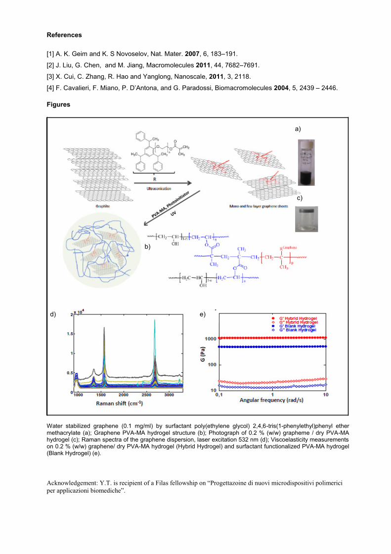
References
[1] A. K. Geim and K. S Novoselov, Nat. Mater. 2007, 6, 183 191.
[2] J. Liu, G. Chen, and M. Jiang, Macromolecules 2011, 44, 7682 7691.
[3] X. Cui, C. Zhang, R. Hao and Yanglong, Nanoscale, 2011, 3, 2118.
[4] F. Cavalieri, F. Miano, P. . Paradossi, Biomacromolecules 2004, 5, 2439 2446.
Figures
Water stabilized graphene (0.1 mg/ml) by surfactant poly(ethylene glycol) 2,4,6-tris(1-phenylethyl)phenyl ether methacrylate (a); Graphene PVA-MA hydrogel structure (b); Photograph of 0.2 % (w/w) grapheme / dry PVA-MA hydrogel (c); Raman spectra of the graphene dispersion, laser excitation 532 nm (d); Viscoelasticity measurements on 0.2 % (w/w) graphene/ dry PVA-MA hydrogel (Hybrid Hydrogel) and surfactant functionalized PVA-MA hydrogel (Blank Hydrogel) (e).
a)
b)
c)
d) e)
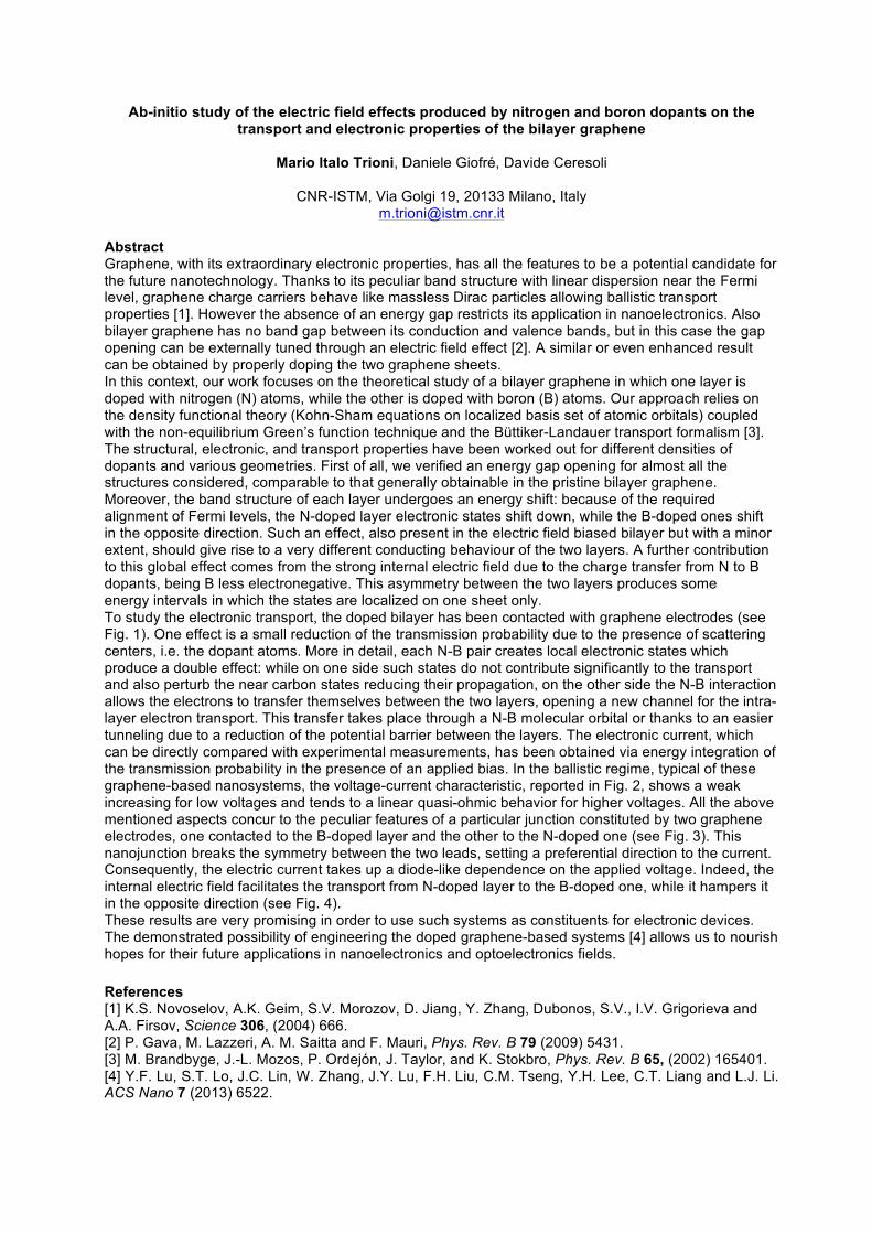
Ab-initio study of the electric field effects produced by nitrogen and boron dopants on the transport and electronic properties of the bilayer graphene
Mario Italo Trioni, Daniele Giofré, Davide Ceresoli
CNR-ISTM, Via Golgi 19, 20133 Milano, [email protected]
Abstract Graphene, with its extraordinary electronic properties, has all the features to be a potential candidate for the future nanotechnology. Thanks to its peculiar band structure with linear dispersion near the Fermi level, graphene charge carriers behave like massless Dirac particles allowing ballistic transport properties [1]. However the absence of an energy gap restricts its application in nanoelectronics. Also bilayer graphene has no band gap between its conduction and valence bands, but in this case the gap opening can be externally tuned through an electric field effect [2]. A similar or even enhanced result can be obtained by properly doping the two graphene sheets.In this context, our work focuses on the theoretical study of a bilayer graphene in which one layer is doped with nitrogen (N) atoms, while the other is doped with boron (B) atoms. Our approach relies on the density functional theory (Kohn-Sham equations on localized basis set of atomic orbitals) coupled with the non-equilibrium Green’s function technique and the Büttiker-Landauer transport formalism [3].The structural, electronic, and transport properties have been worked out for different densities of dopants and various geometries. First of all, we verified an energy gap opening for almost all the structures considered, comparable to that generally obtainable in the pristine bilayer graphene. Moreover, the band structure of each layer undergoes an energy shift: because of the required alignment of Fermi levels, the N-doped layer electronic states shift down, while the B-doped ones shift in the opposite direction. Such an effect, also present in the electric field biased bilayer but with a minor extent, should give rise to a very different conducting behaviour of the two layers. A further contribution to this global effect comes from the strong internal electric field due to the charge transfer from N to B dopants, being B less electronegative. This asymmetry between the two layers produces some energy intervals in which the states are localized on one sheet only.To study the electronic transport, the doped bilayer has been contacted with graphene electrodes (see Fig. 1). One effect is a small reduction of the transmission probability due to the presence of scattering centers, i.e. the dopant atoms. More in detail, each N-B pair creates local electronic states which produce a double effect: while on one side such states do not contribute significantly to the transport and also perturb the near carbon states reducing their propagation, on the other side the N-B interaction allows the electrons to transfer themselves between the two layers, opening a new channel for the intra-layer electron transport. This transfer takes place through a N-B molecular orbital or thanks to an easier tunneling due to a reduction of the potential barrier between the layers. The electronic current, which can be directly compared with experimental measurements, has been obtained via energy integration of the transmission probability in the presence of an applied bias. In the ballistic regime, typical of these graphene-based nanosystems, the voltage-current characteristic, reported in Fig. 2, shows a weak increasing for low voltages and tends to a linear quasi-ohmic behavior for higher voltages. All the above mentioned aspects concur to the peculiar features of a particular junction constituted by two graphene electrodes, one contacted to the B-doped layer and the other to the N-doped one (see Fig. 3). This nanojunction breaks the symmetry between the two leads, setting a preferential direction to the current. Consequently, the electric current takes up a diode-like dependence on the applied voltage. Indeed, the internal electric field facilitates the transport from N-doped layer to the B-doped one, while it hampers it in the opposite direction (see Fig. 4).These results are very promising in order to use such systems as constituents for electronic devices. The demonstrated possibility of engineering the doped graphene-based systems [4] allows us to nourish hopes for their future applications in nanoelectronics and optoelectronics fields.
References[1] K.S. Novoselov, A.K. Geim, S.V. Morozov, D. Jiang, Y. Zhang, Dubonos, S.V., I.V. Grigorieva andA.A. Firsov, Science 306, (2004) 666.[2] P. Gava, M. Lazzeri, A. M. Saitta and F. Mauri, Phys. Rev. B 79 (2009) 5431.[3] M. Brandbyge, J.-L. Mozos, P. Ordejón, J. Taylor, and K. Stokbro, Phys. Rev. B 65, (2002) 165401.[4] Y.F. Lu, S.T. Lo, J.C. Lin, W. Zhang, J.Y. Lu, F.H. Liu, C.M. Tseng, Y.H. Lee, C.T. Liang and L.J. Li. ACS Nano 7 (2013) 6522.

Figures
!"#$%&'()$*+( ,*-.$%&'()$*+(/)0$$",",!"
#
$"
$#
$! "
%&" !&# !&" " &# " &" " &# !&" !&# %&"
'$(µ)*+,
-'./$(0,
-1
$"
$!
$%
$3
��5% &" 5! &# 5! &" 5"&# $"&" $"&# $! &" $! &# $% &"
6(7,
789:;<57=$(90,
-15-2
-2
!"#$%&'()$*+( ,*-.$%&'()$*+(/)0$$",", !"#
!"$
$"#
$"$
$"#
!"$
!"#
!"# !"$ $"# $"$ $"# !"$ !"#
%&'µ()*+
,%-.&'/+
,0 ,1
,1
$"$
$
$"3
$"4
$"5
!"$
62"$ 6! "# 6! "$ 6$"# $"$ $"# ! "$ ! "# 2"$
7'8+
89:;<=68>&':/+
,06,1
,1
Figure 1 Geometry of the BN doped junction. The upper layer
contains the nitrogen atom while the lower layer contains the
boron one.
Figura 2 I-V characteristic of the system reported in
Fig. 1. The inset reports the transmission probability
at ∆V=-1.4 V.
Figure 3 Geometry of the n-p BN doped nanojunction. The
upper layer contains the nitrogen atom while the lower layer
contains the boron one.
Figura 4 I-V characteristic of the system reported in
Fig. 3. The inset reports the transmission probability
at ∆V=-1.4 V.

Improved the conductivity of the carbon nanotubes by iodine doping: a DFT study
Damien Tristant, Iann Gerber, Pascal Puech
Département de Génie Physique, INSA
Laboratoire de Physique et Chimie de Nano-Objets LPCNO
Equipe Modélisation Physique et Chimique
Université de Toulouse
135 avenue de Rangueil
31077 Toulouse Cedex
France
Abstract
Since its discovery, significant researches have tried to understand and use the electronic
transport properties of carbon nanotubes (CNTs) to create more efficient new components. One way
to improve significantly the conductivity of CNT bundles is to put them in interaction with iodine vapor.
[1,2] However little is known about the origin of such an improvement at the atomic scale. The major
target of this theoretical/experimental study is to analyze the interaction between iodine complexes
and carbon based nanostructures and to rationalize it to predict induced changes in the electronic
structures by chemical doping by halogens species. The final goal will be to compare electronic
transmission of two crossed carbon nanotubes by junction molecules both theoretically and
experimentally.
At the very beginning of this work, we have focused our computational effort on the
comparison of the adsorption modes and the induced modifications of the electronic structures (Fermi
level shifts and hybridization of bands) by atoms and molecules belonging to the family of halogens,
and on a graphene layer, which can be considered as a reasonable model of large CNT (Fig. 1).
Our first results are in good agreement with previous studies [3-4]. They confirm that the molecule
prefers to adsorb on a specific site, as soon as the concentration remains low, < 2%, with an
adsorption energy of around -0.4 eV, when van der Waals forces are included. More interestingly the
molecular state is more stable than the dissociated one. However experimentally charged complexes
like or are detected [2]. By looking at the interaction of stable molecule with highly reactive sites
like monovacancy, we propose a mechanism of formation of these ions compatible with the hole-
doping observation of the carbon nanostructures. Finally by varying the concentration of absorbates
one should be able to tune the density of states and doing so the conductivity of CNTs.
References
[1] Y. Zhao, J. Wei, R. Vajtai, P. M. Ajayan and E. V. Barrera, Sci. Rep. 1, p. 83 (2011).
[2] L. Grigorian et al, Phys. Rev. Lett. 80, p. 5560 (1998).
[3] Xiaofeng Luo, Chao Fang, Xin Li, Wensheng Lai, Tongxiang Liang, J. Nucl. Mat. 441, p. 113
(2013).
[4] A. N. Rudenko, F. J. Keil, M. I. Katsnelson, A. I. Lichtenstein, Phys. Rev. B 82, p. 035427 (2010).

Figures
Figure 1: The coverage of admolecules. The sketch diagram shows four admolecules on CNTs with a
large radius curvature, with 4x4 primitive cells.

Perforation of the Graphene Layers via High Temperature Acidic Treatment of Graphite Oxide
Tur V.A., Fedorovskaya E.O., Bulusheva L.G., Okotrub A.V.
Nikolaev Institute of Inorganic Chemistry SB RAS, Novosibirsk, Russia [email protected]
Currently graphene-based materials are attracting an increasing attention in various applications,
e.g. as electrodes in supercapacitors, due to its high electrical conductivity and chemical stability. Of particular interest is the structure with a large number of vacancy defects in the carbon layers, because these defects can help electrolyte ions to diffuse between the layers which can lead to improving of electrochemical performance of material. At the same time the carbon atoms on the edges of defects accumulate charge more efficiently than the atoms on the basal plane. These factors can lead to a substantial increasing of electrode specific capacity. Another factor that can be very important is the functionalization of the carbon layers. The presence of functional groups can improve the interaction of electrode surface with electrolyte and, in addition, be involved in redox processes which in turn lead to an additional pseudocapacity appearance.
In this work the method of obtaining of material which has a large number of vacancy defects in graphene layers (called perforated graphite PG) and can be exfoliated with the formation of perforated graphene was proposed. This method involves heat treatment of graphite oxide in concentrated mineral acids, such as sulfuric, phosphoric acid or the mixture of these acids [1]. The effect of treatment time and temperature, as well as the acid choice on the structure, functional composition and electrochemical properties of the final product was also investigated [2]. It was found that the
parameters and can be controlled by adjusting the relevant temperatures and processing times, as well as the proportion of acids in a mixture. Study of the electrochemical properties of the carbon material showed that the capacity of an electrode made of the perforated graphite may reach values of 140 F/g. Such a high capacity can be explained by the presence of vacancy defects in the structure of perforated graphite, as well as the contribution of redox processes. Based on the obtained data the mechanism of the vacancy defects formation was proposed with using the methods of quantum chemistry and computer modeling. [1] A.V. Okotrub, N.F. Yudanov, V.A. Tur et al., Physica Status Solidi B., 12 (2012)., pp. 2620-2624. [2] V.A. Tur, A.V. Okotrub, M.M. Shmakov et al., Physica Status Solidi B., 12 (2013)., pp. 27470-2752.
Fig 1. High resolution (2 nm) TEM image of the perforated graphite sample.
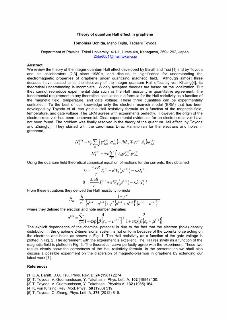
Theory of quantum Hall effect in graphene
Tomohisa Uchida, Maho Fujita, Tadashi Toyoda
Department of Physics, Tokai University, 4-1-1, Hiratsuka, Kanagawa, 259-1292, Japan
Abstract We review the theory of the integer quantum Hall effect developed by Baraff and Tsui [1] and by Toyoda and his collaborators [2,3] since 1980 s, and discuss its significance for understanding the electromagnetic properties of graphene under quantizing magnetic field. Although almost three decades have passed since the discovery of the integer quantum Hall effect by von Klitzing[4], its theoretical understanding is incomplete. Widely accepted theories are based on the localization. But they cannot reproduce experimental data such as the Hall resistivity in quantitative agreement. The fundamental requirement to any theoretical calculation is a formula for the Hall resistivity as a function of the magnetic field, temperature, and gate voltage. These three quantities can be experimentally controlled. To the best of our knowledge only the electron reservoir model (ERM) that has been developed by Toyoda et al. can yield a Hall resistivity formula as a function of the magnetic field, temperature, and gate voltage. The ERM agrees with experiments perfectly. However, the origin of the electron reservoir has been controversial. Clear experimental evidences for an electron reservoir have not been found. The problem was finally resolved in the theory of the quantum Hall effect by Toyoda and Zhang[5]. They started with the zero-mass Dirac Hamiltonian for the electrons and holes in graphene,
K
Kjj
j
KF AecivH )(1)()(
0
K
KKAeH )()(
0
)(
1
Using the quantum field theoretical canonical equation of motions for the currents, they obtained
)(
1
)(
1
2)(
20 IVeIc
eB
)(
2
1)(
2
2)(
10 IVeIc
eB
From these equations they derived the Hall resistivity formula
1)()(2)()(2)()(
2
2
1
nnnnnne
hRH
where they defined the electron and hole number densities
1)(
0
)(
)(
exp1
2
exp1
4
N N
n
The explicit dependence of the chemical potential is due to the fact that the electron (hole) density distribution in the graphene 2-dimensional system is not uniform because of the Lorentz force acting on the electrons and holes as shown in Fig. 1. The Hall resistivity as a function of the gate voltage is plotted in Fig. 2. The agreement with the experiment is excellent. The Hall resistivity as a function of the magnetic field is plotted in Fig. 3. The theoretical curve perfectly agree with the experiment. These two results clearly show the correctness of the Hall resistivity formula. In the presentation we shall also discuss a possible experiment on the dispersion of magneto-plasmon in graphene by extending our latest work [7]. References [1] G.A. Baraff, D.C. Tsui, Phys. Rev. B, 24 (1981) 2274. [2] T. Toyoda, V. Gudmundsson, Y. Takahashi, Phys. Lett. A, 102 (1984) 130. [3] T. Toyoda, V. Gudmundsson, Y. Takahashi, Physica A, 132 (1985) 164 [4] K. von Klitzing, Rev. Mod. Phys., 58 (1986) 519. [5] T. Toyoda, C. Zhang, Phys. Lett. A, 376 (2012) 616.
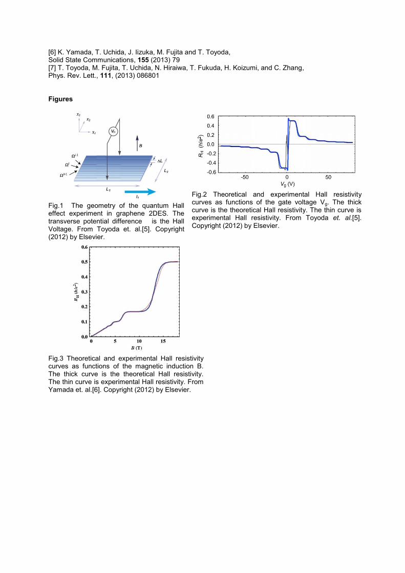
[6] K. Yamada, T. Uchida, J. Iizuka, M. Fujita and T. Toyoda, Solid State Communications, 155 (2013) 79 [7] T. Toyoda, M. Fujita, T. Uchida, N. Hiraiwa, T. Fukuda, H. Koizumi, and C. Zhang, Phys. Rev. Lett., 111, (2013) 086801 Figures
Fig.1 The geometry of the quantum Hall effect experiment in graphene 2DES. The transverse potential difference is the Hall Voltage. From Toyoda et. al.[5]. Copyright (2012) by Elsevier.
Fig.2 Theoretical and experimental Hall resistivity curves as functions of the gate voltage Vg. The thick curve is the theoretical Hall resistivity. The thin curve is experimental Hall resistivity. From Toyoda et. al.[5]. Copyright (2012) by Elsevier.
Fig.3 Theoretical and experimental Hall resistivity curves as functions of the magnetic induction B. The thick curve is the theoretical Hall resistivity. The thin curve is experimental Hall resistivity. From Yamada et. al.[6]. Copyright (2012) by Elsevier.
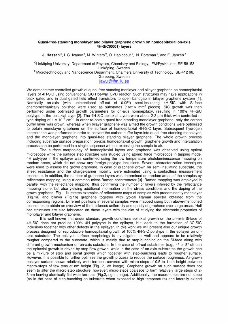
Quasi-free-standing monolayer and bilayer graphene growth on homoepitaxial on-axis 4H-SiC(0001) layers
J. Hassan a, I. G. Ivanov
a, M. Winters
b, O. Habibpour
b, N. Rorsman
b, and E. Janzén
a
a)Linköping University, Department of Physics, Chemistry and Biology, IFM/Fysikhuset, SE-58153
Linköping, Sweden b)
Microtechnology and Nanoscience Department, Chalmers University of Technology, SE-412 96, Goteborg, Sweden
We demonstrate controlled growth of quasi-free standing monlayer and bilayer graphene on homoepitaxial layers of 4H-SiC using conventional SiC Hot-wall CVD reactor. Such structures may have applications in back gated and in dual gated field effect transistors to open bandgap in bilayer graphene system [1]. Nominally on-axis (with unintentional off-cut of 0.05º) semi-insulating 4H-SiC with Si-face chemomechanically polished were used as substrates (16x16 mm
2 pieces). SiC growth was then
performed under optimized growth parameters for on-axis homoepitaxy, resulting in 100% 4H-SiC polytype in the epitaxial layer [2]. The 4H-SiC epitaxial layers were about 2-3 µm thick with controlled n-type doping of 1 x 10
16 cm
-3. In order to obtain quasi-free-standing monolayer graphene, only the carbon
buffer layer was grown, whereas when bilayer graphene was aimed the growth conditions were optimized to obtain monolayer graphene on the surface of homoepitaxial 4H-SiC layer. Subsequent hydrogen intercalation was performed in order to convert the carbon buffer layer into quasi-free-standing monolayer, and the monolayer graphene into quasi-free standing bilayer graphene. The whole growth process including substrate surface preparation, on-axis homoepitaxial growth, graphene growth and intercalation process can be performed in a single sequence without exposing the sample to air.
The surface morphology of homoepitaxial layers and graphene was observed using optical microscope while the surface step structure was studied using atomic force microscope in tapping mode. 4H polytype in the epilayer was confirmed using the low temperature photoluminescence mapping on random areas, which did not show any foreign polytype inclusions. Several characterization techniques were used to assess the grown graphene. In case of graphene grown on semi-insulating substrate, the sheet resistance and the charge-carrier mobility were estimated using a contactless measurement technique. In addition, the number of graphene layers was determined on random areas of the samples by reflectance mapping using a common micro-Raman spectrometer [3]. Raman mapping was employed in parallel with the reflectance mapping, thus confirming the number of layers inferred by the reflectance mapping alone, but also yielding additional information on the stress conditions and the doping of the grown graphene. Fig. 1 illustrates examples of reflectance maps of samples with predominantly monolayer (Fig.1a) and bilayer (Fig.1b) graphene together with typical Raman spectra obtained from the corresponding regions. Different positions in several samples were mapped using both above-mentioned techniques to obtain an overview of the thickness uniformity and quality of graphene over large areas. Hall bar structures are also fabricated on these layers with the aim of studying the electronic properties of monolayer and bilayer graphene.
It is well known that under standard growth conditions epitaxial growth on the on-axis Si-face of 4H-SiC does not produce 100% 4H polytype in the epilayer, but leads to the formation of 3C-SiC inclusions together with other defects in the epilayer. In this work we will present also our unique growth process designed for reproducible homoepitaxial growth of 100% 4H-SiC polytype in the epilayer on on-axis substrate. The epilayer surface morphology is investigated as well and appears to be relatively rougher compared to the substrate, which is mainly due to step-bunching on the Si-face along with
different growth mechanism on on-axis substrate. In the case of off-cut substrates (e.g., 4° or 8° off-cut) the epitaxial growth is driven by step-flow growth, while in the case of on-axis substrates the growth can be a mixture of step and spiral growth which together with step-bunching leads to rougher surface. However, it is possible to further optimize the growth process to reduce the surface roughness. As-grown epilayer surface shows relatively wide terraces covered with micro-steps of 0.5 to 1 nm height between macro-steps of few tens of nm height (Fig. 2, left image). Graphene growth on such surface does not seem to alter the macro-step structure, however; micro-steps coalesce to form relatively large steps of 2-3 nm leaving atomically flat wide terraces (Fig.2, right image). Additionally, the macro-steps are not steep (as in the case of step-bunching on substrate when exposed to high temperature) and laterally extend
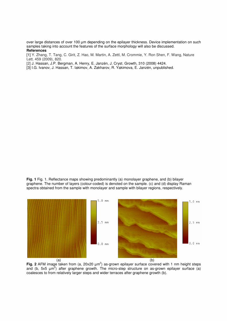
over large distances of over 100samples taking into account the features of the suReferences [1] Y. Zhang, T. Tang, C. Girit, Z. Hao, M. Martin, A. Lett. 459 (2009), 820. [2] J. Hassan, J.P. Bergman, A. Henry, E. Janz[3] I.G. Ivanov, J. Hassan, T. Iakimov, A. Zakharov, R.
Fig. 1 Fig. 1. Reflectance maps showing predominantly (a) graphene. The number of layersspectra obtained from the sample with
(a) Fig. 2 AFM image taken from (aand (b, 5x5 µm
2) after graphene growth. The micro
coalesces to from relatively large
µm depending on the epilayer thickness. Device implementation on such samples taking into account the features of the surface morphology will also be discussed.
Y. Zhang, T. Tang, C. Girit, Z. Hao, M. Martin, A. Zettl, M. Crommie, Y. Ron Shen, F. Wang, Nature
J. Hassan, J.P. Bergman, A. Henry, E. Janzén, J. Cryst. Growth, 310 (2008) 4424.I.G. Ivanov, J. Hassan, T. Iakimov, A. Zakharov, R. Yakimova, E. Janzén, unpublished.
Fig. 1. Reflectance maps showing predominantly (a) monolayer graphene, and (b) bilayer (colour-coded) is denoted on the sample. (c) and (d) display Raman
sample with monolayer and sample with bilayer regions, respectively.
(b) (a, 20x20 µm
2) as-grown epilayer surface covered with 1
) after graphene growth. The micro-step structure on as-grown epilayer surface (a) coalesces to from relatively larger steps and wider terraces after graphene growth (b)
Device implementation on such rface morphology will also be discussed.
Zettl, M. Crommie, Y. Ron Shen, F. Wang, Nature
(2008) 4424. Yakimova, E. Janzén, unpublished.
monolayer graphene, and (b) bilayer is denoted on the sample. (c) and (d) display Raman
bilayer regions, respectively.
grown epilayer surface covered with 1 nm height steps grown epilayer surface (a)
er graphene growth (b).
HYDROTHERMAL EXFOLIATION OF GRAPHITE TO PRODUCE FEW-LAYER GRAPHENE
C. Vacacela-Gómez,
1,2 G. Tubón,
1,2 D. Coello,
1,2 L. Caputi,
1 A. Tavolaro
2
1 Surface Nanoscience Group, Departament of Physics, University of Calabria, Via P. Bucci 31/c, I-
87036 Rende (CS), Italy 2 Research Institute on Membrane Technology (ITM-CNR), National Research Council of Italy c/o
University of Calabria, Via P. Bucci 17/c, I-87036 Rende (CS), Italy
Abstract (POSTER ONLY)
This poster describes an easy exfoliation of graphite in surfactant-water solution1. Here, we report that
pristine graphite heat-treated (pre-treatment) in an autoclave for 15 hours at 180 ºC2 with a surfactant-
water solution improves the process of sonication. The cationic surfactant hexadecyltrimethylammonium
Bromide (CTAB)3,4
, used in this work can be exploited both as dispersant and stabilizer, for pre-
treatment and direct exfoliation of graphite, without the continuous addition of surfactant5, without a
polymer stabilizer2 and without extensive sonication periods
6. Scanning Electron Microscope shows: (i)
the distance between the layers increases in the pre-treatment of graphite without significant damage to
the crystal structure, and (ii) thin and semitransparent films about 3 to 10 µm after the sonication
process were observed. The absorption spectrum of graphene in the surfactant-water solution shows a
s that graphene absorption
spectrum is flat and featureless.7,8
Raman spectroscopy allows to observe a D peak, can be attributed
to the surfactant/graphene interaction, and not to a disorder in the structure, also a 2D peak is observed
comparable to previous reports <5 layers1. The graphene suspended was stable for several months
without a substantial sedimentation and it
onto surface its electronic properties, which can be used in a wide
range of applications. This work opens the possibility of improving the heat-treated of graphite with other
surfactants.
References
[1] M. Lotya, Y. Hernandez, P. J. King, R. J. Smith, V. Nicolosi, L. S. Karlsson, F. M. Blighe, S. De, Z. Wang, I. T. McGovern, G. S. Duesberg and J. N. Coleman, J. Am. Chem. Soc., 2009, 131, 3611-3620
[2] E. Ou, Y. Xie, C. Peng, Y. Song, H. Peng, Y. Xiong, and W. Xu, RSC Advances, 2013, 3(24), 9490-9499.
[3] S. Vadukumpully, J. Paul and S. Valiyaveettil, Carbon, 2009, 47(14), 3288-3294. [4] R. Rastogi, R. Kaushal, S. K. Tripathi, A. L. Sharma, I. Kaur and L. M. Bharadwaj, Journal of
Colloid and Interface Science, 2008, 328, 421-428 [5] S. M. Notley, Langmuir, 2012, 28, 14110-14113. [6] Small, 2010, 6, 864 871. [7] X. Zhang, A. C. Coleman, N. Katsonis, W. R. Browne, B. J. van Wees and B. I. Feringa, Chem.
Commun., 2010, 46, 7539-7541. [8] K. B. Ricardo, A. Sendecki and H. Liu, Chem. Commun., 2014, 50, 2751-2754.

Figures
Figure 1. SEM images of heat-treated graphite (A) and semitransparent film obtained from the surfactant-water solution dried at room temperature after sonication process (B).
Figure 2. UV-visible spectrum. Graphene dispersion in CTAB-water (brown solid line), dispersion in
EtOH (purple dashed line) and dispersion in water (blue dotted line).
Figure 3. Raman spectra of dried graphene from surfactant-water solution (top) and graphite (down).

Magneto-Optic Spectroscopy of Graphene Quantum Dots by First Principles
Jarkko Vähäkangas, Perttu Lantto and Juha Vaara
NMR Research Group, Department of Physics, Geosciences and Chemistry, P.O. Box 3000, University of Oulu, Finland
In Faraday rotation, the plane of polarization of linearly polarized light beam rotates when it propagates through a material which is exposed to a magnetic field directed along the direction of propagation. Recently graphene has gained attention due to its capability to rotate the polarization plane by 6
o. Such
high rotation power was earlier predicted to occur only in much thicker materials - not a single sheet of carbon layer [1]. More recently, in nanometer-size molecules that consist of finite arrangements of aromatic benzene rings, regarded as graphene quantum dots (GQDs), have been observed to feature collective electron oscillations called as molecular plasmons [2]. The Faraday rotation caused by the external magnetic field can be characterized with the Verdet-constant (V), whereas the nuclear spin optical rotation angle (NSOR) characterizes the rotation arising from the net magnetisation of nuclear spins [3]. Both parameters can be used to characterize molecules and belong to the family of magnetic optical spectroscopies. In this computational study those particular methods are for the first time utilized for different types and sizes GQDs to provide potential atomic resolution analysis tools for distinguishing them. In addition, it has been studied how point defects in GQDs influence the optical rotation properties. [1] I. Crassee, J. Levallois, A. L. Walter, M Ostler, A. Bostwick, E. Rotenberg, T. Seyller, D. van der Marel and A. B. Kuzmenko, Nat. Phys., 7 (2011) 48. [2] A. Manjavacas, F. Marchesin, S. Thongrattanasiri, P. Koval, P. Nordlander, D. Sánchez- Portal and F.J. García de Abajo, ACS Nano, 7 (2013) 3635. [3] S. Ikäläinen, M. Romalis, P. Lantto and J. Vaara, Phys. Rev. Lett, 12 (2009) 345.

FLAG-ERA: (the FLAGSHIP ERA-NET)
Coordinating National and Regional Funding for the FET Flagships1
VAN HEE Freia
2 , GEOFFROIS Edouard
3
FLAG-ERA gathers most regional and national funding organisations (NRFOs) in Europe with the goal
of supporting the Future and Emerging Technologies (FET) Flagship concept and more specifically, the
FET Flagship initiatives Graphene and Human Brain Project (HBP).4 FLAG-ERA contributes to the
construction of the two Flagship initiatives on graphene and human brain research, and also offers
support to the four non-selected pilots to progress towards their goals with adapted means.5
The FLAG-ERA Consortium is holding a project workshop on 5 and 6 May as a side meeting of the
Graphene2014 Conference. Representatives of the FET Flagship initiatives Graphene and Human
Brain Project (HBP) and Flagship Pilots as well as representatives from the NRFOs and science policy
makers participate in the workshop. The FLAG-ERA presence at Graphene 2014 is seen as a unique
opportunity for outreach towards the scientific graphene community.
In order to enhance complementarities and synergies of regional, national and European research
programmes and initiatives, the funding organisations share information on these programmes and
initiatives, identify gaps and overlaps, and can thus adapt their thematic program and launch new
initiatives according to the identified needs. For instance, the funding organisations in FLAG-ERA can
launch transnational calls enabling researchers from different countries to propose joint contributions to
the Flagships.
To facilitate and encourage the actual construction of the Flagships and take-up of their results, the
funding organisations propose networking sessions for the research communities and other
stakeholders, including industry
FLAG-ERA thus offers a platform to coordinate a wide range of sources of funding towards the
realization of the very ambitious research goals of the FET Flagships.
FLAG-ERA goals and activities:
Connect NRFOs with each Flagships through a liaison group
Set up mechanisms to facilitate and encourage integration of nationally/regionally funded
research into the Flagship work plans
Maintain an inventory of funding and scientific landscapes in the domains of the Flagships
Analyse overlaps & gaps to adapt national/regional research agendas in the domains of the
Flagships
1 See also: http://www.flagera.eu
2 Freia Van Hee is a Policy Officer at the Fund for Scientific Research FNRS for the French-speaking
Community of Belgium. The FNRS is in charge of communication and dissemination activities of FLAG-ERA. 3 Dr. Edouard Geoffrois is the Coordinator of the FLAG-ERA project and is based at the French National
Research Agency ANR, 212 rue de Bercy 75012 Paris, France 4 Information on the FET Flagship programme: http://cordis.europa.eu/fp7/ict/programme/fet/flagship,
Graphene Flagship: http://www.graphene-flagship.eu, Human Brain Project: https://www.humanbrainproject.eu 5 Information on the 4 FET Flagship pilots: FuturICT : http://www.futurict.eu, IT Future of Medicine:
http://www.itfom.eu, Guardian Angels for a Smarter Life: http://www.ga-project.eu, Robot Companions for Citizens: http://www.robotcompanions.eu

Launch dedicated transnational initiatives, for instance joint calls, allowing researchers from
several countries to join forces
Network with potential new participants
Disseminate project information to relevant stakeholders Figures 22 founding members from 17 countries:
Belgium Poland
France Portugal
Germany Romania
Hungary Spain
Ireland Sweden
Israel Switzerland
Italy Turkey
Latvia United Kingdom
Netherlands
Official project logo
Acknowledgement: FLAG-ERA is supported by the European Commission
Topography and electro-optic properties of graphene layers measured by correlation of optical interference contrast, atomic force, and back scattered electron microscopy
Matthias Vaupel 1,a), Anke Dutschke 1, Ulrich Wurstbauer 2 , Frank Hitzel 3 1Training Application Support C., Carl Zeiss Microscopy GmbH, Königsallee 9-21, 37081 Göttingen, Germany 2 Department of Physics, Columbia University New York, 538 West 120th Street New York, NY 10027, USA
3DME Nanotechnologie GmbH, Geysostr. 13, D-38106 Braunschweig, Germany
Abstract It is investigated, how optical interference contrast microscopy and atomic force microscopy (AFM) can serve as complementary techniques to EM in visualization, in profiling, and in measurement of conductivity of graphene on conductive and isolating substrates. Monochromatic bright field microscopy can indicate the number of graphene layers and thickness if the graphene is on a thin optically resonant film [1,2,3]. Frequently used is a 300 nm SiO2-layer on silicon. The method has not enough thickness resolution to resolve graphene on samples without resonant layer, e.g. on native SiO2-layer (typical 2 nm thickness) on silicon, or on a GaAs substrate [4]. By contrast graphene on GaAs is resolved by imaging ellipsometry [5], because ellipsometry by definition is phase sensitive. Besides imaging ellipsometry spatial light interference microscopy (SLIM) [6], white light interferometry (WLI) [7] and total interference contrast (TIC) [8] are another phase sensitive methods for optical graphene profilometry. In TIC one obtains interference between two slightly shifted optical waves carrying image information of a graphene flake (fig. 1a). The phase shift of both beams is measured by the fringe shift and is normalized on the fringe to fringe period. Just as in ellipsometry, by means of the optical model, the phase shift can be converted into height or other optical parameters of the materials of layers and substrate. TIC has some advantages with respect to WLI: TIC does not require expensive Mireau-objectives; TIC can use standard microscope objectives, which offer higher numerical aperture and higher lateral resolution; Mechanical stabilization of the interferometric paths is not required in TIC. The phase profile is recorded across one flake of graphene displayed in Fig. 1(a), in which the existence of mono- and bilayer is verified by Raman spectroscopy. We obtain all typical graphene features such as strong G mode at 1580cm-1 and the presence of a 2D peak (around 2700cm-1, fig.1c), which shape and position allows determination of the layer number [9,10,11]. The corresponding Raman traces taken at these parts of the flake are reproduced in fig. 1c. Especially the intensity ratio I(2D)/I(G) between the 2D peak and the G peak as well as the different shapes of the 2D peak are typical fingerprints of mono- and bilayer graphene in positions and in fig. 1a. The phase is measured along the marked black line (fig.1a) across the graphene flake. The height profile in fig.1b. is obtained as a result of fitting the measured phase with the modelled phase point by point along the cross section. In the optical model we assumed thickness 300 nm of SiO2 layer, and for graphene refractive index n = 2.0 and extinction k = 0.5, where n and k were obtained ellipsometry on a sample like ours [5]. Our measured height of graphene 0.35 nm (fig.1b) is in agreement with the expected value [12]. In order to study the effect of different substrates on the properties of graphene, another flake, in this case a thicker layer stack of graphene on silicon with only 2 nm native SiO2, was investigated by correlative microscopy of TIC and the in-situ SEM/AFM combination. By means of a suitable bias voltage on the filtering grid in front of the energy selective backscatter detector, the height variation across the graphene layers (fig.2a) is resolved: Most backscattered electrons (BE) are generated within the silicon substrate and the oxide layer. The amount of those BE, which are lost in graphene, increases with the height of the graphene layers. AFM measured the height of the layer stack in positions A: 9 nm and B: 13.5 nm in vacuum. The measured heights were held constant in the optical model, from which the phase differgraphene (fig.2b). One is looking for the best fit of the measured phase differences in A, B, and the origin of the plot: The phase differences read from the phase profile in A: 5° and at B: 10.6° are perfect matched -67+72i) for the graphene, but not as expected with the N of graphene or graphite (fig. 2b). Consequently the optical conductivity, which is proportional to the imaginary part of , is about 38 fold increased for the graphene layer stack on 2 nm SiO2 film with respect to 300 nm SiO2
film, and about 10 fold increased with respect to thick graphite. The observed increased conductivity thematically consistent with the dielectric Drude
function, which describes a damped harmonic electron oscillation with zero eigenfrequency and nonzero -
intra-band electron transitions [13] in graphene, which add to the inter-band transitions existing in the ideal suspended graphene, which possesses zero effective electron mass and frequency independent conductivity [14]. It is plausible, that the electrons in graphene obtain their effective mass by interaction

with the silicon through the 2 nm thin SiO2 film. We imagine, that the charge carrier of graphene is oscillating versus the lattice of silicon ions of the silicon substrate. The force decreases, in agreement with our observation, with the distance between electron and ion defined by the SiO2 thickness. The oscillator model of the electron is a simple model of field-induced conductivity. This effect is known from FETs, where the conductivity of the channel between source and drain is field-induced by the gate voltage. In conclusion we find, that graphene adjusts its optical reflectivity just as a chameleon on the reflectivity of its substrate. Related interaction of graphen with substrate has been observed recently [15,16]. References [1] P. Blake, E. W. Hill, A. H. C. Neto, K. S. Novoselov, D. Jiang, R. Yang, T. J. Booth, and A. K. Geim, Appl. Phys. Lett. 91 (2007) 063124 [2] Z. H. Ni, H. M. Wang, J. Kasim, H. M. Fan, T. Yu, Y. H. Wu, Y. P. Feng, and Z. X. Shen, Nano Lett. 7 (2007) 2758 [3] Y. Y. Wang, R. X. Gao, Z. H. Ni, H. He, S. P. Guo,H. P. Yang, C. X. Cong, T. Yu, Nanotechnology 23 (2012) 495713 [4] U. Stoeberl, U. Wurstbauer, W. Wegscheider, D. Weiss, J. Eroms, Appl. Phys. Lett. 92, (2008) 051906 [5] U. Wurstbauer, C. Röling, U. Wurstbauer, W. Wegscheider, M. Vaupel, P.H. Thiesen, D. Weiss, Appl. Phys. Lett. 97, (2010) 231901 [6] Z. Wang, I. S. Chun, X. Li, Z.-Y. Ong, E. Pop, L. Millet, M. Gillette, G. Popescu, Opt Lett. 35, (2010) 208 [7] D. K. Venkatachalam, P. Parkinson, S. Ruffell, and R. G. Elliman, Appl. Phys. Lett. 99, (2011) 234106 [8] M. Vaupel, A. Dutschke, U. Wurstbauer, F. Hitzel, A. Pasupathy, J.Appl.Phys. 114, (2013) 183107 [9] M. S. Dresselhaus, A. Jorio, and R. Saito, Annu. Rev. Cond. Mat. 1, (2010) 89 [10] M. A. Pimenta, G. Dresselhaus, M. S. Dresselhaus, L. G. Cancado, A. Jorio, and R. Saito, Phys. Chem. Chem. Phys. 9, (2007) 1276 [11] A. C. Ferrari, J. C. Meyer, V. Scardaci, C. Casiraghi, M. Lazzeri, F. Mauri, S. Piscanec, D. Jiang, K. S. Novoselov, S. Roth, and A. K. Geim, Phys. Rev. Lett. 97, (2006) 187401 [12] Kelly, B. T. Physics of graphite; Applied Science: London (1981) [13] A Falkovsky. Optical properties of graphene, J. Phys.: Conf. Ser. 129 (2008) 012004 [14] H. S. Skulason, Master Thesis, McGill University, Montreal (2009) [15] Qing Hua Wang, Zhong Jin, Ki Kang Kim, Andrew J. Hilmer, Geraldine L. C. Paulus, Chih-Jen Shih, Moon-Ho Ham, Javier D. Sanchez-Yamagishi, Kenji Watanabe, Takashi Taniguchi, Jing Kong, Pablo Jarillo-Herrero4 and Michael S. Strano, Nature Chemistry, (2012), DOI: 10.1038/NCHEM.1421 [16] Jing Niu, Young Jun Shin, Youngbin Lee, Jong-Hyun Ahn, Hyunsoo Yang, Appl. Phys. Lett. 100, (2012) 061116 Figures
Fig. 1 (a) Interference contrast image and (b) height profile corresponding to the dashed line across the graphene flake, (c) Raman measurements of the mono- and bilayer part of the flake given in (a).
Fig. 2.a. SEM of graphene layer stack on conductive silicon with 2 nm native, height measured by AFM in vacuum at position A: 9.0 nm and at position B: 13.5nm
b. optical phase as a function of graphene layer stack height, the complex refractive index N is the model parameter adjusted, in order to fit the measured phases in positions A: 5° and B: 10.6°
c. phase profile converted into height of graphene stack by the phase function (black line) in figure b.
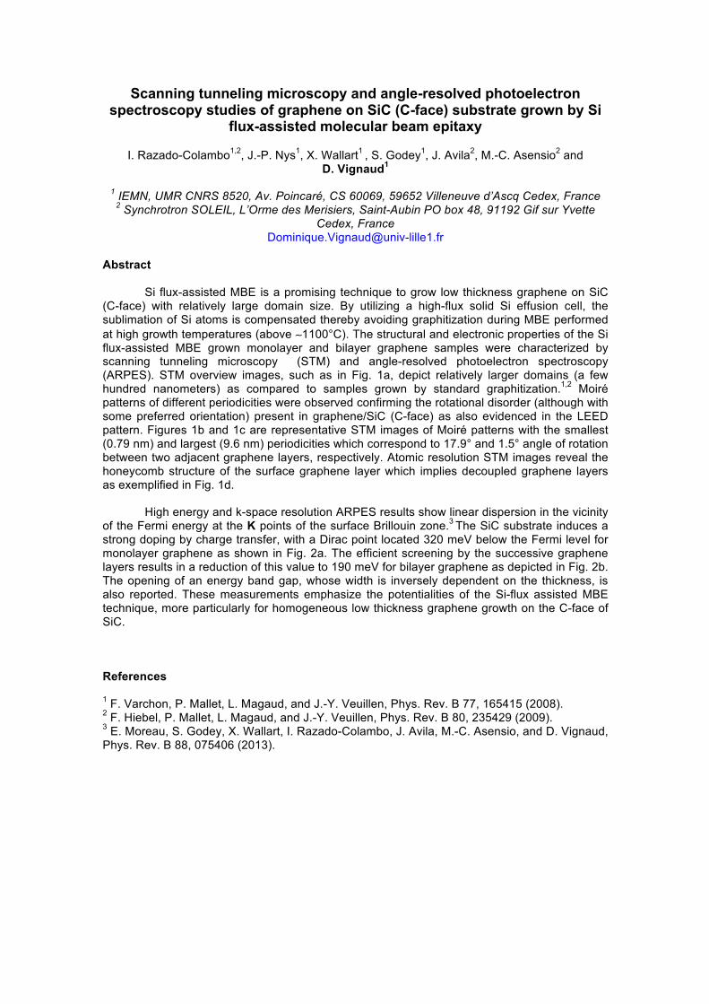
Scanning tunneling microscopy and angle-resolved photoelectron spectroscopy studies of graphene on SiC (C-face) substrate grown by Si
flux-assisted molecular beam epitaxy
I. Razado-Colambo1,2
, J.-P. Nys1, X. Wallart
1, S. Godey
1, J. Avila
2, M.-C. Asensio
2and
D. Vignaud1
1IEMN, UMR CNRS 8520, Av. Poincaré, CS 60069, 59652 Villeneuve d’Ascq Cedex, France
2Synchrotron SOLEIL, L’Orme des Merisiers, Saint-Aubin PO box 48, 91192 Gif sur Yvette
Cedex, [email protected]
Abstract
Si flux-assisted MBE is a promising technique to grow low thickness graphene on SiC (C-face) with relatively large domain size. By utilizing a high-flux solid Si effusion cell, the sublimation of Si atoms is compensated thereby avoiding graphitization during MBE performed
at high growth temperatures (above ∼1100°C). The structural and electronic properties of the Si flux-assisted MBE grown monolayer and bilayer graphene samples were characterized by scanning tunneling microscopy (STM) and angle-resolved photoelectron spectroscopy (ARPES). STM overview images, such as in Fig. 1a, depict relatively larger domains (a few hundred nanometers) as compared to samples grown by standard graphitization.
1,2Moiré
patterns of different periodicities were observed confirming the rotational disorder (although with some preferred orientation) present in graphene/SiC (C-face) as also evidenced in the LEED pattern. Figures 1b and 1c are representative STM images of Moiré patterns with the smallest (0.79 nm) and largest (9.6 nm) periodicities which correspond to 17.9° and 1.5° angle of rotation between two adjacent graphene layers, respectively. Atomic resolution STM images reveal the honeycomb structure of the surface graphene layer which implies decoupled graphene layersas exemplified in Fig. 1d.
High energy and k-space resolution ARPES results show linear dispersion in the vicinity of the Fermi energy at the K points of the surface Brillouin zone.
3The SiC substrate induces a
strong doping by charge transfer, with a Dirac point located 320 meV below the Fermi level for monolayer graphene as shown in Fig. 2a. The efficient screening by the successive graphene layers results in a reduction of this value to 190 meV for bilayer graphene as depicted in Fig. 2b.The opening of an energy band gap, whose width is inversely dependent on the thickness, is also reported. These measurements emphasize the potentialities of the Si-flux assisted MBE technique, more particularly for homogeneous low thickness graphene growth on the C-face of SiC.
References
1F. Varchon, P. Mallet, L. Magaud, and J.-Y. Veuillen, Phys. Rev. B 77, 165415 (2008).
2F. Hiebel, P. Mallet, L. Magaud, and J.-Y. Veuillen, Phys. Rev. B 80, 235429 (2009).
3E. Moreau, S. Godey, X. Wallart, I. Razado-Colambo, J. Avila, M.-C. Asensio, and D. Vignaud,
Phys. Rev. B 88, 075406 (2013).
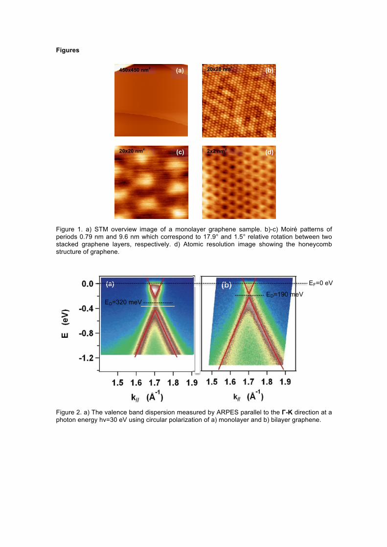
Figures
Figure 1. a) STM overview image of a monolayer graphene sample. b)-c) Moiré patterns of periods 0.79 nm and 9.6 nm which correspond to 17.9° and 1.5° relative rotation between two stacked graphene layers, respectively. d) Atomic resolution image showing the honeycomb structure of graphene.
Figure 2. a) The valence band dispersion measured by ARPES parallel to the Γ-K direction at aphoton energy hν=30 eV using circular polarization of a) monolayer and b) bilayer graphene.
EF=0 eV
ED=190 meV
ED=320 meV
(a) (b)
(c) (d)
450x450 nm2 20x20 nm
2
20x20 nm2
2x2 nm2
!
Elementary processes and factors influencing the intercalation between graphene and iridium
Sergio Vlaic1,2
, Amina Kimouche1,2
, Johann Coraux1,2
, Benito Santos3, Andrea Locatelli
3,
Nicolas Rougemaille1,2
1Univ. Grenoble Alpes, Inst. NEEL, F38042 Grenoble, France
2CNRS, Inst NEEL, F-38042 Grenoble, France
3Elettra – Sincrotrone Trieste S.C.p.A., S.S. 14 km 163.5 in Area Science Park, I-34149 Basovizza,
Trieste, [email protected]
Abstract
Besides their potential for mass production of graphene, epitaxial graphene systems make it possible to manipulate graphene’s properties and to induce new ones, in a finely controlled manner, by nanostructuring, defect engineering, strain engineering, and intercalation. The latter consists of inserting foreign species between graphene and its substrate and has attracted a great deal of attention since the last 5 years. It has allowed one, for instance, to fully decouple graphene from its substrate (H intercalation [1]), to spin-polarize graphene’s electronic bands (Au intercalation [2]), and to manipulate the ferromagnetism of an intercalated Co layer [3].Even though intercalation has been known since the 1980’s, it has only been recent that pathways explaining how intercalation initiates have been pursued. To date only a few have been identified: graphene edges [4] and pre-existing point defects, on flat graphene regions [5] as well as at the intersection between graphene wrinkles (linear delamination of graphene from its substrate) [6].Real time monitoring of the intercalation of cobalt between graphene and Ir(111) with the help of low-energy electron microscopy (LEEM), has provided us with greater insight. We discovered unanticipated intercalation pathways, unveiled the processes energetics and how both depend on the graphene-substrate interaction. More specifically, we found that intercalation does not require the pre-existence of point defects inside the graphene lattice to proceed, but can occur at curved regions, such as those found at graphene wrinkles and on top of substrate step edges (Fig.1 a) and b)) [7]. Curved region intercalation is found to be in competition with edge intercalation (Fig. 1 c)). We show that these two processes and their relative occurrence can be controlled by temperature and the interaction of graphene with the substrate [7-8].
References
[1] C. Riedl, C. Coletti, T. Iwasaki, A. A. Zakharov, and U. Starke, Phys. Rev. Lett. 103, (2009), 246804.[2] A. Varykhalov, J. Sanchez-Barriga, A. M. Shikin, C. Biswas, E. Vescovo, A. Rybkin, D. Marchenko,
and O. Rader, Phys. Rev. Lett. 101, (2008), 157601.[3] N. Rougemaille, A.T. N’Diaye, J.Coraux, C. Vo-Van, O. Fruchart, and A. K. Schmid, Appl. Phys. Lett.
101, (2012), 142403. J. Coraux, A. T. NDiaye, N. Rougemaille, C. Vo-Van, A. Ki- mouche, H.-X. Yang, M. Chshiev, N.Bendiab, O. Fruchart, and A. K. Schmid, J. Phys. Chem. Lett. 3, (2012), 2059.
[4] P. Sutter, J. T. Sadowski, and E. A. Sutter, J. Am. Chem. Soc. 132, (2010), 8175.[5] M. Sicot, P. Leicht, A. Zusan, S. Bouvron, O. Zander, M. Weser, Y. S. Dedkov, K. Horn, and M.
Fonin, ACS Nano 6, (2012), 151.[6| M. Petrović, I. Šrut Rakić, S. Runte, C. Busse, J. T. Sadowski, P. Lazić, I. Pletikosić, Z.-H. Pan, M.
Milun, P. Pervan, N. Atodiresei, R. Brako, D. Šokčević, T. Valla, T. Michely and M. Kralj, Nat.Commun. 4, (2013) 2772.
[7] S. Vlaic, A. Kimouche, J. Coraux, B. Santos, A. Locatelli, N. Rougemaille, under review.[8] S. Vlaic, A. Kimouche, J. Coraux, B. Santos, A. Locatelli, N. Rougemaille, submitted.

Figure
Figure 1: Schematic representation (left) and LEEM image (right) of Co intercalation between graphene and Ir(111) at the substrate step edges (a), at graphene wrinkles (b) and at the graphene free edges (c).Darker areas under the graphene sheet represent the intercalation regions.
Tunable, Ultralow-Power Switching in Memristive Devices Enabled by Graphene-Oxide
Heterogeneous Interface
Xinran Wang, Min Qian, Yiming Pan, Fengyuan Liu, Miao Wang, Haoliang Shen, Daowei He, Baigeng
Wang, Yi Shi and Feng Miao
Nanjing University, Nanjing 210093, China [email protected]
The application of graphene in electronics has been a widely anticipated yet very challenging goal.
Especially, the lack of bandgap hinders its use as logic transistors. On the other hand, graphene has a
unique property that the Fermi energy can be tuned in a wide range due to low density of states (DOS)
near the Dirac points. When forming heterostructures with other materials, the interfacial barrier height
can be tuned by gating, leading to many novel devices such as tunneling transistors with high on/off
ratio, barristors, and photodetectors. One of the intrinsic limitations of these heterogeneous devices is
the low drive current, partly due to the low DOS of graphene that inhibits efficient carrier injection. This
is unfavorable for high-performance logic transistors, but could be favorable in information storage,
where low energy operation (reading and writing) is attractive.
In this talk, we will present our recent works on the resistive memory applications of graphene
heterostructures.[1]
We integrate large-area CVD graphene into TiOx-based memristive devices to
realize ultralow switching power and non-linear I-V characteristics simultaneously. Compared to
conventional Pt-based memristive devices (PtMD), graphene-based ones (GMD) show a significant
switching power reduction up to ~880 times. In addition, GMD do not sacrifice other merits such as
memory window, endurance and retention. We find that the interface between graphene and TiOx plays
a dominant role in device switching and therefore offers a unique playground to engineer memory
characteristics. Such tunability can be realized by the quality and Fermi energy of graphene, which is
not possible in conventional metal/oxide/metal structures. Finally, flexible and transparent GMD are
demonstrated on Poly(ethylene naphthalate) (PEN) and show excellent retention against mechanical
bending. The extra-low switching current down to 1 and high resistance in our GMD is especially
interesting in computing applications, such as neuromorphic applications, where huge parallelism
requires very low leakage currents and thus high device resistance.
References
[1] Min Qian, Yiming Pan, Fengyuan Liu, Miao Wang, Haoliang Shen, Daowei He, Baigeng Wang, Yi
Shi *, Feng Miao* and Xinran Wang* Tunable, Ultralow-Power Switching in Memristive Devices
Enabled by Graphene-Oxide Heterogeneous Interface

Figures
Figure caption: (a) Switching curves of a typical GMD (blue) and PtMD (red) with 5µA and 3mA SET
current compliance respectively. The arrows point to the switching directions. Inset shows small bias I-V
curves for both devices at ON state, showing significantly different resistance. (b) Resistance versus
switching power of 20 different GMD and PtMD. Triangles denote RON and the corresponding PRESET,
while crosses denote ROFF and the corresponding PSET. Blue: GMD; red: PtMD.
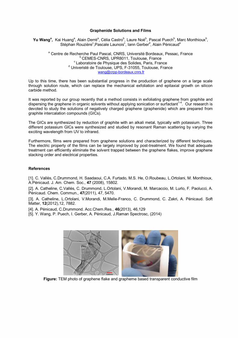
Graphenide Solutions and Films
Yu Wanga, Kai Huang
a, Alain Derré
a, Célia Castro
b, Laure Noé
b, Pascal Puech
b, Marc Monthioux
b,
Stéphan Rouzièrec,Pascale Launois
c, Iann Gerber
d, Alain Pénicaud
a
a Centre de Recherche Paul Pascal, CNRS, Université Bordeaux, Pessac, France
b CEMES-CNRS, UPR8011, Toulouse, France
c Laboratoire de Physique des Solides, Paris, France
d Univeristé de Toulouse, UPS, F-31055, Toulouse, France
Up to this time, there has been substantial progress in the production of graphene on a large scale through solution route, which can replace the mechanical exfoliation and epitaxial growth on silicon carbide method. It was reported by our group recently that a method consists in exfoliating graphene from graphite and dispersing the graphene in organic solvents without applying sonication or surfactant
1-4. Our research is
devoted to study the solutions of negatively charged graphene (graphenide) which are prepared from graphite intercalation compounds (GICs). The GICs are synthesized by reduction of graphite with an alkali metal, typically with potassium. Three different potassium GICs were synthesized and studied by resonant Raman scattering by varying the exciting wavelength from UV to infrared. Furthermore, films were prepared from graphene solutions and characterized by different techniques. The electric property of the films can be largely improved by post-treatment. We found that adequate treatment can efficiently eliminate the solvent trapped between the graphene flakes, improve graphene stacking order and electrical properties.
References
[1]. C. Vallés, C.Drummond, H. Saadaoui, C.A. Furtado, M.S. He, O.Roubeau, L.Ortolani, M. Monthioux, A.Pénicaud. J. Am. Chem. Soc., 47 (2008), 15802.
[2]. A. Catheline, C.Vallés, C. Drummond, L.Ortolani, V.Morandi, M. Marcaccio, M. Lurlo, F. Paolucci, A. Pénicaud. Chem. Commun., 47(2011), 47, 5470.
[3]. A. Catheline, L.Ortolani, V.Morandi, M.Melle-Franco, C. Drummond, C. Zakri, A. Pénicaud. Soft Matter, 12(2012),12, 7882.
[4]. A. Pénicaud, C.Drummond. Acc.Chem.Res., 46(2013), 46,129 [5]. Y. Wang, P. Puech, I. Gerber, A. Pénicaud, J.Raman Spectrosc, (2014)
Figure: TEM photo of graphene flake and grapheme based transparent conductive film
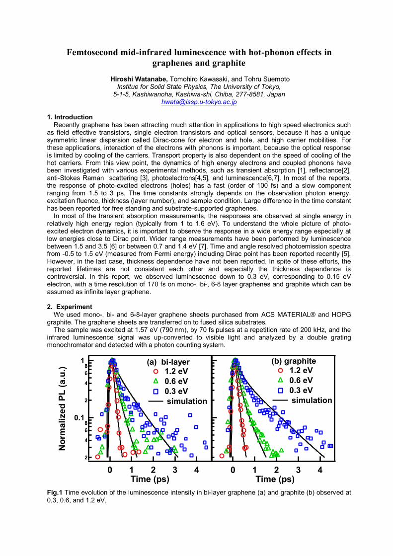
Femtosecond mid-infrared luminescence with hot-phonon effects in
graphenes and graphite
Hiroshi Watanabe, Tomohiro Kawasaki, and Tohru Suemoto Institue for Solid State Physics, The University of Tokyo,
5-1-5, Kashiwanoha, Kashiwa-shi, Chiba, 277-8581, Japan [email protected]
1. Introduction
Recently graphene has been attracting much attention in applications to high speed electronics such as field effective transistors, single electron transistors and optical sensors, because it has a unique symmetric linear dispersion called Dirac-cone for electron and hole, and high carrier mobilities. For these applications, interaction of the electrons with phonons is important, because the optical response is limited by cooling of the carriers. Transport property is also dependent on the speed of cooling of the hot carriers. From this view point, the dynamics of high energy electrons and coupled phonons have been investigated with various experimental methods, such as transient absorption [1], reflectance[2], anti-Stokes Raman scattering [3], photoelectrons[4,5], and luminescence[6,7]. In most of the reports, the response of photo-excited electrons (holes) has a fast (order of 100 fs) and a slow component ranging from 1.5 to 3 ps. The time constants strongly depends on the observation photon energy, excitation fluence, thickness (layer number), and sample condition. Large difference in the time constant has been reported for free standing and substrate-supported graphenes.
In most of the transient absorption measurements, the responses are observed at single energy in relatively high energy region (typically from 1 to 1.6 eV). To understand the whole picture of photo-excited electron dynamics, it is important to observe the response in a wide energy range especially at low energies close to Dirac point. Wider range measurements have been performed by luminescence between 1.5 and 3.5 [6] or between 0.7 and 1.4 eV [7]. Time and angle resolved photoemission spectra from -0.5 to 1.5 eV (measured from Fermi energy) including Dirac point has been reported recently [5]. However, in the last case, thickness dependence have not been reported. In spite of these efforts, the reported lifetimes are not consistent each other and especially the thickness dependence is controversial. In this report, we observed luminescence down to 0.3 eV, corresponding to 0.15 eV electron, with a time resolution of 170 fs on mono-, bi-, 6-8 layer graphenes and graphite which can be assumed as infinite layer graphene. 2. Experiment
We used mono-, bi- and 6-8-layer graphene sheets purchased from ACS MATERIAL® and HOPG graphite. The graphene sheets are transferred on to fused silica substrates.
The sample was excited at 1.57 eV (790 nm), by 70 fs pulses at a repetition rate of 200 kHz, and the infrared luminescence signal was up-converted to visible light and analyzed by a double grating monochromator and detected with a photon counting system.
Fig.1 Time evolution of the luminescence intensity in bi-layer graphene (a) and graphite (b) observed at 0.3, 0.6, and 1.2 eV.
43210Time (ps)
(b) graphite1.2 eV
0.6 eV
0.3 eV
simulation
2
4
6
80.1
2
4
6
81
No
rmali
zed
PL
(a.u
.)
43210Time (ps)
(a) bi-layer1.2 eV
0.6 eV
0.3 eV
simulation

3. Results and Discussion Photon energy dependences of the decay profiles in
bi-layer graphene and graphite under relatively high excitation fluence (100 mW) are shown in Fig. 1(a) and (b), respectively. In graphite, the lifetime becomes longer at lower photon energy as reported in ref. [8]. In the case of bi-layer graphene, however, the lifetime at 0.3 eV is not so long as that in graphite, while the lifetime at 1.2 eV is almost the same. Elongation of the lifetime at lower energy is ascribed to slower decay of electron population at lower energy, as predicted by Fermi-Dirac distribution assuming cooling down of the electron system via optic phonons. Luminescence signals from graphenes with different thickness are shown in Fig. 2. At the lowest energy 0.3 eV, the thickness dependence is most clearly seen, that is, the lifetime in mono-layer graphene is roughly one half of that in graphite, while that of 6-8 sample is almost the same as that of graphite.
We try to understand these observation in terms of the two-temperature model [7]. We assume that the energy of the electron system is transferred to the
optic phonon (G mode, op = 0.2 eV) as the first step and that the energy of the hot optic phonon is
dissipated to the large heat bath within the graphene sheet. We can derive the differential equations for the energy of electron Ue and optical phonon UOP.
,where G(t) is the envelop of pulse shape Te, TOP, and TRT are electron temperature, optical phonon temperature, and temperature of the heat bath (TRT = 300 K), COP is the heat capacity of the optical phonon, De is the density of state of electron, and fe is the Dirac-Fermi function at Te.
The calculated curves for graphite are shown in Fig. 1(b) by solid lines, which are in good agreement with experiment. Then the fast decays in bi-layer graphene are reproduced simply by adding a path from the optic phonons of the graphene or graphite to the optic phonons of the substrate, having an infinite heat capacity as shown in Fig. 1(a). This suggests that the interaction between the hot carriers and the substrate is the main cooling mechanism in silica-supported graphene as proposed in ref. [3]. References [1] Bo Gao et al., Nano Lettres 11, 3184 3189 (2011). [2] P. J. Hale, S. M. Hornett, J. Moger, D. W. Horsell, and E. Hendry Phys. Rev. B 83 121404-1-4 (2011). [3] Shiwei Wu et al. Nano Letters 12, 5495-5499 (2012). [4] J. C. Johannsen et al. Phys. Rev. Lett. 111, 027403-1-5 (2013) [5] I. Gierz et al. Nat. Materials, 12, 1119-1124 (2013). [6] C. H.Lui, K. F.Mak, J.Shan, and T. F. Heinz, Phys. Rev. Lett. 105, 127404-1-4 (2010). [7] T. Koyama et al. ACS NANO 7, 2335 2343 (2013). [8] T. Suemoto, S. Sakaki, M. Nakajima, Y. Ishida, and S. Shin Phys. Rev. B 87, 224302-1-5 (2013).
Fig. 2 Thickness dependence of the luminescence decay profiles observed at 0.3 eV. Data for 1, 2 and 6-8 layers graphene and for graphite are shown.
0.1
1
10
100
PL
In
ten
sit
y (
a.
u.)
3210
Delay time (ps)
graphite
6~8 layers
2 layers
graphene
0.3 eV(b)
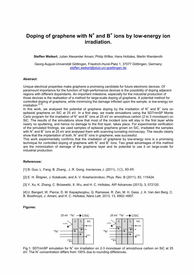
Doping of graphene with N+ and B
+ ions by low-energy ion
irradiation.
Steffen Weikert, Julian Alexander Amani, Philip Willke, Hans Hofsäss, Martin Wenderoth
Georg-August-Universität Göttingen, Friedrich-Hund-Platz 1, 37077 Göttingen, Germany
Abstract: Unique electrical properties make graphene a promising candidate for future electronic devices. Of paramount importance for the function of high-performance devices is the possibility of doping adjacent regions with different dopandants. An important milestone, especially for the industrial production of those devices is the realisation of a method for large-scale doping of graphene. A potential method for controlled doping of graphene, while minimizing the damage inflicted upon the sample, is low-energy ion irradiation
[2-4].
In this work, we analysed the potential of graphene doping by the irradiation of N+ and B
+ ions on
epitaxial graphene on SiC at 25 eV. In a first step, we made simulations using the SDTrimSP Monte Carlo program for the irradiation of N
+ and B
+ ions at 25 eV on amorphous carbon (2 to 3 monolayer) on
SiC. The results of the simulations show that most of the incident ions will stay in the first layer while nearly no sputtering, and hence no damage to the first layer, takes place. For experimental verification of the simulated findings, we used samples of epitaxial graphene grown on SiC, irradiated the samples with N
+ and B
+ ions at 25 eV and analysed them with scanning tunneling microscopy. The results clearly
show that the implantation of both, N+ and B
+ ions in graphene, was successful.
This work experimentally confirms that the irradiation of graphene by low-energy ions is a promising technique for controlled doping of graphene with N
+ and B
+ Ions. Two great advantages of this method
are the minimization of damage of the graphene layer and its potential to use it on large-scale for industrial production. References:
[1] B. Guo, L. Fang, B. Zhang , J. R. Gong, Insciences J. (2011), 1(2), 80-89.
[2] J. Kotakoski, and A. V. Krasheninnikov, Phys. Rev. B (2011), 83, 115424. [3] Y. Xu, K. Zhang, C. Brüsewitz, X. Wu, and H. C. Hofsäss, AIP Advances (2013), 3, 072120. [4] U. Bangert, W. Pierce, D. M. Kepaptsoglou, Q. Ramasse, R. Zan, M. H. Gass, J. A. Van den Berg, C. B. Boothroyd, J. Amani, and H. C. Hofsäss, Nano Lett. 2013, 13, 4902 4907. Figures:
Fig.1: SDTrimSP simulation for N
+ ion irradiation on 2-3 monolayer of amorphous carbon on SiC at 25
eV. The N+
concentration differs from 100% due to rounding differences.

Fig.2: SDTrimSP simulation for B+ ion irradiation on 2-3 monolayer of amorphous carbon on SiC at 25
eV. The N+
concentration differs from 100% as a result of rounding differences.
(a) (b)
(c) (d)
Fig.3: STM topography of epitaxial graphene grown on SiC doped with N
+ ions. The pictures (a) and (c)
show the same area at different voltages. The pictures (b) and (d) show a detail of the pictures (a) and (c), respectively.
Fig.4: STM topography of epitaxial graphene grown on SiC doped with B
+ ions. The pictures show
different resolutions of the same sample.
3 nm 2 nm
1 nm 0.5 nm
Industrial Scale Graphene Oxide Production and Application
Sameer Fotedar1, Rune Wendelbo
1and Einar Eilertsen
2
1. Abalonyx AS, Forskningsveien 1, 0373 Oslo, Norway2. Kongsberg Innovation AS, Kirkegårdsveien 45, 3616 Kongsberg, Norway
An important high volume demand for graphene oxide (GO) is now emerging within the oil and gas
industry, creating an urgent need for industrial scale production. Abalonyx has already in 2012
developed and verified a production process1
which is now being scaled up further in collaboration with
Kongsberg Innovation in Norway. An annual capacity of 8 tons is targeted to be reached this year,
aiming at an annual production of 1000 tons in 2016.
Graphene Oxide is traditionally prepared by the method of Hummers and Offemann2, but with the recent
interest in graphene and graphene derivatives, several modifications of the method of Hummers and
Offeman, as well as novel methods have been announces. The Abalonyx process has been developed
with focus on safety, environmental sustainability, scalability and cost efficiency.
The Abalonyx process has been optimized in order to avoid formation of toxic fumes and to minimize
waste. In the first stage, a 1 Kg batch reactor will be set up, followed by a 6 Kg batch reactor. The 6 Kg
batch reactor will be fully automated to be run 4 cycles per 24 h. The end product is an aqueous 30 %
GO-paste that can safely be stored and transported.
References
[1] R. Wendelbo and S. Fotedar. Norwegian patent application No. 20121709.
[2] W. S. Hummers and R. E. Offemann, J. Am. Chem. Soc., 1958, 80 (6), pp 1339 1339

Reduced Graphene Oxide Decoration with Ffunctional Nano-crystals
Rune Wendelbo1, Sameer Fotedar
1and Volodymyr Yartys
2
1. Abalonyx AS, Forskningsveien 1, 0373 Oslo, Norway2. IFE, Instituttveien 18, 2007 Kjeller, Norway
Reduced Graphene Oxide (rGO) is a potentially cheap graphene derivative with several attractive
properties such as high specific surface area, good electric conductivity and low reactivity. These
properties make rGO an attractive support for catalysts, solar cells materials and other functional
materials in nano-size. Not only is the combination of a second phase on graphene potentially
interesting, but nucleation and subsequent growth of the second phase on the surface of graphene can
induce novel properties that cannot normally be obtained, in particular in terms of size and shape as
well as transport of electrons to and from the second phase, exemplified for perovskites1. The practical
potential has already been reported for photocatalysts2
and solar cells3
We present here the wet chemical, hydrothermal deposition of CaCO3, CuO, perovskite, zeolite and
ZnO on rGO demonstrating the wide range of possibilities with this approach. In the two examples
shown below, nano-CaCO3 coats the rGO-surface in Fig.1 whereas nano-CuO appears as discrete
particles in Fig.2.
Abalonyx is presently scaling up its GO production process4
to a target capacity of 8 t/y by year-end.
The availability of abundant GO at a low price is mandatory for commercialization of products based on
GO and rGO.
Fig.1. Nano-crystals of CaCO3 on rGO. Fig.2. CuO nano-crystals on RGO.
References[1] R. Wendelbo et al., A, 2006. J. Eur. Ceramic Soc. 26 (6) pp 849-859[2] G. Williams et al. ACS Nano, 2008, 2 (7), pp 1487 1491
[3] R J. Tse-Wei Wang et al. Nano Letters, 2013; 1021/nl403997a[4] R. Wendelbo and S. Fotedar. Norwegian patent application No. 20121709
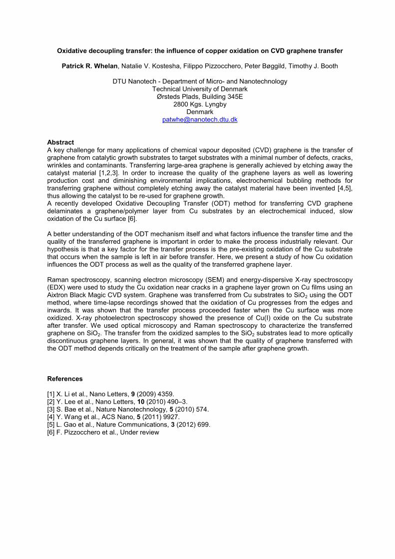
Oxidative decoupling transfer: the influence of copper oxidation on CVD graphene transfer
Patrick R. Whelan, Natalie V. Kostesha, Filippo Pizzocchero, Peter Bøggild, Timothy J. Booth
DTU Nanotech - Department of Micro- and Nanotechnology Technical University of Denmark
Ørsteds Plads, Building 345E 2800 Kgs. Lyngby
Denmark [email protected]
Abstract A key challenge for many applications of chemical vapour deposited (CVD) graphene is the transfer of graphene from catalytic growth substrates to target substrates with a minimal number of defects, cracks, wrinkles and contaminants. Transferring large-area graphene is generally achieved by etching away the catalyst material [1,2,3]. In order to increase the quality of the graphene layers as well as lowering production cost and diminishing environmental implications, electrochemical bubbling methods for transferring graphene without completely etching away the catalyst material have been invented [4,5], thus allowing the catalyst to be re-used for graphene growth. A recently developed Oxidative Decoupling Transfer (ODT) method for transferring CVD graphene delaminates a graphene/polymer layer from Cu substrates by an electrochemical induced, slow oxidation of the Cu surface [6]. A better understanding of the ODT mechanism itself and what factors influence the transfer time and the quality of the transferred graphene is important in order to make the process industrially relevant. Our hypothesis is that a key factor for the transfer process is the pre-existing oxidation of the Cu substrate that occurs when the sample is left in air before transfer. Here, we present a study of how Cu oxidation influences the ODT process as well as the quality of the transferred graphene layer. Raman spectroscopy, scanning electron microscopy (SEM) and energy-dispersive X-ray spectroscopy (EDX) were used to study the Cu oxidation near cracks in a graphene layer grown on Cu films using an Aixtron Black Magic CVD system. Graphene was transferred from Cu substrates to SiO2 using the ODT method, where time-lapse recordings showed that the oxidation of Cu progresses from the edges and inwards. It was shown that the transfer process proceeded faster when the Cu surface was more oxidized. X-ray photoelectron spectroscopy showed the presence of Cu(I) oxide on the Cu substrate after transfer. We used optical microscopy and Raman spectroscopy to characterize the transferred graphene on SiO2. The transfer from the oxidized samples to the SiO2 substrates lead to more optically discontinuous graphene layers. In general, it was shown that the quality of graphene transferred with the ODT method depends critically on the treatment of the sample after graphene growth. References [1] X. Li et al., Nano Letters, 9 (2009) 4359. [2] Y. Lee et al., Nano Letters, 10 (2010) 490 3. [3] S. Bae et al., Nature Nanotechnology, 5 (2010) 574. [4] Y. Wang et al., ACS Nano, 5 (2011) 9927. [5] L. Gao et al., Nature Communications, 3 (2012) 699. [6] F. Pizzocchero et al., Under review
Figures
Figure 2: Optical images of graphene on SiO2 after transfer. Insets show Raman spectrum from sample.
Oxidized Not oxidized Slightly oxidized
Figure 1: SEM images of graphene on Cu films after growth. Cu grain boundaries and ridges/cracks in the graphene layer are clearly visible. The presence of copper oxide can be seen as the dark areas around graphene cracks and some oxidized areas are pointed out by white arrows.
Insets show oxygen content determined by EDX.
Oxidized Slightly oxidized Not oxidized
EDX oxygen content: 2.5% EDX oxygen content: 1.5% EDX oxygen content: 0%


Photophysical Interactions of Phthalocyanines with Graphene Nanosheets
Leonie Wibmer,a Leandro M. O. Lourenço,a,b Alexandra Roth,a Georgios Katsukis,a Tomás Torres,c Dirk M. Guldia
a Department of Chemistry and Pharmacy and Interdisciplinary Center for Molecular Materials, Friedrich-Alexander-
University Erlangen-Nuremberg, 91058 Erlangen, Germany
b QOPNA and Department of Chemistry, University of Aveiro, 3810-193 Aveiro, Portugal
c Department of Organic Chemistry, Autonoma University of Madrid, Cantoblanco, 28049 Madrid, Spain
Graphene, an one-atom-thick two-dimensional material, is attracting more and more interest since the pioneering work by Novoselov et al. in 2004.[1] It has outstanding properties like, for example, transparency, high electrical and thermal conductivity, and extreme mechanical strength and elasticity [2], which render it a promising material, for example, for solar cells.[3]
In the current work, a top-down approach to produce graphene flakes, namely liquid phase exfoliation of graphite is used. Hereby, several different phthalocyanines are investigated with regard to their ability to exfoliate graphite, on one hand, and to stabilize as well as to interact with the resulting graphene flakes, on the other hand. Ground and excited state features of these reference systems were probed by means of absorption and fluorescence spectroscopy.
The preparation of stable graphene hybrids followed several enrichment cycles, comprising the addition of natural graphite to a phthalocyanine solution, ultrasonification, and subsequent centrifugation of the suspensions. Hereby, the - interactions between the phthalocyanines and the basal plane of graphene stabilize the exfoliated graphene flakes. Raman, TEM, and AFM analyses reveal that the newly formed electron donor-acceptor hybrids coexist upon drop casting as large few-layer graphene and turbostratic exfoliated graphite flakes as well as smaller monolayer graphene. In the resulting hybrids, electronic coupling is seen in the form of newly appearing absorption features and an almost complete quenching of the original phthalocyanine centered fluorescence. The aforementioned was complemented by femtosecond pump probe spectroscopy, which corroborated that the electronic coupling between the phthalocyanines, on one hand, and graphene, on the other hand, is accompanied by ultrafast charge transfer processes.[4-5]
References [1] K. S. Novoselov, A. K. Geim, S. V. Morozov, D. Jiang, Y. Zhang, S. V. Dubonos, I. V. Grigorieva, A. A. Firsov, Science (2004) 306, 666-669. [2] K. S. Novoselov, V. I. Fal'ko, L.Colombo, P. R. Gellert, M. G. Schwab, K. Kim, Nature (2012) 490, 192-200. [3] M. A. Gluba, D. Amkreutz, G. V. Troppenz, J. Rappich, M. H. Nickel, Appl. Phys. Lett. (2013) 103, 073102. [4] R. D. Costa, J. Malig, W. Brenner, N. Jux, D. M. Guldi, Adv. Mater. (2013) 25, 2600-2605. [5] J. Malig, D. Jux, D. Kiessling, J-J. Cid, P. Vázquez, T. Torres, D.M. Guldi, Angew. Chem. (2011) 50, 3561.

Figures
Figure 1: Electronic coupling between the phthalocyanine and graphene is established by new arising absorption features (left) and a complete quenching of the phthalocyanine centered fluorescence (right) during the enrichment procedure.
Klein-tunneling transistor with ballistic graphene
Quentin Wilmart1, Salim Berrada2, V. Hung Nguyen2, Gwendal Feve1,
Jean-Marc Berroir1, Philippe Dollfus2, Bernard Placais1
1 Laboratoire Pierre Aigrain, Ecole Normale Superieure, CNRS (UMR 8551), Universite P. et M. Curie,
Universite D. Diderot, 24, rue Lhomond, 75231 Paris Cedex 05, France2 Institute of Fundamental Electronics, Univ. Paris-Sud, CNRS, Orsay, France
Abstract
Today the availability of high mobility graphene up to room temperature makes ballistic transport in
nanodevices achievable. In particular, p-n-p transistors in the ballistic regime give access to the Klein
Tunneling (KT) physics and allow the realization of devices exploiting the optics-like behavior of Dirac
Fermions (DF) as in the Vesalego lens or the Fabry Perot cavity [1, 2, 3]. New electronic architectures
based on Klein tunneling open the way to applications, especially in microwave electronics where both
high mobility and a switching capability are needed to achieve large voltage and power gain at high
frequency.
Our device exploits the total internal reflection in a KT prism (see figure 1) [4] which leads to the
tunable suppression of the transistor transmission. The prism is made of an n-doped ballistic triangular
domain embedded in a p-doped diffusive area, both domains being controlled electrostatically. Alike in
light reflectors, an array of KT-prisms can be used to form the active channel of a KT transistor (see figure
2); this geometry minimizes the gate length to keep ballistic transport conditions. The behavior of the KT
transistor is calculated by scattering theory as well as atomistic simulations using the non equilibrium
Green function (NEGF). Both approaches predict for the Klein tunneling transistor a strong suppression
of conductance at large gate doping that can eventually drop below the minimum conductance at charge
neutrality. This KT transistor can be used as a tunable barrier for electrostatic quantum confinement to
achieve, e.g. single Dirac fermion pumps working at low temperatures. It is also suited for microwave
electronics as it cumulates significant resistance in the OFF state with a large conductance in the ON
state.
In this talk I will describe the implementation of such a KT transistor, and the possibility to realize it
by depositing graphene onto local bottom gates and a few layers of hexagonal boron nitride (hBN). The
use of hBN as a dielectric gives access to ballistic transport in the device while keeping a good gate
coupling suitable for the realisation of abrupt p-n junctions. Those elements are essential to enter the
regime of DF optics where refraction and transmission at p-n junctions are determined by Fresnel-like
relations.
References
[1] M. I. Katnelson, K. S. Novoselov, A. K. Geim, Nat. Phys. 2, 620 (2006), Chiral tunnelling and the
Klein paradox in graphene
[2] A. F. Young, P. Kim, Nat. Phys. 5, 222 (2009), Quantum interference and Klein tunnelling in graphene
heterojunctions
[3] P. Rickhaus, R. Maurand, M-H. Liu, M. Weiss, K. Richter & C. Schoenenberger, Nat. Comm. 4, 2342
(2013), Ballistic interferences in suspended graphene
1

[4] Q. Wilmart, S. Berrada, D. Torrin, V. Hung Nguyen, G. Feve, J.M. Berroir, P. Dollfus, B. Placais, To
be published (2014), Klein-tunneling transistor with ballistic graphene
http://www.phys.ens.fr/~placais/publication/2014_2DM_Wilmart_KT_transistor_submit.
Figures
Figure 1: Principle of total reflection in a Klein tunneling prism. The refraction angle of Dirac fermion
(DF) beams (red rays) and their angular dependent transmission amplitude (blue lobes) are controlled
by the optical-like index ratio n = −
√
n/p of the p and n regions. a) OFF state n ≫ p. Anisotropic
forward scattering occurs at p-n junction : the refracted rays are mostly transmitted along the junction
normal within a lobe limited by |θ1| < θc. The n-p junction selects the incident carriers that are close
to the normal to the junction (i.e. |φ2| < φc); other being reflected. b) ON state n ≃ p. In this case
θc = φc = 90deg which means all indent rays are transmitted with large transmission coefficient at both
interfaces.
Figure 2: Artist view of graphene transistors, with a standard rectangular bottom gate (left), and with a
prismatic bottom gate (right).
2
������������������ ����������������������������������������������� ��
������������� �������������������� ��������������������������������� �� ��������!���"#����$�!�� �%�� ��������������&�������
����������������'(����$�� ������)����������*������ �+���� ��(��,�-������'(���� ./0�12��3������'����������)����������,�4�( �� ��*���� ��(�����5����'(���� 67/�78�9�!���'�������
����������: ��������+���� ��(��,�:�������:� /;<�%�(!����!��:������
�������=������� > �
�����
-�� � ��� ��'���� � �, � ��� � *��������� ?����'� � @*?� � ���������� ��� � �, � @��(���'� ����������� � �����A��� �'�������� ��,�,�������������������,�������������������,�3�������B������,,����-�� � ��� >�+ �'�*?���� �� � �� ���� � �� � '�� � � �'�� � ��� � ,�������� � ������� � �������' � � � '������ � ��� � �������� > � *?���� ������ � ��� � ���,����� � ,��� �<< �C � �� � 8;; �C � � � '������ ���� �������� � � � ����� � �� � ����� � ��������������������������,�������'�����������'������>�
� �����������������A��� �'������� � �'���� � �� �����"���� ���� ���� �*?)� ������� ��� �/.;;�*���� � � � ���������������������(���'�����7;;�*���������(�� �A� ������ ����������(����� ����.� ��*� �� ����� > �D,��� � '������ � '������ � ��� � ��������� � �������� � ��� � ,��������� � � � �����A��� � '������ � � �' � ������ � ����������� � ����� �' � �����E�� > � B�� � ��� � ��� � �������� � � ���������� � ���� ���� � � � �, � ���������� ����������>�)�������������� �������'� ���������������������������������A��������,�0����,�D������ ������������� ��� >�-�������� ���,���� �������� ����� ������������������� ��(� ������(���,���D������9�(�� �)��� �����@D9)���,�D��������A������'�������F/G>�$�A���������!�0;���D�0�8���(���� �'��������D9)>�B�������D9)�'������-������(� D�������� ��A���"����������� �������,��0;�������������������,�8;;�*>�$�A���� ����� �������� ��������D9)���(���� ����,���������������������������,������A���������,��������������!� ��, �H6;�>�-��� �����'������ ��'��� �����'������������ ��(���������� ���������!�'�������������,������� �F0G>�:������������ �������� ������� ��,����������������(������������A������*� ����� ������������ ������ �� �������� �����>
*?���� ������ ��������������D'���� ��.17;D�9*%��������� �/;;�!�"� � �� � ���������9�E��� �$����'���(� ���>�B�'����/� ��� �����*?��������!��� ���,�������,������������>�D�����������������������*?�������� �������������������������;�?������ ����'���������A���������������������� ��(��,� ���� �� �����������������)������������'�������F8�.�6G>�D ������������������ ������ ��������)��������������� ��� ����� ������� � �����A� ������, � ���� � � � �����A���> � �������� ��������� � � ��� ������ � � �������������������> � �*?���� ������ ����������*���,������ ����� ���,��������������'��,��'����������'��������D���������� ���������������� �� � �����(�����*?������� ��,��'����������'������� ����������� ������ �@B�'����8�> ����������������� ��A���������D�0�8�������� ��������������������<;;�*�F2G����������������,��������,�D9)�,��� �� �����������(������'����/;;;�*�,��� ����������� �F<G>�-������ ��������(��� �'�,������'����������'�� � � ����D����� �@���������� ���� � �� �'�� ������ ������������ �������(��� �"�������� �> � : � ���� ������� ������ ��������� ������������ ���(������������������A���>
D�����'�� ��� ���,�����'����������� ��� ������������'���������� ������ >�B����������������� ����� ���� ��������� ����������������������������,��������'������>�D ���� ��������� �����������������A���� �� � ��,���,�����)���������������'������� >�������� ��,���� ��� ���������� �����(���'����������� �������� > ������������� ��� �'�,�����,������� ��,��������D�0�8I��*� �������� �����������A��������������)����������� ���� �'�,�����(� ��,������D�0�8I'������� ����� �����'��������� �F<G>�-�� ������*?������������*������� �'��������������������'�����(�����������>�-��������������� ����������D9)�D�0�8�� ��,������E�����(>�B��������������������������������������*� ����� ������������������ �����,�����D9)�D�0�8���(���������� ������ ���������� ���J8>;> �%�'����� �� ��� � � � �� �������(� ���������������A��������������,�7 /;>�*����� ��� ������� ���������������� �����������������,�����D9)��(������'������'�������������>�:������� ������ � ���������,,�����,���'�������������������'��� ���� ������������'���������(�� >�
��������
F/G��>�C�����>���> �%����"������, �����'���������(����� '�����'�������,���� �,,���� ��� � ���������D�0�8�����������>�D���> �4�( >�9���>�1.�;20/;<�@0;;1�KF0G �5>�B������"�����>���> ������'��, �D�0�8������������ ,���'�������,���� �,,��� � ��� � ��� �D���>�4�( >�9���> �/;;�;18//0 �@0;/0�KF8G��>�L�����>���>���� ��������,�����E������������������,�'�������$������$���������'(�.��6;6� �6;1�@0;;1�KF.G�->�B�'���>���>�*������� ���� ��� ����E������������������,�'������� ���� ��������� >�D���>�4�( >�9���>�1/� �;10/;1�@0;;<�KF6G��>�)�� ���>�M���������������������� ��(��,� ���� ��,�'�������D���>�4�( >�9���>�12��/60/;.�@0;/;�KF2G��>�D����>���>��>��������� ��������B���������.78 .76�����<;6 <;7�@0;;.�KF<G��>�D����>���>��> ��������������������� ��, �D�0�8I.� ��*� �������� �'�����(����������(���������������������� ������>D���>�4�( >�/;0��;6.6/8�@0;;<�K�
B�'����/�@��,��N�*?���� ������ ���!��� ���,�������,�������������,����<<�C�@'��������8;;�C�@����>�D��<<�C ���������������������� ��� ������������;?��������'������A� ������,���)�����*��>�-��������������� ���� ������������� ������������������������������,����������.;;�O�>
B�'����0�@��'���N�*����������(�3?���� ������ ������� �� ������B�'����/>�D������������������� �� ����������;�?������������������'�� ������������� >�-�����'����������������� �����������'�����!�'�������'������D9)��A������(��>�
B�'����8�@��,��N�*?���� ������ �����*���,������ ����� ���!�����<<�C>�D������������ ��� ���������/;�? ��� ��������� >�-��������������������'����,������ ���� ���� ������������ �����,����'��,���������� ������ �����D�0�8>���� ������ �������!�����/;;�!�">
B�'����.�@��'���N �*����������(�3?������ � ��� ��� �� ���� � �B�'����8> �-������������� � ��� �������� ������ ��������(�� ��������� ���������� ��� ������������������������� ���,����!�'�������'�������A���> �

Graphene printing for flexible electronics
I. Wlasny1, M. Rogala
1, P. J. Kowalczyk
1, A. Busiakiewicz
1, W. Kozlowski
1, L. Lipinska
2, J. Jagiello
2,
M. Aksienionek2, W. Stupinski
2, P. Dabrowski
2, Z. Sieradzki
3, I. Krucinska
4, M. Puchalski
4,
E. Skrzetuska4, Z. Klusek
1
1 Department of Solid State Physics, Faculty of Physics and Applied Informatics, University of Lodz,
Pomorska 149/153, 90-236 Lodz, Poland 2 Institute of Electronic Materials Technology, Wolczynska 133, 01-919 Warsaw, Poland
3 Electrotechnological Company QWERTY Ltd., Siewna 21, 94-250 Lodz, Poland
4 Faculty of Material Technologies and Textile Design, Lodz University of Technology,
90-924 Lodz, Poland
Abstract The flexible electronics is recently attracting growing interest due to its large applicational potential. Among the methods used in the production of flexible electronic devices the inkjet and screen printing are popular as they allow for fast production of thin, conductive tracks on polymer foils or textile surfaces While nowadays various nanomaterials are used, the graphene might be very promising alternative for production of inks and pastes. The former might be replaced due to unique properties of the single graphitic sheets. The graphene is characterized by very high electrical and thermal conductivity. Furthermore it is very durable, flexible and transparent in the visible light spectrum. Those properties suggest it is an answer to the challenges set by modern flexible electronics and graphene might be used eg. for production of flexible touchscreens. Recently it has been shown that it is possible to use the graphene in the inkjet technology. The technology of manufacturing inks which use various forms of graphene are still in their early stage of development and they do not allow for commercial use. New ink compositions and printing methods need to be developed to fully exploit the unique properties of graphene for printed electronics and create flexible graphene-based overprints in controlled and repeatable. These challenges are subject of our current research. During our presentation we will show the prototype of the graphene-based printout, which was made using inkjet method on the flexible polymer foil. We will present the results of our macro- and nano-scale characterization of the morphology and the electrical resistivity which base among others on the measurments of the local conductivity with contact mode of the atomic force microscope. These results are confronted with the analysis of the chemical composition of the overprints and the ink investigated using X-ray photoemission spectroscopy. Furthermore, we point out potential problems and limitations of the graphene printing technology. We also focus on the problems which the technology will face during its commercialization. This work is supported by the National Centre for Research and Development under the project GRAF-TECH/NCBR/15/25/2013.

Study on Overlapping Graphene and InZnO Thin Film for Active layer of Transistor.
EunA Won1, Jihoon Jeon
1, Chansoo Yoon
1, Sangik Lee
1, Mijung Lee
1, Baeho Park
1
Department of physics, 120 neungdong-ro, Gwangjin-gu, seoul, korea
1
Abstract The fabrication of thin-film transistors based on amorphous silicon has been. Membrane process to create a simple and large-area amorphous silicon city, but does not apply to the display excellent electrical properties is difficult. Accordingly, the next generation of traffic register transparent transistors using oxide thin films and low-temperature grown spotlighted transparent oxide semiconductor prepared using a variety of transparent, flexible transistor applications is transparent, relatively high mobility and the possibility of low-temperature process, based on the characteristics transistor the application is possible. However, the mobility of the oxide thin film is limited. In this study, we will improve the mobility through the overlapping both of Oxide Thin Film and Transferred CVD Graphene[1]. ZnO, In2O3, SnO2 channel layer of a thin-film transistor manufacturing of Oxide-based and is mainly used for materials with better characteristics, and research continues. Transistor active layer InZnO thin films[2] by Spin-Coating Method and CVD Graphene as also active layer by transfer method using PMMA. Al as the electrode material, using a metal mask up manufacturing In this study, 20nm SiO2 layer on the top of the Si substrate to the electric arc furnace was changed by the following was Fabricated device, the electrical characteristics were measured using 4point probe ID-VD using Kethely 4156B transistor performance as measured by ID-VG measurements. References [1] Jinseong Heo, Nano Lett., 13, pp 5967 5971(2013). [2] Toshio Kamiya, Journal of Technology, 5(7), pp 273 288(2009). Figures
Electrode 2
Electrode 1
InZnO CVD Graphene
Si substrate Gate
SiO2
Au
Al
Overlap Area
Inverted Process Implementation of Monolithic Graphene Mixer
Hongming Lv, Huaqiang Wu*, He Qian
Institute of Microelectronics, Tsinghua University, Beijing, 100084, China [email protected]
Abstract
A monolithic graphene-based passive resistive FET mixer is implemented by a novel inverted process, which incorporates two routing layers and is implemented on 8 . The process is CMOS compatible with passive elements monolithically integrated. The mixer functionality is demonstrated at fRF=5.1GHz and fLO=5GHz. It features a conversion loss of -32dB at a fixed LO power PLO=0dBm.
Researchers have used individual graphene field-effect transistors (GFETs) connected to external
passive components to realize graphene circuits. Graphene monolithic integrated circuits, on the other
hand, could greatly expand graphene technological impacts. Pioneer researchers have made such
attempts. Lin et al. has demonstrated graphene circuits integrated on a single SiC wafer which opened
up the graphene integration possibility [1]. Han et al. moved forward by utilizing CVD graphene and
fabricated GHz-range graphene ICs in IBM 200 mm silicon fab [2].
Unlike conventional ICs in which field-effect transistors are formed on Si wafers with upper layers of
interconnect, this work proposes a novel inverted graphene integration approach. CMOS compatible
two-layer-routing technology on 8 wafer is utilized to form pre-patterned IC structures which include
inductors, interconnects, pads and buried GFET gate/source/drain regions. Afterwards, large-scale
monolayer graphene synthesized by CVD methods is transferred onto the pre-patterned dies to form
graphene ICs.
A thick SiO2 layer was first thermally grown on the 8-inch Si substrate, as shown in Fig. 1.
Passive components, four-turn inductors in this case, were formed in the first metal layer (500nm thick
Al) together with necessary interconnects. After interlayer passivation ( SiO2), the second metal
layer (500nm thick Al) was utilized to define GFET gate/source/drain regions, which enabled an
additional layer of interconnects. Chemical-Mechanical Polishing (CMP) was introduced to ensure the
planarization of the fabricated wafer. The GFET employs a two-finger structure with W/L dimension of
. 3.8 nm thick HfO2 (EOT 1nm) was deposited to form the gate dielectric by atomic layer
deposition (ALD) method. Buried source/drain regions were exposed, which formed graphene
source/drain contacts in the following steps.
Graphene was transferred to patterned dies and was defined by photolithography and O2 plasma
etching. Then, 40nm Pt was sputtered to form Al-graphene-Pt sandwich structure source/drain contacts
[3]. Fig. 2 shows the optical microcopy image of an as-fabricated graphene frequency multiplier circuit,
with the inset showing a GFET in the IC. The entire IC including pads is about 1mm2.
DC characteristics of the fabricated wide GFET with gate length of 500nm are shown in Fig.
3. Peak transconductance reaches under 0.1V Vds bias, as shown in Fig 3(a). Ids-Vds curves
are shown in Fig. 3(b), with the peak current density of 400 . Fig. 4 shows the RF characteristics
of the GFET from s-parameter measurements. Careful de-embedding procedures have been performed.
Current gain (h21) and maximum unilateral gain decreases with increasing frequency at a rate close to
. fT equals 17GHz and fmax reaches 15.2GHz. The ratio is as high as 0.89.
For RF up- or down- conversion linear mixers, passive resistive FET mixers have been preferred [4].
500nm-gate-length GFET is employed to form a graphene-based passive resistive FET mixer, with the
schematic shown in Fig. 5(a). Two high-frequency signals, an RF signal at a frequency fRF and a local
oscillator (LO) signal at a frequency fLO, are applied to the drain and the gate of the GFET, respectively.
With no drain bias applied, no dc power dissipation is consumed. With an input RF power of 0dBm at
5.1GHz and LO power of 0dBm at 5GHz, the IF power at 100MHz results in -32dBm, as shown in Fig.
5(b).
In summary, a GFET resistive mixer formed by a novel inverted process and with good performance
is implemented. Passive elements and interconnects are integrated monolithically. The graphene
technology is CMOS compatible and offers further potential to be integrated with silicon electronics.
References
[1] Y. M. Lin, et al, Science, 6035(2011) pp. 1294-1297. [2] S. J. Han, et al, IEDM (2011) pp. 2.2.1-2.2.4.
[3] A. D. Franklin, et al, IEEE Electron Device Letters, 1(2012) pp. 17-19. [4] J. S. Moon, et al, IEEE Electron Device Letters, 3(2013) pp. 465-467.
Figures
Fig. 1. Inverted process flow.
Fig. 3. (a) Transfer curve and transconductance of a 500nm-gate-length GFET at . (b) Output characteristics of the device.
Fig. 4. and result in 15.2GHz and 17GHz, respectively.
Fig. 2. Photographs of (a b) single patterned die. (c) Optical microscope image
of a fully-processed GFET resistive mixer with inset of the GFET in the IC.
Fig. 5. (a) Schematic of the proposed GFET resistive mixer. (b) Output spectrum, between 0 and 12 GHz, of the mixer taken from the spectrum analyzer with fRF=5.1GHz and fLO=5GHz.

Redistribution of Carbon Atoms in Pt Substrate for High Quality Monolayer Graphene Synthesis
Yinying Li, Xiaoming Wu, Huaqiang Wu*, He Qian
Institute of Microelectronics, Tsinghua University, Beijing, China [email protected]
Abstract Due to its fascinating electrical and mechanical properties, graphene has attracted increasing attention since being
mechanically exfoliated from bulk graphite1. Many graphene production techniques have been developed. Among
these, CVD growth using metals as substrates is the foremost way to synthesize large area graphene with relatively
acceptable uniformity. However, there are always many flakes of multilayer or few-layer graphene (2~4 layers) 2
using this method. The random existence of the multilayer flakes strongly influences the performance of graphene
FETs and circuits. This paper discusses the CVD growth mechanism of monolayer graphene on Pt substrate and
presents an improved process to reduce the density and size of multilayer and few-layer graphene flakes.
Platinum films are used as substrate in this work and the basic mechanism of graphene growth on Pt substrate is
based on carbon segregation or precipitation3. Curve (I) in Figure 1(a) shows the temperature profile of the
traditional graphene synthetic process. Normally, the process consists of four stages: 1) temperature rising in H2
ambient, 2) annealing stage in H2 ambient 3) decomposition stage. 4) cooling or graphene forming stage. Because
of the non-uniform distribution of the dissolved carbon atoms and the short cooling stage, graphene grown on Pt
surface in the cooling stage tends to maintain the distribution characteristics of the dissolved carbon atoms in Pt
foils in the decomposition stage. In this paper, we introduce a redistribution stage before cooling to allow the
carbon atoms to diffuse in Pt substrate. Then, a graphene film with less multilayer graphene flakes is promising to
obtain. An improved experimental process as shown in Figure 1b ( ) was designed and carried out and the
detailed parameters are shown in Table 1.
Figure 2 shows the SEM images of the graphene grown in different process conditions. In order to quantify the
experimental results, four parameters are introduced for result discussion (To simplify the calculation, we call both
multilayer and few-layer graphene flakes multilayer graphene hereinafter): 1) Nmulti , the amount of multilayer
flakes in a given is with 500X magnification), 2) Aave multi,
the average area of multilayer graphene flakes, 3) Rcov, the coverage ratio of graphene on the surface of Pt
substrate, 4) Aave mono, the average area of monolayer graphene, this parameter is obtained from the formula (1),
(1)
where Nmul, Aave multi and Aave mono are defined as above, Atotal is the given area (600 m*600 m in this paper) and
Nregion is the maximum amount of triangle regions on the area divided by multilayer flakes. It can be derived from
(2)
where v is s Nmulti), and e=3(v-2) is the maximum amount of line segments mutually disjoint to each other
connected from the vertices v. This parameter Aave mono implies the average intact area that can be used for device
or circuit fabrication without any multilayer flakes. The relationship between the four parameters and
redistribution duration is shown in Figure 3.
Raman spectroscopy was used to evaluate its quality. 18 random points on the monolayer graphene were sampled
to take Raman spectra. The narrow distribution ranges of FWHM of 2D and G band prove the high uniformity and
high quality of the graphene grown on Pt substrates by the improved method.
Based on the experimental results which are shown in Figure 2 and 3, the introduced redistribution stage strongly
affects the quantity and size of few-layer and multilayer graphene flakes on the CVD synthesized graphene. For
the graphene sample grown with 60-minute redistribution duration, parameter Aave mono is about eight times larger
than that of graphene grown without the redistribution stage. But when the redistribution stage is very long, eg 60
minutes, the coverage of graphene on the Pt substrate is no longer 100%.So the optimal duration of the
redistribution stage should be between 40 and 60 minutes for our study.
References [1] K. S. Novoselov, A. K. Geim, S. V. Morozov, D. Jiang, Y. Zhang, S. V. Dubonos, I. V. Grigorieva and A. A.
Firsov. Science, 306(2004), 666.
[2] Y. Yao, Z. Li, Z. Lin, K. S. Moon, J. Agar and C. J. Wong. Phys. Chem. C, 115, (2011), 5232.
[3] J. H. Gao, K. Sagisaka, M. Kitahara, M. S. Xu, S. Miyamoto and D.Fujita. Nanotechnology, 23(2012), 055704.
Figures
Figure 1. (a) curve ( ) and ( ) are the temperature profiles for graphene synthesis on polycrystalline Pt foils
without and with a redistribution stage.(b) the schematic diagram of the two different graphene growth processes.
Table 1 graphene growth parameters
Exp. Process temp
( )
H2 flow rate
(sccm)
CH4 flow rate
(sccm)
Decomposition time
(minutes)
Ar flow
rate (sccm)
Redistribution
time (minutes)
Cooling
rate
S1
1060 794 6 8 20
2 about
200
/min at
the first three
minutes
S2 20
S3 40
S4 60
S0 1060 794 6 40 0 0
S0 is the process without a redistribution stage for comparison. Considering the intense etching reaction of H2 to
graphene in the cooling stage, a longer decomposition stage (40 minutes here) is essential to get a full coverage of
graphene by the method without a redistribution stage.
Figure 2. SEM images of graphene grown on polycrystalline platinum foils. a) graphene synthesized without the
redistribution stage. Graphene synthesized by the improved method with b) 2 minutes c) 20 minutes d) 40 minutes
to a) e), respectively. The scale bars in a- -
Figure 3 a) the relationship between parameter Nmulti and Aave multi and the duration of the redistribution stage. b) the
relationship between parameter Rcov and Aave mono and the duration of the redistribution stage.

A DFTB-based approach to charge and dipole screening for sp2-bonded carbon materials
Ying Wu, Adelina Ilie, Simon Crampin
Department of Physics, University of Bath, BA2 7AY, Bath, United Kingdom
and
Centre for Graphene Science, University of Bath, BA2 7AY, Bath, United Kingdom [email protected]
Abstract An accurate description of screening in sp
2-bonded carbon materials is important to model the influence
of external fields in e.g. graphene-based devices. The semi-classical charge-dipole approach, e.g. Ref. [1], gives reasonable results through parameterization with experimental data, but omits important band structure effects. Conversely, the Self-Consistent-Charge Density Functional Tight Binding (SCC-DFTB) scheme [2] is a highly efficient method derived from Density Functional Theory (DFT), and therefore contains band structure effects, but omits electrostatic effects beyond charge-charge interactions. We describe the extension of this approach to include charge-dipole and dipole-dipole interactions, and present a critical comparison of the results obtained using this extended DFTB approach for carbon-based systems, with result both from full ab-initio and semi-classical calculations. References [1] A. Mayer, Phys, Rev. B, 75 (2007) 045407. [2] M. Elstner, Phys. Rev. B, 58 (1998) 7260. Figures

Graphene-Based Micro-Supercapacitors with Ultrahigh Power and Energy Densities
Zhong–Shuai Wu, Khaled Parvez, Xinliang Feng, and Klaus Müllen
Max-Planck-Institut für Polymerforschung, Ackermannweg 10, 55128 Mainz, Germany
Abstract Micro-supercapacitors are important on-chip micro-power sources for miniaturised electronic devices. Although the performance of micro-supercapacitors has been significantly advanced by fabricating nanostructured materials, developing thin-film manufacture technologies and device architectures, their power or energy densities remain far from those of electrolytic capacitors or lithium thin-film batteries. Here we demonstrate a novel class of all solid-state graphene-based in-plane interdigital micro-supercapacitors on both rigid and flexible substrates through micropatterning of methane plasma reduced graphene (MPG) films with a nanoscale thickness of 6~100 nm (Figure 1). Due to the high electrical conductivity (~345 S cm
-1) of the fabricated
graphene films and the in-plane geometry of the microdevices, the resulting micro-supercapacitors deliver an area capacitance of ~80.7 F cm
-2 and a stack capacitance of ~17.9 F
cm-3
. Further, they show a power density of 495 W cm-3
that is higher than electrolytic capacitors, and an energy density of 2.5 mWh cm
-3 that is comparable to lithium thin-film batteries, in
association with superior cycling stability. Such microdevices allow for operations at ultrahigh rate up to 1000 V s
-1, three orders of magnitude higher than conventional supercapacitors.
Notably, the electrochemical performances of micro-supercapacitors are significantly enhanced by increasing the number of the interdigital fingers from 8 to 32 and minimizing the finger width from 1175 to 219 m, highlighting the critical importance of adjusting the number and widths of the fingers in the fabrication of high-performance micro-supercapacitors. Micro-supercapacitors with an in-plane geometry have great promise for numerous miniaturised or flexible electronic applications.
References
[1] Z. S. Wu, K. Parvez, X. L. Feng, K. Müllen, Nature Communications, 2013, 4, 2487.
[2] Z. S. Wu, X. L. Feng, H. M. Cheng, National Science Review, 2014, DOI:
10.1093/nsr/nwt1003.
[3] Z. S. Wu, K. Parvez, X. L. Feng, K. Müllen, Journal of Materials Chemistry A, 2014,
DOI: 10.1039/C4TA00958D
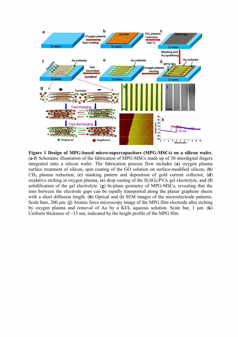
Figure 1 Design of MPG-based micro-supercapacitors (MPG-MSCs) on a silicon wafer.
(a-f) Schematic illustration of the fabrication of MPG-MSCs made up of 30 interdigital fingers
integrated onto a silicon wafer. The fabrication process flow includes (a) oxygen plasma
surface treatment of silicon, spin coating of the GO solution on surface-modified silicon, (b)
CH4 plasma reduction, (c) masking pattern and deposition of gold current collector, (d)
oxidative etching in oxygen plasma, (e) drop casting of the H2SO4/PVA gel electrolyte, and (f)
solidification of the gel electrolyte. (g) In-plane geometry of MPG-MSCs, revealing that the
ions between the electrode gaps can be rapidly transported along the planar graphene sheets
with a short diffusion length. (h) Optical and (i) SEM images of the microelectrode patterns.
Scale bars, 200 m. (j) Atomic force microscopy image of the MPG film electrode after etching
by oxygen plasma and removal of Au by a KI/I2 aqueous solution. Scale bar, 1 m. (k)
Uniform thickness of ~15 nm, indicated by the height profile of the MPG film.

The Key Laboratory of Weak Light Nonlinear Photonics, Ministry of Education, Teda Applied Physics School,
and School of Physics, Nankai University, Tianjin 300457, China
The Key Laboratory of Functional Polymer Materials and Center for Nanoscale Science & Technology,
Institute of Polymer Chemistry, College of Chemistry, Nankai University, Tianjin 300071, China
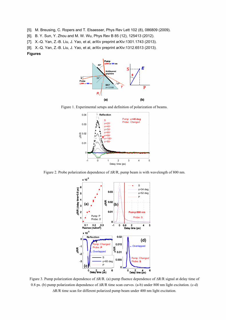
T
R
E
n T
R
E
n
Changed
S
Changed
Changed
S
Changed
Changed
S
Changed
Changed
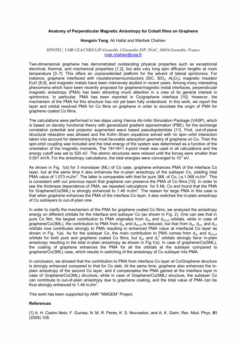
Anatomy of Perpendicular Magnetic Anisotropy for Cobalt films on Graphene
Hongxin Yang, Ali Hallal and Mairbek Chshiev
SPINTEC, UMR CEA/CNRS/UJF-Grenoble 1/Grenoble-INP, INAC, 38054 Grenoble, France
Two-dimensional graphene has demonstrated outstanding physical properties such as exceptional electrical, thermal, and mechanical properties [1,2], but also very long spin diffusion lengths at room temperature [3 7]. This offers an unprecedented platform for the advent of lateral spintronics. For instance, graphene interfaced with insulators/semiconductors (SiC, SiO2, Al2O3), magnetic insulator EuO [8,9], and magnetic metals have been intensively studied in recent years. Among many interesting phenomena which have been recently proposed for graphene/magnetic metal interfaces, perpendicular magnetic anisotropy (PMA) has been attracting much attention in a view of its general interest in spintronics. In particular, PMA has been reported in Co/graphene interface [10]. However, the mechanism of the PMA for this structure has not yet been fully understood. In this work, we report the layer and orbital resolved PMA for Co films on graphene in order to elucidate the origin of PMA for graphene coated Co films. The calculations were performed in two steps using Vienna Ab-Initio Simulation Package (VASP), which is based on density functional theory with generalized gradient approximation (PBE), for the exchange correlation potential and projector augmented wave based pseudopotentials [11]. First, out-of-plane structural relaxation was allowed and the Kohn Sham equations solved with no spin orbit interaction taken into account for determining the most favorable adsorption geometry of graphene on Co. Then the spin-orbit coupling was included and the total energy of the system was determined as a function of the orientation of the magnetic moments. The 19×19×1 k-point mesh was used in all calculations and the energy cutoff was set to 520 eV. The atomic structures were relaxed until the forces were smaller than 0.001 eV/Å. For the anisotropy calculations, the total energies were converged to 10
-7 eV.
As shown in Fig. 1(a) for 3 monolayer (ML) of Co case, graphene enhances PMA of the interface Co layer, but at the same time it also enhances the in-plain anisotropy of the sublayer Co, yielding total PMA value of 1.073 mJ/m
2. The latter is comparable with that for pure 3ML of Co, i.e.1.068 mJ/m
2. This
is consistent with our previous report that graphene can preserve the PMA of Co films [10]. In order to see the thickness dependence of PMA, we repeated calculations for 5 ML Co and found that the PMA for Graphene/Co(5ML) is strongly enhanced to 1.46 mJ/m
2. The reason for large PMA in this case is
that when graphene enhances the PMA of the interface Co layer, it also switches the in-plain anisotropy of Co sublayers to out-of-plain one. In order to clarify the mechanism of the PMA for graphene coated Co films, we analyzed the anisotropy energy on different orbitals for the interface and sublayer Co (as shown in Fig. 2). One can see that in pure Co film, the largest contribution to PMA originates from dxy and dx2-y2 orbitals, while in case of graphene/Co(3ML), the contribution to PMA from dxy and dx2-y2 is reduced, but that from dxz, dyz, and dz2 orbitals now contributes strongly to PMA resulting in enhanced PMA value at interfacial Co layer as shown in Fig. 1(a). As for the sublayer Co, the main contribution to PMA comes from dxy and dx2-y2 orbitals for both pure and graphene coated Co films, but dyz and dz
2 orbitals strongly favor in-plain
anisotropy resulting in the total in-plain anisotropy as shown in Fig.1(a). In case of graphene/Co(5ML), the coating of graphene enhances the PMA for all the orbitals at the sublayer compared to graphene/Co(3ML) case, which results in switching of the anisotropy of Co sublayer into PMA. In conclusion, we showed that the contribution to PMA from interface Co layer at Co/Graphene structure is strongly enhanced compared to that for Co slab. At the same time, graphene also enhances the in-plain anisotropy of the second Co layer, and it compensates the PMA gained at the interface layer in case of Graphene/Co(3ML) structure, while in case of Graphene/Co(5ML) structure, the sublayer Co can contribute to out-of-plain anisotropy due to graphene coating, and the total value of PMA can be thus strongly enhanced to 1.46 mJ/m
2.
References [1] A. H. Castro Neto, F. Guinea, N. M. R. Peres, K. S. Novoselov, and A. K. Geim, Rev. Mod. Phys. 81 (2009) 109.
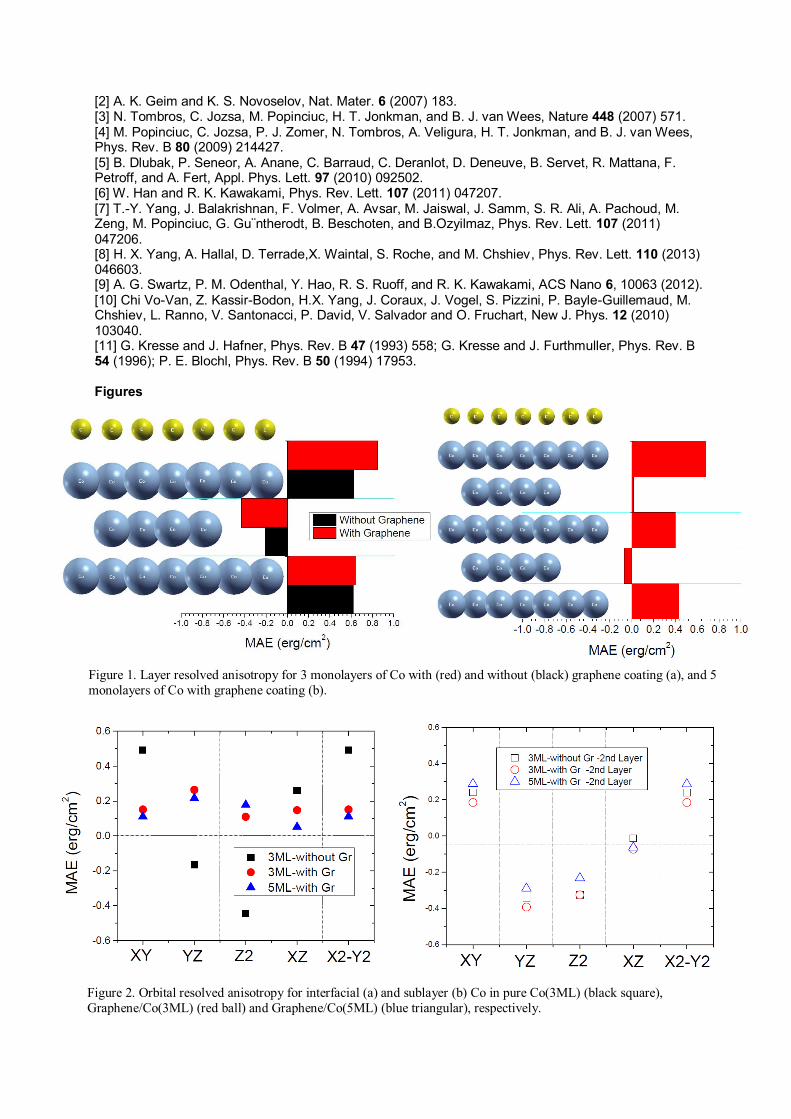
[2] A. K. Geim and K. S. Novoselov, Nat. Mater. 6 (2007) 183. [3] N. Tombros, C. Jozsa, M. Popinciuc, H. T. Jonkman, and B. J. van Wees, Nature 448 (2007) 571. [4] M. Popinciuc, C. Jozsa, P. J. Zomer, N. Tombros, A. Veligura, H. T. Jonkman, and B. J. van Wees, Phys. Rev. B 80 (2009) 214427. [5] B. Dlubak, P. Seneor, A. Anane, C. Barraud, C. Deranlot, D. Deneuve, B. Servet, R. Mattana, F. Petroff, and A. Fert, Appl. Phys. Lett. 97 (2010) 092502. [6] W. Han and R. K. Kawakami, Phys. Rev. Lett. 107 (2011) 047207. [7] T.-Y. Yang, J. Balakrishnan, F. Volmer, A. Avsar, M. Jaiswal, J. Samm, S. R. Ali, A. Pachoud, M. Zeng, M. Popinciuc, G. Gu¨ntherodt, B. Beschoten, and B.Ozyilmaz, Phys. Rev. Lett. 107 (2011) 047206. [8] H. X. Yang, A. Hallal, D. Terrade,X. Waintal, S. Roche, and M. Chshiev, Phys. Rev. Lett. 110 (2013) 046603. [9] A. G. Swartz, P. M. Odenthal, Y. Hao, R. S. Ruoff, and R. K. Kawakami, ACS Nano 6, 10063 (2012). [10] Chi Vo-Van, Z. Kassir-Bodon, H.X. Yang, J. Coraux, J. Vogel, S. Pizzini, P. Bayle-Guillemaud, M. Chshiev, L. Ranno, V. Santonacci, P. David, V. Salvador and O. Fruchart, New J. Phys. 12 (2010) 103040. [11] G. Kresse and J. Hafner, Phys. Rev. B 47 (1993) 558; G. Kresse and J. Furthmuller, Phys. Rev. B 54 (1996); P. E. Blochl, Phys. Rev. B 50 (1994) 17953. Figures
Figure 1. Layer resolved anisotropy for 3 monolayers of Co with (red) and without (black) graphene coating (a), and 5
monolayers of Co with graphene coating (b).
Figure 2. Orbital resolved anisotropy for interfacial (a) and sublayer (b) Co in pure Co(3ML) (black square),
Graphene/Co(3ML) (red ball) and Graphene/Co(5ML) (blue triangular), respectively.
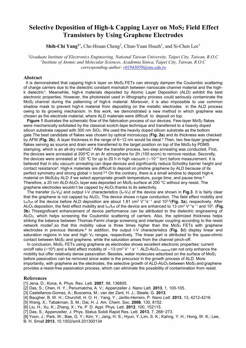
Selective Deposition of High-k Capping Layer on MoS2 Field Effect
Transistors by Using Graphene Electrodes
Shih-Chi Yang1*, Che-Hsuan Cheng2, Chun-Yuan Hsueh1, and Si-Chen Lee1
1Graduate Institute of Electronics Engineering, National Taiwan University, Taipei City, Taiwan, R.O.C 2Institute of Atomic and Molecular Sciences, Academia Sinica, Taipei City, Taiwan, R.O.C
corresponding author: [email protected]
Abstract It is demonstrated that capping high-k layer on MoS2 FETs can strongly dampen the Coulombic scattering of charge carriers due to the dielectric constant mismatch between nanoscale channel material and the high-k dielectric1. Meanwhile, high-k materials deposited by Atomic Layer Deposition (ALD) exhibit the best electronic properties. However, the photoresist used in lithography process could seriously contaminate the MoS2 channel during the patterning of high-k material. Moreover, it is also impossible to use common shadow mask to prevent high-k material from depositing on the metallic electrodes in the ALD process owing to its growing mechanism. In this work, we demonstrated a new method in which graphene was chosen as the electrode material, where ALD materials were difficult to deposit on top. Figure 1 ow of the fabrication process of our devices. Few-layer MoS2 flakes were mechanically exfoliated by the classical scotch-tape technique and transferred to a heavily doped silicon substrate capped with 300 nm SiO2. We used the heavily doped silicon substrate as the bottom gate.The best candidate of flakes was chosen by optical microscopy (Fig. 2a) and its thickness was checked by AFM (Fig. 2b). A layer thickness in the range of 6 12 nm would be ideal.2 Then, two few-layer graphene flakes serving as source and drain were transferred to the target position on top of the MoS2 by PDMS stamping, which is an all-dry method.3 After the transfer process, two-step annealing was conducted. First, the devices were annealed at 200°C in an Ar atmosphere for 2h (100 sccm) to remove residue. Secondly, the devices were annealed at 120 °C for up to 20 h in high vacuum ( 10 7 torr) before measurement. It is believed that in situ vacuum annealing can dope devices and significantly reduce Schottky barrier height and contact resistance4. High-k materials are difficult to deposit on pristine graphene by ALD because of its perfect symmetry and strong global bond.5,6 On the contrary, there is a small window to deposit high-k material on MoS2by ALD if we select appropriate growth temperature, purge time, and pause time.6
Therefore, a 20 nm ALD-Al2O3 layer was deposited on MoS2 surface at 200 °C without any resist. The graphene electrodes be capped by Al2O3 thanks to its selectivity. The transfer (Id-Vg) and output I-V characteristics (Id-Vd) of the device are shown in Fig.3. It is fairly clear that the graphene is not capped by Al2O3. The device shows n-type conduction. TIon/Ioff of the device before ALD deposition are about 1.81 cm2 V 1s 1 and 103.5(Fig. 3a), respectively. After Al2O3 deposition, t on/Ioff of the device are enhanced to 13 cm2 V 1s 1 and 105. (Fig. 3b) Thissignificant enhancement of device performance can be attributed to the dielectric engineering of Al2O3, which helps screening the Coulombic scattering of carriers. Also, the optimized thickness helps striking the balance between Thomas-Fermi charge screening and interlayer coupling according to the resist network model7,so that this mobility value is three times higher than the MoS2 FETs with graphene electrodes in previous literature.8 In addition, the output I-V characteristics (Fig. 3d) display linear and saturation regions in low and high Vd ranges, respectively. The linear part is attributed to the quasi-ohmic contact between MoS2 and graphene, while the saturation arises from the channel pinch-off. In conclusion, MoS2 FETs using graphene as electrodes shows excellent electronic properties: current
on/off ratio (~105) and a 13 cm2 V 1 s 1. ALD-Al2O3 capping can not only enhance the mobility but offer relatively dense passivation. Besides, water molecules adsorbed on the surface of MoS2 before passivation can be removed since water is the precursor in the growth process of ALD. More importantly, with graphene as the electrodes, the selective growth of ALD-Al2O3 between MoS2 and graphene provides a resist-free passivation process, which can eliminate the possibility of contamination from resist.
References [1] Jena, D.; Kona, A. Phys. Rev. Lett. 2007, 98, 136805. [2] Das, S.; Chen, H. Y.; Penumatcha, A. V.; Appenzeller J. Nano Lett. 2013, 1, 100-105. [3] Castellanos-Gomez, A.; Buscema, M.; van der Zant, H. J.; Steele, G. 2013. [4] Baugher, B. W. H.; Churchill, H. O. H.; Yang, Y.; Jarillo-Herrero, P. Nano Lett. 2013, 13, 4212-4216. [5] Wang, X.; Tabakman, S. M.; Dai, H. J. Am. Chem. Soc. 2008, 130, 8152. [6] Liu, H.; Xu, K.; Zhang, X.; Ye, P. D. Appl. Phys. Lett. 2012, 100, 152115. [7] Das, S.; Appenzeller, J. Phys. Status Solidi Rapid Res. Lett. 2013, 7, 268 273. [8] Yoon, J.; Park, W.; Bae, G. Y.; Kim, Y.; Jang, H. S.; Hyun, Y.;Lim, S. K.; Kahng, Y. H.; Hong, W. K.; Lee, B. H. Small 2013, 10.1002/smll.201300134
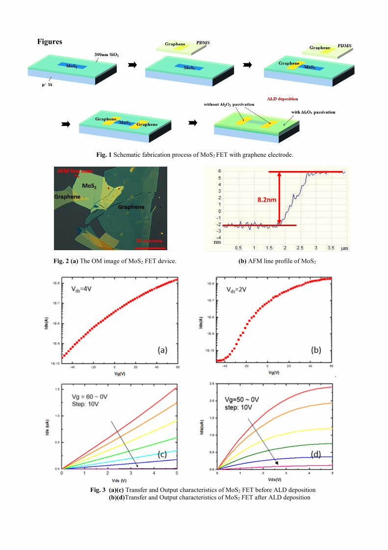
Figures
Fig. 1 Schematic fabrication process of MoS2 FET with graphene electrode.
Fig. 2 (a) The OM image of MoS2 FET device. (b) AFM line profile of MoS2
Fig. 3 (a)(c) Transfer and Output characteristics of MoS2 FET before ALD deposition
(b)(d)Transfer and Output characteristics of MoS2 FET after ALD deposition
8.2nm
m
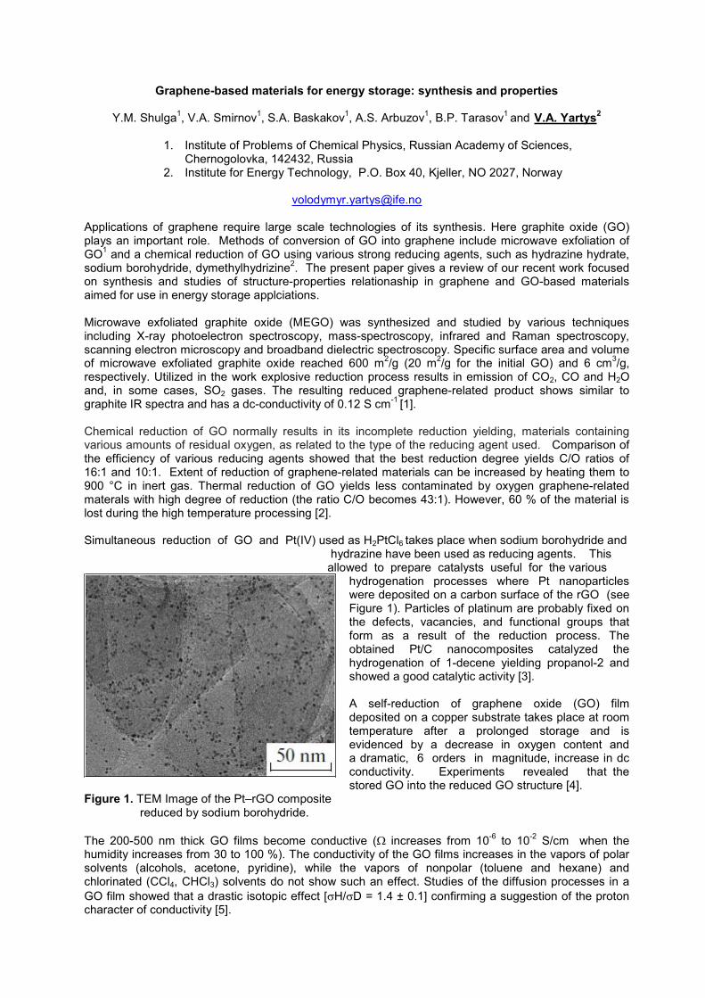
Graphene-based materials for energy storage: synthesis and properties
Y.M. Shulga1, V.A. Smirnov
1, S.A. Baskakov
1, A.S. Arbuzov
1, B.P. Tarasov
1and V.A. Yartys
2
1. Institute of Problems of Chemical Physics, Russian Academy of Sciences, Chernogolovka, 142432, Russia
2. Institute for Energy Technology, P.O. Box 40, Kjeller, NO 2027, Norway
Applications of graphene require large scale technologies of its synthesis. Here graphite oxide (GO)plays an important role. Methods of conversion of GO into graphene include microwave exfoliation of GO
1and a chemical reduction of GO using various strong reducing agents, such as hydrazine hydrate,
sodium borohydride, dymethylhydrizine2. The present paper gives a review of our recent work focused
on synthesis and studies of structure-properties relationaship in graphene and GO-based materials aimed for use in energy storage applciations.
Microwave exfoliated graphite oxide (MEGO) was synthesized and studied by various techniques including X-ray photoelectron spectroscopy, mass-spectroscopy, infrared and Raman spectroscopy, scanning electron microscopy and broadband dielectric spectroscopy. Specific surface area and volume of microwave exfoliated graphite oxide reached 600 m
2/g (20 m
2/g for the initial GO) and 6 cm
3/g,
respectively. Utilized in the work explosive reduction process results in emission of CO2, CO and H2Oand, in some cases, SO2 gases. The resulting reduced graphene-related product shows similar to graphite IR spectra and has a dc-conductivity of 0.12 S cm
-1[1].
Chemical reduction of GO normally results in its incomplete reduction yielding, materials containingvarious amounts of residual oxygen, as related to the type of the reducing agent used. Comparison of the efficiency of various reducing agents showed that the best reduction degree yields C/O ratios of 16:1 and 10:1. Extent of reduction of graphene-related materials can be increased by heating them to 900 °C in inert gas. Thermal reduction of GO yields less contaminated by oxygen graphene-related materals with high degree of reduction (the ratio C/O becomes 43:1). However, 60 % of the material is lost during the high temperature processing [2].
Simultaneous reduction of GO and Pt(IV) used as H2PtCl6 takes place when sodium borohydride and hydrazine have been used as reducing agents. This allowed to prepare catalysts useful for the various
hydrogenation processes where Pt nanoparticles were deposited on a carbon surface of the rGO (see Figure 1). Particles of platinum are probably fixed on the defects, vacancies, and functional groups that form as a result of the reduction process. The obtained Pt/C nanocomposites catalyzed the hydrogenation of 1-decene yielding propanol-2 and showed a good catalytic activity [3].
A self-reduction of graphene oxide (GO) film deposited on a copper substrate takes place at room temperature after a prolonged storage and is evidenced by a decrease in oxygen content and a dramatic, 6 orders in magnitude, increase in dc conductivity. Experiments revealed that the stored GO into the reduced GO structure [4].
Figure 1. TEM Image of the Pt–rGO composite reduced by sodium borohydride.
The 200-500 nm thick GO films become conductive ( increases from 10-6
to 10-2
S/cm when the humidity increases from 30 to 100 %). The conductivity of the GO films increases in the vapors of polar solvents (alcohols, acetone, pyridine), while the vapors of nonpolar (toluene and hexane) and chlorinated (CCl4, CHCl3) solvents do not show such an effect. Studies of the diffusion processes in a
GO film showed that a drastic isotopic effect [ H/ D = 1.4 ± 0.1] confirming a suggestion of the proton character of conductivity [5].
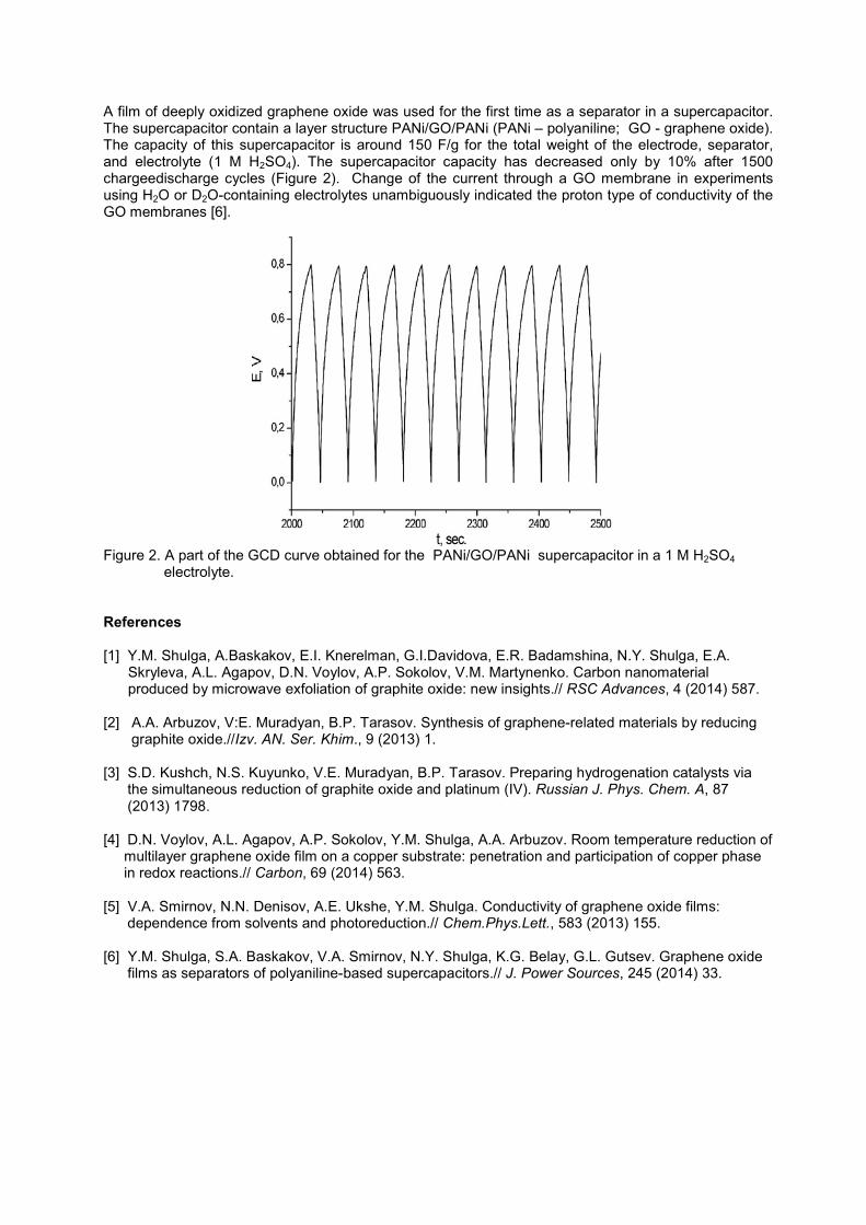
A film of deeply oxidized graphene oxide was used for the first time as a separator in a supercapacitor. The supercapacitor contain a layer structure PANi/GO/PANi (PANi – polyaniline; GO - graphene oxide).The capacity of this supercapacitor is around 150 F/g for the total weight of the electrode, separator, and electrolyte (1 M H2SO4). The supercapacitor capacity has decreased only by 10% after 1500 chargeedischarge cycles (Figure 2). Change of the current through a GO membrane in experiments using H2O or D2O-containing electrolytes unambiguously indicated the proton type of conductivity of the GO membranes [6].
Figure 2. A part of the GCD curve obtained for the PANi/GO/PANi supercapacitor in a 1 M H2SO4
electrolyte.
References
[1] Y.M. Shulga, A.Baskakov, E.I. Knerelman, G.I.Davidova, E.R. Badamshina, N.Y. Shulga, E.A.Skryleva, A.L. Agapov, D.N. Voylov, A.P. Sokolov, V.M. Martynenko. Carbon nanomaterial produced by microwave exfoliation of graphite oxide: new insights.// RSC Advances, 4 (2014) 587.
[2] A.A. Arbuzov, V:E. Muradyan, B.P. Tarasov. Synthesis of graphene-related materials by reducing graphite oxide.//Izv. AN. Ser. Khim., 9 (2013) 1.
[3] S.D. Kushch, N.S. Kuyunko, V.E. Muradyan, B.P. Tarasov. Preparing hydrogenation catalysts via the simultaneous reduction of graphite oxide and platinum (IV). Russian J. Phys. Chem. A, 87 (2013) 1798.
[4] D.N. Voylov, A.L. Agapov, A.P. Sokolov, Y.M. Shulga, A.A. Arbuzov. Room temperature reduction ofmultilayer graphene oxide film on a copper substrate: penetration and participation of copper phase in redox reactions.// Carbon, 69 (2014) 563.
[5] V.A. Smirnov, N.N. Denisov, A.E. Ukshe, Y.M. Shulga. Conductivity of graphene oxide films: dependence from solvents and photoreduction.// Chem.Phys.Lett., 583 (2013) 155.
[6] Y.M. Shulga, S.A. Baskakov, V.A. Smirnov, N.Y. Shulga, K.G. Belay, G.L. Gutsev. Graphene oxide films as separators of polyaniline-based supercapacitors.// J. Power Sources, 245 (2014) 33.
Effect of Reduced Graphene Oxide Cap Layer on Electromigration Reliability of Cu Interconnect
Seong Jun Yoon, Sung-Yool Choi, and Byung Jin Cho
Department of Electrical Engineering, KAIST, 291 Daehak-Ro, Yuseong-gu, Daejeon 305-701, [email protected]
As the interconnect size have been scaled down, electromigration (EM) becomes one of the major
issues of Cu interconnect reliability. In the typical Cu damascene structure, the location of Cu and
Si(C)N dielectric layer interface is the weakest point of electromigration-induced failure. Therefore,
introducing metallic cap layer, such as tungsten [1] or CoWP [2], could effectively increase the EM
lifetime of Cu interconnect. However, difficulty in process optimization and cost efficiency become major
barriers [3]. Moreover, as the Cu line width reduces, ultra-thin cap layer with high EM blocking ability is
necessary. Graphene-based 2-D materials, which have atomically thin nature, could have strong
potential to application of Cu interconnect cap layer. In this work, we investigate that a reduced
graphene oxide (rGO) cap layer effectively blocks the migration path of Cu surface, and therefore, the
EM lifetime of Cu line is improved. The rGO cap layer was fabricated by dip-coating of water-dispersible
graphene oxide solution and subsequent reduction with hydrogen ambient annealing. The
electromigration test was conducted under highly accelerated wafer level test and the mean
temperature of the Cu line was estimated [4]. The EM test results indicate the major diffusion
mechanism of Cu atom is changed from surface diffusion to grain boundary diffusion, because of the
EM blocking by rGO cap layer. The Observation of Cu line morphology by scanning electron microscopy
also support the result of increased EM lifetime by rGO cap. A possible mechanism for reduced surface
diffusivity of Cu line is also proposed.

References
[1] T. Saito et al., IEEE Trans. Electron Devices, 51 (2004), 2129.[2] C.-K. Hu et al., Microelectron. Eng., 70 (2003), 406.[3] C.-C. Yang et al., IEEE Electron Device Lett., 31 (2010), 728.[4] A. Zitzelsberger et al., Proc. Int. Reliability Physics Symp., (2003), 161.
Figures
Figure 1. Fabrication process of rGO cap layer on Cu line
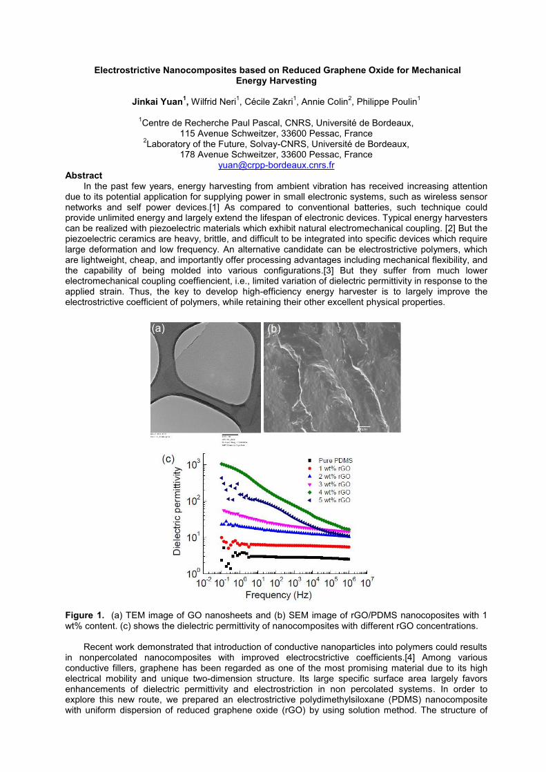
Electrostrictive Nanocomposites based on Reduced Graphene Oxide for Mechanical Energy Harvesting
Jinkai Yuan
1, Wilfrid Neri
1, Cécile Zakri
1, Annie Colin
2, Philippe Poulin
1
1Centre de Recherche Paul Pascal, CNRS, Université de Bordeaux,
115 Avenue Schweitzer, 33600 Pessac, France 2Laboratory of the Future, Solvay-CNRS, Université de Bordeaux,
178 Avenue Schweitzer, 33600 Pessac, France [email protected]
Abstract In the past few years, energy harvesting from ambient vibration has received increasing attention
due to its potential application for supplying power in small electronic systems, such as wireless sensor networks and self power devices.[1] As compared to conventional batteries, such technique could provide unlimited energy and largely extend the lifespan of electronic devices. Typical energy harvesters can be realized with piezoelectric materials which exhibit natural electromechanical coupling. [2] But the piezoelectric ceramics are heavy, brittle, and difficult to be integrated into specific devices which require large deformation and low frequency. An alternative candidate can be electrostrictive polymers, which are lightweight, cheap, and importantly offer processing advantages including mechanical flexibility, and the capability of being molded into various configurations.[3] But they suffer from much lower electromechanical coupling coeffiencient, i.e., limited variation of dielectric permittivity in response to the applied strain. Thus, the key to develop high-efficiency energy harvester is to largely improve the electrostrictive coefficient of polymers, while retaining their other excellent physical properties.
Figure 1. (a) TEM image of GO nanosheets and (b) SEM image of rGO/PDMS nanocoposites with 1 wt% content. (c) shows the dielectric permittivity of nanocomposites with different rGO concentrations.
Recent work demonstrated that introduction of conductive nanoparticles into polymers could results
in nonpercolated nanocomposites with improved electrocstrictive coefficients.[4] Among various conductive fillers, graphene has been regarded as one of the most promising material due to its high electrical mobility and unique two-dimension structure. Its large specific surface area largely favors enhancements of dielectric permittivity and electrostriction in non percolated systems. In order to explore this new route, we prepared an electrostrictive polydimethylsiloxane (PDMS) nanocomposite with uniform dispersion of reduced graphene oxide (rGO) by using solution method. The structure of

nanosheet inclusion was carefully characterized by spectroscopy methods (Figure 1a). The uniform dispersion state of rGO in final PDMS composites was confirmed by scanning electron microscopy (Figure 1b). The reduction of GO in PDMS matrix can be thermally induced to increase the conductivity contrast between filler and matrix, which is favorable for increasing the dielectric permittivity of PDMS composites (Figure 1c). First characterizations of dielectric properties confirm the possibility to achieve enhancements of dielectric permittivity and electrostriction in this novel graphene based nanocomposites. References [1] S. Priya, J. Electroceram., 19 (2007) 167. [2] D. Guyomar, A. Badel, et al. IEEE Trans. Ultrason. Ferroelectr. Freq. Control., 52 (2005) 584. [3] Q. M. Zhang, V. Bharti, X. Zhao, Science, 280 (1998) 2101. [4] C. Putson, L. Lebrun, D. Guyomar, N. Muensit, et al. J. Appl. Phys. 109 (2011) 024104.

Graphene-multiferroic heterostructures: electronic and magnetic properties by design
Zeila Zanolli
Forschungszentrum Jülich, PGI-1 & IAS-1, Wilhelm-Johnen-Strasse 52425, Jülich, [email protected]
Abstract
Spintronics is the new paradigm of information technology. The operating principle of the spin transistor [1] relies on the modulation of the current thanks to the Spin-Orbit (SO) Coupling in semiconducting materials and on spin injection via magnetized contacts. However the devices fabricated with conventional semiconductors suffer from short spin diffusion lengths and result in weak spin signals. C-based nanomaterials, instead, are considered highly promising for spintronic applications since can present spin diffusion lengths up to the 100 µm range and high electron velocity. However, a large spin diffusion length comes at the price of small SO coupling, which limits the possibility of manipulating electrons via an external applied field. In addition, to achieve graphene-based devices one also needs to open its vanishing electronic gap.
One way to open a band gap in graphene and preserve high carrier mobility is to put graphene on a suitable substrate. If, in addition, the substrate is insulating and magnetic, magnetism can be induced in the graphene sheet by proximity interaction [2, 3, 4]. Based on these considerations, we have investigated from first-principles an heterostructure consisting of the magnetoelectric (ferroelectric and magnetic) insulating BaMnO3 [5] sandwiched between two graphene sheets [Fig. 1]. The ground state of BaMnO3 is hexagonal and fits on the 4x4 graphene cell. The calculations have been performed using the SIESTA code in the local spin density (LDA) approximation, using a basis set and computational parameters optimized for the accurate modeling of ferroelectricity and magnetism in bulk BaMnO3. In this framework we predict that the Mn atoms present an A-type antiferromagnetic order with spins antiparallel along the heterostructure direction and parallel in each layer. Magnetism is induced in the
graphene sheets thanks to the high magnetic moment residing on the Mn atoms (~ 2.4 µB) and to the strong interaction between graphene and the Mn-terminated side of the slab. The spin density of the heterostructure, illustrated in Fig. 2, shows that the strongest magnetization is induced on the C atoms belonging to hexagons centered on the Mn atoms. Majority (black lines in Fig. 3) and minority (red lines in Fig. 3) carriers are characterized by quite different electronic properties: The band-gap for majority
and minority carriers occurs, respectively, on the M-Γ line and at the K point, predicting an anisotropy between the two types of carrier. The electronic gap is inherited from the BaMnO3. The graphene Dirac cones are into the valence band with a slope dependent on the spin type, hence producing a spin-depended carrier mobility in the whole heterostructure.
Z.Z. acknowledges EC support under the Marie-Curie fellowship (PIEF-Ga-2011-300036). The results of this research have been achieved using the PRACE-3IP project (FP7 RI-312763) resource "Lindgren"based in Sweden at KTH. Computing resources granted by JARA-HPC from RWTH Aachen University under project "jara0088" were also used.
References
[1] S. Datta and B. Das, Appl. Phys. Lett. 56 (1990) 665.[2] M. Weser et al., Appl. Phys. Lett. 96 (2010) 012504[3] H. Haugen, D. Huertas-Hernando, A. Brataas, Phys. Rev. B, 77, 115406 (2008) [4] H. X. Yang A. Hallal, D. Terrade, X. Waintal, S. Roche, and M. Chshiev Phys. Rev. Lett. 110 (2013) 046603.[5] J. Varignon and Ph. Ghosez, Phys. Rev. B 87, (2013) 140403(R)[6] J. M. Soler, E. Artacho, J. D. Gale, A. Garcia, J. Junquera, P. Ordejon and D. Sanchez-Portal, J. Phys. Condens. Matter 14, 2745 (2002)

Figures
Figure 1. Ball-and-stick model of the heterostructure consisting of 13 monolayers of BaMnO3 sandwiched between two graphene sheets. The color code is: Ba = green, Mn = yellow, O = red, C = gold.
Figure 2. Spin density (ρ↑ - ρ↓) of the hybrid graphene-BaMnO3 system. Red and blue isosurfaces indicate majority
and minority spin densities. The greatest spin polarization is induced on the C atoms belonging to the hexagonscentered on Mn atoms.
Figure 3 Spin-polarized electronic band structure of the graphene-BaMnO3 sandwich structure. Majority and minority spin channels are indicated with black and red lines. The graphene bands are duplicated due to the presence of two graphene sheets in the heterostructure. The Fermi level is used as a reference for the energy.

Stresses Induced Piezoelectric Response in Monolayer Graphene
P. S. Zelenovskiy1, G. R. Cunha
2, M. K. Singh
3, A. L. Kholkin
1,2, V. Ya. Shur
1
1 Ural Federal University, Nanofer laboratory, 620000, 51 Lenin Ave., Ekaterinburg, Russia
2 University of Aveiro, DEMaC & CICECO, 3810-193 Aveiro, Portugal
3 University of Aveiro, Dept. of Mechanical Engng & TEMA, 3810-193 Aveiro, Portugal
A piezoelectric response of monolayer graphene (MLG) deposited on silicon SPM calibration grating has been revealed by Piezoresponse Force Microscopy (PFM). A strong correlation between the topography and piezoelectric response was found (Figure 1). Piezoresponse value on the grating depressions (suspended graphene) appeared close to 0, whereas essentially negative values were observed on the ridges. The observed piezoresponse can be attributed to stresses appeared at the grating ridges. Raman spectroscopy was used for estimation of the stress spatial distribution in MLG.
Raman spectroscopy is a widely used technique for examination of various properties of the graphene [1]: the number and orientation of layers, the quality and types of the edges, the effects of perturbations, such as electric and magnetic fields, strain, doping, disorder and functional groups etc. The typical Raman spectrum of monolayer graphene (MLG) consists of 3 main lines: D, G and 2D bands. The D-band (at about 1350 cm
-1) is due to the breathing vibrations of sp
2 carbon rings and
requires defects for its activation in the spectrum. The doubly degenerated G-band (at about 1580 cm-1
) corresponds to in-plane vibration of sp
2 carbon atoms and is ideal for studies of in-plane stress and
strain in different graphitic. The 2D-band (at about 2672 cm-1
) is a second order of the D-band. This is a single peak in MLG and splits into 4 peaks in bilayer graphene [1-3].
Raman spectroscopy was applied for the examination of tensile and compressive stresses existed in monolayer graphene deposited on a silicon SPM calibration grating. Variations of G-band position in Raman spectrum allowed estimating the stress values from -78 GPa up to +78 GPa. Positive sign corresponds to the tension of the graphene sheet, whereas the negative one to the compression. Tensile stresses periodically occurred at the ridges of the silicon grating, while the compressive stresses were mainly localized around graphene holes and wrinkles.
The studied MLG were grown via CVD technique on copper substrates, and then were transferred onto the Si/SiO2 grating substrate by a wet process. The grating consists of periodical
stripes with a height of about 1.3 m and a period of 3 m. Confocal Raman microscope Alpha 300AR (WiTec GmbH, Germany) was used for mapping of
MLG. Periodic changes of the integrated intensity, position and full width at half-maximum of both G and 2D-bands has been revealed. The period of these changes coincides with the period of Si grating
(3 m). The G-band position increased at grating ridges and decreases at depressions. The maximum range of these variations was about 1.4 cm
-1.
Observed shift of G-band allowed estimating the stresses in MLG [4]. Spatial distribution of the stresses (stress map) is shown in Figure 2a. Stress values vary in wide range from -78 GPa up to +78 GPa. Positive sign here corresponds to the tension of the graphene sheet, whereas the negative one shows the compression. Tensile stresses periodically were occurred at the ridges of the silicon grating, while the compressive stresses were mainly localized around graphene holes and wrinkles (Figure 2b).
Sciences, Ural Federal University has been used. The work was supported by the Portuguese Foundation for Science and Technology (FCT) via grant PTDC/CTM-NAN/121313/2010 and by WiTec GmbH via the travel grant.
References: [1] A.C. Ferrari and D.M. Basko, Nat. Nanotechnol., 8 (2013) 235. [2] Y. ying Wang, Z. hua Ni, T. Yu, Z.X. Shen, et al., J. Phys. Chem. C, 112 (2008) 10637. [3] J.-U. Lee, D. Yoon, and H. Cheong, Nano Lett. 12 (2012) 4444. [4] O. Frank et al., Nat. Commun., 2 (2011) 255.

Figures:
Figure 1. Superposition of cross-sections of topography and piezoresponse signal.
(a) Figure 2. (a) Stress map of SLG on the silicon grating and (b) variations of stress across the grating (blue line). Shaded rectangles correspond to grating ridges.
1
Graphene: A Platform for Surface Enhanced Raman Spectroscopy
Jin Zhang Peking University
China
Surface enhanced Raman scattering (SERS) imparts Raman spectroscopy the capability of detecting
analytes at the single molecule level, but the cost is also manifold, such as loss on signal
reproducibility. Despite remarkable steps have been taken forward, presently SERS still seems too
young to shoulder the analytical missions in various practical situations. By the virtue of its unique
molecular structure and physical/chemical properties, the rise of graphene opens up a unique platform
for SERS study. In this talk, the multi-role of graphene played in SERS is overviewed in turn, including
a Raman probe, a substrate, an additive and a building block of a flat surface for SERS. Apart from
versatile improvements on the SERS performance towards applications, graphene-involved SERS
studies are also expected to shed light on the fundamental mechanism of SERS effect.
References:
1. WG Xu, JQ Xiao, YF Chen, YB Chen, X Ling, J Zhang, Graphene veiled gold substrate for surface enhanced Raman spectroscopy, Adv. Mater. 25(6) (2013), 928-932.
2. WG Xu, X Ling, JQ Xiao, MS Dresselhaus, J Kong, H Xu, ZF Liu, J Zhang, Surface enhanced Raman spectroscopy on a flat graphene surface, Proc. Natl. Acad. Sci. U.S.A. 109(24)(2012), 9281-9286.
3. H Xu, LM Xie, HL Zhang, J Zhang, Effect of graphene fermi level on the Raman scattering intensity of molecules on graphene, ACS Nano 5(7)(2011), 5338-5344.
4. X Ling, LM Xie, Y Fang, H Xu, HL Zhang, J Kong, MS Dresselhaus, J Zhang, ZF Liu, Can graphene be used as a substrate for Raman enhancement?, Nano Lett. 10(2)(2010), 553-561.
5. LM Xie, X Ling, Y Fang, J Zhang, ZF Liu, Graphene as a substrate to suppress fluorescence in resonance Raman spectroscopy, J. Am. Chem. Soc. 131(29) (2009), 9890-9891.

Growth and atomic-scale characterization of graphene and graphene-h-BN hybrid on metal
substrates
Yanfeng Zhang, Mengxi Liu, Yabo Gao, Zhongfan Liu
Department of Materials Science and Engineering, College of Engineering; Center for Nanochemistry (CNC), Peking University, Beijing, China
Abstract Under different growth conditions and over different metal substrates of single and polycrystalline, the
thickness, stacking geometry and growth mechanism of graphene should be much different.[1-3]
Scanning tunneling microscope (STM) may be the only in-situ technique for showing the disparity at an
atomic scale. However, the STM characterization of traditional chemical vapor deposition (CVD)
graphene sample is usually limited by the corrugated nature of the substrate (like Cu foils). We have
performed systematic STM studies of the growth and the microscopic structure of graphene on Cu, Pt,
Rh etc. foil substrates, and clarified their growth mechanisms along with the aid of traditional methods
like Raman spectroscopy, scanning electron microscopy (SEM) and so on.[4] Interestingly, we found
that randomly stacked bilayer or few layer segregated graphene on Rh foils usually exhibit various moiré
patterns, on which angel-dependent van hove singularities was observed by STM/STS.[5,6] Moreover,
we showed that h-BN, a structural analogue of graphene, can be patched onto graphene to form a
monolayer hybrid on Rh(111). This hybrid formation was considered be promising for opening up a
small band gap of graphene, and most of the efforts were performed by growing the sample on Cu foil
substrates. In our work, we show that with the deliberately selected Rh(111) substrate, graphene and h-
BN, as well as the interface of hybrid can be recognized by atomic scale STM images. [7] A preferred
zigzag type interface between graphene and h-BN was identified by STM, as also verified by DFT
calculations.
References
[1] Y. F. Zhang, T. Gao, Y. B. Gao, S. B. Xie, Q. Q. Ji, K. Yan, H. L. Peng and Z.F. Liu*, ACS Nano, 5,
(2011) 4014.
[2] T. Gao, S.B. Xie, Y.B. Gao, M.X. Liu, Y.B. Chen, Y.F. Zhang* and Z.F. Liu*, ACS Nano, 5(2011) 9194.
[4] M.X. Liu, Y.B. Gao, Y. F. Zhang*, Y. Zhang, D.L. Ma, Q.Q. Ji, T. Gao, Y.B. Chen, and Z.F. Liu*, Small
9(2013)1360.
[5] M.X. Liu, Y.F. Zhang*, Y.B. Chen, Y.B. Gao, T. Gao, D.L. Ma, Q.Q. Ji, Y. Zhang, C. Li, and Z.F. Liu*,
ACS Nano 6(2012)10581.
[6] W. Yan, M. X. Liu, R. F. Dou, L. Meng, L. Feng, Z. D. Chu, Y. F. Zhang*, Z. F. Liu, J. C. Nie, L. He*,
Phys. Rev. Lett., 109(2012)126801.
[7] W. Yan, W. Y. He, Z. D. Chu, M. X. Liu, L. Meng, R. F. Dou, Y. F. Zhang, Z. F. Liu, J. C. Nie, L. He,
Nat. Commun. 4(2013)2159.
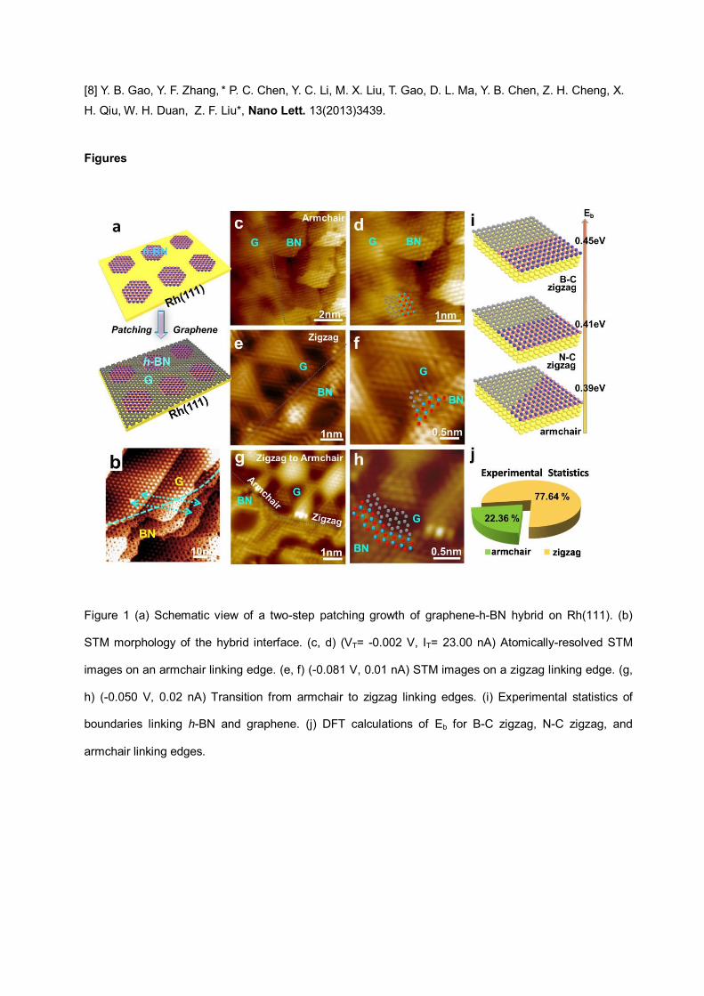
[8] Y. B. Gao, Y. F. Zhang, * P. C. Chen, Y. C. Li, M. X. Liu, T. Gao, D. L. Ma, Y. B. Chen, Z. H. Cheng, X.
H. Qiu, W. H. Duan, Z. F. Liu*, Nano Lett. 13(2013)3439.
Figures
Figure 1 (a) Schematic view of a two-step patching growth of graphene-h-BN hybrid on Rh(111). (b)
STM morphology of the hybrid interface. (c, d) (VT= -0.002 V, IT= 23.00 nA) Atomically-resolved STM
images on an armchair linking edge. (e, f) (-0.081 V, 0.01 nA) STM images on a zigzag linking edge. (g,
h) (-0.050 V, 0.02 nA) Transition from armchair to zigzag linking edges. (i) Experimental statistics of
boundaries linking h-BN and graphene. (j) DFT calculations of Eb for B-C zigzag, N-C zigzag, and
armchair linking edges.


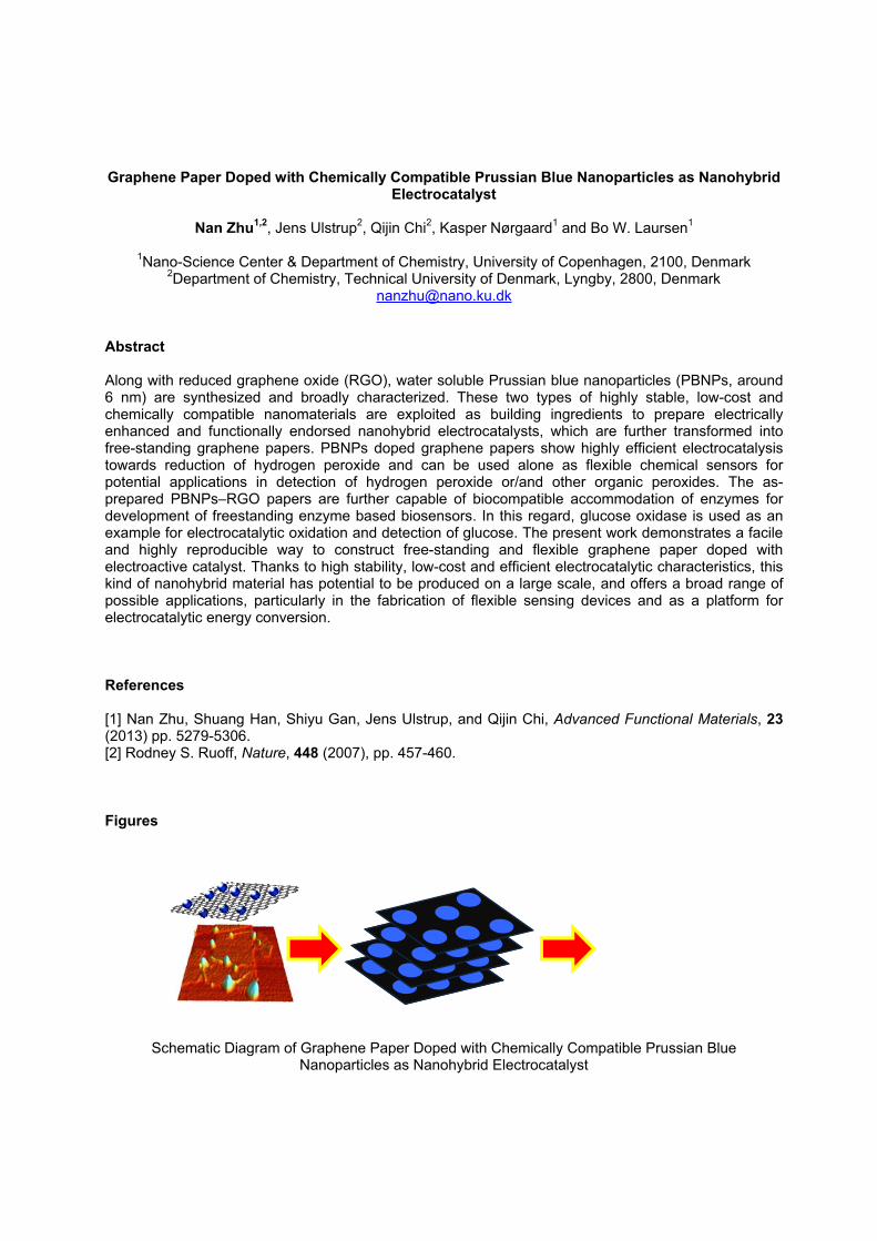
Graphene Paper Doped with Chemically Compatible Prussian Blue Nanoparticles as Nanohybrid Electrocatalyst
Nan Zhu1,2
, Jens Ulstrup2, Qijin Chi
2, Kasper Nørgaard
1 and Bo W. Laursen
1
1Nano-Science Center & Department of Chemistry, University of Copenhagen, 2100, Denmark
2Department of Chemistry, Technical University of Denmark, Lyngby, 2800, Denmark
Abstract
Along with reduced graphene oxide (RGO), water soluble Prussian blue nanoparticles (PBNPs, around 6 nm) are synthesized and broadly characterized. These two types of highly stable, low-cost and chemically compatible nanomaterials are exploited as building ingredients to prepare electrically enhanced and functionally endorsed nanohybrid electrocatalysts, which are further transformed into free-standing graphene papers. PBNPs doped graphene papers show highly efficient electrocatalysis towards reduction of hydrogen peroxide and can be used alone as flexible chemical sensors for potential applications in detection of hydrogen peroxide or/and other organic peroxides. The as-prepared PBNPs–RGO papers are further capable of biocompatible accommodation of enzymes for development of freestanding enzyme based biosensors. In this regard, glucose oxidase is used as an example for electrocatalytic oxidation and detection of glucose. The present work demonstrates a facile and highly reproducible way to construct free-standing and flexible graphene paper doped with electroactive catalyst. Thanks to high stability, low-cost and efficient electrocatalytic characteristics, this kind of nanohybrid material has potential to be produced on a large scale, and offers a broad range of possible applications, particularly in the fabrication of flexible sensing devices and as a platform for electrocatalytic energy conversion.
References
[1] Nan Zhu, Shuang Han, Shiyu Gan, Jens Ulstrup, and Qijin Chi, Advanced Functional Materials, 23(2013) pp. 5279-5306. [2] Rodney S. Ruoff, Nature, 448 (2007), pp. 457-460.
Figures
Schematic Diagram of Graphene Paper Doped with Chemically Compatible Prussian Blue Nanoparticles as Nanohybrid Electrocatalyst
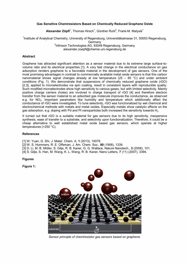
Gas Sensitive Chemiresistors Based on Chemically Reduced Graphene Oxide
Alexander Zöpfl1, Thomas Hirsch
1, Günther Ruhl
2, Frank-M. Matysik
1
1Institute of Analytical Chemistry, University of Regensburg, Universitätsstrasse 31, 93053 Regensburg,
Germany 2Infineon Technologies AG, 93049 Regensburg, Germany
Abstract Graphene has attracted significant attention as a sensor material due to its extreme large surface-to-volume ratio and its electrical properties [1]. A very fast change in the electrical conductance on gas adsorption renders graphene to a favorable material in the development of gas sensors. One of the most promising advantages in contrast to commercially available metal oxide sensors is that this carbon nanomaterial shows signal changes already at low temperature (25 85 °C) and under ambient conditions (Fig. 1). We demonstrate that suspensions of chemically reduced graphene oxide (rGO) [2,3], applied to microelectrodes via spin coating, result in consistent layers with reproducible quality. Such modified microelectrodes show high sensitivity to various gases, but with limited selectivity. Mainly positive charge carriers (holes) are involved in charge transport of rGO [4] and therefore electron transfer from the sensor material to an adsorbed gas molecule improves the conductance, as observed e.g. for NO2. Important parameters like humidity and temperature which additionally affect the conductance of rGO were investigated. To tune selectivity, rGO was functionalized by wet chemical and electrochemical methods with metals and metal oxides. Especially metals show catalytic effects on the gas adsorption, e.g. doping with Pd and Pt nanoparticles both increased the sensitivity towards H2.
It turned out that rGO is a suitable material for gas sensors due to its high sensitivity, inexpensive synthesis, ease of transfer to a substrate, and selectivity upon functionalization. Therefore, it could be a cheap alternative to well established metal oxide based gas sensors, which operate at higher temperatures (>250 °C). References [1] W. Yuan, G. Shi, J. Mater. Chem. A, 1 (2013), 10078. [2] W. S. Hummers, R. E. Offeman, J. Am. Chem. Soc., 80 (1958), 1339. [3] D. Li, M. B. Müller, S. Gilje, R. B. Kaner, G. G. Wallace, Nature Nanotech., 3 (2008), 101. [4] S. Gilje, S. Han, M. Wang, K. L. Wang, R. B. Kaner, Nano Letters, 7 (11) (2007), 3394. Figures Figure 1:
Sensor principle of chemiresistor gas sensors based on graphene.