group iii-arsenide-nitride long wavelength laser diodes
TRANSCRIPT
GROUP III-ARSENIDE-NITRIDE LONG
WAVELENGTH LASER DIODES
A DISSERTATION SUBMITTED TO THE DEPARTMENT OF ELECTRICAL
ENGINEERING AND THE COMMITTEE OF GRADUATE STUDIES OF
STANFORD UNIVERSITY IN PARTIAL FULFILLMENT OF THE
REQUIREMENTS FOR THE DEGREE OF DOCTOR OF PHILOSOPY
By
Christopher W. Coldren
September 2005

©Copyright 2005 by Christopher W. Coldren
All Rights Reserved
ii

I certify that I have read this dissertation and that in my
opinion and is fully adequate, in scope and quality, as a
dissertation for the degree of Doctor of Philosophy.
____________________________________
Prof. James S. Harris
(Principal Advisor)
I certify that I have read this dissertation and that in my
opinion and is fully adequate, in scope and quality, as a
dissertation for the degree of Doctor of Philosophy.
____________________________________
Prof. D. A. B. Miller
I certify that I have read this dissertation and that in my
opinion and is fully adequate, in scope and quality, as a
dissertation for the degree of Doctor of Philosophy.
____________________________________
Dr. M. C. Larson
Approved for the University Committee on Graduate
Studies:
____________________________________
iii
Abstract Semiconductor laser diodes transmitting data over silica optical fiber form the
backbone of modern day communications systems, enabling terabit per second data
transmission over hundreds to thousands of kilometers of distance. The wavelength of
emission of the transmission semiconductor laser diode is a critical parameter that
determines the performance of the communications system. In high performance fiber
optic communications systems, lasers emitting at 1300nm and 1550nm are used because
of the low loss and distortion properties of the fiber in these spectral windows. The
available lasers today that operate in these fiber optic transmission windows suffer from
high cost and poor performance under the typical environmental conditions and require
costly and unreliable cooling systems.
This dissertation presents work that demonstrates that it is possible to make lasers
devices with 1300nm laser emission that are compatible with low cost and operation
under extreme operating conditions. The key enabling technology developed is a novel
semiconductor material based structure. A group III-Arsenide-Nitride quantum well
structure was developed that can be grown expitaxially on GaAs substrates. The
properties of this group III-Arsenide-Nitride structure allowed high performance edge
emitting and vertical cavity surface emitting lasers to be fabricated which exhibited low
threshold currents and low sensitivity to operating temperature.
iv

Acknowledgements
I would like to thank all of the students and faculty that I have had the pleasure of
learning from and working with during my stay at Stanford. In particular, I would like to
thank Professor Harris for his guidance and his confidence in his students to find their
own way. I also need to single out Mike Larson who as a senior student when I first
arrived at Stanford provided leadership and guidance in addition to friendship.
Finally, I need to thank my family who have always provided unconditional
support for the pursuit of my interests. It is because of them, that I am where I am today.
v

Contents
Abstract iv
Acknowledgments v
List of Figures vi
1 Overview 1
2 Motiviation 4
2.1 Optical Fiber Link Fundamentals……………………………………………… … 5
2.2 Optical Fiber Link Applications in Networks…….……………………………… 16
2.3 Optical Fiber Link Conclusion……………………………,,,,…………………… 20
3 Laser Background 22
3.1 Lasers……………………………………………………………………………… 22
3.2 Semiconductor Laser Gain Media…….…………………………………………… 24
3.3 Edge-Emitter Laser Diodes……………………………………………………... 30
3.4 Vertical Cavity Surface Emitting Lasers..………………………………………... 33
4 Long Wavelengh VCSELs 49
4.1 Long Wavelength VCSEL Issues………………………………………………… 49
4.2 DBR Mirror Issues…………………….…………………………………………… 50
4.3 GaAs Based Long Wavelength Active Region Issues……………………………... 56
4.4 Alternate Approaches…………………………….………………………………… 58
5 Molecular Beam Epitaxy of Group III-V-Nitrides 60
vi

5.1 Molecular Beam Epitaxy………………………………………………………… 60
5.2 Nitrogen Sources Issues………..…….…………………………………………… 64
5.3 Growth Studies…………….……………………………………………………... 70
5.4 Quantum Well Development……………………………………………………... 76
5.4 Nitride-Arsenide MQW Growth Conclusion……………………………………... 81
6 Nitride-Arsenide Edge Emitting Lasers 83
6.1 Edge-Emitter Growth and Fabrication….………………………………………… 83
6.2 Optimizing Growth Conditions..…….…………………………………………… 85
6.3 Device Results – Optimized MBE Growth Process……………………………... 95
6.4 Edge-Emitter Laser Conclusions…………………………………………………... 101
7 Group III-Arsenide-Nitride VCSELs 102
7.1 Large Area VCSELs….…………………………………………………………… 102
7.2 CW VCSEL Devices…………...…….…………………………………………… 112
7.3 VCSEL Conclusions……………………………………………………………... 118
8 Summary and Future Directions 120
8.1 Summary of Accomplishments…………………………………………………… 120
8.2 Future Directions……………..…………………………………………………… 121
9 References 123
vii

List of Figures
Figure 1.1 Limitations of distance versus bit rate for various fiber types and source wavelengths for communications systems……………….…………………… 2
Figure 2.1 (a) Typical single mode optical fiber attenuation as a function of wavelength, (b) Next generation fiber with reduced water peak loss……………………………………………………………………………… 7
Figure 2.2 Single mode optical fiber dispersion as a function of wavelength…..………………………………………………………………….. 10
Figure 2.3 Energy gap versus lattice constant for group III-V semiconductors…….. 11
Figure 2.4 Network relationship SAN,LAN, MAN/WAN………………………….. 18
Figure 2.5 Ethernet network example……………………………………………….. 19
Figure 2.6 Physical layer specifications for Gigabit Ethernet………………………. 19
Figure 3.1 Energy momentum diagram for group III-V direct energy gap materials.. 25
Figure 3.2 Energy band diagram for laser diode active region……………………… 29
Figure 3.3 Important VCSEL device structures…………………….……………….. 34
Figure 3.4 DBR mirror concept.…………………………………………………... 36
Figure 3.5 DBR mirror simulation for 10 mirror pairs……………………………… 38
Figure 3.6 Standing wave optical intensity in the DBR mirror for various index contrasts……………………………………………………………………….... 41
Figure 3.7 Band diagrams and hole concentrations for abrupt p-GaAs/p-AlAs heterojuction under (a) 0V bias and (b) 2V reverse bias……………………….. 44
Figure 3.8 Band diagrams and hole concentrations for bi-parabolic grade with step doping p-GaAs/p-AlAs heterojuction under (a) 0V bias and (b) 0.05V reverse bias……………………………………………………………………………… 46
Figure 4.1 Plot of refractive indices for conventional GaAs and InP based materials………………………………………………………………………… 51
Figure 4.2 Illustration of problematic temperature-threshold current positive feedback loop…………………………………………………………………… 54
Figure 4.3 Thermal conductivities of semiconductor materials/alloys……………… 55
Figure 4.4 Energy gap versus lattice constant for GaAs and InP based materials…... 56
viii

Figure 5.1 Diagram of MBE machine and crystalline layer growth process……… 61
Figure 5.2 Calibration of temperature of each growth run by comparing the thermocouple temperature at the surface phase transition which is known to occur at a particular temperature………………………………………………... 63
Figure 5.3 Emission Spectrum of Nitrogen r.f. plasma excitation used in MBE growth…………………………………………………………………………... 67
Figure 5.4 Characterization of rf nitrogen source with regard to gas flow at fixed rf power……………………………………………………………………………. 68
Figure 5.5 Characterization of rf nitrogen source with regard to rf power at two different gas flows………………………………………………………………. 69
Figure 5.6 Nitrogen composition vs growth rate at constant nitrogen source operation conditions…………………………………………………………….. 71
Figure 5.7 X-ray diffraction spectra for for GaNAs films over the range of nitrogen contents of interest (1.5-3%)……………………………………………………. 72
Figure 5.8 Plot of measured absorption coefficient squared………………………… 74
Figure 5.9 Plot of extrapolated energy gap of GaNAs films from optical transmission experiments……………………………………………………….. 75
Figure 5.10 TEM cross-sectional images of InGaNAs and GaNAs quantum well structures predicted to be capable of 1300nm light emission……………... 76
Figure 5.11 Photoluminescence of In0.3Ga0.7N0.02As0.98 quantum well structure as grown………………………………………………………………………… 78
Figure 5.12 Photoluminescence of In0.3Ga0.7N0.01As0.99 quantum well structure as grown………………………………………………………………………… 79
Figure 5.13 Photoluminescence of In0.3Ga0.7N0.02As0.98 quantum well structures for varying amounts of annealing above the growth temperature…… 80
Figure 6.1 Basic edge emitting laser diode laser structure used in this work……….. 84
Figure 6.2 Secondary Ion Mass Spectrometry measurement of Group III-Arsenide-Nitride laser structure with nitrogen plasma ignited in the AlGaAs n-doped lower cladding…………………………………………………………………... 88
Figure 6.3 Typical photoluminescence intensity as a function of distance from the center of the wafer……………………………………………………………… 93
Figure 6.4 Laser upper cladding growth temperature study………………………… 94
Figure 6.5 Light-Current relationship (a) and emission spectrum (b) of single quantum well edge emitting laser diode………………………………………... 96
Figure 6.6 Light-Current relationship (a) and emission spectrum (b) of multiple quantum well edge emitting laser diode………………………………………... 97
Figure 6.7 Laser threshold current as a function of stage temperature……………… 99
ix

Figure 6.8 Laser emission wavelength as a function of stage temperature…………. 100
Figure 7.1 VCSEL device structure used in this work………………………………. 105
Figure 7.2 In-situ reflectivity spectrum of VCSEL wafer just after completion of growth. Measurement was performed a few millimeters off of center………… 106
Figure 7.3 Cavity mode wavelength extracted from in-situ reflectivity spectrum of VCSEL wafer just after completion of growth…………………………………. 108
Figure 7.4 Light output power and voltage against injection current (L-I-V) characteristics at room temperature for a InGaNAs VCSEL; inset shows details of threshold region……………………………………………………… 109
Figure 7.5 Room temperature pulsed emission spectrum for a InGaNAs VCSEL biased at just above threshold…………………………………………………... 110
Figure 7.6 Characterization of the thermal performance of the InGaNAs VCSEL device under pulsed mode operation……………………………………………. 111
Figure 7.7 Diagram of the InGaNAs VCSEL device structure fabricated for CW operation………………………………………………………………………... 113
Figure 7.8 LIV of CW VCSEL device……………………………………………… 114
Figure 7.9 Emission spectra of CW InGaNAs VCSEL device at threshold (1.3mA) and far above threshold (3.5mA)………………………………………………. 115
Figure 7.10 Threshold current, threshold current density, and slope efficiency as a function of device size………………………………………………………….. 116
Figure 7.11 Light output power and voltage versus injection current under pulsed operation for InGaNAs VCSELs with varying aperture sizes………………….. 118
x

Group III-Arsenide-Nitride Based Long Wavelength Laser Diodes
Chapter 1 Overview
The explosive growth of communications network traffic has caused an insatiable
demand for increased network bandwidth. The internet, in moving from a means that
only scientists and engineers use to send information to each other, to a platform for mass
electronic mail, commerce, and entertainment, has fueled much of the demand for
increased capacity or bandwidth. The rapid growth of wireless communications has also
substantially increased demands of communications networks. The use of optical
transmission links in networking is becoming increasingly important to help achieve that
needed bandwidth because of the higher bandwidth-distance product they offer compared
to conventional electrical transmission links. The increased performance is mainly due to
the excellent transmission properties of silica optical fiber compared with copper cable.
The low loss and dispersion of the optical fiber leads to very little distortion of the signal,
and bandwidth-distance products can range from 100MHz*km on the low end
(multimode fiber, multimode lasers) to 100THz*km on the high end (single mode fiber,
single mode lasers).
1

Group III-Arsenide-Nitride Based Long Wavelength Laser Diodes
Figure 1.1 Limitations of distance versus bit rate for various fiber types and source wavelengths for communications systems [1].
Much of the difference in performance between the high and low ends of the
bandwidth-distance products has to do with the wavelength used in the optical link and
the optical fiber type. Figure 1.1 shows the wavelengths and fiber types employed. The
loss and dispersion properties of the optical fiber are dependent on the wavelength of
light. The optimum wavelengths from a dispersion standpoint are around 1.3µm while
the optimum wavelengths from a low loss standpoint are around 1.55µm. Historically,
long distance telecommunications systems were the first to employ high performance
laser numbers of users in such systems, the component costs are distributed over many
users and can be economically feasible even if very large. Long distance
telecommunications systems have emphasized ultimate performance and reliability over
low cost in component development. Shorter distance local area networks, which need
low cost components due to the very small numbers of users on a single fiber link, are
beginning to need performance approaching that of conventional long distance
telecommunications systems. The transceivers that are used in current local area network
2

Group III-Arsenide-Nitride Based Long Wavelength Laser Diodes
systems operate at wavelengths that are far from optimal for fiber performance and
therefore limit bandwidth. The reason these wavelengths are used is the much lower cost
components available at short wavelengths compared with those operating at the
telecommunications wavelengths. For example, the most common current gigabit
Ethernet transceivers operate at 850nm in wavelength over multimode optical fiber.
Despite the inferior optical performance compared to single mode fiber at 1310nm or
1550nm, lower costs are achieved because of GaAs based lasers, Si based photodetectors
and simple multimode fiber coupling optics.
This thesis is concerned with the development of laser devices in a new material
system that enables the fabrication of low cost devices that operate within the 1300nm
optical fiber window. Conventional devices that operate in this wavelength range are
edge-emitting or in-plane lasers that are made from InP materials. Low cost laser diodes
for optical communications transmission operate at 850nm and are vertical cavity surface
emitting lasers (VCSELs) made from GaAs based materials. Both the use of GaAs and
the VCSEL fabrication process make the devices much lower cost.
The natural device for low cost, high performance optical links would be a
1300nm VCSEL and there has been a long history of development towards such a device.
Unfortunately, it has not been very easy to make such a device due to the fundamental
properties of the materials used. This thesis describes, the initial feasibility of, and
significant progress towards the realization of, a low cost, high performance 1300nm
VCSEL.
3

Group III-Arsenide-Nitride Based Long Wavelength Laser Diodes
Chapter 2 Motivation
While this thesis concerns the research and development of semiconductor laser
devices based on novel materials, the real world applications in which the developed
devices will eventually find utility are well developed. Understanding the motivation for
the work is essential to fully appreciating the direction of research. In particular, the
device technology developed in this work has the goal of enabling higher performance,
lower cost Local Area Networks (LANs) and Metropolitan Area Networks (MANs) by
allowing higher distance*bandwidth products with existing fiber optic cable and the use
of uncooled, low manufacturing cost lasers. First is a discussion of the fundamentals of
optical fiber communications links emphasizing the wavelength dependent properties of
the optical fiber transmission medium and properties of common semiconductor lasers
followed by a discussion of specific types of fiber optic networks where devices such as
those researched in this work might find application.
4

Group III-Arsenide-Nitride Based Long Wavelength Laser Diodes
2.1 Optical Fiber Link Fundamentals
A communication link generally consists of two transceivers connected by a
transmission medium. The transceivers are located at each end of the link and translate
the incoming and outgoing data from the format of the client of the link to the format of
the link itself including encoding/decoding and modulation/demodulation. The
transceivers also generally perform error checking and correcting using error checking
bytes included in the data frames. The physical properties of the transmission medium
lead to attenuation and distortion of the signal and limit the distance and speed at which
data can be accurately communicated. Common transmission media employed in local
area networks are air in the case of wireless links, copper cabling as in Ethernet, and
optical fiber in Gigabit Ethernet.
2.1.1 Transmission Medium Constraints
The motivation to employ optical fiber as the physical medium in high bandwidth
local area networks compared with copper based cabling is due to the superior
performance of the optical transmission medium compared with the copper cable based
medium. For example, the attenuation in a copper cable is typically 10-100dB/km when
the bandwidth exceeds 500MHz (and increases with frequency) while the attenuation in
common optical fiber is independent of data rate and is generally <<2dB/km. If the
optical wavelength is chosen in one of the long wavelength fiber optic windows, the loss
can be as low as a few tenths of a dB/km.
The properties of the optical fiber medium are relatively independent of the
modulation or data rate, but strongly dependent on the optical wavelength. The important
5

Group III-Arsenide-Nitride Based Long Wavelength Laser Diodes
bandwidth*distance product limiting effects are attenuation, intermodal dispersion, and
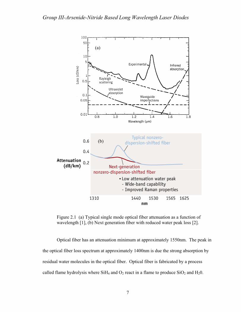
intramodal dispersion. Attenuation is dependent on wavelength as is shown in the Figure
2.1 below. The attenuation levels are extremely low compared to copper cable no matter
which wavelength is employed in the range of 700nm-1700nm. However, for distances
exceeding 500m the attenuation differences become significant.
6
Group III-Arsenide-Nitride Based Long Wavelength Laser Diodes
)
Figure 2.1 (a) Typwavelength [1], (b)
Optical fiber has an
the optical fiber loss spectr
residual water molecules in
called flame hydrolysis wh
(a
)
ic N
u
e
(b
al single mode optical fiber attenuation as a function of ext generation fiber with reduced water peak loss [2].
attenuation minimum at approximately 1550nm. The peak in
m at approximately 1400nm is due the strong absorption by
the optical fiber. Optical fiber is fabricated by a process
re SiH4 and O2 react in a flame to produce SiO2 and H20.
7

Group III-Arsenide-Nitride Based Long Wavelength Laser Diodes
Most of the H20 is extracted in the flame hydrolysis reactor in the gas phase but a small
amount can remain in the optical fiber resulting in the increased loss at 1400nm. The
level of H20 in the fiber cable is dependent on the manufacturing process. The fiber cable
manufacturing process has been improving steadily over the past several decades and
fiber can be produced today that has essentially removed the 1400nm loss peak [see
Figure 2.1]. However, there are millions of miles of fiber installed that have the large
loss peak at 1400nm. The fiber cable attenuation grows at shorter wavelength due to the
increasing efficiency of Rayleigh scattering with decreasing wavelength. At longer
wavelengths, molecular vibrations of the SiO2 molecule limit attenuation. Due the local
minima in fiber loss, wavelengths of 1310nm and 1550nm are commonly used in fiber
optic communications links.
Intermodal dispersion results from the excitation of more than one waveguide
mode of the optical fiber by the light source. As the different waveguide modes of the
optical fiber propagate at slightly different velocities, a single pulse input to the fiber will
then appear as a series of increasingly delayed pulses at the output. The net effect of this
intermodal dispersion is a broadening in time of the initial pulse potentially leading to
overlap with other data pulses and error generating intersymbol interference. The logical
approach to overcome intermodal dispersion is to employ optical fiber where there is a
single optical mode. By reducing the diameter of the optical fiber core (relative to the
wavelength of light), a single waveguide mode can be achieved eliminating the
intermodal dispersion. Common single mode fiber typically has a core diameter of about
9µm while multimode fiber is typically 50µm or 62.5µm. Alignment tolerances to
achieve less than 10% coupling loss are tighter than 1um for single mode fiber while they
8

Group III-Arsenide-Nitride Based Long Wavelength Laser Diodes
approach 10µm for multimode fibers. The use of single mode optical fiber is not
practical in many cases because of the required expensive, high precision optics to couple
laser light into the fiber or couple one fiber to another fiber.
To minimize the effects of intermodal dispersion in multimode fibers, the fiber is
fabricated with a graded refractive index profile. The graded index profile is designed to
minimize the differences in velocity of the different optical modes assuming a particular
wavelength and mode excitation. Most of the installed graded index fiber was designed
to be optimum at 1300nm with a uniform mode excitation (all modes excited) for use
with 1300nm LEDs.
Intramodal dispersion is present in single mode and multimode fibers and results
from differences in propagation velocity with optical wavelength. There are two sources
of intramodal dispersion in optical fiber, (i) inherent material dispersion and, (ii)
waveguide dispersion that depends on the waveguide geometry. The material dispersion
is due to the refractive index of the silica glass material varying with wavelength while
the waveguide dispersion is due to the wavelength to waveguide size ratio varying.
Optical pulses sent with laser light that is not perfectly monochromatic will suffer pulse
broadening due to the chromatic intramodal dispersion. Lasers that operate with multiple
modes will emit light at several different frequencies which will propagate with different
velocities. Even single mode lasers are not perfectly monochromatic as they have an
inherent laser linewidth (i.e. range of spectral content) which is further broadened
spectrally by wavelength chirp effects under modulation. Figure 2.2 shows a plot of the
dispersion for single mode optical fiber.
9

Group III-Arsenide-Nitride Based Long Wavelength Laser Diodes
Figure 2.2 Single mode optical fiber dispersion as a function of wavelength [1].
The material dispersion (ps/nm-km) is zero at approximately 1270nm and has a
positive slope while the waveguide dispersion is always small and negative with a
negative slope. The total dispersion has a zero at 1310nm as shown in Figure 2.2.
2.1.2 Semiconductor laser sources
The properties and performance of the semiconductor lasers used in optical
communication links are determined by the materials from which they are fabricated and
the type of laser structure created in the fabrication process. Semiconductor lasers are
formed by growing high quality single crystal layers on a single crystal substrate in a
process known as epitaxy. To be able to grow the needed high quality layers, there must
be a close match to the lattice constant of the substrate material and a compatible
chemistry between the various layers of the laser structure. The operating wavelength
range of a semiconductor laser is determined by the bandgap of the semiconductor
10

Group III-Arsenide-Nitride Based Long Wavelength Laser Diodes
material used to fabricate the laser. Figure 2.3 below is a plot of the bandgap of common
semiconductor laser materials versus their lattice constant. Common substrates for laser
fabrication are GaAs and InP.
0
0.5
1
1.5
2
2.5
5.5 5.6 5.7 5.8 5.9 6 6.1 6.2
GaAs
AlAs
InAs
InxGa
1-xAs
AlxGa
1-xAs
InxAl
1-xAs
InP
980nm
1300nm
1550nm
InxGa
1-xAs
yP
1-y
Ene
rgy
Gap
(eV)
Figure 2.3 Energy gap versus lattice constant for group III-V semiconductors. Lattice Constant (Å)
For materials grown on a GaAs substrate, the laser operating ranges are approximately
650-980nm range while those grown on InP substrates operate in the 1200-1600nm
range. The long wavelength limit of the conventional GaAs based materials is due to the
maximum amount of indium that can be incorporated before strain related defects form
due to the increasing lattice constant as indium is added to GaAs.
As detailed in the previous section, lasers operating in the range of 1300-1600nm
range are important for single mode optical fiber transmission due to the superior
transmission performance at these long wavelengths. Therefore, InP based lasers have
been used for all single mode optical fiber communications systems.
11
Group III-Arsenide-Nitride Based Long Wavelength Laser Diodes
An important property of semiconductor lasers is their ability to operate over a
wide range of temperatures. In most communications applications, the transceiver
module that contains the laser diode must be able to operate from –5ºC to +85ºC to allow
for changes in temperature of the environment as well as the heat from large amount of
other electronics and optoelectronics typically found in an equipment rack or closet. Two
issues are of importance for operating over the required temperature range, wavelength
stability and optical output power. For all semiconductor lasers, the emission wavelength
depends strongly on the temperature because the laser cavity refractive index (i.e. the
semiconductor material) depends on temperature. For single mode lasers the shift in
emission wavelength with temperature is typically 0.1nm/°C while that for multimode
lasers is about 5X larger. Such wavelength shifts with temperature are problematic for
Wavelength Division Multiplexed (WDM) systems where the optical spectrum is divided
into narrow wavelength channels that are only a few tenths of a nanometer wide. For the
shorter wavelength, GaAs based lasers that operate in the range of 700-1000nm,
operation with high output power over this temperature range is typically not a problem.
However, the InP based lasers that currently dominate the 1300nm and 1550nm fiber
transmission window applications are more challenged at the higher temperatures as will
be discussed in upcoming chapters. So, for WDM lasers or high power InP based lasers
constant chip operating temperature is needed and a thermoelectric cooler is employed.
However, the use of a thermoelectric cooler is very costly both in initial component cost
as well as operating cost over the life of the transceiver. Thermoelectric coolers are
expensive, generally costing 2-10 times the price of the laser chip itself. The power
required to operate the thermoelectric cooler also tends to dominate the total power
12

Group III-Arsenide-Nitride Based Long Wavelength Laser Diodes
consumption of the transceiver module. Finally, a thermoelectric cooler limits the
minimum size of packaged laser module. For example, a typical single mode laser diode
chip might dissipate approximately 100-200mW of power due to drive current and
voltage while a thermoelectric cooler to maintain such a chip at 25ºC with an 85ºC
ambient could dissipate 4W of power. Such a power draw is not only problematic from
the standpoint of the cost of supplying the additional power, but also having to remove
that much heat from an equipment rack can become the factor limiting component
density. Much larger floor spaces with more sophisticated cooling systems are required
to employ cooled lasers compared with their uncooled counterparts. Uncooled lasers are
therefore very important in the LAN and MAN applications because their lower power
dissipation and initial cost are crucial to market success.
The thermal performance of a laser diode is determined by the changes in optical
loss with temperature and changes in the average carrier concentration in the active
region for a given amount of current. Generally, the optical loss (particularly at long
wavelength) increases with temperature while a lower electrical carrier concentration is
achieved in the active region with increased temperature. GaAs based materials have
demonstrated significantly better thermal performance than the InP based materials. As
such, the short wavelength GaAs based lasers have been able to make high performance
lasers that operate over the required temperature range. Unfortunately, 1550nm InP
based lasers generally require thermoelectric coolers while those at 1310nm are available
with and without coolers depending on performance needs. Much effort has been
focused on producing 1310nm lasers with out thermoelectric coolers over the past 10-
13

Group III-Arsenide-Nitride Based Long Wavelength Laser Diodes
15years, particularly in Japan, and this effort presses the limits of materials and
fabrication technology.
The wavelength purity of a semiconductor laser is important in communications
systems as multiple wavelength emission results in increased modal dispersion, pulse
broadening, and mode partition noise. The structure of the laser diode determines the
frequency purity of the laser. In edge-emitting laser diodes, it is relatively simple to
fabricate single transverse mode waveguides from the semiconductor materials through
the combination of epitaxial layer design and photolithography and etching. However, to
restrict the laser operation to a single longitudinal mode the formation of complex grating
structures (as in a DFB laser) is required. The grating has a narrow pass band which can
select just one of the longitudinal modes of the Fabry-Perot resonator. Because of the
added complexity of the grating formation step, and the associated increase in
manufacturing cost, multi-longitudinal mode Fabry-Perot lasers are often used despite the
performance loss relative to a single mode laser. In the case of surface emitting lasers,
single longitudinal mode operation is easily achieved because the short cavity length
results in a wide cavity mode spacing, yielding only a single longitudinal mode within the
gain spectrum of the quantum well gain region. By decreasing the surface emitting laser
waveguide diameter (device diameter) single transverse mode operation can also be
achieved, but with somewhat decreased power performance due to heating and/or optical
loss.
The ability to couple the light from the laser to an optical fiber is crucial to both
cost and performance. As detailed above, the alignment tolerance to couple light into a
single mode fiber is very stringent compared to that of a multimode fiber due the size of
14

Group III-Arsenide-Nitride Based Long Wavelength Laser Diodes
the fiber core. The high precision optics and costly alignment procedure determine much
of the product cost for a laser diode packaged module. However, the fiber type is the not
the only determining factor in ease of fiber coupling. The size of the optical mode in the
semiconductor waveguide also determines the ease of fiber coupling as the mode must be
matched by the coupling optics to the fiber mode. For example, the mode of a single
mode fiber is circularly symmetric with a diameter of the order of 10µm. In the case of
an InP edge emitting laser diode, the waveguide mode might typically be 5µm by 2µm in
size. The small mode size results in a highly divergent beam and the asymmetry results
in poor coupling efficiencies unless complex (and expensive) lenses are used to reshape
the semiconductor waveguide mode to produce a circular beam. Edge emitting laser
diodes therefore generally have maximum coupling efficiencies around 50% and involve
alignment of components with sub-micron accuracy. As surface emitting lasers can be
fabricated with circular mode shapes that range in diameter from several microns in the
case of single transverse mode devices to several tens of microns for multimode devices,
coupling ease and efficiency are greatly increased relative to edge emitters for both single
and multimode cases. Currently, there is extensive work in developing designs and
processes to change the mode size at the end of the edge emitting laser by complex
etching and regrowth to enable easier fiber coupling. This is an interesting case of
increasing chip cost to decrease overall product cost but surface emitting lasers avoid this
complexity completely.
At present, for high performance single mode optical links over long distances in
the fiber backbone and high bit-rates, edge-emitting, single mode DFB lasers are used
exclusively. The higher cost to achieve reasonable coupling efficiencies and to employ
15

Group III-Arsenide-Nitride Based Long Wavelength Laser Diodes
thermoelectric coolers is offset by the high performance (Gb/s/km) of the network.
However, uncooled multimode surface emitting and edge emitting lasers are used in
lower cost single mode and multimode LAN and MAN applications. High costs are
avoided in these applications when edge emitting lasers are used by simply accepting
very low (5-10%) coupling efficiencies. As the edge emitting lasers generally are
capable of much higher output powers than surface emitting lasers, similar fiber coupled
power can be achieved at the expense of overall efficiency.
2.2 Optical Fiber Link Applications in Networks
The nature of a fiber optic network depends greatly on the purpose and owner of
the network. There are two general classes of networks, private networks where the
owners of the network use the network for their own data transmission and public
networks where the owners sell the transmission bandwidth to others. The distinction
between private and public determines the basic nature of the communications protocols
used in each type of network. In private networks, sharing of resources is very common
to achieve high performance with little amount of overhead or network monitoring and
control. In contrast, as the bandwidth is ultimately sold, public networks emphasize
quality of service, performance monitoring, and control to enable customers to be assured
that they are receiving the performance for which they have paid.
Standards play an important role in the equipment and protocols used in both
public and private networks as they ensure that certain levels of performance should be
achievable and provide a basis of comparison for different equipment vendors so that
competition can exist and yield the best products at the lowest costs. Although the
16
Group III-Arsenide-Nitride Based Long Wavelength Laser Diodes
previous discussion indicated the relative merits of different types of fiber and lasers,
many other factors come into play in determining the physical hardware (including fiber
and laser source) including compatibility with existing equipment, performance of other
network components, safety, and politics. Because of the many factors involved in
establishing a standard, a technology may be chosen which is less than the best from a
performance perspective. However, once a standard is established nearly all vendors
produce only equipment or components consistent with the standard.
In public networks, the most important standard is SONET/SDH. The physical
interface for SDH specifies for single mode optical fiber various loss and dispersion
budgets for different laser types (single mode or multi-longitudinal mode) and
wavelengths (1310nm or 1550nm) for different link lengths and bit-rates. No short
wavelength lasers (850 or 980nm, for example) are in the standard and 1310nm lasers
dominate the short distance links <15km.
The 1310nm laser is used in a transponder in the optical line terminal to convert
the long distance (usually WDM) 1550nm light to short reach (SR) 1310nm light for
distribution to other networking equipment with SR interfaces such as optical cross-
connects or SONET electrical add-drop multiplexers. The reason why 1310nm is used
over short wavelength lasers is that single mode fiber is multimode at short wavelengths
(<1200nm) and higher optical powers at longer wavelengths are permitted by eye safety
standards. The eye safety standard is particularly important in such intra-office
applications due to the shear number of fibers in such an environment and the cost of the
trained technicians who can handle work with links that break the eye safety limits.
17

Group III-Arsenide-Nitride Based Long Wavelength Laser Diodes
Compared with 1550nm lasers, the 1310nm SR lasers are uncooled allowing much lower
total laser module power dissipation for the system.
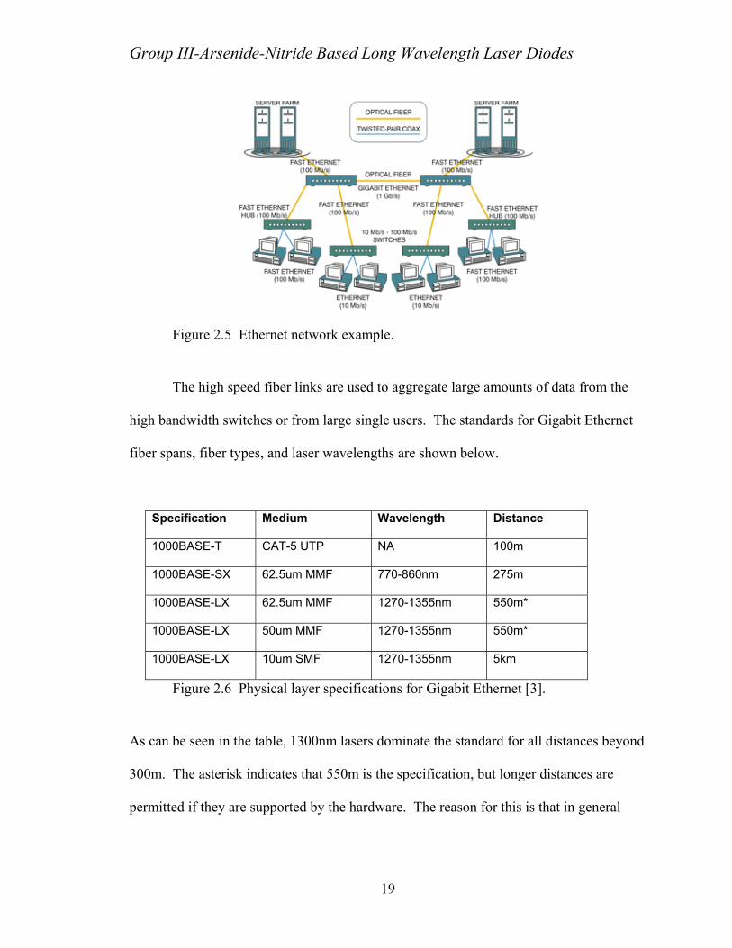
In private networks, the most important standards are Ethernet/Gigabit-Ethernet
for local area networks and (LANs) and Fibre-Channel for storage area networks (SANs).
The application relationship to these LANs, SANs, and the public wide area and
metropolitan are networks (WANs, MANs) is depicted in the figure below.
Figure 2.4 Network relationship SAN,LAN, MAN/WAN.
The Fibre-Channel standards are relatively compatible with the Gigabit Ethernet
standards and similar hardware choices are made. In Gigabit Ethernet, 1Gb/s data rates
are supported between Ethernet switches and terminal equipment as depicted below.
18
Group III-Arsenide-Nitride Based Long Wavelength Laser Diodes
Figure 2.5 Ethernet network example.
The high speed fiber links are used to aggregate large amounts of data from the
high bandwidth switches or from large single users. The standards for Gigabit Ethernet
fiber spans, fiber types, and laser wavelengths are shown below.
Specification Medium Wavelength Distance
1000BASE-T CAT-5 UTP NA 100m
1000BASE-SX 62.5um MMF 770-860nm 275m
1000BASE-LX 62.5um MMF 1270-1355nm 550m*
1000BASE-LX 50um MMF 1270-1355nm 550m*
1000BASE-LX 10um SMF 1270-1355nm 5km
Figure 2.6 Physical layer specifications for Gigabit Ethernet [3].
As can be seen in the table, 1300nm lasers dominate the standard for all distances beyond
300m. The asterisk indicates that 550m is the specification, but longer distances are
permitted if they are supported by the hardware. The reason for this is that in general
19

Group III-Arsenide-Nitride Based Long Wavelength Laser Diodes
distances of 750m are possible but due to manufacturing defects in a large amount of
installed fiber the target distance is limited to 550m.
2.3 Optical Fiber Links Conclusion
The highest performance optical links would operate at either 1550nm or 1310nm
depending on the distance and bit-rate and employ single mode optical fiber. The
1550nm wavelength would be favored for longer distances due to the lower attenuation
(attenuation limited transmission) while the 1310nm would be favored at higher bit-rates
due to the lower chromatic dispersion (intramodal dispersion limited transmission). The
lowest performance, but lowest cost, is the graded index multimode fiber employing short
wavelength 700-850nm lasers. The performance is limited by both attenuation and
intermodal dispersion. The low cost is due to the use of the low cost GaAs VCSELs, Si
photodiodes, and low tolerance optical coupling.
As can be seen in the Gigabit-Ethernet standard, the lowest cost, lowest
performance choice was made for the shortest fiber links. However, all other link lengths
in Gigabit Ethernet and all of the short distance links in SONET/SDH specify 1310nm
lasers in either multimode or single mode fiber despite the higher cost of the laser sources
due to the performance requirements.
However, the above discussion leads to several possible improvements in laser
sources that could enable higher performance, lower cost optical links. A low cost
multimode 1310nm laser would be enable both lower cost and significant increases in
system performance when multimode fiber is employed. Additionally, a single mode
1310nm laser that is capable of lower cost single mode optical coupling and cooler-less
20

Group III-Arsenide-Nitride Based Long Wavelength Laser Diodes
operation would enable higher performance low cost single mode links. Research to
develop lasers capable of meeting these goals is described in this thesis.
21

Group III-Arsenide-Nitride Based Long Wavelength Laser Diodes
Chapter 3 Laser Background
3.1 Lasers
Any laser device consists of two essential components, a resonator and a gain
medium. The resonator stores electromagnetic energy typically by reflecting the fields at
its boundaries. The total electromagnetic field inside the resonator consists of the sum of
all of the fields within the resonator and reaches a maximum intensity when the fields add
in phase or constructively interfere. At the frequencies where strong field strengths are
enforced by the interference resonator modes exist. The electromagnetic fields are
generally periodic in both time and space inside of the resonator which results in
resonator modes existing periodically in frequency. All resonators have loss, either from
imperfect reflection at the resonator boundary or attenuation of the field by absorption by
the resonator medium. For the laser device, not all of the resonator or optical loss is
parasitic, as part of the transmission loss produces the useful output of the laser. The
amount of useful loss or output coupling relative to the amount of total optical loss
(output + parasitic loss) is a component of the efficiency of the laser.
22

Group III-Arsenide-Nitride Based Long Wavelength Laser Diodes
The gain medium, under the appropriate conditions, can amplify or increase the
intensity of a propagating electromagnetic wave. The amplification is provided by
stimulated radiative relaxation of excited states of the gain medium. For example, a
photon stimulates the relaxation of an excited electronic state of an atom or
semiconductor material through emission of another identical photon. The process of
creating the excited states of the gain medium is known as the pumping process. The
stimulated emission process is the exact inverse of the stimulated absorption process
where a ground state energy level is excited to a higher energy level by the absorption of
a photon. The relative amounts of total stimulated absorption and emission by the gain
medium is related to the number of species in the excited and ground states. Normally, a
medium has fewer excited state species than ground state species because of
thermodynamic statistics and the material has net absorption. However, under very large
pumping, the excited state population can be large enough to achieve a population
inversion where there are more excited state species than ground state species and net
emission or amplification can occur. As the gain properties of a medium are related to
some type of electronic energy state of the medium, the amount of gain varies with
optical frequency. For example, in many gas lasers the frequency range over which there
is significant gain is very small due to the narrow atomic resonance of the excited gas
species while in semiconductor lasers, the gain spectrum can be many orders of
magnitude larger due to the “banded” electronic structure of the semiconductor media
consisting of many electronic states over a wide range of energies.
In the laser device, the gain medium is placed within the resonator so that it can
amplify the stored energy. If the pump is sufficiently large to make the gain strong
23
Group III-Arsenide-Nitride Based Long Wavelength Laser Diodes
enough to offset all of the losses of the resonator, the electromagnetic field inside the
laser resonator grows to very large amplitudes and the laser is said to have reached lasing
threshold. The field strength can not grow infinitely large because the large
electromagnetic fields can use up or decrease the population of the excited states of the
gain medium faster than the pump can replenish them and the net gain saturates to unity.
The laser efficiency is generally the amount of energy coming out of the laser divided by
the amount of energy put into the laser (usually in the form of the pump). The efficiency
can be divided into the efficiency of pumping, which the percentage of the pump energy
that results in stimulated photons, and the optical efficiency which, as mentioned above,
is the percentage of photons that are lost as useful transmission relative to the total lost
photons.
3.2 Semiconductor Laser Gain Media
In semiconductor materials, the electronic states of the constituent atoms couple
together to form “bands” of electronic states that are separated from each other by “band-
gaps”. The fundamental electronic transitions in the optical frequency range are
generally between two different bands of electronic states. In a semiconductor, the lower
band, the valence band, is completely filled with electrons and the upper band, the
conduction band, is completely empty at absolute zero temperature. The behavior of the
electrons within the energy bands can be approximated by assuming they behave like free
electrons (in a gas) with an altered mass, the effective mass, which takes into account the
interactions of the electrons with the lattice. The electron energy as a function of
wavenumber is then parabolic with a curvature that depends on the effective mass. The
24
Group III-Arsenide-Nitride Based Long Wavelength Laser Diodes
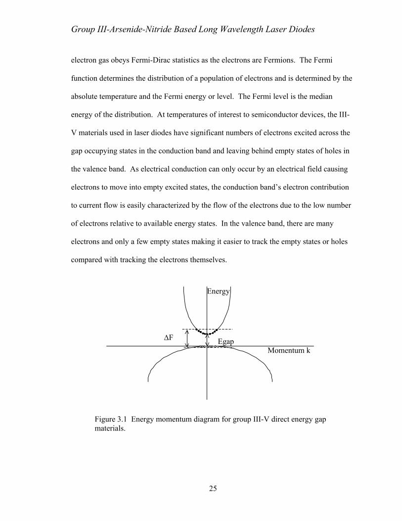
electron gas obeys Fermi-Dirac statistics as the electrons are Fermions. The Fermi
function determines the distribution of a population of electrons and is determined by the
absolute temperature and the Fermi energy or level. The Fermi level is the median
energy of the distribution. At temperatures of interest to semiconductor devices, the III-
V materials used in laser diodes have significant numbers of electrons excited across the
gap occupying states in the conduction band and leaving behind empty states of holes in
the valence band. As electrical conduction can only occur by an electrical field causing
electrons to move into empty excited states, the conduction band’s electron contribution
to current flow is easily characterized by the flow of the electrons due to the low number
of electrons relative to available energy states. In the valence band, there are many
electrons and only a few empty states making it easier to track the empty states or holes
compared with tracking the electrons themselves.
Egap ∆F Momentum k
Energy
Figure 3.1 Energy momentum diagram for group III-V direct energy gap materials.
25
Group III-Arsenide-Nitride Based Long Wavelength Laser Diodes
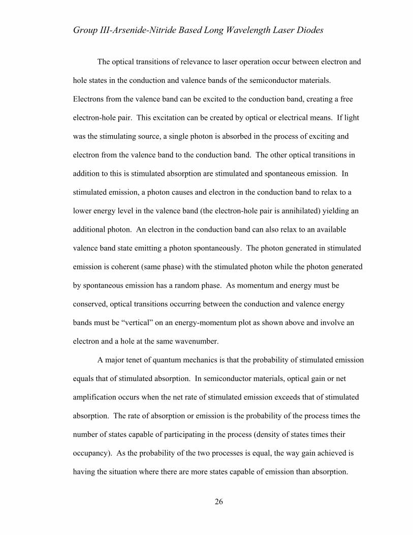
The optical transitions of relevance to laser operation occur between electron and
hole states in the conduction and valence bands of the semiconductor materials.
Electrons from the valence band can be excited to the conduction band, creating a free
electron-hole pair. This excitation can be created by optical or electrical means. If light
was the stimulating source, a single photon is absorbed in the process of exciting and
electron from the valence band to the conduction band. The other optical transitions in
addition to this is stimulated absorption are stimulated and spontaneous emission. In
stimulated emission, a photon causes and electron in the conduction band to relax to a
lower energy level in the valence band (the electron-hole pair is annihilated) yielding an
additional photon. An electron in the conduction band can also relax to an available
valence band state emitting a photon spontaneously. The photon generated in stimulated
emission is coherent (same phase) with the stimulated photon while the photon generated
by spontaneous emission has a random phase. As momentum and energy must be
conserved, optical transitions occurring between the conduction and valence energy
bands must be “vertical” on an energy-momentum plot as shown above and involve an
electron and a hole at the same wavenumber.
A major tenet of quantum mechanics is that the probability of stimulated emission
equals that of stimulated absorption. In semiconductor materials, optical gain or net
amplification occurs when the net rate of stimulated emission exceeds that of stimulated
absorption. The rate of absorption or emission is the probability of the process times the
number of states capable of participating in the process (density of states times their
occupancy). As the probability of the two processes is equal, the way gain achieved is
having the situation where there are more states capable of emission than absorption.
26

Group III-Arsenide-Nitride Based Long Wavelength Laser Diodes
This condition when there are more states capable of emission than absorption is often
referred to as “population inversion”.
For the (undoped) active region of a laser diode, at thermal equilibrium the
electron and hole populations ( or “gases”) in the conduction and valence bands are equal
and the Fermi level lies within the energy gap. If a stream of photons is incident on the
material, the probability of stimulated emission for a single electron in the conduction
band is equal to that of stimulated absorption for a single electron in the valence band.
But, because there are so many more electrons in the valance band than in the conduction
band, the net result will be absorption of a stream of incident photons. If the system can
be forced away from equilibrium by injecting electron-hole pairs through electrical or
optical pumping the situation can be changed and net gain created. When the system is
forced away from equilibrium, the carriers can come into thermal equilibrium with the
lattice very rapidly because intraband relaxation can occur on the picosecond time scale.
However, interband relaxation (which involves the relevant optical processes) occurs on
the nanosecond time scale. Because of this large asymmetry between intra- and inter-
band relaxation, two separate Fermi functions with separate Fermi levels (often called
“quasi-Fermi levels”) can be employed which represent the occupation of the states
within each band for the carriers. With increasing pumping, the quasi-Fermi levels
depart further from the equilibrium Fermi level within the energy gap. As mentioned
earlier, the quasi-Fermi levels represent the median energy of the carrier populations. At
the Fermi level there is 50% probability of occupancy. If the pumping of the active
region is sufficient to achieve a quasi-Fermi level separation that is larger than the energy
of an incident photon, then for a given wavenumber there will be more occupied electron
27

Group III-Arsenide-Nitride Based Long Wavelength Laser Diodes
states in the conduction band than in the valence band. Therefore, the probability of net
stimulated emission will be larger than that for absorption and optical gain (ignoring loss)
can be achieved. For an excellent discussion of the physics of optical gain in atoms and
semiconductors refer to reference [4].
There are several ways to achieve the high levels and electrons and holes needed
to achieve optical gain in semiconductor materials. The simplest conceptually is to
“photo-pump” the material, by using intense light energy to excite electrons from the
valence band to the conduction band. If the photon flux is sufficiently large and the
lifetime of the excited electrons is long enough, then a population inversion can be
achieved. However, from the standpoint of a making a device that is practical, it is better
to use current injection through a pn junction to achieve the high levels of electrons and
holes needed in the semiconductor medium (as an additional light source is not needed).
To efficiently generate high concentrations of carriers, the active region is placed
in the center intrinsic region of a double heterostructure pin diode. The diode structure
results in a large injection of electrons and holes from the n and p layers respectively into
the intrinsic region where the gain or active layer is contained. Heterojunctions are
employed in the diode to effectively confine the electrons and holes to the intrinsic region
so that they can participate in radiative transitions instead of being injected as minority
carriers into the doped regions (where they will recombine either through spontaneous
emission or non-radiatively). Confining carriers to a small volume reduces the quantity
of injection current needed to achieve population inversion. It is common to restrict the
volume of the active materials to small enough volumes by growing the layers thin
enough that quantum confinement energies become greater than kT at the operating
28

Group III-Arsenide-Nitride Based Long Wavelength Laser Diodes
temperature and must be taken into account in designing the laser device. These quantum
well structures have added benefits due to the statistics of the 2D electron gas properties
compared with the statistics of the 3D bulk material [5]
p-type
n-type
i or undoped
Ec
Ev
Fp
Fn
hν > Εg Eg
Figure 3.2 Energy band diagram for laser diode active region. Electrons from the n-type material and holes from the p-type material are injected into the narrower bandgap active layer where they are “trapped” by the surrounding heterojunctions and efficiently recombine yielding a photon.
In an ideal laser diode, as opposed to an ideal conventional diode, very few
carriers actually surmount the barriers and become minority carriers. In the analysis of
diodes this recombination of carriers in the depletion regions can be shown to result in a
diode ideality factor of about 2. The current that injects carriers into the intrinsic and
active regions is the pump mechanism in semiconductor laser diodes. The pump
efficiency of a semiconductor laser diode is therefore related to the percentage of carriers
that are injected into the active region and result in stimulated photons. The laser diode
pump efficiency is more commonly called the internal or injection efficiency. Non-
radiative recombination processes and carriers leaking over or surmounting the
heterojunction barriers of the diode cause a reduction in the internal efficiency. Typical
internal efficiencies can be about 80% and gains of several thousand per centimeter can
29

Group III-Arsenide-Nitride Based Long Wavelength Laser Diodes
be achieved with semiconductor laser materials. The size of the heterojunction barriers
surrounding the laser active region is determined by the materials used. The larger
barrier heights of the GaAs based devices relative to those in InP devices is one the key
contributors to the superior performance of GaAs based devices relative to InP devices at
elevated temperature.
As the current injected into the active region of the laser device increases from
zero, it first reaches a level where a population inversion is created and the active
material begins to amplify the light inside of the laser resonator. At some current
injection level beyond achieving population inversion, the active layer carrier density has
reached the point that sufficient optical gain is produced to overcome both the waveguide
and mirror reflection losses. When this threshold current is reached, any further increase
in injected current (current multiplied by the injection efficiency) results in stimulated
photon emission. The laser output power beyond threshold is the terminal current
multiplied by the injection and optical efficiencies.
3.3 Edge-Emitter Laser Diodes
Semiconductor lasers are generally formed by a combination of crystal growth
and semiconductor processing techniques such as photolithography, etching, and
dielectric or metal deposition. The crystal growth step allows the layering of very thin,
high quality single crystal layers with varying compositions on a substrate. The materials
that can be grown generally have different material parameters such as energy gaps,
refractive indices, and doping or conductivity type. In an edge-emitter or in-plane laser
diode, an optical waveguide with an embedded active region is formed during the crystal
30

Group III-Arsenide-Nitride Based Long Wavelength Laser Diodes
growth step. The layers are doped such that the active region is within a pin
heterojunction diode. Because of the Kramers-Kronig relationship between the real part
of the refractive index or dielectric constant and the imaginary part (the loss coefficient
which turns on at the energy gap), materials with wide energy gaps tend to have small
refractive indices. In the laser diode, the waveguide cladding layers need to have lower
refractive indices than the core of the wavguide to have good low optical loss
waveguiding by total internal reflection. The cladding layers will therefore have larger
energy gaps than the core layers by the Kramers-Kronig relations (within in a given
material system). Fortunately, this is desirable from the electrical standpoint because the
wider energy gap layers create the barriers needed to prevent carrier leakage out of the
active layers and results in the layers being transparent to the laser light.
The waveguide is terminated on both ends by cleaving the semiconductor wafer
along crystal planes to result in atomically smooth and abrupt interfaces. The abrupt
interface acts as a mirror and provides the reflection to form the resonant cavity. Because
the refractive indices of the compound semiconductors and the mode index of the
waveguide modes all tend to be around a value of 3.5, the air-semiconductor interface of
the cleaved facet results in about 30% power reflectivity or about 70% power
transmission. The resonator therefore consists of a low loss waveguide (due to the total
internal reflections at the waveguide boundaries) which suffers transmission losses of
70% at each end of the device. If the intensity of the light is normalized to unity just
before the 70% transmission loss at the cleaved mirror facets the field intensity is 0.3
after transmission. For the gain to offset the loss, the gain must amplify the intensity of
0.3 back up to unity. The single pass gain needs to be about 1/0.3 or about 300%. This
31
Group III-Arsenide-Nitride Based Long Wavelength Laser Diodes
large amount of gain is achievable because the gain region fills the entire length of the
edge-emitter laser cavity.
The dimensions of typical edge-emitter laser diodes are in the range of 2-40µm in
width and 200-1000µm in the length. Because the waveguide core is usually around
0.1µm in thickness the light coming from the edge-emitter is highly elliptical. The light
diverges much more quickly from the thin waveguide thickness than from the modest
waveguide width. In order to efficiently couple the light into a round optical fiber, which
typically has a narrow range of acceptance angles, external lenses and optics are required
to reshape the laser light beam.
The laser device is restricted in width or diameter to confine the current flowing
to and carrier density in the active region and to provide additional waveguiding. The
portion of the active region that is pumped via current is restricted by either restricting
current flow by etching the upper cladding layers (ridge laser) or by etching through the
active region and growing higher bandgap semiconductor material around it (buried
heterostructure lasers).
Because of the relatively long length of the edge-emitter lasers (compared to the
wavelengths of light) there are many closely spaced Fabry-Perot or cavity resonances
within the gain spectrum of the active region. The laser operates at the peak gain
wavelength of the active region since this is the wavelength where the gain first equals
the loss.
The edge emitting structure results in a rather favorable situation when it comes to
dissipating power. The geometry of a long narrow ridge sitting on a thermally massive
substrate results in a relatively low thermal impedance (the rise in temperature of the
32

Group III-Arsenide-Nitride Based Long Wavelength Laser Diodes
ridge for a given power dissipated in the ridge). Thermal impedance is a very important
parameter for laser performance as the active region is generally very sensitive to
temperature. To describe the thermal performance of a laser structure the following
equation is often used [5].
00
TT
th eII =
The above exponential dependence on temperature is not derivable from any fundamental
physics and is based on phenomenological behavior. However, laser and semiconductor
physics does dictate that at higher temperatures, optical losses increase, non-radiative
recombination rates increase, distributions in energy smear out making a higher
percentage of electrons capable of surmounting confining potential barriers and reducing
the density of carriers (and gain) and a given energy.
3.4 Vertical Cavity Surface Emitting Lasers
Vertical Cavity Surface Emitting Lasers diodes or VCSELs differ from edge-
emitter lasers in the geometry of the laser cavity. The light propagates normal to the
plane of the wafer and all of the layers grown by epitaxy. The light therefore comes out
of the surfaces of the wafer and not the edges. However, the active region has the same
geometry as the edge-emitter so the optical mode is now propagating perpendicular to the
active layers. Current is typically driven through the mirror sections with contacts on the
topside and backside of the device wafer. Light emission can be from the top or bottom
of the device depending on the relative transmission of the two mirrors.
33
Group III-Arsenide-Nitride Based Long Wavelength Laser Diodes
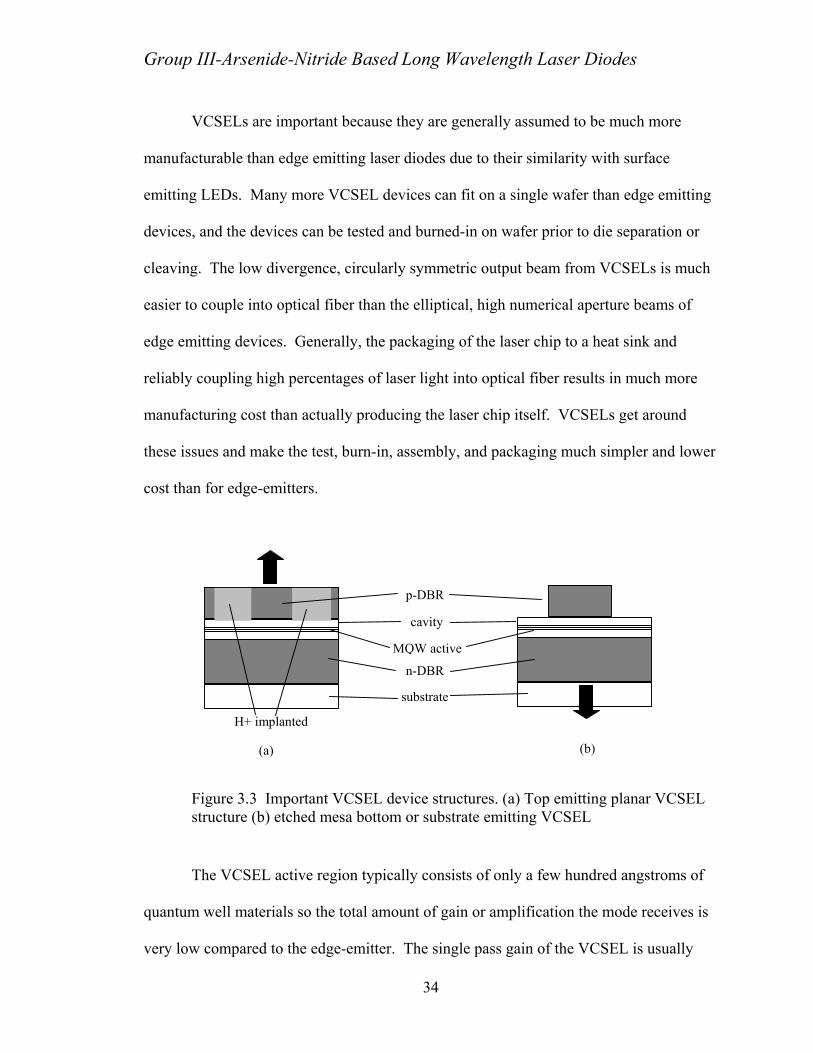
VCSELs are important because they are generally assumed to be much more
manufacturable than edge emitting laser diodes due to their similarity with surface
emitting LEDs. Many more VCSEL devices can fit on a single wafer than edge emitting
devices, and the devices can be tested and burned-in on wafer prior to die separation or
cleaving. The low divergence, circularly symmetric output beam from VCSELs is much
easier to couple into optical fiber than the elliptical, high numerical aperture beams of
edge emitting devices. Generally, the packaging of the laser chip to a heat sink and
reliably coupling high percentages of laser light into optical fiber results in much more
manufacturing cost than actually producing the laser chip itself. VCSELs get around
these issues and make the test, burn-in, assembly, and packaging much simpler and lower
cost than for edge-emitters.
p-DBR
(a) (b)
cavity
n-DBR
substrate
MQW active
H+ implanted
Figure 3.3 Important VCSEL device structures. (a) Top emitting planar VCSEL structure (b) etched mesa bottom or substrate emitting VCSEL
The VCSEL active region typically consists of only a few hundred angstroms of
quantum well materials so the total amount of gain or amplification the mode receives is
very low compared to the edge-emitter. The single pass gain of the VCSEL is usually
34
Group III-Arsenide-Nitride Based Long Wavelength Laser Diodes
less than 1%. Because the gain must be able to offset all of the losses to achieve lasing,
the optical losses in the VCSEL device must be very low. To keep the optical
transmission losses low, the VCSEL mirror reflectivities need to be very high, >99%.
With such low transmission losses, the parasitic optical losses due to absorption and
diffraction need to be extremely small to make an efficient laser device.
Because this thesis concerns novel long wavelength VCSEL devices, general
VCSEL issues will be explored further in the following sections. Long wavelength
VCSEL issues are discussed in Chapter 4. As they are the most developed of the VCSEL
devices, short wavelength (850-980nm) GaAs based VCSELs will be used as the
prototypical or baseline VCSEL structure in the following discussions.
3.4.1 VCSEL Mirror Optical Properties
To achieve mirror reflectivities greater than 99%, distributed mirrors based upon
multiple reflections from the interfaces between low loss materials with different
refractive indices need to be employed. Metals generally regarded as reflective do no
have reflectivities high enough to be used as VCSEL mirrors. For example, gold, a
highly reflective metal, has a reflectivity of only about 93%. The index discontinuities at
every interface between the layers of the distributed mirror gives rise to many small
reflections which can add coherently together if properly phase matched. If the thickness
of each mirror layer is chosen appropriately, all of the reflections can add in phase to
achieve a single large reflectivity over a range of wavelengths. The basic unit repeated in
the multilayer stack of the distributed mirror is a half wavelength thick structure
consisting of two layers with different refractive indices that are each a quarter of a
wavelength thick. The quarter wave thickness of each layer results in all reflections
35
Group III-Arsenide-Nitride Based Long Wavelength Laser Diodes
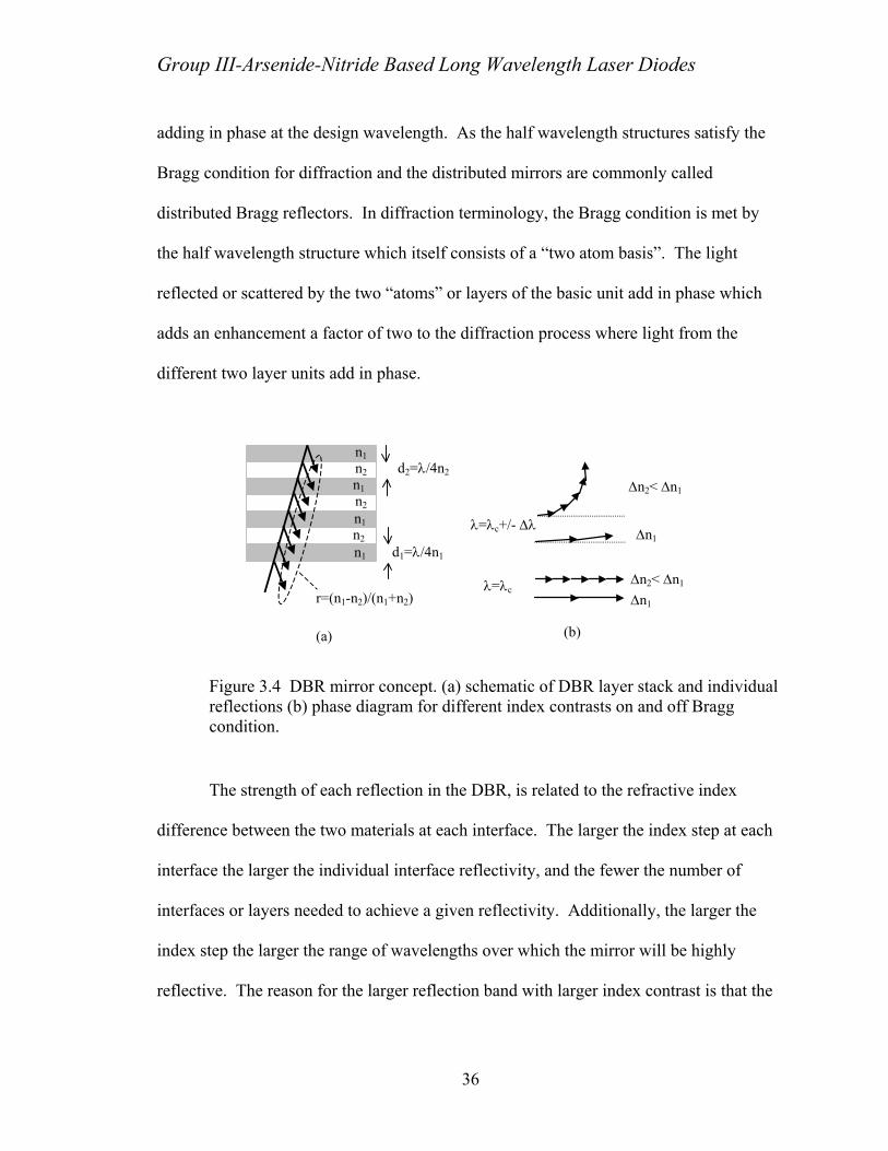
adding in phase at the design wavelength. As the half wavelength structures satisfy the
Bragg condition for diffraction and the distributed mirrors are commonly called
distributed Bragg reflectors. In diffraction terminology, the Bragg condition is met by
the half wavelength structure which itself consists of a “two atom basis”. The light
reflected or scattered by the two “atoms” or layers of the basic unit add in phase which
adds an enhancement a factor of two to the diffraction process where light from the
different two layer units add in phase.
n1
n2
n2
n2
n1
n1
n1
d1=λ/4n1
d2=λ/4n2
r=(n1-n2)/(n1+n2) ∆n1 ∆n2< ∆n1
∆n1
∆n2< ∆n1
λ=λc
λ=λc+/- ∆λ
(a) (b)
Figure 3.4 DBR mirror concept. (a) schematic of DBR layer stack and individual reflections (b) phase diagram for different index contrasts on and off Bragg condition.
The strength of each reflection in the DBR, is related to the refractive index
difference between the two materials at each interface. The larger the index step at each
interface the larger the individual interface reflectivity, and the fewer the number of
interfaces or layers needed to achieve a given reflectivity. Additionally, the larger the
index step the larger the range of wavelengths over which the mirror will be highly
reflective. The reason for the larger reflection band with larger index contrast is that the
36
Group III-Arsenide-Nitride Based Long Wavelength Laser Diodes
light effectively sees fewer mirror layers and the coherent addition of the individual
reflection phases has less of a filtering effect.
37

Group III-Arsenide-Nitride Based Long Wavelength Laser Diodes
1.0
0.8
0.6
0.4
0.2
0.0
Ref
lect
ivity
-400 -200 0 200 400Wavelength Detuning (nm)
∆n=0.1 ∆n=0.5 ∆n=1.0
0.0001
0.001
0.01
0.1
1
1-R
252015105Number of Mirror Pairs
1000
800
600
400
200
0
+/-0.05 dB Bandw
idth (nm)
∆n=0.1 ∆n=0.5 ∆n=1.0
Figure 3.5 DBR mirror simulation for 10 mirror pairs. Different refractive index contrasts are typical InP, GaAs, and dielectric materials respectively. (a) illustrates effect of refractive index contrast and (b) quantifies effect of refractive index contrast.
38

Group III-Arsenide-Nitride Based Long Wavelength Laser Diodes
3.4.2 VCSEL Short Cavity and Interference Effects
The optical length of the laser cavity in a VCSEL device is of the order of the
wavelength of light. The use of such a short cavity, or microcavity, is motivated by the
need to have minimal diffraction related optical losses and to have single longitudinal
mode laser operation. As the laser light is propagating normal to the semiconductor
wafer surface, there is not any lateral waveguiding in a VCSEL device. While there is
some waveguiding to the gain and temperature profiles in the VCSEL and recently the
use of dielectric apertures in the VCSEL mirrors aids in confining the optical mode,
lengthening the VCSEL cavity leads to rapidly increasing optical loss. The single
longitudinal mode operation minimizes the number of wavelengths emitted by the
VCSEL device (the lateral modes are closely spaced in wavelength), increasing its utility
in fiber optic communications systems. Finally, from a practical perspective, a long
VCSEL cavity would have to be grown into the device by the epitaxy process which
already is strained by the large amount of material needed to be grown for the two DBR
mirrors.
The short cavity length results in usually a single cavity resonance or Fabry-Perot
mode within the cavity spectrum. Unlike the Fabry-Perot edge-emitter which will
operate at the peak gain wavelength due to the nearly continuous distribution of optical
modes, the VCSEL will operate only at the single cavity mode if it has enough gain. For
optimal performance, the gain spectrum needs to be aligned to the cavity mode with a
tolerance of a few nanometers in wavelength which translates to a few nanometers in
thickness. Precise control of the growth layer thickness is required to be able to make
good devices. An in-situ optical reflection measurement is often used to achieve the tight
39

Group III-Arsenide-Nitride Based Long Wavelength Laser Diodes
tolerances required [6]. The growth sequence is stopped a hundred Angstroms or so
before the growth of the top mirror and the reflectivity spectrum is measured. With good
values for the optical constants of the device materials a simulation of the reflectivity
spectrum can be made accurately. Deviations from the desired spectrum can be corrected
by growing the rest of the cavity slightly longer or shorter than was originally planned in
the growth sequence.
As all of the layers of the VCSEL device have thicknesses on the order of the
wavelength of the light (or less), there are additional design issues in a VCSEL that are
different than in edge emitters. The operation of the distributed mirrors and the Fabry-
Perot laser cavity all rely on the interference of light resulting in an optical standing wave
or light intensity pattern that varies in space.
Figure 3.6 below is a simulation of the standing wave that develops in the VCSEL
mirror sections with different refractive index contrasts. Within the optical cavity that
would be sandwiched between two DBR mirrors in a VCSEL the standing wave would
be contiguous with the mirror standing waves.
40

Group III-Arsenide-Nitride Based Long Wavelength Laser Diodes
2.0
1.5
1.0
0.5
0.0
Inte
nsity
(rel
ativ
e to
inci
dent
)
543210Depth in Mirror (wavelengths)
high
low
refractive index
∆n=0.1 ∆n=0.5 ∆n=1.0
Figure 3.6 Standing wave optical intensity in the DBR mirror for various index contrasts. Note, the intensity can be larger than the intensity of the incident traveling wave due to constructive interference.
Optical transition rates, either absorption or gain, depend on the optical
intensity overlapping the active material [5]. The standing wave that develops in a
DBR mirror and VCSEL cavity therefore will affect the transition rates relative to
single pass traveling wave values. For example, if the gain medium, i.e. the quantum
wells, is placed at the nulls of the optical field, no optical gain would occur no matter
how large the carrier density of the quantum wells. Similarly, if the quantum wells
are placed at the maximum of the standing wave pattern, the gain the optical mode
experiences would be a factor of two larger than an active region that interacts with
the optical wave over many wavelengths (and hence averages over all the values of
intensity). In a similar manner, free carrier absorption losses in the DBR mirrors will
41
Group III-Arsenide-Nitride Based Long Wavelength Laser Diodes
depend greatly on the carrier density at the peaks of the standing wave which occur at
the interface between the two different mirror materials. As discussed in the next
section, free carriers can accumulate at the mirror interfaces and lead to larger than
expected optical losses.
3.4.3 DBR Mirror Electrical Issues
In most VCSELs, current is driven through the DBR mirror sections. The
heterojunctions in the mirrors result in increased electrical resistance due to the rectifying
nature of a heterojunction even if the doping type is constant through the junction. The
interfaces alternate between forward and reverse bias through the mirror structures. The
voltage drop at the reverse biased junctions is due to both energetic barriers due to the
energy gap differences that electrons or holes must surmount to permit conduction and
due to regions of depletion where the majority carrier density has be reduced significantly
due to charge transfer between the two different mirror layer materials. Generally,
majority carriers are transferred from the wider bandgap material to the narrower
bandgap material to equilibrate the Fermi levels in the two different materials.
The voltage drop at each mirror section can be catastrophic to operation, as
several volts to tens of volts can be dropped across the mirror leading to large electrical
power dissipation and resultant heating of the active region. Fortunately, it is possible to
theoretically eliminate the voltage drop at the DBR mirror layer interfaces and much
work has been done in designing structures where the voltage drop at the heterojunctions
is minimized [7, 8, 9].
The objective of minimizing the parasitic voltage drop in the VCSEL mirrors is
achieved by minimizing the potential barriers for carrier transport and ensuring carrier
42

Group III-Arsenide-Nitride Based Long Wavelength Laser Diodes
density profiles that are devoid of depletion at equilibrium and bias with sufficient
majority carriers to conduct the needed current. Additionally, regions of accumulation of
majority carriers can be problematic from an optical loss standpoint particularly in the p-
type mirror [8]. The mirror heterojunction design alters the interface region through
continuous compositional grading between the two materials and specific doping profiles.
The compositional grading results in the bandgap of the materials smoothly changing
from one layer to the other without the sharp peaks or valleys associated with the band
lineup (conduction and valence band offsets) and charge transfer across the junction to
align the Fermi levels associated with an abrupt junction. With a known compositional
grading function, the doping can be used to flatten the band of interest and yield a region
devoid of depletion.
P-type DBR mirrors are particularly problematic due to the low mobility of holes,
the high optical absorption associated with holes due to intra-valence band absorption,
and the concentration and growth temperature dependent diffusion of most p-type
dopants. Figure 3.7 below shows a simulation of an abrupt p-GaAs/p-AlAs
heterojunction with a nominally uniform 5x10¹⁷/cm3 hole concentration at 0V and at 2V
reverse bias. As can be seen in the plot, holes are transferred from the wide bandgap
AlAs to the narrow bandgap GaAs to equilibrate the Fermi levels. The charge transfer
and abrupt bandgap change results in a potential barrier in the valence band for hole
current flow and a depletion region in the first tens of nanometers of the AlAs. Under 2V
reverse bias, the depletion region and potential barrier increase. The current density at
this voltage is only 0.24A/cm2, far below the threshold current density and even farther
below what would be needed for a VCSEL drive current density. Even at the low
43

Group III-Arsenide-Nitride Based Long Wavelength Laser Diodes
threshold current densities of state of the art VCSELs, a p-type mirror with abrupt
interfaces would have >20V of potential drop.
-5.5
-5.0
-4.5
-4.0
-3.5En
ergy
(eV)
0.200.150.100.050.00Position (microns)
1012
1013
1014
1015
1016
1017
1018
Hole C
oncentration (1/cm3)
Ec
Ev
Hole Conc.
-5
-4
-3
-2
Ener
gy (e
V)
0.200.150.100.050.00Position (microns)
1011
1012
1013
1014
1015
1016
1017
1018
1019
Hole C
oncentration (1/cm3)
Ec
Ev
Hole Conc.
Figure 3.7 Band diagrams and hole concentrations for abrupt p-GaAs/p-AlAs heterojuction under (a) 0V bias and (b) 2V reverse bias. Even at 2V reverse bias only 0.24A/cm2 current density flows due to the highly resistive depletion region and hole barrier associated with the junction.
44

Group III-Arsenide-Nitride Based Long Wavelength Laser Diodes
A common design that overcomes the above voltage drop involves a bi-parabolic
continuous grade of the bandgap with step doping [8, 9]. The step doping is analogous to
a classic step pn junction, which results in parabolic band bending. In the case of VCSEL
mirror design, the band bending due to the doping exactly offset the parabolic
compositional grading to result in a flat valence band. The step doping is typically
performed with only one type of dopant where the p-type dopant is increased on the wide
bandgap side and decreased on the narrow bandgap side. Figure 3.8 below is a
simulation of such a bi-parabolic, step doped p-GaAs/p-AlAs heterojunction, where the
composition is graded between the two materials over a distance of 40nm in such a way
that the energy gap varies parabolically. The doping is such that the nominal hole
concentration is uniform at 5x10¹⁷/cm3 away from the junction and increases to
2x10¹⁸/cm3 on the AlAs side of the graded junction and decreases to 1x10¹⁶/cm3 on the
GaAs side of the graded junction. Note, at 0V bias there is no potential barrier in the
valence band and there are no depletion regions. To achieve a high drive current density
of 23kA/cm2 only 0.05V reverse bias is needed, demonstrating the effectiveness of the
design. Such a doping and grading scheme would only result in a few tenths of a volt
voltage drop for typical VCSEL drive currents.
45

Group III-Arsenide-Nitride Based Long Wavelength Laser Diodes
-5.5
-5.0
-4.5
-4.0
-3.5
Ener
gy (e
V)
0.200.150.100.050.00Position (microns)
1017
2
3
4
567891018
2
3
Hole C
oncentration (1/cm3)
Ec
Ev
Hole Conc.
-5.0
-4.5
-4.0
-3.5
Ener
gy (e
V)
0.200.150.100.050.00Position (microns)
1017
2
3
4
567891018
2
3
Hole C
oncentration (1/cm3)
Ec
Ev
Hole Conc.
Figure 3.8 Band diagrams and hole concentrations for bi-parabolic grade with step doping p-GaAs/p-AlAs heterojuction under (a) 0V bias and (b) 0.05V reverse bias. At only 0.05V reverse bias, 23kA/cm2 current density flows due to the lack of any potential barriers or depletion regions.
3.4.4 VCSEL Thermal Issues
VCSEL performance is greatly controlled by the performance of the DBR mirrors
due to the geometry of the device. The DBR mirrors not only provide the needed
46
Group III-Arsenide-Nitride Based Long Wavelength Laser Diodes
reflectivity for the low loss resonator structure, they are the pathway for current and heat
flow. As the VCSEL device has much less surface area relative to volume compared to
edge emitting lasers, the current and heats paths are both much more resistive. This
results in higher voltages and higher thermal impedances which both contribute to high
temperature rises in the active region. Additionally, the large number interfaces in the
DBR layer present additional problems not present in bulk materials. The interfaces
result in increased phonon scattering, further reducing the mirror thermal conductivity.
As the thickness of the layers in the mirror is of the order of or less than the phonon
length scale, the mirror is essentially an ordered alloy. The thermal conductivity of an
alloy is generally much worse than that of the constituent binaries as will be seen in the
next chapter.
3.4.5 Apertured VCSELs
The VCSEL devices described thus far have not contained any means for lateral
waveguiding or for current flow constriction to dimensions comparable to the optical
mode size. Restricting the current flow to dimensions comparable to or smaller than the
optical mode ensures that only active material that is strongly overlapping with the laser
mode is being pumped. In edge emitting lasers, a single mode waveguide structure is
typically etched into the device wafer, which not only confines the light in a low loss
manner but, as the current is typically driven into the same waveguide ridge, also serves
to confine the current to dimensions smaller than the optical mode.
In the VCSEL device, etching of the top mirror to form a cylindrical waveguide
could serve the optical and electrical confining function but has several significant issues.
Because of the large difference in refractive index between air/dielectric and the
47
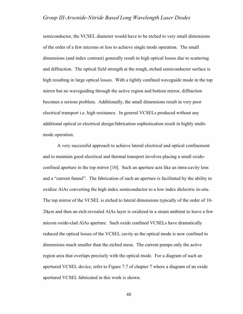
Group III-Arsenide-Nitride Based Long Wavelength Laser Diodes
semiconductor, the VCSEL diameter would have to be etched to very small dimensions
of the order of a few microns or less to achieve single mode operation. The small
dimensions (and index contrast) generally result in high optical losses due to scattering
and diffraction. The optical field strength at the rough, etched semiconductor surface is
high resulting in large optical losses. With a tightly confined waveguide mode in the top
mirror but no waveguiding through the active region and bottom mirror, diffraction
becomes a serious problem. Additionally, the small dimensions result in very poor
electrical transport i.e. high resistance. In general VCSELs produced without any
additional optical or electrical design/fabrication sophistication result in highly multi-
mode operation.
A very successful approach to achieve lateral electrical and optical confinement
and to maintain good electrical and thermal transport involves placing a small oxide-
confined aperture in the top mirror [10]. Such an aperture acts like an intra-cavity lens
and a “current funnel”. The fabrication of such an aperture is facilitated by the ability to
oxidize AlAs converting the high index semiconductor to a low index dielectric in-situ.
The top mirror of the VCSEL is etched to lateral dimensions typically of the order of 10-
20µm and then an etch-revealed AlAs layer is oxidized in a steam ambient to leave a few
micron oxide-clad AlAs aperture. Such oxide confined VCSELs have dramatically
reduced the optical losses of the VCSEL cavity as the optical mode is now confined to
dimensions much smaller than the etched mesa. The current pumps only the active
region area that overlaps precisely with the optical mode. For a diagram of such an
apertured VCSEL device, refer to Figure 7.7 of chapter 7 where a diagram of an oxide
apertured VCSEL fabricated in this work is shown.
48

Group III-Arsenide-Nitride Based Long Wavelength Laser Diodes
Chapter 4 Long Wavelength VCSELs
4.1 Long Wavelength VCSEL Issues
As was shown in the previous chapter, the VCSEL device is important because of
its low cost manufacturing potential. At the present time, tremendous success has been
achieved in the area of GaAs based VCSELs operating at approximately 850nm in terms
of performance and commercial application. Millions of 850nm VCSELs have been
deployed in commercial networking equipment, as they are the dominant laser source for
Gigabit Ethernet and Fibre Channel transceivers. However, as noted in chapter 2, longer
wavelengths at 1300nm and 1550nm have importance for higher bit-rate*distance
applications. Progress in developing long wavelength VCSELs has been relatively slow
due to inherent issues involved with the semiconductor materials used for long
wavelength edge emitters that preclude them for direct use in a VCSEL device.
Edge emitting laser diodes operating at 1300nm are made from InGaAsP based
materials grown on an InP substrate. Compared with the GaAs based materials, two big
differences exist that relate to VCSEL performance. First, the long wavelength InGaAsP
49

Group III-Arsenide-Nitride Based Long Wavelength Laser Diodes
lasers have inferior performance at high temperatures (lower T0) relative to shorter
wavelength GaAs lasers due to temperature sensitive absorption and carrier leakage (due
to the lower conduction band offsets). Secondly, the materials that can be grown lattice
matched on InP generally have low refractive index differences, making it very difficult
to fabricate high reflectivity DBR mirrors.
Because it is not possible to simply make devices analogous to GaAs based
VCSELs out of InP long wavelength materials several novel approaches are being
pursued to achieve long wavelength VCSELs. The approaches can be divided into three
general categories (i) those which are trying to develop better InP based mirrors (ii)
those that are trying to develop GaAs based long wavelength active regions and (iii) those
that try to integrate GaAs based mirrors with InP based active regions using novel
integration technology. The following sections will examine issues involved in all of
these approaches and will detail the logic behind the approach taken in this work.
4.2 DBR Mirror Issues
The DBR mirror has to support three general functions to be used in a VCSEL.
The mirror has to provide high reflectivity for the optical mode, provide a low resistance
current pathway for carrier injection into the active region, and efficiently transport heat
away from the active region to minimize the temperature rise of the active region.
4.2.1 Mirror Reflectivity
As detailed in the previous chapter, DBR mirrors achieve high reflectivity through
the coherent addition of many smaller reflections for multiple interfaces between
different materials. The strength of the reflection at each interface is related to the
50
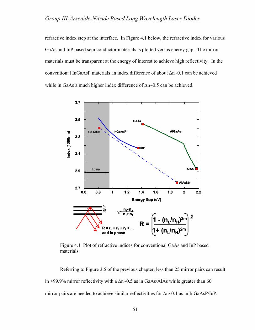
Group III-Arsenide-Nitride Based Long Wavelength Laser Diodes
refractive index step at the interface. In Figure 4.1 below, the refractive index for various
GaAs and InP based semiconductor materials is plotted versus energy gap. The mirror
materials must be transparent at the energy of interest to achieve high reflectivity. In the
conventional InGaAsP materials an index difference of about ∆n~0.1 can be achieved
while in GaAs a much higher index difference of ∆n~0.5 can be achieved.
2.7
2.9
3.1
3.3
3.5
3.7
0.6 0.8 1 1.2 1.4 1.6 1.8 2 2.2
InGaAsP AlGaAs
AlAsSb
GaAsSb
Lossy
InP
GaAs
AlAs
Energy Gap (eV)
Inde
x (1
300n
m)
2.7
2.9
3.1
3.3
3.5
3.7
0.6 0.8 1 1.2 1.4 1.6 1.8 2 2.2
InGaAsP AlGaAs
AlAsSb
GaAsSb
Lossy
InP
GaAs
AlAs
Energy Gap (eV)
Inde
x (1
300n
m)
n1n2n1
R = r1 + r2 + r3 + …add in phase
n1- n2rn= n1+ n2
n1n2n1
R = r1 + r2 + r3 + …add in phase
n1- n2rn= n1+ n2
n1- n2rn= n1+ n2
1 - (nL/nH)2m
1+ (nL/nH)2mR =
21 - (nL/nH)2m
1+ (nL/nH)2mR =
2
Figure 4.1 Plot of refractive indices for conventional GaAs and InP based materials.
Referring to Figure 3.5 of the previous chapter, less than 25 mirror pairs can result
in >99.9% mirror reflectivity with a ∆n~0.5 as in GaAs/AlAs while greater than 60
mirror pairs are needed to achieve similar reflectivities for ∆n~0.1 as in InGaAsP/InP.
51

Group III-Arsenide-Nitride Based Long Wavelength Laser Diodes
The large number of mirror pairs is problematic from the standpoints of optical loss,
electrical and thermal transport, and fabrication. With the low index contrast and >50
mirror pairs, light will penetrate deeply into the mirror (multiple microns to ten microns)
resulting in a large amount of diffraction and doping related optical loss. The thick
mirror is also more electrically resistive, leading to high levels of power
dissipation/heating. Because the InGaAsP materials have poor thermal conductivity
(detailed in the following section) the thermal impedance of the mirror is very poor.
Finally, growth of twice the device thickness results in impractically long growths and
excessive use of expensive source materials.
An alternative materials system for DBR mirrors on InP is the AlGaAsSb
materials system which can be grown on InP and has a high refractive index contrast
similar to GaAs/AlAs [11, 12, 13]. From an optical standpoint, the AsSb based mirror
approach is very effective. However, from a thermal standpoint the AsSb approach has
issues which will be described in the next section [14].
An alternative approach to mirror materials on InP is to use deposited dielectric
materials for one mirror [15]. The use of dielectric materials is problematic for both
mirrors as one mirror generally needs to be thermally conducting to remove dissipated
power. Dielectrics generally have very poor thermal conductivities. High index contrast
can be achieved with many of the widely used dielectric materials (Si/SiO2, CaF/ZnSe,
Al2O3/SiO2, etc). An issue often ignored in dielectrics is that optical loss can still play a
limiting role in the peak value of the reflectivity. The high index material of dielectric
mirrors is often really a deposited amorphous semiconductor which can have midgap
states that can absorb the laser light. For example, α-Si/SiO2 is widely available in
52

Group III-Arsenide-Nitride Based Long Wavelength Laser Diodes
semiconductor fabs and would be easy to incorporate in any laser fabrication procedure.
Because of the very large index contrast, ∆n~2.2, with α-Si/SiO2, a reflectivity of 99.5%
is achieved with only 3-4 mirror periods. However, α-Si has a loss coefficient of
approximately 300/cm which limits the peak reflectivity to about 99.5% no matter how
many more mirror periods are added.
Even if a dielectric material combination can be found that results in high index
contrast, good thermal conductivity, and low loss, a dielectric DBR approach is still
highly challenged because of the need to inject current around the mirror as opposed to
through the mirror. To achieve injection with a dielectric mirror, a contact has to formed
to a thin semiconductor layer that is within the VCSEL cavity. This layer has to be doped
heavily to minimize resistance, current crowding with non-uniform injection, and
parasitic heating which leads to significant optical loss dramatically reducing laser
performance.
4.2.2 Mirror Thermal Conductivity
In the VCSEL, at least one and preferably both mirrors need to have as high a
thermal conductivity as possible to conduct away active region heat and parasitic power
dissipated in the laser mirrors. This heat removal is crucial as the device heating can
enter a positive feedback loop or run away process where increasing active region
temperature results in higher current requirements which then further heat the active
region as illustrated in Figure 4.2.
53
Group III-Arsenide-Nitride Based Long Wavelength Laser Diodes
T goes up
Need more J
Jth=J0exp(T/T0) ∆T = Zth Pd ~ J* 1/σth
Figure 4.2 Illustration of problematic temperature-threshold current positive feedback loop.
For most geometries the thermal impedance of the mirror scales as 1/σ, where σ
is the thermal conductivity of the material. Plotted in Figure 4.3 is the thermal
conductivity of the relevant epitaxial material choices for DBR mirrors. As can be seen
the AlGaAs material system generally has and order of magnitude larger thermal
conductivity than the materials that can be grown on InP. The thermal conductivities for
the dielectric materials that result in high reflectivity DBR mirrors are essentially zero.
Another important phenomena shown in the figure is the poor thermal performance of
alloy materials due to alloy scattering of the heat carrying phonons. For the InP
compatible materials, an alloy must always be used except for InP itself, to achieve lattice
matching. In the case of GaAs based devices, pure AlAs and GaAs can be used to
achieve maximum thermal performance.
54

Group III-Arsenide-Nitride Based Long Wavelength Laser Diodes
0.01
0.1
1
0 0.2 0.4 0.6 0.8
AlxGa
1-xAs
on GaAs
AlxGa
1-xAsSb
on InP
GaxIn
1-xAsP
on InP
1
InP
Ther
mal
Con
duct
ivity
(W/c
m/K
)mole fraction x
0.01
0.1
1
0 0.2 0.4 0.6 0.8
AlxGa
1-xAs
on GaAs
AlxGa
1-xAsSb
on InP
GaxIn
1-xAsP
on InP
1
InP
Ther
mal
Con
duct
ivity
(W/c
m/K
)mole fraction x
Zth=∆T/Pd ~ 1/σth
N+ substrateN+ substrate
Heat flow
Thermal Conductivity of Mirror Materials
Figure 4.3 Thermal conductivities of semiconductor materials/alloys.
4.2.3 Mirror Approach Comparison
The lattice matched InGaAsP materials conventionally used on InP substrates
have poor refractive index contrast and result in low reflectivity, high diffraction and
absorption loss mirrors for VCSELs. From the preceding discussion, all long wavelength
VCSEL mirror approaches on InP that have resulted in high reflectivity mirrors on InP
(to date) employ materials that have very poor thermal conductivity. The epitaxial
materials that can be grown on InP generally are quaternary alloys that have poor thermal
conductivities due to alloy scattering of phonons. The dielectric materials that can be
deposited on InP that yield high reflectivity also have poor thermal conductivity. The
poor thermal conductivity of the VCSEL mirrors on InP make the temperature sensitive
InGaAsP active region have to operate at higher temperatures and result in very poor
laser performance.
55

Group III-Arsenide-Nitride Based Long Wavelength Laser Diodes
4.3 GaAs Based Long Wavelength Active Region Issues
Because of the challenges in making good VCSEL mirrors on InP substrates,
there is a large motivation to pursue achieving long wavelength VCSELs on GaAs
substrates. The high performance AlAs/GaAs DBR mirrors developed for 850nm and
980nm VCSELs could be employed and high performance lasers should result. The
missing component in long wavelength GaAs based devices is an active region that can
operate at >1µm in wavelength. As can been seen in the energy gap versus lattice
constant plot below, the longest wavelengths that can be achieved on GaAs employ
strained InGaAs. However, due to strain induced defect formation, the maximum amount
of indium which can be incorporated in thin quantum well structures is around 30%,
resulting in wavelengths around 1.1µm.
0
0.5
1
1.5
2
2.5
5.5 5.6 5.7 5.8 5.9 6 6.1 6.2
GaAs
AlAs
InAs
InxGa
1-xAs
AlxGa
1-xAs
InxAl
1-xAs
InP
980nm
1300nm
1550nm
InxGa
1-xAs
yP
1-y
Lattice Constant
Ener
gy G
ap
Energy Gap vs. Lattice Constant
Figure 4.4 Energy gap versus lattice constant for GaAs and InP based materials.
56

Group III-Arsenide-Nitride Based Long Wavelength Laser Diodes
The first long wavelength material grown on GaAs that was investigated was
InGaAs. The addition of indium to GaAs causes the bandgap to become smaller but it
also causes significant strain in the InGaAs layer. The large strain that develops because
of the larger size of indium results in two effects, the energy gap is altered and the layer
thickness becomes limited before defects are introduced. The strain is due to the
differences in the crystal structure when the larger InGaAs unit cell is forced to fit on the
smaller GaAs unit cell. Since the structure partially determines the electronic interaction
of the atoms of the lattice, the strain changes the band structure of the material. In the
case of InGaAs, the energy gap becomes larger due the strain effects.
Other approaches to achieve long wavelength active regions on GaAs include
InGaAs quantum dots[16], GaAsSb quantum wells [17, 18], and InGaAsN quantum wells
[19, 20]. In InGaAs quantum dots, a very high concentration of indium is grown in an
InGaAs layer under conditions that cause the spontaneous self assembly of pyramidal
20nm diameter islands or dots of high quality crystalline material. Because of the high
concentration of indium that can be incorporated in the quantum dots, emission at
1300nm has been observed [16]. Successful, low threshold edge emitting lasers have
been realized with the quantum dots but the low modal gain of the dots and the limited
active region thickness of VCSELs have limited quantum dot VCSELs to a few
experimental demonstrations that do not appear to very useful for high volume
manufacturing [21].
By adding antimony to GaAs quantum wells, the bandgap can be decreased and
1300nm emission has been observed. Like the quantum dot approach, the GaAsSb
approach also suffers from sensitivity to growth conditions because of the relative
57
Group III-Arsenide-Nitride Based Long Wavelength Laser Diodes
insolubility of antimony in GaAs and the potential for phase segregation. Successful
edge emitting and VCSEL devices have been fabricated after a tremendous amount of
work [22, 23], but like the InGaAs quantum dot lasers, few have been able to reproduce
the results.
Kondo is credited with discovering that the addition of nitrogen to (In)GaAs
layers results in a dramatic decrease in bandgap and can be suitable for long wavelength
laser diode fabrication [19, 24, 25]. This was somewhat counter-intuitive as group III-
nitrides have significantly wider bandgaps. The group III-nitrides, like the group III-
arsenides have good thermal performance, due in part to the large conduction band
offsets that result in good electron confinement in heterostructures. Because of their
good thermal performance and potential for long wavelength emission/gain, the group-
III-arsenide-nitrides appeared to be very well suited for the fabrication of long
wavelength VCSELs on GaAs substrates.
4.4 Alternate Approaches
In addition to the totally monolithic, wafer scale manufacturing compatible
approaches described above, several other approaches have been pursued to achieve long
wavelength VCSELs. The two most notable are wafer bonding and optical pumping.
In wafer bonding, several wafers are grown separately which each contain
different portions of the VCSEL [26, 27]. These different sections are combined together
after the growths. InP based wafers are employed for the active region with InGaAsP
quantum well active regions. For the mirrors, high performance GaAs based DBR
mirrors are used. In the first high temperature fusion process, one of the GaAs based
58
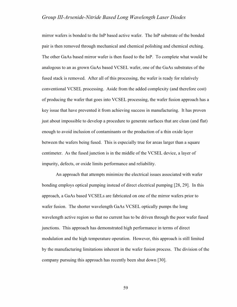
Group III-Arsenide-Nitride Based Long Wavelength Laser Diodes
mirror wafers is bonded to the InP based active wafer. The InP substrate of the bonded
pair is then removed through mechanical and chemical polishing and chemical etching.
The other GaAs based mirror wafer is then fused to the InP. To complete what would be
analogous to an as grown GaAs based VCSEL wafer, one of the GaAs substrates of the
fused stack is removed. After all of this processing, the wafer is ready for relatively
conventional VCSEL processing. Aside from the added complexity (and therefore cost)
of producing the wafer that goes into VCSEL processing, the wafer fusion approach has a
key issue that have prevented it from achieving success in manufacturing. It has proven
just about impossible to develop a procedure to generate surfaces that are clean (and flat)
enough to avoid inclusion of contaminants or the production of a thin oxide layer
between the wafers being fused. This is especially true for areas larger than a square
centimeter. As the fused junction is in the middle of the VCSEL device, a layer of
impurity, defects, or oxide limits performance and reliability.
An approach that attempts minimize the electrical issues associated with wafer
bonding employs optical pumping instead of direct electrical pumping [28, 29]. In this
approach, a GaAs based VCSELs are fabricated on one of the mirror wafers prior to
wafer fusion. The shorter wavelength GaAs VCSEL optically pumps the long
wavelength active region so that no current has to be driven through the poor wafer fused
junctions. This approach has demonstrated high performance in terms of direct
modulation and the high temperature operation. However, this approach is still limited
by the manufacturing limitations inherent in the wafer fusion process. The division of the
company pursuing this approach has recently been shut down [30].
59

Group III-Arsenide-Nitride Based Long Wavelength Laser Diodes
Chapter 5 Molecular Beam Epitaxy of
Group III-V-Nitrides
5.1 Molecular Beam Epitaxy
Molecular Beam Epitaxy, or MBE, is a physical vapor deposition technique
performed under ultra-high vacuum conditions which allows the growth of high quality
single crystal layers on top of a single crystal substrate. In the case of the III-V
compound semiconductors, beams of the crystal layer’s constituent atoms in the form of
atoms or molecules are generated by various means and are directed towards a heated
substrate where they react to form the crystal layer. The ultra-high vacuum ensures that
the atoms or molecules generated by the various sources travel in a controlled beam to
the substrate without interacting with each other or scattering off of other gas phase
species. Additionally, the ultra-high vacuum conditions minimize stray gas molecules
which could incorporate into the growing layer and compromise the layer purity.
60
Group III-Arsenide-Nitride Based Long Wavelength Laser Diodes
heated substrate
moleculesimpinging on
substrate
shutter
UHV: P~1E-10 Torrmean free path ~ 10m
heated ceramic crucible filled with source material to
produce “molecular beam”
heated substrate
moleculesimpinging on
substrate
shutter
UHV: P~1E-10 Torrmean free path ~ 10m
heated ceramic crucible filled with source material to
produce “molecular beam”
Figure 5.1 Diagram of MBE machine and crystalline layer growth process.
Most commonly the molecular beams are generated by the heating of solid
elemental source material to the point where vapor evaporates from a liquid (Ga, Al, In)
or sublimates from a solid (As, Sb, P, Si, Be). In the case of group III-V compound
semiconductor growth, the group III metals are solid at room temperature but melt to the
liquid phase at the temperatures needed to get a significant gas phase flux of atoms.
Arsenic remains a solid and sublimates as tetrameric arsenic, As4, at typical temperatures.
The tetrameric arsenic molecule can be converted to two dimeric arsenic molecules by
thermal cracking at a much higher temperature. Using cracked or dimeric arsenic is
preferable in many situations due to the higher incorporation efficiency and reactivity
relative to tetrameric arsenic. In this work cracked or dimeric arsenic was used
exclusively.
The growth of the crystalline layers occurs on a heated single crystal substrate.
The substrate provides a template for the growth of the other layers and therefore needs
to have a very similar crystal structure and lattice constant as the growing layers. The
61

Group III-Arsenide-Nitride Based Long Wavelength Laser Diodes
heat of the substrate provides enough thermal energy that atoms or molecules that stick to
the wafer can move around on and seek out the lowest energy bonding sites and then
overcome the potential barrier to react to form the crystal layer. These surface diffusion
processes are essential to the growth of high quality crystalline layers because the
generation of defects is generally less energetically favorable and the surface diffusion
allows the surface to come closer equilibrium. The heat of the substrate also causes many
impurities to desorb from the substrate surface and improves the layer purity.
In the work presented here, the substrate temperature was calibrated by
monitoring the changes in the surface reconstruction with temperature by Reflection High
Energy Electron Diffraction (RHEED). Several characteristic surface transitions occur in
the temperature range of 500-600ºC which can be used on every growth run to ensure
consistent growth temperatures. Below is example temperature data from two sequential
growth runs, demonstrating the need to monitor the temperature to yield consistent
temperatures.
62

Group III-Arsenide-Nitride Based Long Wavelength Laser Diodes
700
680
660
640
620
600
580
Ther
moc
oupl
e R
eadi
ng (C
)
580560540520Known Temperature (C)
Growth Run 1 Growth Run 2
Figure 5.2 Calibration of temperature of each growth run by comparing the thermocouple temperature at the surface phase transition which is known to occur at a particular temperature.
The group III-arsenide compound semiconductors are typically grown with a
substrate temperature in the range of 450-650ºC, which is low enough that the group III
metal atoms do not desorb from the surface. Arsenic can desorb from the substrate at
temperatures in this range so the flux of arsenic is generally considerably larger than that
of the metals. Flux ratios for arsenic flux relative to the total group III flux in the range
of 10-20:1 are commonly used and result in a large arsenic overpressure on the substrate
surface. Since the growth proceeds with an arsenic overpressure, the growth rate of the
layer is determined by the group III flux. Additionally, the composition of mixed group
III alloys is determined by the relative fluxes of the different group III constituents.
63

Group III-Arsenide-Nitride Based Long Wavelength Laser Diodes
5.2 Nitrogen Source Issues
5.2.1 Background
In order to grow nitrogen containing group III-V materials, a source of reactive
nitrogen needs to be available in the growth reactor being used. In MBE elemental
sources are commonly used to generate reactive fluxes of the constituent materials.
Elemental nitrogen occurs as a two nitrogen atom molecule which is a gas at room
temperature. However, the high strength of the bond between the two nitrogen atoms of
elemental nitrogen molecule, N2, makes elemental nitrogen essentially unreactive and not
usable for the growth of nitrogen containing group III-V materials by either MBE or
MOCVD. Typically, the group III-V materials and devices are grown by MBE or
MOCVD at temperatures in the range of 400-750ºC which is far too low to break the
elemental nitrogen bond on the surface of the wafer. For the growth of the wide bandgap
group III-Nitride materials, which occurs at the relatively high temperatures of 800-
1100ºC, the chemical nitrogen source ammonia, NH3, can be used in both MBE and
MOCVD [31]. The ammonia molecule is much more reactive than the nitrogen molecule
and can be decomposed in small but usable quantities on the surface of a hot wafer in the
presence of metal atoms (which serve to catalyze the decomposition of ammonia).
However, the growth of the group III-dilute nitride-arsenides generally needs to
be performed at much lower temperatures due to crystal quality issues. At temperatures
below 500ºC, which are typical for mixed arsenide-nitride materials, ammonia is
essentially unreactive. Other chemical sources of nitrogen which are more reactive than
nitrogen can be used, such as dimethylhydrazine. However, dimethylhydrazine is far
64

Group III-Arsenide-Nitride Based Long Wavelength Laser Diodes
from ideal because it is difficult to purify, highly toxic, and may react differently with the
different sources of the group III metals resulting in non-homogeneous epi-layers [32].
To avoid the difficulties of the chemical sources, a nitrogen plasma source can be used.
The strong bond of the elemental nitrogen can be broken by the highly energetic internal
conditions of an electromagnetically stimulated plasma. Under the appropriate plasma
conditions sufficiently large amounts of highly reactive atomic nitrogen can be obtained.
The major advantage of the plasma source approach is that the reactivity of the nitrogen
is independent of the substrate temperature which allows the separate optimization of the
nitrogen source reactivity and the substrate temperature (which has a strong effect on
crystal quality) [33].
For a radio-frequency (rf) plasma source, the most common plasma source used
for mixed nitride-arsenide materials, the variables affecting plasma operation are the rf
power that is coupled into the plasma and the pressure of the gas in the plasma chamber.
The rf power affects the plasma because it provides the energy to excite the nitrogen gas
molecules. The larger the rf power that is coupled into the plasma, the higher the degree
of excitation of individual gas species and the higher the fraction of the gas phase that is
excited. The down side of this is that energetic ions can be generated with can damage
the growing layer. The gas pressure is important because it determines the amount of
interaction the excited gas molecules/atoms have with other gas species. The lower the
gas pressure, the longer the time that gas species can interact with the electromagnetic
field without colliding with other gas molecules and possibly losing excitation. In order
to “ignite” the plasma a higher gas flow or gas pressure is required so that there is enough
excited species to be self-sustaining. After plasma ignition, the pressure or gas flow is
65
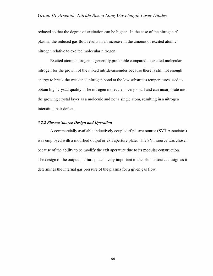
Group III-Arsenide-Nitride Based Long Wavelength Laser Diodes
reduced so that the degree of excitation can be higher. In the case of the nitrogen rf
plasma, the reduced gas flow results in an increase in the amount of excited atomic
nitrogen relative to excited molecular nitrogen.
Excited atomic nitrogen is generally preferable compared to excited molecular
nitrogen for the growth of the mixed nitride-arsenides because there is still not enough
energy to break the weakened nitrogen bond at the low substrates temperatures used to
obtain high crystal quality. The nitrogen molecule is very small and can incorporate into
the growing crystal layer as a molecule and not a single atom, resulting in a nitrogen
interstitial pair defect.
5.2.2 Plasma Source Design and Operation
A commercially available inductively coupled rf plasma source (SVT Associates)
was employed with a modified output or exit aperture plate. The SVT source was chosen
because of the ability to be modify the exit aperature due to its modular construction.
The design of the output aperture plate is very important to the plasma source design as it
determines the internal gas pressure of the plasma for a given gas flow.
66
Group III-Arsenide-Nitride Based Long Wavelength Laser Diodes
s
Broad molecular peaks
Figure 5.3 Emission Spectrum of Nitrgrowth. The sharper peaks at the longatomic nitrogen while the broad peaksnitrogren.
The plasma consists of excited electro
as they relax. The frequency or wavelength o
species. By measuring the plasma emission s
and gas flow, the trends in the relative concen
found. Figure 5.3 shows a plasma emission sp
amounts of atomic nitrogen compared to exci
the amount of “reactive nitrogen” versus rf po
nitrogen” refers to the total area under of the e
the sharp atomic nitrogen peaks. The amount
gas flow and with rf power. The gas flow ten
67
Sharp atomic peak
ogen r.f. plasma excitation used in MBE er wavelengths are due to transitions in at shorter wavelengths are due to molecular
ns, atoms, and molecules which emit light
f the light is very specific for each type of
pectrum while varying the plasma rf power
trations of the various excited species was
ectrum under conditions that result in large
ted molecular nitrogen. Figure 5.4 shows
wer and gas flow. The term “reactive
mission spectrum which is dominated by
of “reactive nitrogen” increases with both
ds to have a much weaker effect on the
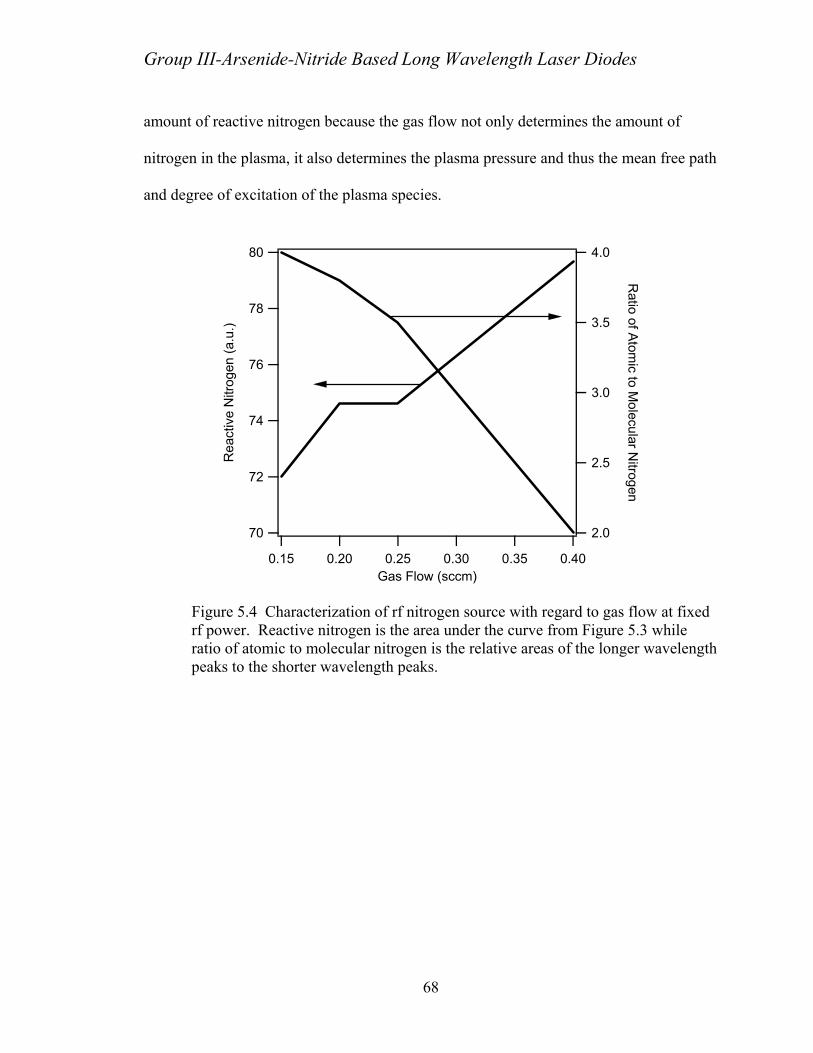
Group III-Arsenide-Nitride Based Long Wavelength Laser Diodes
amount of reactive nitrogen because the gas flow not only determines the amount of
nitrogen in the plasma, it also determines the plasma pressure and thus the mean free path
and degree of excitation of the plasma species.
80
78
76
74
72
70
Rea
ctiv
e N
itrog
en (a
.u.)
0.400.350.300.250.200.15Gas Flow (sccm)
4.0
3.5
3.0
2.5
2.0
Ratio of Atom
ic to Molecular N
itrogen
Figure 5.4 Characterization of rf nitrogen source with regard to gas flow at fixed rf power. Reactive nitrogen is the area under the curve from Figure 5.3 while ratio of atomic to molecular nitrogen is the relative areas of the longer wavelength peaks to the shorter wavelength peaks.
68

Group III-Arsenide-Nitride Based Long Wavelength Laser Diodes
80
75
70
65
60
55
50
Rea
ctiv
e N
itrog
en (a
.u.)
340320300280260r.f Power (Watts)
increasing gas flow
Figure 5.5 Characterization of rf nitrogen source with regard to rf power at two different gas flows.
The amount of atomic nitrogen relative to molecular nitrogen decreases with
increasing gas flow because the increased number of gas phase interactions/collisions at
higher flows or pressures which results in a lower degree of excitation. The relative
amount of atomic to molecular nitrogen increases with increasing rf power as would be
expected.
The general conditions developed for the nitrogen source operation consisted of
warming up the source by slowly ramping up the rf power over several minutes, igniting
the plasma with a moderate to large flow of gas, and finally reducing the gas flow to get
the plasma into a state of high excitation where there is large amounts of atomic nitrogen
relative to excited molecular nitrogen. The baseline nitrogen plasma source operating
conditions were 0.25sccm of N2 and 300W rf power.
69

Group III-Arsenide-Nitride Based Long Wavelength Laser Diodes
5.3 Growth Studies
The goal of the initial growth studies was to determine the appropriate conditions
to grow high quality GaNAs bulk layers. Growth of high quality layers is crucial to
achieve high performance laser devices. Major challenges in the growth of group III-
dilue nitride-arsenides are the large miscibility gap between InGaN and InGaAs and the
differences in crystal structure. Group III-Nitrides have a hexagonal crystal structure
while the group III-arsenides have a cubic crystal structure. The approach taken was to
use MBE, a non-equlibrium growth technique, to achieve the growth of metastable alloys
on GaAs substrates [34].
The high quality GaNAs bulk layers obtained from the optimized growth recipes
were used to determine properties such as lattice constant and energy gap. Finally, the
conditions to achieve high-quality GaNAs bulk layers served as a good starting place for
the development of high quality InGaNAs quantum wells.
5.3.1 GaNAs bulk growths
The challenge to growing high quality group III-nitride-arsenide materials is to
balance the need for high growth temperatures for purity and crystal quality with the need
for low temperatures to avoid phase segregation. It was found that if the substrate
temperature was below around 500ºC, good single crystal GaNAs layers could be grown,
while temperatures more typical of GaAs growth in the range of 600ºC resulted in phase
segregation and less overall nitrogen content [33]. Varying the operating conditions of
the plasma source significantly affected the plasma operation and output in a non-linear
manner. Both the amount of nitrogen atoms/molecules in the films and the relative
70

Group III-Arsenide-Nitride Based Long Wavelength Laser Diodes
amount of atomic to molecular nitrogen in the nitrogen beam and hence the crystal
quality, are controlled by the plasma operating mode. Once good operating condition
where achieve, they were kept constant for all growths and the nitrogen content of the
GaNAs layers was varied by changing the growth rate of the layer (the Ga flux). The
nitrogen content, with the plasma conditions fixed, was found to be very predictably
proportional to 1/growthrate, independent of temperature (as long as the temperature was
low <500ºC) implying that at the lower temperatures, the sticking coefficient of atomic
nitrogen is approximately one. Nitrogen mole fractions up to about 0.03 could be
obtained with relatively high quality.
2.8
2.6
2.4
2.2
2.0
1.8
1.6
Nitr
ogen
Per
cent
age
(%)
0.750.700.650.600.550.50growth rate (A/s)
Figure 5.6 Nitrogen composition vs growth rate at constant nitrogen source operation conditions. The linearity of the relationship indicates a constant incorporation rate (approximately unity) over the range of interest (1.5-3%).
With optimized growth conditions, high quality layers for the measurement of
lattice and bandgap were grown. Figure 5.7 shows examples of x-ray diffraction spectra
71
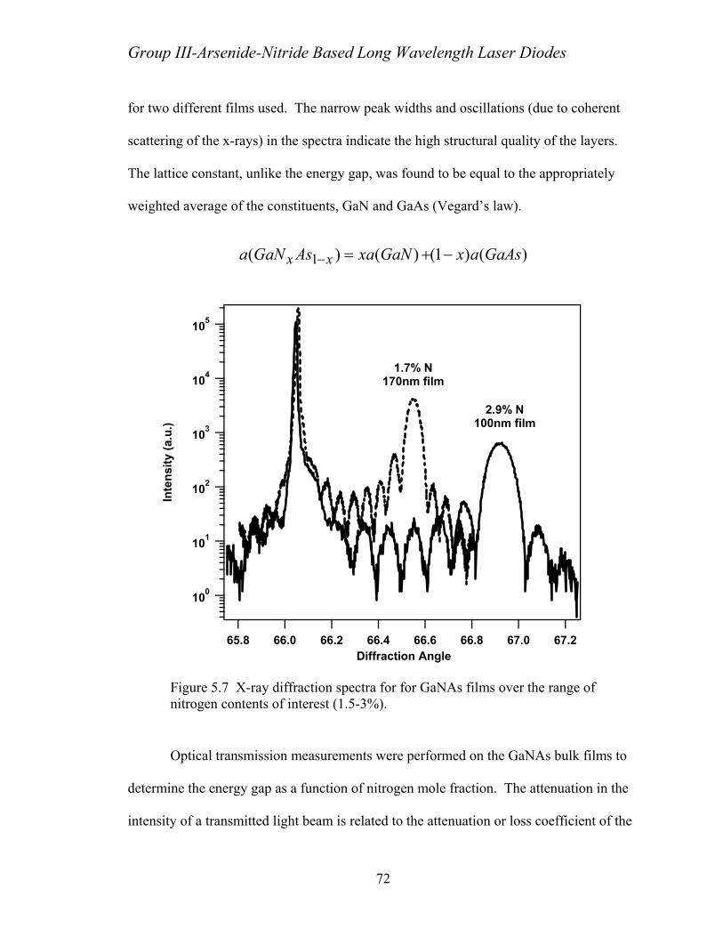
Group III-Arsenide-Nitride Based Long Wavelength Laser Diodes
for two different films used. The narrow peak widths and oscillations (due to coherent
scattering of the x-rays) in the spectra indicate the high structural quality of the layers.
The lattice constant, unlike the energy gap, was found to be equal to the appropriately
weighted average of the constituents, GaN and GaAs (Vegard’s law).
)()1()()( 1 GaAsaxGaNxaAsGaNa xx −+=−
100
101
102
103
104
105
Inte
nsity
(a.u
.)
67.267.066.866.666.466.266.065.8 Diffraction Angle
1.7% N170nm film
2.9% N100nm film
Figure 5.7 X-ray diffraction spectra for for GaNAs films over the range of nitrogen contents of interest (1.5-3%).
Optical transmission measurements were performed on the GaNAs bulk films to
determine the energy gap as a function of nitrogen mole fraction. The attenuation in the
intensity of a transmitted light beam is related to the attenuation or loss coefficient of the
72

Group III-Arsenide-Nitride Based Long Wavelength Laser Diodes
epi-layers and substrate, I=I0exp(-αL) where I is the optical intensity, α the absorption
coefficient and L the film thickness. In a simple model, at photon energies smaller than
the energy gap of a semiconductor the attenuation coefficient is zero and at photon
energies above the energy gap the attenuation for a direct gap bulk semiconductor should
be proportional to the square root of the photon energy. The square root dependence is
due to the functional form of the density of states. Plotting the square of the attenuation
coefficient extracted from optical transmission measurements versus the photon energy
should yield a straight line. Extrapolating back to zero attenuation should then yield the
value of the energy bandgap. Figure 5.8 shows an example of the procedure to extract
the attenuation coefficient as a function of photon energy for two GaNAs bulk films with
differing amounts of nitrogen.
73

Group III-Arsenide-Nitride Based Long Wavelength Laser Diodes
0.16
0.14
0.12
0.10
0.08
0.06
0.04
0.02
alph
a sq
uare
d
1.251.201.151.101.051.000.95Photon Energy (eV)
2.9% N 1.7% N
Figure 5.8 Plot of measured absorption coefficient squared. The linear relationship above the optical threshold is due to the direct bandgap of the Group III-Arsenide-Nitrides. Extrapolation to zero absorption yield the energy gap.
With the lattice constant and energy gap determined as a function of nitrogen
content, it is possible to make rough predictions as to the alloy compositions needed to
make long wavelength active regions. For example, to achieve 1.3µm emission, the
possible alloy compositions would be approximately In0.3Ga0.7N0.02As0.98 and
GaN0.05As0.95.
74
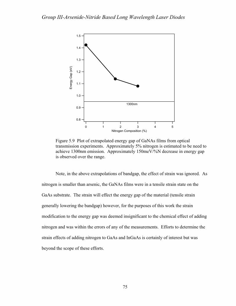
Group III-Arsenide-Nitride Based Long Wavelength Laser Diodes
1.5
1.4
1.3
1.2
1.1
1.0
0.9
0.8
Ene
rgy
Gap
(eV)
543210Nitrogen Composition (%)
1300nm
Figure 5.9 Plot of extrapolated energy gap of GaNAs films from optical transmission experiments. Approximately 5% nitrogen is estimated to be need to achieve 1300nm emission. Approximately 150meV/%N decrease in energy gap is observed over the range.
Note, in the above extrapolations of bandgap, the effect of strain was ignored. As
nitrogen is smaller than arsenic, the GaNAs films were in a tensile strain state on the
GaAs substrate. The strain will effect the energy gap of the material (tensile strain
generally lowering the bandgap) however, for the purposes of this work the strain
modification to the energy gap was deemed insignificant to the chemical effect of adding
nitrogen and was within the errors of any of the measurements. Efforts to determine the
strain effects of adding nitrogen to GaAs and InGaAs is certainly of interest but was
beyond the scope of these efforts.
75

Group III-Arsenide-Nitride Based Long Wavelength Laser Diodes
5.4 Quantum Well Development
Both In0.3Ga0.7N0.02As0.98 and GaN0.05As0.95 quantum well layers were grown with
GaAs barriers. The InGaNAs growth resulted in a specular wafer, while the GaNAs
growth resulted in a slightly foggy and rough wafer. Transmission Electron Microscopy
(TEM) was performed on the samples and is shown in Figure 5.10. Even at a higher
magnification, the InGaNAs well looks good with a sharp interface. The GaNAs well
looks very bad due to defects, possible phase segregation, and the strain fields around the
defects.
In0.30Ga 0.70N 0.02 As0.98 GaN0.05As0.95In0.30Ga 0.70N 0.02 As0.98 GaN0.05As0.95
Figure 5.10 TEM cross-sectional images of InGaNAs and GaNAs quantum well structures predicted to be capable of 1300nm light emission. Note, the InGaAsN MQW structure is shown at a higher magnification than that of the GaNAs
Because of the poor structural quality, GaNAs quantum wells were not pursued
further. In order to investigate the optical emission properties of the quantum well
samples, photoluminescence measurements were performed. Figure 5.11 shows the room
temperature photoluminescence from the InGaNAs multiple quantum wells. Also present
in the photoluminescence is the emission from InGaAs quantum wells grown on the same
76

Group III-Arsenide-Nitride Based Long Wavelength Laser Diodes
wafer that are identical to the InGaNAs wells except for the lack of nitrogen. The
measured samples consisted of N+ GaAs wafer with two 65Å InGaNAs quantum well
separated by 200Å GaAs barriers, a 500Å GaAs spacer layer, two 65Å InGaAs quantum
wells separated by 200Å GaAs barriers, and finally a 500Å GaAs capping layer. The
entire quantum well, barrier, spacer, and capping layers were grown at approximately
450ºC.
77
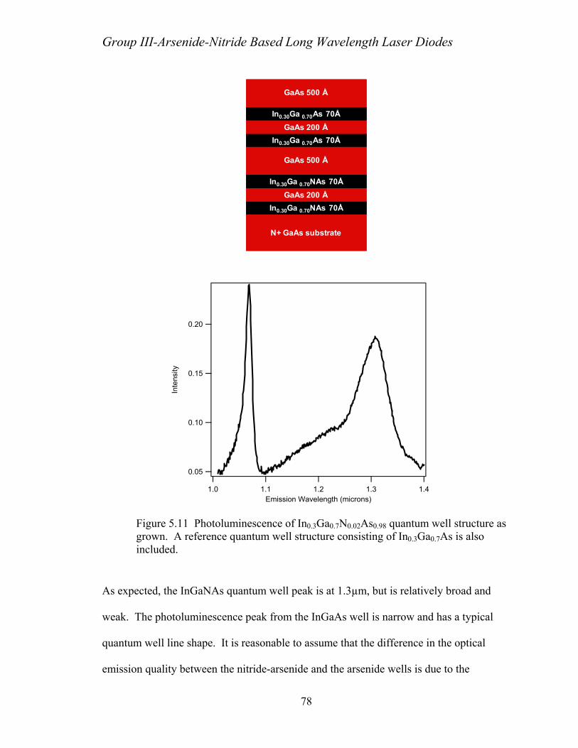
Group III-Arsenide-Nitride Based Long Wavelength Laser Diodes
In0.30Ga 0.70NAs 70Å
N+ GaAs substrate
In0.30Ga 0.70NAs 70ÅGaAs 200 Å
In0.30Ga 0.70As 70Å
GaAs 500 Å
In0.30Ga 0.70As 70ÅGaAs 200 Å
GaAs 500 Å
In0.30Ga 0.70NAs 70Å
N+ GaAs substrate
In0.30Ga 0.70NAs 70ÅGaAs 200 Å
In0.30Ga 0.70As 70Å
GaAs 500 Å
In0.30Ga 0.70As 70ÅGaAs 200 Å
GaAs 500 Å
0.20
0.15
0.10
0.05
Inte
nsity
1.41.31.21.11.0Emission Wavelength (microns)
Figure 5.11 Photoluminescence of In0.3Ga0.7N0.02As0.98 quantum well structure as grown. A reference quantum well structure consisting of In0.3Ga0.7As is also included.
As expected, the InGaNAs quantum well peak is at 1.3µm, but is relatively broad and
weak. The photoluminescence peak from the InGaAs well is narrow and has a typical
quantum well line shape. It is reasonable to assume that the difference in the optical
emission quality between the nitride-arsenide and the arsenide wells is due to the
78

Group III-Arsenide-Nitride Based Long Wavelength Laser Diodes
presence of nitrogen. To support this assumption further, samples with less nitrogen
were grown and characterized. Figure 5.12 shows the photoluminescence spectrum for a
sample with lower nitrogen, In0.3Ga0.7N0.01As0.99.
0.40
0.35
0.30
0.25
0.20
0.15
0.10
0.05
Inte
nsity
1.41.31.21.11.0Emission Wavelength (microns)
Figure 5.12 Photoluminescence of In0.3Ga0.7N0.01As0.99 quantum well structure as grown. A reference quantum well structure consisting of In0.3Ga0.7As is also included. Note the intensity axis is normalized to figure 5.9 above for comparison.
The lower nitrogen sample has a stronger and narrower photoluminescence peak at
shorter wavelengths indicating better crystal quality and a lower defect concentration
from the lower nitrogen content.
When the upper capping layer of the epi-structure was grown at a higher
temperature than the quantum well or other layers, it was observed that the emission
properties of the quantum wells were significantly altered. The photoluminescence peaks
79

Group III-Arsenide-Nitride Based Long Wavelength Laser Diodes
from the InGaNAs quantum wells increased dramatically in intensity and shifted to
shorter wavelengths. In parallel, other groups working on InGaNAs quantum wells
reported that post-growth annealing of the quantum well samples at high temperatures
resulted in improved emission properties with a blue shift in the peak wavelength [35].
Figure 5.13 shows photoluminescence spectra for quantum well samples that received
several different post-growth anneals.
1.0
0.8
0.6
0.4
0.2
Inte
nsity
(a.u
.)
1.41.31.21.11.0Emission Wavelength (microns)
as grown
RTA 775C 10s
600C in-situ during growth
Figure 5.13 Photoluminescence of In0.3Ga0.7N0.02As0.98 quantum well structures for varying amounts of annealing above the growth temperature. Note the intensity axis is normalized to figures above for comparison.
The peak photoluminescence intensity increases dramatically and the peak wavelength
shifts to shorter wavelengths (blue shifts). The increase in intensity is due to the
annealing process reducing the defect densities in the materials. There are several kinds
80

Group III-Arsenide-Nitride Based Long Wavelength Laser Diodes
of defects that are probably responsible for reducing the optical quality of the “as-grown”
samples. Since the samples are grown at low temperatures and a good bit of gas is
introduced with the plasma source operation, impurity concentrations could be
significantly elevated. The nitrogen source may also be so reactive that at low
temperatures, atomic nitrogen could also sit on the group III lattice sites or incorporate
into the growing layer as an interstitial. Also, molecular nitrogen could incorporate into
the growing layer either by sitting on a lattice site or by incorporating as an interstitial.
The nitrogen atom and molecule are both very small and could easily fit in an interstitial
or a lattice site (or a combination of the two in the case of the nitrogen molecule). The
annealing could reduce the density of any of these types of defects. For example,
annealing could cause an interstitial nitrogen atom or molecule to diffuse out from the
sensitive quantum well regions into surrounding material. The blue shift of the
photoluminescence should be due to either indium or nitrogen out diffusion from the
quantum wells increasing the bandgap of the quantum well and barrier materials [36].
5.5 Nitride-Arsenide MQW Growth Conclusion
This work has demonstrated that high optical quality InGaNAs multiple quantum
well structures can be grown by MBE using a rf plasma source for nitrogen. Important
parameters were the relatively low substrate growth temperature and the high arsenic
overpressures to avoid phase segregation. High temperature annealing of the grown
structure was found to be important in improving the optical emission performance,
likely removing as-grown defects. It is likely that the same far from thermodynamic
equilibrium growth conditions required to effectively combine such dissimilar materials
81
Group III-Arsenide-Nitride Based Long Wavelength Laser Diodes
as GaN and GaAs also permit crystal defects to be incorporated during growth. Post
(nitride-arsenide) growth annealing appears to effectively remove many of the as grown
defects.
82

Group III-Arsenide-Nitride Based Long Wavelength Laser Diodes
Chapter 6 Nitride Arsenide Edge
Emitting Lasers
6.1 Edge-Emitter Growth and Fabrication
After obtaining quantum well samples that had reasonable photoluminescence
intensities, edge-emitting laser diodes were fabricated to quantitatively assess the quality
of laser active regions based upon the same materials. The logic of spending a large
amount of effort studying edge emitting lasers, when the ultimate objective is to fabricate
VCSELs, is that the edge emitting device, due its simpler device structure, allows the
extraction or deconvolution of the active region performance from the measured device
performance. Additionally, even if the active regions are of only moderate to poor
quality, edge emitting laser operation is still often possible and useful data can be
extracted. Results from simple edge-emitter laser diodes were used to give good, rapid
feedback for the design of the next generation devices.
83
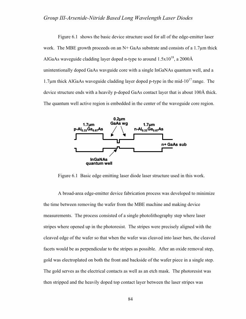
Group III-Arsenide-Nitride Based Long Wavelength Laser Diodes
Figure 6.1 shows the basic device structure used for all of the edge-emitter laser
work. The MBE growth proceeds on an N+ GaAs substrate and consists of a 1.7µm thick
AlGaAs waveguide cladding layer doped n-type to around 1.5x10¹⁸, a 2000Å
unintentionally doped GaAs wavguide core with a single InGaNAs quantum well, and a
1.7µm thick AlGaAs waveguide cladding layer doped p-type in the mid-1017 range. The
device structure ends with a heavily p-doped GaAs contact layer that is about 100Å thick.
The quantum well active region is embedded in the center of the waveguide core region.
1.7µmp-Al0.33Ga0.67As
1.7µmn-Al0.33Ga0.67As
InGaNAsquantum well
n+ GaAs sub
0.2µmGaAs wg1.7µm
p-Al0.33Ga0.67As1.7µm
n-Al0.33Ga0.67As
InGaNAsquantum well
n+ GaAs sub
0.2µmGaAs wg
Figure 6.1 Basic edge emitting laser diode laser structure used in this work.
A broad-area edge-emitter device fabrication process was developed to minimize
the time between removing the wafer from the MBE machine and making device
measurements. The process consisted of a single photolithography step where laser
stripes where opened up in the photoresist. The stripes were precisely aligned with the
cleaved edge of the wafer so that when the wafer was cleaved into laser bars, the cleaved
facets would be as perpendicular to the stripes as possible. After an oxide removal step,
gold was electroplated on both the front and backside of the wafer piece in a single step.
The gold serves as the electrical contacts as well as an etch mask. The photoresist was
then stripped and the heavily doped top contact layer between the laser stripes was
84

Group III-Arsenide-Nitride Based Long Wavelength Laser Diodes
removed by wet chemical etching from areas of the wafer which were not protected by
the gold. The wafer pieces are then cleaved into laser bars having lengths in the range of
600-1200µm.
There are several variables that can be altered to achieve that best performance
from a given active region. The growth temperature of the InGaNAs quantum wells has a
strong effect on device performance. Because the high growth temperatures used for the
growth of the upper waveguide cladding (AlGaAs) layers, the InGaNAs active region is
annealed in-situ. The growth time and temperature of these layers thus has an effect on
the active region performance. As was seen earlier with the annealing of quantum well
samples, the annealing of the active regions can have dramatic effects on performance.
Another very important variable is the nitrogen plasma ignition location during the
growth sequence. The plasma ignition procedure takes several minutes and causes a high
background of nitrogen gas in the MBE chamber for a few minutes. The nitrogen plasma
needs to be ignited prior to opening the nitrogen shutter and its usage in the active region.
6.2 Optimizing Growth Conditions
6.2.1 Initial growths
The first laser diode samples were grown with In0.3Ga0.7N0.01As0.99 single quantum
well active regions since these active regions yielded better photoluminescence than the
higher nitrogen content wells. The assumption was that the laser thresholds would be
lower for the quantum wells that had better photoluminescence. The 65Å quantum well
active region was grown at 450ºC and the upper waveguide cladding was grown at
580ºC. The growth temperature was ramped down to 450ºC during the growth of the
85

Group III-Arsenide-Nitride Based Long Wavelength Laser Diodes
first half of the GaAs waveguide core and the temperature was then ramped back up to
580ºC after the quantum well growth during the growth of the second half of the GaAs
waveguide core. The plasma was ignited during the growth of the last 1000Å of the Si
doped lower AlGaAs cladding layer.
After fabrication and cleaving into laser bars, the devices were tested at room
temperature under low duty cycle pulsed operation (<1µs pulses at 1% duty cycle). The
laser threshold currents were very high. For 20µm wide devices that were approximately
800µm in length, the threshold current densities were around 5-6kA/cm2. The laser
emission wavelengths were around 1.18µm, which was relatively consistent with the
wavelengths of the annealed quantum well samples.
Because the MBE system that the wafers were grown in was recently loaded and
had never produced laser diodes before, there was some concern that there might be some
problems with growing good laser diodes, let alone novel lasers based on nitride-arsenide
active regions. For example, there might be high oxygen or water levels in the MBE
chamber that results in poor lasers with AlGaAs in the structure. Also, the temperature
being used for the AlGaAs was on the low side of those normally used which could be
problematic as well. In order to verify the ability to make reasonable lasers in general,
InGaAs SQW laser diodes were grown and fabricated using the same design and growth
conditions as detailed above. The only change was the active region was now a single
80Å In0.22Ga0.88As quantum well grown at 490ºC. The laser thresholds for the 800µm
long laser diodes were about 300A/cm2, which is not record setting for such a laser
design, but it is certainly very reasonable for a non-optimized growth procedure.
86

Group III-Arsenide-Nitride Based Long Wavelength Laser Diodes
Since good InGaAs lasers could be grown with the MBE systems and the device
structure being used, the problem should have something to do with the plasma operation
and the low growth temperature of the quantum well and surrounding regions. Because
the photoluminescence from In0.3Ga0.7N0.01As0.99 quantum wells was at least as good as
that from InGaAs quantum wells, it was thought that the presence of nitrogen in the
quantum well might not be as much of an issue as how and where the plasma was ignited
during the growth sequence and how low the growth temperature was during the growth
of the quantum well and surrounding regions. To explore this idea, InGaAs SQW laser
diodes like those above were grown with the plasma ignited and operated as was done in
the InGaNAs laser diodes except that the nitrogen shutter remained closed during the
entire growth time. Additionally, InGaAs laser diodes were grown with the active and
surrounding regions grown at the same temperature as those layers in the InGaNAs laser
diodes (450ºC). The laser devices were characterized and both types of lasers
demonstrated approximately a factor of two increase in the threshold current density.
Therefore, both the low growth temperature and the plasma ignition and operation cause
a reduction in the quality of the active region. The low growth temperature most likely
allows more impurities to be incorporated as well as reducing the crystal quality. The
reason for the increase in threshold with the plasma merely operating with the shutter
always closed was investigated further through characterization of the poor quality
InGaNAs laser diodes.
6.2.2 Effect of Plasma lighting and operation
The location of the plasma ignition for the initial laser growths was chosen for
reasons of ease and simplicity. It takes some time to get the plasma running and
87
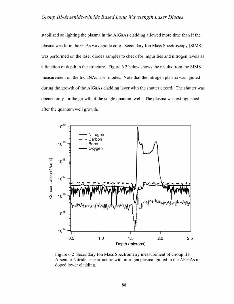
Group III-Arsenide-Nitride Based Long Wavelength Laser Diodes
stabilized so lighting the plasma in the AlGaAs cladding allowed more time than if the
plasma was lit in the GaAs waveguide core. Secondary Ion Mass Spectroscopy (SIMS)
was performed on the laser diodes samples to check for impurities and nitrogen levels as
a function of depth in the structure. Figure 6.2 below shows the results from the SIMS
measurement on the InGaNAs laser diodes. Note that the nitrogen plasma was ignited
during the growth of the AlGaAs cladding layer with the shutter closed. The shutter was
opened only for the growth of the single quantum well. The plasma was extinguished
after the quantum well growth.
1014
1015
1016
1017
1018
1019
1020
Con
cent
ratio
n (1
/cm
3)
2.52.01.51.00.5Depth (microns)
Nitrogen Carbon Boron Oxygen
Figure 6.2 Secondary Ion Mass Spectrometry measurement of Group III-Arsenide-Nitride laser structure with nitrogen plasma ignited in the AlGaAs n-doped lower cladding.
88

Group III-Arsenide-Nitride Based Long Wavelength Laser Diodes
The most significant result of the SIMS measurement is that the nitrogen
concentration in the epi-layers is large, even when the shutter is closed. The nitrogen
level spikes when there is the large gas flow needed for the plasma ignition procedure,
then drops as the gas flow is reduced. The nitrogen level increases in the GaAs layer
because of the slower GaAs growth rate used compared to the AlGaAs layer. The
nitrogen content then spikes to a large value for the quantum well as expected. The
quantum well nitrogen concentration profile is not very precise because of depth
resolution limitations of the SIMS measurement. The nitrogen levels then drops to the
background level when the plasma is extinguished. The high nitrogen levels with the
shutter closed were fairly surprising because there is no direct line of sight from the
plasma source to the substrate with the shutter closed. Nonetheless, there are high levels
of nitrogen in materials when the nitrogen shutter is closed.
Also of note in the SIMS profile are the low levels of oxygen, carbon, and boron.
Oxygen is know to result in very efficient optical emission suppressing deep levels in
GaAs materials (especially those containing aluminum). The SIMS of the laser structures
indicates oxygen levels low enough that they would not be expected to inhibit laser
performance. Carbon is expected to be a major contaminant in a recently serviced and
loaded MBE system. Boron-Nitride is the material from which the active chamber of the
nitrogen plasma source is fabricated. It is possible that the energetic plasma could cause
the BN to degrade releasing boron into the active nitrogen molecular beam. Both carbon
and boron levels were found to be low, demonstrating the efficacy of the MBE system
preparation (bake out and sacrificial growths).
89

Group III-Arsenide-Nitride Based Long Wavelength Laser Diodes
Laser diodes with the plasma ignited during the growth of the GaAs waveguide
core were next grown, fabricated, and tested. The laser diodes showed laser thresholds
about one half of those with the plasma ignited during the growth of the AlGaAs cladding
layers. The threshold current densities were about 2-3kA/cm2 with a wavelength of about
1.18µm. The conclusion that can be drawn is that having reactive nitrogen in the
chamber during the growth of AlGaAs is very detrimental to laser performance. There
are two likely effects of the nitrogen being present in the AlGaAs. First, the nitrogen
may reduce the crystal quality of the AlGaAs because of very strong bond between
Aluminum and Nitrogen and because AlN has a different crystal structure than GaAs.
Additionally, there is some evidence that a small amount of nitrogen or other impurities
in AlGaAs can cause the ability to dope the materials n-type to be lost. If the n-type
doping of the AlGaAs is lost, the location of the depletion region of the diode under
forward bias could be in the AlGaAs region and not the active region. The injection of
carriers would be mostly into this AlGaAs region which is defected due to the nitrogen
incorporation and low growth temperature.
Igniting the plasma during the growth of the GaAs is better because the
incorporation of nitrogen into GaAs is lower and the GaAs layers are not intentionally
doped. Also, GaAsN can be grown with relatively high structural quality, as was shown
in chapter 4.
6.2.3 Optimizing the growth temperature of the active region and cladding layers
With the large decrease in laser threshold currents that was obtained by lighting
the plasma on the GaAs waveguide core while the GaAs was grown at high temperature,
90

Group III-Arsenide-Nitride Based Long Wavelength Laser Diodes
the next part of the growth sequence was to optimize was the growth temperatures of the
active region and upper waveguide cladding layers.
In an attempt to get longer wavelength laser diodes, the amount of nitrogen in the
quantum well of the active region was increased form 1.2% to 2%. Because the
photoluminescence from wells with 2% nitrogen was worse that than of the 1.2%
nitrogen wells, the thresholds of the laser diodes were expected to be significantly worse.
However, the laser thresholds were found to be dramatically better. The threshold
current density for 20µm x 800µm SQW edge-emitters was about 1.1kA/cm2 with an
emission wavelength of 1.25µm. This threshold current is about a factor of two lower
than that of the lower nitrogen content lasers, despite having worse as-grown
photoluminescence. However, comparing the photoluminescence from the laser diodes
themselves, the higher nitrogen content lasers do have stronger emission intensity than
the lower nitrogen content lasers.
In order to get the higher nitrogen content in the active region while keeping the
plasma content the same, the overall growth rates had to be decreased. Therefore, the
growth of the AlGaAs cladding layer that anneals the active region in-situ took much
longer to grow for the higher nitrogen content lasers compared to the lower nitrogen
content lasers. The difference in the amount of annealing therefore explains why the
higher nitrogen content lasers with worse as-grown photoluminescence could have lower
threshold currents. To further verify this hypothesis, the lower nitrogen content laser
samples were annealed ex-situ in a rapid thermal annealer and the photoluminescence
was measured. The emission intensity increased to at least the level of the higher
nitrogen content lasers.
91

Group III-Arsenide-Nitride Based Long Wavelength Laser Diodes
Another line of evidence that showed the importance of the thermal cycling of the
active region had to do with temperature uniformity of the growths. The substrate heater
and the substrate holders used in the MBE system resulted in large temperature non-
uniformities across the wafer at high temperatures. For the low temperature growth of
the active regions, the temperature was relatively constant across the wafer. However, at
the high temperatures used for the growth of the GaAs and AlGaAs portions of the laser
diodes, the temperature non-uniformity was large. The temperature of the wafer is
coldest in the center and increases dramatically with radius. Photoluminescence maps of
the laser wafers showed much stronger emission intensity from the hotter edge portions
of the wafer. Figure 6.3 shows an example of a plot of intensity (at a fixed wavelength)
versus radius for a laser wafer. The excitation source was the 6328Å line from a HeNe
laser. The dramatic increase in intensity with radius is due to the increase in growth
temperature of the AlGaAs cladding with radius due to the non-uniformity of the
holders/heater. The higher temperatures at the outer portions of the wafer reduce the as-
grown defect densities and improve the emission properties dramatically.
92
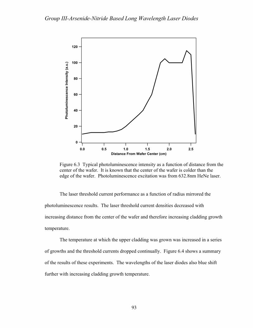
Group III-Arsenide-Nitride Based Long Wavelength Laser Diodes
120
100
80
60
40
20
0
Phot
olum
ines
cenc
e In
tens
ity (a
.u.)
2.52.01.51.00.50.0Distance From Wafer Center (cm)
Figure 6.3 Typical photoluminescence intensity as a function of distance from the center of the wafer. It is known that the center of the wafer is colder than the edge of the wafer. Photoluminescence excitation was from 632.8nm HeNe laser.
The laser threshold current performance as a function of radius mirrored the
photoluminescence results. The laser threshold current densities decreased with
increasing distance from the center of the wafer and therefore increasing cladding growth
temperature.
The temperature at which the upper cladding was grown was increased in a series
of growths and the threshold currents dropped continually. Figure 6.4 shows a summary
of the results of these experiments. The wavelengths of the laser diodes also blue shift
further with increasing cladding growth temperature.
93

Group III-Arsenide-Nitride Based Long Wavelength Laser Diodes
2500
2000
1500
1000
500
0
Thre
shol
d (A
/cm
2)
660640620600580Cladding Growth Temperature (C)
1.26
1.25
1.24
1.23
1.22
Laser Wavelength (m
icrons) Threshold Wavelength
Figure 6.4 Laser upper cladding growth temperature study. As noted, the growth of the upper cladding anneals the active structure. Data from 20x800um broad area laser diodes.
The laser diode performance is also very sensitive to the growth temperature of the active
region. In a series of growths in the range of 400-500ºC, the temperature of 440ºC was
found to be optimum. Both above and below this temperature, the laser thresholds
increased dramatically. Above approximately 460ºC the wafer was not specular,
indicating some type of phase segregation or major crystal quality issue. It appears that
the optimum growth temperature for the active region is as hot as possible before
crystalline degradation mechanisms (likely phase segregation) become limiting.
94
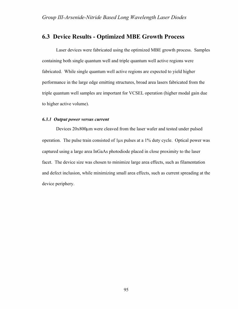
Group III-Arsenide-Nitride Based Long Wavelength Laser Diodes
6.3 Device Results - Optimized MBE Growth Process
Laser devices were fabricated using the optimized MBE growth process. Samples
containing both single quantum well and triple quantum well active regions were
fabricated. While single quantum well active regions are expected to yield higher
performance in the large edge emitting structures, broad area lasers fabricated from the
triple quantum well samples are important for VCSEL operation (higher modal gain due
to higher active volume).
6.3.1 Output power versus current
Devices 20x800µm were cleaved from the laser wafer and tested under pulsed
operation. The pulse train consisted of 1µs pulses at a 1% duty cycle. Optical power was
captured using a large area InGaAs photodiode placed in close proximity to the laser
facet. The device size was chosen to minimize large area effects, such as filamentation
and defect inclusion, while minimizing small area effects, such as current spreading at the
device periphery.
95

Group III-Arsenide-Nitride Based Long Wavelength Laser Diodes
40
30
20
10
0
Opt
ical
Pow
er (m
w)
0
)
Inte
nsity
(a.u
.)
Figure 6.5 Light-quantum well edgwith 1µs pulses at
(a
35030025020015010050Current (mA)
1220
)
Curre em 1%
(b
125012451240123512301225Wavelength (nm)
ent relationship (a) and emission spectrum (b) of single itting laser diode. Devices were tested in pulsed operation duty cycle. Device size was 20x800µm.
96
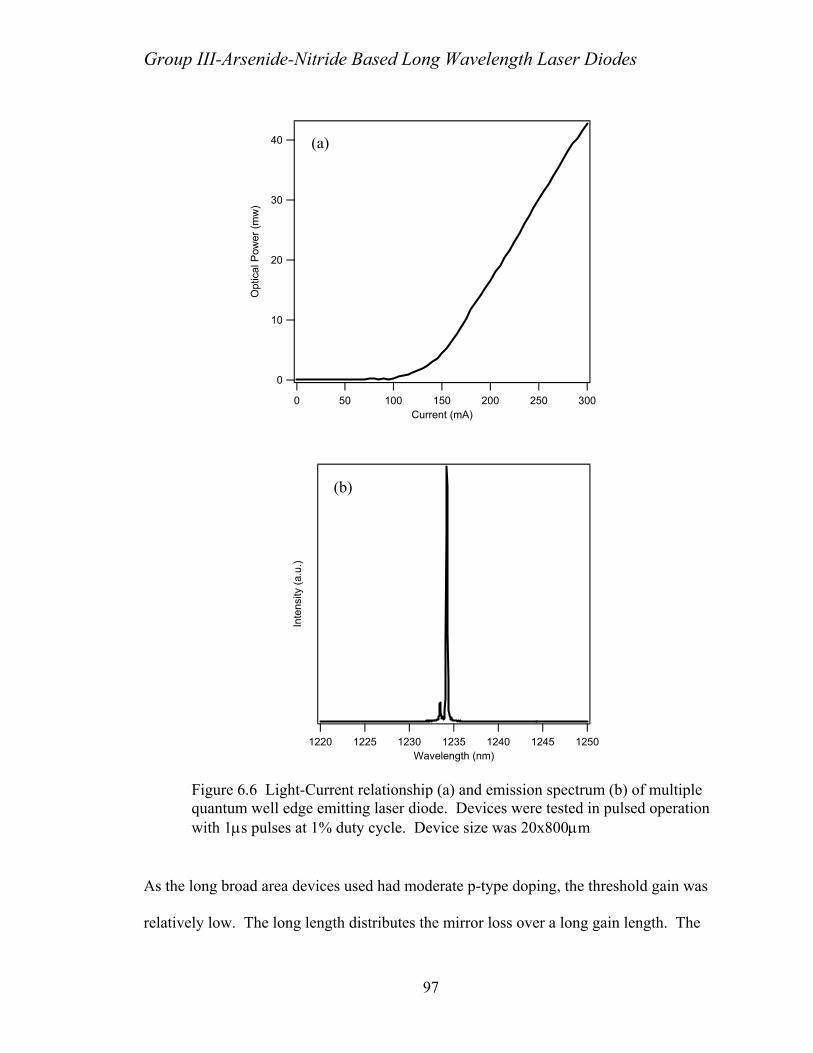
Group III-Arsenide-Nitride Based Long Wavelength Laser Diodes
40
30
20
10
0
Opt
ical
Pow
er (m
w)
0
Inte
nsity
(a.u
.)
Figure 6.6 Light-quantum well edgwith 1µs pulses at
As the long broad area de
relatively low. The long
(a)
30025020015010050Current (mA)
122
Cure em 1%
vic
len
(b)
1250124512401235123012250Wavelength (nm)
rent relationship (a) and emission spectrum (b) of multiple itting laser diode. Devices were tested in pulsed operation
duty cycle. Device size was 20x800µm
es used had moderate p-type doping, the threshold gain was
gth distributes the mirror loss over a long gain length. The
97

Group III-Arsenide-Nitride Based Long Wavelength Laser Diodes
low to moderate p-doping was used to keep the distributed loss (that not due to the active
structure) low. Because of the relatively low threshold gain, the single quantum well
samples always had lower threshold currents as they could always yield sufficient gain to
lase. However, the multiple quantum well laser diodes exhibited lower threshold current
density per quantum well. The threshold current density of 20µmx800µm size devices
was 450A/cm2 for single quantum well variants and 600A/cm2 for triple quantum well
variants.
6.3.2 Thermal performance
Laser device performance was measured as a function of heatsink temperature.
The current pulses supplied to the lasers was short enough that self heating was
minimized. One of the major motivating factors of a GaAs based long wavelength active
region is the anticipated good high temperature performance. High temperature
performance is crucial for practical VCSEL operation as VCSELs are nearly always
deployed in optical transceivers which do not supply cooling to maintain device
temperature near room temperature. The typical required operating temperature range is
–5ºC to +85ºC. Note, that due to voltage drop associated with the DBR mirrors, VCSELs
typically have ~10ºC of self heating in addition to the ambient temperature.
98
Group III-Arsenide-Nitride Based Long Wavelength Laser Diodes
190
180
170
160
150
140
130
120
Thre
shol
d (m
A)
350340330320310300Temperature (K)
T0 ~140K
Ith=I0exp(T/T0)
Figure 6.7 Laser threshold current as a function of stage temperature. Triple quantum well device was tested in pulsed operation with 1µs pulses at 1% duty cycle. Device size was 20x800µm. A high characteristic temperature of 140K was extrapolated.
99

Group III-Arsenide-Nitride Based Long Wavelength Laser Diodes
1255
1250
1245
1240
Wav
elen
gth
(nm
)
8070605040Temperature (°C)
~0.4nm/°C
Figure 6.8 Laser emission wavelength as a function of stage temperature. Device was tested in pulsed operation with 1µs pulses at 1% duty cycle. Device size was 20x800µm. The wavelength shift with temperature is very typical of semiconductor laser diodes due to shift of gain spectrum with temperature.
The previous results are crucial to demonstrating the viability of the InGaAsN
quantum well active region. The high T0 and the demonstrated operation at >80ºC
indicate that the active region when incorporated in a VCSEL structure should be capable
of CW performance over the needed operating range for commercial viability. The upper
limit on the high temperature operation in the previous experiments was not the devices,
it was the temperature stage used which was only rated to 70ºC. The T0 value is
consistent with other GaAs laser devices with similar conduction band offsets. If
AlGaAs barriers are employed either in the quantum well structure or as barriers around
the active region to keep carriers from being injected into the doped waveguide regions as
minority carriers, higher values of T0 are expected.
100

Group III-Arsenide-Nitride Based Long Wavelength Laser Diodes
6.4 Edge-Emitter Laser Conclusions
The simple edge emitting laser platform developed enabled the improvement of
the InGaNAs quantum well active region beyond that of the photoluminescence
experiments detailed in chapter 5. Through optimization of the plasma ignition
procedure and location in the device layer structure, the active region growth
temperature, and post growth anneal temperature of the active region InGaNAs laser
diodes operating in the range of 1.22-1.25µm with threshold current densities within a
factor of 1.5 of similar InGaAs quantum well lasers operating at 0.97µm. The thresholds
of the longer wavelength lasers are expected to be higher than those with shorter
wavelength emission due to the higher optical absorption losses at the longer
wavelengths. The active regions were also shown to be quite immune to temperature
increases relative to InP based long wavelength active regions as demonstrated by the
high T0 of 140K. The high performance and low temperature sensitivity optical emission
properties of the InGaNAs active structures will be of great utility in successful, practical
VCSEL device operation.
101

Group III-Arsenide-Nitride Based Long Wavelength Laser Diodes
Chapter 7 Group III-Arsenide-Nitride
VCSELs
7.1 Large Area VCSELs
Broad or large area VCSELs were fabricated using a very simple fabrication
procedure to test the VCSEL epi-material prior to attempting to make small area VCSELs
to potentially operate continuous wave.
7.1.1 Device design and Fabrication
VCSEL devices were designed with ease of growth and fabrication in mind. The
output mirror of a VCSEL typically is around 99.5% reflecting while the other mirror is
as high a reflectivity as possible (~99.9%). In order to achieve these high reflectivities,
22-30 mirror pairs are required. A substrate emitting design is possible because the GaAs
substrate is transparent at wavelengths longer than about 0.9µm. A substrate emitting
device has several advantages compared to a top emitting device. In a bottom emitting
102

Group III-Arsenide-Nitride Based Long Wavelength Laser Diodes
device, the growth time is minimized because a metallic reflector can be deposited on top
of the top mirror, enhancing the top mirror reflectivity. To achieve a given reflectivity,
fewer semiconductor layers are needed because the metallic reflector adds to the overall
reflectivity. With fewer semiconductor layers, the growth time is minimized, which is of
great practical importance (to be discussed below). The use of fewer semiconductor
layers is also important in the top p-type mirror because of the resistance associated with
the p-type layers and the heterojunctions between the mirror materials. Because the
deposited metal on the top mirror is continuous without the need for an emission window,
the metal can also serve as a heat spreader, helping to remove the heat generated in the
resistive top mirror. In contrast, a top emitting device must have many more mirror
layers and can only have a small ring contact which is not very effective for heat
removal.
The minimization of the growth time is important for several reasons. Because of
the large thickness of the device and the low growth rates, the growth time is on the order
of 24 hours. The growth rates are low because the amount of active nitrogen flux from
the plasma source and the limited number of cells in the MBE system. With large growth
times, source drift can be appreciable which can cause errors in layer thickness. Growth
errors can translate into poor device performance because of increased optical loss and
improper cavity mode wavelength. Additionally, large growth times are problematic
because the high growth temperatures used to grow (Al)GaAs can cause thermally
induced changes in temperature sensitive layers or quantum wells. For example, dopants
such as Be have a high diffusivity at high temperature and the designed doping profile
can be altered due to thermal diffusion. Also, as discussed in the previous chapters, the
103

Group III-Arsenide-Nitride Based Long Wavelength Laser Diodes
emission properties of InGaNAs quantum wells seem to be sensitive to amount of time at
high temperature.
Figure 7.1 below is a schematic diagram of the device design employed. A three
quantum well active region similar to that used in the edge emitters of the previous
chapter is employed. The GaAs cavity has doping offsets of 50nm for the Be p-type and
Si n-type dopants. The bottom mirror consists of 22.5 pairs of GaAs and AlAs quarter
wave layers with abrupt heterojunctions. The bottom mirror contains uniform n-type Si
dopants at a level of 1x10¹⁸/cm3 for the first half of the mirror near the cavity and
2x10¹⁸/cm3 for the last half further away from the cavity. The upper mirror consists of 22
pairs of GaAs and AlAs quarter wave layers. The heterojunctions were parabolically
graded over a distance of 10nm. The Be p-type dopant was kept at a level of 5x10¹⁷/cm3
in the fields of the first half of the mirror and was increased to a level of 1x10¹⁸/cm3 for
the second half of the mirror (which was also grown at a lower temperature). The dopant
level increases on the wide bandgap side and of the graded heterojunction region to
minimize the series resistance of each heterointerface in the top mirror. A Ti/Au layer on
top serves as both the top electrical contact and a reflector to enhance the overall
reflectivity of the composite mirror. The top GaAs layer thickness was chosen to
properly phase match the reflection from the gold layer (with its complex refractive
index) with the reflections from the other layers of the DBR.
Square metal pads varying in diameter from 10µm to 100µm were patterned by
conventional photolithography. Wet etching with sulfuric acid, hydrogen peroxide, and
water mixture was used to etch a mesa into the top p-type mirror using the metal pad as
an etch mask.
104

Group III-Arsenide-Nitride Based Long Wavelength Laser Diodes
N+ GaAs substrate
Ti:Au reflector and top contact
20 pair p-AlAs/p-GaAs DBRparabolic grading at interfaces
22 pair n-AlAs/n-GaAs DBRabrupt interfaces
3 InGaNAs/GaAs 70Å/200Å active region
λ cavity
Substrate emission
Figure 7.1 VCSEL device structure used in this work.
7.1.2 Device Reflectivity Characterization
Reflectivity measurements were made both during the growth and on the final
epi-structure. The growth was performed in several steps so that the reflectivity data
could be used to correct for inaccuracies in the growth rate calibration and drift in the
sources. After a reflectivity measurement was made, the intended device structure was
varied in computer simulation tools to attempt to match the measured spectrum. As the
growth times were known precisely and the actual growth rates could be determined very
precisely. For example, during the VCSEL growth, the first 5 mirror pairs of the bottom
mirror were grown and the reflectivity was measured and then simulated. The mirror
center wavelength will be off of that intended due to non-repeatability in the MBE
sources. However, they are not off enough that the VCSEL device performance will
suffer once the rest of the mirror layers are grown correctly after the in-situ reflectivity
correction. The reflectivity of the VCSEL structure was also measured after the growth
the active region and 95% of the laser optical cavity. In the VCSEL device it is crucial to
105

Group III-Arsenide-Nitride Based Long Wavelength Laser Diodes
align the cavity mode or resonance to the mirror center wavelength and the gain spectrum
of the quantum well active region. The mirror center wavelength is easily seen in the
mirror reflectivity data. The gain spectrum location can often be inferred from the
reflectivity data due to the presence of excitonic absorption that can be observed slightly
below the band edge absorption. The band edge absorption increases gradually and is
difficult to observe, however the excitonic absorption typically is abrupt and has several
features associated with the heavy and light hole masses which are split by the quantum
well.
Figure 7.2 below shows the reflectivity spectrum of the completed InGaNAs
VCSEL device near the center of the completed wafer. The center and cavity mode
wavelength is shorter than the 1220-1250nm of the edge emitter devices because the
exitonic absorption was (anticipated and) observed to be shifted shorter due to the long
growth time which anneals the active region.
0
0.2
0.4
0.6
0.8
1
1050 1100 1150 1200 1250 1300 1350
Fabry-Perot1212 nm
Wavelength (nm)
Figure 7.2 In-situ reflectivity spectrum of VCSEL wafer just after completion of growth. Measurement was performed a few millimeters off of center.
106
Group III-Arsenide-Nitride Based Long Wavelength Laser Diodes
Reflectivity measurements performed at various radii, shown in Figure 7.3 below,
were also performed and revealed a feature of the MBE growth system used. The
temperature non-uniformity was large enough to cause a variation of the center
wavelength by about 100nm across the wafer. The center of the wafer was cooler while
the edges were hotter. The upper half of the laser cavity and the top mirror were grown
at high temperatures to avoid any oxygen contamination issues in the aluminum
containing materials as well as to anneal the InGaNAs active region. The growth
temperature was hot enough that gallium had a non-zero evaporation rate from the wafer
so that the temperature non-uniformity resulted in a GaAs layer thickness variation across
the wafer. As the cavity mode shifted blue from center to edge of the wafer, the top
mirror reflectivity also decreased because of the mismatch of the GaAs and AlAs layers
from a quarter wave of the cavity mode wavelength. Additionally, as the optical
emission performance of the InGaNAs active region is known to generally increase with
the amount of annealing the active region performance was anticipated to be the best
towards the edge of the wafer. Putting all these effects together, it was expected that the
best device performance would be observed off of center where the best compromise
between mirror loss and active region performance was achieved. The test results in the
next section bore out this expectation.
107
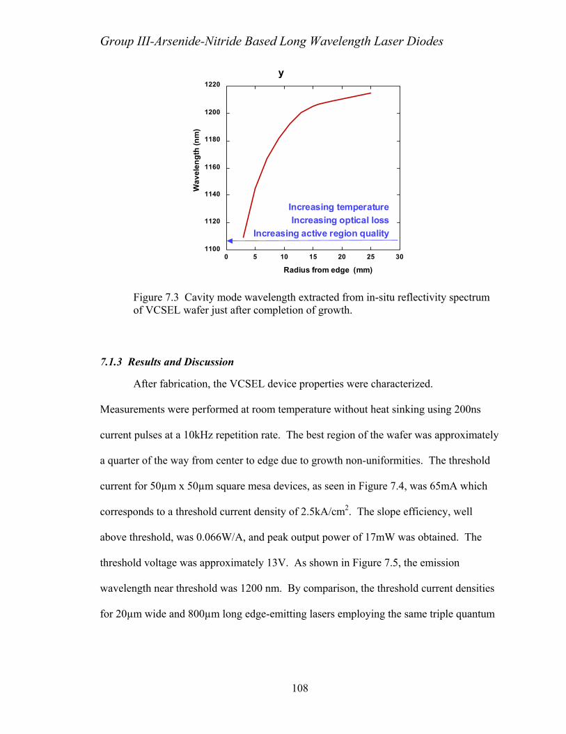
Group III-Arsenide-Nitride Based Long Wavelength Laser Diodes
1100
1120
1140
1160
1180
1200
1220
0 5 10 15 20 25 30
y
Radius from edge (mm)
Wav
elen
gth
(nm
)Increasing temperatureIncreasing optical loss
Increasing active region quality
Figure 7.3 Cavity mode wavelength extracted from in-situ reflectivity spectrum of VCSEL wafer just after completion of growth.
7.1.3 Results and Discussion
After fabrication, the VCSEL device properties were characterized.
Measurements were performed at room temperature without heat sinking using 200ns
current pulses at a 10kHz repetition rate. The best region of the wafer was approximately
a quarter of the way from center to edge due to growth non-uniformities. The threshold
current for 50µm x 50µm square mesa devices, as seen in Figure 7.4, was 65mA which
corresponds to a threshold current density of 2.5kA/cm2. The slope efficiency, well
above threshold, was 0.066W/A, and peak output power of 17mW was obtained. The
threshold voltage was approximately 13V. As shown in Figure 7.5, the emission
wavelength near threshold was 1200 nm. By comparison, the threshold current densities
for 20µm wide and 800µm long edge-emitting lasers employing the same triple quantum
108

Group III-Arsenide-Nitride Based Long Wavelength Laser Diodes
well active region were as low as 600A/cm2 and edge-emitters lased at wavelengths of
1235-1250nm.
0
4
8
12
16
20
0 100 200 300 400 500
Output powerVoltage
Out
put P
ower
(mW
), Vo
ltage
(V)
Current (mA)
Figure 7.4 Light output power and voltage against injection current (L-I-V) characteristics at room temperature for a InGaNAs VCSEL; inset shows details of threshold region.
109
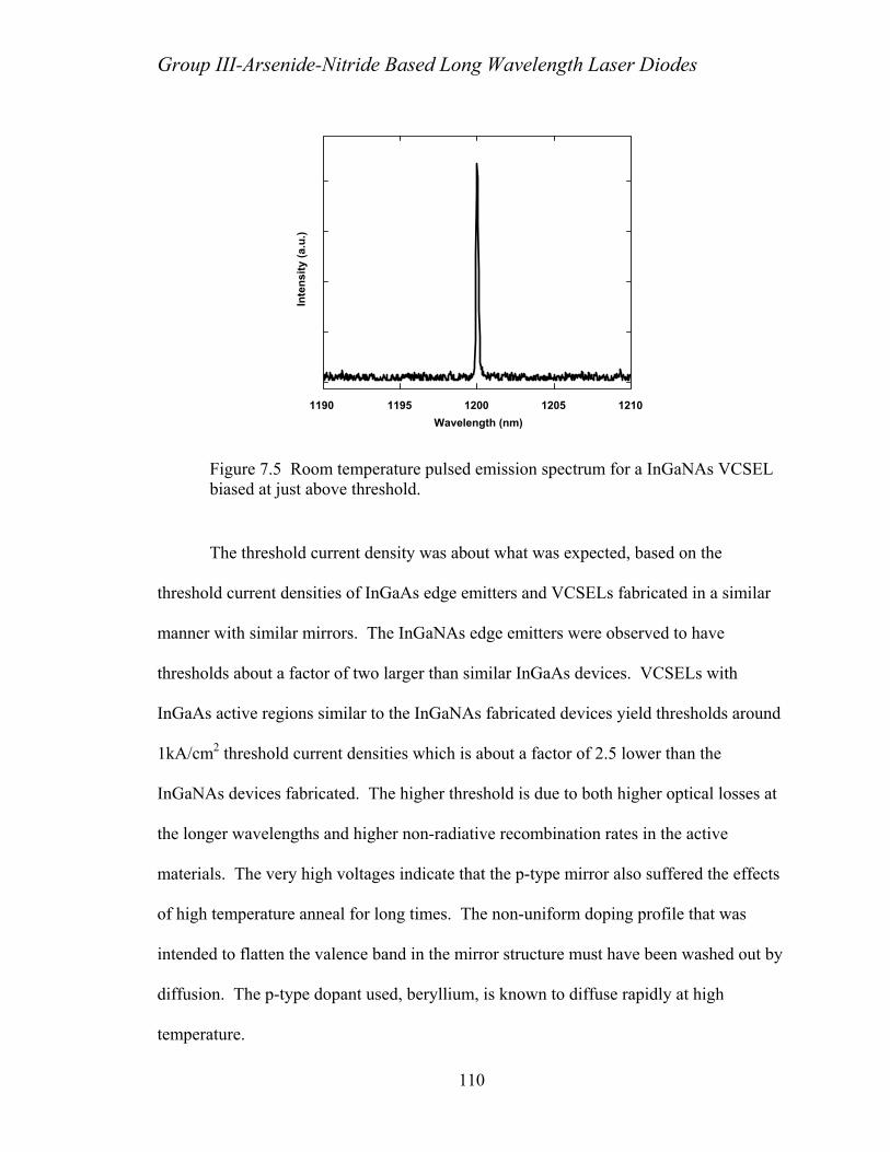
Group III-Arsenide-Nitride Based Long Wavelength Laser Diodes
1190 1195 1200 1205 1210
Inte
nsity
(a.u
.)
Wavelength (nm)
Figure 7.5 Room temperature pulsed emission spectrum for a InGaNAs VCSEL biased at just above threshold.
The threshold current density was about what was expected, based on the
threshold current densities of InGaAs edge emitters and VCSELs fabricated in a similar
manner with similar mirrors. The InGaNAs edge emitters were observed to have
thresholds about a factor of two larger than similar InGaAs devices. VCSELs with
InGaAs active regions similar to the InGaNAs fabricated devices yield thresholds around
1kA/cm2 threshold current densities which is about a factor of 2.5 lower than the
InGaNAs devices fabricated. The higher threshold is due to both higher optical losses at
the longer wavelengths and higher non-radiative recombination rates in the active
materials. The very high voltages indicate that the p-type mirror also suffered the effects
of high temperature anneal for long times. The non-uniform doping profile that was
intended to flatten the valence band in the mirror structure must have been washed out by
diffusion. The p-type dopant used, beryllium, is known to diffuse rapidly at high
temperature.
110
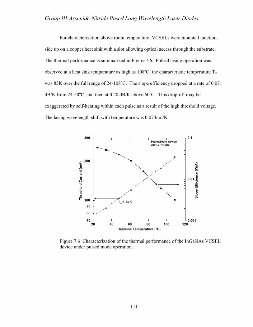
Group III-Arsenide-Nitride Based Long Wavelength Laser Diodes
For characterization above room temperature, VCSELs were mounted junction-
side up on a copper heat sink with a slot allowing optical access through the substrate.
The thermal performance is summarized in Figure 7.6. Pulsed lasing operation was
observed at a heat sink temperature as high as 108ºC; the characteristic temperature T0
was 85K over the full range of 24-108˚C. The slope efficiency dropped at a rate of 0.071
dB/K from 24-50ºC, and then at 0.20 dB/K above 60ºC. This drop-off may be
exaggerated by self-heating within each pulse as a result of the high threshold voltage.
The lasing wavelength shift with temperature was 0.074nm/K.
70
80
90
100
200
300
0.001
0.01
0.1
20 40 60 80 100 120
Thre
shol
d C
urre
nt (m
A)
Slop
e Ef
ficie
ncy
(W/A
)
Heatsink Temperature (°C)
T0 = 85 K
50µmx50µm device200ns / 10kHz
Figure 7.6 Characterization of the thermal performance of the InGaNAs VCSEL device under pulsed mode operation.
111

Group III-Arsenide-Nitride Based Long Wavelength Laser Diodes
7.2 CW VCSEL Devices
In order to achieve CW operation, the power dissipation and associated heating of
the active region must be reduced significantly. Additionally, reducing the threshold gain
requirement by reducing the optical loss would aid substantially. Both objectives were
met by exploiting the ability to oxidize AlAs to form an electrical and optical aperature,
confining both current and light to smaller dimensions than that of the etched structure.
The reduced optical losses and smaller active volume reduced the threshold current of the
VCSEL device substantially. Additionally, the large etched structure with the small
active region results in a lower electrical resistance and a lower device thermal
impedance by helping to remove heat from the active region.
7.2.1 Device Structure
The CW InGaNAs VCSEL device structure is shown schematically in Figure 7.7
below, and consists of the InGaNAs multiple-quantum-well (MQW) active region placed
within the VCSEL cavity surrounded by the top and bottom mirrors. The bottom mirror is
a 22.5 period n-doped GaAs–AlAs distributed Bragg reflector (DBR) designed for a
center wavelength near 1200nm. Centered within the GaAs cavity, which forms a p-i-n
diode, is an active region of three 70Å InGaNAs quantum wells separated by 200Å GaAs
barriers. The top mirror is a 20 period p-doped GaAs–AlAs DBR, on top of which is
grown an additional p-type contact layer whose 630Å thickness is chosen to appropriately
allow the reflection from the overlying 40Å Ti/1200Å Au contact electrode to add in
phase with the DBR. The AlAs layers of the lowest three mirror periods of the top mirror
were used to form the oxide aperture during the selective lateral oxidation process. Since
112
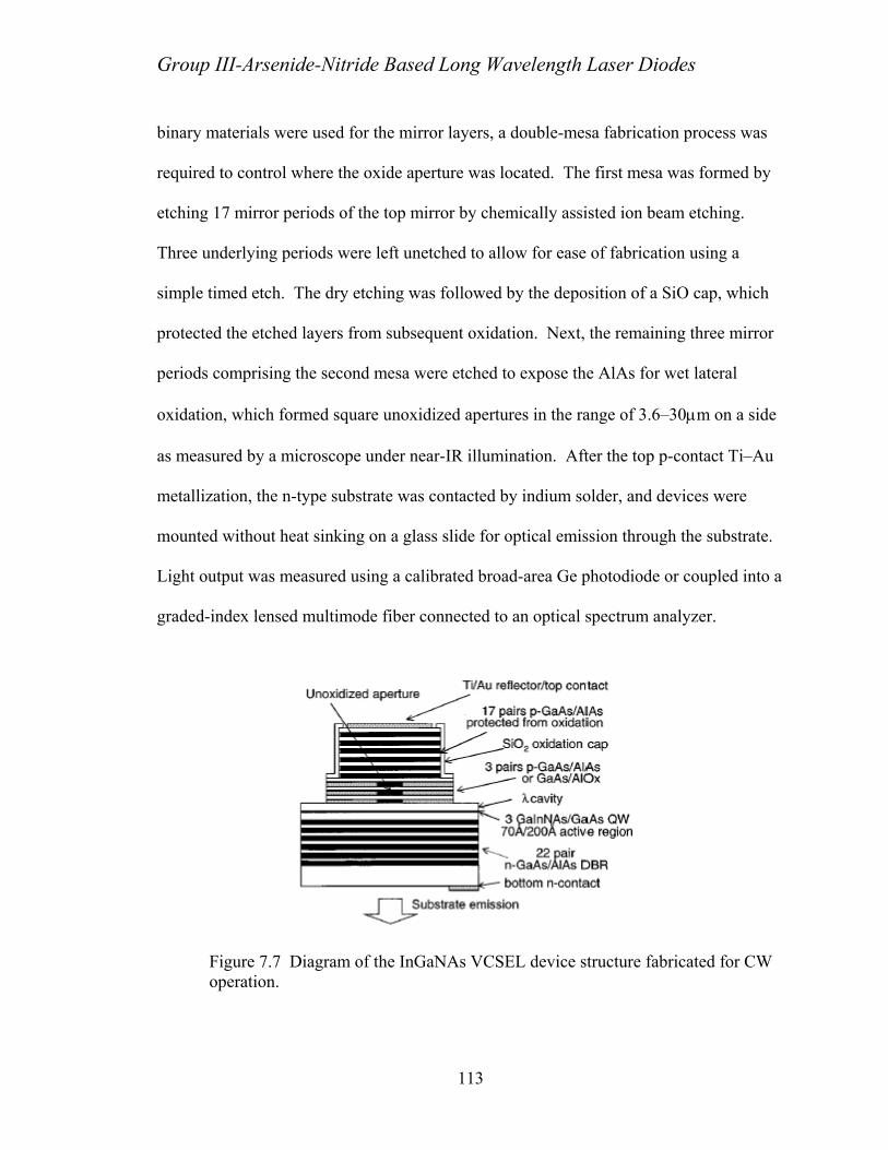
Group III-Arsenide-Nitride Based Long Wavelength Laser Diodes
binary materials were used for the mirror layers, a double-mesa fabrication process was
required to control where the oxide aperture was located. The first mesa was formed by
etching 17 mirror periods of the top mirror by chemically assisted ion beam etching.
Three underlying periods were left unetched to allow for ease of fabrication using a
simple timed etch. The dry etching was followed by the deposition of a SiO cap, which
protected the etched layers from subsequent oxidation. Next, the remaining three mirror
periods comprising the second mesa were etched to expose the AlAs for wet lateral
oxidation, which formed square unoxidized apertures in the range of 3.6–30µm on a side
as measured by a microscope under near-IR illumination. After the top p-contact Ti–Au
metallization, the n-type substrate was contacted by indium solder, and devices were
mounted without heat sinking on a glass slide for optical emission through the substrate.
Light output was measured using a calibrated broad-area Ge photodiode or coupled into a
graded-index lensed multimode fiber connected to an optical spectrum analyzer.
Figure 7.7 Diagram of the InGaNAs VCSEL device structure fabricated for CW operation.
113
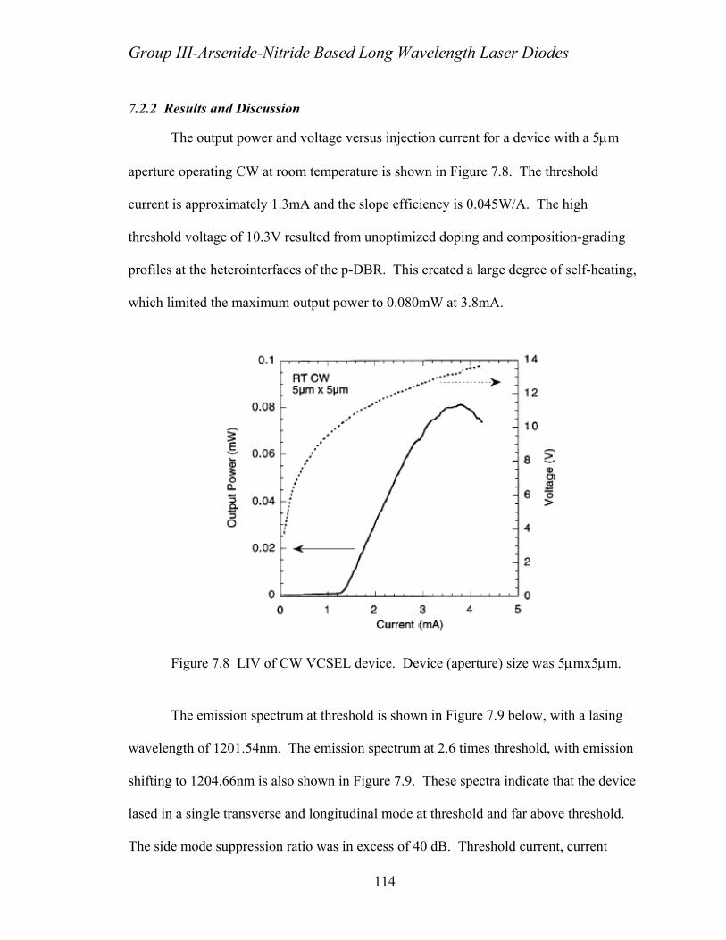
Group III-Arsenide-Nitride Based Long Wavelength Laser Diodes
7.2.2 Results and Discussion
The output power and voltage versus injection current for a device with a 5µm
aperture operating CW at room temperature is shown in Figure 7.8. The threshold
current is approximately 1.3mA and the slope efficiency is 0.045W/A. The high
threshold voltage of 10.3V resulted from unoptimized doping and composition-grading
profiles at the heterointerfaces of the p-DBR. This created a large degree of self-heating,
which limited the maximum output power to 0.080mW at 3.8mA.
Figure 7.8 LIV of CW VCSEL device. Device (aperture) size was 5µmx5µm.
The emission spectrum at threshold is shown in Figure 7.9 below, with a lasing
wavelength of 1201.54nm. The emission spectrum at 2.6 times threshold, with emission
shifting to 1204.66nm is also shown in Figure 7.9. These spectra indicate that the device
lased in a single transverse and longitudinal mode at threshold and far above threshold.
The side mode suppression ratio was in excess of 40 dB. Threshold current, current
114

Group III-Arsenide-Nitride Based Long Wavelength Laser Diodes
density, and slope efficiency as a function of device size are summarized in Figure 7.10.
Solid marks correspond to CW operation, unfilled ones are pulsed operation.
Figure 7.9 Emission spectra of CW InGaNAs VCSEL device at threshold (1.3mA) and far above threshold (3.5mA). The wavelength shift is consistent with the temperature rise with the increased drive current. Single mode operation is obtained with an SMSR >40dB.
The VCSEL wavelength shifted with dissipated power at a rate of 0.092nm/mW.
As the wavelength shift with temperature obtained from broad-area pulsed VCSELs was
0.074nm/K (detailed earlier), a temperature rise of approximately 60K above ambient
temperature at peak output power and a thermal impedance of 1.24K/mW is estimated.
The fact that CW operation was possible for these VCSEL devices in spite of the large
excess power dissipation is indicative of the low temperature sensitivity of the InGaNAs
MQW active region, coupled with the relatively high thermal conductivity of GaAs-based
binary materials. CW laser operation also occurred for device sizes ranging from 3.6µm
115

Group III-Arsenide-Nitride Based Long Wavelength Laser Diodes
to 6.4µm, with threshold currents from 0.94mA to 2.3mA and slope efficiency as high as
0.049W/A.
Figure 7.10 Threshold current, threshold current density, and slope efficiency as a function of device size. Solid symbols are for CW operation while open symbols are for pulsed operation.
Devices were also tested under pulsed operation to probe device characteristics as
a function of aperture size independent of thermal effects. Figure 7.11 shows the typical
output power and voltage as a function of pulsed injection current (200ns at 10kHz) for
several device sizes. Threshold current, current density, and slope efficiency versus
aperture size are summarized for a wider range of devices in Figure 7.10. Pulsed
threshold current varied from 0.89mA for 3.6µm devices to approximately 21mA for
29µm sizes. Threshold current density was within the range of 2–2.5 kA/cm2 at larger
116

Group III-Arsenide-Nitride Based Long Wavelength Laser Diodes
sizes, and slope efficiency above 0.09W/A was achieved. Slope efficiency dropped for
aperture sizes below 7µm, which was likely due to optical scattering, and current density
rose to nearly 7kA/cm2 for the smallest (3.6µm) devices. The increase in threshold with
decreasing aperture size was not attributed to an increase in surface recombination as the
active region was unetched and the oxidized aperture was a reasonable distance from the
active region. Optimization of the oxide aperture thickness, shape, and placement with
respect to the optical standing wave should also reduce this excess scattering for small
devices in a similar fashion as it has for near-IR VCSELs [10]. Characteristics of
VCSELs operating CW are also included in Figure 7.10. Under CW operation, efficiency
fell by approximately 30% compared to pulsed mode due to self heating, accompanied by
a slight increase in threshold current. This behavior is consistent with previous reports on
pulsed etched-pillar devices at high temperature [5, 14], where the temperature sensitivity
of the slope efficiency was more pronounced than that of the threshold current. One
possible explanation is temperature-dependent absorption in the DBRs combined with
gain/cavity-mode detuning effects.
117

Group III-Arsenide-Nitride Based Long Wavelength Laser Diodes
Figure 7.11 Light output power and voltage versus injection current under pulsed operation for InGaNAs VCSELs with varying aperture sizes.
7.3 VCSEL Conclusions
In summary, large area InGaNAs multiple quantum well VCSELs were
demonstrated that emit at 1.2µm and are capable of pulsed operation over the temperature
range of 24-108ºC. These large-area devices exhibit a threshold current density as low as
2.5kA/cm2 and a characteristic temperature of 85K.
Low-threshold InGaNAs VCSELs operating CW at room temperature were also
demonstrated. Devices exhibited milliamp threshold currents and peak output powers
above 0.08mW. Future improvements in performance should be readily achieved by
further adapting well-established 850nm VCSEL technology. Higher output power will
be possible by reducing the resistance of the p-DBR through better control of
composition grading and doping, and lower threshold current by reducing scattering in
118

Group III-Arsenide-Nitride Based Long Wavelength Laser Diodes
small-aperture devices. High-temperature performance will be improved through reduced
self-heating. Finally, 1300nm emission should be achieved by increasing the indium
and/or nitrogen content of the InGaNAs–GaAs MQW active layer.
119

Group III-Arsenide-Nitride Based Long Wavelength Laser Diodes
Chapter 8 Summary and Future
Directions
8.1 Summary of Accomplishments
Presented below is a simple “bullet-ized” list of the technical accomplishments of
the work presented in this dissertation.
• A molecular beam epitaxy system employing a custom nitrogen rf plasma
source was developed specifically for the growth of group III-Arsenide-Dilute
Nitrides on GaAs substrates.
• Through extensive growth and materials characterization experiments growth
conditions were developed that resulted in high quality InGaAsN crystal layers
that emit light in the range of 1.22-1.26µm.
• Edge emitting lasers based on the InGaNaAs were fabricated that exhibited
record low threshold current densities at laser wavelengths >1.22µm due the
high crystalline quality associated with the developed growth processes.
120

Group III-Arsenide-Nitride Based Long Wavelength Laser Diodes
• Edge emitting lasers demonstrated excellent potential for uncooled operation
and high power due to the measured temperature sensitivity of the active region.
The characteristic temperature,T0, was measured to be 140K, similar to GaAs
lasers and much higher than conventional InP based long wavelength active
structures.
• Large area vertical cavity lasers were demonstrated that yielded operation at
temperatures exceeding 109ºC.
• Oxide confined InGaNAs VCSELs were developed that demonstrated
continuous wave operation at room temperature with ultra-low threshold
currents.
8.2 Future Directions
There are several lines of work that naturally follow from the work performed in
this dissertation. There is a large amount of device fabrication and characterization that
remains to be done, even for the active regions as they were developed in this work. Due
to the commercial importance of these devices, there will not likely be a lack of work in
these areas. The most important work for the mixed arsenide-nitride materials to
progress to commercial viability is to explore in detail the materials, defect, and
fundamental reliability physics of the InGaNAs materials. As demonstrated in earlier
chapters, the mixed nitride-arsenide materials must be grown at relatively low
temperatures to avoid phase segregation and major crystal defects. However, the low
growth temperature also results in the incorporation of significant point defect densities
which require annealing to eliminate and stabilize. Investigation of the crystal growth
mechanisms and alternate means than low temperature to stabilize the growing layer
could be very important. As shown in chapter 6, InGaAs lasers grown at similarly low
121

Group III-Arsenide-Nitride Based Long Wavelength Laser Diodes
temperatures also demonstrated poor performance. Such low temperature InGaAs
devices were able to recover some of their performance through annealing, but never
attained the full performance of their counter-parts grown at higher temperatures,
indicating that some defects that are incorporated at low temperatures can not be fully
removed by annealing. While requiring annealing to reduce and stabilize the defect
density may be quite practical as a device fabrication process and sufficient performance
may be achieved despite not achieving the full performance potential, it does cause
concern for device reliability as initial point defect densities are generally a source of
long term failure in laser diodes. Studies need to be performed on the long term stability
of the InGaNAs materials. It is fortunate that a large amount of study has been devoted
to the reliability of InGaAs lasers as they are used in pump lasers in erbium doped fiber
amplifiers where high reliability is essential. Approaches similar to InGaAs laser studies
need to be employed where high temperature, current, and optical power are used to
accelerate the failure modes of the laser devices.
This thesis has clearly demonstrated the potential to realize low cost long
wavelength VCSELs based on InGaNAs active regions combined with the extensive
design and manufacturing foundation of 850nm VCSELs. If the remaining materials and
reliability issues are addressed, practical deployment is surely not far behind.
122
Group III-Arsenide-Nitride Based Long Wavelength Laser Diodes
Chapter 9 References
9.1 Cited References
1 G.P. Agrawal, Fiber-Optic Communications Systems, 2nd Edition, John Wiley & Sons, Inc, 1997.
2 Communication from Corning for Full Spectrum fibers such as SMF-28e.
3 D.G. Cunningham, W.G. Lane. Gigabit Ethernet Networking, Macmillan Technical Publishing, 1999
4 J.T. Verdeyen. Laser Electronics, 3rd Edition, Prentice Hall, 1995.
5 L.A. Coldren, S.W. Corzine. Diode Lasers and Photonic Integrated Circuits, Wiley, 1995.
6 J.S. Powell, J.A. Trezza, M. Morf, J.S. Harris, Jr., “Vertical cavity X-modulators for reconfigurable optical interconnection and routing” Proceedings of the Third International Conference on Massively Parallel Processing Using Optical Interconnections, 1996.
7 E.F. Schubert, L.W. Tu, G.J. Zydzik, R.F. Kopf, A. Benvenuti, M.R. Pinto, “Elimination of heterojunction band discontinuities by modulation doping,” Applied. Physics Letters, vol. 60, 1992.
123

Group III-Arsenide-Nitride Based Long Wavelength Laser Diodes
8 M.G. Peters, D.B. Young, F.H. Peters, J.W. Scott, B.J. Thibeault, L.A. Coldren, “17.3% peak wall plug efficiency vertical-cavity surface-emitting lasers using lower barrier mirrors”, IEEE Photonics Technology Letters, vol 6, no 1, 1994.
9 G. Reiner, E. Zeeb, B. Moller, M. Ries, K.J. Ebeling. “Optimization of Planar Be-Doped InGaAs VCSEL’s with Two Sided Ouput,” IEEE Photonics Technology Letters, vol. 7, no. 7, 1995.
10 E.R Hegblom, N.M. Margalit, A. Fiore, L.A. Coldren, “High-performance small vertical-cavity lasers: a comparison of measured improvements in optical and current confinement in devices using tapered apertures” IEEE Journal of Selected Topics in Quantum Electronics, vol 5, no 3, 1999.
11 O. Blum, J. Klem, K. Lear, G. Vawter, S. Kurtz, “Optically pumped, monolithic, all-epitaxial 1.56 µm vertical cavity surface emitting laser using Sb-based reflectors,” Electronics Letters, vol 33, no 22 , 1997.
12 O. Blum, J. Klem, K. Lear, G. Vawter, S. Kurtz; “Vertical cavity surface emitting laser emitting at 1.56 microns with AlGaAsSb/AlAsSb distributed Bragg reflectors,” Proceedings of the Lasers and Electro-Optics Society Annual Meeting, 1997.
13 E. Hall, J, Kim, R. Naone, H. Kroemer, L. Coldren, “AlAsSb-based distributed Bragg reflectors for 1.55 µm VCSELs using InAlGaAs as high-index layer,” Proceedings of the Lasers and Electro-Optics Society Annual Meeting, 1998.
14 E. Hall, G. Almuneau, J. Kim, O. Sjolund, H, Kroemer, L. Coldren, “Design considerations in electrically-pumped, single-epitaxial VCSELs at 1.55 µm with Sb-based mirrors,” Proceedings of the Lasers and Electro-Optics Society Annual Meeting, 1999.
15 D.L. Huffaker, D.G. Deppe, K. Kumar, T.J. Rogers, “Native oxidedefined ring contact for low threshold vertical cavity lasers,” Applied Physics Letters, vol. 65, p97, 1994.
16 D.L. Huffaker, G. Park, O. Shchekin, Z.Z. Zhou, D.G. Deppe, “InGaAs/GaAs quantum dot lasers” Conference Proceedings, IEEE Lasers and Electro-Optics Society Annual Meeting, 1998. Volume 1, 1-4 Dec. 1998 Page(s):109 - 110 vol.1
17 T. Anan, K. Nishi, S. Sugou, M. Yamada, K. Tokutome, A. Gomyo, “GaAsSb: A novel material for 1.3 µm VCSELs, “ Electronics Letters, vol 34, no 22,1998.
18 T. Anan, M. Yamada, K. Tokutome, S. Sugou, K Nishi, A. Kamei, “Room-temperature pulsed operation of GaAsSb-GaAs vertical-cavity surface-emitting lasers,” Electronics Letters, vol 35, no 11, May 1999.
124
Group III-Arsenide-Nitride Based Long Wavelength Laser Diodes
19 M. Kondow, K. Uomi, A. Niwa, T. Kitatani, S. Watahiki, Y. Yazawa, “GaInNAs: A novel material for long-wavelength-range laser diodes with excellent high-temperature performance,” Japanese Journal of Applied Physics, vol. 35, 1996.
20 S. Sato, Y. Osawa, T. Saitoh, and I. Fujimura, “Room-temperature pulsed operation of 1.3-µm GaInNAs/GaAs laser diode,” Electronics Letters, vol. 33, 1997.
21 Gyoungwon Park, O.B. Shchekin, D.L. Huffaker, D.G. Deppe,“Low-threshold oxide-confined 1.3-µm quantum-dot laser” IEEE Photonics Technology Letters, vol 12, no 3, 2000.
22 M. Yamada, T. Anan, K. Tokutome, K. Nishi, A. Gomyo, S. Sugou, “Low-threshold lasing at 1.3 µm from GaAsSb quantum wells directly grown on GaAs substrates,” Proceedings of the Lasers and Electro-Optics Society Annual Meeting, 1998.
23 M. Yamada, T. Anan, K. Kurihara, K. Nishi, K. Tokutome, A. Kamei, S. Sugou, “Room temperature low-threshold CW operation of 1.23µm GaAsSb VCSELs on GaAs substrates,” Electronics Letters , vol 36 no 7, 2000.
24 M. Kondow, S. Nakatsuka, T. Kitatani, Y. Yazawa, and M. Okai, “Room temperature pulsed operation of GaInNAs laser diodes with excellent high-temperature performance,” Japanese Journal of Applied Physics, vol. 35, 1996.
25 M. Kondow, K. Uomi, K. Hosomi, and T. Mozume, “Gas-source molecular beam epitaxy of GaNxAs1_xs using a N radical as the N source,” Japanese Journal of Applied Physics, vol. 33, 1994.
26 D.I. Babic, J.J. Dudley, K. Streubel, R.P. Mirin, E.L. Hu, J.E. Bowers, “Optically pumped all-epitaxial wafer-fused 1.52 µm vertical-cavity lasers”, Electronics Letters, vol 30, no. 9, 1994.
27 A. Black, A.R. Hawkins, N.M. Margalit, D.I. Babic, A.L, Holmes, Y.L. Chang, P. Abraham, J.E. Bowers, E.L. Hu, “Wafer fusion: materials issues and device results” IEEE Journal of Selected Topics in Quantum Electronics, vol 3, no 3, 1997.
28 Jayaraman, V.; Geske, J.C.; MacDougal, M.H.; Peters, F.H.; Lowes, T.D.; Char, T.T.; “Uniform threshold current, continuous-wave, singlemode 1300 nm vertical cavity lasers from 0 to 70°C”, Electronics Letters, vol 34, no 14, 1998.
29 Jayaraman, V.; Goodnough, T.J.; Beam, T.L.; Ahedo, F.M.; Maurice, R.A.; “Continuous-wave operation of single-transverse-mode 1310-nm VCSELs up to 115°C”, IEEE Photonics Technology Letters, vol 12, no 12, 2000.
30 Gore Photonics, Inc of Lompoc, California.
125

Group III-Arsenide-Nitride Based Long Wavelength Laser Diodes
31 W. Stolz, “Alternative N-, P- and As- precursors for III/V epitaxy”, Journal of Crystal Growth, vol 209, pp272, 2000.
32 D.B. Oberman, H. Lee, W.K. Gotz, J.S. Harris, Jr., “Molecular Beam Epitaxy of Gallium Nitride by Electron Cyclotron Resonance Plasma and Hydrogen Azide” Journal of Crystal Growth, vol 150, p912, 1995.
33 S.G. Spruytte, M.C. Larson, W. Wampler, C.W. Coldren, P. Krispin, H.E. Peterson, S. Picraux, K Ploog, J.S. Harris, “Nitrogen incorporation in group III-nitride-arsenide materials grown by elemental source molecular beam epitaxy” Journal of Crystal Growth, vol 227/228, p506, 2001.
34 S.G. Spruytte, C.W. Coldren, A.F. Marshall, J.S. Harris, “MBE growth of nitride-arsenide materials for long wavelength optoelectronics” Proceedings Spring 2000 MRS Meeting.
35 H. Xin, C. Tu, “GaInNAs/GaAs multiple quantum wells grown by gas-source molecular beam epitaxy,” Applied Physics Letters, vol 72, no 19, 1998.
36 S.G. Spruytte, C.W. Coldren, A.F. Marshall, J.S. Harris, “Compositional evolution and structural changes during anneal of group III-nitride-arsenide alloys” Proceedings Spring 2000 MRS Meeting.
126