growth and optical absorption spectra of zno films grown by pulsed laser deposition
TRANSCRIPT

ARTICLE IN PRESS
0022-0248/$ - se
doi:10.1016/j.jcr
�Correspondifax: +8262 234
E-mail addre
Journal of Crystal Growth 280 (2005) 545–550
www.elsevier.com/locate/jcrysgro
Growth and optical absorption spectra of ZnO films grownby pulsed laser deposition
K.J. Honga,�, T.S. Jeongb
aDepartment of Physics, Chosun University, Kwangju 501-759, Republic of KoreabDepartment of Physics and Semiconductor Physics Research Center (SPRC), Chonbuk National University, Jeonju 561-756,
Republic of Korea
Received 25 November 2004; accepted 5 April 2005
Available online 17 May 2005
Communicated by M. Schieber
Abstract
ZnO films on Al2O3 substrate were grown by using a pulsed laser deposition method. Through photoluminescence
(PL) and X-ray diffraction (XRD) measurements, the optimum growth conditions for the ZnO growth were calculated.
The results of the XRD measurement indicate that ZnO film was strongly oriented to the c-axis of hexagonal structure
and epitaxially crystallized under constraints created by the substrate. The full-width half-maximum for a theta curve of
the (0 0 0 2) peak was 0.2011. Also, from the PL measurement, the grown ZnO film was observed to be a free exciton,
which indicates a high quality of epilayer. The Hall mobility and carrier density of the ZnO film at 293K were estimated
to be 299 cm2/V sec and 8:27� 1016 cm�3, respectively. The absorption spectra revealed that the temperature
dependence of the optical band gap on the ZnO films was EgðTÞ ¼ 3:4393 eV � ð5:30� 10�4 eV=KT2=ð367þ TÞ.
r 2005 Elsevier B.V. All rights reserved.
PACS: 68.55.Jk; 78.40.�q; 78.55.�m; 78.30.Fs; 81.15.Fg
Keywords: A1. Characterization; A3. Pulsed laser deposition; B2. Semiconducting II–VI materials
1. Introduction
A II–VI compound semiconductor with widedirect band gap of 3.37 eV at room temperature
e front matter r 2005 Elsevier B.V. All rights reserve
ysgro.2005.04.009
ng author. Tel.: +8262 2306637;
4326.
ss: [email protected] (K.J. Hong).
[1], Zinc oxide (ZnO) is an attractive materialbecause of its optoelectronic applications such asthe light emitting diode (LED), laser diode (LD),surface acoustic wave (SAW), and surface elastic-wave filter [2–6]. In particular, ZnO has a higherexciton binding energy of about 60meV at roomtemperature than do the materials of ZnSe andGaN [1]. This gives an advantage to the blue and/
d.
ARTICLE IN PRESS
K.J. Hong, T.S. Jeong / Journal of Crystal Growth 280 (2005) 545–550546
or ultraviolet LED as a substitute GaN. Therefore,growth of ZnO has been attempted by severalmethods such as molecular beam epitaxy (MBE),pulsed laser deposition (PLD), metalorganic che-mical vapor deposition (MOCVD), radio fre-quency magnetron sputtering, and so on [3,7–10].However, PLD is a powerful technique for thedeposition of oxides [11,12]. Recently, extensiveand successful efforts have been made for thin filmgrowth of ZnO using PLD since it is an attractivechoice for the preparation of stoichiometric andhigh-quality ZnO films for various applications.Furthermore, PLD also has several other advan-tages including its ability to create high-energysource particles, permitting high-quality filmgrowth at low substrate temperatures, simpleexperimental setups, and operation in high ambi-ent gas pressures [13]. Especially, low-temperaturedeposition using the PLD growth method iscapable of solving the VI-element vacancy pro-blem [14,15].In the present work, the ZnO films were grown
on sapphire (Al2O3) substrate by the PLD method.The grown ZnO was investigated for its structuraland optical characterization by means of X-raydiffraction (XRD), photoluminescence (PL), andabsorption spectroscopy. This paper reports onthe optimum growth condition, structural char-acteristic, and band gap.
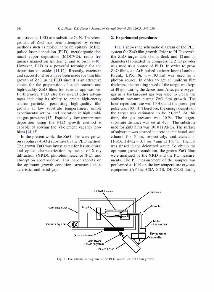
Fig. 1. The schematic diagram of the P
2. Experimental procedures
Fig. 1 shows the schematic diagram of the PLDsystem for ZnO film growth. Prior to PLD growth,the ZnO target disk (3mm thick and 12mm indiameter) fabricated by compressing ZnO powderwas used as a source of PLD. In order to growZnO films, an ArF pulsed excimer laser (LambdaPhysik, LPX110i, l ¼ 193 nm) was used as aphoton source. In order to get an uniform filmthickness, the rotating speed of the target was keptat 40 rpm during the deposition. Also, pure oxygengas as a background gas was used to create theambient pressure during ZnO film growth. Thelaser repetition rate was 10Hz, and the power perpulse was 100mJ. Therefore, the energy density onthe target was estimated to be 2 J/cm2. At thistime, the gas pressure was 10 Pa. The target-substrate distance was set at 4 cm. The substrateused for ZnO films was (0 0 0 1) Al2O3. The surfaceof substrate was cleaned in acetone, methanol, andethanol for 5min, respectively, and etched inH2SO4:H2PO4 ¼ 3:1 for 7min at 150 1C. Then, itwas rinsed in the deionized water. To obtain theoptimum growth condition, the grown ZnO filmswere analyzed by the XRD and the PL measure-ments. The PL measurement of the samples wasperformed at 10K on the low temperature cryostatequipment (AP Inc. CSA 202B, DE 202S) during
LD system for ZnO film growth.

ARTICLE IN PRESS
K.J. Hong, T.S. Jeong / Journal of Crystal Growth 280 (2005) 545–550 547
the excitement of the He–Cd laser (Kimmon,442 nm, 50mW). The thickness of the ZnO filmswas measured by an a-step profilometer (Tenco, a-step 200). In addition, the electric properties wereachieved by Hall effect measurement of van derPauw method at various temperatures. To mea-sure the energy band gap, the optical absorptionexperiment was performed on a UV–VIS–NIRspectrophotometer (Hitachi, U-3501) for a rangeof 360–370 nm at various temperatures from 10 to293K.
Table 2
Optimum growth conditions of the PLD method for the high
quality ZnO films
Parameters Optimum values
Substrate temperature 400 1C
Rotating speed of target 40 rpm
Laser repetition rate 10Hz
Power per pulse 100mJ
Background gas pressure (O2) 10 Pa
Target-substrate distance 4 cm
3. Results and discussion
3.1. Growth parameters and structural properties
ZnO films were grown by varying the substratetemperature from 380 to 420 1C. To find theoptimum growth condition, the PL measurementon the grown films was performed at 10K, and theXRD experiment was also conducted at roomtemperature. Among the PL spectra obtained, theemissions caused by the exciton were used topredict the crystal quality criterion of the grownfilm because the exciton could only be observed inthe less defective crystal at low temperature.Therefore, free exciton (Ex) and neutral donorbound exciton (D1, X) emissions were used for theoptimum growth condition. And self-activated(SA) emission was also checked. Ordinarily, theintensity of exciton has a tendency to increase, andthe SA peak is inclined to decrease in the quality ofcrystal at low temperature. In addition, theintensity and the full-width half-maximum(FWHM) of the XRD curves were used for crystalquality evaluation of ZnO films. As shown in
Table 1
Comparison of the PL intensity and the XRD curves as a function o
Substrate temperature (1C) Intensity of PL at 10K
Ex (D1, X)
380 0 63
400 48 108
420 0 77
Table 1, the highest (D1, X) peak and the veryweak SA peak were observed in the film which wasgrown while the substrate temperature was kept at400 1C. Also, the Ex emission was observed only atthe substrate temperature of 400 1C. This observa-tion indicates that the ZnO film grown at 400 1Chas a very high quality because the emission peakof the free exciton can be observed only under thecondition of a long-range Coulomb couplingbetween the electron and the hole. Thus, to certifycrystalline quality, the evaluation of ZnO films wasenhanced by the XRD method. As shown in Table1, the highest intensity and the narrowest FWHMof XRD curve were observed in ZnO films grownat 400 1C. To grow the ZnO films, the optimumtemperature of the substrate was found to be400 1C. Table 2 presents the optimum growthconditions for high quality ZnO films using thePLD method. Therefore, ZnO films grown by thegrowth conditions in Table 2 were obtained to thethickness of 2.9 mm and the growth rate of1.45 mm/h. Here, the growth rate of the film iscomparatively high. The PLD growth method isknown to deliver more energetic atomic species tothe substrate several tens or hundreds times higher
f substrate temperature (arbitrary units)
XRD
SA Intensity (� 104) FWHM
10 0.85 0.2191
18 1.34 0.2011
28 1.10 0.2081

ARTICLE IN PRESS
Fig. 2. The surface morphology of SEM on ZnO film grown
under optimized conditions.
Fig. 3. The XRD spectrum of ZnO film grown under optimized
conditions.
K.J. Hong, T.S. Jeong / Journal of Crystal Growth 280 (2005) 545–550548
than MBE. Fig. 2 shows the surface morphologyof scanning electron microscope (SEM) on ZnOfilm grown under optimized conditions. As shownin Fig. 2, the morphology revealed a very smoothsurface, and it was consisted of nano-size crystal-lites having a size of 40–50 nm. Fig. 3 presents theXRD spectrum of ZnO film grown underoptimized conditions. These patterns correspondto the diffraction peaks of the ZnO (0 0 0 2)and Al2O3 (0 0 0 6). The intensity of ZnO (0 0 0 2)peak located at 2y of 34.4771 is very sharpand dominant. This indicates that the film isstrongly oriented to the c-axis of hexagonalstructure and also crystallized under constraintscreated by the substrate. Therefore, it meansthat ZnO film is epitaxially crystallized eventhough the lattice mismatch between ZnO andAl2O3 is very large. The FWHM for 1y curveof (0 0 0 2) peak is 0.2011. This value is betterthan that of 0.351 obtained from the PLD methodby Ryu et al. [16], and similar to the values of0.1971 grown from MBE method by Wang et al.[17] and 0.1781 grown from MOCVD methodby Ye et al. [18]. Therefore, it implies that thefilms grown by the PLD method are comparableto those grown by MBE and MOCVD onAl2O3 substrate in spite of comparatively highgrowth rate. Furthermore, by conducting the post-growth annealing, it is suggested that the crystal
quality of the annealed films in comparison withthe as-grown ZnO can be remarkably improved.In order to evaluate the mean crystallite size ofthe film, it was generally used by the Scherrerformula [19]
D ¼ 0:94l=ðB cos yÞ, (1)
where l, y, and B are the X-ray wavelength(0.15405 nm), the Bragg diffraction angle, and theFWHM value on (0 0 0 2) peak of 34.4771 inradians, respectively. The mean crystallite sizeobtained from Eq. (1) was estimated to be about41 nm. Therefore, the crystalline size evaluated byXRD was consistent with the SEM result.From the Hall effect measurement, the mea-
sured mobility and carrier density at 293K were299 cm2/V sec and 8:27� 1016 cm�3, respectively.The mobility tended to increase during thedecrease to the temperature of 100K, and there-after, it decreased. At the apex of 100K, it showeda largest value of 998 cm2/V sec. The grown ZnOfilm was confirmed to be an n-type. The grownsample was always the n-type owing presumably toslight stoichiometric deviations originating froman excess of oxygen vacancies.
ARTICLE IN PRESS
K.J. Hong, T.S. Jeong / Journal of Crystal Growth 280 (2005) 545–550 549
3.2. Optical absorption measurement
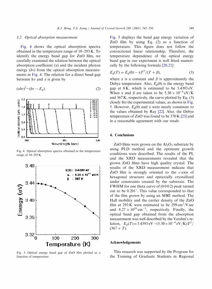
Fig. 4 shows the optical absorption spectraobtained in the temperature range of 10–293K. Toidentify the energy band gap for ZnO film, wecarefully examined the relation between the opticalabsorption coefficient (a) and the incident photonenergy (hn) from the optical absorption measure-ments in Fig. 4. The relation for a direct band gapbetween hn and a is given by
ðahnÞ2�ðhn� EgÞ. (2)
Fig. 4. Optical absorption spectra obtained in the temperature
range of 10–293K.
Fig. 5. Optical energy band gap of ZnO film plotted as a
function of temperature.
Fig. 5 displays the band gap energy variation ofZnO film by using Eq. (2) as a function oftemperature. This figure does not follow theconvectional linear relationship. Therefore, thetemperature dependence of the optical energyband gap in our experiment is well fitted numeri-cally by the following formula [20,21]:
EgðTÞ ¼ Egð0Þ � aT2=ðT þ bÞ, (3)
where a is a constant and b is approximately theDebye temperature. Also, Eg(0) is the energy bandgap at 0K, which is estimated to be 3.4393 eV.When a and b are taken to be 5:30� 10�4 eV=Kand 367K, respectively, the curve plotted by Eq. (3)closely fits the experimental values, as shown in Fig.5. However, Eg(0) and a were nearly consistent tothe values obtained by Ray [22]. Also, the Debyetemperature of ZnO was found to be 370K [23] andin a reasonable agreement with our result.
4. Conclusions
ZnO films were grown on the Al2O3 substrate byusing PLD method and the optimum growthconditions were described. The results of the PLand the XRD measurements revealed that thegrown ZnO films have high quality crystal. Theresults of the XRD measurement indicate thatZnO film is strongly oriented to the c-axis ofhexagonal structure and epitaxially crystallizedunder constraints created by the substrate. TheFWHM for one theta curve of (0 0 0 2) peak turnedout to be 0.2011. This value corresponded to thatof the film grown by using an MBE method. TheHall mobility and the carrier density of the ZnOfilm at 293K were estimated to be 299 cm2/V secand 8:27� 1016 cm�3, respectively. Finally, theoptical band gap obtained from the absorptionmeasurement was well described by the Varshni’s re-lation, EgðTÞ¼3:4393 eV�ð5:30�10�4 eV=KÞT2=ð367þ TÞ.
Acknowledgements
This research was supported by the Program forthe Training of Graduate Students in Regional

ARTICLE IN PRESS
K.J. Hong, T.S. Jeong / Journal of Crystal Growth 280 (2005) 545–550550
Innovation which was conducted by the Ministryof Commerce, Industry and Energy of the KoreanGovernment.
References
[1] B. Lin, Z. Fu, Y. Jia, Appl. Phys. Lett. 79 (2001) 943.
[2] K. Ueda, H. Tabata, T. Kawai, Appl. Phys. Lett. 79 (2001)
988.
[3] Z.K. Tang, G.K.L. Wong, P. Yu, M. Kawasaki,
A. Ohtomo, H. Koinuma, Y. Segawa, Appl. Phys. Lett.
72 (1998) 3270.
[4] D.M. Bagnall, Y.F. Chen, Z. Zhu, T. Yao, M.Y. Shen,
T. Goto, Appl. Phys. Lett. 73 (1998) 1038.
[5] M.-S. Wu, A. Azuma, T. Shiosaki, A. Kawabata, J. Appl.
Phys. 62 (1987) 2482.
[6] F.S. Hickernell, J. Appl. Phys. 41 (1973) 1061.
[7] Y. Chen, D.M. Bagnall, Z. Zhu, T. Sekiuchi, K. Park,
K. Hiraga, T. Yao, S. Koyama, M.Y. Shen, T. Goto,
J. Crystal Growth 181 (1997) 165.
[8] F.T.J. Smith, Appl. Phys. Lett. 43 (1983) 1108.
[9] K.B. Sundaram, A. Khan, Thin Solid Films 295 (1997) 87.
[10] Y. Nakata, T. Okada, M. Maeda, Appl. Surf. Sci. 197/198
(2002) 368.
[11] Y. Nakata, G. Soumagne, T. Okada, M. Maeda, Appl.
Surf. Sci. 129 (1998) 650.
[12] C.V. Ramana, R.J. Smith, O.M. Hussain, C.M. Julien,
Mater. Sci. Eng. B 111 (2004) 218.
[13] L.N. Dinh, M.A. Schildbach, M. Balooch, W. McLean II,
J. Appl. Phys. 86 (1999) 1149.
[14] M. Chu, S. Terterian, D. Ting, C.C. Wang, H.K.
Gurgenian, S. Mesropian, Appl. Phys. Lett. 79 (2001)
2728.
[15] S.D. Setzler, M. Moldovan, Z. Yu, T.H. Myers,
N.C. Giles, L.E. Halliburton, Appl. Phys. Lett. 70 (1997)
2274.
[16] Y.R. Ryu, S. Zhu, J.M. Wrobel, H.M. Jeong, P.F. Miceli,
H.W. White, J. Crystal Growth 216 (2000) 326.
[17] X. Wang, S. Yang, J. Wang, M. Li, X. Jiang,
G. Du, X. Liu, R.P.H. Chang, J. Crystal Growth 226
(2001) 123.
[18] J. Ye, S. Gu, S. Zhu, T. Chen, L. Hu, F. Qin, R. Zhang, Y.
Shi, Y. Zheng, J. Crystal Growth 243 (2002) 151.
[19] B.D. Cullity, Elements of X-ray Diffractions, Addition-
Wesley, Reading, MA, 1978, p. 102.
[20] Y.P. Varshni, Physica 34 (1967) 149.
[21] K.J. Hong, T.S. Jeong, C.J. Yoon, Y.J. Shin, J. Crystal
Growth 218 (2000) 19.
[22] B. Ray, II–VI Compounds, Pergamon, Oxford, 1969,
p. 54.
[23] E. Mollwo, in: O. Madelung (Ed.), Landolt-Bornstein:
Numerical Data and Functional Relationships in
Science and Technology, vol. 17h, Springer, Berlin, 1982,
p. 35.