sputter deposition of zno thin films
TRANSCRIPT
SPUTTER DEPOSITION OF ZNO THIN FILMS
By
LOREN WELLINGTON RIETH
A DISSERTATION PRESENTED TO THE GRADUATE SCHOOLOF THE UNIVERSITY OF FLORIDA IN PARTIAL FULFILLMENT
OF THE REQUIREMENTS FOR THE DEGREE OFDOCTOR OF PHILOSOPHY
UNIVERSITY OF FLORIDA
2001

Copyright 2001
by
Loren Wellington Rieth

Dedicated to my wife, Wendy; to my family, Herb Jr., Sheri, and Herb III; and themother of us all.

iv
ACKNOWLEDGMENTS
Dr. Holloway has been my mentor for the last seven years. His knowledge of
science both humbles and enlightens me. His dedication to his profession and students
is reflected in numerous awards, publications, and the common occupation of his car in
the coveted parking spot directly in front of Rhines Hall. His patience and guidance have
been invaluable.
My wife Wendy has been a source of so many things to me in the process of
graduate school. Motivation, encouragement, strength, and love have all been given in
excess. Her patience and support have helped ease the writing process and kept the basic
necessities of life continuing as large portions of my time focused on completing this
work.
It would be a travesty to call Ludie Harmon a secretary. So much of smooth day
to day operation depends on her competence. More than this, she reminds us that we are
people, and there are cares in the world which should be balanced with a career.
Additionally, there is the candy jar and the weekly cookies that magically appear for
which no amount of thanks is sufficient.
There are many people to thank in the Holloway group. In particular is Billie
Abrams, whose interactions have enriched my graduate career and life. Dr. Mark
Davidson and his unique talents in coaxing dead equipment to life and knowledge of
scientific lore have been an asset to so many in our department including me. So
much of what works does so because he works hard. My seven year tenure means I can

v
name a lot of names of people who have all helped in their ways, and include (in no
particular order) Sushil, Craig, Heather, John, Troy, Big and Little Joe, Tracy, Brent,
Eric, Lizandra, Jae-Hyun, Joon-Bo, Heesun, Sean, Jeff, Mike, Vaidy, Maggie, Scott,
Jacque, Lisa, Nagraj, JP, Caroline, Huang, Billy, Alex, Suku, Serkan, Lei . . . .
Of course no acknowledgement would be complete without thanking my parents.
To my mom, whose own graduate career I waylaid for 20 years, and my dad, who just
managed to finish before there was me, I of course owe everything. They not only
brought me into the world but have endeavored to help me through it.

vi
TABLE OF CONTENTSpage
LIST OF TABLES ......................................................................................................... ix
LIST OF FIGURES......................................................................................................... x
ABSTRACT ................................................................................................................ xiv
1 INTRODUCTION AND MOTIVATION..................................................................... 1
2 LITERATURE REVIEW ............................................................................................. 5
2.1 Introduction...........................................................................................................52.2 Photovoltaic Devices .............................................................................................5
2.2.1 History............................................................................................................52.2.2 Device Physics................................................................................................82.2.3 Thin Film Solar Cells.................................................................................... 122.2.4 Transparent Conducting Electrode (TCE) ..................................................... 17
2.3 Transparent Conducting Oxides........................................................................... 212.3.1 Background .................................................................................................. 212.3.2 Electrical Properties of TCOs........................................................................ 272.3.3 Optical Properties ......................................................................................... 39
2.4 Sputter Deposition ............................................................................................... 472.4.1 Background .................................................................................................. 472.4.2 Thin Film Coalescence.................................................................................. 542.4.3 Negative Ion Resputtering............................................................................. 58
3 EXPERIMENTAL METHODS.................................................................................. 63
3.1 Introduction......................................................................................................... 633.2 Thin Film Deposition........................................................................................... 63
3.2.1 New Oxide Sputtering System ...................................................................... 633.2.2 Description of the Sputtering System ............................................................ 673.2.3 Substrate Cleaning ........................................................................................ 68
3.3 Electrical Characterization................................................................................... 693.3.1 Hall Measurements ....................................................................................... 693.3.2 Four Point Probe........................................................................................... 71
3.4 Structural Characterization .................................................................................. 723.4.1 Profilometry.................................................................................................. 723.4.2 X-Ray Diffraction......................................................................................... 723.4.3 Atomic Force Microscopy............................................................................. 733.4.4 Auger Electron Spectroscopy........................................................................ 75

vii
3.4.5 X-ray Photoelectron Spectroscopy ................................................................ 763.4.6 Secondary Ion Mass Spectrometry ................................................................ 79
3.5 Optical Properties ................................................................................................ 803.5.1 Spectrophotometry........................................................................................ 803.5.2 Fourier Transform Infrared Spectroscopy...................................................... 80
3.6 Experimental Procedures ..................................................................................... 813.6.1 Affect of Annealing Ambient on the Properties of ZnO:Al............................ 813.6.2 Development of Properties in Very Thin ZnO:Al Films ................................ 833.6.3 Negative Ion Resputtering in Sputter Deposition of ZnO:Al Films................ 84
4 AFFECT OF ANNEALING AMBIENT .................................................................... 89
4.1 Background ......................................................................................................... 894.2 Results................................................................................................................. 90
4.2.1 Structural Characterization............................................................................ 904.2.2 Electrical Characterization ............................................................................ 994.2.3 Optical Characterization ............................................................................. 102
4.3 Discussion ......................................................................................................... 1084.3.1 Structural Properties ................................................................................... 1084.3.2 Electrical Properties .................................................................................... 1124.3.3 Optical Properties ....................................................................................... 120
4.4 Summary ........................................................................................................... 122
5 DEVELOPMENT OF ELECTRICAL AND MICROSTRUCTURAL PROPERTIES INVERY THIN ZNO:AL FILMS.................................................................................... 124
5.1 Background ....................................................................................................... 1245.2 Results............................................................................................................... 125
5.2.1 Structural Characterization.......................................................................... 1255.2.1.1 Profilometry......................................................................................... 1255.2.1.2 Atomic force microscopy ..................................................................... 1265.2.1.3 Auger electron spectroscopy ................................................................ 131
5.2.2 Electrical Characterization .......................................................................... 1375.3 Discussion ......................................................................................................... 141
5.3.1 Surface Morphology ................................................................................... 1415.3.2 Electrical Characterization .......................................................................... 150
5.4 Summary ........................................................................................................... 156
6 NEGATIVE ION RESPUTTERING ........................................................................ 159
6.1 Background ....................................................................................................... 1596.2 Experiment Results............................................................................................ 162
6.2.1 Profilometry................................................................................................ 1626.2.2 Electrical Characterization .......................................................................... 165
6.2.3 Secondary Ion Mass Spectrometry Results .............................................. 1756.2.4 X-ray Photoelectron Spectroscopy Results .............................................. 180
6.2.5 X-ray Diffraction Results ............................................................................ 183

viii
6.2.4 Atomic Force Microscopy Results .............................................................. 1956.3 Discussion of RF Power Experiment.................................................................. 199
6.3.1 Model of the Effects of Negative Ion Resputtering on Electrical Properties. 1996.3.2 Region I...................................................................................................... 207
6.3.2.1 Profilometry (Region I) ........................................................................ 2076.3.2.2 Resistivity effects (Region I) ................................................................ 2106.3.2.3 Hall carrier concentration (Region I) .................................................... 2126.3.2.4 Hall mobility (Region I) ....................................................................... 2166.3.2.5 Secondary ion mass spectrometry......................................................... 2196.3.2.6 X-ray photoelectron spectroscopy ........................................................ 2206.3.2.7 X-ray diffraction (Region I) ................................................................. 2226.3.2.8 Atomic force microscopy (Region I) .................................................... 229
6.3.3 Region II..................................................................................................... 2306.3.3.1 Profilometry (Region II)....................................................................... 2306.3.3.2 Resistivity effects (Region II)............................................................... 2316.3.3.3 Hall carrier concentration (Region II)................................................... 2336.3.3.4 Hall mobility (Region II)...................................................................... 2346.3.3.5 X-ray diffraction (Region II) ................................................................ 2346.3.3.6 Atomic force microscopy (Region II) ................................................... 236
6.3.4 Region III ................................................................................................... 2366.3.4.1 Profilometry (Region III) ..................................................................... 2366.3.4.2 Resistivity effects (Region III) ............................................................. 2376.3.4.3 Hall carrier concentration (Region III).................................................. 2376.3.4.4 Hall mobility (Region III) .................................................................... 2396.3.4.5 X-ray diffraction (Region III) ............................................................... 2406.3.4.6 Atomic force microscopy (Region III).................................................. 241
6.4 Summary ....................................................................................................... 241
7 CONCLUSIONS...................................................................................................... 243
7.1 Negative Ion Resputtering ................................................................................. 2437.2 Chemisorbed Oxygen ........................................................................................ 2477.3 Property Development in Thin ZnO:Al Thin Films ............................................ 2487.4 Future Work ...................................................................................................... 250
LIST OF REFERENCES ............................................................................................ 253
BIOGRAPHICAL SKETCH....................................................................................... 262

ix
LIST OF TABLES
Table Page
2-1. Materials parameters for chalcopyrite ternary compositions. ..................................... 16
2-2. History of processes for making transparent conductors. ........................................... 23
2-3. Compilation of electrical data for sputter deposited ZnO thin films with severaldifferent dopants. ............................................................................................. 25
3-1. Parameters used for Auger electron sepectroscopy sputter depth profiles................... 77
3-2. Parameters used to collect XPS multiplex scans. ....................................................... 78
4-1. JCPDS powder XRD reference data for Wurtzite ZnO. ............................................. 90
4-2. Quantified XRD data from (100) diffraction peak...................................................... 97
4-3. Quantified XRD data from (002) diffraction peak...................................................... 97
4-4. Resistivity data from before and after heat treatment measured by four point probeas a function of position and gas ambient used. ................................................ 100
4-5. Changes in resistivity with 400°C one hour annealing. .............................................. 102
4-6. Quantified optical band gap (Eg) data from before and after annealing at 400°C forone hour........................................................................................................... 108
5-1. Sample indentification, deposition time, and film thickness........................................ 126
6-1. Atomic concentrations from XPS multiplex data for as deposited and sputter etchedsamples. ........................................................................................................... 181

x
LIST OF FIGURES
Figure Page
1-1. Total and renewable energy consumption in the United States................................... 2
2-1. Schematic cross sectional view of a typical CIS based thin film solar cell structure. .. 6
2-2. Progress in improving efficiency of solar cells .......................................................... 7
2-3. Irradiance of the solar spectrum................................................................................. 9
2-4. Theoretical plot of the I-V characteristics for a typical Si solar cell ........................... 10
2-5. Band diagram of a typical n-p homojunction solar cell .............................................. 11
2-6. One unit cell of the CuInSe2 chalcopyrite crystal structure ........................................ 16
2-7. Conduction and valence band alignments of a typically CIS based solar cell ............. 18
2-8. Equivalent circuit diagram for a solar cell ................................................................. 19
2-9(a-b). Influence of a solar cell’s series resistance ......................................................... 20
2-10. Decreasing resistivity of transparent conducting oxides........................................... 24
2-11. Schematic representation of the influence of grain boundaries................................. 33
2-12. Illustration of the chemisorbed oxygen mechanism for solid state gas sensors ......... 34
2-13(a-c). Theoretical plots of relationships between electrical and optical properties....... 43
2-14. Illustration of the Burstein-Moss shift ..................................................................... 45
2-15. Generation of interference colors or Fabry-Perot oscillations.................................... 46
2-16. Plot of the power cosine distribution........................................................................ 49
2-17(a-b). Illustrations of planar sputter deposition sources .............................................. 50
2-18(a-b). Illustration of the negative self bias formation during RF sputter deposition..... 54
2-19. Representation of the influences of surface forces on the morphology of adeposited film .................................................................................................. 55

xi
2-20. A structural zone model showing changes in thin film morphology ......................... 56
2-21. The hexagonal wurtzite crystal structure for ZnO in the zincite phase...................... 57
2-22. Schematic of the negative ion generation and acceleration process during sputterdeposition of ZnO:Al thin films. ...................................................................... 59
2-23. Theoretical plot of the mean free path of an Ar atom ............................................... 60
3-1(a-d). Schematic diagram and pictures of the new oxide sputtering system ................... 65
3-2. Cross-sectional view of the sputter deposition system known as “Rusty”................... 68
3-3. Positions on the 2.5 x 5 cm substrate where four point probe data were collected ...... 82
3-4. Top-view of the deposition geometry used for the investigation of negative ionresputtering...................................................................................................... 85
4-1(a-b) X-ray diffraction spectra from before and after a ZnO:Al thin film is annealed innitrogen ........................................................................................................... 92
4-2(a-b) X-ray diffraction spectra from before and after a ZnO:Al thin film is annealed informing gas...................................................................................................... 93
4-3(a-b) X-ray diffraction spectra from before and after a ZnO:Al thin film is annealed instagnant air ...................................................................................................... 94
4-4(a-b) X-ray diffraction spectra from before and after a ZnO:Al thin film is annealed inoxygen............................................................................................................. 95
4-5(a-b) X-ray diffraction spectra from before and after a ZnO:Al thin film used as acontrol sample ................................................................................................. 96
4-6(a-b). Transmission spectra of uncoated and ZnO:Al coated soda-lime glass substrateswith data from before and after annealing of the coated sample........................ 103
4-6(c-d). Transmission spectra of uncoated and ZnO:Al coated soda-lime glass substrateswith data from before and after annealing of the coated sample........................ 104
4-6(e). Transmission spectra of uncoated and ZnO:Al coated soda-lime glass substrateswith no annealing of the coated sample for a control sample ............................ 105
4-7. Plots of the absorption squared (A2) versus wavelength to determine changes inoptical band gap of the ZnO:Al film with annealing ......................................... 105
4-8. Fourier transform infrared spectra taken in reflection mode....................................... 109
5-1. Z range, “grain size”, and RMS roughness data for ZnO:Al thin films....................... 127

xii
5-2(a-d). AFM micrographs from a 0.5 x 0.5 µm area ...................................................... 129
5-2(e-h). AFM micrographs from a 0.5 x 0.5 µm area for ZnO:Al thin films .................... 130
5-3(a-c). AES data from the 18 Å thick ZnO:Al sample.................................................... 132
5-4(a-c). AES data from the 105 Å thick ZnO:Al sample.................................................. 133
5-5(a-c). AES data from the 525 Å thick ZnO:Al sample.................................................. 134
5-6. Percentage of the soda-lime glass substrate covered by the sputter deposited ZnO:Althin film........................................................................................................... 138
5-7(a-c). Electrical data for ZnO:Al thin films plotted as a function of film thickness ....... 140
5-8. Schematic representation of the constant volume transformation ............................... 143
5-9(a-b). Relationships between surface coverage, film thickness (t in Å), and nucleusradius (Å)......................................................................................................... 144
5-10. Illustration of carrier trajectories based on the Fuchs and Sondheimer model........... 153
5-11. Calculated plot of the resistivity ratio between the thin films ................................... 153
6-1. Cross-sectional view of the sputter deposition geometry............................................ 161
6-2. Measured thickness of the ZnO:Al thin film .............................................................. 163
6-3. Deposition rate of ZnO:Al......................................................................................... 163
6-4. Deposited molecular flux of ZnO:Al ......................................................................... 165
6-5. Deposition rate ratio between 250 W/1000 W and 500 W/1000 W conditions ........... 166
6-6. Resistivity of ZnO:Al thin films ................................................................................ 167
6-7. Resistivity of ZnO:Al thin films with 500 W data offset by 3.2 cm............................ 167
6-8. Resistivity of the deposited ZnO:Al thin film plotted versus thickness....................... 169
6-9(a-b). Carrier concentration of ZnO:Al thin films ........................................................ 171
6-10(a-b). Hall mobility of ZnO:Al thin films................................................................... 174
6-11(a-b). SIMS depth profile data for ZnO:Al films deposited at 250 W ......................... 177
6-12(a-b). SIMS depth profile data for ZnO:Al films deposited at 500 W ......................... 178
6-13(a-b). SIMS depth profile data for ZnO:Al films deposited at 1000 W ....................... 179

xiii
6-14(a-b). XPS multiplex spectra of the O (1s) peak......................................................... 182
6-15(a-b). XRD spectra from ZnO:Al thin films deposited at 250 W ................................ 184
6-16(a-b). XRD spectra from ZnO:Al thin films deposited at 500 W ................................ 185
6-17(a-b). XRD spectra from ZnO:Al thin films deposited at 1000 W .............................. 186
6-18(a-b). Maximum XRD peak intensity of the (002) peak for ZnO:Al thin films ........... 189
6-19(a-b). Position of the ZnO:Al (002) peak in 2θ (degrees) plotted ............................... 191
6-20(a-b). FWHM of the (002) ZnO:Al XRD peak........................................................... 193
6-21(a-c). Process used to quantify “grain size” from AFM micrographs.......................... 196
6-22(a-b). “Grain size” of the ZnO:Al thin films .............................................................. 198
6-23(a-b). RMS roughness of the ZnO:Al thin films......................................................... 200
6-24. Resistivity of the ZnO:Al thin film .......................................................................... 213
6-25(a-b). Corrected carrier concentration from Hall measurements for ZnO:Al thinfilms ................................................................................................................ 214
6-26(a-b). Corrected Hall mobility for ZnO:Al thin films ................................................. 217

xiv
Abstract of Dissertation Presented to the Graduate Schoolof the University of Florida in Partial Fulfillment of theRequirements for the Degree of Doctor of Philosophy
SPUTTER DEPOSITION OF ZNO THIN FILMS
By
Loren Wellington Rieth
December 2001
Chairman: Paul H. HollowayMajor Department: Materials Science and Engineering
Sputter deposition and characterization of ZnO thin films for application as a
transparent conducting electrode have been studied. The effects of gas ambient upon
annealed film properties, evolution of structural and electrical properties of very thin ZnO
films, and the influence of negative ion resputtering on the thin film properties were
investigated.
For annealing sputter deposited ZnO thin films, the gas ambient in the quartz tube
furnace was found to be a critical parameter for the resistivity of ZnO:Al thin films.
Annealing films in forming gas (N2/H2 90%/10%) at 400°C for 60 minutes was found to
reduce the resistivity of the films by up to two orders of magnitude with a minimum
value of 2x10⁻³ Ω·cm. Optical measurements indicate an increase in carrier concentration
is responsible for the decreased resistivity.
The nucleation of ZnO:Al films on glass substrates occurs by the island (Volmer-
Webber) mechanism. Films less than 1000 Å thick were found to have higher resistivity

xv
due to decreased carrier concentration postulated to result from carrier depletion by
chemisorbed oxygen. The minimum resistivity achieved was 4.3x10⁻³ Ω·cm at a film
thickness of 1580 Å.
The effects of negative ion resputtering on the structural and electrical properties
of deposited ZnO:Al films were evaluated. A model incorporating system geometry,
deposition conditions, negative ion resputtering, and film thickness was developed to
explain the structural and electrical properties of the deposited films. The model defines
Regions I, II, and III, with the resistivity in Region I between 4.3x10⁻³ to 1.2x10⁻² Ω·cm,
a carrier concentration of between 7.2x10¹⁹ to 3.2x1020 cm-3, and mobilities of
approximately 7 cm2/V·s. In Region II, the resistivity decreases to 1.5x10⁻³ Ω·cm, due to
increased carrier concentrations of 5x1020 cm-3, while mobility remains near 7 cm2/V·s.
For Region III resistivity increases to greater than 10 Ω·cm, due to carrier concentrations
as low as 1.0x1019 cm-3, and mobilities as low as 1.5 cm2/V·s. Low carrier concentrations
in Region I result from compensation by native defects created by negative ion
resputtering, while low carrier concentrations in Region III result from chemisorbed
oxygen species.

1
CHAPTER 1INTRODUCTION AND MOTIVATION
The need for electrical power is the fundamental motivating force for the research
presented in this work. Department of Energy statistics for total energy consumption in
the US are presented in Figure 1-1, and show a steady increase with time since 1949.
The vast majority of this energy is produced by fossil fuels and nuclear power as can be
seen from the small fraction of the total energy consumption supplied by renewable
energy sources. At current consumption rates, fossil and nuclear fuel supplies will last on
the order of decades to centuries. Significant price increases will occur for energy
produced from fossil and nuclear fuels as these resources are depleted. Additionally, use
of fossil and nuclear fuels results in environmental degradation during procurement,
consumption, and waste disposal. Therefore the long-term energy security of this country
and the world at large is dependent on use of sustainable quantities of energy generated
from renewable sources. Renewable energy sources currently under development and in
use include hydroelectric, geothermal, wind, biomass, nuclear fusion, and solar
(photovoltaic and thermal).
Photovoltaic cells, more commonly known as solar cells, are based on the ability
of certain materials and structures to generate electrical power when exposed to light.
Modern solar cells are based on semiconducting materials. Two classes of solar cells are
bulk and thin cells, and are distinguished by the thickness of the material that absorbs the
light to generate electricity. Bulk solar cells rely on semiconducting wafers on the order
of half a millimeter in thickness. Thin film solar cells are fabricated by depositing layers

2
0
20000000
40000000
60000000
80000000
100000000
120000000
1949 1959 1969 1979 1989 1999
Year
Bill
ions
of
BT
Us Energy Consumption
Renewable EnergyConsumption
Figure 1-1. Total and renewable energy consumption in the United States of America inbillions of BTU versus time in years [1].
of semiconducting materials of a thickness on the order of 1 µm onto inexpensive
substrates such as glass, plastic, or metal foils. Significantly lower production costs are
possible due to 100 times smaller volume of semiconducting material used in thin film
cells. It is the production cost per peak watt ($/kWp) that is a critical figure of merit. In
order to be competitive with current power pricing, a rough threshold of $3/kWp must be
surpassed for areas serviced by the power “grid.” Current applications where solar cells
are cost effective include remote locations and developing countries, where the power
infrastructure is not established.
Thin film solar cells are based on a number of semiconducting materials,
including copper chalcogenides, cadmium telluride, and amorphous silicon. Copper
chalcogenides in the Cu(In,Ga)Se2 or CIGS system have demonstrated 18.8% conversion
efficiency for research size cells [2]. Advantages of this materials system leading to high

3
efficiencies include a large optical absorbance (α~105 cm-1) from a direct band gap,
ability to change the band gap by control of the stoichiometry, a large minority carrier
lifetime, and compatibility with thin film deposition techniques [3,4].
Because semiconducting layer of thin film solar cells often have a high resistance,
a front transparent conducting electrode (TCE) is critical to cell efficiency. Thin films of
ZnO are almost exclusively used as the TCE for thin film solar cells based on CIGS.
Further improvement of the properties of ZnO thin films is recognized as necessary for
further improvement of large area production modules [5]. Use of ZnO as a TCE is
attractive because of its match to the electrical properties of other layers in a CIGS device
and the low price of zinc especially compared to the semiprecious metal indium. Zinc
oxide is also compatible with large area thin film deposition techniques, Zn and O are
isoelectronic with the CdS layer ZnO is deposited upon, and has optical and electrical
properties that are competitive with other TCO materials.
The focus of this research is to improve the knowledge of the relationships
between the thin film deposition process and the structure and properties of the resulting
ZnO films. This knowledge can then be used to improve the properties of ZnO thin
films, and decrease the effort needed to optimize film properties in the future. Based on
production and performance considerations, sputter deposition of ZnO thin films has
yielded the best results, and will therefore be the technique used in this work. Key issues
investigated are the influence of sputtering process variables on the properties of the
resulting films. The process variables for the sputtering process influence the
microstructure of the deposited film, which in turn dictates the electrical and optical
properties. A review of the literature is present in Chapter 2, and provides background
4
information on CIGS based thin film solar cells, ZnO window layers, and the sputtering
process. The experimental method is discussed in Chapter 3, and relates the methods,
conditions, and characterization tools used to determine the relationships between the
deposition process and film properties. Results and discussion from an experiment
designed to investigate the influence of annealing and the gas ambient used for annealing
is presented in Chapter 4. Results and discussion presented in Chapter 5 cover an
experiment designed to investigate the development of properties in very thin ZnO:Al
thin films. The experiment discussed in Chapter 6 is designed to investigate negative ion
resputtering and the mechanisms by which it influences the properties of deposited films,
and film thickness effects on electrical properties in very thin films. The overall
conclusions drawn from this work are communicated in Chapter 7.
As a final note, this work is primarily motivated by the application of thin film
solar cells. It is worth noting that there are many applications for zinc oxide thin films.
Several examples include gas sensors [6-9], surface acoustic wave devices [10], structural
e-glass coatings [11,12], and with the advent of p-type ZnO wide band gap electronic
structures [13].

5
CHAPTER 2LITERATURE REVIEW
2.1 Introduction
The focus of this study is the relationships between the sputter deposition process
and post deposition heat treatments to the structural, electrical, and optical properties of
deposited ZnO:Al thin films. The objective is to improve properties of the ZnO:Al films
with respect to application as a transparent conducting electrode (TCE) to CuInSe2 (CIS)
thin film solar cells. This chapter reviews background information and concepts
including the basics of solar cells, transparent conducting oxides, and sputter deposition.
The section on solar cells covers history, basic device physics, and influence of the TCE
on solar cells. A cross-sectional view of a typical CIS based solar cell structure is
presented in Figure 2-1. The transparent conducting oxide section reviews the history of
transparent conductors and the principles of their electrical and optical properties. The
topics covered in the sputter deposition section include the sputtering process in several
important geometries, thin film coalescence, and negative ion resputtering. Specific
information regarding ZnO will be worked into all of these themes.
2.2 Photovoltaic Devices
2.2.1 History
The photovoltaic or Dember Effect is defined as “providing a source of electric
current under the influence of light or similar radiation.” [14] Becquerel discovered

6
Grid Metalization
Figure 2-1. Schematic cross sectional view of a typical CIS based thin film solar cellstructure.
this effect in 1839, when he noticed power generation from metal plates in electrolyte
solutions. In 1876, power generation was reported from selenium, the first solid state
photovoltaic device [4]. The first modern semiconductor solar cell was developed in
1954 by Chapin, Fuller, and Pearson, and was based on a p-n junction formed in silicon
[15]. This quantum leap of technology in conjunction with the needs of the US space
program formed the impetus for early research into solar cells. Due to the expense of
these early cells, and the widespread availability of cheap “grid” power, solar cells for
terrestrial applications received little attention until the 1970s. The energy crisis in the
1970s stimulated a tremendous amount of research into solar cells for terrestrial
applications. The fruit of this effort can be seen in the rapid strides made in improving
efficiency and lowering cost, and the large body of published literature generated in the

7
80s and 90s. In Figure 2-2 [3], solar cell efficiency is plotted versus material system and
time, and excellent improvement in efficiency is noted for the beginning in the late 70s.
Efficiency for CIS cells increases from ~4% to almost 10% from 1978 to 1981. Research
and development have continued through the 90s and into 2000, yielding the large variety
of commercial products available today [4].
Many semiconducting materials have been studied for photovoltaic applications.
The structures of these materials include single crystalline, polycrystalline, and
amorphous materials in bulk and thin film forms. Materials that have received substantial
attention include Si, GaAs, InP, CdTe, and CuInSe2 (CIS). Single crystal, poly-
crystalline, and amorphous silicon account for the vast majority of commercially
available solar cells for terrestrial applications. Cells based on III-V chemistries
(GaAs,InP) are used extensively for space applications due to their radiation hardness,
Figure 2-2. Progress in improving efficiency of solar cells based on several differentmaterials as a function of time [3].

8
and high conversion efficiency, which translates to weight savings and longevity for
satellite applications [4]. Thin film solar cells based on CIS have recently achieved
18.8% efficiency for laboratory sized cells, and have exceeded 10% for complete
modules [2]. Panels based on CIS have recently entered the market as a commercial
product for terrestrial applications, and are manufactured by Siemens Solar Industries
[16]. Current applications for solar cells include power for remote locations, power
generation in developing countries without a substantial power generation and
distribution infrastructure, and the space industry.
Future research will continue to focus on improvements in conversion efficiency
and lowering production costs. The basics of photovoltaic device physics and their
relationship to efficiency will be treated in the next section, followed by a discussion of
the benefits of thin film technology in lowering production costs.
2.2.2 Device Physics
At the simplest level, a solar cell is a device that converts absorbed light to
electrical power. Most modern solar cells are based on p-n junction diode devices. In the
cells, incoming sunlight generates electron-hole (e-h) pairs that are separated by an
electrical field resulting from junction formation. The generate charge carriers must then
flow through the various regions of the cell structure (i.e., grid metalization, TCE, etc.) to
power the external load. A basic parameter used to evaluate all solar cells is the
efficiency (η) of the conversion process, and is simply the ratio of the electrical power
(P=VI) generated by the cell to the power of the light impinging on the cell, and is
described in Equation 2.1 [17] where
η = V I
Pm m
in
. (2.1)
9
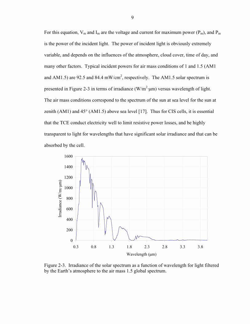
For this equation, Vm and Im are the voltage and current for maximum power (Pm), and Pin
is the power of the incident light. The power of incident light is obviously extremely
variable, and depends on the influences of the atmosphere, cloud cover, time of day, and
many other factors. Typical incident powers for air mass conditions of 1 and 1.5 (AM1
and AM1.5) are 92.5 and 84.4 mW/cm2, respectively. The AM1.5 solar spectrum is
presented in Figure 2-3 in terms of irradiance (W/m2·µm) versus wavelength of light.
The air mass conditions correspond to the spectrum of the sun at sea level for the sun at
zenith (AM1) and 45° (AM1.5) above sea level [17]. Thus for CIS cells, it is essential
that the TCE conduct electricity well to limit resistive power losses, and be highly
transparent to light for wavelengths that have significant solar irradiance and that can be
absorbed by the cell.
0
200
400
600
800
1000
1200
1400
1600
0.3 0.8 1.3 1.8 2.3 2.8 3.3 3.8
Wavelength (µm)
Irra
dian
ce (
W/m
2·µm
)
Figure 2-3. Irradiance of the solar spectrum as a function of wavelength for light filteredby the Earth’s atmosphere to the air mass 1.5 global spectrum.

10
The maximum power delivered by the cell is determined by the fill factor (FF) for
a solar cell. The fill factor is a measure of the squareness of the illuminated I-V curve,
and like efficiency is used to characterize all types of solar cells. A plot of a typical I-V
curve is presented in Figure 2-4 [18], where the hatched square represents the area of a
square defined by the product of Vm and Im, which equals Pm. The fill factor represents
the ratio of the maximum power square to the power square defined by Voc and Isc, where
Voc is the open circuit voltage, and Isc is the short circuit current. These relationships
yield Equations 2.2 and 2.3 [17].
FFV I
V Im m
oc sc
= (2.2)
η = ⋅FF V I
Poc sc
in
(2.3)
Figure 2-4. Theoretical plot of the I-V characteristics for a typical Si solar cell, with themaximum power rectangle highlighted [18].

11
The ZnO TCE primarily affects cell efficiency by influencing the FF and Isc. The role of
the TCE and the mechanisms for its influence on FF and Isc are discussed in Section 2.2.4
below, after coverage of basic concepts is completed.
To understand device physics, start with the simplest case of a p-n homojunction
diode formed near the surface of a bulk semiconductor wafer. A typical structure and
band diagram is shown schematically in Figure 2-5. In this device, there is a n-type
region on the surface, a depletion region containing the junction, and a p-type substrate.
If a photon with energy (Eph=hν) greater than the band gap (Eg) of the semiconductor is
absorbed, a valence band electron is promoted to the conduction band yielding an
electron-hole (e-h) pair. If this absorption process takes place in or within a diffusion
distance from the space charge or depletion region, the carriers can be separated by the
junction’s built-in potential (Vbi). The built-in potential is a function of the band bending
in the space charge region, and is therefore determined by the doping concentrations for a
homojunction [17].
Eg
hν>Eg
Ef
Ec
Ev
Vbi
Figure 2-5. Band diagram of a typical n-p homojunction solar cell, illustrating generationof an electron-hole pair by absorption of a photon.

12
Since the width of the depletion region is small relative to the thickness of the
cell, a significant portion of e-h pair generation occurs outside of the depletion region.
This region has no built electric field; therefore current transport only occurs due to the
diffusion field generated by the excess carriers. If these generated carriers reach the
depletion region, they contribute to power generation. If the carriers recombine before
reaching the depletion region, they do not contribute; therefore the minority carrier
lifetime and diffusion distance are critical to device performance [17].
2.2.3 Thin Film Solar Cells
Thin film solar cells are solar cells based on deposited thin films of
semiconductor materials, typically applied to inexpensive substrates (i.e., glass, polymer
films, and metal foils). The principle of using a semiconductor junction is the same, but
the structure and production of the cells are quite different. The device physics of thin
film cells are significantly more complicated than the idealized conditions described
above [3,4]. The solar cell structure presented in Figure 2-1 is a typical CIS based thin
film solar cell, and is comprised of several layers, the functions of which will be
discussed subsequently. Factors complicating the device physics arise from large defect
concentrations in the deposited films, and the necessity of using multiple layers.
Microstructural defects include point defects, dislocations, and extended defects such as
grain boundaries. Macroscopic defects include porosity/voids, pinholes, delamination,
and cracking. These defects lower the efficiency of the cell by degrading optical and
electrical properties. Multiple layers can hamper performance due to interfacial
recombination, potential barriers resulting from poor band alignment, and processing
constraints imposed by the different materials. Thus, compared to ideal cells, which are

13
most closely approximated by bulk single crystal devices, thin film devices are less
efficient.
Enthusiasm for thin film cells is maintained despite compromises in efficiency
because of the potential for substantially reduced production costs [3]. Costs are lowered
in source materials due to the relatively small volume of semiconductor material needed
to form thin films in contrast to bulk cells where the entire structure is semiconducting
material. This is an important advantage if a significant portion of the world’s power is
to be produced by solar cells. The area of cells needed to produce a significant fraction
of the world’s power demand is huge; therefore low material usage per unit area is
absolutely critical. A second advantage results from lower processing costs associated
with thin film devices versus bulk devices. As seen previously (Figure 2-2), tremendous
strides have been in made improving the efficiency of thin film devices, but high volume
production costs still need to be much lower to encourage widespread adoption of thin
film solar cells. In all cases, production costs are lower than high efficiency single
crystal devices, and compete with bulk poly-crystalline devices. Amorphous silicon
(a-Si) is still the cheapest solar cell material to produce, but continues to suffer from low
efficiency and lack of stability under long term illumination [4]. Amorphous silicon cells
are widely used in consumer electronic applications where power consumption is
minimal and low cost is critical (i.e., solar powered calculators).
The CIS material system has several advantages over other materials systems, one
being a large absorbance (α≈105 cm-1), which is larger than many other direct band gap
semiconductors [3]. The absorbance describes the ability of a material to absorb light as
expressed in Equation 2.4 where

14
I I e x= −0
α . (2.4)
The term I is the intensity of transmitted light, I0 is incident light, α is the absorbance
with units of cm-1, and x is the distance traveled through the absorbing medium in units
of cm. The high absorbance of CIS results in light being absorbed near the surface of the
film, and therefore in close proximity to a shallow p-n junction region. This also means
that the overall device can be thinner than a device based on a semiconductor with a
lower α. Another benefit is the band gap of the device can be controlled by introducing
Ga for In and S for Se, to match the band gap of the cell for most efficient utilization of
the solar spectrum and to form graded gap structures. Turning to the individual layers of
the CIS based solar cell in Figure 2-1, the substrate for thin film CIS solar cells is
inexpensive soda-lime (window) glass. A 1 µm thick film of molybdenum is sputter
deposited onto the glass substrate, and acts as a reflective back electrode to the solar cell.
The primary purpose of the Mo contact is to efficiently conduct electricity generated in
the CIS layer to the external circuit. The CIS layer is the semiconductor layer responsible
for absorbing the light, and is known as the absorber layer. The CIS layer is typically ~3
µm thick, and is deposited by a wide variety of techniques, of which co-evaporation has
achieved the best results (η=18.8%) [2]. Co-evaporation involves simultaneous
evaporation of Cu, In, and Se from elemental sources, and therefore requires
sophisticated flux controls to achieve proper stoichiometry. There is still considerable
debate as to whether the semiconductor junction formed in CIS based solar cells is a
homojunction within CIS, or a heterojunction formed with the subsequent CdS layer.
From the illustration of the cell in Figure 2-1, the layer on top of CIS is a very thin (50
nm) layer of CdS known as the buffer layer that is deposited by chemical bath deposition
15
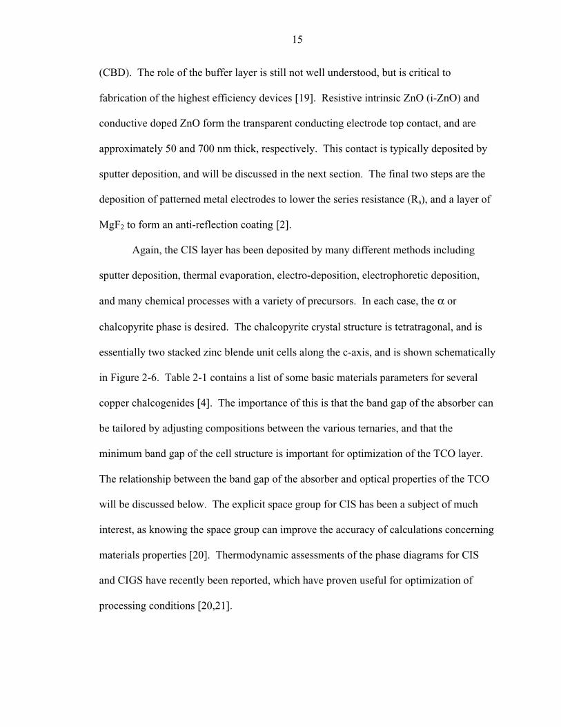
(CBD). The role of the buffer layer is still not well understood, but is critical to
fabrication of the highest efficiency devices [19]. Resistive intrinsic ZnO (i-ZnO) and
conductive doped ZnO form the transparent conducting electrode top contact, and are
approximately 50 and 700 nm thick, respectively. This contact is typically deposited by
sputter deposition, and will be discussed in the next section. The final two steps are the
deposition of patterned metal electrodes to lower the series resistance (Rs), and a layer of
MgF2 to form an anti-reflection coating [2].
Again, the CIS layer has been deposited by many different methods including
sputter deposition, thermal evaporation, electro-deposition, electrophoretic deposition,
and many chemical processes with a variety of precursors. In each case, the α or
chalcopyrite phase is desired. The chalcopyrite crystal structure is tetratragonal, and is
essentially two stacked zinc blende unit cells along the c-axis, and is shown schematically
in Figure 2-6. Table 2-1 contains a list of some basic materials parameters for several
copper chalcogenides [4]. The importance of this is that the band gap of the absorber can
be tailored by adjusting compositions between the various ternaries, and that the
minimum band gap of the cell structure is important for optimization of the TCO layer.
The relationship between the band gap of the absorber and optical properties of the TCO
will be discussed below. The explicit space group for CIS has been a subject of much
interest, as knowing the space group can improve the accuracy of calculations concerning
materials properties [20]. Thermodynamic assessments of the phase diagrams for CIS
and CIGS have recently been reported, which have proven useful for optimization of
processing conditions [20,21].

16
Figure 2-6. One unit cell of the CuInSe2 chalcopyrite crystal structure [20].
Table 2-1. Materials parameters for chalcopyrite ternary compositions.Compound a (Å) c/a Eg (eV)CuInSe2 5.782 2.0097 1.04CuGaSe2 5.596 1.966 1.68CuInS2 5.52 2.016 1.43CuGaS2 5.35 1.959 2.43
The CdS buffer layer is still an active area of research. Research is focused on the
role of the layer, since the most efficient devices have this layer. A large amount of
effort has addressed how to replace the CdS layer because of the toxicity of cadmium
[19]. The leading hypotheses regarding the role of the buffer layer are that it protects the
absorber layer from ion bombardment during the sputter deposition of ZnO, that the CBD

17
chemistry treats the surface in such a way that the interfacial electrical properties are
improved, and/or that it forms a high quality heterojunction. Some of the investigated
alternatives include In(OH,S), CdZnS, ZnS, and ZnO [19,22].
2.2.4 Transparent Conducting Electrode (TCE)
For bulk single crystal p-n junction based solar cells, the top layer of the cell
structure is typically a heavily doped n-type region. Therefore the resistivity of the
absorber material is low, and it can effectively conduct power to the metal grid, which
transfers the power to an external load. For the case of CIS based cells a fine grain size
and an inability to achieve a highly doped n-type region on the surface dictate the need
for an additional layer to efficiently conduct electricity. As this layer is on the top of the
cell, it must also transmit the useful portion of the solar spectrum. These needs are well
met by transparent conducting oxides (TCOs), of which ZnO has been found to be a
particularly good match for CIS based cells. The two primary mechanisms by which the
TCE affects the performance of the solar cell are through the fill factor (FF) and the short
circuit current (Isc).
There are several design constraints that make ZnO more attractive than other
TCOs for application to CIS based solar cells. One of the most fundamental is the
previously mentioned natural abundance and low cost of Zn. Also important is the
thermal budget available for this processing step. It is generally accepted that for the
current state of the art structures, processing above 200°C for any step after deposition of
CdS results in severe degradation of the cell’s performance [23]. Thus a high quality
TCO must be deposited at or near room temperature. Transparent conductors based on
ZnO have achieved resistivities in the low 10-4 Ω·cm by sputter deposition at room
temperature. Films of ZnO can also have greater than 90% transmittance in the visible

18
spectrum, which is one of the best values for TCOs, while maintaining good electrical
properties [24]. Also, as shown in Figure 2-7, the conduction band alignment between
ZnO and the underlayers is good [25], which is important for transport of conduction
band electrons generated in the absorber to the external load. In the presented schematic
band alignment diagram, the conduction band for ZnO is 0.4 eV and 0.1 eV below the
conduction bands of CdS and CIS, respectively. Additionally, ZnO is based on column II
and VI elements from the periodic table, as is CdS; therefore Zn and O are isoelectronic
in CdS.
As mentioned, the TCE influences the FF and Isc of the cell. For the case of FF,
the TCE can be a primary component of the series resistance (Rs), which can be seen in
Figure 2-7. Conduction and valence band alignments of a typically CIS based solar cellbetween the different layers of the structure [25].

19
the schematic equivalent circuit shown in Figure 2-8 [17]. Equation 2.5 was developed to
evaluate resistive effects in thin film solar cells [26].
FF FF CIR
V
V
V
V
I R
V
VS
F V F
S F Vscs
oc
m
oc
m
sc sh
m
ocI
m
I m
= − − −− ( ) ( )[ ]
+ ( )
0
2 2
2 2
1 0/
µ (2.5)
The term FF0 is the ideal diode fill factor and C is a parameter that is weakly dependent
on Voc/kT. The bracketed term on the right is a correction used for CdTe based solar
cells, and is therefore not applicable to CIS based solar cells. As can be seen, a high
series resistance and/or a low shunt resistance (Rsh) degrades the fill factor of the solar
cell. Shunt resistance is a term for the internal resistance of the solar cell, and therefore
controls the amount of power dissipated within the cell. A lower fill factor results in
decreased conversion efficiency. This point is well illustrated in the plots shown in
Figures 2-9(a-b) [18]. Figure 2-9a is a plot of four calculated I-V curves for an
illuminated solar cell with the permutations of Rs values of 0 and 5 Ω and Rsh values of
100 and ∞ Ω. While shunt resistance (Rsh) has minimal impact on the I-V curves, higher
series resistance (Rs) strongly decreases the cell’s fill factor. Figure 2-9b plots the
relative power generated versus Rs, and indicates the relative power (efficiency) drops
Figure 2-8. Equivalent circuit diagram for a solar cell, showing photocurrent (IL), darkcurrent (ID), series resistance (Rs), shunt resistance (Rsh), and a load (RL) [17].

20
(a)
(b)
Figures 2-9(a-b). Influence of a solar cell’s series resistance on the (a) fill factor asshown by the squareness of the I-V curve and (b) relative power as a function of seriesresistance [18].

21
sharply with increasing Rs, particularly between 0 and 4 Ω. Series resistance for state of
the art CIS based solar cells are ~0.2 Ω·cm2 [2], and improvement of this value by
decreasing the resistivity of the TCO layer will improve FF, and therefore efficiency of
the cell.
The second mechanism by which ZnO influences CIS based solar cells is optical
losses. This mechanism impacts the Isc, since photons absorbed in the TCE do not
generate photo-current. As will be detailed below, the optical properties and the
electrical properties are fundamentally related by the plasma resonance and band gap
energy, and are discussed in the section concerning optical properties of TCOs below.
Optical absorption is a function of the film’s thickness (x) and absorbance (α) as shown
in Equation 2.4. The series resistance is a function of thickness as well as the resistivity.
If the resistivity of ZnO is decreased, thinner films can be used resulting in less optical
absorption. The effects of light absorption in the TCE can be investigated by
spectrophotometry to characterize transmittance, and the spectral response of the cell,
which characterizes the quantum efficiency (QE). Dips in the efficiency for particular
wavelength regions of the spectrum can be correlated to spectrophotometry data from the
TCE to assess its impact on the solar cell.
2.3 Transparent Conducting Oxides
2.3.1 Background
Transparent conducting oxides (TCOs) have been investigated since the 1950s for
use in a variety of applications. Over these years, a large amount of research has been
done to improve the optical and electrical properties, and there are several excellent
reviews of the work that has been done on TCOs in general [11,12,27], and ZnO

22
specifically [28]. As a general class of materials, transparent conducting oxides (TCOs)
are made of binary and more recently multi-component metal oxides. They are applied
as thin films using various deposition techniques such as spray pyrolysis, sputter
deposition, chemical vapor deposition, molecular beam epitaxy, and laser ablation [28-
32]. The transparency is derived from a large band gap (Eg>3 eV), which prevents
absorption of visible wavelengths, and a lack of d-d transitions in the metal cations which
could act as color centers. The d-d transitions cannot occur if the d orbitals of the metal
cation are full, and therefore many TCOs incorporate this type of cations [13]. This
yields a transmittance in the visible often greater than 90% (T>90%). The low electrical
resistivity (ρ~10-3–10-4 Ω·cm) of these materials is derived from extremely high carrier
concentrations (n~1020-1021 cm–3), since the carrier mobilities are low (µ~5-50 cm2/V⋅s).
The low mobility is a result of both the inherently low mobility of the oxide materials,
and an array of scattering defects in the deposited films. Various figures of merit (FOMs)
that incorporate optical absorption and electrical conductivity have been proposed, but no
consensus has been reached on a universal FOM. Therefore FOMs are not commonly
used in the literature. Until very recently, useful conductivities could only be achieved
for n-type materials. This has changed with development of as p-type TCO materials
over the past few years [13].
The first oxide found to be transparent and conductive, CdO, was discovered by
Badeker in 1907 [33]. The first TCO useful for practical applications was indium oxide
doped with tin commonly known as indium tin oxide (ITO), which has a composition of
(In2O3:SnO2) (90wt%:10wt%). It was developed in the early 50s, and maintains some of
the best performance characteristics for optical transparency and electrical conductivity

23
[11,24]. It has been the TCO of choice during the last 50 years for applications
demanding the best conductivity with good optical properties in the visible regime.
Currently half of the indium produced in the world finds application in ITO for flat panel
display applications [34]. Other TCO materials that have received substantial attention
include tin oxide (SnO2) commonly doped with fluorine, and cadmium stannate
(Cd2SnO4), which is intrinsically doped. Table 2-2 is a list of historically significant
innovations in the TCO field with references compiled by Gordon [24].
Table 2-2. History of processes for making transparent conductors.Material Process ReferenceAg by chemical-bath deposition Unknown VenetianSnO2:Sb by spray pyrolysis J. M. Mochel (Corning), 1947 [35]SnO2:Cl by spray pyrolysis H. A. McMaster (Libbey-Owens-Ford), 1947 [36]SnO2:F by spray pyrolysis W. O. Lytle and A. E. June (PPG), 1951 [37]In2O3:Sn by spray pyrolysis J. M. Mochel (Corning), 1951 [38]In2O3: by Sputter Deposition L. Holland and G. Siddall, 1955 [39]SnO2:Sb by CVD H. F. Dates and J. K. Davis (Corning), 1967 [40]Cd2SnO4 by Sputter Deposition A. J. Nozik (American Cyanamid), 1974 [41]Cd2SnO4 by Spray Pyrolysis A. J. Nozik (American Cyanamid), 1976 [42]SnO2:F by CVD R. G. Gordon (Harvard), 1979 [43]TiN by CVD S. R. Kurtz and R. G. Gordon (Harvard), 1986 [44]ZnO:In by Spray Pyrolysis S. Major et al. (Indian Ist. Tech), 1984 [45]ZnO:Al by Sputter Deposition T. Minami et al. (Kanazawa), 1984 [46]ZnO:In by Sputtering S. N. Qiu et al. (McGill), 1987 [47]ZnO:B by CVD P. S. Vijayakumar et al. (Arco Solar), 1988 [48]ZnO:Ga by Sputter Deposition B. H. Choi et al. (KAIST), 1990 [49]ZnO:F by CVD J. Hu and R. G. Gordon (Harvard), 1991 [50]ZnO:Al by CVD J. Hu and R. G. Gordon (Harvard), 1992 [51]ZnO:Ga by CVD J. Hu and R. G. Gordon (Harvard), 1992 [52]ZnO:In by CVD J. Hu and R. G. Gordon (Harvard), 1993 [53]Zn2SnO4 by Sputter Deposition H. Enoki et al. (Tohoku), 1992 [54]ZnSnO3 by Sputter Deposition T. Minami et al. (Kanazawa), 1994 [55]Cd2SnO4 by Pulsed Laser Dep. J. M. McGraw et al. (CO. Sch. Mines & NREL),
1995 [56]

24
Focusing on development of ZnO as a TCO, research started in the late 1970s,
with major contributions starting in the 80s. Research in the early 80s focused on
intrinsically doped ZnO thin films [57,58], but the electrical properties of these films
were found to be unstable above 150°C [59]. The stability issue was resolved by using
extrinsically doped films. Figure 2-10 shows progress in decreasing the resistivity of
several TCO materials including ZnO with time. Table 2-3 presents a compiled list of
electrical properties for doped ZnO films deposited by magnetron sputter deposition.
From the table the reader can note that while excellent electrical properties have been
achieved, they involve either elevated substrate temperatures or positioning the substrate
perpendicular to the source. Recall that elevated temperatures are incompatible with
solar cell deposition process, and utilizing a substrate perpendicular to the source has
issues with uniformity and feasibility particularly with large area substrates. The low
Figure 2-10. Decreasing resistivity of transparent conducting oxides indicating improvedperformance as a function of time [60].

25
resistivities achieved suggest that there is room for improvement for films deposited at
room temperature with a parallel source and substrate geometry. Room temperature
deposition with a parallel substrate and source is most compatible with volume
production of CIS based solar cells, and therefore improving electrical properties
achieved by this process is critical to improved efficiency in production devices.
Table 2-3. Compilation of electrical data for sputter deposited ZnO thin films withseveral different dopants.Dopant Target ρ (x10-4)
(Ω·cm)n (x1020)(cm-3)
µ(cm2/V·s)
Reference
Al Zn:Al 4.2 2.6 57 Jäger et al. [61]Al Zn:Al 4.0 4.9 32 Jäger et al. [61]Al ZnO:Al2O3 7.7 4.2 19.5 Menner et al. [62]Ga ZnO:Ga2O3 5.9 5.9 20 Menner et al. [62]Al ZnO:Al 6.5 6.5 15 Cebulla et al. [63]Al ZnO:Al 14 4.0 10 Cebulla et al. [63]Al ZnAl 2.7 8.4 28 Kluth et al. [64]Al ZnO:Al2O3 1.9 11 30 Tominaga et al. [65]Al ZnO:Al2O3 4.7 7.5 15 Park et al. [66]Al ZnO:Al2O3 2.8 5.8 39 Löffl et al. [67]Al ZnO:Al 4.5 8.0 17 Ellmer et al. [68]Al ZnO:Al2O3 3.6 5.6 37 Nakada et al. [69]B ZnO + B2H6 4.0 2.6 60 Nakada et al. [69]B and Al ZnO:AlB12 6.5 2.4 40 Nakada et al. [69]Al ZnAl 2.7 4.3 53 Schäffler et al. [70]Al ZnO:Al 5.3 5.6 20 Konishi et al. [71]Al ZnAl 2.5 7.0 36 Mauch et al. [72]Al ZnAl 5.0 Harding et al. [72]In ZnIn 14 Igasaki et al. [73]Al ZnO:Al2O3 1.4 13 34 Choi et al. [49]Ga ZnO:Ga2O3 5.9 15 7 Jin et al. [74]Al ZnO:Al 5.4 4.5 26 Minami et al. [75]Si ZnO:SiO2 3.9 Minami et al. [75]In ZnO:In2O3 3.0 Qiu et al. [47]Al ZnO:Al2O3 1.9 15 22 Minami et al. [76]B ZnO:B2O3 6.4 2.5 39 Minami et al. [76]Ga ZnO:Ga2O3 5.1 4.4 28 Minami et al. [76]In ZnO:In2O3 8.1 4.0 20 Minami et al. [76]Defects ZnO (Ar+H2) 20 2.0 16 Webb et al. [77]

26
Transparent conducting oxide thin films are used for a variety of applications, and
depend on several different materials for optimum properties. The largest application is
for heat reflecting, low emissivity coatings for architectural glass. This application does
not require good electrical properties, only a high carrier concentration to achieve low
emissivity in the infrared. Due to the huge area of coated material, it also depends on the
use of an abundant and cheap material, which is easy to deposit. These criteria are best
satisfied by flourine doped tin oxide (SnO2:F) deposited by spray pyrolysis or chemical
vapor deposition [11,34]. Another large application is in visual displays. Modern
cathode ray tube (CRT) displays use TCO films to dissipate static, and absorb magnetic
radiation [34]. The flat panel display (FPD) industry uses TCO films as a transparent
contact for displays based on LCD, electroluminescent, plasma, and other technologies.
This application demands low resistivies (1-3x10⁻⁴ Ω·cm) and high transmittance
(T>90%) in the visible, but the optical properties in the IR are not critical [34]. The high
costs associated with FPDs make the expense associated with ITO justifiable for the
performance needed.
The application of interest for this work is the use of ZnO films for CIS based
solar cells. A solar cell TCE is a very demanding application, particularly for large area
modules because current is transported over long distances. Both a low resistivity and
high transmission in the visible and near infrared are critical to the efficiency of the
device. Also, in the band diagram presented in Figure 2-7, the electron affinity match
between ZnO and CIS is excellent, promoting good interfacial electrical properties. Zinc
oxide based TCE layers are also used for all the highest efficiency cells, indicating good
performance, and ZnO is inexpensive to produce due to the abundance of Zn, which is

27
critical to lowering production cost and enabling large volume production, respectively.
Additionally, the highly resistive i-ZnO layer is critical to formation of high performance
CIS based solar cells, and can be effectively deposited by adding oxygen to the sputtering
gas ambient with deposition of ZnO:Al. Therefore, ZnO is very suitable for application
as a TCE to CIS based solar cells.
2.3.2 Electrical Properties of TCOs
Improved electrical properties of deposited ZnO:Al thin films is one of the
primary objectives of this work; therefore, electrical properties of TCO materials are
reviewed and important concepts used to analyze results are presented. A majority of the
published literature discusses the electrical properties of TCOs in terms of resistivity (ρ),
which is the reciprocal of conductivity (σ), and has units of ohm·cm (Ω·cm). An early
difficulty arises in whether to treat the electrical properties using a metallic free electron
theory, or using semiconductor transport theory. Evidence that supports the case of
metallic conduction include the lack of temperature dependence for the carrier
concentration data down to very low temperatures (16K) [78]. This suggests that the
doping density has exceeded the Mott critical density [79], and therefore has metallic like
behavior. Above the Mott transition, the semiconductor is considered degenerate,
meaning that the wave functions of the dopant atoms are interacting. Thus, to obey
Pauli’s exclusion principle the defect level generated by the dopant splits and an impurity
band is formed. For the case of ZnO, at high doping levels, the impurity band moves into
the conduction band, and results in the Fermi energy (EF) being above the conduction
band edge. Above the Mott transition, the dopant atoms are no longer ionized, as there

28
are no free states to be thermally ionized into. This is consistent with the lack of carrier
freeze out behavior for low temperature Hall measurements [78].
The classical theory of conductivity in metals was developed by Drude at the turn
of the century, and is based on equations of motion for electrons, with a term for drag to
characterize the interaction of the medium with moving carriers. The conductivity, σ, or
inverse of resistivity (ρ-1) can be expressed as shown in Equation 2.6 [80,81].
σρ
τ= =1 2ne
m (2.6)
where n (cm-3) is the density of free carriers, e (C) is the charge of the electron, τ (s-1) is
the relaxation time for the carrier which relates time between collisions, and m is the free
electron mass. A relaxation time on the order of 10-15 seconds is typical for a TCO [82].
The term τ relates the motion of electrons to the applied electric field, as is shown in
Equation 2.7 [83], where νf is the final drift velocity for electrons and E is the electric
field strength.
τν
=m
eEf (2.7)
From this we can derive a mean free path (l) between carrier collisions, which is related
to the carrier velocity (ν) as shown in Equation 2.8 [83].
l = ντ (2.8)
Equation 2.8 is used in Chapters 5 and 6 to evaluate the mean free path for conduction
electrons. The carrier velocity (ν) used for these calculations is the thermal carrier
velocity, which is ~107 cm/s [83]. The term τ describes the interaction between the
electron and the material hosting conduction. The two fundamental mechanisms
controlling the relaxation time are scattering events with the lattice (phonon scattering)

29
and defect scattering. Phonon scattering is a function of temperature, and tends to
decrease with decreasing temperature. Defect scattering tends to be independent of
temperature. Because the different scattering mechanisms are independent of energy and
each other, the contributions of scattering by phonons, impurities, or defects can be
summed using Mathiessen’s rule as shown in Equation 2.9 [81].
ρ ρ ρ ρ= + +phonon impurity defect (2.9)
Metallic conductivity may also be described using quantum mechanics, with
similar results. The primary distinctions made by quantum mechanical description of
resistivity involves acknowledging that only electrons near the Fermi energy participate
in conduction, and that the drift velocity of the electron in an electric field is small
compared to the thermal velocity of the electrons at the Fermi energy. Therefore the
velocity in Equation 2.7 becomes the Fermi velocity (νF) instead of the drift velocity.
The vast majority of the literature treats TCOs as a degenerate semiconducting
material, and use transport equations developed for semiconductors in analysis of the
electrical properties. For this case, the relaxation time becomes a function of energy, and
relaxation by different mechanisms are no longer necessarily independent of each other.
For carrier concentration, it must be recognized that there are two types of carriers,
electrons (n) and holes (p). For ZnO, the carrier type is electrons, and is therefore similar
to metals with the exception that defects and/or impurities generate the carriers. The
relaxation time becomes a mean relaxation time <τ>, and is replaced in the conductivity
equations by a mobility (µ with units of cm2/V·s) as shown in the basic equation of
conductivity for a semiconductor presented in Equation 2.10.
σρ
µ µ= = +( )1ne pen p (2.10)

30
where n is the concentration of electron carriers (cm-3), p is the concentration of hole
carriers (cm-3), e is the charge of an electron, µn is the mobility of electrons (cm2/V·s),
and µp is the mobility of holes (cm2/V·s). Mobility describes the interactions between
carriers and the material through which they move. Carrier concentration is the density
of mobile charge carriers available for conduction. The relationship between the mobility
and the mean relaxation time is seen in Equation 2.11 [17],
µ τ= e
m* (2.11)
where m* is the effective mass, and <τ> is the mean relaxation time. For metallic
conduction, <τ> simplifies to τ, and shows that the mobility can remain a useful indicator
of carrier transport for metallic conduction [17]. Equation 2.11 is used to approximate
the carrier relaxation time from the Hall mobility.
The effective mass of an electron appears in Equation 2.11, and is a concept that
relates the influence of a material on the motions of electrons resulting from applied
forces (electric field, magnetic field, etc). If the relaxation time (τ) is constant, then by
Equation 2.11, a smaller effective mass will result in a larger mobility. As a general class
of materials, TCOs have large effective masses, which for ZnO is reported to be 0.27m0,
or 27% of the free electron mass [84].
Ideal ZnO, with perfect stoichiometry and no defects should be an insulator, with
resistivity greater than 105 Ω·cm. In reality, point defects are electrically active in ZnO,
and in particular Zn interstitials and/or O vacancies are typically believed to generate
conduction band electrons [85] which lower the resistivity to ~10-4 Ω·cm [86]. To lower
the resistivity to the 10-4 Ω·cm level desired for TCOs requires doping ZnO to carrier
concentrations above 1020 cm-3, while maintaining mobilities greater than 10 cm2/V·s.

31
ZnO is almost exclusively n-type and this is the case treated here. As a side note, p-type
ZnO has been recently reported, but has proven difficult to reproduce [13].
Doping can be accomplished by intrinsic and extrinsic dopants. Intrinsic dopants
result from deviations in stoichiometry, and are the source for the native n-type
conductivity that ZnO can have. In terms of Kröger-Vink notation, the native doping
defects are Zni and VO for zinc interstitials and oxygen vacancies, respectively. Intrinsic
doping can achieve carrier concentrations of low 1020 cm-3, and some of the best
mobilities (>50 cm2/V·s), with resistivities on the order of 10-3 Ω·cm [58]. The
drawbacks of intrinsic doping are the susceptibility to decreased carrier concentration
with increased temperature and oxygen potential of the gas ambient [59], inability to
produce sufficiently high carrier concentrations (n>5x1020 cm-3), and difficulty in
precisely controlling the stoichiometry to achieve the doping goals.
In the mid-80s, the use of extrinsic dopants was developed, allowing much of the
progress in decreasing resistivity shown earlier in Figure 2-10. Some of the most
commonly used dopants are group III elements, which substitute on the Zn lattice and act
as electron donors [60]. The most commonly used dopant is Al, but B, Ga, and In have
also been used. The group III element contributes one carrier per atom to the conduction
band. Aluminum is abundant, easily incorporated, cheap, and non-toxic. A halogen atom
on the oxygen also acts as a donor, contributing one electron to the conduction band.
Fluorine (FO) is the only halogen reported in the literature, and substitutes well for O
because of their similar ionic radii [86]. Resistivity, carrier concentration, and Hall
mobility of 4x10⁻⁴ Ω·cm, 5x1020 cm-3, and 40 cm2/V·s have been reported [50]. The high
mobility is hypothesized to result from F sitting on the O sublattice, where the ionized F-

32
impurity scattering center introduced by the dopant primarily affects the valence band,
and therefore does not as effectively scatter carriers in the conduction band [50]. On the
other hand, group IV elements, and a variety of transition metals have been shown to
exhibit poorer electrical and optical properties than the group III elements and F [60],
presumably due to increased scattering. One difficulty in controlling carrier concentration
is that intrinsic and extrinsic doping mechanisms can both be active. Recall that intrinsic
doping results from deviations in stoichiometry in the form of Zni and VO. Typically
atomic densities are 5x10²² atoms/cm3, while typical doping levels are 1020 cm-3,
indicating stoichiometric changes of ~0.1% can yield significant changes in carrier
concentration. Additionally, the native defects of oxygen interstitials (Oi) and zinc
vacancies (VZn) are reported to compensate conduction band electrons [85], and can
therefore decrease carrier concentrations generated by intrinsic and/or extrinsic doping.
Grain boundaries add an additional layer of complexity to the investigation of
electrical properties. Surface states and chemisorbed oxygen species both deplete carriers
from the conduction band [9,78]. Surface states are states formed within the band gap
resulting from the break in atomic bonding symmetry at the interface. Carriers enter the
deep levels, and a space charge region occurs on each side of the grain boundary as
shown in Figure 2-11 [3]. Similar to a p-n junction, the width of this depletion region is a
function of the carrier concentration, and becomes smaller as the carrier concentration
increases [78]. As the potential barrier becomes very narrow, tunneling transport
supercedes thermionic associated with the Petritz model for grain boundary scattering
[87]. The influence of grain boundaries on the electrical properties occurs through
scattering, which is considered below.

33
Figure 2-11. Schematic representation of the influence of grain boundaries and interfacestates on the band bending at the interface [3].
The issue of chemisorbed oxygen species at grain boundaries is important for
applications of ZnO as a solid state gas sensor [6,9]. Changes between reducing and
oxidizing ambients can be measured by changes in the resistivity of the material. In an
oxidizing ambient, oxygen species, often attributed to O-, bond to the surface by trapping
a conduction band electron from ZnO. When the surface concentration of the species is
high, and the grain size of ZnO is small, the grains can become depleted of carriers, and
result in a significant increase in the resistivity. A schematic of the chemisorption
process and its influence on band bending at the grain boundaries is presented in Figure
2-12 [9]. Though this illustration uses SnO2, ZnO follows the same process. It shows
two grains of SnO2 with chemisorbed oxygen. Below is a schematic of the potential
across the grain boundary, and illustrates how the potential barrier is smaller when

34
Figure 2-12. Illustration of the chemisorbed oxygen mechanism for solid state gassensors, and the influence of chemisorbed oxygen on band bending at interfaces [9].
the sensor is in reducing environments, and higher in oxidizing environments. If a ZnO
sensor is held at an appropriate temperature, and placed in a reducing gas, the
concentration of the surface oxide species decreases, and the resistivity decreases. The
decrease in carrier concentration resulting from the chemisorption process affects the
electrical properties in two ways. The first is the lowering of the carrier concentration,
which directly lowers the conductivity. Secondly, increased chemisorption results in a
wider potential barrier, which more effectively scatters carriers, and therefore decreases
carrier mobility [6].
A high carrier concentration is critical for a good TCO, but there are certain
fundamental limits that must be addressed. The carrier concentration has a direct
influence on the optical properties of the material. This relationship will be explored in
the following section regarding the optical properties of TCOs. The end result is that a

35
very high carrier concentration compromises the optical properties of the material. These
limits on high carrier concentrations result in carrier mobility being an important
parameter for reducing the deposited film’s resistivity. Increased mobility yields small
improvements to optical properties in the infrared. Therefore to lower the resistivity, it is
critical to increase the carrier mobility or identically lengthen the carrier relaxation time
[11,82].
As was shown in Equation 2.11, the mobility is a function of the effective mass of
the carriers, and the mean time between collisions. The effective mass is an intrinsic
property of the material, which is m*=0.27 for the case of pure ZnO. Therefore in order
to increase the mobility, the mean time between carrier scattering events must be
lengthened. Scattering involves the interaction of carriers with various aspects of the
material, with important scattering mechanisms in TCOs including the crystalline lattice
(µa), ionized impurities (µi), neutral impurities (µ n), and grain boundaries (µg). Equation
2.12 is used to sum the effects of multiple scattering mechanisms.
1 1 1 1µ µ µ µ
= + + +i a g
K (2.12)
If one scattering mechanism is the culprit for a significantly lower mobility, then the
overall mobility tends to be near the lowest value, and the scattering mechanism with the
lowest mobility is considered the dominant scattering mechanism. If the carrier
mobilities from more than one scattering mechanism are similar then the overall mobility
will be lower than the individual components.
Lattice or phonon scattering occurs when charge carriers interact with lattice
vibrations, which for a material with more than one atom per primitive basis has optical
and acoustic phonon modes [17]. The only way to increase the mobility resulting from
36
phonon scattering is to decrease the temperature, which is not practical for TCO
applications. Therefore, this scattering mechanism is relatively fundamental, as this form
of scattering occurs even in a perfect crystal. The limiting value for mobility due to
phonon scattering in lightly doped (n~1016 cm-3) single crystalline ZnO is approximately
µa=250 cm2/V·s [88] at room temperature. For both metallic and semiconductor
conduction, phonon scattering is temperature dependent, with mobility increasing with
decreasing temperature [80].
Ionized impurity scattering involves interactions and scattering of charge carriers
by ions within the material through coulombic forces. This mechanism commonly
dominates the mobility of highly doped silicon semiconductors used in today’s integrated
circuits. It is also commonly cited as the dominant scattering mechanism in TCO
materials [60,78,89]. This mechanism, it is treated by a variety of different models and
assumptions, typically with little or none of the derivation provided in accessible peer
reviewed literature. Recall that the Mott transition describes the transition between
insulating and metallic character with doping for a semiconductor. If heavily doped ZnO
has made the transition to metallic character, then impurities are no longer ionized [79].
Temperature dependent Hall measurements taken from a variety of TCO materials
including ZnO show a constant carrier concentration to low temperatures (T<20K or
kT<2 meV ), which suggest metallic character. Even if they are not ionized, dopant
atoms could still yield scattering as neutral impurities, which will be discussed below.
Ionized impurity scattering is modeled as a coulombic potential between ionized
atoms and charge carriers, and analyzed using quantum mechanic methods. The Brooks-
Herring model adds a screening potential due to other carriers [90]. Higher

37
concentrations of ionized impurities yield more interactions, and therefore a lower
mobility. For the non-degenerate case, the mobility due to ionized impurity scattering
increases with temperature. Equation 2.13 gives the relationship between the mobility
from ionized impurity scattering, temperature, and the ionized impurity density (Ni) [17].
µii
T
N∝
3
2
(2.13)
This relationship is based on use of the Maxwell-Boltzmann distribution function,
whereas the Fermi-Dirac distribution function should be used for a degenerately doped
semiconductor. In a report by Zhang et al., it is suggested that mobility from ionized
impurity scattering losses its dependence on temperature when the Fermi-Dirac
distribution function is used for the degenerate semiconductor case [78].
Neutral impurity scattering results from non-ionized point defects scattering
charge carriers [17]. For the case of semiconductors, this scattering mechanism is
typically only important at low temperatures when ionization of dopant atoms is frozen
out. In contrast, neutral impurities are a common scattering mechanism in metallic
conductivity. This is expected, as semiconductor materials tend to have exceptionally
high purity with most foreign atoms being purposely introduced to ionize and dope the
material. Neutral impurity scattering is a not a function of temperature, but is found to
vary with the density of neutral impurities [17]. Increasing concentrations of neutral
impurities decrease the mobility. For the case of metallic conduction, neutral impurities
are believed to scatter carriers by interrupting the periodicity of the lattice [80].
Two other sources of scattering are dislocations and extended defects such as
grain boundaries. For metallic conduction, these defects cause scattering by introducing

38
perturbations in the periodicity of the crystal structure. Like neutral impurities, as the
concentration of defects increases, more scattering occurs, which decreases the mobility.
The effect of dislocations on carrier transport in semiconductors models the dislocation as
a line charge in combination with a strain field [17]. This yields a mobility that is a
function of the density of dislocations (nd) and temperature, as shown in Equation 2.14
[17], where
µd
dn T
∝ 11
2
. (2.14)
The Petritz model is the most established theory for modeling carrier scattering at
grain boundaries [87]. This model specifies that surface states at the boundary yield a
depletion region around the boundary, and a potential barrier develops that must be
surmounted for transport, and therefore relies on thermionic transport [78]. For the case
of degenerately doped ZnO, the depletion region at the interface becomes very narrow,
increasing the probability of carriers tunneling through the potential barrier, which
decreases scattering [78]. This case is more analogous to metals, where grain boundary
scattering tends to be a small effect at room temperature.
Chemisorption of oxygen species further complicates modeling electrical
properties of grain boundaries. Recall that chemisorption of oxygen species trap
conduction band electrons, and therefore can cause a depletion region at grain
boundaries. The depletion region and the grain boundary can result in a potential barrier
similar to the potential barrier generated by interface states considered above. The
magnitude of changes in resistivity caused by chemisorption of oxygen species depends
on the carrier concentration, surface area/grain boundary area to grain volume ratio, and
concentration of chemisorbed oxygen species. For larger grain sizes in a heavily doped

39
material, the ratio of charge trapped in chemisorbed species to the quantity of carriers in
the grain is small, therefore chemisorption does not significantly increase resistivity. For
the case of very small grains or very thin films, chemisorption can trap a significant
portion the free carriers, which decreases carrier concentration, and increase grain
boundary scattering, and therefore increases resistivity. The sensitivity of resistivity for
ZnO thin films to the oxygen potential of the annealing ambient, even at mild
temperatures (300 – 400 °C) is widely attributed to this process [11,91,92]. It is difficult
to measure the amount of chemisorbed oxygen in as deposited films due to contamination
in the atmosphere for transfer of samples to characterization tools. If the quantity could
be investigated and controlled, improved film electrical properties could result.
2.3.3 Optical Properties
The optical properties for deposited ZnO films are of critical importance towards
application as a TCE, and are also useful for characterizing electrical properties of the
films. The optical properties of TCOs arise from the interaction of light with electrons,
and the physical structure of the film. The goal is to minimize these interactions, such
that transmission of light is maximized. Processes involving electrons include band edge
absorption [17], plasma resonance effects (absorption and reflection) [80-82], the
Burstein-Moss shift [93], and defect absorption. Processes based on the physical
structure of the film include thin film optical interference or Fabry-Perot oscillations [94],
and light scattering [95]. Each of these effects will be discussed below, along with their
influence on the optical properties of ZnO thin films.
Band edge absorption involves absorption of a photon to promote an electron
from the valence band to the conduction band of a semiconductor. This absorption only
occurs if the photon energy is greater than the band gap energy of the material. The band

40
gap of ZnO is direct and is about 3.2 eV for intrinsic material, which corresponds in
energy to a photon with a wavelength of 388 nm. Equation 2.15 shows the relationship
between absorbance (α), photon energy (hν), and the band gap energy (Eg) for allowed
direct transitions [17].
α ν= −( )K h Eg
1
2 (2.15)
The term K is a material dependent constant, and is independent of the photon energy.
This equation is useful for calculating the optical band gap of a material from
spectrophotometry data. As we can see from the AM1.5 solar spectrum in Figure 2-3, a
band gap of about ~3 eV (λ~400 nm) is the minimum band gap for transmitting most of
the solar spectrum.
The second optical effect that is critical for a TCO is plasma resonance effects.
The term plasma refers to mobile charge carriers, in the case of n-ZnO, electrons in the
conduction band. The carriers can be accelerated by the electric field component of
electro-magnetic radiation, and their motion can be modeled as Lorentzian Oscillators
[80,81]. The optical properties that result from these carriers were derived by Drude, and
involve using a combination of the classical wave equation for motion of the carriers and
Maxwell’s equations to determine the complex permittivity that results. The real (ε1) and
imaginary (ε2) components of the complex permittivity can be used to determine
reflection, absorption, and transmission characteristics of the electron plasma [80,81].
The results for TCOs are similar to those of metals, and show that the carriers can
resonate with the EM radiation at a particular frequency known as the plasma resonance
frequency (ωp). The plasma resonance frequency ωp is a function of the carrier

41
concentration, the effective mass of the electron, and the dc (ε0) and high frequency (ε∞)
dielectric constants as shown in Equation 2.16 [80-82].
ωε εp
ne
m=
∞
2
0
1
2
* (2.16)
This frequency is then used in equations for the complex permittivity, or complex
dielectric constant, which has a real component (ε1) and a complex component (ε2).
Relationships between the frequency of an electric field, the plasma resonance frequency
ωp, and the dielectric constant are shown in Equations 2.17 and 2.18.
ε εωω1
2
21= −
∞
p (2.17)
εε ωω τ2
2
3=
∞ p (2.18)
The term ω represents the angular frequency of the incident light, τ is the carrier
relaxation time, and ε∞ is the high frequency dielectric constant. The equations are based
on the assumption that 1/τ << ω [82], indicating that the carriers are free. The results of
these equations are that for ω<ωp, ε1<0 and ε2 is large which yields reflective behavior.
For the region near ω=ωp, ε1=0 and ε2 is smaller, yielding a transition region from
reflecting to absorbing character, which is seen in the plot of film reflectance versus
wavelength in Figure 2-13a [82], where the wavelength at which the transition occurs
changes with carrier concentration. Observe that higher carrier concentrations move the
transition associated with the plasma resonance frequency ωp to shorter wavelengths. In
Figure 2-13b [82], absorptance is plotted versus wavelength, and shows the effects of
carrier concentration on free carrier absorption. The absorptance relates the percentage
of the incident light that is absorbed by the film, and care should be taken not to confuse

42
it with absorbance (α) the intrinsic property of a material that defines its ability to absorb
light. The other term used in this work is absorption or optical absorption, which is the
product of the absorbance and the distance light travels through the medium (α·x), and is
a unitless number. Figure 2-13c [82] also plots absorptance versus wavelength, and
shows changes in absorptance with mobility. Notice that high carrier concentrations
increase absorptance, and moves the peak in absorptance to shorter wavelengths, while
increasing mobility decreases absorptance, but does not influence the wavelength of the
peak. As ω increases, ω>ωp, ε1 approaches ε∞, and ε2 approaches 0, yielding classic
dielectric behavior, which indicates EM radiation propagates through the material. This
behavior is seen in each of the above plots as the region where neither reflection nor
absorption occurs indicating light is transmitted.
The wavelength at which free carrier optical effects are significant are controlled
predominantly by the carrier concentration and carrier effective mass. For the case of
ZnO on a CIS based solar cell, the band gap of CIS is 1.04 eV, which corresponds to a
wavelength of ~1200 nm. ZnO with an effective mass m*=0.27 and a carrier
concentration of 5x1020 cm-3 has a plasma resonance frequency ωp which corresponds to
a wavelength of 1200 nm. Therefore the optical properties for samples with carrier
concentrations on the order of 5x1020 cm-3 and above must be measured to determine the
impact on the solar cell performance.
In contrast to carrier concentration, which if values are too large will result in the
deposited film reflecting or absorbing light needed by the cell, higher carrier mobilities
do not change the plasma resonance frequency. Recall that increasing mobility in fact
helps decrease the absorptance resulting from free carrier absorption. This indicates that

43
(a)
(b)
(c)
Figures 2-13(a-c). Theoretical plots of relationships between electrical and opticalproperties for (a) reflectance versus carrier concentration, (b) absorptance versus carrierconcentration, and (c) absorptance versus carrier mobility [82].

44
the mobility can be increased, which decreases resistivity, without compromising infrared
transmittance. Thus, decreasing the resistivity of ZnO for solar cell applications is best
accomplished by improving the mobility, while maintaining the maximum carrier
concentration not degrading infrared transmittance for wavelengths needed by the solar
cell.
The Burstein-Moss shift is a band gap widening process that can occur in
degenerately doped material [93]. As the carrier concentration increases, the Fermi
energy moves above the conduction band edge, resulting in complete occupation of states
at the bottom of the conduction band. Therefore, optically stimulated transitions to these
states cannot occur, and the optical band gap of the material increases. This process is
illustrated schematically in Figure 2-14. The vertical area shows the allowed transition
from the valence band to an energy in the conduction band above the Fermi energy. The
amount of the shift is a function of the doping concentration, and the density-of-states
effective mass (mcv*) as shown in Equation 2.19 [11].
∆Eh
m
ng
cv
=
22
3
83
* π (2.19)
The density-of-states effective mass reflects the fact that the effective mass of a
conduction band electron can be a function of conduction band density-of-states in some
situations [96]. For the particular case of ZnO, the band gap is already large enough that
the useful solar spectrum is transmitted effectively, so an increase in the band gap is not
required.
Defect absorption for TCOs can take two forms, absorption of light that promotes
an electron to a defect level, and absorption by metallic particles in the TCO. These

45
E
k
EF
ConductionBand
ValenceBand
E=hν
Figure 2-14. Illustration of the Burstein-Moss shift, which increases the optical band gapdue to occupancy of states in the conduction band.
processes will be discussed qualitatively. The first process involves an impurity or defect
of some form which generates a state within the band gap. A photon with the correct
energy can promote an electron from the valence band or another defect state into the
defect state, with the photon being absorbed. The second process arises because many
TCOs are intentionally or unintentionally off stoichiometry towards the oxygen deficient
side. If the material is far enough off stoichiometry, then highly reflective scattering
precipitates can form. This more often occurs in films deposited by reactive sputter
deposition, as seen by the transition from opaque to transparent films with increasing
oxygen partial pressure in the sputtering gas [97]. Poor transparency across the visible
spectrum is often attributed to defect absorption, but typically no mechanism for the
absorption is given.
The next two effects are based on the structure of the film and the fact that the
index of refraction (n) for pure ZnO is n=2.1 [94], which is different than glass (n=1.4)
and air (n=1.0). The result for films with a thickness on the order of the wavelength of
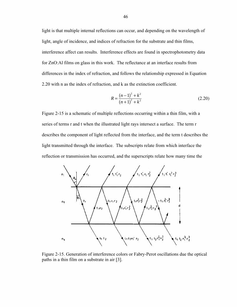
46
light is that multiple internal reflections can occur, and depending on the wavelength of
light, angle of incidence, and indices of refraction for the substrate and thin films,
interference affect can results. Interference effects are found in spectrophotometry data
for ZnO:Al films on glass in this work. The reflectance at an interface results from
differences in the index of refraction, and follows the relationship expressed in Equation
2.20 with n as the index of refraction, and k as the extinction coefficient.
Rn k
n k= −( ) +
+( ) +11
2 2
2 2 (2.20)
Figure 2-15 is a schematic of multiple reflections occurring within a thin film, with a
series of terms r and t when the illustrated light rays intersect a surface. The term r
describes the component of light reflected from the interface, and the term t describes the
light transmitted through the interface. The subscripts relate from which interface the
reflection or transmission has occurred, and the superscripts relate how many time the
Figure 2-15. Generation of interference colors or Fabry-Perot oscillations due the opticalpaths in a thin film on a substrate in air [3].

47
light ray has been transmitted or reflected from the interface. For the case of solar cells,
an anti-reflective coating (typically 1/4λ thick MgF2) is applied to the surface, which
prevents initial reflections from the ZnO. The Fabry-Perot oscillations result in an
oscillatory behavior in the transmittance and reflectance spectra, and can be see clearly in
most of the collected spectrophotometry data.
The final effect to consider is scattering of light. Scattering can occur at the
film’s surface, which typically results from roughness, or from within the bulk of the
film. Scattering from within the film results from inhomgeneity in the index of
refraction, which can result from extended defects such as grain boundaries, inclusions,
voids, cracks, and others [94]. The films produced in this work are highly transparent to
the eye, and specular reflection from the films surface is observed, suggesting that
minimal scattering is occurring from the surface or “bulk” of the film.
2.4 Sputter Deposition
2.4.1 Background
The primary focus of this work is on improving the properties of sputter deposited
ZnO:Al thin films. It is therefore critical to present some background knowledge about
sputter deposition, influences the various process parameters exert on the plasma, and
their relationship to properties of the deposited film. The sputtering process was first
report in 1852 by Grove [98]. It has evolved significantly since then to the point that in
the last 50 years it has been used to deposit films on architectural glass, integrated
circuits, hard drive platters, and a plethora of other applications. The sputtering process
is a glow discharge or a plasma process, which uses ionized gas atoms/molecules
accelerate in an electric field to erode material from a source (target), which then

48
condense from the gas phase on a work piece (substrate). A strong negative field is
applied to the target to attract positive ions, hence a sputter deposition source is referred
to as the cathode. If a thin film with the same chemistry as the target is desired, a noble
gas (e.g. Ar) ambient is typically used.
The erosion of the target is a momentum transfer process [99], the efficiency of
which is termed the sputter yield (S atoms/ion). Liberating a deposited flux involves
transferring energy to surface atoms of the target material, and the atoms of the surface
acquiring enough energy to escape the target. The maximum energy transferred between
two colliding particles is determined by the difference in their mass as shown in Equation
2.21 [94].
E
E
M M
M M2
1
1 2
1 2
24=+( ) cos θ (2.21)
The terms E1 and E2 refer to the energy of the separate particles in a binary collision, M1
and M2 are the masses of the particles, and θ is the angle of the collision. Equation 2.21
represents the maximum energy that can be transferred from the energetic gas atom
impinging on the target to a surface atom on the target. The energy needed to liberate an
atom from the target is related to its surface binding energy (Eb), and therefore this
minimum quantity of energy must be supplied by the ions to sputter the material.
Equation 2.22 [94,100] expresses the relationship between sputter yield (S) and energy
transfer from Equation 2.21, surface binding energy (Eb), kinetic energy of the ions (E1),
and a term describing the efficiency of transferred momentum between ions and surface
atoms (α).
SM M
M M
E
Eb
=+( )
34
42
1 2
1 2
21α
π (2.22)

49
Equation 2.22 is valid for ion energies E1<1000 eV, and one mass is taken to be the
sputtering ion and the other being the sputtered atoms mass. Sputtering yield is also
influence by the incident angle of the ions, as this influences the collision cascade the ion
undergoes within the target [101]. A factor that has been found to be critical in this
research is the distribution angle of the flux leaving the target. For each point on the
target that generates a deposited flux, the flux leaving that point source is a function of
the angle relative to the target’s normal axis. This is known as the cosine or power cosine
distribution, and is shown schematically in Figure 2-16 [102]. In Figure 2-16, as the
angle departs from the targets normal, the flux decreases following either a cosφ or cosnφ
relationship [102]. For sputter deposition, n is typically 0.5<n<2.0 [101]. The deposition
rate is a function of the sputter yield, the flux of ions impinging on the target, transport of
the deposited flux to the substrate, and sticking of that material to the substrate [94]. The
characteristics of the resulting film depend on the material, its mobility on the surface, the
geometry of the incoming flux, and the amount of energy imparted by species
bombarding the substrate.
Figure 2-16. Plot of the power cosine distribution, which controls the flux distribution asa function of angle relative to the targets normal [94].

50
For the case of DC sputter deposition, there are several source geometries in use,
one of which is the planar sputter deposition source. Two common varieties of planar
sources are diode and magnetron, and are illustrated in Figures 2-17a and 2-17b,
respectively. The name diode sputtering comes from the I-V characteristics of the plasma
which are similar to that of a diode, i.e. more current flows with forward bias versus very
little current flow with reverse bias. To achieve a sustainable plasma, the vacuum
chamber is initially evacuated to a pressure typically on the order of 10-8-10-6 Torr, to
achieve an ambient that will not contaminate the deposited film. Then the chamber is
back filled with the working gas to a pressure on the order of 1-200 mTorr, the range
needed to sustain the plasma. The sputtering pressure is an important parameter, since it
influences the resistance of the plasma, and therefore the I–V characteristics of the
plasma. As the pressure increases, the plasma becomes effectively less resistive, the
Target
PlanarDiode
Target
NSN
SNS
PlanarMagnetron
(a) (b)
Figure 2-17(a-b). Illustrations of planar sputter deposition sources in the (a) diodeconfiguration and (b) magnetron configuration.

51
voltage drops and the current increases. The current is related to the ion flux impinging
on the target, and the voltage is the bias of the target, which controls the velocity of the
impinging ions. The target geometry also influences the I-V characteristics of the
plasma. Increasing the target area yields a higher ion current for the same ion flux
(ions/cm2·s), effectively lowering the resistance of the plasma. Modern DC power
supplies can control the power, voltage, or the current of the discharge depending on
needs. The deposition rate typically scales linearly with deposition power [101].
One of the benefits of sputtering can be the relative high energy of the deposited
material [94,101] with values of 5 eV of kinetic energy compared to ~100 meV for
thermal deposition sources. The higher energy increases surface mobility of adatoms,
therefore allowing more rearrangement of atoms on the surface, typically yielding
improved film properties. By the kinetic theory of gases, an atom is more likely to be
inelastically scattered at higher gas pressures. This advantage is lost if the deposited
material loses energy in gas phase collisions during transport to the substrate. Scattering
in the gas phase also influences the flux of reflected neutrals that impinge on the
substrate. Reflected neutrals are ionized atoms/molecules that are accelerated towards
the target, and then neutralized and reflected from the target with a significant portion of
their incident energy. Their impact on the substrate can affect the microstructure and
residual stress in the deposited thin films. The substrate to target distance can also affect
the degree of gas phase scattering that occurs. As the distance the sputtered atoms travel
through the process ambient gas increases, more scattering occurs. Additionally, as the
target to substrate distance increases, the angular distribution of the flux causes the flux
to spread out in space, and therefore increasing distance decreases the deposition rate.

52
Another important parameter is the substrate temperature. This parameter is
important to adatom mobility, desorption processes, and thermodynamic driving forces
which affects phase stability and nucleation and growth phenomena. Thus the deposition
rate and microstructure of the developing film can be influenced by substrate
temperature. The influence of substrate temperature on the microstructure of deposited
film will be discussed more thoroughly in Section 2.4.2
Magnetron sputtering involves placing magnets behind the sputtering target. The
resulting magnetic field extends into the gas ambient in front of the source, and
influences the trajectories of moving charge particles by the Lorentz force [94]. The
result of this is confinement of electrons near the sputtering target, which increases the
amount of ionization in the working gas. Ions are not confined here because the charge
to mass ratio is much smaller, and therefore ion trajectories are not as strongly influence
by the magnetic field. The higher degree of ionization in the plasma effective lowers its
resistance, increasing the ion flux (current) relative to the target bias (voltage), and
effective increases the sputtering rate and broadens the operating pressure range. This is
desirable for a high rate process, which is useful for decreasing manufacturing costs.
Also, high deposition rates limit the exposure time of the growing film to the vacuum
ambient, and therefore helps lower the incorporation of gas phase contaminants into the
films [94].
The other major class of sputtering apparatus is radio frequency (RF) sputtering.
Similar to DC, RF sources can be diode or magnetron based. The planar target geometry
will be considered. Sputter deposition using RF power can be used to deposit material
from insulating targets. Power from a RF generator typically operating at 13.56 MHz is

53
transmitted to a matching network via a 50 Ω coaxial cable. The matching network
consists of a variable capacitor and inductor, and is needed to match the impedance of the
capacitive discharge plasma to the 50 Ω output impedance of the generator. The applied
RF field would normally tend to just oscillate charged particles, and therefore not
generate any sputter deposition. However, due to the large difference in mass between
ions and electrons, oscillations of the electrons are large enough that a significant portion
impinges on the target and the chamber, whereas the ions are basically static. Because
the chamber walls are grounded, and the target is electrically floated on capacitors, the
target tends to build up a negative charge over time, i.e. develops a negative bias. As the
negative bias increases, positive ions in the plasma become more strongly attracted to the
cathode and acts to increase the positive ion current. A steady state bias is achieved
when net current transported by positive ions and electrons in each full oscillation of the
electric field is zero. At these steady state conditions, a negative bias on the order of 100
to 1000 of Volts exists on the cathode, and is known as the cathode self bias. This bias is
sensitive to many parameters, including those mentioned above for the case of the I-V
characteristics of a DC discharge. Additionally, the bias is sensitive to the ratio of
capacitance for the target structure to the surrounding system. In practice this translates
to a target bias that can be highly sensitive to the system geometry [99]. Figure 2-18(a)
depicts what occurs when the RF power is initially applied to the target. Figure 2-18(b)
is for steady state the condition, and depicts the developed negative bias or target self bias
as seen by the voltage offset of the RF signal [103].

54
Figure 2-18(a-b). Illustration of the negative self bias formation during RF sputterdeposition with (a) power initially applied and a large excess electron current and (b) atsteady state where the electron current equals the positive ion current [99].
2.4.2 Thin Film Coalescence
Processes occurring at the substrate can also have a large influence on the
structure and properties of the sputter deposited films, and are therefore critical to
investigating relationships between the deposition process and resulting film properties.
Nucleation and growth of the deposited film will be discussed using capillarity theory
[94]. The processes involved are adsorption and desorption of material from the
substrate, and motions and reactions on the surface. Capillarity theory uses a
combination of bulk and surface free energies (surface tension) to assess the driving
forces participating in the nucleation and growth process. Figure 2-19 shows the balance
of surface tension forces involved with a nucleus on a substrate. The terms γsv, γvf, and γfs
represent surface tensions between surface-vapor, vapor-film, and film-surface,

55
Figure 2-19. Representation of the influences of surface forces on the morphology of adeposited film during nucleation based on the capillarity theory [94].
respectively, while θ is the contact angle between the substrate and the nucleus. The
angle θ changes to balance the surface tensions present. The degree to which the
adatoms respond to the forces exerted is related to their ability to move on the surface.
This surface mobility is related to the kinetic energy of the arriving adatom, energy
available to move the adatom (e.g. heat, ion bombardment), and the surface diffusivity of
the adatom [101]. The most common method to increase the mobility of adatoms is to
heat the substrate, but there are often constraints and trade-offs, which limit temperatures
in practice. For sputter deposition, recall that impingement of hyper-thermal atoms
(atoms with kinetic energy greater the kT) can increase motions of surface atoms, and
thereby influence the microstructure of the developing film.
For sputter deposition the working pressure and substrate temperature most
strongly influence the adatom mobility. Thornton developed a structural model relating
substrate pressure and temperature to the morphology of the film, and is known as a

56
Structural Zone Model (SZM). Figure 2-20 is a diagram of the SZM that Thornton
developed empirically by microstructural characterization of sputter deposited metal
films [104]. The four basic zones are 1, T, 2, and 3, with zone 1 occurring at higher
pressures and lower temperatures. Zone 1 is characterized by a columnar grain structure
with significant porosity between the grains, and large defect concentrations within the
grains. Films with a Zone T microstructure are formed as the pressure decreases and/or
the temperature of the substrate increases. The porosity between the fine columnar grains
diminishes, which increases film density. Higher temperatures are needed to achieve
Zone 2, which has a larger grain columnar structure, possibly a faceted surface, and
properties are nearly those of bulk materials. A Zone 3 morphology occurs for
temperatures near the melting temperature of the deposited material and has large
equiaxed grains due to recrystallization processes. Mechanical and electrical properties
are similar to bulk values.
Figure 2-20. A structural zone model showing changes in thin film morphology as afunction of pressure and substrate temperature used to sputter deposit the films [104].

57
Another common occurrence in the microstructure of deposited films is
crystallographic texture, which is when grains share similar crystallographic orientations.
Note that the crystal structure of ZnO is the wurtzite crystal structure, which is basically
two interpenetrating hexagonal close packed lattices, one with zinc and one with oxygen
[105]. This structure is shown in Figure 2-21, and has lattice constants of a=3.25 Å and
c=5.207 Å. For thin films, the most common texturing observed is for one crystal plane
to be parallel to the substrate’s surface, with this plane being the preferred growth plane
[101]. For sputter deposited ZnO thin films on glass, a strong basal or (002) plane texture
is widely reported in the literature from X-ray diffraction (XRD) θ-2θ data [28,65,106-
109]. In these data, a strong (002) ZnO peak is found, while no peaks for other crystal
planes are observed. For thin films, XRD θ-2θ data gives information about crystal
planes parallel to the substrate surface, and therefore the ZnO data indicates the texture
Figure 2-21. The hexagonal wurtzite crystal structure for ZnO in the zincite phase.

58
has (002) planes preferentially aligned parallel to the surface [110]. This phenomenon
occurs if a particular crystal plane has low free energy, and can therefore grow faster and
dominate the film. A sufficient degree of adatom mobility is needed for development of
texture, such that atoms can move to lower their free energy by joining a lower energy
crystal face.
For textured thin films with a crystal plane parallel to the substrates surface, XRD
θ-2θ data will show a single strong peak for the crystal plane parallel to the substrate
surface versus a series of peaks with different intensities that is characteristic of powder
samples. This occurs because XRD measures spacing between crystal planes parallel to
the surface. In contrast to powder samples, which have randomly oriented grains,
resulting in some diffraction from many crystal planes, grains in a textured film are
aligned so that one crystal plane is most commonly parallel to the substrate’s surface.
Therefore, diffraction always occurs from the crystal plane parallel to the substrate
surface, yielding a single peak [101].
2.4.3 Negative Ion Resputtering
Several reports in the literature and experiments performed in this work suggest
negative ion resputtering (NIR) involving negative oxygen ions is a critical factor in
deposition of ZnO films for TCO applications [76,111-113]. The NIR effect is reported
to have a strong influence on electrical and structural properties of deposited films.
Investigation of the NIR effect and the mechanisms for its influence on the electrical
properties of deposited ZnO films is one of the foci of this work. The process for NIR is
illustrated schematically in Figure 2-22. The mechanism for generation of negative ions
is not well understood. In work by Cuomo et al., an empirical relationship was found
between the ionization potential and the electron affinity and presence of the negative ion

59
Sid
e V
iew
Matching Network
ZnO:Al Target (- Bias)
Substrate
Cryopump
Ar+O -
Throttle Valve
UniformityShield
Figure 2-22. Schematic of the negative ion generation and acceleration process duringsputter deposition of ZnO:Al thin films.
resputtering effect [114]. From this relationship, they developed a model about
generation of negative ions during sputter deposition that is discussed below. The
generated negative ions are accelerated rapidly in the cathode fall towards the substrate.
It is generally believed that the ions are neutralized while traversing the plasma, mostly
likely by electron detachment through impact with an electron in the plasma. Thus it is
typically energetic neutrals that impinge on the substrate, with energies on the order of
the target bias. Note that though the negative ions are neutralized before impinging on
the substrate, they will continue to be referred to as negative ions to identify their source.
Cuomo et al. postulated that negative ions would reach the target with energies near those
of the target bias due lack of gas phase scattering. As the velocity of a gas atom changes,
its collision cross section (σ in units of cm2) with other gas atoms in the vacuum also
changes. Change in collision cross section with increasing kinetic energy has been
calculated for an Ar atom in an Ar ambient, and the cross section is found to decrease

60
with increasing kinetic energy. Therefore, energetic negative ions have a longer mean
free path through the gas ambient that atoms with thermal energy [115]. A plot of the
mean free path versus kinetic energy of an Ar atom in a 30 mTorr Ar ambient is
presented in Figure 2-23 [115]. The mean free path of a thermal Ar atom is indicated in
the lower left corner of the graph, and the mean free path of the argon is observed to
increase significantly with increasing kinetic energy. The increase in mean free path of
negative oxygen ions compared to a thermal oxygen atom has been verified
experimentally by Tominaga et al., using a time of flight apparatus [116].
The NIR effect has been observed during deposition of many materials other than
ZnO. It was first investigated by Cuomo et al. who observed actual erosion of the
substrate instead of film deposition while trying to deposit various gold rare earth metal
alloys [114]. They developed an empirical model to predict the occurrence of NIR
Figure 2-23. Theoretical plot of the mean free path of an Ar atom as a function of kineticenergy in a 30 mTorr Ar ambient.

61
based on the difference between the ionization potential of one atom and the electron
affinity of the atom that forms the negative ion. This model is based on charge transfer
between the different elements in the target. The process involves the element with lower
electron affinity receiving energy greater than the ionization potential, liberating an
electron. The electron then lowers its energy by attaching to an atom with higher electron
affinity, followed by the atom leaving the target as a negative ion. They determined if the
difference between ionization potential of the former and electron affinity of the latter
atoms were less than approximately 3.4 eV, then significant NIR would occur. The
ionization potential of Zn is 9.4 eV, and the electron affinity of O is 1.46 eV, giving a
difference of almost 8 eV [101]. Thus, in contrast to experimental evidence, resputtering
is not predicted for ZnO by this rule. Many ionic materials generate NIR through a
process that is thought to result from liberating the constituent ions from the solid [101].
Because ZnO is an ionic solid, this qualitative rule would suggest that NIR would occur.
Kester et al. investigated resputtering for BaTiO3, and the effect of process
parameters on its magnitude [117,118]. They found the flux ratio J(ji/jn) of the negative
ion flux (ji) versus the deposited neutral flux (jn) was a critical parameter, with higher
ratios causing more damage. They found the ratio to be higher for higher RF deposition
power. Increasing the working pressure was also found to increase the ratio, as the
neutral flux was more frequently scattered due to its lower velocity as compared to the
high velocity negative ions. This suggests suppression of NIR only occurs for high
pressures and long substrate to target distances. Unfortunately, film’s deposited at these
conditions tend to form a Zone 1 microstructure on Thornton’s diagram. Recall that
Zone 1 films are generally porous with poor properties, including high resistivities [101].

62
Several modifications to traditional sputtering systems have been studied in the
effort to reduce damage from negative ions. Minami et al. have tried the “substrate
perpendicular to the target” geometry and magnetic fields to improve the TCO properties
of ZnO [76,109]. The two geometric modifications utilize the difference in flux
distribution of the negative ions versus deposited neutrals. Neutral species leave the
target in the typical cosine distribution [102], whereas negative ions are accelerated into a
strongly collimated beam by the electric field normal to the target surface [117]. Thus
the perpendicular substrates receive a much lower J(ji/jn) than a facing substrate. As
predicted by the flux ratio rule mentioned above, the substrates out of the direct path of
the negative ion flux tend to show marked improvement in properties, as was confirmed
by several researchers [76,111,112]. These processes generally result in severe non-
uniformity in film thickness and/or low deposition rates and are therefore difficult to use
for large area samples and high volume production. Minami et al. also tried magnetic
fields normal to the target to influence the trajectory of the negative ions so they would
not impinge on the substrate. While resistivities on the order of 10-4 Ω·cm were
achieved, a substrate temperature of 250°C, which is beyond the limits of the thermal
budget for CIS cells, is needed to achieve the low resistivities [109]. Tominaga et al. and
Minami et al. both found that negative ion bombardment affected the electrical properties
predominantly by changing the carrier concentrations [109,112,119]. The reported
mechanism involve knocking dopant atoms off lattice sites, and prevention of their
ionization, but no evidence was presented to support this model [112]. Therefore,
determination of the mechanisms for the influence of NIR on the electrical properties of
sputter deposited ZnO thin films is one of the foci of this work.

63
CHAPTER 3EXPERIMENTAL METHODS
3.1 Introduction
This chapter will describe the tools, techniques, and procedures used to conduct
the research presented in this dissertation. The first sections will describe the systems
used to deposit the thin films, and the procedures used to prepare the glass substrates.
The following section will cover the techniques used to measure the electrical properties
of the deposited thin films. Hall and four point probe measurements were used to
determine the carrier concentration (n), Hall mobility (µ), and resistivity (ρ). The next
section will describe the methods used to characterize the structural and compositional
properties of the thin films. These techniques include profilometry, X-ray diffraction
(XRD), atomic force microscopy (AFM), Auger electron spectroscopy (AES), X-ray
photoelectron spectroscopy (XPS), and secondary ion mass spectrometry (SIMS).
Typical properties of interest include film stoichiometry, crystal structure, texture,
surface morphology, “grain size”, and chemical bonding states. Optical properties were
measured by spectrophotometry and Fourier transform infrared spectroscopy (FT-IR).
3.2 Thin Film Deposition
3.2.1 New Oxide Sputtering System
The new oxide sputtering system (NOSS) is a recently acquired used Perkin-
Elmer model 4400 sputter deposition system. It has three RF planar diode sources, each
handling a 20 cm target in a sputter down geometry. Targets currently mounted in these

64
sources are Mo, Zn, and ZnO:Al2O3 (98wt%:2wt%). The RF power is supplied by a
Randex 2 kW RF generator operating at a frequency of 13.56 MHz with an output
impedance of 50 Ω. The RF output passes through a power meter, through a
transmission line, and into a manually controlled impedance matching network. The
manual controls are load and tune which control a variable inductor and capacitor,
respectively. The impedance matching network allows coupling of the RF energy into
the capacitive plasma discharge which has a complex impedance on the order of ~2Ω-j45
[120]. The 2 Ω component signifies a real resistance, while the negative imaginary (j)
component of –j45 indicates the load is capacitive. The system has a single RF generator
with switching to route the power to the appropriate source or the substrate table (when
sputter etching is used to clean or modify the substrate). Uniformity shields are
integrated into the source, and are 1.6 cm below the target. These shields modify the
geometry of the source flux to account for the higher angular velocity for increasing
radial distance on the substrate platen, and thus generate a uniform film when the platen
is rotated. The overall geometry and pictures of the deposition system are shown in
Figure 3-1.
The sources and the substrate table are cooled by chilled water. The substrate
table has rotary motion capabilities, allowing deposition of uniform films on up to
fourteen (14) substrates (up to 10 cm diameter) in a single batch process. The motion
system for the substrate table has been upgraded with a stepping motor, which allows
more sophisticated and repeatable control of the substrate motion. Full rotation at precise
speeds and accelerations, oscillations about a region below the deposition source, and
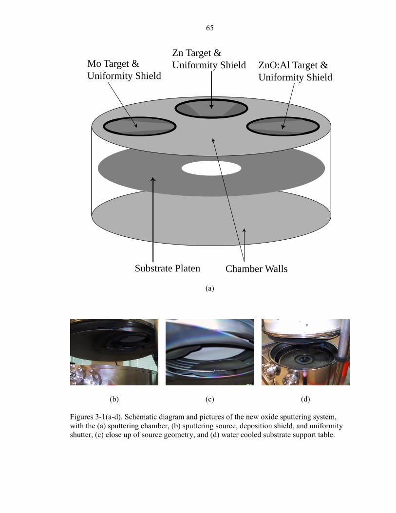
65
Mo Target &Uniformity Shield
Zn Target &Uniformity Shield ZnO:Al Target &
Uniformity Shield
Substrate Platen Chamber Walls
(a)
(b) (c) (d)
Figures 3-1(a-d). Schematic diagram and pictures of the new oxide sputtering system,with the (a) sputtering chamber, (b) sputtering source, deposition shield, and uniformityshutter, (c) close up of source geometry, and (d) water cooled substrate support table.

66
accurately positioning substrates below the sources are the primary uses for the motion
system. The throw or substrate to target distance is set at 9 cm.
A stainless steal, load-locked vacuum system is used to generate the vacuum
required for sputter deposition. A CTI 8 cryopump and a Leybold Trivac 60cfm rotary
vane pump provide the high vacuum and rough pumping, respectively. A throttle valve
between the cryopump and the deposition chamber reduces the pump’s effective pumping
speed by up to a factor of 50 when engaged. Two mass flow controllers (MFCs) are used
to regulate introduction of Ar and O2 gas, and are used in conjunction with the throttling
valve to generate a controlled gas ambient over the pressure range of 2-150 mTorr, a
range typical for sputter deposition. Both MFCs have a range of 0-100 standard cubic
centimeters per minute (SCCM), and control gases from ultrahigh purity gas bottles. The
system operates at a typical base pressure of 1.5x10⁻⁷ Torr. Vacuum gauging is provided
by an array of two Bayard-Alpert ionization gauges, two Convectron gauges, three
thermocouple gauges, and one MKS Baratron capacitance manometer. The Bayard-
Alpert gauges are used for measurements at high vacuum conditions (<10-5 Torr), and are
therefore used to determine the base pressure of the system. The base pressure is a
critical factor in controlling contamination in the growing film. The other critical gauge
is the MKS Baratron gauge, which gives accurate, precise, fast, and direct measurement
of the pressure for the range of 10-5 to 1 Torr, and therefore spans the pressure range used
for sputter deposition. A direct gauge refers to the fact that the gauge is sensitive directly
to gas pressure, and its calibration is therefore independent of the gas being measured.
This is critical for generating ambients with controlled partial pressures of a multiple gas
species.

67
3.2.2 Description of the Sputtering System
Thin films for several early experiments were deposited in a home built sputtering
system, which is affectionately known as Rusty. An illustration of the system’s bell jar
and geometry of the sources and substrate holder are shown in Figure 3-2. This system
has two RF and two DC planar magnetron sources configured in a sputter up geometry.
Each source is manufactured by US Guns Inc, is designed for a 5 cm target diameter, and
has a separate power supply. The RF supplies include a RF Plasma Products model RF-5
generator with an automatic impedance matching network, and a Plasma-Therm
generator with a manual matching network. These sources are referred to as RF1 and
RF2, respectively. The DC power supplies are a US MDX-1k and US DC-1000, and are
referred to as DC1 and DC2, respectively. The sources have power ratings of 600, 500,
1000, and 1000 watts, respectively. The substrate support has integrated temperature
control utilizing resistive Watlow cartridge heating elements, a K-type thermocouple, and
control provided by an Omega 7700 Mircomega auto-tune PID temperature controller.
The temperature control system is used to maintain accurate elevated temperatures for the
substrate during deposition.
The vacuum necessary for sputtering is generated inside a Pyrex bell jar and base
plate style chamber. A Varian 6 diffusion pump and Sargent-Welch model 1397 rotary
vane pump provide the high vacuum and rough pumping, respectively. A liquid nitrogen
cooled cryo-trap and a throttle valve are between the system and the diffusion pump.
This system has two MFCs for Ar and O2, which are used to introduce UHP gas into the
system. Vacuum gauging consists of one Bayard-Alpert ionization gauge, two
thermocouple gauges, and one MKS Baratron gauge.

68
SubstrateSupport
BellJar
BasePlate
SputterDepositionSources
SubstrateHeater
Plasma
Subtrate
Figure 3-2. Cross-sectional view of the sputter deposition system known as “Rusty”.
3.2.3 Substrate Cleaning
Soda-lime float glass was used as the substrate for the deposited films. The glass
substrates were purchase from US Precision glass, and were 5 x 5 cm square pieces seam-
ripped from larger sheets. The glass was very dirty, therefore a cleaning procedure which
involved a physical scrubbing was developed. The first step of the procedure was to
clean a 2L beaker and pyrex casserole dish with Alkonox detergent and deionized water
(DI). Then roughly 2L of water and ~30 grams of Alkonox were heated in the beaker
with a hot plate until steaming. When warm, roughly half the detergent solution was
poured into the pyrex dish, and two folded polypropylene clean room wipes were placed
on the bottom of the dish. The substrates were scrubbed on the wipes in a manner similar
to polishing a specimen. The substrates were rinsed in a spray of DI water, followed by a
scrub on both sides plus the edges with a clean brush. The substrates were rinsed again in
69
a spray of DI water, and placed in a Fluoroware wet process holder in the first tank of a
cascade rinser from Bold Technologies. When the holder was full (12 substrates), it was
run through the whole cascade rinser with N2 bubble agitation. When the substrates were
thoroughly rinsed, they were blown dry individually with a filtered dry N2 gun and place
is a storage box.
The substrates were stored in a box from Fluoroware designed to hold
photographic plates of the same size. Previous to use, the substrates were cut to the
appropriate size for the experiment (typically 2.5 x 5 cm), and then clean again by a
strong nitrogen blow.
3.3 Electrical Characterization
3.3.1 Hall Measurements
Hall measurements were used to characterize the resistivity (ρ with units of
Ω⋅cm), carrier type, carrier concentration (n with units of cm-3), and mobility (µ with
units of cm2/V⋅s). The measurements were taken by the van der Pauw method [121],
with ohmic contacts provided by electron beam deposited Al contacts patterned using a
shadow mask in intimate contact with the sample. The maximum sample size was 7 x 7
mm, with samples being cut from larger samples by a scribe and fracture procedure. The
contacts formed a 4 x 4 mm square, and each dot was approximately 0.5 mm in diameter.
The samples were mounted in a custom made shadow mask holder, placed in the electron
beam evaporation system, and the stainless steal bell jar was pumped down to ~5x10⁻⁷
Torr using a cryo-trapped diffusion pump backed by a rotary vane pump. The charge of
Al in the pocket of the Telemark electron beam deposition source was evaporated at a
rate of ~15 Å/s to generate a film thickness of ~3300 Å as measured on a Quartz Crystal

70
microbalance. A vacuum cowling covers the Hall measurement probe head to prevent
condensation during low temperature measurements, therefore Hall measurements were
performed in the dark.
The Hall system was assembled from off the shelf components. A Fieldial Field
Regulated Magnet Power Supply model V-FR2503 supplied current to a Varian
Associates large field electromagnet, which was set to an 8,000 gauss field strength. A
Keithley model 220 supplied a constant current, with a Keitley model 197 Microvolt
Digital Multimeter (DMM) used to measure the resulting voltages. A HP model 3488A
switching network connected the appropriate sample contacts to the appropriate electrical
components for the various probing geometries specified by the van der Pauw method. A
Tektronix model 177 curve tracer was integrated into the system to determine if the
contacts were ohmic by looking for the characteristic linear I-V curve. A PC controlled
all the components, and acquired and processed the data. The data reported by the
system included carrier concentration (n), mobility (µ), resistivity (ρ), carrier type, Hall
coefficient (RH), and error analysis. In operation, the system first determines the
appropriate current for the measurement. The system was programmed to supply the
current need to generate a voltage of 5 mV. For this measurement, the current was
passed through the contacts on one side of the square, and the voltage drop was measured
across the contacts on the opposite side of the square.
It is important to understand the quality of information reported by Hall
measurements, and the underlying assumptions and pitfalls associated with it. For the
case of degenerately doped ZnO:Al there are several issues which should be identified,
and some limits that need to be articulated. First is the Hall factor (γH), which is

71
generally assumed to be 1. This is a fair approximation for many semiconductors, but for
the highest possible accuracy, the value should be determined. The fact that the material
is degenerately doped can generate impurity bands, and affect the electron distribution
function (f(e)). The magnitude of the Hall voltage is another difficult issue. For samples
with low Hall mobility, the difference between the Hall voltage with and without a
magnetic field will be small, making accurate measurement of the field derived Hall
voltage difficult. This required that care be taken in analyzing the data to make sure the
changes measured due to the Hall voltage were appropriate and consistent for the
magnetic field polarity and contact geometry. These measurements are primarily used to
compare samples relative to each other. Because the same parameters are used for the
Hall system, and the films are consistently the same material, comparisons of data
between samples has the needed accuracy. Comparison with literature values for other
research in ZnO should also be reasonable since the materials parameters should be
similar. Parameters used in Hall measurements are often not reported, therefore while
comparisons with the literature are useful, they must be examined with a critical eye.
3.3.2 Four Point Probe
The measurements were taken on an Alessi four point probe. A probe head with
tungsten carbide tips with a point radius of 0.002", a probe spacing of 0.05", and a probe
pressure of 70 to 180 grams was used for all measurements. Current was supplied by a
Crytronics model 120 current source with a range of applied currents between 1µA to
100 mA. Voltages were measured by a Keithley model 181 nanovolt electrometer with
an input impedance of greater than 1 giga-ohm. Equation 3.1 and 3.2 were used to
determine sheet resistance (Rs in units of Ω/sq.) and resistivity (ρ in units of Ω·cm),
respectively.

72
RV
IS = ⋅4 532.(3.1)
ρ = ⋅ ⋅4.532 V tI
(3.2)
Based on the dimensions of the sample and probe head, no geometrical correction factors
were applied. The term t is film thickness (cm), and V is the voltage measured at the
supplied current (I).
3.4 Structural Characterization
3.4.1 Profilometry
To measure thickness of the deposited films, a portion of the substrate was
masked with a permanent marker. After the deposition, the mark was removed with
acetone and a swab, which effectively removed the deposited film on top, yielding a well
defined trench step. A Tencor Alphastep stylus profilometer was used to measure the
depth of the trench, and therefore the film thickness.
3.4.2 X-Ray Diffraction
X-ray diffraction spectra were collected on a Philips APD 3720 powder
diffractometer using Cu Kα radiation (λ=1.54056 Å). The standard settings for the X-ray
generator were 40 kV at 20 mA. Three types of θ/2θ spectra were collected for this
research, and will be designated as survey, high resolution, and line profile. Conditions
for a survey scan were a continuous scan, a 2θ range of 10° to 80°, a stepsize of 0.020°,
and a step time of 0.5 seconds. High resolution spectra were continuous scans with a 2θ
range of 30° to 40°, a step size of 0.010°, and a step time of 1.0 seconds. Line Profile
Analysis was performed on data collected with a step scan over a 2θ range of 32° to 38°,
a step size of 0.010°, and a step time of 2.5 seconds.

73
Quantification of peak full width at half maximum (FWHM) was performed using
the Philips Line Profile Analysis [122] software package. The “Approximate Analysis”
function is used, which fits a single peak with a Voight function. Broadening of the
peaks FWHM is attributed to strain and crystallite size, but the relative contribution of
each cannot be explicitly determined. Therefore only the FWHM is taken from this
technique. The software package MacDiff was used to quantify peak intensity, FWHM,
area, and 2θ peak position. For all measurements, the background was subtracted before
quantification was performed.
3.4.3 Atomic Force Microscopy
Atomic Force Microscopy (AFM) micrographs were taken with a Digital
Instruments NanoScope III. Samples roughly 7 x 7 mm were attached to a steal sample
mount with double stick tape, and placed on the magnetic holder in the instrument. The
small scanner (Scanner E) with a range of 12.5 µm in the x-y directions, and 2.5 µm in
the z direction was used to acquire all the images. The micrographs were taken in the
tapping mode with Si3N4 tips manufactured by Digital Instruments. Often more than one
image was taken from neighboring areas to make certain the images were representative
of the local area. Height and tip amplitude data were taken for each micrograph. All the
images and data were taken from height information. The amplitude information was
used to identify trouble spots due to the high sensitivity of this data to interactions
between the tip and the sample. The contrast in the amplitude image is based on changes
in the amplitude of the vibrating cantilever tip. This often gives stronger contrast than
height imaging when tip interacts differently with the surface (greater or lesser interaction
forces).

74
An automatic “Plane Fit” in the x and y directions and a “Flatten” command were
applied to the images before any analysis was performed. For the plane fit command, a
third order plane fit was used. In this procedure, the computer used a least squares
algorithm to calculate a third order polynomial for the x or y plane data, and then
subtracts this from the image data. This function serves to not only level the image, but
to reduce bowing and curvature that results from drift during data collection. The flatten
command performs a similar procedure, but applies it to each scan line. A first order
polynomial is calculated by a least squares technique, and was subtracted from each line.
This command served to line up adjacent scan lines, and reduces slope associated with
measurement drift along a scan line.
Typical data taken from AFM height images includes root mean square surface
roughness (RMS roughness), surface area difference (%), and grain size. The RMS
roughness will simply be referred to as roughness, and was measured by an algorithm in
the Digital Instruments software. The surface area difference is also quantified by the
software, and describes additional surface area of the sample relative to a flat plane with
the same x and y dimensions as the image. The grain size is determined by measuring the
grain boundary intercepts, a standard stereological technique [123]. For the data
presented, a series of eight lines 400 nm in length, and at random orientation are laid on
the image. The topography of the line is displayed in cross section. Intercepts are
determined by using low points on the cross section plot, and careful observation and
comparison with full image. This is done for each of the eight lines, and an average is
calculated. The grain size is determined by dividing the length of the line by the average
number of intercepts. This stereological technique is based on the assumption that the

75
sample has equiaxed grains typical of bulk samples for which this technique was
developed. In addition to the caveat in the previous statement, the number of intercepts is
based on interpretation of low features between hillocks as grain boundaries, therefore
the grain size must be used carefully for analyses.
3.4.4 Auger Electron Spectroscopy
Auger electron spectroscopy (AES) measurements were taken on a PHI model
660 Scanning Auger Microprobe (SAM). This system utilizes a LaB6 thermonic
emission electron source with a co-axial Cylindrical Mirror Analyzer (CMA) to measure
the kinetic energy of Auger electrons, these energies being characteristic of the elements
generating them. A thorough description of the Auger analysis is beyond the scope of
this work, but is covered in depth in several books [124,125]. AES is considered a
surface analysis technique because the detected Auger electrons can only escape from
within the first several monolayers below the sample surface. The CMA is sensitive to
distance between itself and the sample, and is therefore calibrated using the standard
elastic peak technique. The system has an Ar ion beam source, which is used to sputter
etch the sample’s surface. It was used to clean contaminants from the surface, remove
surface layers to get compositional information more representative of the film’s “bulk”,
and to perform depth profiles. The parameters used for the ion beam source are an
accelerating potential of 3 kV, a beam current of ~90 nA, and a spot area of
approximately 1 mm2. The rate and area of the etch are influenced by the rastering
conditions applied to the beam, with a 3 x 3 mm raster pattern at the specimen being the
standard setting. The system was maintained at a base pressure on the order of 10-10 Torr,
and typically operated at 10-8 Torr while the Ar ion source was in use.

76
The two types of AES data presented in the work are survey spectra and depth
profiles as a function of sputter etching time. For all spectra, a primary beam energy of 5
kV was used. Ten replicates of the spectrum of counted electrons at an energy (n(E))
versus kinetic energy (KE) are summed over the energy range of 50 to 2050 eV. This
data is taken with an energy step size of 1.0 eV, and a dwell time of 30ms at each energy.
This spectrum is then numerically differentiated by an algorithm from the computer
acquisition system’s software to yield the spectrum in terms of d(n(E))/d(E) versus KE.
The differentiated spectrum is then used to accurately determine kinetic energy of the
Auger electron peaks, which in turn is used to determine the elements present on the
sample’s surface. The differentiation algorithm also has a smoothing function, which can
operate across a user determined cell size. It was left at the standard setting of 9 for all
data presented in this dissertation. To account for charge shifting, peak energies were
referenced to adventitious carbon (272 eV) if possible.
Depth profile data was taken using the window method, which involves
alternating between sputter etching the sample and collecting small windows of Auger
spectra focused on the peaks for elements of interest. This signal from each Auger
window is then differentiated, using the same algorithm as the survey spectra. The peak-
to-peak heights of the differentiated spectra are plotted as a function of element and
sputter etching time. Parameters used for collecting depth profiles are presented in Table
3-1.
3.4.5 X-ray Photoelectron Spectroscopy
X-ray photoelectron spectroscopy (XPS) is also known as Electron spectroscopy
for chemical analysis (ESCA). XPS spectra were taken on a PHI model 5100 ESCA
system. A non-monochromated Mg Kα X-ray source, producing characteristic radiation

77
Table 3-1. Parameters used for Auger electron sepectroscopy sputter depth profiles.Element Oxygen Zinc SiliconPeak Energy (eV) 506.0 984.5 1601.0Window Boundary – Low (eV) 475.0 946.0 1585.0Window Boundary – High (eV) 525.0 1025.0 1615.0Dwell Time (ms) 50 50 50Number of Sweeps 10 10 10
with a peak photon energy at 1253.6 eV was used for all spectra. The X-ray generator
was operated at 15 kV and 300 watts (20 mA). Photoelectrons liberated from the sample
are collected, retarded, and analyzed in a hemispherical analyzer. The analyzer acts as a
band pass filter, allowing only electrons with a particular kinetic energy through to the
Channeltron detector. The kinetic energy is converted into binding energy through use of
Equation 3.3:
BE h - KE - D= ν φ (3.3)
where BE is the binding energy of the detected electron, h is Planck’s constant, ν is the
frequency of X-ray probe beam, KE is the kinetic energy of the photoelectron, and φD
(4.7 eV) is the work function of the detector (hemispherical analyzer). Spectra are
traditionally presented starting with the highest binding energy to the lowest on the
abscissa.
The based pressure of the system is on the order of 10-10 Torr, and typically
operates at 10-8 Torr if the Ar ion gun is being used for sputter etching. Similar to AES,
XPS is also a surface analysis techniques due to the limited escape depth of measured
photoelectrons. Argon ion etching was used to remove surface contaminants and to erode
into the thin films to gather information from a region that can reasonably be considered
the “bulk” of the thin film. The conditions used for the ion source were an accelerating
potential of 4 kV and a beam raster area of 4 x 7 mm at the specimen’s surface.

78
The two types of XPS data taken include survey spectra and multiplex spectra.
Survey spectra had binding energies from 1100 to 0 eV, and were taken with an energy
resolution of 0.5 eV per step, a dwell time of 30ms, a pass energy of 89.45 eV, and a take
off angle of 45°. The measured peaks were correlated to tabulated energies and spectra
for the elements to determine the elements present at the sample surface.
Multiplex scans take data across a series of small energy ranges (windows) in
order to gather more accurate data on peaks of interest found in survey scans. Parameters
used to collect the multiplex scans are presented in Table 3-2. Qualitative atomic
concentrations of elements on the surface were determined from the area of the elemental
peaks in conjunction with sensitivity factors. The multiplex data were also used during
peak deconvolution. The deconvolution process involves choosing a peak from a
Multiplex window, subtracting the background and fitting the peak with one or more
component Gaussian-Lorentzian functions. The variables for these functions included
peak energy, height, full width at half maximum (FWHM), and percentage Gaussian. All
peaks were fitted by a combination of manual and automatic fitting. This technique was
used to accurately determine the character of the peak for investigating of the chemical
bonding.
Table 3-2. Parameters used to collect XPS multiplex scans.Element Oxygen Carbon ZincWindow Boundary – High (eV) 536.0 292.0 1032.0Window Width (eV) 10.0 15.0 20.0eV/Step 0.1 0.1 0.1Time/Step (ms) 50 50 50Pass Energy (eV) 35.75 35.75 35.75Sweeps 10 10 10

79
3.4.6 Secondary Ion Mass Spectrometry
Secondary Ion Mass Spectrometry (SIMS) was used to measure the composition
of the deposited films, with particular interest in concentrations of electrically active
dopants and contaminants. The SIMS spectra were collected on a Perkin-Elmer PHI
6600. Data were acquired using an oxygen primary ion beam from a duoplasmatron
source and positive secondary ion acquisition. The primary beam energy was 6 keV with
a beam current of 209 nA. The primary beam was rastered over either a 400 x 400 µm or
500 x 500 µm area, and used a gating of 65%. A quadrupole mass filter was used to pass
secondary ions with a specific charge to mass ratio to the secondary ion detector. The
detected signal was intensity, or counts per second, for the secondary ions as a function
of the charge to mass ratio being passed by the mass filter. The systems neutralizer was
utilized to avoid sample charging during collection of the spectra.
The two types of SIMS data collected include survey spectra from the as
deposited surface, and depth profiles. Survey spectra were used to determine the
elements present on the surface, with secondary ion intensity plotted versus the mass to
charge ratios over the range 1 to 110. Depth profiles measure the signal from the mass to
charge ratio for elements of interest as a function of sputtering time. This is used to
characterize changes in composition through the thickness of the film. Elements of
interest that were profiled include C(12), Na(23), Mg(25), Al(27), Si(28), Ca(40), Al(54)
and Zn(66). The number in parenthesis specifies the particular isotope followed during
the depth profile, with the exception for Al(54), which is the dimer of Al(27).

80
3.5 Optical Properties
3.5.1 Spectrophotometry
Optical spectrophotometry measurements were taken on a Perkin-Elmer Lambda
9 system from the UV region into the Near IR region in order to obtain spectral features
associated with the band edge and plasma resonance phenomena. Transmission spectra
were collected at normal incidence, using a double beam geometry with a sampling and a
reference beam. For all measurements, the reference path was left open. The glass
background spectrum was removed by collecting and averaging a series of 4 spectra from
bare glass, and dividing measurements taken from the sample by the averaged glass
spectrum. The optical beam size on the sample was roughly 3 x 0.3 cm. The diffraction
grating is changed at 860 nm, and yields a small discontinuity in the collected spectra. A
tungsten lamp source provides the light for the measurements.
3.5.2 Fourier Transform Infrared Spectroscopy
Fourier transform infrared (FT-IR) spectra were collected using a Nicolet model
510p spectrophotometer in reflection mode. The measurements where made using a
variable angle reflectance stage, and measurements where typcially taken at 30° and 60°.
Data were collected at two angles to gauge the influence of measurements above and
below the Brewster angle [126], and to have two spectra for more accurate comparison to
spectra generated by a model. Calibration to remove the background was performed
using a gold mirror standard. Measurements were then made on both sides of the
substrate (glass and film) at both angles of incidence. These spectra were compared to
spectra generated by a model developed by George Alameddin. Film thickness, carrier
concentration, infrared damping coefficient, and optical constants for the film and
substrate were the parameters entered into the model. By changing the parameters, the

81
calculated spectra were matched to the measured ones. Thus, values for the modeled
parameters could be determined from the FT-IR spectra. The infrared damping
coefficient is inversely related to mobility, thus carrier concentration and mobility can be
estimated.
3.6 Experimental Procedures
3.6.1 Affect of Annealing Ambient on the Properties of ZnO:Al
The objective of this experiment was to determine the sensitivity of ZnO:Al thin
films to modest heat treatments, and to determine if the gas ambient in the furnace had a
strong influence on the results of the heat treatment. The films for this experiment were
deposited in Rusty with cleaned 2.5 x 5 cm pieces of glass used as substrates. The
parameters held constant for deposition of the thin films are as follows:
• Target: ZnO:Al2O3 (98wt%:2wt%) hot pressed
• Base Pressure: 8x10⁻⁷ Torr
• Substrate to Target distance: 4 cm
• Process Pressure: 5 mTorr Ar (UHP)
• Ar Flow Rate: 7 sccm
• RF Power: 100 watts forward, <2 watts reflected
• Substrate Temperature: Unheated
The as deposited samples were characterized by stylus profilometry,
spectrophotometry, FT-IR, XRD, and four point probe measurements. Profilometry
measurements were made by the standard procedures previously outlined.
Spectrophotometry measurements were taken on a Perkin-Elmer Lambda 9 over the
range of 300 to 2000 nm using the previously outlined standard procedures. FT-IR

82
measurements were taken in reflection mode, with a 60° incident angle from the surface
normal using standard procedures. XRD diffraction measurements were taken by loading
the sample directly into the diffractometers chuck, resulting in data taken roughly from
the center of the sample. Both survey and high resolution spectra were collected, and
each high resolution measurement was repeated after removing and remounting the
sample in the diffractometer. The replicate data were used to judge the repeatability of
the measurements. Four point probe data were taken from three different positions, one
near each end, and one from the middle, and is illustrated in Figure 3-3.
Four of the samples heat treated in a quartz tube furnace with ambients of N2,
forming gas (N2/H2 90%:10%), stagnant air, and O2. The fifth sample was used as a
control, and was therefore not heat treated. To heat treat the samples, the furnaces were
warmed up to 400°C and purged with the appropriate gas for at least one hour, with the
sample in the furnace, but out of the hot zone. The samples were then pushed with a
small push rod into the hot zone of the furnace, and remained there for 1hr and
15minutes. The samples where then pulled out with the push rod, cooled in the area
12 3
Figure 3-3. Positions on the 2.5 x 5 cm substrate where four point probe data werecollected.

83
outside the hot zone but still within the controlled ambient of the furnace. When cooled
to approximately 75°C, the samples were removed from the furnace and rapidly
quenched to room temperature. The samples were then recharacterized by the same
procedures used before the heat treatment.
3.6.2 Development of Properties in Very Thin ZnO:Al Films
The objective of this experiment was to investigate the development of structural
and electrical properties of ZnO:Al thin films, and relate those characteristics to thickness
dependent effects in the electrical properties. The thin films were deposited in Rusty
onto cleaned 2.5 x 2.5 cm glass substrates. Standard permanent marker stripes were
made before each run for profilometry measurements. Also, the substrate’s surface was
cleaned with a strong N2 blow just prior to introduction into the deposition system. The
deposition parameters held constant are as follows:
• Target: ZnO:Al2O3 (98wt%:2wt%) hot pressed
• Base Pressure: 8x10⁻⁷ Torr
• Substrate to Target distance: 5 cm
• Process Pressure: 5 mTorr Ar (UHP)
• Ar Flow Rate: 7 sccm
• RF Power: 100 watts forward, <2 watts reflected
• Substrate Temperature: 150°C
• Substrate Geometry: Substrates were positioned off axis (not directly above the source)
The parameter varied during this experiment was the deposition time, which was
used to control film thickness. Deposition times of 10, 20, 30, 60, 180, 300, 420, and 900
seconds were used. The deposition rate at the conditions used was measured by

84
profilometry to be 1.75 Å/s. The thickness was determined by multiplying the deposition
rate by the deposition time. Additionally, the films were characterized by four point
probe, Hall measurements, AFM, and AES. Four point probe and Hall measurements
were used to characterize ρ, n, and µ. The 7 x 7 mm samples for Hall Measurements
were cleaved from the substrates edge closest to the deposition source. Four point probe
measurements were taken from the edge closest to the source, middle of the substrate,
and the edge farthest from the source.
Analysis of AFM micrographs was used to determine the surface morphology of
the thin films. The technique of AES was used to look for contaminants, and to
investigate surface coverage of the sample. Two survey spectra where collected using the
standard parameters, with a sample tilt of 45° and a sample beam current of ~50 nA, one
before and one after a depth profile. The profile was collected using window scans, using
the parameters specified previously. The Auger data from the window scans were
differentiated, and peak-to-peak heights were used to evaluate changes in the surface
composition. To determine the surface fraction covered by the film, atomic
concentrations were taken from an as deposited survey spectrum using the standard
procedures in the instrument’s software. These were compared to atomic concentration
measured for a pure ZnO:Al and pure glass surfaces. The atomic concentrations
measured on the as deposited surface were evaluated relative to the pure surface
standards, and from this a fractional surface coverage for the film was estimated.
3.6.3 Negative Ion Resputtering in Sputter Deposition of ZnO:Al Films
The objective of this experiment was to determine the role of negative ion
resputtering (NIR) during sputter deposition of ZnO:Al thin film, and the influence of RF
power on the magnitude of the NIR effect. The films for this experiment were deposited

85
in NOSS. All thin films were deposited onto soda-lime glass substrates cleaned by the
procedures given above.
The substrate consisted of 2.5 x 5 cm pieces of glass, with three pieces of glass
placed end to end to effectively make one 2.5 x 15 cm substrate. One end of the substrate
was placed under the center of the sputter deposition source, and was arranged
perpendicularly to the edge of the uniformity shield to minimize film thickness gradients
across the 2.5 cm dimension of the substrate. A side view of the system was presented in
Figure 2-22, and schematically showed the generation and acceleration of negative ions
away from the deposition source. The top view illustrates the position of the substrate
relative to the deposition source and is presented in Figure 3-4.
The sample deposited at 500 watts is an important exception to this substrate
geometry. For this sample, instead of the end of the substrate coming to the center of the
Substrate
Top View
ZnO:Al Targetz
Uniformity Shields
Figure 3-4. Top-view of the deposition geometry used for the investigation of negativeion resputtering, with the substrate extending from the center to the edge of the source.

86
source, it was translated away in the radial direction (the direction along the long axis of
the substrate) approximately 3.2 cm based on trends in the data. Before the substrates
were placed in the system, a stripe was made down the long axis of the substrate near the
edge with a fine point permanent marker for standard profilometry measurements.
The order of the depositions was 500 watts, 250 watts, and 1000 watts. The 500
watt sample was deposited by itself, while the 250 and 1000 watt samples were both
loaded on opposite ends of the substrate platen and done as a single run. After the 250
watt sample was deposited, the stepper motor was used to rotate the platen such that the
substrate for the 1000 watt deposition was in position. The deposition shutter was closed
during substrate rotation and retuning of the source for 1000 watts. The conditions held
constant for the depositions are as follows:
• Base Pressure: 1.5x10⁻⁷ Torr
• Substrate to Target distance: 9 cm
• Process Pressure: 5 mTorr Ar (UHP)
• Ar Flow Rate: 3.2 sccm
• Presputtering: 10 minute at 250 W with deposition shutter closed
• Substrate temperature: room temperature (by chilled water)
The power, deposition time, and position on the substrate were treated as
variables. The position on the substrate was measured along the edge near the
profilometry mark, with the end of the substrate under the source as the origin. A list of
the varied deposition parameters follows. The deposition time was changed in order to
keep the thickness of the deposited films within the same order between conditions,

87
thereby minimizing the influence of variable thickness between the different deposition
conditions.
• 250 watts for 60 minutes
• 500 watts for 60 minutes
• 1000 watts for 20 minutes
After deposition, a series of small marks were scribed on the samples every 0.6
cm near the stripe used for profilometry measurements. Using the optical camera in the
profilometer, these marks could be found, allowing thickness measurements to be made
at precise locations. The marks were also used for positioning four point probe
measurements, which were taken with the geometry of the four points arrayed
orthogonally to the long axis of the substrate. Since the film thickness is the same across
the short axis of the substrate, the thickness data can be used in Equation 3.2 to calculate
film resistivity accurately as a function of position along the long axis of the substrate.
In order to get XRD data from particular positions, the substrate was cleaved into
three equal sections (2.5 x 1.7 cm) perpendicular to the long axis. These samples were
mounted to microscope slides with double-sided tape. In order to assure the film surface
was positioned correctly, a dummy piece of glass of the same type used for a substrate
was also attached to the microscope slide, such that it was in the sample chuck and the
film was on the sampling plane. For this experiment, both survey and line profile spectra
were collected.
Hall and AFM measurements require samples significantly smaller than those
used for the XRD measurements, therefore each XRD sample was further subdivided to
yield two roughly 7 x 7 mm samples. The sample for Hall measurements had Al dot

88
contacts deposited as previously described, and measurements were made using the
standard procedures. After Hall measurements, SIMS was used to characterize the
composition of the Hall samples using the previously described conditions. An oxygen
primary beam was used for positive SIMS, because the concentration of electropositive
elements is the focus of this characterization. In particular, the ratio of Zn to Al, and Zn
to the alkali metals were pursued because they dope and compensate ZnO, respectively.
The AFM sample was then characterized. The information used for this experiment
included grain size, RMS roughness, surface area difference, and surface morphology.
X-ray photoelectron spectroscopy was used to characterize the composition and
chemical bonding for the surface of the deposited film. Standard survey scans using the
previously mentioned conditions were first collected. Multiplex scans were then
performed for O, C, and Zn using the conditions specified above. Sputter etching of the
film using the ion source at standard conditions for six minutes was performed to remove
surface contaminants from the ambient, and was followed by survey and multiplex scans
using the same conditions as those used prior to sputter etching.

89
CHAPTER 4AFFECT OF ANNEALING AMBIENT
4.1 Background
The resistivity of ZnO:Al films deposited in early experiments were typically very
high (ρ>10-2 Ω·cm), and varied by orders of magnitude with small changes in position on
the sample’s surface. Best results were achieved for small areas of some films with
values on the order of 10-3 to 10-2 Ω·cm. Numerous reports in the literature
[11,91,92,127] indicate that modest heat treatments in reducing ambients could yield
large decreases in resistivity for ZnO:Al thin films. Reported heat treatments were
typically performed at temperatures between 300 and 400°C, for durations of between
half an hour and several hours and in reducing gas ambients based on combinations of
hydrogen and inert gas. Heat treatments at these temperatures are not compatible with
the thermal budget imposed for ZnO:Al films as part of a solar cell structure. Thus, while
not practical in the context of fabricating a device, characterization of effects resulting
from heat treatments provides data regarding potential of deposited films to achieve
better properties, and helps define the cause of high resistivity.
Preliminary experiments indicate that annealing in a high purity forming gas
ambient can significantly reduce resistivity of deposited films. From this experiment,
annealing conditions of 400°C for one hour is chosen, with flowing gas for all gas
ambients except stagnant air. The control sample is not annealed and instead was used to
assess aging effects and experimental error. Goals of the experiment were to learn the
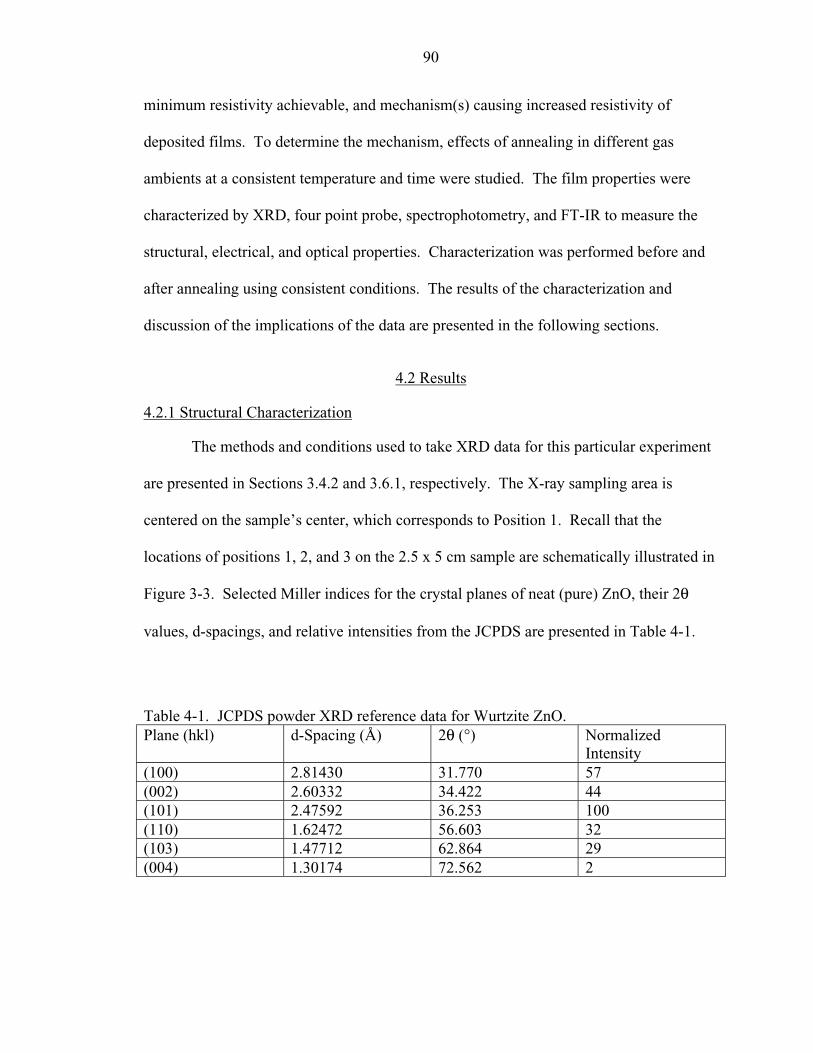
90
minimum resistivity achievable, and mechanism(s) causing increased resistivity of
deposited films. To determine the mechanism, effects of annealing in different gas
ambients at a consistent temperature and time were studied. The film properties were
characterized by XRD, four point probe, spectrophotometry, and FT-IR to measure the
structural, electrical, and optical properties. Characterization was performed before and
after annealing using consistent conditions. The results of the characterization and
discussion of the implications of the data are presented in the following sections.
4.2 Results
4.2.1 Structural Characterization
The methods and conditions used to take XRD data for this particular experiment
are presented in Sections 3.4.2 and 3.6.1, respectively. The X-ray sampling area is
centered on the sample’s center, which corresponds to Position 1. Recall that the
locations of positions 1, 2, and 3 on the 2.5 x 5 cm sample are schematically illustrated in
Figure 3-3. Selected Miller indices for the crystal planes of neat (pure) ZnO, their 2θ
values, d-spacings, and relative intensities from the JCPDS are presented in Table 4-1.
Table 4-1. JCPDS powder XRD reference data for Wurtzite ZnO.Plane (hkl) d-Spacing (Å) 2θ (°) Normalized
Intensity(100) 2.81430 31.770 57(002) 2.60332 34.422 44(101) 2.47592 36.253 100(110) 1.62472 56.603 32(103) 1.47712 62.864 29(004) 1.30174 72.562 2

91
The XRD spectra are presented in Figures 4-1(a-b) to 4-5(a-b), with survey
spectra (10°<2θ<90°) shown in (a) and high resolution spectra (30°<2θ<40°) shown in
(b). The labeled red dashed vertical lines on all XRD spectra mark the JCPDS listed 2θ
positions for peak from Table 4-1. The plot for each gas ambient shows the results from
before and after the heat treatment in the specified gas ambient. For high resolution data,
two traces are plotted for data taken before heat treatment (blue and pink) for each gas
ambient used, which are replicate spectra. The excellent overlap of replicate data
indicates measurement precision is high.
Survey spectra show three dominant peaks corresponding to (100), (002), and
(110) ZnO crystal planes. A weak but recognizable peak for the (101) plane can be
appreciated in data from annealed samples. Diffraction peaks from several JCPDS listed
crystal planes are missing, and intensities from detected peaks do not match the listed
normalized intensities. Also, run-to-run variations in peak intensities for the three
dominant peaks, as well as variations in the relative intensities between the three peaks
for a particular sample occur in the spectra. The presence of changes with heat treatment
in peak position, intensity, and FWHM can be appreciated in high resolution and survey
spectra for all gas ambients. Intensities increase and breadths decrease for all peaks with
heat treatment, while both increases and decreases occur in 2θ peak positions. To
investigate these variations, peak position (degrees), intensity (counts), peak area, and
full width at half maximum (FWHM in degrees) data are quantified from (100) and (002)
peaks from before and after annealed conditions using the MacDiff [128] software
package. Data are not quantified from the (110) peak, which is the third dominant peak,
because this peak does not fall within the 2θ range for high resolution data. Data are

92
0
200
400
600
800
1000
1200
1400
1600
1800
10 20 30 40 50 60 70 80 90
2θ (°)
Cou
nts
(100
)(0
02)
(101
)
(110
)
(103
)
(004
)
Before Anneal After Anneal
(a)
0
2000
4000
6000
8000
10000
12000
30 32 34 36 38 402θ (°)
Cou
nts
Before AnnealBefore AnnealAfter Anneal
(100
)
(002
)
(101
)
(b)
Figures 4-1(a-b) X-ray diffraction spectra from before and after a ZnO:Al thin film isannealed in nitrogen with (a) survey spectra and (b) high resolution spectra focusing onthe (002) peak.

93
0
200
400
600
800
1000
1200
1400
1600
1800
10 20 30 40 50 60 70 80 90
2θ (°)
Cou
nts
(100
)(0
02)
(101
)
(110
)
(103
)
(004
)
Before Anneal After Anneal
(a)
0
2000
4000
6000
8000
10000
12000
30 32 34 36 38 402θ (°)
Cou
nts
Before AnnealBefore AnnealAfter Anneal
(100
)
(002
)
(101
)
(b)
Figures 4-2(a-b) X-ray diffraction spectra from before and after a ZnO:Al thin film isannealed in forming gas with (a) survey spectra and (b) high resolution spectra focusingon the (002) peak.

94
0
200
400
600
800
1000
1200
1400
1600
1800
10 20 30 40 50 60 70 80 90
2θ (°)
Cou
nts
(100
)(0
02)
(101
)
(110
)
(103
)
(004
)
Before Anneal After Anneal
(a)
0
2000
4000
6000
8000
10000
12000
30 32 34 36 38 402θ (°)
Cou
nts
Before AnnealBefore AnnealAfter Anneal
(100
)
(002
)
(101
)
(b)
Figures 4-3(a-b) X-ray diffraction spectra from before and after a ZnO:Al thin film isannealed in stagnant air with (a) survey spectra and (b) high resolution spectra focusingon the (002) peak.

95
0
200
400
600
800
1000
1200
1400
1600
1800
10 20 30 40 50 60 70 80 90
2θ (°)
Cou
nts
(100
)(0
02)
(101
)
(110
)
(103
)
(004
)
Before Anneal After Anneal
(a)
0
2000
4000
6000
8000
10000
12000
30 32 34 36 38 402θ (°)
Cou
nts
Before AnnealBefore AnnealAfter Anneal
(100
)
(002
)
(101
)
(b)
Figures 4-4(a-b) X-ray diffraction spectra from before and after a ZnO:Al thin film isannealed in oxygen with (a) survey spectra and (b) high resolution spectra focusing onthe (002) peak.
96
0
200
400
600
800
1000
1200
1400
1600
1800
10 20 30 40 50 60 70 80 90
2θ (°)
Cou
nts
(100
)(0
02)
(101
)
(110
)
(103
)
(004
)
Before Anneal After Anneal
(a)
0
2000
4000
6000
8000
10000
12000
30 32 34 36 38 402θ (°)
Cou
nts
Before AnnealBefore AnnealAfter Anneal
(100
)
(002
)
(101
)
(b)
Figures 4-5(a-b) X-ray diffraction spectra from before and after a ZnO:Al thin film usedas a control sample (a) survey spectra and (b) high resolution spectra focusing on the(002) peak.

97
taken from peaks with the background subtracted and the peak fitted with an
approximated Voight function. Quantified data from (100) and (002) peaks from before
and after heat treatment are presented in Tables 4-2 and 4-3, respectively.
Changes of less than 5% occur in all data between before and after annealing as
compared to the control sample, indicating good measurement precision. This fact plus
the good agreement between replicate spectra taken prior to annealing indicates good
precision for both measurement and quantification of the data. For (100) data, all 2θ
peak positions were smaller than the JCPDS value of 31.770°. The 2θ peak positions
Table 4-2. Quantified XRD data from (100) diffraction peak.(100) Peak
Ambient
2θ position(°)
Before After
Intensity(Counts)
Before After
Peak Area
Before After
FWHM(°)
Before AfterNitrogen 31.20 31.41 578 1125 61427 87095 0.986 0.688
Forming Gas 31.19 31.50 850 1629 82154 113826 0.883 0.624Stagnant Air 31.22 31.47 702 1329 67061 99022 0.871 0.662
Oxygen 31.23 31.50 839 1514 76569 110177 0.827 0.644Control 31.21 31.20 837 875 82984 84470 0.901 0.875
Run-to-RunVariation
0.18% 0.28% 36% 36% 30% 26% 18% 10%
Table 4-3. Quantified XRD data from (002) diffraction peak.(002) Peak
Ambient
2θ position(°)
Before After
Intensity(Counts)
Before After
Peak Area
Before After
FWHM(°)
Before AfterNitrogen 34.30 34.29 3547 6393 427798 471969 1.038 0.632
Forming Gas 34.40 34.32 5256 9845 631750 688551 0.988 0.597Stagnant Air 34.37 34.31 3019 6273 409778 492042 1.148 0.679
Oxygen 34.30 34.32 1546 3695 231186 303162 1.357 0.713Control 34.28 34.31 1137 1134 147445 150687 1.158 1.194
Run-to-RunVariation
0.34% 0.09% 128% 90% 124% 78% 30% 18%

98
shift 0.2 to 0.3° higher with annealing for all gas ambients, bringing them closer to the
JCPDS value. The peak intensity from the (100) plane is consistently the lowest of the
three dominant peaks. Intensity relative to background increases by 80 to 95% with
annealing. The (100) peak area is consistently much less than the (002) peak. Peak area
increases between 39% and 48% with annealing, which is substantially smaller than the
increase in peak intensity. Before heat treatment, the (002) FWHM values are
consistently larger than for (100) values, while after heat treatment (002) FWHM values
are consistently smaller than for the (100) peak. For all cases, the FWHM decreases with
heat treatment at 400°C for 60 minutes. The (100) FWHM decreases by 22 to 30% with
heat treatment. Significant run-to-run variation is found from samples with and without
heat treatment in the data for intensity, peak area, and FWHM, while little variation
outside experimental error occurs for 2θ peak position. Run-to-run variation in peak
intensity and peak area is significantly higher than variation in FWHM.
For the (002) peak, the 2θ peak position is always lower than the JCPDS listed
value of 34.422°. Peak position decreases for samples annealed in forming gas and
stagnant air, but does not change outside of experimental error for nitrogen or flowing
oxygen anneals. Intensity of the (002) peak is typically highest except for the control
sample for which the (110) peak is most intense. Intensity increases by 80%, 87%,
108%, and 139% with heat treatment in nitrogen, forming gas, stagnant air, and oxygen,
respectively. Peak area also increases by 10%, 9%, 20%, and 31% with annealing in
nitrogen, forming gas, stagnant air, and oxygen, respectively. This increase is much
smaller than those measured for peak intensity. The FWHM decreases by 39%, 40%,
41%, and 47% with annealing in nitrogen, forming gas, stagnant air, and oxygen,

99
respectively. All FWHM values are significantly higher than the lowest values reported
from experiments in Chapter 6, which are approximately 0.3°. Run-to-run variations are
large and have similar values both before and after heat treatment for peak intensity and
peak area. The FWHM shows less variation, but the 30% and 18% variation that occurs
for data from before and after heat treatment are still significant. Run-to-run variation in
2θ peak position is very small, and for data taken after heat treatment, no variation
outside of experimental error occurs.
4.2.2 Electrical Characterization
Four point probe measurements are taken as discussed in the experimental
methods section (3.3.2). The current and voltage data were combined with the thickness
(~0.5 µm) to determine the film’s resistivity. Resistivity as a function of before and after
the 400°C one hour heat treatment, gas ambient, and position on the substrate appear in
Table 4-4. As shown in Figure 3-3, positions 1,2, and 3 correspond to center, left side,
and right side of the 2.5 x 5 cm sample, respectively. The term NC in Table 4-4 refers to
“no compliance”, which occurs when the current source is unable to drive the selected
current. This occurs when the sample’s resistance is too high, and typically occurs for
ZnO:Al films with resistivities > 102 Ω·cm for film thicknesses in this experiment.
Measurable resistivities vary by more than five orders of magnitude, and no
compliance results suggest higher resistivities are present. Four classes of variations are
found in the data and include positional, run-to-run, heat treatment, and heat treatment
ambient. With position, maximum variations of greater than four orders of magnitude
and three orders of magnitude occur for data taken before and after annealing,
respectively. The smallest variations with position are approximately a factor of 3 and 2

100
Table 4-4. Resistivity data from before and after heat treatment measured by four pointprobe as a function of position and gas ambient used.
Ambient Position 1(Ω·cm)Before After
Position 2 (Ω·cm)Before After
Position 3 (Ω·cm)Before After
Nitrogen 560 1.69 194 5.83 3.44x10⁻² 1.30x10⁻²
Forming Gas 0.665 4.65x10⁻³ 9.63x10⁻² 3.13x10⁻³ 1.42x10⁻² 1.71x10⁻³
Stagnant Air NC 41.8 1.01 0.256 4.74x10⁻² 4.21x10⁻²
Oxygen NC 109 4.42x10⁻² 2.35 1.66 11.3Control (No Anneal) NC NC 1.68x10⁻² 1.30x10⁻² 34.6 29.8
for before and after annealing, respectively. Also, as deposited resistivities are
consistently highest for position 1, corresponding to the sample’s center. Many
resistivities are too high to be measure prior to annealing, as shown by the NC values
which are only found at position 1. After annealing, position 1 resistivities are highest
for samples annealed in forming gas, stagnant air, and oxygen, but position 2 has the
highest resistivity for the sample annealed in nitrogen.
Run-to-run variations in resistivity occur in data from both before and after heat
treatment. Comparison of resistivities from the same position on the sample must be
used to assess run-to-run variations due to the large effect position has on resistivity.
Run-to-run variations in resistivity for annealed films are confounded by effects of
different ambients used, therefore the data will be highlighted subsequently. Prior to
annealing, resistivities range from 0.67 to >560 Ω·cm, 1.7x10⁻² to 190 Ω·cm, and
1.4x10⁻² to 35 Ω·cm for data taken from positions 1, 2, and 3, respectively. Data from as
deposited films indicates that despite care to use consistent deposition and
characterization conditions, more than three orders of magnitude in variation occurs for
resistivity data. This indicates that large variations occur for all three measurement
positions. The relatively small variation between repeated measurements from the

101
control sample of 26% and 15% for positions 2 and 3, respectively, suggest measurement
variation is not responsible for the large run-to-run differences.
The 400°C, one hour anneal typically changes the sample’s resistivity, but the
magnitude of the changes show significant variation. Annealing typically decrease the
resistivity, except for the oxygen ambient case where resistivities increase for some
positions. Differences in the response of resistivity to gas ambient used in annealing will
be presented subsequently. Because results change with gas ambient, variations in
response to the heat treatment must be investigated by looking at positional variations on
samples annealed in the same ambient. To facilitate investigation of changes in
resistivity with heat treatment, Table 4-5 presents the magnitudes of changes in resistivity
with annealing. The ? signifies the resistivity values both before and after annealing are
too high to be measured.
The largest resistance changes are found for position 1, which also had the highest
initial resistivity. Changes in resistivity for position 2 are consistently larger than
changes for position 3 despite similar initial resistivities. Focusing on resistivity changes
for particular gas ambients, annealing in nitrogen lead to the largest change with a 331
times reduction in resistivity for position 1. For position 3, a 2.6 time reduction in
resistivity occurs. The larger change occurs with a higher initial value. The lowest
resistivity of 1.30x10⁻² Ω·cm is not significantly lower than several as deposited values.
For forming gas, large decreases in resistivity occur for all positions. Also, all resulting
resistivities are significantly lower than any as deposited resistivities from this
experiment. The variation in resistivity with position is the smallest found for this
experiment. The as deposited resistivities for this sample are also among the lower as

102
Table 4-5. Changes in resistivity with 400°C one hour annealing.Ambient Position 1
∆ρPosition 2
∆ρPosition 3
∆ρNitrogen -331x -33x -2.6x
Forming Gas -143x -31x -8.3xStagnant Air >-10x -3.9x -1.1x
Oxygen >-5x +53x +6.6xControl (No Anneal) ? -1.3x -1.2x
deposited resistivities, particularly for position 1. For stagnant air, little change occurs
for position 2, and no change outside of experimental error occurs for position 3. The
initial resistivity for position 2 is higher than position 3. More than an order of
magnitude change occurs for position 1 when it is considered that the NC value is greater
than 5x10² Ω·cm, but the magnitude of the change is not known. For oxygen, at least a
factor of 5 decrease in resistivity occurs. In contrast, a factor of 53 and 7 increase in
resistivity occur for positions 2 and 3, respectively. The initial value for position 1 is
much higher than the initial values for either position 2 or 3.
4.2.3 Optical Characterization
Optical spectrophotometry in transmission and Fourier transform infrared
spectroscopy measurements in reflection are collected for this experiment. All
measurements are taken from the film’s center, corresponding to position 1.
Transmission is measured over the wavelength range of 300<λ<2000 nm and are
presented in Figure 4-6 (a-e). Each plot contains a spectrum from the bare glass
substrate, and the glass substrate coated with as deposited films, and films annealed at
400°C for one hour in flowing nitrogen, flowing forming gas, stagnant air, flowing
oxygen, and the unannealed control sample. Thin film optical interference fringes are
observed as oscillations in the transmittance for data from coated substrates. Reported

103
0
0.2
0.4
0.6
0.8
1
300 500 700 900 1100 1300 1500 1700 1900
Wavelength (nm)
Tra
nsm
issi
on (
%)
Before Anneal
After Anneal
Glass
Interference Fringes(a)
0
0.2
0.4
0.6
0.8
1
300 500 700 900 1100 1300 1500 1700 1900
Wavelength (nm)
Tra
nsm
issi
on (
%)
Before Anneal
After Anneal
Glass
(b)
Figures 4-6(a-b). Transmission spectra of uncoated and ZnO:Al coated soda-lime glasssubstrates with data from before and after annealing of the coated sample in (a) nitrogenambient, and (b) forming gas ambient.

104
0
0.2
0.4
0.6
0.8
1
300 500 700 900 1100 1300 1500 1700 1900
Wavelength (nm)
Tra
nsm
issi
on (
%)
Before Anneal
After Anneal
Glass
(c)
0
0.2
0.4
0.6
0.8
1
300 500 700 900 1100 1300 1500 1700 1900
Wavelength (nm)
Tra
nsm
issi
on (
%)
Before Anneal
After Anneal
Glass
(d)
Figures 4-6(c-d). Transmission spectra of uncoated and ZnO:Al coated soda-lime glasssubstrates with data from before and after annealing of the coated sample in (c) stagnantair ambient, and (d) oxygen ambient.

105
0
0.2
0.4
0.6
0.8
1
300 500 700 900 1100 1300 1500 1700 1900
Wavelength (nm)
Tra
nsm
issi
on (
%)
Before Anneal
After Anneal
Glass
(e)
Figures 4-6(e). Transmission spectra of uncoated and ZnO:Al coated soda-lime glasssubstrates with no annealing of the coated sample for a control sample.
0
5
10
15
20
25
320 330 340 350 360 370 380 390 400Wavelength (nm)
Abs
orpt
ion2
Figure 4-7. Plots of the absorption squared (A2) versus wavelength to determine changesin optical band gap of the ZnO:Al film with annealing. The blue lines represent beforeannealing, and the red line represent after annealing.
106
transmittance data are taken from the midpoint of the oscillations. Figure 4-7 (previous
page) presents the same data with units of absorption (A) and has been squared (A2), and
spectra from all gas ambients presented on one plot. Recall that absorption (A) is the
product of the absorbance (α) and the film thickness (x). Blue and red traces designate
before and after 400°C, 1 hour heat treatment, respectively. By plotting spectra of the
absorption squared from the bare glass substrate, and extrapolating the linear part of the
band edge curve to zero absorption, the band gap of glass is found to be Eg=3.95 eV (314
nm). Transmission between 80 and 90% is found for wavelengths greater than 345 nm,
with no sharp features. With the ZnO:Al coating, transmittance is 10% lower than the
bare glass spectrum with the exception for unannealed and annealed samples in forming
gas. This indicates the deposited ZnO:Al films, except for forming gas samples, have
T~90% for 500<λ<2000 nm. The unannealed forming gas sample has a ~12% lower
transmittance than bare glass indicating T~88% for 500<λ<1500 nm, and declines slowly
between 1500<λ<2000 nm. The annealed forming gas sample is similar to the
unannealed sample between 600<λ<1200 nm, but decreases markedly between
1200<λ<2000 nm. Classical thin film interference fringes are observed over the
transparent regions of the ZnO spectra. The average transmittance cited above are based
on a smoothed response through the interference fringes. The phase of the oscillations is
different for some cases between unannealed and annealed conditions.
Another important feature is band edge absorption, which is observed as the sharp
decrease in transmittance for ZnO films near 400 nm. Absorption data are
mathematically transformed transmittance data, with the relationship described by

107
Equations 4.1 and 4.2. The term I is intensity of light which passes through the sample,
I0 is the intensity of light incident on the sample, and A is the absorption.
II
= T = e0
-A 4.1
lnII
= -A0
4.2
Squared absorption data is plotted in Figure 4-7 over the wavelength range 320<λ<400
nm, and is used to quantify the optical band gap and changes in the optical band gap with
annealing. Quantified band gap information is presented in Table 4-6, and is given in
units of eV.
All band gaps except for the sample annealed in forming gas are consistent with the 3.2
to 3.4 eV values typically reported in the literature. The shifts in band edge with
annealing can be observed as shifts of the sharply decreasing portion of the red traces
(after) compared to the blue traces (before) to smaller wavelengths in the optical
absorption spectra (Figure 4-7). One red trace does not shift, but stays consistent with the
blue traces, and is the unannealed control sample. The three tightly group red traces are
shifted a small amount to shorter wavelengths compared to blue traces, and correspond to
samples annealed in nitrogen, stagnant air, and oxygen annealing ambients. The tight
grouping of these three spectra corroborates the similar band gap shifts measured with
these ambients. The red trace shifted are large amount to smaller wavelengths
corresponds to the sample annealed in forming gas, and is consistent with the large
quantified shift in band edge with annealing. The small degree of changes in the control
sample suggests good measurement precision.

108
Table 4-6. Quantified optical band gap (Eg) data from before and after annealing at400°C for one hour.
Ambient Eg (eV) Before Eg (eV) After Shift (∆eV)Nitrogen 3.20 3.27 0.07
Forming Gas 3.19 3.50 0.31Stagnant Air 3.20 3.28 0.08
Oxygen 3.20 3.28 0.08Control (No Anneal) 3.19 3.17 -0.02
Fourier transform infrared spectroscopy (FT-IR) reflectance measurements over
wavenumbers ranging from 400 cm-1-4000 cm-1 (25>λ>2.5 µm), and are shown in Figure
4-8. Infrared (IR) spectra were also taken both before and after heat treatment.
Unfortunately, spectra from annealed samples were lost to a computer malfunction, but
they were found to be identical to unannealed spectra except for the sample annealed in
forming gas. A very high reflectivity was observed across the spectrum for the sample
annealed in forming gas. Five FT-IR spectra taken from samples before heat treatment
are presented in Figure 4-8.
The primary features in these FT-IR data are two peaks of increased reflectance
(65% and 55%) at 450 and 1230 cm-1, respectively. These peaks are from silica phonon
modes from the glass substrate. These phonon modes are identified in the FT-IR spectra.
The lack of features from ZnO indicates that the films are highly transparent in the mid to
far IR region, with the exception of the sample annealed in forming gas.
4.3 Discussion
4.3.1 Structural Properties
The peaks in the collected spectra match the positions listed in JCPDS entries for
pure ZnO. Most peaks listed in the JCPDS database, which are taken from a randomly

109
0
10
20
30
40
50
60
70
400 800 1200 1600 2000 2400 2800 3200 3600 4000
Wavenumbers (cm-1)
Ref
lect
ion
(%)
NitrogenForming GasStagnant AirOxygenControl
Silica Phonons
Figure 4-8. Fourier transform infrared spectra taken in reflection mode at an incidentangle of 60° for as deposited ZnO:Al thin films on soda-lime glass substrates.Reflectance is plotted versus wavenumbers of the optical radiation.
oriented polycrystalline sample, do not appear in XRD data from ZnO thin films.
Normalized intensities of observed peaks are also very different from those listed in the
JCPDS database. This indicates the film’s grain structure is not randomly oriented, but is
textured as discussed in section 2.4.2. The three strongly diffracting crystal orientations
are the (100), basal (002), and (110) planes. This is in contrast with much of the
literature, in which a very strong (002) texture is present for substrate temperatures
ranging from room temperature to above 300°C [28] on a variety of substrate materials.
The relative intensities of these peaks change for different samples suggesting a run-to-
run variation in the processes controlling film texture. The formation of texture suggests
that adatoms have a certain degree of mobility on the surface to allow the low energy
planes to preferentially form parallel to the glass substrate’s surface. Dominance of the

110
(002) peak in XRD spectra reportted in the literature and seen in experimental results
below (Chapter 6) suggest that the (002) basal plane has the lowest free energy.
Observation of (100) and (110) peaks indicate some process is interfering with formation
of a strong basal texture.
One possible mechanism for changes in texture is negative ion resputtering. For
experiments reported in Chapter 6, fluxes of high energy oxygen atoms from the
sputtering source are postulated to strongly affect the properties of the growing film. A
negative ion flux is found to strongly degrade electrical properties of deposited films.
The large variation in electrical properties with position supports the case that negative
ion resputtering is active during deposition. If negative ion resputtering is responsible for
both increased resistivity and degradation of texture and crystal quality of deposited
films, then a correlation should exist between higher resistivity and lower (002) texture in
the films. As XRD results are collected from position 1, electrical results from this
position must be compared. For as deposited films, FWHM is lowest and intensity is
highest for the forming gas sample, which also has the lowest as deposited resistivity.
The nitrogen sample has the second lowest FWHM and second highest intensity, and has
the second lowest resistivity. All other as deposited films have too high a resistivity to
measure, larger FWHM values, and lower intensities. Thus a correlation is found
between degradation in basal texture and increased resistivity, consistent with negative
ion resputtering. The mechanism for this texture could be that ions impinging on the
substrate which induce damage that prevents the formation of the typical film texture.
Run-to-run variations in relative intensities for all three peaks indicate the deposited films
have different degrees of texture.

111
To investigate effects of the 400°C one hour anneal on structural properties of the
deposited films, changes in XRD spectra are evaluated. Survey spectra indicate that the
intensity of existing peaks is enhanced by heat treatments for all ambients. This indicates
that texture does not change with heat treatment. Quantified data from high resolution
spectra give a clearer indication of changes in the peak shapes and show a decided
improvement in the intensity and decrease in breadth for both (100) and (002) peaks.
This is attributed to improvement in the crystal quality, because the FWHM is related to
crystallite or domain size. For thin films in general, accurate determination of grain size
from FWHM data is not possible, but relative changes for similar films can be used to
gauge relative crystal quality or crystallinity. Lattice strain can influence FWHM, but
also influences 2θ peak position. While FWHM consistently decreases, there is no
consistent change in 2θ peak position, which suggests that decreased FWHM results from
improved crystallinity instead of changes in lattice strain. Quantified data from Table 4-3
indicates intensity consistently increases by approximately 100% for both (100) and
(002) for all gas ambients. Peak area consistently increases with annealing, but to a much
smaller extent than increased intensity. The increased measured intensity increases peak
area and decrease in measured FWHM decreases peak area. The nearly constant peak
area across annealing suggests changes in intensity and FWHM almost balance each
other out. The small increase in quantified peak areas suggests that volume fractions of
each orientation are staying nearly constant. Thus growth of particularly oriented grains
is not occurring at the expense of others, which suggests Ostwald ripening [94] is not
occurring.

112
The spectra also reveal that small changes in 2θ peak positions resulted from the
anneal. The (100) and (110) peaks moved to higher 2θ values while the (002) moved to
lower 2θ values. The shifts in 2θ values and the corresponding changes in the d-spacing
were all less than 1%. The lack of a uniform direction of shift indicates a change in the
film instead of a change in 2θ calibration of the diffractometer. The fact that the 2θ peak
positions of the (100) and (110) planes are independent of the basal lattice spacing, while
the (002) peak depends exclusively on this parameter suggests anisotropic changes in the
plane spacing. The offset to lower values indicates a consistent increase in d-spacing,
which is indicative of residual tensile stress in the out of the film plane direction. The
consistency of the decrease in FWHM, increase in intensity, and changes in peak position
indicate that the gas ambient used in the anneal does not have a large influence on
crystallographic changes resulting from the anneal. This is in stark contrast to the large
differences the annealing ambient cause in resistivity. It suggests the mechanism for
changes in resistivity occur by a process to which XRD is not sensitive.
4.3.2 Electrical Properties
Large variations in resistivity are noted in the data, and separate into four
categories including variations with position, run-to-run, annealing, and annealing
ambient. For positional changes prior to annealing, the film’s center (position 1) always
has the highest resistivity, often one or more orders of magnitude larger than values from
positions 2 and 3 (left and right side, respectively, in Figure 3-3). The mechanism for
positional variation is postulated to be negative ion resputtering. This effect is the focus
of Chapter 6, and is postulated to be responsible for carrier concentrations much lower
than the sputter target doping level. This is consistent with optical characterization data

113
to be discussed subsequently, which indicates carrier concentration is low for all samples
both before and after annealing, except for the sample annealed in forming gas. Also, the
strong variations in resistivity with position are similar to variations that occur in
resistivity data presented in Chapter 6. The films were deposited from a two inch
diameter planar magnetron source. Tominaga et al. found that the negative ion
resputtering is focused to an area on the substrate directly opposite the high erosion
racetrack zone formed on the planar magnetron target [112].
A model for positional changes in film properties based on work by Messier et al.
is presented in Chapter 6, and focuses on the ratio of negative ions to deposited neutrals
incident on the substrate, and the energy to which the negative ions are accelerated.
Large ratios of negative ions to deposited neutrals result in more bombardment damage.
Changes in ion energy change the results of the ion-sample interactions, and therefore
yields more complex changes in the results of bombardment. For the sputter deposition
conditions used, target bias and therefore negative ion energy is not expected to change.
For a magnetron source, a majority of the deposited flux is generated in the racetrack
zone, and by the cosine distribution described in the literature review, leave the target
with a variety of different angles. The negative ion flux is also primarily generated at the
racetrack zone, but is postulated to have a much smaller distribution of departure angles
from the sputtering source with most leaving perpendicular to the source. Thus, negative
ion flux opposite the racetrack is relatively large, but because the deposited neutral flux
leaves the target with the cosine distribution of angles, the ratio of negative ions to
deposited neutrals is higher directly towards the position opposite the racetrack than
other areas. Preliminary experiments for Chapter 5 found that resistivities are

114
substantially lower off-axis of the source, which is a position that should receive little
negative ion flux. This is consistent with the lower resistivities found for positions 2 and
3 at the substrate’s edges. The mechanism for negative ion resputterings effects on
electrical properties is discussed in Chapter 6.
Large run-to-run variations in resistivity are attributed to small variations in
substrate placement above the sputtering source. This is supported by the fact that one
resistivity at either position 2 or 3 is always on the order of 10-2 Ω·cm, while the other is
higher. This is consistent with a substrate being slightly offset from the source, resulting
in different magnitudes of negative ion resputtering for the two opposite edges. An offset
substrate is also consistent with run-to-run variations at position 1, as different substrate
offsets can have a large effect on film resistivity due to the close proximity of the
racetrack zone to the substrate’s center. This proximity means the ratio of negative ions
to deposited neutrals can change dramatically over short distances, similar to large
changes in resistivity over small distance found in experiments reported in Chapter 6.
For annealing, all ambients are found to improve crystallinity of deposited films,
but for resistivity, annealing ambient strongly affects results. It can be seen that the
resistivity decreased after the heat treatment for all samples with the exception of the
sample annealed in oxygen. The resistivity was measurable for all of the annealed films,
though the resistivity was not always lower. For oxygen anneals, resistivity decrease for
position 1 and increased for positions 2 and 3. The resistivity at position 1 is too high to
measure, while resistivities prior to annealing of 4.42x10⁻² and 1.66 Ω·cm occur for
positions 2 and 3, respectively. With annealing, resistivities change to 109, 2.35, and
11.3 Ω·cm for positions 1, 2, and 3, respectively. Thus low resistivity values at positions

115
2 and 3 become higher, while the very high resistivity for position 1 decreases. The
decrease in position 1 resistivity is consistent with the increased carrier concentration
indicated by optical characterization as discussed subsequently. The difference in sign of
the resistivity change for position 1 versus positions 2 and 3 suggests that the initial
resistivity influences the results of this anneal. It is speculated that this results from
competition between processes that increase and decrease resistivity. Resistivity
decreases in position 1 because the initial state is more damaged by negative ion
resputtering than positions 2 and 3. Thus, improved carrier concentration occurs with
improved crystallinity resulting from heat treatment despite a competing mechanism that
increases resistivity. It is speculated that increased resistivity for positions 2 and 3 result
from chemisorption of oxygen species following the mechanism outlined for gas sensors
in the literature review. This mechanism will be discussed in more detail subsequently
for samples annealed in forming gas. The scatter in oxygen annealed samples is ~50x,
whereas before the anneal it varied by ~2500x. Thus annealing reduced the scatter in
resistivity by a factor of 50.
Annealing in stagnant air yields little change in resistivity for positions 2 and 3
with changes from 1.01 to 0.256 Ω·cm and 4.74x10⁻² to 4.21x10⁻² Ω·cm, respectively. At
least an order of magnitude decrease occurs for position 1, where resistivity changes from
too high to measure (ρ>102 Ω·cm) to 41.8 Ω·cm. Therefore, there is a large degree of
scatter in the resistivity both before and after the heat treatment. Nitrogen annealing
consistently lowered the resistivity with decreases for positions 1 and 2 (both of which
started with high resistivities) by factors of 330x and 33x, respectively. The resistivity at
position 3 was low before the anneal, and decreased by 2.6x with annealing. The lack of
116
changes for positions 2 and 3 suggests that competition between mechanisms for
increasing and decreasing resistivity are in balance. Position 1 is similar to the oxygen
case where the damage from negative ion resputtering is heavy, and because it is farther
from equilibrium is more easily improved by the heat treatment.
The sample annealed in forming gas is by far of the most interest as it exhibited
the lowest resistivity for annealed samples and the lowest resistivities measured by an
order of magnitude. Also positional variations in resistivity for this sample is the
smallest for any sample, with less than a factor of three separating the values. Decreased
resistivity by annealing in a reducing ambient is consistent with reports in the literature.
Decreased resistivity and improved uniformity while maintaining excellent optical
properties are very important improvements towards production of a large area
transparent conducting contact to solar cell structures. The data indicates the gas ambient
during annealing is a critical parameter to the resistivity but not texture or crystallinity of
the deposited film.
The two most commonly cited mechanisms for decreasing resistivity by a
hydrogen containing reducing ambient are a decrease in chemisorbed oxygen species, and
changes in the stoichiometry by formation of oxygen vacancies and/zinc interstitials
[11,91,92,127]. Recall from the discussion of gas sensors in the literature review
(Chapter 2) that chemisorbed oxygen acts as an electron trap, which reduces the free
carrier concentration. Therefore changes in amount of chemisorbed oxygen can influence
carrier concentration. For stoichiometric changes, a reducing ambient increases the
carrier concentration by reducing oxygen levels to slightly less than stoichiometric
values, causing formation of zinc interstitials and/or oxygen vacancies, which act as

117
shallow donors. The chemisorption postulate is supported by the low temperature
(400°C) and short duration (60 minutes) of the anneal, as this surface process does not
require bulk diffusion. This phenomenon is well established in the use of ZnO as a gas
sensor [6,8,9] as discussed in section 2.3.2. The sensitivity (S) is a primary performance
criteria for measuring the electrical response of a solid state gas sensors to a particular
gas. It relates the magnitude of the change in resistance achievable with a gas. The
sensitivity of ZnO to reducing ambients is very high for temperatures similar to those
used in the anneals performed in this experiment. The reported mechanism is changes in
the surface coverage of the grains with the chemisorbed oxygen species. In reducing
ambients containing hydrogen, it is found that the hydrogen reacts with the chemisorbed
oxygen species, and the products of these reactions are removed from the film. The
higher the oxygen partial pressure, and the higher the surface coverage of chemisorbed
species, the higher the resistivity.
Change in carrier concentration due to changes in the intrinsic donor
concentration is another possible mechanism for the decreasing resistivity. The intrinsic
doping effect in ZnO is well established, and was discussed in section 2.3.2. The
concentration of zinc interstitials and oxygen vacancies in thermodynamic equilibrium
depends on the temperature and vapor pressures of oxygen and zinc. The vapor pressure
of zinc in the tube furnace is assumed to be zero, and therefore any effects of the gas
ambient result from changes in the partial pressure of oxygen. As the oxygen partial
pressure is reduced, the concentrations of zinc interstitials and/or oxygen vacancies
should increase, thereby increasing the carrier concentration of the film and decreasing
the resistivity (assuming a constant mobility).

118
Two other possible mechanism by which resistivity is decreased with increasing
carrier concentration are activation of the extrinsic Al dopant atoms, and reduction of
compensating effects. Activation of extrinsic dopants traditionally involves enhancing
dopant substitution for the appropriate host atom. For ZnO:Al, this involves enhanced
substitution of Al on Zn sites, and all anneals would be expected to yield similar results
independent of the gas ambient. XRD indicates that structurally all films responded
favorably to the heat treatments. The resistivity in the area measured by the
diffractometer (position 1) also improved in each case, but the amount of the decrease in
the resistivity varied significantly with the gas ambient used. This suggests that even if
this mechanism were active, it does not dominate the changes in electrical properties.
Changes in compensation could result from changes in the stoichiometry of the
film. Zinc vacancies or oxygen interstitials have both been proposed as compensating
mechanisms for conduction band electrons, and would be sensitive to the oxygen
potential of the gas ambient. This is the mechanism postulated in Chapter 6, and is also
compatible with the data in this experiment. Negative ion resputtering exposes the
growing film to energetic atomic oxygen, which is a very reactive form of oxygen. As
detailed in Chapter 6, if the energy of negative oxygen ions are sufficient, they can be
implanted and come to rest on lattice or interstitial sites. Excess oxygen on lattice sites
could drive the stoichiometry to oxygen rich, resulting in zinc vacancy formation and the
consumption of conduction band electrons. Oxygen interstitials have also been
postulated to consume conduction band electrons. Therefore both forms of excess
oxygen can cause compensation of conduction band electrons generated by Al doping.
Because this model involves non-equilibrium excess concentrations of oxygen, reduction

119
in compensation would be expected for annealing in reducing or low oxygen partial
pressure ambients (i.e. pure nitrogen). This is consistent with decreased resistivity and
increased carrier concentration found by electrical and optical characterization.
Therefore the two most likely mechanisms for decreased resistivity with increased
carrier concentration for samples annealed in forming gas are decreases in concentration
of chemisorbed oxygen species and decreases in compensation by excess oxygen. The
fact that crystallographic damage is occurring with negative oxygen bombardment
suggests the ions have greater than 100 eV of kinetic energy, which is consistent with the
typical target self bias during sputtering. This is more consistent with changing the
oxygen content of the film instead of changes in surface fractions of chemisorbed
oxygen. To roughly gauge the degree of compensation achievable by chemisorbed
oxygen, a calculation to determine compensation of a spherical grain is performed. The
surface site density for chemisorption is set at 1015 cm-2, a typically surface site density.
The doping within the grain is set to 6.5x1020 cm-3, which assumes 100% activation.
Assuming each oxygen consumes 1 electron, when the number of chemisorbed oxygen
atoms equals the quantity of dopant within the grain, the grain will be fully depleted.
Surface site density times area of a sphere is set equal to carrier concentration times
volume of a sphere. The solution for radius r~50 nm, based on reports in literature and
evidence found in future experiments is similar to grain sizes in the deposited films.
Thus all grain boundaries in the film would need to be nearly saturated with chemisorbed
oxygen to achieve compensation levels found in the film. This degree of oxygen
chemisorption seems unlikely even with the availability of atomic oxygen. Therefore in
agreement with results in Chapter 6, it is postulated that increased resistivity results from

120
low carrier concentration which results in a large part from compensation by greater than
stoichiometric levels of oxygen causing oxygen interstitials or zinc vacancies.
4.3.3 Optical Properties
Spectrophotometry measurements show excellent transmittance across the visible
and near infrared regions indicating that the films are close to stoichiometric, and do not
have active major defect absorption mechanisms. It is difficult to give a quantitative
value for the transmittance because of the interference oscillations in the spectra, but in
general the transmittance below the band gap is greater than 90% when absorption from
the glass substrate is considered. The exception to this is the film that became strongly
absorbing in the IR region after annealing in forming gas. The strong absorption is the
result of free carrier absorption [80,82]. This indicates that the plasma resonance
frequency has shifted to higher frequencies (shorter wavelengths), and thus by Drude’s
model presented in section 2.3.3, the carrier concentration in the film has increased
substantially. This is consistent with greatly improved resistivities for all positions with
forming gas annealing. Absorption at wavelengths of ~2 µm is consistent with a carrier
concentration on the order of 1020 cm-3. A large increase in carrier concentration is
corroborated by a relatively large shift in band gap energy (0.3ev) for forming gas
annealed samples. Hall data presented in future chapters will show that a carrier
concentration on the order of 1020 cm-3 is typical for a resistivity on the order of 10-3
Ω·cm. Band gap energy shifted by ~0.07 to 0.08 eV with annealing in nitrogen, oxygen,
and stagnant air. As will be discussed in the next paragraph, this shift is associated with
increased carrier concentration, which is consistent with decreases in resistivity found for
the film’s center (position 1) with annealing, which is where the transmission
spectrophotometry data was taken from.

121
The shift in band gap energy is the result of the Burstein-Moss shift (described in
the literature review) [93]. For this experiment, the band edge absorption of every film
shifted to higher energies after being annealed. This indicates an increase in carrier
concentration because the Fermi energy moves higher into the conduction band with
increased carrier concentration, and results in occupation of all states to higher energies.
Thus photons must have higher energy to promote a valance band electron to above the
Fermi energy, which is above the conduction band edge. This pushes the optical band
edge to higher energies. The magnitude of this change reflects the magnitude of the
carrier concentration effect, and the conduction band curvature. The conduction band
curvature is not known. It is also not known if the as deposited samples are degenerately
doped prior to annealing or not, therefore it is not known if the band gap of as deposited
films has been shifted by the Burstein-Moss effect. If the as deposited samples were not
degenerately doped, then carrier concentration can increase until the film is degenerately
doped without yielding any Burstein-Moss shift in the optical band gap. Therefore, it is
impossible to determine the magnitude of carrier concentration change from the Burstein-
Moss shift. It is clear that the shift for the sample annealed in forming gas is larger than
those annealed in N2 or O2, indicating that its carrier concentration is significantly higher
than the other films.
The FT-IR spectra from as deposited films do not show any effects from the ZnO
thin film on the glass suggesting the deposited film is transparent across the wavenumber
range of the spectra. By the Drude model, if the carrier concentration exceeds
approximately 1019 cm-3 then the IR reflectance of the film will change in the
wavenumber range (400 to 4000 cm-1). Only the sample annealed in forming gas
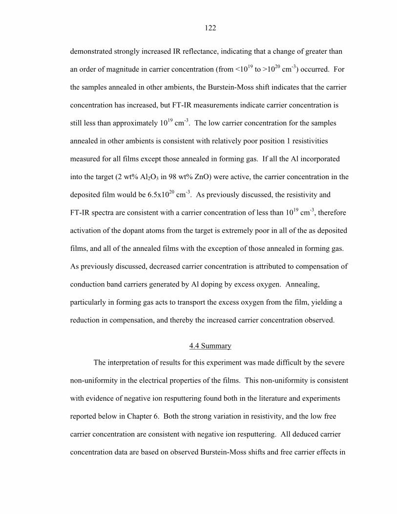
122
demonstrated strongly increased IR reflectance, indicating that a change of greater than
an order of magnitude in carrier concentration (from <1019 to >1020 cm-3) occurred. For
the samples annealed in other ambients, the Burstein-Moss shift indicates that the carrier
concentration has increased, but FT-IR measurements indicate carrier concentration is
still less than approximately 1019 cm-3. The low carrier concentration for the samples
annealed in other ambients is consistent with relatively poor position 1 resistivities
measured for all films except those annealed in forming gas. If all the Al incorporated
into the target (2 wt% Al2O3 in 98 wt% ZnO) were active, the carrier concentration in the
deposited film would be 6.5x1020 cm-3. As previously discussed, the resistivity and
FT-IR spectra are consistent with a carrier concentration of less than 1019 cm-3, therefore
activation of the dopant atoms from the target is extremely poor in all of the as deposited
films, and all of the annealed films with the exception of those annealed in forming gas.
As previously discussed, decreased carrier concentration is attributed to compensation of
conduction band carriers generated by Al doping by excess oxygen. Annealing,
particularly in forming gas acts to transport the excess oxygen from the film, yielding a
reduction in compensation, and thereby the increased carrier concentration observed.
4.4 Summary
The interpretation of results for this experiment was made difficult by the severe
non-uniformity in the electrical properties of the films. This non-uniformity is consistent
with evidence of negative ion resputtering found both in the literature and experiments
reported below in Chapter 6. Both the strong variation in resistivity, and the low free
carrier concentration are consistent with negative ion resputtering. All deduced carrier
concentration data are based on observed Burstein-Moss shifts and free carrier effects in

123
optical data taken from the film’s center (postion 1), which is the region consistently
found to have the consistently worst electrical properties. Annealing in forming gas was
found to yield resistivities much lower than any other ambient. This is consistent with a
relatively large Burstein-Moss shift of 0.3 eV and the shortest wavelength for plasma
resonance, both of which indicate larger increases in carrier concentration than for other
annealing ambients. The Burstein-Moss shift seen in spectrophotometry data from all
annealed samples suggests carrier concentration increased with all annealing ambients.
This is consistent with the decrease in electrical resistivity that occurred at position 1 for
all annealed films. No optical measurements were performed for positions 2 or 3, so
changes in carrier concentration for these positions cannot be evaluated. The decreased
resistivities found for annealing in forming gas and nitrogen would be consistent with
reduction of compensation by removal of oxygen. Oxygen annealing increases
resistivities in positions 2 and 3. It is speculated that this increase is dominated by
decreased carrier concentration, as the case for heat treatment resulting in a decrease in
carrier mobility seems implausible. Again, excess oxygen stoichiometry and
chemisorbed oxygen can both compensate conduction band electrons, therefore increased
resistivity is attributed to a combination of these two processes. The XRD results were
also taken from the center of the film, and also indicate modest improvements in the film
quality for all heat treatments. Because the changes in resistivity with different ambient
in this position were a strong function of gas ambient, while changes in the XRD spectra
were not, it is concluded that changes in crystallinity are not the dominant mechanism for
the decrease in resistivity.

124
CHAPTER 5DEVELOPMENT OF ELECTRICAL AND MICROSTRUCTURAL PROPERTIES IN
VERY THIN ZNO:AL FILMS
5.1 Background
The objective of this experiment is to investigate development of structural and
electrical properties for sputter deposited ZnO:Al thin films. The importance of this issue
is motivated by production of thinner films to decrease optical loss, to better understand
the electrical transport properties, and for the particular application of CIS based solar
cells to investigate electrical transport in the near substrate interfacial region (NSIR). For
optical loss, the intensity of transmitted light is exponentially dependent on the
absorbance (α with units cm-1) multiplied by distance the light travels in the medium (x
with units of cm) as presented in Section 2.3.3. Thus thinner films with equivalent
optical properties will absorb less light. To maintain a low series resistance for the solar
cell, the resistivity of ZnO:Al must decrease with decreasing film thickness.
Typically, structural properties of thin films are relatively poor in very thin films
during the early stages of deposition. They improve as film thickness increases. Factors
contributing to poor microstructure include small grain size, porosity, and high
concentrations of point and line defects. Investigation of relationships between structural
and electrical properties for very thin films is therefore important for solar cell
applications. Use of thinner TCO layers to increase optical transmission results in less
cross-sectional area available in the ZnO:Al layer for lateral current transport to the grid
metallization. Thus as the TCO layer becomes thinner, the more defective material near

125
the film substrate interface becomes a larger percentage of the current carrying cross-
sectional area, and plays an increasing significant role in current transport. For the case
of CIS based solar cells, there is also the issue of carrier transport across this region. The
photo-current generated in the absorber layer must cross the relatively defective region
during transport to the metallization. Optimization of TCO electrical properties typically
employs four point probe and Hall measurements of films with a thickness used for the
application. These data therefore characterize lateral transport through the “bulk” of the
thin film. To investigate electrical properties during early stages of film growth, 20 Å to
1580 Å thin films are deposited, and their structural and electrical properties are
characterized by atomic force microscopy (AFM), Auger electron spectroscopy (AES),
Hall measurements, and four point probe. Surface analysis techniques are required to
investigate the film’s structure because some of the deposited films are very thin.
5.2 Results
5.2.1 Structural Characterization
5.2.1.1 Profilometry
Profilometry measurements of thickness are difficult for films less than 100 Å,
therefore film thickness is controlled by variation of deposition time with a known
deposition rate. Deposition rate is measured by depositing a ZnO:Al thin film on a glass
substrate with a masked area. After deposition, the mask is removed, leaving a step
feature, the height of which is measured by stylus profilometry. A deposition rate of 1.75
Å/s is measured for sputter deposition conditions of 100 W RF power, 2.5 x 2.5 cm glass
substrate held off-axis from the source, a substrate to target distance of 5 cm, an Ar
pressure of 5 mTorr, and a deposition time of 900 s. Except for deposition time, all films

126
are deposited using the same conditions, and also include a 600 s presputter performed
with the deposition shutter closed. Presputtering stabilizes the source so that the
deposition rate is constant for all deposition times. Table 5-1 identifies the samples, their
deposition time, and calculated thickness. Sample 14 is used to determine deposition
rate, and therefore its thickness is measured. For the remainder of this chapter, samples
will be referred to by their film thickness, as this is the primary experimental variable.
Table 5-1. Sample indentification, deposition time, and film thickness.Sample ID Deposition Time (s) Thickness (Å)14 900 1580 (measured)16 10 1817 20 3618 60 10519 30 5420 180 31521 300 52522 420 735
5.2.1.2 Atomic force microscopy
AFM measurements are taken from small 7 x 7 mm samples cleaved from
substrate’s edge nearest the source, and used to measure the Z range, Root Mean Square
(RMS) roughness, “grain size”, and surface morphology. The Z range is the height
difference between the lowest and highest features on the sample. RMS roughness
represents the standard deviation between the height of topographic features and the
mean feature height. “Grain size” is determined by the stereological techniques
described in the Chapter 3. As was stated previously, this measurement is not expected
to give an actual grain size, but describes the diameter of distinctive granular surface
features, which may or may not reflect grain size. Figure 5-1 is a plot of the Z range,

127
0
50
100
150
200
250
300
350
400
0 100 200 300 400 500 600 700 800
Thickness (Å)
Z R
ange
& G
rain
Siz
e (Å
)
0
5
10
15
20
25
30
35
40
RM
S R
ough
ness
(Å
)
"Grain Size"
RMS Roughness
Z Range
Figure 5-1. Z range, “grain size”, and RMS roughness data for ZnO:Al thin films derivedfrom AFM measurements and plotted versus film thickness.
“grain size”, and RMS roughness derived from AFM measurements versus the film
thickness. Z range and “grain size” data use the left ordinate axis, while RMS roughness
uses the right ordinate axis. RMS roughness and Z range data from the bare glass
substrate are presented at a thickness of 0 nm.
Trends in Z range and RMS roughness data with film thickness correspond very
well. The Z range and RMS roughness are 112 and 18 Å, respectively, at a thickness of
18 Å, and decrease to 18 and 2 Å, respectively at 54 Å, then slowly and monotonically
increase to 74 and 11 Å, respectively, for the 735 Å sample. The Z range data from 18 Å
and 36Å films are remarkably higher than the calculated film thickness. Grain size data
follows similar trends to Z range and RMS roughness, but scatter in the data is larger,
with values changing from larger (330 Å) to smaller (150 Å) to larger (360 Å) for film
thicknesses of 18 Å, 54 Å, and 735 Å, respectively. Variability in “grain size” data
results from difficulty in taking micrographs for films less than 105 Å in thickness.

128
Difficulty in getting good micrographs for the thinnest films in turn causes inaccuracies
in determining the number of intersections between the line of known length and the
grain boundaries. The grain boundary intercept method [123] used to quantify “grain
size” specifies that the number of intersections with grain boundaries is inversely
proportional to grain size, therefore difficulty in measuring the number of intersections
causes a larger error in grain sizes for thinner films. In all cases, the films are very
smooth with RMS roughness less than 20 Å, and appear to be fine grained with averaged
grain sizes significantly less than 500 Å. In order to appreciate the changes that occur in
surface morphology, Figures 5-2(a-h) present the AFM micrographs used to derive
quantified surface morphology data.
Care should be used when examining the micrographs, as different z axis
sensitivities (50 to 150 Å/division) were used in the plots. The selected z axis
sensitivities were a compromise between consistency (for ease of comparison), and
different scales to accentuate the morphology. A marked difference in surface
morphology can be seen between the bare substrate (Figure 5-2a) and samples with
deposited films (Figures 5-2 (b-h)). The glass substrate has an irregular rolling hillock
surface morphology, which changes to a more defined and taller hillock surface
morphology even with the shortest deposition time. The diameter of the hillock features
associated with a deposited film change with film thickness and are what is described by
the “grain size”. For the thinnest samples (18 Å and 36 Å thick) there appears to be two
different sizes of surface features, one set with a larger height of (110 Å and 97 Å,
respectively) relatively to the smaller heights (70 Å and 50 Å, respectively). For the 18 Å
sample, the taller features are also typically larger in diameter (d~1000 Å) than the
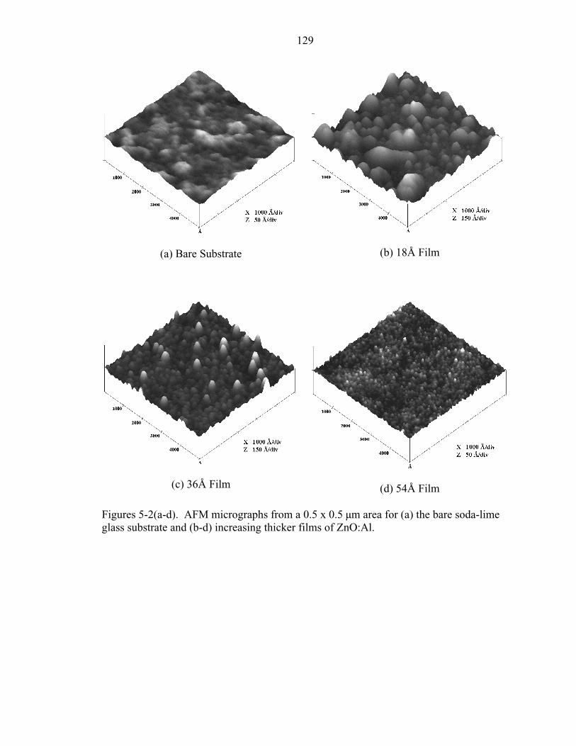
129
(a) Bare Substrate (b) 18Å Film
(c) 36Å Film (d) 54Å Film
Figures 5-2(a-d). AFM micrographs from a 0.5 x 0.5 µm area for (a) the bare soda-limeglass substrate and (b-d) increasing thicker films of ZnO:Al.

130
(e) 105Å (f) 315Å
(g) 525Å (h) 735Å
Figures 5-2(e-h). AFM micrographs from a 0.5 x 0.5 µm area for ZnO:Al thin films with(e-h) increasing thickness.
shorter features (d~100 Å). For the 36Å sample, the taller features have diameters
approximately twice (~440 Å) those of the shorter ones (~220 Å). Average grain sizes
measured by the grain boundary intercept method are 330 Å and 220 Å for 18 Å and 36
Å thick samples, respectively. For the 54 Å sample, the surface features are more
consistently the same height, but have decreased markedly in diameter to ~150 Å

131
uniformly, and subsequently increase in diameter with increasing film thickness to a
diameter of 360 Å for a 735 Å film.
5.2.1.3 Auger electron spectroscopy
Auger Electron Spectroscopy (AES) is used to characterize the surface
composition of the ZnO:Al film, changes in composition with depth into the sample by
sputter depth profiling, and composition of the substrate. From this compositional data,
stoichiometry, impurities, and percentage of the surface covered by the film are
measured. Approximate composition for soda-lime float glass is 71% silica, 16% soda,
9% lime, 3% magnesia, and 1% alumina [129]. Composition of the ZnO:Al target is
98wt% ZnO and 2wt% Al2O3, which corresponds to atomic concentrations of 48.4%,
1.6%, and 50% for Zn, Al, and O, respectively. For each sample, a survey spectrum is
collected from the as deposited sample, a sputter depth profile is continued until the Zn
signal stabilizes at the noise level, and then a final survey spectrum is collected from the
exposed glass substrate. As deposited survey spectra, sputter depth profiles, and post
depth profile survey spectra from 18 Å (thin), 105 Å (intermediate), and 525 Å (thicker)
samples are presented in Figures 5-3(a-c), 5-4(a-c), and 5-5(a-c), respectively, and
illustrate trends in the Auger data. All survey spectra are collected over the energy range
of 50 to 2050 eV. Depth profiles are plots of peak-to-peak height of differentiated signals
for selected elements as a function of Ar sputtering time.
Peaks consistent with adventitious carbon (272 eV), chlorine (179 eV), zinc (992
eV), oxygen (510 eV), aluminum (1393 eV), and silicon (1617 eV) are found in survey
spectra of as deposited samples. Adventitious carbon and chlorine show significant
variations in peak-to-peak height from sample to sample. For all samples, the carbon
signal drops off to the noise level almost immediately with sputter depth profiling

132
(a)
(b)
(c)
Figures 5-3(a-c). AES data from the 18 Å thick ZnO:Al sample with a (a) as depositedsurvey spectrum, (b) sputter depth profile, and (c) after profile survey spectrum.

133
(a)
(b)
(c)
Figures 5-4(a-c). AES data from the 105 Å thick ZnO:Al sample with a (a) as depositedsurvey spectrum, (b) sputter depth profile, and (c) after profile survey spectrum.

134
(a)
(b)
(c)
Figures 5-5(a-c). AES data from the 525 Å thick ZnO:Al sample with a (a) as depositedsurvey spectrum, (b) sputter depth profile, and (c) after profile survey spectrum.

135
suggesting it is a surface contaminant. A significant silicon peak is found in as deposited
survey spectra for 18 Å, 36 Å, and 54 Å samples. For these samples, silicon peak
intensity decreases with increasing film thickness. No silicon signal is found for 105 Å
samples, but a very small Si signal is found for 315 Å and 525 Å samples. The small Si
peak for 315 Å and 525 Å samples is unexpected, and will be discussed subsequently.
Large Zn and O peaks are found in all as deposited survey spectra. The Zn peak is
roughly half as intense as the oxygen peak for the 18 Å sample, and increases until it is
similar in intensity to the oxygen peak for samples 105 Å and greater in thickness. The
Al peak is extremely weak for some samples, and in others cannot be distinguished from
the noise level.
Sputter depth profiles of O, C, Zn, and Si signals are collected for each sample.
As indicated above, the carbon signal drops to the noise level within seconds of sputter
depth profiling. Both the deposited film and substrate contain oxygen, therefore
contributions to this signal come from the film and/or substrate. In contrast to as
deposited survey spectra from completely coalesced films (t>105 Å) where the Zn and O
peak-to-peak height is roughly equal, initially Zn peak-to-peak height is nearly two times
as intense as O in sputter depth profiles. The difference in relative peak to peak height
between Zn and O is an artifact resulting from a combination of the differentiation
algorithm and the energy step size used to collect the data. Energy step sizes of 1.0 eV
and 0.5 eV are used to collect survey and depth profile data, respectively. In each depth
profile, there is a region where the Zn signal is decreasing and Si signal is increasing,
which corresponds to the transition between taking data from the film and substrate, and
will be referred to subsequently as the transition region. For 315 Å and 525 Å films, the

136
Ar ion beam is focused on a smaller 2 x 2 mm area, as compared to a 3 x 3 mm area used
for thinner samples. Decreasing the sputtered area increases the sputtering rate such that
depth profiles can be collected over a shorter period of time. When corrected for changes
in sputtering rate, longer sputter depth profiling is needed to reach the transition region in
thicker samples. For samples 54 Å or less in thickness, which have incomplete surface
coverage, the intensity ratio of Zn to O is 1.7, 1.6, and 0.9 for 54 Å, 36 Å, and 18 Å films,
respectively. This is consistent with incomplete surface coverage suggested by the
presence of a Si peak in the as deposited survey spectra. Also, the Zn signal begins to
decrease and Si begins to increase immediately with sputter depth profiling. For all the
profiles, the double y-axis on the left side of the plots indicates that the first two data
points are taken from surfaces that have not been sputtered. Depth profiles are continued
until a short time after the Zn signal stabilizes at the noise level, to ensure the surface is
characteristic of substrate’s bulk. Shifts in peak kinetic energy up to ±10 eV from
reference values are found in some AES spectra, though smaller shifts of ±3 eV are more
typical. All peaks for the as deposited survey of 18 Å are shift approximately 10 eV
higher in energy, and this is attributed to negative charging induced by the electron beam.
A strong shift to lower kinetic energies is found with increasing sputter depth profiling
time for the 105 Å sample, but peak energies have returned to the handbook values for
the post profile survey spectra. This suggests shifts to lower kinetic energy result from
positive charging of the sample which would retard the escaping electrons.
Survey spectra taken after depth profiling generally have very few features; the
three primary peaks are two silicon peaks at 82 eV (LMM) and 1609 eV (KLL), and an
oxygen peak at 510 eV (KLL) [130]. A weak peak consistent with Ca (291 eV) is found

137
in many survey spectra after profiling, and is consistent with the glass additive of lime. A
very weak peak consistent with Mg (1183 eV) is discernable in half of the after profile
survey spectra and is consistent with magnesia added to the float glass. For the 105 Å
sample, a small peak at 990 eV after profiling is consistent with either Na or Zn, as
reference values for these peaks are within 3 eV of each other, and the peak is too weak
to extract shape information. No peak consistent with Na is found in any other case.
To approximately quantify surface coverage, the method presented in Section 3.6.2 is
applied. This method relies on the surface compositional sensitivity of AES to determine
the fraction of the surface covered by SiO2. The method takes the ratio of Si atomic
concentrations between the as deposited film and bare glass surface, which yields the
fraction of surface area which is glass. The fraction of bare substrate is subtracted from
100% to give the fraction of surface covered by ZnO:Al. Figure 5-6 plots percentage of
the surface covered by the film versus film thickness. Surface coverage is initially 60%
for an 18 Å, and rapidly increases to 100% coverage for film thickness greater than 100
Å. This procedure does not account for information volume from which the AES signal
is collected. The depth from which Auger electrons can escape while maintaining their
characteristic energies is based on the inelastic mean free path of the electron in a
material. The implications of the escape depth on the estimation of surface coverage will
be considered in the discussion.
5.2.2 Electrical Characterization
Hall and four point probe measurements are used to evaluate electrical properties
of the deposited films. Four point probe resistivity data is used to check Hall resistivity
data and investigate variations in resistivity with position on the sample. Hall

138
0
20
40
60
80
100
0 100 200 300 400 500 600 700 800
Thickness (Å)
Cov
erag
e (%
)
Figure 5-6. Percentage of the soda-lime glass substrate covered by the sputter depositedZnO:Al thin film, as derived from AES data.
measurements are used to characterize resistivity, carrier concentration, and Hall mobility
for the deposited films. Small 7 x 7 mm samples are cleaved from the substrate’s edge
closest to the sputtering source for Hall measurements. Samples with thicknesses
between 18 Å and 105 Å are too resistive to measure with either technique, which is
consistent with the lack of film coalescence measured by AES data. Based on the
minimum current and maximum voltage specifications for the instruments, 1 Ω·cm is the
highest measurable resistivity for a 100 Å film. This resistivity limit decreases linearly
with film thickness. Resistivity, carrier concentration, and Hall mobility data from 315 to
725 Å samples, and the 1575 Å sample used to determine the deposition rate are plotted
as a function of film thickness in Figures 5-7 (a-c).

139
In Figure 5-7a, resistivity starts high at 3.4x10⁻² Ω·cm for the 315 Å film, and
decreases by nearly an order of magnitude to 4.3x10⁻³ Ω·cm at a thickness of 1575 Å.
This minimum resistivity is a factor of 2 lower than the best as deposited resistivity
reported in Chapter 4. The resistivity for the 100 Å film is greater than 1 Ω·cm, and is
therefore at least an order of magnitude more resistive than the 315 Å sample. Carrier
concentrations plotted in Figure 5-7b increases by a factor of four from 6.5x10¹⁹ to
2.7x1020 cm-3 between film thicknesses of 325 Å and 1575 Å, respectively. The Al
concentration in the target is 6.5x1020 cm-3, therefore measured carrier concentrations are
between 10 and 50% of the target’s extrinsic doping concentration. Hall mobility data
are plotted in Figure 5-7c, and show values between 2.9 and 5.7 cm2/V·s for thicknesses
of 315 Å and 1575 Å, respectively. There is significant scatter in the data, and no trends
of increasing or decreasing Hall mobility with film thickness can be identified. Therefore
Hall mobility is considered to remain essentially constant with film thickness for this
experiment.
A variation of up to a factor of five in resistivity with position is measured by the
four point probe technique. Resistivity is lowest at the substrate’s edge closest to the
source, which is directly above the source’s outside edge. Resistivity increases towards
the substrate’s edge that is furthest from the source. This variation is significantly less
than the position to position variations reported in Chapter 4. Hall resistivities are within
the range of values measured by four point probe, suggesting a reasonable precision in
measurements.
140
0
0.01
0.02
0.03
0.04
0.05
0 200 400 600 800 1000 1200 1400 1600 1800
Film Thickness (Å)
Res
istiv
ity (
Ω·c
m)
(a)
0.0E+00
1.0E+20
2.0E+20
3.0E+20
4.0E+20
5.0E+20
6.0E+20
7.0E+20
0 500 1000 1500 2000
Thickness (Å)
Car
rier
Con
cent
ratio
n (c
m-3)
Target Doping Level
(b)
0
2
4
6
8
0 500 1000 1500 2000
Thickness (Å)
Mob
ility
(cm
2/V
·s)
(c)
Figure 5-7(a-c). Electrical data for ZnO:Al thin films plotted as a function of filmthickness including (a) resistivity, (b) carrier concentration, and (c) Hall mobility.

141
5.3 Discussion
5.3.1 Surface Morphology
The Z range data from AFM measurements for 18 and 36 Å samples is
significantly larger than the calculated film thickness. For the 18Å sample, the Z range is
112Å, approximately a factor of 6 larger than the estimated film thickness. For the 36 Å
sample, the Z range is 97 Å, approximately three times larger than the film thickness.
This is explained in part with hypothesis that the deposited film forms by island (Volmer-
Webber) nucleation [94]. This hypothesis is supported by the distinct change in surface
morphology between the bare glass substrate and coated substrate, and the presence of a
significant Si and Zn peaks even for a 54 Å film. Further evidence for this is the distinct
change in surface morphology in AFM micrographs and the presence of a strong Zn peak
in AES data for even the thinnest films, suggests a ZnO film is nucleating and changing
the surface properties significantly. The presence of a discernable Si peak indicates a
portion of the bare substrate is also exposed.
An island (Volmer-Webber) growth mode describes a film that does not grow
smoothly across the substrate’s surface, but instead develops small islands of deposited
material that grow both normal and parallel to the surface. Islands form because
deposited material tends to agglomerate in order to minimize the free energy of the
substrate/film/vapor system. From the capillarity theory of nucleation, which was
presented in Section 2.4.2, nucleus morphology is based on the relative surface energies
between the substrate (s), film (f), and vapor phases (v). The balance of the surface
forces is shown in Figure 2-19, and the relationship between surface tensions that yields
island growth is given in Equation 5-1 where

142
γ γ γsv fs vf< + . (5-1)
The term γ is surface tension, with subscripts describing which interface the surface
tension is associated with. If Equation 5-1 is satisfied, then the contact angle θ,
illustrated in Figure 2-19, will be greater than zero, and three dimensional or island
growth will occur. Deposited flux impinges across the whole substrate, therefore island
growth requires movement of adatoms on the surface until they join with other deposited
material to form nuclei and/or desorb as non-agglomerated material.
To determine if feature height as measured by Z range from AFM data is
consistent with island nucleation, a model involving transformation of a smooth layer to
an island layer while maintaining constant volume is calculated based on nuclei that are
modeled as half a sphere resting on the surface. An illustration of this transformation
between a smooth layer and a discontinuous layer of hemispherical nuclei is presented in
Figure 5-8. The measured deposition rate is for a film with much larger thickness than
roughness, yielding an effectively planar film. Thus the deposition rate used to calculate
film thickness assumes that a planar film results for all deposition times. The
transformation takes a 1 x 1 cm area on the substrate, with different film thicknesses
deposited on it. Film volume (Vf), from the product of area and film thickness, is set
equal to the number of nuclei (N) times nucleus volume which is a function of the
hemispheres radius (r). This relationship is expressed in Equation 5-2, and assumes
nuclei are perfect non-overlapping hemispheres of uniform size with radius r and has the
form
V N rf = ⋅ 23
3π . (5-2)

143
Substrate
radius
Initial Film TransformedFilm
Figure 5-8. Schematic representation of the constant volume transformation between asmooth layer and hemispherical nuclei.
Additionally, N hemispherical nuclei will cover a surface are of Sf, which is described by
the relationship in Equation 5-3 where
S N rf = ⋅π 2 . (5-3)
MathCAD is used to evaluate these two formulas for a series of film thicknesses, which
changes the film volume, and for each film thickness, a series of different nucleus radii
are evaluated [131]. The results are plotted as percentage of the 1cm x 1cm surface
covered by nuclei versus the nuclei radius. The colored lines represent contours of equal
film thickness, and show changes in covered surface area for different nucleus radii.
Figure 5-9a is a plot of percentage surface area covered versus nucleus radii for films
between 20 and 100 Å, and radii between 1 and 400 Å. Figure 5-9b is a similar plot, but
concentrates on films between 20 and 60 Å in thickness, and nucleus radii between 1 and
200 Å.
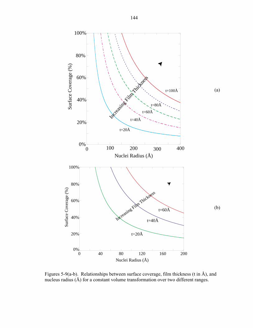
144
Nuclei Radius (Å)
Surf
ace
Cov
erag
e (%
)
100%
80%
60%
40%
20%
0%100 200 300 4000
t=20Å
t=40Å
t=60Å
t=80Å
t=100Å
Incr
easin
gFi
lmThi
ckne
ss
(a)
100%
80%
60%
40%
20%
0%0 40 80 120 160 200
Nuclei Radius (Å)
Surf
ace
Cov
erag
e (%
)
t=20Å
t=40Å
t=60Å
Increasi
ng FilmThick
ness
(b)
Figures 5-9(a-b). Relationships between surface coverage, film thickness (t in Å), andnucleus radius (Å) for a constant volume transformation over two different ranges.

145
The AES results suggest surface coverage is 60% for an 18 Å film. Looking at
the contour for a 20 Å film in Figure 5-9b, 60% coverage corresponds to a nuclei radius
of 50 Å, and a grain diameter of 100 Å. If the RMS roughness and Z range calculations
are restricted to an area where only smaller surface features are present, the Z range and
RMS roughness are 70 Å and 11.72 Å, respectively, and “grain size” is approximately
100 Å. Thus predicted feature sizes for an island layer are consistent with the smaller
features found for this sample. But the larger features which have a Z range of 112 Å and
grain size ~ 1000 Å are not consistent with this model. Interpretation of the larger
features will be discussed below. The AES results suggest surface coverage for a 36 Å
film is 70%. The model suggests a nucleus radius of 70 Å will result in 70% coverage
for a 36 Å film. The Z range is 97 Å and 50 Å and “grain size” is 440 Å and 220 Å for
large and small features, respectively. Thus the 36 Å film is similar to the 18 Å film in
that the smaller features are consistent with feature sizes predicted by the island model,
whereas the large features are larger than predicted. This suggests that the measured Z
ranges that are larger than the film thickness for 18 Å and 36 Å samples are due to island
formation during the initial stages of film deposition. For both cases, the heights of
hemispherical nuclei can be two to three times the height of a smooth layer with the same
volume.
Explanation of the larger surface features is more challenging. While the constant
volume morphology transformation gives results that are consistent with small surface
features, large surface features are still too large. Two possible explanations for the large
features are that they are simply large nuclei, possibly formed by two or more nuclei
coming together, or that these features are really exposed glass substrate. Evidence

146
against the large features being combined nuclei includes the large difference between
measured and modeled feature size, the difference in morphology between large and
small nuclei, and the lack of recognizable exposed free substrate suggested by AES
measurements. The other possibility is the large features are really exposed glass
surfaces. This is possible if the AFM tip experiences a larger repulsive force from the
exposed glass surface than the ZnO:Al film. The presence of static electricity of the same
polarity on exposed glass surfaces and the AFM tip would cause them to repel each other
and produce an image with artificially large features for area corresponding to bare glass.
Static charge would be mobile in the ZnO due to its relatively low resistivity, and
therefore it is possible that the glass substrate and ZnO film interact differently with the
AFM tip.
Even if only the smaller features are considered for 18 and 36 Å samples, these
features are large compared to the minimum in Z range and RMS roughness that occurs
for the 54 Å sample, which are 18 Å and 1.8 Å, respectively. AFM and AES results from
54 Å and thinner samples suggest that very early in deposition, roughness increases
dramatically as the deposited film forms 3D island nuclei. As deposition time increases,
nucleus density and size increases as more nuclei form and grow under the continued
flux. The additional nucleation increases coverage of the bare glass surface, and
therefore has a smoothing effect on the film morphology. As the film approaches
coalescence, the roughness approaches values measured for the bare glass substrate.
Films greater than 54 Å in thickness slowly increase in roughness, but even the
thickest film is slightly less rough than the 18 Å film. The film becomes physically
continuous at between 54 Å and 105 Å in thickness, as indicated by the lack of detected

147
silicon for 105 Å films. The 54 Å and 105 Å samples are also nearly as smooth as the
substrate, though surface morphology is still distinctly more similar to ZnO films. At this
thickness the substrate surface effectively becomes ZnO, which marks completion of
nucleation and, and is followed by film growth and development of the film’s structure
[101]. Thus the initial high but steep decreasing roughness for films between 18 Å and
54 Å results from nucleation, and with coalescence at 105 Å and for increasing thicker
films, microstructual development involves slow increasing Z range and RMS roughness.
The low but slowly increasing roughness for films thicker than 54 Å suggests that
with coalescence, further film growth involves slowly increasing feature sizes. The
process of expanding grain size in thin films results as some grains grow more quickly
than others. Slower growing grains get crowded out as faster growing grains get larger,
and start growing together. Also, large grains impede the deposited flux from reaching
small grains by a shadowing process. If a particular crystal face has a lower free energy,
this plane typically grows more quickly. This process is often responsible for
crystallographic texturing, and is describe in Section 2.4.2 in the literature review.
Preliminary samples prepared to optimize deposition conditions for best electrical
properties showed a strong basal (002) texture in XRD spectra, therefore it is likely that
samples for this experiment deposited using the same deposition conditions also have a
strong basal texture. This mechanism for grain evolution is consistent with the slowly
increasing Z range and roughness that occurs after film coalescence. The postulated
microstructural development process for ZnO:Al films will be incorporated into the
discussion of electrical properties.

148
In discussion of AES results, it is important to remember that this techniques has
very different sensitivities to different elements. AES survey spectra and depth profiles
are presented and interpreted in terms of the peak to peak height for elemental signals
present. The sensitivity factors are used to turn the raw peak to peak height of the
differentiated Auger peak into an atomic concentration. Most measurements involve
comparisons between samples, and therefore calculating atomic concentrations is
unnecessary, but it is useful to know the sensitivities for interpreting the data. For the
elements of interest, the sensitivity factors are: Zn(997 eV)=0.190, O(510 eV)=0.400,
Si(1609 eV)=0.038, C(272 eV)=0.140, and Al(1396 eV)=0.070 [130]. The relatively low
sensitivity for silicon inhibits the ability to measure small concentrations on the surface.
As previously mentioned, quantification of atomic concentrations is used for estimation
of surface coverage. Another important issue is that elemental signals never go
completely to zero for depth profiles. This is an artifact of the data collection process
used by the computer, and results from noise in the energy window. The non-zero noise
level is seen in depth profile data, but does not represent a true Auger peak height.
For Auger Electron Spectroscopy, compositional analysis and estimation of
surface coverage are both of interest. The as deposited survey spectrum for the 525 Å
sample suggests a continuous layer of ZnO, with some carbon and chlorine surface
contamination. Both contaminants are common, and mostly likely result from
atmospheric interaction and perspiration. The carbon signal quickly decays to the noise
level with depth profiling, confirming that it results from surface contamination, i.e.
adventitious carbon. There is also an extremely weak Si signal present for the as
deposited film. Because no Si peak is present in the 105 Å as deposited survey spectrum,

149
the weak Si peak from 525 and 735 Å samples is considered to result from glass dust
from the scribe and cleave procedure used to make Hall measurement and AFM samples.
Depth profile data indicates Zn and O peak to peak height are constant between 0.5 to 6
minutes of sputter depth profiling, with no C or Si beyond the noise level. Lack of C
suggests the films are free of contamination, and lack of Si indicates this region of the
depth profile represents the “bulk” of the film. After 6 minutes, the Zn signal decreases
and Si signal increases indicating the substrate is being exposed. The breadth of the
transition region between the ZnO:Al film and glass substrate is discussed below.
Spectra for all film thicknesses taken after sputter depth profiling exhibit peaks consistent
with soda-lime glass, which always includes Si and O peaks, and sometimes includes Ca
and/or Mg peaks. The presence of Na should be detected based on the sensitivity of AES
to Na, and typical concentrations used for soda-lime glass (16wt% Na2O). Depletion of
soda at the glass surface could occur through dissolution in water during the wet cleaning
process used on the glass substrate, as soda in glass is known to be water soluble [129].
Alternatively, sodium is often a mobile species in materials, and can be pushed by the Ar
ions used for depth profiling. Positive Ar ions used for sputter depth profiling would
repel positive Na ions in the material, potentially driving them deeper in the glass
substrate where they are not detected [132].
For the 105 Å sample, results are very similar to the 525 Å sample. Again, the as
deposited sample shows surface contamination by C and Cl. The carbon signal drops
immediately to the noise level with depth profiling, indicating it is a surface contaminant.
In sputter depth profile data for the 105 Å film, the Zn and O signals remain constant
between 0.5 and 3 minutes of sputter, followed by decreasing Zn signal and an increasing

150
Si signal, signifying penetration of the film such that data comes from both the film and
glass substrate. The as deposited survey spectrum from the 18 Å sample has Zn, O, C,
and Cl peaks, but also has a significant silicon peak from the glass substrate. Depth
profile data from before the first sputtering step show the Zn to O peak ratio is lower than
for 105 Å and 525 Å films, and the Si peak is larger. Also, the Zn signal intensity
dropping immediately towards the noise level with sputtering, and the lack of a constant
large Zn signal are both consistent with incomplete surface coverage. Thus for all films,
only surface contamination is present as suggested by survey spectra from as deposited
films and depth profiles. The Si signal in as deposited survey spectra for 18 Å, 36 Å, and
54 Å films is consistent with incomplete surface coverage.
The decrease in Zn intensity and rise in Si intensity takes place over a significant
portion of the total depth profile time for all films. Because the deposition process is
performed at low temperatures, reactions and diffusion between substrate and film is not
anticipated. Therefore the breadth of the film substrate interface in the depth profile data
is the result of film roughness. Both the as deposited roughness and roughness induced
by sputter erosion will broaden this region, following processes that are well described in
the literature [124,125].
5.3.2 Electrical Characterization
The best as deposited resistivity measured in this experiment is 4.3x10⁻³ Ω·cm,
which is roughly a factor of 3 lower than the best as deposited resistivity reported in
Chapter 4. This improvement in as deposited resistivity is attributed to holding the
substrate off-axis of the source, which prevents negative ion resputtering of the deposited
film. It was postulated that the consistently larger resistivities reported for Position 1 in
Chapter 4 resulted from negative ion resputtering. Optical data indicated that the high

151
resistivity resulted from very low carrier concentrations (n<1019 cm-3). The lowest carrier
concentration measured for this experiment is 6.5x1019 cm-3, which suggests negative ion
resputtering increases resistivity by decreasing carrier concentration. This agrees with
results reported below in Chapter 6, which is a more detailed investigation of negative
ion resputtering.
Hall data show some interesting and non-intuitive trends with film thickness. As
a first approximation for predicting the changes in electrical properties for very thin
films, the ZnO:Al film can be considered metal-like. Two of the leading theories treating
the electrical properties of thin continuous metal films were developed by Fuchs and
Sondheimer [133,134], and Mayadas and Shatzkes [135]. A simple expression for
resistivity (ρ) in the very thin film regime is given in Equation 5-4 [136] where
ρρ
F
B
l
tp= +
−( )1
38
1 . (5-4)
The subscripts on the resistiviy indicate bulk (B) and film (F), respectively. The term p
describes interactions between carriers and the free surfaces, is a unitless variable, and
has values from 0 to 1. If P=1 then carriers are specularly reflected from the interfaces,
and therefore they do not influence resistivity. If P=0, carriers interacting with free
surfaces are diffusely scattered, and therefore free surface interfaces decrease carrier
mean free path and increase resistivity. The term (l/t) is the ratio of the film thickness to
the mean free path of the carriers. This term indicates that for surface scattering to be
important, the film thickness must be equal to or thinner than the length of the carriers
scattering mean free path. A schematic illustration of this model is presented in Figure
5-10. The first (1) arrow indicates the “bulk” mean free path of the carrier (l). The
second (2) arrow illustrates a carrier that is specularly reflected from the film surface, and

152
therefore maintains the same direction and mean free path. The third (3) arrow illustrates
a diffuse scattering event where the carriers mean free path is significantly shortened. A
plot of the theoretically predicted trends in the ratio of ρF to ρB with different p values is
shown in Figure 5-11 [137]. This plot shows a similar trend to the resistivities measure
in the deposited ZnO:Al films. As the film thickness increases, the resistivity decreases
exponentially towards a minimum value (Figure 5-7a). This model implicitly assumes
that resistivity changes in very thin films result from increased carrier scattering.
Therefore this model predicts as thickness decreases, scattering and therefore resistivity
increases.
The Hall data presented in Figure 5-7c reveal a disagreement with the Fuchs and
Sondheimer model. Resistivity does decrease in a manner consistent with this model, but
the mechanism causing this decrease is reduced carrier concentration, not reduced mean
free path or mobility (Figures 5-7 b and c). No trends for increasing or decreasing
mobility with film thickness is observed. Carrier concentration is observed to decrease
by a factor of 4 from 2.7x10²⁰ to 6.5x1019 cm-3 with decreasing film thickness from 1575
Å to 325 Å. Decreasing carrier concentration correlates with increasing resistivity for
decreasing thickness, with resistivity increasing by a factor of 8 from 4.3x10⁻³ to 3.4x10⁻²
Ω·cm from 1575 Å to 325 Å. This suggests increasing resistivity with decreasing film
thickness is dominated by decreasing carrier concentration.
Indirect evidence suggests resistivity continues to increase with decreasing film
thickness. The AES data suggests that the 105 Å sample is a completely coalesced film.
Based on the measurement range of the Hall and four point probe instruments, the
maximum measurable resistivity for a 105 Å sample is ~1 Ω·cm. Therefore the 105 Å

153
Substrate
ThinFilm
l 12 3
Figure 5-10. Illustration of carrier trajectories based on the Fuchs and Sondheimer modelwith (1) bulk transport, (2) specular reflection from the interface, and (3) carrierscattering at the interface.
Figure 5-11. Calculated plot of the resistivity ratio between the thin films with interfacescattering and bulk films as a function of mean free path (l), film thickness (t), andinterface character (p), with larger numbers being more specular in carrier reflection.
154
sample’s resistivity is some value greater than 1 Ω·cm, which is at least 30 times larger
than the value of 3.4x10⁻² Ω·cm found for 315 Å. The AFM and AES data suggest 54 Å
and thinner films are not coalesced and are increasing in roughness with decreasing
thickness. The mechanism of conduction in a noncoalesced film is fundamentally
different, but the percolation mechanism is beyond the scope of interest for this
experiment.
An alternate mechanism to explain the increased resistance in thin films is
postulated. In this mechanism, chemisorbed oxygen species decrease the carrier
concentration with decreasing film thickness in coalesced films. While metals
fundamentally have free mobile electrons due to metallic bonding, ZnO:Al depends on
donor states generated by defects to achieve free electron carriers. The Al doping level of
the target is 6.5x1020 cm-3, which indicates that even with 100% incorporation, the free
electron concentration of these films are roughly two orders of magnitude lower than a
typical metal. This lower carrier concentration leaves very thin films vulnerable to
compensation by trapping of conduction band electrons on chemisorbed oxygen.
Mechanisms for oxygen chemisorption and its effect on carrier concentration for ZnO are
presented in the literature review section discussing ZnO as a thin film sensor for
particular gases (section 2.3.2). To evaluate the potential of chemisorbed oxygen to
decrease carrier concentration, some simple modeling is performed. For the 325 Å film,
the carrier concentration is only 10% of the Al dopant concentration in the target, which
suggests that enough oxygen must be chemisorbed to remove up to 90% of the free
carriers in the film. To further simplify the calculation, the quantity of carriers in the
film, which is the product of the carrier concentration (n=6.5x1020 cm-3) and the film

155
thickness (t), is set equal to the density of available surface sites (S) (typically ~1015
cm-2). Assuming a planar surface saturated with chemisorbed oxygen, a film up to 150 Å
would be completely compensated. This is in reasonably agreement with the level of
depletion found for the 325 Å film, and is consistent with the rapidly decreasing carrier
concentration with decreasing thickness. The presence of grain boundaries in the
polycrystalline film, the interface with the substrate, and surface roughness provide
additional area for chemisorption, which increases the possible fraction of compensation.
The likelihood of a surface saturated with chemisorbed oxygen species is small, which
lowers predicted compensation. This mechanism is also consistent with decreasing
carrier concentration with film thickness found in experimental data reported in Chapter
6, which will be discussed using a similar model.
This model can also explain variations in resistivity found by four point probe
data across the surface. The entire 2.5 x 2.5 cm substrate is positioned off the targets
normal axis. Lowest resistivities are found for areas closest to the sputter source, which
are positioned above the outside edge of the source. Resistivities increase with position
towards the edge of the substrate furthest from the source’s center. The non-uniform flux
distribution will result in decreasing film thickness on the substrate further from the
source’s center. For very thin films, decreasing film thickness with position on the
substrate further from the deposition source results in increased compensation and
therefore increased resistivity. Also, film thickness was measured near the substrate’s
edge closest to the source’s center, therefore the film is thinner than measured for areas
farther from the source’s center. Measured thickness is entered into Equation 3.2, which
is used to calculate resistivity from measured current, voltage, and film thickness. If the
156
actual film thickness is less than the measured film thickness, then the derived resistivity
is higher than the actual value. A combination of both effects is considered responsible
for variations in resistivity across the substrate.
5.4 Summary
Both the microstructural and electrical properties of sputter deposited ZnO:Al thin
films are found to evolve significantly with increasing thickness. The microstructural
evolution consisted of changes in surface morphology, Z range, RMS roughness, “grain
size”, and surface coverage as measured by AFM and AES. The thinnest films (0 to 40
Å) are found to be discontinuous, and had a remarkably high Z range and RMS roughness
compared to the substrate. Features of two different sizes appear in the micrographs. For
the 18Å and 36Å films, the smaller features have a 70Å and 50Å Z range, respectively,
which is still significantly larger than film thickness. A simple model to predict the
effects of islands on feature height suggests that the smaller features are three
dimensional nuclei. The large features are much too large to be predicted by the island
model. These features are attributed to static electric interactions between the glass
substrate and the AFM tip. AES data indicates 54 Å films are still not continuous, but
surface coverage has increased to approximately 80%. The Z range and roughness also
decreased significantly, approaching the values for the glass substrate. Films become
continuous at thicknesses between 50 Å to 100 Å, and a steady trend of increasing
roughness, decreasing resistivity, and increasing carrier concentration is observed with
increasing thickness. The “grain size” is used to quantify the diameter of surface
features, which might or might not represent individual grains of the polycrystalline film.
The “grain size” follows similar trends as Z range and RMS Roughness, albeit with more

157
scatter in the data. AFM and AES data are consistent with island (Volmer-Webber)
nucleation and growth. The slow increase in “grain size” with film thickness for
coalesced films (t>100 Å) is attributed to differences in grain growth rates due to
shadowing and free energy of the growth surface. XRD spectra from preliminary
samples used for optimization of electrical properties indicate (002) texturing occurs in
samples deposited by the sputter deposition process used.
The electrical properties also change significantly in this film thickness regime.
The resistivity decreases sharply as the film thickness increases. Measured values range
over an order of magnitude, with a minimum resistivity of 4.3x10⁻³ Ω·cm for as deposited
films. This improved resistivity as compared to as deposited samples in Chapter 4 is
attributed to lack of negative ion resputtering, due to use of the off-axis deposition
geometry. Films which are discontinuous (18 Å < t < 54 Å) have resistivities too high to
measure. The AES data suggest that the 105 Å film is continuous, but the resistivity
remains too high to be measured. As film thickness increases, the resistivity decreases in
a manner consistent with the Fuchs and Sondheimer model for conduction in very thin
metallic films, which specifies that resistivity increases with decreasing film thickness
due to increased scattering from interfaces. Carrier concentration and Hall mobility data
indicate that the mechanism responsible is different than the Fuchs and Sondheimer
model, as carrier concentration is responsible for a majority of the change in resistivity.
The carrier concentration decreases by a factor of 4 from 2.7x10²⁰ to 6.5x1019 cm-3 with
decreasing thickness from 1575 Å to 315 Å, and is therefore primarily responsible for the
increase in resistivity. The proposed mechanism for decreasing carrier concentration
with film thickness is postulated to be increasing compensation due to chemisorbed

158
oxygen species. This mechanism is supported by a simple model which indicates that for
very thin films, the quantity of free carriers becomes similar to the number of sites
available for oxygen chemisorption. Therefore, as film thickness decreases with a
concomitant decrease in the total number of conduction band electrons, the quantity of
chemisorbed oxygen remains roughly the same due to equivalent free surface and grain
boundary area in the film. This results in an increasing fraction of the available electrons
being consumed by chemisorption of oxygen species, reducing the film’s carrier
concentration.
159
CHAPTER 6NEGATIVE ION RESPUTTERING
6.1 Background
Negative ion resputtering (NIR) has been postulated to have a strong influence on
the electrical properties of sputter deposited ZnO:Al thin films from earlier experiments
within this work and from reports in the literature [101,109,112,113,116]. Despite the
strong influence, there is a lack of detailed information regarding this process and its
effects on developing films. The experiment presented in this chapter investigates the
magnitude of NIR effect on structural and electrical properties, how RF power influences
this process, and mechanisms by which the electrical and structural properties of the films
are affected. The relative magnitude of the effect is evaluated by characterization of
electrical and physical properties of the deposited films. This introduction is followed by
presentation of results from electrical and physical characterization, discussion of the
results, and a summary of critical findings.
The process of negative ion resputtering (NIR) is described in section 2.4.3 of this
work. The process involves generation of a negative ion in close proximity to the
sputtering source (cathode), with the ion being accelerated away from the source by the
same electric field that attracts positive Ar ions towards the target for the sputtering
process. Negative oxygen ions (O-) are responsible for NIR during sputter deposition of
ZnO, and are accelerated to a significant portion of the cathode potential which varies
between -300 to –1000 V DC with RF power used in this study. Thus, the negative
160
oxygen ions are accelerated to similar energies as the Ar+ in the sputtering process, and
can therefore cause damage and resputtering to the deposited film. Previous unreported
experiments from this work, and reports in the literature [76,111,112] suggest the
negative ion flux is highly directional, with the ions being accelerated perpendicularly
away from the target’s surface. For magnetron sources, the negative ion flux is found to
be most intense in areas directly opposed to the racetrack erosion region of the target.
Experimental evidence for this is seen in the strongly position sensitive electrical
properties of deposited films discussed in Chapter 4. Often the best film properties are
obtained for substrates supported off-axis from the target’s normal axis in the manner
used for experiments in Chapter 5 and/or with the substrate perpendicular instead of
parallel to the sputtering target. This is consistent with decreased minimum resistivity for
as deposited samples from Chapter 5 compared to Chapter 4, and several reports in the
literature which also find off-axis deposition geometry to improve electrical properties
[76,111].
Process parameters that influence the NIR must be determined to investigate this
effect. Based on the postulate that the NIR effect is very position dependent, the
properties of a film deposited across a large substrate are measured in an initial
experiment. Strong variations of the resistivity with position on the substrate were
measured, in a pattern consistent with NIR. Therefore, variations in properties with
position can be used to evaluate the NIR effect. The influence of RF power is the process
variable investigated in this way.
Parameters held constant across these experiments include use of the same sputter
deposition system and target. The substrate and its position are also held constant. Three

161
2.5 x 5 cm glass substrates side by side effectively formed a 2.5 x 15 cm substrate. This
substrate was 9 cm below the target, with one edge below the target’s center, which is
defined as 0 cm. This geometry is detailed in the experimental methods section, and is
schematically represented in Figure 6-1. One exception to this geometry is the 500 W
sample, which was deposited in a preliminary experiment. This substrate is positioned
away from the target’s center towards the target’s edge. Based on trends in the data and
memory of placing the sample in the system, it is estimated that the substrate was
translated ~3.2 cm radially away from the center of the target. As reported in the
experimental methods, there is a uniformity shield positioned below the deposition
source, which influences deposition rate and variations in properties induced by NIR.
The deposition parameters varied for this experiment are the RF power and deposition
time.
0 cm 5 cm 10 cm
Deposited NeutralsNegative O Ions
1.6 cm
9 cm
ZnO:Al Target
GlassSubstrate
Position
Flux
Figure 6-1. Cross-sectional view of the sputter deposition geometry, and a schematicrepresentation of the changes in deposited neutral and negative ion flux as a function ofposition.

162
6.2 Experiment Results
6.2.1 Profilometry
Profilometry across a shadowed step feature is used to measure the film thickness
at seven equally spaced points along the 5 cm dimension of the 2.5 x 5 cm substrates.
These measurements are used to characterize variations in film thickness versus position
relative to the center of the sputter deposition source. To investigate the influence of RF
power, the conditions used to deposit the samples are 250 W and 500 W for 60 minutes,
and 1000 W for 20 minutes. The thickness and deposition rate as a function of position
on the substrate for the three RF powers are presented as in Figures 6-2 and 6-3,
respectively. In each of these plots, there are two curves associated with the 500 W
deposition condition. The dashed line represents data mathematically offset by adding
3.2 cm to the positional index to make zero consistently the center of the source for all
three RF power conditions. Data with the position index manipulated in this way will be
referred to as offset data, and an offset of 3.2 cm will be used consistently. As a reminder
of the offset, 500 W data plotted versus position will always be plotted with a dashed
line. The solid line represents the actual data, with the positional index relative to the end
of the substrate, and not the center of the sputter deposition source. The offset 500 W
data is used in the following results and discussion sections. Any reference to data
without the offset will be referred to explicitly as non-offset data. The red dashed vertical
markers designating positions of the regions apply to the offset data for samples
deposited at 500 W, and the data for samples deposited at 250 W and 1000 W.
The thickness and deposition rate of the deposited films span more than an order
of magnitude between the ends of each substrate. The thinnest measured films are
approximately 100 Å thick. This limit is imposed by the lack of optical contrast needed

163
0
2000
4000
6000
8000
0 2 4 6 8 10 12 14
Position (cm)
Thi
ckne
ss (
Å)
1000 W
500 W
250 W
500 W (Offset)
Region I Region II Region III
Figure 6-2. Measured thickness of the ZnO:Al thin film as a function of position on thesubstrate and RF power used to deposit the film.
0.0
1.0
2.0
3.0
4.0
5.0
0 2 4 6 8 10 12 14
Position (cm)
Dep
ositi
on R
ate
(Å/s
)
1000 W
500 W
250 W
500 W (Offset)
Region I Region II Region III
Figure 6-3. Deposition rate of ZnO:Al as a function of position on the substrate and RFpower used to deposit the film.

164
to find the step feature and lack of measurement accuracy for films thinner than 100 Å.
The second of the three side-by-side substrates ends at 10 cm for the 250 W and 1000 W
cases, and 13.2 cm for the 500 W case. Only two and three data points from the 250 W
and 1000 W conditions, respectively, are taken from the third substrate, and all values
indicate very thin films. The curves for thickness and deposition rate from each power
condition show similar though offset decaying functions with increasing position. Note
the lack of intersections between the curves for different RF power conditions for either
film thickness or deposition rate. Note also that neither the thickness nor deposition rate
curves are completely smooth. Particularly strong deviations occur in the 250 W and
1000 W data around the position of 6 cm.
The molecular deposition flux, or the flux of material that contributes to the film
thickness, is calculated from the deposition rate of the film, the density of ZnO, and its
molecular weight. The flux is presented in Figure 6-4, and ranges in values between
1.5x10¹³ to 1.6x10¹⁵ molecules/cm2·s as a function of the RF power used to deposit the
film, and the position on the substrate. The trends in the flux data are identical to those in
the data for the deposition rate because the flux is calculated using a linear relationship to
the deposition rate.
One difference between the thickness and deposition rate plots is the vertical
order of the curves. The thickness of films deposited at 500 W is greater than for 1000
W, and least for 250 W. For the deposition rate, the order is 1000 W, 500 W, and 250 W
for highest to lowest, respectively. As a rule of thumb, deposition rate increases linearly
with power, all else being equal. To determine if this rule of obeyed, the ratio of the
deposition rates for the 250 W and 500 W conditions to the 1000 W condition are plotted

165
0.0E+00
2.0E+14
4.0E+14
6.0E+14
8.0E+14
1.0E+15
1.2E+15
1.4E+15
1.6E+15
1.8E+15
0 2 4 6 8 10 12 14
Position (cm)
Mol
ecul
ar F
lux
(mol
ecul
es/c
m2·s
)1000W
500W
250W
Region I Region II Region III
Figure 6-4. Deposited molecular flux of ZnO:Al plotted as a function of position on thesubstrate and RF power.
versus position in Figure 6-5. For positions less than 4 cm, the 250 W/1000 W data has a
value of ~0.23, which is very close to the expected value of 0.25. Deviations to lower
values occur between the positions of 4 and 8 cm, with the lowest value being 0.14. The
500 W/1000 W data start with value of ~0.57 around the position of 4 cm, and decrease
to values near 0.45 from ~6 to 10 cm. The final two data points are near 0.37.
6.2.2 Electrical Characterization
Electrical measurements are made using a four point probe and Hall measurement
system. The four point probe measurements are made while the substrate is still whole.
The probe head is brought down on accurately measured locations in the manner
described in section 3.3.2. Data are collected every 0.6 cm, yielding a series of 14-18
measurements from each substrate. Hall measurements are taken by the van der Pauw
method from the Hall system described in section 3.3.1, which accepts a maximum

166
0
0.2
0.4
0.6
0.8
0 2 4 6 8 10 12 14
Position (cm)
Rat
ioed
to 1
000W
Sam
ple
250W
500W
Figure 6-5. Deposition rate ratio between 250 W/1000 W and 500 W/1000 W conditionsversus position on the substrate.
sample size of 7 x 7 mm [121]. Both Hall and AFM samples were cleaved from XRD
specimens after spectra are collected. Because exact positions of Hall and AFM samples
are unknown and film thickness changes with position, there is uncertainty in the
thickness used to derive resistivity from Hall data. Inaccuracies in position are indicated
by ordinate error bars, while abscissa error bars indicate estimated error in the measured
values.
All resistivity data are plotted on semi-log axes. The resistivity as a function of
position measured by both four point probe and Hall is presented in Figure 6-6. The
mathematical offset has not been applied to the 500 W data in this plot. The solid and
dashed traces of the same color indicate four point probe and Hall data, respectively.
Resistivity data from four point probe are replotted in Figure 6-7, with the position offset
applied to 500 W data. There is good agreement between trends in resistivity for all

167
0.001
0.01
0.1
1
10
0 2 4 6 8 10 12 14
Position (cm)
Res
istiv
ity (
Ω·c
m)
500W 250W 1000W
4 Point ProbeHall Measuremet
Figure 6-6. Resistivity of ZnO:Al thin films collected by four point probe (solid) andHall measurements (dashed) versus position on the substrate and RF power.
0.001
0.01
0.1
1
10
0 2 4 6 8 10 12 14
Position (cm)
Res
istiv
ity (
Ω·c
m)
500W
250W
1000W
Region I Region II Region III
Figure 6-7. Resistivity of ZnO:Al thin films with 500 W data offset by 3.2 cm as afunction of position on the substrate and RF power from four point probe.

168
samples, and therefore remaining data will be plotted by default with the position offset
applied.
Resistivities span ~3.5 orders of magnitude for all power conditions. The general
trends for all three RF powers indicates that there are three distinct regions in the
resistivity, defined as Regions I, II, and III. Region I occurs for positions less than 4.5
cm, and has an intermediate resistivities between ρ~5x10⁻³ and ~10-1 Ω·cm. Resistivities
for 250 W samples trend from 3.3x10⁻³ up to 7.0x10⁻³ Ω·cm between positions of 0.6 to
4.5 cm. For 1000 W samples, resistivities in Region I consistently have a value near
1.3x10⁻² Ω·cm. Thus the 1000 W samples are between 2.5 and 5 time higher in resistivity
than 250 W samples. Note that the first datum point for the 500 W sample is 3.8 cm,
which is near the edge of this region. Resistivities for these samples are 2.5x10⁻² and
1.1x10⁻² Ω·cm at positions of 3.8 and 4.5 cm, respectively. Resistivity sharply decreases
by between ~4x and 8x with increasing positions from 4.5 to 5.7 cm for all RF powers,
and marks the transition between Regions I and II.
Region II spans ~5.7 to ~8 cm, and has the lowest resistivity, which is
consistently ρ~1.5x10⁻³ Ω·cm and is independent of RF power. This resistivity is
between a factor of ~5x and 20x lower than the highest resistivities from Region I. At the
8.2 cm position, resistivities increase, and significant differences between power
conditions are found, with values of 4.1x10⁻³, ~2.0x10⁻³, and 2.5x10⁻³ Ω·cm for 250 W,
500 W, and 1000 W samples, respectively. This area is the transition between Regions II
and III. The end of Region II is defined as where the resistivity starts to increase, which
occurs at the position of ~8 cm for the different RF powers. The transition between
Region II and III is not well defined in position because Region III is defined in terms of

169
film thickness, therefore its location can vary in position based on sputter deposition
conditions.
Region III corresponds to areas less than 500 Å in thickness, and has resistivities
that increase sharply with increasing position from low values of ~5x10⁻³ Ω·cm to the
highest resistivities measured in this experiment of greater than 100 Ω·cm (the maximum
measurable resistivity). Figure 6-8 is a plot of resistivity as a function of film thickness,
and shows an almost direct overlap of resistivities for samples thinner than 500 Å
indicating independence from RF power. Note that while Region III corresponds to films
less than 500 Å thick, the transition from Region I to II varies from 1000 Å to 2000 Å to
4000 Å for films deposited at 250 W, 1000 W, and 500 W, respectively. This is
consistent with the lack of correlation in resistivity plotted as a function of thickness for
Region I and the transition into Region II. Because Region III is defined in terms of film
0.001
0.01
0.1
1
10
0 1000 2000 3000 4000 5000 6000 7000
Film Thickness (Å)
Res
istiv
ity (
Ω·c
m)
500W
250W
1000W
Figure 6-8. Resistivity of the deposited ZnO:Al thin film plotted versus thickness and RFpower used to deposit the film.

170
thickness, its position on the substrate depends on deposition conditions i.e. deposition
time and RF power. Samples with a thickness of 500 Å (the beginning of Region III)
occur at 8.3, 10.2, and 8.9 cm for 250 W, 500 W, and 1000 W samples, respectively, and
all have resistivities near 5x10⁻³ Ω·cm.
Hall data are used to determine majority carrier type, carrier concentration, and
Hall mobility. All films are n-type, with carrier concentrations presented as functions of
position and film thickness in Figures 6-9(a and b), respectively. Carrier concentrations
on the order of 1020 cm-3 are needed for a TCO with a resistivity near 10-4 Ω·cm while
maintaining greater than 85% transmittance, which are requirements for high efficiency
solar cells [11,82]. This condition is met by a majority of samples with some notable
exceptions presented below. General trends in carrier concentration are low values for
Region I which increase abruptly to the highest measured values in Region II, and
decrease sharply across Region III. These trends are consistent with trends in reported
resistivity data. In Region I carrier concentrations range from 7.2x10¹⁹ to 3.3x1020 cm-3,
and have a strong dependence on RF power. The 250 W samples consistently have the
highest carrier concentrations for Region I, with values that decrease in carrier
concentration from 3.3x10²⁰ to 1.8x1020 cm-3 between positions of 0.8 and 4.2 cm.
Carrier concentration for the 1000 W samples increases from 7.2x10¹⁹ to 1.4x1020 cm-3
between 0.8 and 4.2 cm. The singular datum point for the 500 W sample in Region I has
a carrier concentration of 8.2x1019 cm-3 at a position of 4.0 cm. Note that carrier
concentrations less than 1020 cm-3 are found for the 500 W sample at a position of 4.0 cm,
and for 1000 W samples at positions of 0.8 and 2.4 cm.

171
0.00E+00
2.00E+20
4.00E+20
6.00E+20
8.00E+20
1.00E+21
0 2 4 6 8 10 12 14
Position (cm)
Car
rier
Con
cent
ratio
n (c
m-3)
1000W
500W
250W
Target Doping Level
Region I Region II Region III
(a)
0.00E+00
2.00E+20
4.00E+20
6.00E+20
8.00E+20
1.00E+21
0 1000 2000 3000 4000 5000
Film Thickness (Å)
Car
rier
Con
cent
ratio
n (c
m-3)
1000W
500W250W
Target Doping Level
(b)
Figure 6-9(a-b). Carrier concentration of ZnO:Al thin films from Hall measurements andplotted versus (a) position on the substrate and (b) film thickness.

172
Carrier concentrations increase sharply (2 to 4x) for the transition between
Regions I and II at positions from 4 and 6 cm, and reach maximum into Region II where
all values are greater than 1020 cm-3. For 250 W samples, carrier concentration decreases
across Region II from 4.9x10²⁰ to 2.7x1020 cm-3 at positions of 5.9 to 7.6 cm. The 500 W
samples exhibit consistent values near 4.0x1020 cm-3 across Region II from positions of
5.7 to 9.1 cm. For 1000 W samples, carrier concentration increases across Region II
from 5.4x10²⁰ to 7.6x1020 cm-3 at positions of 5.8 and 7.6 cm.
The plot of carrier concentration versus position indicates that carrier
concentrations are lower in Region III than Region II. Looking at carrier concentration
as a function of film thickness, it is important to note that for 250 W and 1000 W data
there is only one datum point from Region III, therefore there are no trends in data within
this region. Also note that no abscissa error bars are present for data plotted as a function
of thickness. This is because errors are estimated in terms of position, and position is not
linear when plotted as a function of thickness. For the 250 W sample, carrier
concentration is 2.3x1020 cm-3 for a film thickness of 300 Å at a position of 9.3 cm. The
carrier concentration is within experimental error of value taken from the position of 7.6
cm from Region II. For 500 W samples, a decrease of more than an order of magnitude
in carrier concentration occurs with thickness from 1.5x10²⁰ to 1.0x1019 cm-3 with film
thicknesses from 350 Å and 200 Å, respectively. For the singular 1000 W data point in
Region III, the carrier concentration is 1.9x1020 cm-3 for a film thickness of 500 Å and a
position of 9.3 cm. Carrier concentration is ~4 times lower than the adjacent value from
position 7.6 cm from Region II. Note that the carrier concentration for 500 W sample
with a thickness of 200 Å has a carrier concentration an order of magnitude lower that
173
1020 cm-3. Additionally, all positions with carrier concentrations less than 1020 cm-3 are
also marked with red data markers in quantified XRD results. The meaning of the red
data markers will be presented in the XRD results section, and implications of this
correlation will discussed below.
With the exception of one datum point (1000 W at 7.6 cm), all carrier
concentrations are below the Al doping concentration of the target (6.5x1020 cm-3). The
highest carrier concentrations for the 250 W, 500 W, and 1000 W samples are 4.9x10²⁰,
4.4x10²⁰, and 7.6x1020 cm-3, respectively. These carrier concentrations are 69%, 75%,
and 116%, respectively, of the target’s extrinsic doping concentration. While these
carrier concentrations are good, they are the highest values measured. The worst dopant
activation percentages measured from Region I for the 250 W, 500 W, and 1000 W cases
are 28%, 13%, and 11% respectively. Note that the 500 W sample also shows an
exceptionally low carrier concentration of 1.04 x1019 cm-3 at 12.5 cm in Region III,
which translates to less than 2% activation.
Hall mobility is plotted as a function of position and film thickness in Figures
6-10(a-b). The highest mobility is < 12 cm2/V·s, which is approximately half the value of
a high quality ZnO TCO (µ>25 cm2/V·s) [28]. There is not a strong correlation between
Hall mobility and position or deposition power. The Hall mobility data will be discussed
versus RF power instead of by position. For 250 W samples, there is a 25% increase
between the worst (6.4 cm2/V·s) and best (7.9 cm2/V·s) Hall mobility in Regions I and II
(positions < 8 cm), which about the precision of the measurement. For 1000 W samples,
there is a 55% increase in mobility between the worst (4.7 cm2/V·s) and best (8.0
cm2/V·s) mobility in Regions I and II, which indicates at least a small variation

174
0
4
8
12
16
0 2 4 6 8 10 12 14
Position (cm)
Mob
ility
(cm
2/V
·s)
1000W
500W
250W
Region I Region II Region III
(a)
0
5
10
15
0 1000 2000 3000 4000 5000
Film Thickness (Å)
Hal
l Mob
ility
(cm
2/V
·s)
1000W
500W
250W
(b)
Figures 6-10(a-b). Hall mobility of ZnO:Al thin films plotted versus (a) position on thesubstrate and (b) film thickness.

175
beyond the uncertainty of the measurement. The trends in data decrease from 7.3 to 4.7
cm2/V·s between 0.8 and 4.2 cm across Region I. It then increases across Region II to a
value of 8.4 cm2/V·s at 7.6 cm. The mobility of both 250 W and 1000 W samples
decrease sharply at 9.3 cm in Region III with values of 2.2 and 3.0 cm2/V·s, respectively.
The 500 W samples show the largest variation in mobility with an 87% decrease
from best (12 cm2/V·s) to worst (1.5 cm2/V·s) at positions of 5.7 and 12.5 cm,
respectively. Between Region I and II (4.0 and 5.7 cm), the change is less than the
uncertainty of the measurement. From 5.7 cm (highest mobility) to 12.5 cm (lowest
mobility), the data decreases monotonically and the change is greater than the
measurement error.
No systematic correlation between mobility and film thickness is found for the
different RF powers for films thicker than 1000 Å. Below approximately 600 Å, the
mobility of all samples decreases with fairly consistent slope and similar magnitudes.
This indicates a correlation between thickness and mobility that is independent of the
deposition power in Region III.
6.2.3 Secondary Ion Mass Spectrometry Results
The composition of the deposited ZnO:Al thin films is characterized by secondary
ion mass spectrometry (SIMS). The SIMS data is collected from the Hall measurement
sample, and the Al dot contacts used for Hall measurements are carefully avoided.
Elements of interest include Zn, Al, and the alkali metals, which are electropositive
elements; therefore results are collected with an oxygen primary beam using the
conditions specified in section 3.4.6. The presented results are SIMS depth profiles taken
using dynamic SIMS techniques. The plotted data are the intensity ratios of Al to Zn and
Na to Zn as a function of sputtering time, with different positions indicated by the
176
different colored lines. Multiple lines of the same color show replicate data, which is
useful to evaluate the measurement error in the data. The Al to Zn and Na to Zn data for
250 W, 500 W, and 1000 W data are presented in Figures 6-11(a-b), 6-12(a-b), and 6-
13(a-b), respectively. No standard compounds were available, therefore only qualitative
analysis could be performed. The qualitative measurements are repeatable, which allows
accurate comparison between data from different positions on the substrate.
The ratio of Al to Zn was found to be consistently between 0.015 and 0.045 for all
samples from 250 W, 500 W, and 1000 W deposition powers when the large features at
the beginning and/or end of the depth profile are neglected. This indicates that a factor of
three is the maximum variation in the Al to Zn ratio that occurs. The consistent increase
in the Al to Zn ratio at longer sputtering times likely results from the presence of alumina
additive and lack of any zinc compounds in the float glass substrate. Data from samples
deposited at 250 W show no change in the Al to Zn ratio as a function of position. For
samples deposited at 500 W and 1000 W, the Al to Zn ratio is consistently higher in
Region I compared to Region II, indicating areas receiving a negative ion flux had
slightly higher Al concentrations. In all cases an almost direct overlap in data is found
when more than one depth profile is collected from a sample.
Values for the Na to Zn ratio range from 0.04 to 0.2 for 250 W data, 0.1 to 0.4 for
500 W data, and 0.035 to 0.1 for 1000 W data. There are also sharp increases at the
beginnings and ends of the depth profiles, and result from Na contamination of the film’s
surface for the high ratios early in the profile, and presence of soda in the glass substrate
for longer times in the depth profile. Though precise values for relative sensitivity
factors (RSF) are not known due to the lack of standards, generally the RSF increases
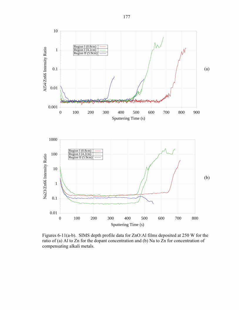
177
0.001
0.01
0.1
1
10
0 100 200 300 400 500 600 700 800 900
Sputtering Time (s)
Al5
4/Z
n66
Inte
nsity
Rat
ioRegion I (0.8cm)Region I (4.2cm)Region II (5.9cm)
(a)
0.01
0.1
1
10
100
1000
0 100 200 300 400 500 600 700 800
Sputtering Time (s)
Na2
3/Z
n66
Inte
nsity
Rat
io
Region I (0.8cm)Region I (4.2cm)Region II (5.9cm)
(b)
Figures 6-11(a-b). SIMS depth profile data for ZnO:Al films deposited at 250 W for theratio of (a) Al to Zn for the dopant concentration and (b) Na to Zn for concentration ofcompensating alkali metals.

178
0.001
0.01
0.1
1
0 200 400 600 800 1000 1200 1400
Sputtering Time (s)
Al5
4/Z
n66
Inte
nsity
Rat
io
Region I (4.0cm)Region II (7.4cm)Region II (9.1cm)
(a)
0.01
0.1
1
10
100
0 200 400 600 800 1000 1200 1400
Sputtering Time (s)
Na2
3/Z
n66
Inte
nsity
Rat
io Region I (4.0cm)Region II (7.4cm)Region II (9.1cm)
(b)
Figures 6-12(a-b). SIMS depth profile data for ZnO:Al films deposited at 500 W for theratio of (a) Al to Zn for the dopant concentration and (b) Na to Zn for concentration ofcompensating alkali metals.

179
0.001
0.01
0.1
1
0 200 400 600 800 1000 1200
Sputtering Time (s)
Al5
4/Z
n66
Inte
nsity
Rat
io
Region I (0.8cm)Region I (4.2cm)Region II (5.9cm) (a)
0.01
0.1
1
10
0 200 400 600 800 1000 1200
Sputtering Time (s)
Na2
3/Z
n66
Inte
nsity
Rat
io
Region I (0.8cm)Region I (4.2cm)Region II (5.9cm)
(b)
Figures 6-13(a-b). SIMS depth profile data for ZnO:Al films deposited at 1000 W for theratio of (a) Al to Zn for the dopant concentration and (b) Na to Zn for concentration ofcompensating alkali metals.

180
for decreasing ionization potential for positive ions generated from an oxygen primary
beam [138]. The ionization potential of Na is 5.1 eV compared to 9.4 eV for Zn and 6.0
eV for Al, therefore it is important to recall that the presented ratios are from raw data,
and it is anticipated that SIMS is orders of magnitude more sensitive to Na compared to
Zn and Al. More variation is found in the Na to Zn ratio data, where changes occur
between duplicated depth profiles and as a function of power. Most duplicated depth
profiles have similar Na to Zn ratio values, with the exception of data from the 4.2 cm
sample deposited at 250 W, where there is a factor of five between replicate data sets.
The value of the average between the two 4.2 cm data sets is similar to those for the 0.8
cm and 5.2 cm data sets, which suggests little variation in Na concentration occurs with
position. Similarly, only small variations in the Na to Zn ratio are found as a function of
position on the substrate.
6.2.4 X-ray Photoelectron Spectroscopy Results
The surface of the deposited ZnO:Al thin films are characterized by X-ray
photoelectron spectroscopy (XPS). The presented XPS data are taken only from a sample
deposited at 500 W from Region I on the substrate, and similar results are found for other
samples. The spectra are collected using the conditions specified in the section 3.4.5.
Survey spectra for binding energies from 0 to 1100 eV are collected from both as
deposited and sputter etched surfaces. The sputter etch was 6 minutes using the Ar ion
source with conditions specified in section 3.4.5. Characteristic peaks for Zn, O, and C
are found in spectra from the as deposited surface, while only peaks consistent with Zn
and O are found in the sputter etched surfaces. Because the carbon only appears in as
deposited spectra, it is likely adventitious carbon as a surface contaminant.

181
Multiplex scans of the Zn (2p3/2), O (1s), and C (1s) peaks for the same as
deposited and sputter etched samples are used in conjunction with relative sensitivity
factors to determine the stoichiometry of the exposed surface, and to investigate chemical
bonding. The numbers in parentheses are the quantum numbers that specify the
particular core level from which the photoelectron is excited. Stoichiometry data from
quantitative analysis performed by the acquisition computer is presented in Table 6-1.
The stoichiometry is calculated from the quantified peak area in conjunction with relative
sensitivity factors.
The decrease of 27% in the carbon concentration with sputter etching is consistent
with adventitious surface carbon from the atmosphere. Another interesting feature can be
appreciated in the raw multiplex data for the O (1s) peak. The as deposited and sputter
etch plots are presented in Figures 6-14a and 6-14b, respectively. For the as deposited
sample, an overlap of at least two peaks is clearly resolvable. The curve is deconvoluted
by background subtraction and fitting with two component Gaussian-Lorentzian
functions which can be seen graphically in Figure 6-14a. One peak is located at 530.7 eV
and has a full width at half maximum of 1.6 eV with peak intensity of 9594 counts, and
represents 67% of the peak area. The second peak is at 532.3 eV and has a full width at
half maximum of 2.0 eV with a peak intensity of 14147 counts, and represents 33% of the
Table 6-1. Atomic concentrations from XPS multiplex data for as deposited and sputteretched samples.
Element Atomic Conenctration (%)As Deposited
Atomic ConcentrationSputter Etched (6 minutes)
Zn (2p3/2) 13% 45%O (1s) 53% 48%C (1s) 34% 7%

182
(a)
(b)
Figure 6-14(a-b). XPS multiplex spectra of the O (1s) peak showing two componentpeaks for (a) an as deposited film and (b) a sputter etched film.
peak area. For the O (1s) spectrum collected after sputter etching (Figure 6-14b), the
higher energy 532.2 eV peak has sharply decreased in intensity relative to the 530.6 eV
peak. The peak at 530.6 eV has a full width at half maximum of 1.8 eV, an intensity of
28,064 counts, and accounts for 93% of the peak area. The 532.2 eV peak has a full
width at half maximum of 1.6 eV, an intensity of 2478 counts, and accounts for 7% of the

183
peak area. The 530.2 eV peak is consistent with bulk bonding between oxygen and zinc.
The higher energy peak is consistent with a chemisorbed oxygen or hydroxide, which
agrees with the fact that it is a strong presence on the as deposited surface, but is only a
weak peak after sputter etching.
6.2.5 X-ray Diffraction Results
X-ray Diffraction (XRD) is used to characterize structural properties of the thin
films. To obtain XRD data as a function of position, the 2.5 x 5.0 cm substrates are
cleaved perpendicular to the long dimension into three 2.5 x 1.7 cm samples. No XRD
data is taken from the third substrate (10 to 15 cm positions) because the very thin films
at these large distances do not yield significant diffraction intensity. Survey scans (10° <
2θ < 80°) and higher resolution line profile scans (32° < 2θ < 38°) are shown in Figures
6-15(a-b) to 6-17(a-b) for each of the RF powers. Note that no line profile data were
collected from the 500 W sample, so survey data are replotted on the same 2θ scale as
line profile spectra. The zero for each spectra is offset on the y-axis by adding a constant
to the ordinate values. The sensitivity for each row of a stacked set of spectra is constant
and shown by the counts per division marker to the left of the spectra. The positional
index for each row is given by the numbers in red arrayed vertically near the ordinate
axis, with the value indicating the position for the center of the XRD sample presented in
that row. Note that the spectra from the 2.5 cm position of the 1000 W condition are
missing due to inadvertent breakage of this sample. The red numbers in parentheses
below the abscissa refer to the Miller indices of the crystal planes whose 2θ values are
marked by the vertical dashed red lines. The marked 2θ values are from the JCPDS

184
0
2000
4000
6000
8000
10000
12000
10 20 30 40 50 60 70 80
2θ (°)
Cou
nts
(100
)
(002
)
(103
)
(004
)
(101
)
Incr
easi
ng d
ista
nce
from
cen
ter
of s
ourc
e
0.8cm
4.2cm
5.9cm
7.6cm
9.3cm
2.5cm
(a)
0
10000
20000
30000
40000
50000
60000
32 33 34 35 36 37 38
2θ (°)
Cou
nts
(002
)
(101
)
Incr
easi
ng d
ista
nce
from
cen
ter
of s
ourc
e
0.8cm
4.2cm
5.9cm
7.6cm
9.3cm
2.5cm
(b)
Figures 6-15(a-b). XRD spectra from ZnO:Al thin films deposited at 250 W as a functionof position on the substrate with (a) survey spectrum and (b) high resolution spectrum.

185
0
3000
6000
9000
12000
15000
18000
10 20 30 40 50 60 70 80
2θ (°)
Cou
nts
(100
)
(002
)
(103
)
(004
)
(101
)
Incr
easi
ng d
ista
nce
from
OFF
the
cent
er o
f th
e so
urce
4.0cm
7.4cm
9.1cm
10.8cm
12.5cm
5.7cm
(a)
0
3000
6000
9000
12000
15000
18000
32 33 34 35 36 37 38
2θ (°)
Cou
nts
4.0cm
7.4cm
9.1cm
10.8cm
12.5cm
5.7cm
(002
)
(101
)
Incr
easi
ng d
ista
nce
from
OFF
cen
ter
of S
ourc
e
(b)
Figures 6-16(a-b). XRD spectra from ZnO:Al thin films deposited at 500 W as a functionof position on the substrate with (a) survey spectrum and (b) high resolution spectrum.

186
0
2000
4000
6000
8000
10000
10 20 30 40 50 60 70 80
2θ (°)
Cou
nts
(100
)(0
02)
(103
)
(004
)
(101
)
Incr
easi
ng d
ista
nce
from
cen
ter
of s
ourc
e
÷40.8cm
4.2cm
5.9cm
7.6cm
9.3cm
(a)
0
5000
10000
15000
20000
25000
32 33 34 35 36 37 38
2θ (°)
Cou
nts
Incr
easi
ng d
ista
nce
from
cen
ter
of s
ourc
e
(002
)
(101
)
÷100.8cm
4.2cm
5.9cm
7.6cm
9.3cm
(b)
Figures 6-17(a-b). XRD spectra from ZnO:Al thin films deposited at 1000 W as afunction of position on the substrate with (a) survey spectrum and (b) high resolutionspectrum.

187
database entry for ZnO. Only crystal planes previously detected in sputter deposited
films are labeled, not all of the diffraction peaks listed in the database.
In all XRD spectra, the 2θ peak consistent with the (002) basal plane of Wurtzite
ZnO is the strongest peak. This peak from the present thin films is shifted to lower 2θ
values and has a significant tail extending to higher 2θ values for some spectra from
Region I. This is most easily seen in the line profile data. The changes in 2θ position
and FWHM are quantified below. This tail extends into the 2θ region associated with the
(101) reflection. There are also some minor perturbations from the baseline near the 2θ
positions for the (103) and (004) peaks in some of the spectra. The dominance of the
(002) peak, and lack of other peaks listed in the JCPDS database indicates that all of the
deposited films have a strong basal plane crystallographic texture. Also note that the
1000 W data for position 0.8 cm was attenuated by dividing the value by 4 or 10 for the
survey and line profile data, respectively. The (002) peak for these samples is
exceedingly intense, and therefore the intensity needs to be scaled lower so that all 1000
W XRD spectra can be plotted with a constant sensitivity that also allows observation of
less intense diffraction peaks for other 1000 W samples.
Focusing on the (002) reflection, significant variations in the 2θ position, intensity
(I), and breadth (∆) as a function of position on the substrate are seen in the spectra. This
information is quantified from the line profile spectra for the 250 W and 1000 W
samples, because these spectra had long count times yielding a good signal to noise ratio.
Values are quantified from survey data for the 500 W sample, therefore the intensities are
not comparable with the 250 W and 1000 W cases. Note that several data points below
positions of 6 cm for 500 W and 1000 W data are marked with red markers. These data

188
points are taken from (002) peaks that have extended tails to higher 2θ values. The last
data point on the 500 W curve also uses a red marker, and indicates that the quantified
(002) peak was very weak. The red markers are used consistently in this section
presenting quantified XRD results.
Intensity data is plotted as a function of position and thickness in Figures 6-18a
and 6-18b, respectively, and is displayed on semi-logarithmic axes. It is quantified using
MacDiff software after subtracting the background. To quantify the weak (002) peak for
the 500 W sample at 10.8 cm, it is fitted with an approximated Voight function, because
the signal to noise is significant relative to the peak intensity. The highest intensities for
250 W, 500 W, and 1000 W cases are 8600, 2600, and 33,000 counts, respectively, from
positions of 0.8, 7.4, and 0.8 cm, respectively. Intensity from the (002) peak for 250 W
and 1000 W samples decreases sharply across Region I to a local minimum at 4.2 cm
position with values of 1900 and 2200, respectively. For 500 W samples, intensity is
1245 counts at a position of 4.0 cm, and is the only datum point from Region I.
For Region II (5.7 to ~8.0 cm), intensities are ~1.5 to 2 times higher relative to the local
minimum near 4.0 cm (Region I), with values of 4400, 2200, and 3500 counts for 250 W,
500 W, and 1000 W samples, respectively. Peak intensity decreases across Region II to
3600, 1100, 2300 counts for 250 W, 500 W and 1000 W samples, respectively. There is
only one data point each in Region III for 250 W and 1000 W samples, and are 5 and 3
times lower than maximum intensities from Region II, with values of 970 and 1300
counts, respectively. Both data points from Region III for the 500 W case show a
steadily decaying intensity, with the lowest being almost an order of magnitude lower
than the highest from Region II with a value of 280 counts above baseline.

189
100
1000
10000
100000
0 2 4 6 8 10 12
Position (cm)
(002
) In
tens
ity (
Cou
nts)
Region I Region II Region III
1000W
250W
500W
(a)
100
1000
10000
100000
0 1000 2000 3000 4000 5000
Film Thickness (Å)
Inte
sity
(C
ount
s)
1000W250W
500W
(b)
Figures 6-18(a-b). Maximum XRD peak intensity of the (002) peak for ZnO:Al thinfilms plotted versus (a) position on the substrate and (b) film thickness.

190
There is a good agreement in trends for the (002) peak intensity and thickness for
films thinner than 1000 Å at all RF power conditions. Both the 250 W and 500 W data
decrease sharply with similar trends between the thinnest and second thinnest samples,
which occurs in the thickness range of ~300Å to 700Å. This trend does not appear in
1000 W data, but there is only the 500Å sample in this thickness range, and therefore
trends in this region cannot be determined.
The 2θ angle of the (002) diffraction peak is plotted as a function of position and
thickness in Figures 6-19a and 6-19b, respectively. Peak position is quantified by
recording 2θ positions for the highest count intensity after subtracting the background,
unless otherwise noted. All (002) peak positions are significantly lower than the JCPDS
2θ value of 34.422°. The JCPDS value is indicated with a red horizontal line on plots
versus position and film thickness. Peak position from RF powers are offset from each
other generally with 2θ1000 W<2θ250 W<2θ500 W. Also, for each RF power the lowest 2θ
peak position, which is furthest from the JCPDS value, occurred in Region I. The overall
variation of the 250 W data is less than 0.1°, which is significantly less than the
variations for the 500 W and 1000 W conditions. This is a small shift, but is discernable
in the 250 W line profile spectra shown in Figure 6-11b. The lowest 2θ value of 34.18°
translates to a 0.7% increase in d-spacing for the c-axis compared to the JCPDS value.
The 500 W data shows a range of 0.20°, with a lowest value of 34.16° at 4.0 cm,
near the edge of Region I. A 2θ value of 34.16° translates to a 0.7% increase in d-
spacing for the c-axis compared to the JCPDS value. The 2θ values in Region II increase
to 34.36° for positions 5.7 and 7.4 cm. In Region III, the 2θ values decrease slightly
to34.30° at 9.1 cm before coming back up to 34.33° at 10.8 cm. The 1000 W sample also

191
33.7
33.9
34.1
34.3
34.5
0 2 4 6 8 10 12
Position (cm)
(002
) Pe
ak P
ositi
on (
°)
1000W
250W
500W
JCPDS (002)
Region I Region II Region III
(a)
33.7
33.9
34.1
34.3
34.5
0 1000 2000 3000 4000 5000
Film Thickness (Å)
(002
) Pe
ak P
ositi
on (
°)
JCPDS (002)
1000W 250W
500W
(b)
Figures 6-19(a-b). Position of the ZnO:Al (002) peak in 2θ (degrees) plotted versus (a)position on the substrate and (b) film thickness.

192
has an overall variation of 0.26°, and has similar trends with 500 W data for positions
near 4, 6, and 7.5 cm, but 1000 W samples are consistently 0.2° lower in 2θ position. For
1000 W samples in Region I, 2θ values are 33.89° and 33.9° for positions near 1 cm and
4 cm, respectively, which is more than 0.5° lower than the JCPDS value, and represents a
1.5% increase in d-spacing. There is no significant variation between the remaining data
points at 5.9, 7.6, and 9.3 cm, with values near 34.12°.
The Full Width at Half Maximum (FWHM) of the (002) peak as a function of
position and thickness is presented in Figures 6-20a and 6-20b, respectively. The FWHM
for the 500 W case is quantified with MacDiff by the finding the difference in 2θ position
for the two sides of the peak at half the peak’s intensity. All intensities are measured
after subtraction of the background. For the 250 W and 1000 W cases, spectra from the
samples and data from a quartz standard are input into the Line Profile Analysis package,
and approximate analysis is performed. The software uses the quartz data to compensate
for instrument broadening, and generates a FWHM value. All RF powers have a local
maximum in FWHM at the position ~4 cm, and increase in FWHM monotonically across
Regions II and III. For 250 W samples, the FWHM is smallest at 0.28° for the position
0.8 cm, and increases across Region I to 0.43° at 4.2 cm. The FWHM then decreases a
small amount to 0.41° at 5.9 cm, which is the beginning of Region II, and monotonically
increases across Regions II and III to the maximum value of 0.59° at 9.2 cm.
The only 500 W datum point in Region I has a large FWHM of 0.71° at a position
of 4.0 cm. The data marker for this position is red, and indicates that the tail feature to
higher 2θ values is present for the (002) peak from this position. The tail contributes to
the large FWHM because the main (002) peak is weak enough the broadening due to the
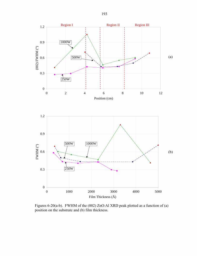
193
0
0.3
0.6
0.9
1.2
0 2 4 6 8 10 12
Position (cm)
(002
) FW
HM
(°)
1000W
250W
500W
Region I Region II Region III
(a)
0
0.3
0.6
0.9
1.2
0 1000 2000 3000 4000 5000
Film Thickness (Å)
FWH
M (
°)
1000W
250W
500W
(b)
Figures 6-20(a-b). FWHM of the (002) ZnO:Al XRD peak plotted as a function of (a)position on the substrate and (b) film thickness.

194
tail feature is included in the measurement. The FWHM decreases sharply to 0.43° at 5.7
cm in Region II, and steadily increases across Regions II and III to 0.69° at a position of
10.8 cm. The data marker at 10.8 cm is red indicating that the quantified peak is very
weak, and is therefore fit with an approximated Voight function to improve accuracy
mitigate signal to noise errors.
For 1000 W samples, the FWHM increases sharply across Region I from 0.416°
to 1.06° for the positions 0.8 and 4.2 cm, respectively, with 1.06° being the highest
FWHM measured for that sample. Both data markers for 1000 W samples in Region I
are red, indicating the tail feature is present in both. The FWHM at 4.2 cm is much larger
because the (002) peak is weaker, and therefore FWHM is measured across the tail
feature and it contributes significantly to FWHM. For the sample at 0.8 cm, the (002)
peak is of sufficient intensity that the tail does not contribute significantly to FWHM. In
a similar trend to 500 W data, 1000 W samples decrease sharply in FWHM between
Regions I and II, to 0.469° at 5.9 cm, followed by a steadily increasing with position to
0.607° at 9.3 cm.
For the FWHM of the (002) peak versus film thickness, there is a large degree of
variation in the data as a function of RF power for a film thickness greater than 2500 Å.
Thus no correlation between the FWHM and the film thickness is found in this region.
For films less than 2000 Å in thickness, which covers Regions II and III, the FWHM
shows much less scatter, and below 1500 Å, the FWHM steadily increases with
decreasing film thickness for all RF powers. Both the 250 W and 500 W data are
relatively constant between 2000 Å and 700 Å, before increasing sharply to the data
points for the thinnest films at ~300 Å. The 500 W trace in this region is offset slightly

195
higher in FWHM values. For 1000 W samples less than 2500 Å in thickness, 1000 W
FWHM increases nearly linearly with decreasing film thickness.
6.2.4 Atomic Force Microscopy Results
Tapping mode atomic force microscopy (AFM) was used to characterize the
surface morphology of the deposited thin films. Measurements are made on a roughly 7
x 7 mm square sample cleaved from the previously characterized XRD specimens.
Recall from Chapter 3 that the exact positions for the cleaved samples are not known,
therefore the data points are assumed to come from the sample’s center. Six samples are
measured for each RF power, totaling eighteen samples. A 0.5 x 0.5 µm area is measured
on each sample. Generally more than one measurement is made for each sample to
ensure that the micrographs are representative of the surface. Using stereological
techniques described in the experimental methods (section 3.4.3), sizes of the surface
morphological features in the micrograph are interpreted as “grain size”. As previously
discussed, the “grain size” is really the average size of distinctive granular surface
features. This method is illustrated in Figures 6-21(a-c), with the first figure (a) showing
a three-dimensional rendering of the sample’s surface with shades of gray conveying
height information. The second image (b) is a two-dimensional plot of the same
information. An analysis line corresponding to 400 nm on the image appears as a black
line from the 11 o’clock to 5 o’clock positions on Figure 6-20b. The output of the
analysis line is presented in Figure 6-21c as a profile of height information from under
the line, and is presented in the inset in the lower left corner of the AFM micrograph.
The “grain size” as a function of position and thickness is presented in Figures
6-22a and 6-22b, respectively. The “grain size” of the samples is larger for Region I
where the film is thickest, with maximum grain sizes of 440 Å, 800 Å, and 670 Å for the

196
(a)
(b) (c)
Figures 6-21(a-c). Process used to quantify “grain size” from AFM micrographs with (a)3-D rendering of the surface morphology, (b) plane view of the surface with the positionof a line scan showna line scan showing the topography of the surface in cross-section,and (c) cross section of the topography from the line scan.

197
250 W, 500 W, and 1000 W conditions, respectively. Grain sizes are smallest in Region
III, where the film thickness is thin, with minimum grain sizes of 230 Å, 310 Å, and 320
Å for the 250 W, 500 W, and 1000 W conditions, respectively. Even with the more than
an order of magnitude change in film thickness along the substrate’s length, grain size
varies by less than a factor four along the same length. Less variation was found with
position for each RF power condition, with variations of two times for 250 W and 1000
W conditions, and 2.5 times for 500 W.
For the 250 W sample, grain size fluctuates around a value of 400 Å ± 40 Å for
samples between the positions of 0.8 and 5.9 cm. The final two data points at positions
of 7.6 and 9.3 cm show a decrease in grain size to values close to 250 Å. For 500 W
samples, the first datum point at a position of 4.0 cm has the largest grain size, which is
800 Å. The value decreases significantly to 500 Å for the next datum point at 5.7 cm,
and then trends to smaller sizes with decreasing thickness, reaching a minimum of 310 Å
at 12.5 cm. For the 1000 W condition, grain size initially increases for the first three data
points from 590 to 680 Å for 0.8 to 4.2 cm. At 5.9 cm, in Region II, the grain size
decreases significantly to 450 Å, and continues to decrease in Region III to a value of 320
Å at 9.3 cm.
For the plot of “grain size” versus film thickness, there is a general trend to larger
grain sizes with increasing thickness independent of RF power. For films with a
thickness less than 1500 Å, the grain size trends to smaller grain sizes for thinner films
for the different powers. The traces for the different power conditions are offset, and
have different slopes, indicating more than film thickness is influencing “grain size” in
Regions II and III.

198
0
200
400
600
800
1000
0 2 4 6 8 10 12 14
Position (cm)
Gra
in S
ize
(Å)
1000 W
250 W
500 W
(a)
0
200
400
600
800
1000
0 1000 2000 3000 4000 5000 6000
Film Thickness (Å)
Gra
in S
ize
(Å)
500 W 1000 W
250 W
(b)
Figures 6-22(a-b). “Grain size” of the ZnO:Al thin films estimated from AFMmicrographs and plotted versus (a) position on the substrate and (b) film thickness.

199
The RMS roughness is plotted as a function of position and film thickness in
Figures 6-23a and 6-23b, respectively. The trends in RMS roughness versus position are
similar to those of grain size versus position. The RMS roughness varies by more than an
order of magnitude, with maximum values of 39 Å, 40 Å, and 70 Å for the 250 W, 500
W, and 1000 W conditions, respectively, all of which occur in Region I. The minimum
values occur in Region III, and are 5.8, 6.7, and 14.6 Å for the 250 W, 500 W, and 1000
W conditions, respectively. The RMS roughness measured for a bare glass substrate is
2.0 Å. The RMS roughness decreases monotonically with increasing position across
Regions II and III for all RF powers. Roughness for both 250 W and 1000 W samples
tend to be constant or increase slightly across Region I (positions less than 4.2 cm).
For the RMS roughness plotted versus the film thickness, no consistent trends for
the different power conditions are observed for films thicker than 2000 Å. Below 2000
Å, the RMS roughness monotonically decreases as the thickness decreases for all the
power conditions, but the lines are offset and the slopes are different. This indicates that
in general the RMS roughness decreases as the films become thinner, but that other
factors also influence the roughness in this thickness range.
6.3 Discussion of RF Power Experiment
6.3.1 Model of the Effects of Negative Ion Resputtering on Electrical Properties
Discussion of the results is facilitated by first presenting a model proposed to
explain them. In this model there are three separate regions at different positions on the
substrate. These regions are designated Region I, II, and III, and are equivalent to those
used to organize the results. The structure and properties are distinct for each of these
regions, and result from differences in the sputtered flux. Therefore, the discussion is

200
0
20
40
60
80
0 2 4 6 8 10 12 14
Position (cm)
RM
S R
ough
ness
(Å
)
1000 W
250 W 500 W
(a)
0
20
40
60
80
0 1000 2000 3000 4000 5000 6000
Film Thickness (Å)
RM
S R
ough
ness
(Å
)
500 W
1000 W
250 W(b)
Figures 6-23(a-b). RMS roughness of the ZnO:Al thin films measured by AFM as afunction of (a) position on the substrate and (b) film thickness.

201
organized by Region, with experimental results discussed in terms of the proposed model.
For these experiments, a position of 0 cm is directly below the source’s center, and
increasing values indicate increasing distance from this point. The substrate is also
positioned such that it is perpendicular to the uniformity shield, as shown in the cross-
sectional illustration of the proposed model in Figure 6-1. For 500 W samples, offset
data will be used during discussion to maintain this consistent reference to deposition
geometry.
Region I occupies areas with a direct vertical line of sight between source and
substrate, and is therefore exposed to the negative ion flux, and occurs consistently
between position 0 and 4.2 cm for this experiment. A direct vertical line of sight means
there are no obstructions between positions on substrate and target along a vertical path.
Negative ions are accelerated away from the target with a perpendicular trajectory
because the self bias electric field is perpendicular to the cathode. Negative ions are
reported to relax to neutrals during transport through the plasma, and therefore impinge
on the substrate as energetic neutrals [115]. Though they impinge on the substrate as
energetic neutrals, they will continue to be referred to as negative ions to distinguish their
source, and avoid confusion with other energetic neutrals that impinge on the target i.e.
reflected high energy Ar neutrals. The film’s structure and properties in this region are
strongly influenced by relationships between negative ion flux and deposited low energy
neutral flux [94,101,117].
Ion bombardment during thin film deposition was discussed in Section 2.4.3 of
the literature review. Again, though negative ions are neutralized before impinging on
the substrate, they will continue to be referred to as negative ions. Two important terms

202
describing ion bombardment are flux and energy. For negative ions, the flux is
equivalent to the negative ion current density (before the ions relax), and energy is kinetic
energy of the ion, which is controlled by the target self bias (voltage). Multiplication of
the target voltage and ion current density equals power density (Pd=V·J). The flux ratio
of negative ions to deposited neutrals is reported to critically control the magnitude of the
Negative Ion Resputtering effect [117]. Because this ratio is used extensively during the
discussion, it will be represented by the term J(ji/jn) with ji representing “negative ion”
and jn representing “deposited neutrals”, and J designates flux from the deposition source.
It is assumed for that increasing J(ji/jn) will result in increased damage due to ion
bombardment.
Changes in ion energy influence results of ion impingement in a complex way, as
is covered in the literature review. Ion-surface interactions include reflection, atom
displacement, implantation, and resputtering [101], with the magnitude of these processes
per incident ion being a function of the ion energy. Reflection of ions is not germane, as
this will not affect film properties. Resputtering will decrease deposition rates, and is
associated with atomic displacement in the film. Atom displacement at a surface can
improve or degrade film properties depending on the property and the energy of ions.
Low energy ions are utilized in Ion Beam Assisted Deposition (IBAD) and bias
sputtering to improve some film properties. IBAD involves using an ion source, typically
with He or Ar, focused on the substrate, and using the ion flux to improve film density or
optical properties. Bias sputtering typically involves negatively biasing the substrate
such that Ar ion in the plasma are attracted to the substrate [101]. Typically, ion energies
between ~10 and 100 eV can improve some film properties, while higher energies

203
typically degrade film properties. Higher ion energies are reported to result in subsurface
atomic displacement often generating Frenkel pair defects [101]. Implantation can also
influence the stoichiometry of the deposited material. For example implantation of
oxygen could change the stoichiometry of ZnO for areas exposed to oxygen ion
bombardment.
It is proposed that negative ion resputtering influences the electrical properties of
thin films by two mechanisms for compensation of conduction band carriers. One
mechanism is consumption of conduction band electrons by oxygen interstitials [78].
The oxygen interstitial is ionized by trapping a conduction band electron, which
maintains charge neutrality. Oxygen interstitials are generated by subsurface damage due
to negative oxygen ions impinging on the film. Oxygen interstitials can form by negative
oxygen ions being implanted and spontaneously coming to rest in an interstitialcy, or
Frenkel pair generation involving knocking oxygen from lattice site to an interstitialcy. It
is postulated that oxygen forms Frenkel pairs more commonly than zinc due to more
efficient binary collision energy transfer for oxygen because both atoms have the same
mass. Bonding in ZnO is between Zn and O, so to a first approximation interstitial
formation energy should be similar, but O is smaller, and is therefore anticipated to have
a smaller interstitial formation energy. This would help contribute to a higher
concentration of oxygen interstitials resulting from Frenkel pairs. It is postulated that the
resulting oxygen vacancy is often annihilated due to recombination with an oxygen atom
from the growth surface or implantation. It is important to consider if it is reasonable for
the large concentrations of oxygen interstitials needed to compensate degenerately doped
ZnO:Al to be present. The calculated size of the octahedral interstitialcy suggests that

204
oxygen can be accommodated. Additionally, one of the proposed models for native
defect doping for n-type ZnO transparent conductors is zinc interstitials. This supports
the case that large interstitial concentration can occur in ZnO. The larger size of the
oxygen ion (O-2=1.32 Å and O-1=1.76 Å) compared to the zinc ion (0.74 Å) suggests that
more tensile strain in the ZnO matrix might result from oxygen interstitials.
The second mechanism is compensation by deviations in stoichiometry.
Incorporation of excess oxygen is accommodated by formation of zinc vacancies. This
defect consumes two conduction band electrons normally supplied by an ionized zinc
atom to satisfy ionic bonding. The driving force for high oxygen incorporation into the
deposited film is the reactive character of energetic negative oxygen ions. Thus films
exposed to the negative ion flux grow in the presence of highly reactive energetic atomic
oxygen.
There is a transition between Regions I and II, which results from J(ji/jn)
decreasing and approaching zero across this area. This transition is consistently between
positions 4.2 and 5.7 cm on the substrate. Resistivities in this region are between those of
Region I and Region II, and improve as Region II is approached because J(ji/jn) is
decreasing.
Region II occupies areas not in direct vertical line of sight with the target, and
therefore receives no negative ion flux. Therefore one boundary is the uniformity shield,
which blocks the negative ion flux for areas below it. The boundary between Region II
and III occurs at higher position values, and is defined as where resistivity increases
roughly by a factor of two over the Region II resistivity. Region II is not exposed to
negative ions due to shadowing, but does receive a neutral flux because of the power
205
cosine distribution for the angular dependence of material ejected from the target [101].
Film properties in this region are independent of RF power, but are influenced by the
more traditional process parameters of pressure and substrate temperature. The film
properties in Region II are the best achievable with the process conditions used because
degradation by negative ion bombardment does not occur. The width of Region II
depends on deposition conditions including RF power and deposition time, because
Region III is defined in terms of thickness. It occurs for areas where the film thickness is
less than 500 Å and that receive no negative ion flux. For example, if film thickness is
less than 500 Å for all the areas shadowed from negative ion resputtering, in which case
there is no Region II at all.
In Region III, thickness dominates the electrical properties. Deposition of films in
Region II and III depend on flux which is not parallel to the targets normal, i.e. flux
resulting from a power cosine distribution of ejected material from a sputtering target.
The power cosine distribution specifies that flux decreases as the angle relative to the
target’s normal direction increases [94,99]. Thus, the flux that reaches the substrate is the
integrated amount of flux received from all unobstructed points on the target. At larger
positions on the substrate, the uniformity shield increasingly obstructs the target,
decreasing the flux. At some position, the integrated flux is too low and the film is so
thin that it dominates the film’s resistivity.
There are three possible mechanisms for increased resistivity with decreasing film
thickness in Region III. The agreement between these mechanisms and the data will be
discussed in sections 6.3.4.2 to 6.3.4.4 below, which are concerned with the resistivity,
carrier concentration, and Hall mobility in Region III. Chemisorption of oxygen species
206
is proposed to be the dominant mechanism for increased ZnO:Al thin film resistivity with
decreasing film thickness. Chemisorbed oxygen species on the free surface and grain
boundaries are known to reduced carrier concentration in ZnO film solid state gas sensors
[9], and are therefore proposed to cause the decreasing carrier concentration, which is the
dominant source of the increased resistivity in Region III. This mechanism was
previously proposed to explain the decreasing carrier concentration with decreasing film
thickness found in data presented in section 5.3.2. Another possible mechanism for the
increased resistivity is based on the Fuchs and Sondheimer model, which applies to very
thin metallic films [133,134]. The Fuchs and Sondheimer model was also presented in
Chapter 5, and postulates that as thickness decreases, interfacial scattering may reduce
the electron carrier’s mean free path, which reduces carrier mobility and increases
resistivity. A decrease in Hall mobility is observed (Figure 6-10), but only by a factor of
~2. Instead, the carrier concentration is strongly reduced by up to an order of magnitude
in Region III compared to Region II, which suggest interface scattering is not the
dominant mechanism for increasing resistivity. A third mechanism to explain Region III
resistivity data is an increased concentration of interface states, which is predominantly a
function of grain size until film thickness approaches the grain size. Interfaces states act
as electron carrier traps, and therefore decrease carrier concentration [87]. When this
occurs, grain size in the vertical dimension will be constrained by film thickness. As the
film becomes thinner, vertical grain size will decrease, and the free concentration of
interface states will increase, decreasing the carrier concentration.
Turning attention to the RF power used to deposit the films, this varied parameter
is important in this model by its influence on the magnitude of the negative ion

207
resputtering. Its primary influence is on the self bias of the target, which increases with
RF power. A higher target potential will increase the energy of negative ions, which
affects negative ion resputtering in ways previously discussed. The factor J(ji/jn), which
cannot be measured or derived easily, is assumed to depend only weakly on the RF power
used to deposit the film.
6.3.2 Region I
In Region I, the model predicts that substrate is in direct line of sight with the
target, and therefore receives a strong negative ion and deposited neutral flux.
Investigation of negative ion resputtering involves comparing differences between areas
which are and are not resputtered, and differences between positions where J(ji/jn)
changes. Comparison between Regions I and II corresponds to the negative ion flux
versus no negative ion flux comparison. Comparisons within Region I and for the
transition between Regions I and II correspond to comparisons for changing negative ion
flux, which affects the flux ratio of negative ions to deposited neutrals (J(ji/jn)).
6.3.2.1 Profilometry (Region I)
Deposition rate (Figure 6-3), and therefore film thickness (Figure 6-2) versus
position on the substrate are predicted to depend on the target edge effects, and amount of
negative ion resputtering, and RF power used to deposit the film for Region I. The
deposition rate decreases between positions 0.6 and 4.2 cm by 30% and 35% for 250 W
and 1000 W data, respectively. The smoothly decreasing deposition rate is consistent
with target edge effects, or the decreasing deposition rate as the edge of the RF diode
sputtering source is approached [117], with the target’s edge effectively defined by the
uniformity shield. Negligible sputtered flux is generated for areas of the target under the

208
electrically grounded uniformity shield, as the shield interrupts the plasma in this region,
and obstructs the negative ion flux from reaching the substrate.
The relative effect of negative ion resputtering versus the sputter deposition rate
depends on J(ji/jn). To investigate the influence of negative ion resputtering on
deposition rate, comparisons between areas that do and do not receive negative ion flux
must be made. Deposition rate decreases smoothly with increasing position across
Regions I and II for all RF powers. This suggests that growth rate in Region I is not
dominated by negative ion resputtering effects. As discussed in Chapter 2, a strong
negative ion resputtering effect can result in dramatically decreased growth rates, and
possible even etching of the substrate.
The ratio of the deposition rate between 250 W and 1000 W samples, and 500 W
and 1000 W samples as a function of position is presented in Figure 6-5. For 250 W data,
the ratio is consistently near 22% in Region I, which agrees with the ratio of RF powers
(25%) between the two conditions. For 500 W data, the two data point in Region I are
consistently 57%, which is a small degree above the ratio of RF powers between the two
conditions (50%). The 500 W/1000 W ratio data is expected to have poor accuracy
resulting from two sources of error, the first of which is small inaccuracies in the
positional offset applied to the 500 W data. A small inaccuracy in position offset can
have a significant effect on the relative deposition rate data because of steep slopes of the
deposition rate data versus position. The second source of error also results from the
offset position, and results from misalignment of the positions for data points. Therefore
linear interpolation between the data points was required to get 500 W and 1000 W
deposition rate data for the same positions. These sources of error occur for all Regions.

209
The molecular deposited flux was calculated from deposition rate data and plotted
in Figure 6-4. The molecular flux decreases with increasing position, with a trend similar
to half of a bell-curve. Values of the molecular flux are taken to be approximately equal
to the deposited neutral flux (jn). The ratio of the negative ion to deposited neutral flux is
an important factor in controlling the magnitude of the NIR effect on materials properties,
and it is therefore useful to estimate the negative ion flux. The estimation is based on
changes in the carrier concentration because it is will be shown below to be sensitive to
NIR. In Region I, the carrier concentration is decreased by as much as 90% compared to
Region II. If the entire decrease in carrier concentration is attributed to NIR, and it is
assumed that one negative ion generates an average of one compensating state, then the
negative ion flux must be such that it can generate ~5x1020 cm-3. The negative ion flux
calculated based on ~5x1020 cm-3 compensating states indicates that J(ji/jn) is
approximately 0.01 or 1%. The low negative ion flux is consistent with the lack of sharp
changes in deposition rate between Region I and II, as a large negative ion flux causes
decreased deposition rates for areas subjected to NIR. The value of one compensating
state per incident negative oxygen ion is reasonable considering the sputter yields for
oxygen are typically on the order of one atom sputtered per incident oxygen. For higher
negative ion kinetic energies, some ions will be implanted. The impinging ion can
generate compensating states through an initiation of a collision cascade in the deposited
film, when the ion comes to rest on an interstitial site, and when a zinc vacancy is
generated. It is therefore reasonable that each implanted ion generates on average of one
compensating state.
210
6.3.2.2 Resistivity effects (Region I)
For 250 W samples in Region I, curvature is found with resistivities ranges from
3.3x10⁻³ to 7.0x10⁻³ Ω·cm between 0.6 and 4.5 cm, respectively, as seen in Figure 6-7.
Thus, the resistivity is slowly increasing with distance from the source’s center. The
increase in resistivity results from an increase in negative ion resputtering. More
resputtering results from a larger J(ji/jn) as positions approach the uniformity shield’s
edge (which effectively defines the edge of the deposition source). For higher positions
in Region I, J(ji/jn) decreases, i.e. the flux of deposited material decreases as the edge of
the target is approached, while the negative ion flux remains constant for all areas
exposed by a direct line of sight to RF diode source. Negative ion flux remains constant
because it has a narrow distribution of departure angles centered on the targets normal
axis. The changes in flux rates with position are schematically illustrated in Figure 6-1.
Resistivities of 250 W samples are always lower than 1000 W samples in this region, and
from the plot of resistivity versus film thickness in Figure 6-8, there is no correlation
between resistivity for different RF powers with film thickness. More RF power
correlates with increased resistivity. XRD evidence discussed below suggests increasing
resistivity with RF power results from differences in the target’s negative bias which
increases from –300 V to –1000 V with increasing RF power from 250 W to 1000 W,
respectively. Negative ion energy increases with target bias, while the generation rate of
negative ions per Ar+ incident on the target is not expected to change significantly across
this range of target potentials. Lower negative ion kinetic energy will result in less
resputtering and damage for the film. Thus, lower resistivities for 250 W versus 1000 W
samples is consistent with a decrease in negative ion kinetic energy.

211
For 1000 W samples, resistivity is consistently 1.25x10⁻² Ω·cm for positions
between 0.6 and 4.5 cm, as seen in Figure 6-7. The value of J(ji/jn) is expected to vary
with position in the same manner as 250 W samples. The lack of variation is attributed to
a saturation of the effects of damage on resistivity, whereby increasing J(ji/jn) has little
influence on resistivity. A possible mechanism for higher RF powers is that the target
bias is increased, yielding a larger fraction of implanted oxygen and more Frenkel pairs
of oxygen on a lattice and interstitial sites due to ion bombardment. This effectively
drives stoichiometry to oxygen rich. The sticking coefficient for normal oxygen
decreases with excess oxygen, which moderates film composition. In turn film
composition is critically important to doping due to intrinsic doping and compensation
mechanisms.
For 500 W samples, there are only two data points in Region I. Resistivities at
these points were 2.5x10⁻² and 1.1x10⁻² Ω·cm for 3.8 and 4.5 cm, respectively, with the
former being a small degree higher than 1000 W samples. Again, changes in resistivity
with RF power are attributed to variation in negative ion energy due to target self bias.
Negative ion energy is not expected to influence electrical properties linearly because the
energy influences relative quantities of all four primary ion-surface interactions. It is
speculated that for 500 W, which has a target bias of ~500 V will result in less
implantation of O, but more damage to the growth surface.
The sharp decrease in resistivity for the transition between Regions I and II occurs
at the same position for all three RF powers, with the decrease occurring between 4.2 and
5.7 cm. Some variation in slope occurs due to differences in resistivity on the Region I
side. This strong drop in resistivity to the Region II minima of 1.5x10⁻³ Ω·cm results

212
from a large decrease in J(ji/jn). Both fluxes are decreasing due to shadowing from the
uniformity shield, but narrow angular distribution for negative ions causes this flux to
decrease more rapidly than the deposited neutral flux. This region is roughly 1.2 cm in
width, and is at a distance of 9 cm from the target, suggesting the negative ion flux has an
angular distribution confined to less than 10° off perpendicular.
6.3.2.3 Hall carrier concentration (Region I)
For all three Regions, Hall data are presented with 0.8 cm errors bars to indicate
the uncertainty of the position where the samples are cleaved. To help mitigate this
positional uncertainty, Hall resistivity is brought into agreement with four point
resistivity by adjusting the film thickness and position. Four point probe and
profilometry data are taken within 1 mm of the marked positions, and therefore have high
positional accuracy. Resistivities derived by the Hall systems software depends on the
film thickness entered into the software. If the actual film is thicker than the value
entered, then the actual resistivity is higher and carrier concentration is lower than the
values derived by the computer, and visa versa if the actual film thickness is thinner than
the entered value. Calculation of Hall mobility derived by the van der Pauw method
[121] does not depend on the film thickness, and therefore adjusting the film thickness
does not influence Hall mobility. Film thickness is a function of position, and therefore
as the film thickness for the Hall sample is adjusted, the position of the sample must be
adjusted to maintain consistency with the thickness to position relationship. The
thickness adjustments made are within the range of thicknesses defined by the positional
uncertainty. This procedure is only done for samples with more than a 20% deviation
between the Hall and four point probe resistivities. The improved relationship between
Hall and four point probe resistivity can be appreciated in the plot shown in Figure 6-24.

213
This is a plot of resistivity as a function of position, and shows that good correlation can
be achieved by adjusting the film thickness and position within their known boundaries.
Data points that have changed are shown in orange. Corrected carrier concentrations are
plotted as a function of both position and thickness in Figures 6-25a and 6-25b. The
discussion of Hall data will be based on plots from corrected data.
In Region I all samples have lower carrier concentrations than in Region II. The
carrier concentration for 250 W samples varies in Region I, and the variations are
consistent with the previously described changes in resistivity. Resistivity increases and
carrier concentration decreases by factors of 2.1 and 1.9 for 250 W samples across
Region I, respectively. This indicates carrier concentration is responsible for most if not
all of the changes in resistivity. Variations in carrier concentration are postulated to
0.001
0.01
0.1
1
10
0 2 4 6 8 10 12 14
Position (cm)
Res
istiv
ity (
Ω·c
m)
500W
250W
1000W
4 Pt. ProbeHall
Region I Region II Region III
Figure 6-24. Resistivity of the ZnO:Al thin film with the Hall resistivity (dashed)corrected to agree with the four point probe resistivity (solid) versus position.

214
0.00E+00
2.00E+20
4.00E+20
6.00E+20
8.00E+20
0 2 4 6 8 10 12 14
Position (cm)
Car
rier
Con
cent
ratio
n (c
m-3)
1000W
500W
250W
Target Doping Level
Region I Region II Region III
(a)
0.0E+00
2.0E+20
4.0E+20
6.0E+20
8.0E+20
0 1000 2000 3000 4000 5000 6000
Film Thickness (Å)
Car
rier
Con
cent
ratio
n (c
m-3)
1000W
500W250W
Target Doping Level
(b)
Figures 6-25(a-b). Corrected carrier concentration from Hall measurements for ZnO:Althin films as a function of (a) position on the substrate and (b) film thickness.
215
result from changes in J(ji/jn) as a function of position, with variations in J(ji/jn) resulting
from the same mechanisms presented during discussion of resistivity for this sample
(Figure 6-1). Without changes in mobility, it is clear that negative ion resputtering
influences resistivity by changes in carrier concentration. This is consistent with the
postulate in the model that negative ion resputtering causes compensation of electron
carriers by increasing interstitial oxygen concentration and/or higher than stoichiometric
oxygen incorporation resulting in zinc vacancies.
There is only one 500 W datum point in Region I for carrier concentration, which
is at 4.0 cm with a value of 7.5x1019 cm-3. Note that from quantified XRD data, this point
is labeled with a red marker to indicate a significant tail to higher 2θ values for the (002)
peak. The 500 W sample is ~2.4 times lower in carrier concentration than the 250 W
sample for the same position, while the 500 W sample is ~1.8 times higher in resistivity
than the 250 W sample. This is consistent with decreased carrier concentration by
increased damage from negative ion resputtering. Data from SIMS measurements
discussed below indicates that the changes in carrier concentration do not result from
changes in the Al dopant concentration or compensation by alkali metals, which is
consistent with the proposed native defect mechanisms.
For 1000 W samples, red markers are also used in XRD data for the two positions
(0.8 and 4.2 cm) from Region I. As a reminder, no data were collected for the position of
2.5 cm because the sample was inadvertently broken before XRD could be collected.
Carrier concentrations for these positions have very low carrier concentrations with
values of 7.1x10¹⁹, 7.3x10¹⁹, and 1.5x1020 cm-3 for positions 0.8, 2.5, and 4.6 cm,
respectively. Increased carrier concentration for position 4.6 cm suggests this sample is

216
in the transition between Regions I and II, and therefore is partially shadowed from
negative ions, which decreases J(ji/jn). Lack of variation in carrier concentration is
consistent with the lack of variation in resistivity found for 1000 W samples in Region I.
Thus, for 500 W and 1000 W samples, Region I has low carrier concentration
consistently near 7.4x1019 cm-3. The constant low carrier concentrations and lack of
variation in electrical properties for 1000 W samples in Region I despite expected
changes in J(ji/jn) versus power or position are consistent with saturation. The saturation
effect was postulated to explain the constant resistivities in Region I for 1000 W samples.
The sources and implications of the XRD tail and its relationship to low carrier
concentrations will be discussed further below.
For the transition between Regions I and II, resistivity decreases sharply from 4.2
and 5.7 cm for all three RF powers, and correlates well with a strong increase in carrier
concentration. Between Region I and II, resistivities decrease by factors of 2.9, 6.0, and
7.6 for 250 W, 500 W, and 1000 W samples, respectively. Carrier concentrations
increase by factors of 2.8, 4.5, and 7.3, respectively, indicating changes in carrier
concentration are responsible for approximately 100%, 75%, and 95% of decrease in
resistivity between Regions I and II. These data are consistent with the postulated
relationship between negative ion resputtering and carrier concentration.
6.3.2.4 Hall mobility (Region I)
Corrected Hall mobility data are replotted in Figures 6-26(a-b) as functions of
position and thickness, respectively. As previously described, it is the position and
thickness that changes with the correction, not Hall mobility values. Within each RF
power for Region I little variation in Hall mobility is found, which is consistent with
small variations in resistivity and carrier concentration. Hall mobility for 250 W samples

217
0
5
10
15
0 2 4 6 8 10 12 14
Position (cm)
Hal
l Mob
ility
(cm
2/V·s
)500W
250W
1000W
Region I Region II Region III
(a)
0
5
10
15
0 1000 2000 3000 4000 5000 6000
Film Thickness (Å)
Hal
l Mob
ility
(cm
2/V·s
)
1000W
500W
250W
(b)
Figures 6-26(a-b). Corrected Hall mobility for ZnO:Al thin films as a function of (a)position on the substrate and (b) film thickness.

218
is within ±1 cm2/V·s of the average value 7.1 cm2/V·s, which is less than experimental
error. For 1000 W samples, the average Hall mobility is Region I is 7 cm2/V·s, and there
is no significant variations outside of experimental error. For samples deposited at 500
W there only datum point from Region I (with a position of 4.4 cm) and has a mobility of
11 cm2/V·s, which is substantially higher than for 250 W and 1000 W samples. Low
carrier concentration for this sample suggests that it is more compensated by oxygen
interstitials and/or zinc vacancies than the 250 W sample. The higher concentration of
point defects in the 500 W sample should decrease carrier concentration if point defects
are dominating carrier mobility. This suggests there is another unknown parameter
influencing mobility.
There is not sufficient data from the transition between Regions I and II to
evaluate trends in Hall mobility. For 250 W and 500 W data, no changes outside
experimental error occur between 4 cm (Region I) and 6 cm (Region II). For 1000 W
samples, the mobility increase by a factor of 1.4 from Region I to II, but this is small
compared to the change in resistivity and carrier concentration. In terms of the model,
carrier concentration and resistivity have changed significantly between Regions I and II
due to changes in negative ion flux reaching the substrate, while little or no change
occurs in Hall mobility. This supports the postulate that negative ion resputtering
primarily affects carrier concentration. The lack of influence from the proposed changes
in point defect concentrations between Regions I and II on the mobility suggests another
scattering mechanism is dominating the mobility.
Ionized impurity scattering is often reported in the literature as the dominant
scattering mechanism in degenerately doped ZnO:Al thin films [60,89], but other reports

219
refute this claim [96]. In this study, large changes in carrier concentration occur between
Regions I and II, with no correlation to changes in mobility. This suggests that ionized
impurity scattering is not the dominant scattering mechanism limiting mobility. As
reported above and discussed below, XRD and AFM data varies significantly across
Region I and II, yet Hall mobility shows little change. This suggests that some factors
not being detected or measured precisely by XRD or AFM are influencing the mobility.
Point defects and line defects are not detected by these structural characterization
techniques, but can affect scattering. Because point defects are known to be very
important to electrical properties [85,89,139], it seems likely that they are controlling the
mobility. Also, as will be shown below, carrier mean free path is calculated to be ~5 Å, a
dimension similar to unit cell size. The calculated carrier mean free path seems
unrealistically short, but is in agreement with reported values [82]. Point defects or a
combination of point defects and other defect scattering mechanisms are only scattering
mechanisms that might be possible in the concentrations indicated by the small carrier
mean free path.
6.3.2.5 Secondary ion mass spectrometry
The SIMS data are used to evaluate changes in Al and Na concentrations in the
film. Aluminum is the extrinsic dopant, and alkali metals can compensate electron
carriers, therefore changes in the concentrations of these elements are potentially
responsible for the changes in carrier concentration that are found between Regions I and
II. From the plots of the Al to Zn ratio, it is clear that the concentration of Al does not
change for the 250 W case, and is slightly higher in Region I compared to Region II for
the 500 W and 1000 W cases. This suggests that there is actually a small increase in the
dopant concentration in Region I, which is where the carrier concentration is drastically

220
lower relative to Region II. Thus, the changes in Al dopant concentration do not agree
with changes in the carrier concentration, which suggests that decreased Al concentration
is not responsible for lower carrier concentration in Region I.
The ratio of Na to Zn makes only small changes between Regions I and II, with a
slightly lower ratio of Na in Region I being typical. This reveals that the concentration of
Na is lower in Region I compared to Region II. Because Na acts to compensate electron
carriers, the trend in Na concentration is opposite of what would cause lower carrier
concentrations in Region I compared to Region II. Additionally, the Na to Zn ratio was
found to be at most one order of magnitude larger than the Al to Zn ratio. Recall that the
sensitivity of SIMS to Na is anticipated to be several orders of magnitude larger than for
Al, which suggests that the Na concentration is not large enough to cause the up to 90%
lower carrier concentration in Region I compared to Region II.
The SIMS data indicates that the two most likely extrinsic sources for decreased
carrier concentration, which include loss of the Al dopant due to preferential resputtering
and incorporation of Na from the soda-lime glass substrate, are not occurring in the
deposited films. The lack of extrinsic causes for the change in carrier concentration
suggests that a intrinsic mechanism involving native defects is responsible. This is
consistent with the mechanism for compensation proposed in the model which involves
formation of oxygen interstitials and/or zinc vacancies due to bombardment by negative
ions.
6.3.2.6 X-ray photoelectron spectroscopy
Data from XPS measurements are used to evaluate to composition and atomic
bonding for the surface of the deposited ZnO:Al thin films. Only Zn, O, and C
characteristic peaks are found for the as deposited state suggesting that carbon is the only

221
contaminant. A carbon peak is no longer detected after sputter etching for 6 minutes,
indicating that carbon is a surface contaminant, which is consistent with adventitious
carbon from the atmosphere.
Atomic concentrations of elements at the surface and shifts in peak energy
associated with chemical bonding are evaluated using higher resolution multiplex data.
The qualitative atomic concentration data presented in Table 6-1 indicate that the as
deposited film’s surface is 34% C, 53% O, and only 13% Zn. The much higher
concentration of O compared to Zn indicates oxygen is present on the surface
significantly in excess stoichiometry. After sputter etching for 6 minutes, the
concentration of Zn has increased to 45%, while the oxygen and carbon concentrations
decreased to 48% and 7%, respectively. The Zn and O concentrations are within
experimental error of being stoichiometric, which indicates that the excess oxygen is also
a surface feature.
A significant change in peak shape and area occur between as deposited and
sputter etched spectra. A well-defined double peak is observed in the oxygen multiplex
data (Figure 6-14a), with a higher binding energy (532.2 eV) and a lower binding energy
(530.7 eV) peak. The high and low energy peaks account for 67% and 33% of the peak
area, respectively. After sputter etching for six minutes, the areas of the high and low
energy peaks change markedly, and comprise 7% and 93% of the peak area, respectively.
The [140] and reports in the literature suggest that the chemically shifted higher energy
(532.2 eV) peak is consistent with a surface oxide species. The chemical shift cannot
explicitly identify if the surface species is oxygen, hydroxide, or a combination of both.
These results are consistent with chemisorbed oxygen, and therefore offer physical

222
evidence which supports the hypothesis that chemisorbed oxygen is the source for
compensation of electron carriers for the less than 500 Å films in Region III.
6.3.2.7 X-ray diffraction (Region I)
Quantification of XRD results focused on peak intensity (counts), 2θ peak
position (degrees), and full width half maximum (FWHM) (degrees). Diffracted intensity
is a function of the fraction of sampled volume that satisfies the Bragg condition for a
given 2θ angle. All films are thinner than the X-ray beam’s sampling depth (~5 µm),
therefore intensity is expected to be a function film thickness, with thinner films yielding
less intensity at the peak maximum if all else is equal [110]. The 2θ peak positions
depend on lattice d-spacings between crystal planes. This is not expected to be a function
of thickness, but is sensitive to shifts in d-spacing resulting from out-of-plane strain
[110]. The FWHM characterizes the diffracted peak’s breadth. The breadth is influenced
by instrument broadening, which is assumed to be constant. Breadth can also be
increased by variations in d-spacings, and changes in domain size over which coherent
scattering occurs. Larger domain or crystallite sizes result in larger volumes of coherent
scattering, which results in a smaller FWHM. As domain size decreases, FWHM
increases. Thus, because the vertical domain size in very thin films becomes dependent
on the film thickness, the FWHM is expected to increase as the film thickness decreases.
Thus, both film thickness and crystal quality must be considered during interpretation of
XRD [110].
All data are quantified from the (002) or basal plane 2θ peak of wurtzite phase of
ZnO. Line profile spectra are used for quantification of 250 W and 1000 W data, and
survey spectra are used for quantification of 500 W data, as discussed in Chapter 3. The

223
(002) peak is consistently the most intense, which indicates the film has a strong basal
plane texture. This suggests that adatoms have sufficient surface mobility that they can
migrate over large distances to facilitate growth of low free energy (002) crystal planes.
This occurs despite water cooling of the substrate support and changes in impingement
angle, negative ion flux, and deposited neutral flux. The JCPDS database indicates the
(002) peak occurs at 34.422° 2θ for pure ZnO and Cu Kα X-rays. Discussion of XRD
data will be broken down into sections based on data type, and will cover variations in
intensity, 2θ peak position, and FWHM, so that positional effects and film thickness
effects can be evaluated together.
Maximum peak intensity data are plotted as functions of position and film
thickness in Figures 6-18a and 6-18b, respectively. Intensities from 500 W samples are
consistently lower because shorter count times are used in the XRD survey spectra. Both
250 W and 1000 W samples show a monotonic decrease in intensity across Region I.
The fact that intensity increases in Region II despite thinner films, suggests that
decreasing film thickness accounts for only part of the decreased intensity in Region I.
The proposed model postulates that J(ji/jn) increases with position across Region I due to
target edge effects and the narrow angular distribution of negative ions leaving the target.
It is postulated that as J(ji/jn) increases, structural damage to the film is also increasing.
Structural damage would act to reduce domain size, which would broaden the peak. A
broader peak will have a lower peak intensity. This suggests that increased FWHM and
decreased film thickness across this region are both responsible for decreased peak
intensity in 250 W and 1000 W samples across Region I. This is supported by increases
in FWHM with increasing position across Region I for 250 W and 1000 W data.

224
Before 2θ peak positions are discussed, recall that red data markers are used in
quantified XRD results to signify a highly anisotropic peak shape. The anisotropy is best
appreciated by examining those spectra presented in Figures 6-16b and 6-17b. Also note
that red data markers in Region I are associated with 2θ peak positions that are roughly
0.2° lower than Region II values. Four points marked in red include 1000 W samples
from 0.8 and 4.2 cm, and 500 W samples from 4.0 and 10.8 cm. The three data points
from Region I are marked due to a significant tail on the peak, which extends to larger 2θ
values. The 500 W sample at 10.8 cm is marked because the peak in very weak and
therefore might have significant error due to noise. Also notice that no red markers are
used for 250 W data. This fact suggests that the tail feature is a function of deposition
power. Red data markers in Region I are also associated with positions where carrier
concentrations are significantly lower and resistivities are significantly higher than
Region II.
All 500 W and 1000 W data points have red data markers, indicating the presence
of the tail to higher 2θ values for the basal peak. Presence of the tail is also associated
with a large (0.2°) increase in 2θ position between Regions I and II. If spectra for these
points are examined, the tail is found to extend roughly 2° higher in 2θ than the peak.
Significant diffraction for 2θ values larger than the JCPDS value indicates both
contraction and expansion of the c-axis occur in the surface normal direction. The out-
of-plane expansion is attributed to high interstitial concentrations, and is discussed in the
following paragraph. One possible mechanism for out-of-plane lattice contraction is
mismatch between the thermal expansion coefficients of the glass substrate and the ZnO
film. The coefficients of thermal expansion (α with units of K-1) are 8.8x10⁻⁶, 4.75x10⁻⁶,

225
and 2.92x10⁻⁶ K-1 for soda lime float glass, a-axis ZnO, and c-axis ZnO, respectively.
Thus, for a film and substrate cooling after unintentional heating during deposition, the
substrate will contract more than the film, yielding in-plane compressive strain. To
maintain constant unit cell volume, out-of-plane lattice expansion may occur [101].
Thus, strain induced due to the mismatch of thermal expansion coefficients is not
consistent with out-of-plane contraction. Ion peening can generate compressive strain in
the out-of-plane axis. This process involves film bombardment by energetic particles,
which cause deformation of chemical bonds to force atoms closer together. At low
growth temperatures the deformation does not relax, freezing damage into the lattice.
The tails has significant intensity only for 500 W and 1000 W samples where the 2θ peak
position is shifted to significantly lower values. At these powers, negative oxygen ions
have approximately 500 eV and 1000 eV kinetic energy, respectively. This suggests that
ion peening is intensified by higher ion kinetic energies.
Another possible contribution to out-of-plane compressive strain is a non-uniform
distribution of interstitials within the ZnO grains. If grain boundaries act to deplete
interstitials by a gettering and desorption mechanism, then constant grain volume could
be maintained by expansion in the grain’s center to accommodate interstitials in balance
with contraction in outer portions of the grain where interstitial concentrations are
depleted. Gettering is postulated to increase at higher temperatures, and higher substrate
temperatures are expected with higher deposition powers [94,99,101]. Also, interstitial
concentrations are postulated to increase with increasing ion energies. Both of these
effects would yield increased out-of-plane expansion and contraction for higher ion
energies. Because it seems plausible that collision cascades from negative ions would

226
subsequently disturb strain induced by ion peening, the postulate of non-uniform
interstitial concentrations is considered more likely.
The 2θ peak position for 250 W samples has significantly less variation than 500
W and 1000 W samples. The peak position for 1000 W samples in Region I is more than
0.5° lower in 2θ than the value for pure ZnO, which translates to a 1.6% larger d-spacing
in the out-of-plane direction (i.e. the [0001] direction). In terms of residual stress, the
film has tensile out-of-plane stress. For sputtering, this typically results from lattice
expansion due to a high concentration of interstitials [101]. These interstitials are either
implanted Ar atoms reflected from the source, or Frenkel pairs from impingement of the
high energy reflected Ar atoms. In-plane expansion is constrained by bonding to the
substrate, and therefore results in bi-axial in-plane compressive stress [94,101]. If this
stress is sufficiently large, film delamination can result. The out-of-plane dimension is
not constrained, and therefore expands to accommodate the high interstitial
concentration. Because the 2θ peak position moves towards the pure ZnO value in
Region II, the increased interstitial concentration suggested by out-of-plane lattice
expansion is postulated to result from negative oxygen ions. The negative ions impinge
on the film, in which some are implanted and come to rest in interstitial positions. Other
negative ions form Frenkel pairs during the collision cascade within the film. As
mentioned in the model first postulated in Section 6.3.1, Frenkel pairs with oxygen as the
interstitial should be more common due to efficient binary collision energy transfer with
other oxygen atoms. The 500 W sample at 4 cm also has a significantly lower 2θ peak
position than the pure peak, suggesting it also has a high concentration of interstitial
oxygen. The 500 W and 1000 W samples are both shifted ~0.2° lower in 2θ in Region I,

227
compared to Region II. For 250 W samples, the peak position is 0.09° lower in Region I
than Region II. If Regions II and III are considered to have minimal interstitial
concentrations, then the smaller change in 2θ peak position 250 W is consistent with
higher carrier concentration due to less compensation by oxygen interstitials, which was
found in Hall data. There are both octahedral and tetrahedral interstitial sites available in
ZnO. Comparing the equilibrium size of the interstitial site to the size of single and
doubly ionized oxygen ions, the oxygen ions are 4% and 38% larger than the tetrahedral
site for single ionized and double ionized oxygen, respectively. For an octahedral site,
the oxygen ion is 30% and 6.4% smaller for the singly and doubly ionized oxygen,
respectively. Because the interstitial sites are bounded by oxygen ions in the ZnO lattice,
strong repulsive coulombic forces are anticipated between the interstitial and the lattice.
This suggests that oxygen ions smaller than the interstitial sites can cause tensile strain in
crystals that are free to expand. Both the singly and doubly ionized oxygen ions are
larger than the tetrahedral sites, which indicates that this configuration would generate a
large amount of strain, and is therefore likely to be energetically unfavorable. The offset
to lower 2θ peak positions for Regions II and III will be discussed subsequently.
For the transition between Regions I and II, the 2θ peak positions for all RF
powers move to higher values, which are closer to the JCPDS value for basal plane
diffraction. The high 2θ tail is not observed for the (002) peak. Low negative ion
resputtering in Region II is supported by the correlation between electrical properties and
position. The changes in peak position and loss of the high 2θ tail correlate well with the
decrease in resistivity between Regions I and II.

228
For FWHM, 250 W and 1000 W data was quantified by the Line Profile Analysis
[122] software from Philips, and 500 W data was quantified using the MacDiff [128]
software package using procedures reported in Chapter 3. In Region I, large variations
are found for the 1000 W data. The large increase in FWHM for samples from positions
0.8 and 4.2 cm results from the previously mentioned tail. The well-defined basal peak is
sufficiently intense from the 0.8 cm sample that the tail is below half the maximum
intensity, and therefore contribute little to the FWHM. At 4.2 cm, the basal peak and tail
intensities are similar, therefore the tail contributes to a much larger FWHM at this
position. This is similar to 500 W data at 4.0 cm, whose large breadth also includes a
significant contribution from the tail. Again, the tail is postulated to result from a
combination of a non-uniform distribution of oxygen interstitials and ion peening.
For 250 W data, no significant tail can be detected for any sample in Region I.
Thus, the tail is only associated with higher target biases from higher RF powers. The
FWHM does increase across Region I for 250 W samples. The increase in FWHM is
consistent with thinner films, but the subsequent decrease in FWHM with thinner films
between Regions I and II suggests another factor besides film thickness is influencing
FWHM. Changes in FWHM for 250 W data are postulated to result from a combination
of decreasing film thickness and degraded crystallinity in the films. Changes in peak
position are small (0.06°), which suggests change in strain is small. This suggests that
little of the broadening in 250 W FWHM data results from changed peak asymmetry
induced by strain. For 500 W and 1000 W samples, peak asymmetry cannot be evaluated
due to the presence of the tail. Increased FWHM associated with higher positions (i.e. ~4

229
cm) in Region I is consistent with degraded crystallinity caused by an increase in J(ji/jn)
with higher positions.
6.3.2.8 Atomic force microscopy (Region I)
Analysis of atomic force microscopy (AFM) images is used to quantify “grain
size” and surface roughness. Recall that the technique used to quantify grain size is
based on interpretation of granular surface features as distinct grains of the
polycrystalline thin film. No variation in grain size outside of experimental error is found
for 250 W and 1000 W samples in Region I. At 4 cm, grain size from highest to lowest
occur for 500 W, 1000 W, and 250 W samples, which correlates with film thickness.
Thus, differences in grain size correlate with film thickness, with larger grain sizes
associated with thicker films. Thus thickness influences grain size, but the lack of
consistent correlation suggests other factors are also involved. For 500 W and 1000 W
samples, there is a significant decrease in grain size between Regions I and II, while no
significant changes are found for 250 W samples. Also, ion bombardment is reported in
the literature to enhance grain size by enhancing surface mobility of adatoms [101]. This
suggests that changes in grain size induced by ion bombardment depends on kinetic
energy of the ion, and that the ion energies for the 250 W case are low enough that
bombardment does not induce a significant change in grain size.
The significant decrease in grain size from Region I to II for 500 W and 1000 W
samples and the lack of change for Hall mobility data suggests that Hall mobility is not
strongly influenced by grain size in Regions I and II. This is consistent with the
estimated mean free path of ~5 Å being much smaller than the grain size, and reports in
the literature which also suggest that mobility is not dominated by grain boundary
scattering.

230
For Region I, changes in RMS roughness for 250 W and 1000 W samples are
similar to experimental error, and therefore within each RF power are considered
constant. From RMS roughness versus thickness, RMS roughness is observed to
generally increase with film thickness, but this trend is interrupted in Region I. This
suggests another parameter is influencing RMS roughness in Region I. The maximum
RMS roughness of the 1000 W sample is nearly two times the maximum roughness of the
250 W samples. Some of this difference is attributed to differences in thickness for
between 1000 W and 250 W samples, but the deviation from thickness to roughness
relationship in Region I suggests a second factor is involved. Also, RMS roughness for
all three powers decreases sharply from Region I to Region II. This change correlates
with changes in negative ion resputtering, which suggests negative ion resputtering is the
second factor, which increases RMS roughness. If this is true then the higher energy ions
formed for the 1000 W condition should contribute to the higher roughness in Region I
relative to 250 W condition. While the RMS roughness is not expected to influence
electrical properties in Region I, the changes in this property do support the model
proposed in Section 6.3.1.
6.3.3 Region II
Region II is shadowed from negative ion resputtering by the uniformity shield,
and the film thickness is greater than 500 Å.
6.3.3.1 Profilometry (Region II)
Deposition rate decreases by more than 50% across Region II. In Region II, the
uniformity shield shadows the direct vertical flux from the deposition source to the
substrate. Therefore, all the deposited flux impinging on the substrate results from
sputter material that leaves with the target with some angle relative to the deposition

231
source’s normal axis. Flux decreases as angle increases, which is consistent with the
decaying deposition rate with higher positions for Regions II and III.
In Figure 6-5, changes are observed in the ratio of deposition rates between both
250 W and 1000 W samples, and 500 W and 1000 W samples. In both cases the ratio is
lower in Region II than Region I, indicating a relatively high deposition rate at 1000 W in
Region II compared to Region I. This is speculated to result from changes in the value of
the power cosine distribution (Section 2.4.1) [94]. Higher target biases generate a higher
exponent [99], which has the result of narrowing the angular distribution of the sputtered
flux [94]. Thus, for positions just past the uniformity shield’s edge, the sputtered flux can
leave the source with relatively acute angles, therefore receiving relatively high flux from
the higher exponential power cosine distribution associated with higher target biases at
1000 W compared to 250 W and 500 W.
6.3.3.2 Resistivity effects (Region II)
Region II receives no negative ion flux, but because of the cosine distribution for
deposited neutrals film thicker than ~500 Å can be achieved with deposition times of less
than an hour. Resistivities in this region are consistently near 1.5x10⁻³ Ω·cm, and are
independent of RF power. This independence of resistivity from power and position is
true despite a range of film thicknesses between 510 Å to 3870 Å, and deposition rates
from 0.14 Å/s to 2.25 Å/s. Despite the large differences in film thickness, the “grain
size” from AFM only changed from ~250 Å to 500 Å. Thus thickness is not a primary
factor in the resistivity value if it is greater than ~500 Å. Low deposition rates are
typically more influenced by contamination of the film from the gas phase, with higher
deposition rates allowing less time for contamination of the growth surface by residual

232
gas fluxes [101]. The constant resistivity in Region II suggests that gas phase
contamination is not an issue.
Region II is defined to end when the resistivity increases from above 1.5x10⁻³
Ω·cm (Region II value) by an amount larger than the experimental error, which is
2.0x10⁻³ Ω·cm. Region III begins when thickness effects dominate the resistivity, which
occurs for films less than 500 Å thick. In the plot of resistivity versus film thickness,
there are significant differences between resistivities of 250 W samples and 500 W and
1000 W samples. These differences do not correlate with film thickness for films <500
Å, but some factors are increasing resistivity to above the 1.5x10⁻³ Ω·cm value. It is
postulated that 500 W and 1000 W samples have higher resistivity than 250 W samples
for thicknesses between 1000 Å and 500 Å because films with this thickness occurs at
significantly higher positions. These higher positions translate to a longer path length for
deposited materials through the gas ambient. The mean free path of a room temperature
Ar atom at the pressure of 5mTorr used in this experiment is ~1 cm [141]. Data for an
800 Å thick film shows a higher resistivity for 500 W and 1000 W samples (2.5x10⁻³
Ω·cm) than 250 W sample (1.4x10⁻³ Ω·cm). For 500 W and 1000 W samples, a film
thickness of 800 Å occurs at approximately 8.5 cm, and indicates that both are equal
distances from the uniformity shield edge. This consistency in location suggests a
geometric factor is responsible for increasing resistivity at high positions (i.e. ~8 cm). At
8.5 cm, the path length from source to substrate is ~ 12 cm, a 33% increase over the
vertical substrate to target distance. Gas phase scattering of sputter deposited flux is
commonly believed to degrade the properties of sputter deposited films [94,101]. The
mechanism is that the sputter deposited flux is formed of atoms with energy greater than

233
thermal energy (hyperthermal) when they leave the source. This extra energy is generally
believed to improve the properties of the deposited films. Loss of this energy from gas
phase scattering results in degraded film properties. Lower deposition rates for 250 W
samples result in a film thickness of 450 Å at 8.2 cm, which is already in Region III.
Thus the film must be thick enough that resistivity is not dominated by film thickness
effects for small changes in resistivity from gas phase scattering to be significant.
6.3.3.3 Hall carrier concentration (Region II)
Carrier concentration is highest for all RF powers conditions in Region II, with
carrier concentrations close to the Al dopant content of the target. Corrected data
indicates maximum dopant activation levels are 75%, 68%, and 83% for 250 W, 500 W,
and 1000 W samples, respectively. The differences between these values are within
experimental error, which suggests that there is either a weak or no dependence of carrier
concentration on power in Region II. There is only one datum point in Region II for the
250 W sample (5.9 cm), therefore trends in carrier concentration cannot be evaluated.
For 500 W and 1000 W samples, carrier concentrations are within 10% of the average
values of 4.0x10²⁰ and 5.3x1020 cm-3, respectively.
The low variation of resistivities and carrier concentration suggests that electrical
properties are uniform in Region II. In terms of the model, films are thick enough that
thickness does not influence electrical properties. Region II is also close enough to the
uniformity shutter that a less than 30% increase in path length through the ambient
occurs. The substantial improvement in electrical properties results from shadowing of
negative ions. The transition between Regions II and III is small compared to the
distance between Hall samples. Therefore, there is not enough data available to
determine if carrier concentration changes over Region II.

234
6.3.3.4 Hall mobility (Region II)
For 250 W samples, there is only one data point in Region II at 5.9 cm. The value
is 6.5 cm2/V·s, which is within experimental error of the values from Region I. There is
no variation outside experimental error for Hall mobility of 1000 W samples in this
region. The 500 W sample has the largest variation, and decreases by a factor of 1.3
between 5.7 and 7.4 cm. The steady decrease in Hall mobility for 500 W samples versus
both position and thickness suggests the decrease might be related to thickness. The lack
of correlation between Hall mobility and thickness for different powers in Figure 6-26b
indicates that another factor is important. The trend for decreasing mobility in Region II
and the transition from Regions II to III has a reasonable correlation with position. This
correlation is similar to the correlation between increasing resistivity and position found
between Regions II and III. Therefore decreasing mobility with higher positions in
Region II and between Regions II and III is also attributed to gas phase scattering by the
same increasing path length argument previously used for resistivity. Thus degradation
of film quality at higher positions resulting from gas phase scattering [101] leads to a
slow decrease in Hall mobility.
6.3.3.5 X-ray diffraction (Region II)
Peak intensity increases between 4 and 6 cm for all samples, which corresponds to
the transition from Regions I to II. This occurs despite decreasing film thickness, which
decreases the volume fraction of ZnO in the probed volume, and therefore should
decrease intensity. The increased intensity corresponds with a decrease in FWHM, also
shown below.
For Region II, there is less than a 0.1° variation in the 2θ peak position within
each RF power, but there are substantial differences between different RF power

235
conditions. Also, all 2θ peak positions are lower than the JCPDS values, suggesting
constant out-of-plane expansion or tensile strain for each RF power. Thermal expansion
mismatch between ZnO and glass also yields an out-of-plane tensile strain, which should
increase with increasing substrate temperature. Based on differences in thermal
expansion coefficients for a-axis ZnO and glass, this mismatch would only result in
0.04% strain per 100°C of temperature change. The substrate temperature is estimated to
be between 50° and 100°C at completion of the deposition. A tensile strain of 0.04%
corresponds to a decrease of ~0.01° 2θ for the peak, which is significantly smaller than
the measured deviations. The Poisson’s ratio for ZnO is 0.23, indicating that out-of-plane
tensile strain will be less than in-plane compressive strain which generates it. Thus,
thermal expansion mismatch is not anticipated to generate strains of the magnitude
observed. Another mechanism for generation of residual stress is subsurface
recrystallization. Recrystallization reduces disorder within the grain, and therefore is
expected to decrease grain size. Bonding with other grains prevents this change in
volume, resulting in development of tensile strain within the grain to maintain its size.
Though substrate temperatures are low, recrystallization is known to occur in some thin
film materials at temperatures as low as room temperature.
For Region II, the FWHM increases monotonically. In the plot of FWHM as a
function of film thickness, all powers show an increased FWHM with decreasing film
thickness for samples in Region II. This is consistent with the fact that the FWHM
increases with decreasing film thickness even for single crystal films [110]. Higher
FWHM for 1000 W samples compared to 250 W and 500 W samples results from
increased asymmetrical peak broadening. This type of broadening results from strain.

236
1000 W samples exhibit relatively low 2θ peak positions in Region II indicating higher
tensile strain, which is consistent with the broaden peak.
6.3.3.6 Atomic force microscopy (Region II)
Grain size steadily decreases with increasing position in Region II. Data from all
RF powers are the same within experimental error, which suggests that grain size is
influenced by film thickness in Regions II. But the small magnitude of the changes in
grain size indicate the influence of film thickness is weak. Again, changes in grain size
across Regions II do not correlate well with changes in electrical properties, which
suggests that grain size does not have a dominant influence on electrical properties. This
is consistent with most reports in the literature, and conclusions based onthe data from
Region I.
For Region II, a good correlation in RMS roughness trends occurs with different
RF powers, and suggests both film thickness and RF power influence roughness.
Roughness that approaches the 2 Å RMS roughness of the bare glass surface agrees with
results from Chapter 5 that indicate RMS roughness decreases with decreasing film
thickness for continuous layers (t > 100 Å).
6.3.4 Region III
Region III occurs for samples less than 500 Å in thickness, which are not
subjected to negative ion resputtering. Because this Region III is defined in terms of film
thickness, the positions where it occurs depend on the deposition parameters.
6.3.4.1 Profilometry (Region III)
In Region III deposition rates are very low, and slowly trending towards zero with
higher positions. Similar to Region II, decreasing deposition rate is consistent with
decreasing flux with increasing exit angle relative to the deposition source’s normal axis

237
resulting from the power cosine distribution. From Figure 6-5, changes are again
observed in deposition rate ratios between both 250 W and 1000 W samples, and 500 W
and 1000 W samples as a function of position. The 250 W to 1000 W ratio increases for
positions greater than 8 cm (Region III) compared to Region II. Again this results from
different power for the cosine distribution associated with target bias. The higher power
values associated with 1000 W results in relative high flux compared to 250 W for small
off-normal angles. But for higher angles, the higher power value for the cosine
distribution (1000 W) decays more quickly than for the lower power value (250 W). This
would suggest a similar trend should be observed for the deposition rate ratio between
500 W and 1000 W samples, but this ratio continues to decrease in Region III. It is
speculated that this deviation from the predicted trend results from inaccuracies in the
data. Errors were discussed in Section 6.3.2.2 above.
6.3.4.2 Resistivity effects (Region III)
In Region III resistivity is dominated by film thickness, which is consistently true
for films thinner than 500 Å. In this thickness range, resistivities increase exponentially
with decreasing thickness as is seen in Figure 6-8. Also, resistivity versus film thickness
for different RF powers overlap one another, suggesting resistivity is independent of
power in Region III. The exponential increase in resistivity associated with Region III
occurs at different positions and deposition rates for different RF powers, indicating no
significant influence of these parameters on resistivity in Region III. This is consistent
with postulate that resistivity in Region III is dominated by film thickness.
6.3.4.3 Hall carrier concentration (Region III)
Data used in discussion of Region III are presented in the plot of corrected carrier
concentration as a function of film thickness in Figure 6-25b. These data show a strong

238
correlation between carrier concentrations and thickness with different RF powers for
films less than 500 Å thick. This strongly suggests that decreased carrier concentrations
for films less than 500 Å thick are at least partly responsible for increased resistivity.
Hall mobility data discussed below also decreases significantly in Region III for all RF
power conditions, and therefore also contribute to increasing resistivity in Region III.
The decrease in carrier concentration is similar to those reported from thin films in
Chapter 5. Data from Chapter 5 also shows an increase in resistivity for very thin films
resulting from a strong decrease in carrier concentration for films with a thickness less
than ~800 Å. Though the trends are similar, the thickness at which they occur is
different.
The sharply decreasing carrier concentration in Region III is consistent with
compensation of free carriers by chemisorption of oxygen on ZnO surfaces. For 500 W
samples, the carrier concentration is 97% lower for the 200 Å film than the 625 Å film.
This suggests that the quantity of chemisorbed species is similar to the quantity of
dopants for the film. If dopant activation is assumed to be constant across Regions II and
III, then the uncompensated carrier concentration for 500 W samples in Region III would
be ~5x1020 cm-3. Similar to the calculation performed in Chapter 5 with Equations 5.2
and 5.3, for an idealized single crystal film, the carrier quantity per square centimeter is
the product of carrier concentration and film thickness. If the density of surface sites
available for chemisorption is taken as the typical value of 1015 atoms/cm2, then the
quantity of surface sites suitable for chemisorption would equal the quantity of carriers
when the film thickness is ~200 Å. This rough calculation suggests that if the films
surface is saturated with chemisorbed oxygen, it would fully deplete the electron carriers

239
in a 200 Å film. This is in reasonable agreement with the 97% depletion that is observed
for the 200 Å sample deposited at 500 W. Additionally, high carrier concentrations are
achieved for films greater than 500 Å in thickness despite a very fine grain size. A fine
grain size suggests the possibility of a large grain boundary surface area available as
chemisorption sites. Instead, the large carrier concentrations observed in Region II
despite only marginally larger grain size suggest chemisorption at grain boundaries is a
small effect. Therefore carrier compensation results mainly from chemisorbed oxygen at
the film’s free surface.
6.3.4.4 Hall mobility (Region III)
Hall mobilities in Region III are significantly lower than Regions I or II, and a
good correlation between Hall mobility values for all RF powers is observed for films
less than 500 Å in thickness, as seen in Figure 6-26b. This suggests that film thickness
influences mobility, with the mobility decreasing as the film thickness decreases. This is
somewhat different than the data presented in Chapter 5, which showed no discernable
trend in mobility with film thickness. However, the average Hall mobility in Chapter 5 is
4.1 cm2/V·s, and all values are lower than 6 cm2/V·s. This is lower than most Region I
and II Hall mobilities, and makes trends in decreasing mobility difficult to observe as the
films become to resistive to measure in the instrument.
Assuming electrons are free to move in the solid and using Equation 2.10 from
Chapter 2, a thermal velocity for electrons of 107 cm/s [83], and a mobility of 10 cm2/V·s
translates to a mean relaxation time of 5x10-15 s, which agrees with value calculated by
Coutts et al. [82]. Thus using Equation 2.7 from the literature review, the mean free path
(l) is approximately 5x10⁻⁸ cm, or 5 Å. This is dimension is on the order of the unit cell,
and is significantly smaller than the film thickness or “grain size” for Region III samples

240
where the decrease in Hall mobility is found. For the Fuchs and Sondheimer model
presented in Chapter 5, increased scattering from the interfaces becomes significant when
film thickness approaches the carriers mean free path. For this experiment, thickness
influences mobility for films less than 500 Å in thickness, which is much thicker than
where interfacial scattering is anticipated to be significant. Grain sizes also much larger
than carrier mean free path, suggesting grain boundary scattering is not the source for
decreased carrier concentration. This suggests increased concentrations of point defects
are the most likely mechanism for decreased Hall mobility. If the concentration of Al in
the film is assumed to equal the concentration of 6.5x1020 cm-3 from the target, then the
average distance between Al atoms is ~13 Å. Thus, the mean free path of carriers is
similar to the distance between point defects, which indicates the results are consistent
with scattering by point defects. It is speculated that increased point defects results from
increased gas phase scattering, and therefore continues the trend previously discussed in
the section on Hall mobility for high positions in Region II and the transition from
Region II to III.
6.3.4.5 X-ray diffraction (Region III)
In Region III, intensity of the (002) peak drops significantly for all RF powers.
Different RF powers are observed to have similar trends for decreasing intensity with
film thicknesses less than 1500 Å in Figure 6-18b. Recall that low 500 W intensities
result from use of survey spectra parameters. If the intensity for the 500 W samples are
compensated for shorter count times, a good correlation is found for decreasing intensity
with decreasing film thickness. This suggests that film thickness contributes to decreased
peak intensity, and therefore makes evaluation of changes in crystallinity difficult for
Region III.

241
The 2θ peak position data in Region III shows the same lack of variation within
the RF powers found in Region II. Also, peak position is the same amount lower than the
JCPDS value as in Region II, and therefore the same interpretations of the data for
Region II and the transition from Region II to III also apply for Region III. The FWHM
data is also similar to Region II data, with values increasing monotonically with
decreasing film thickness. Changes in FWHM induced by film thickness make
evaluations of changes in crystallinity impossible for Region III.
6.3.4.6 Atomic force microscopy (Region III)
For both grain size and RMS roughness, there is only one datum point in Region
III for both 250 W and 1000 W samples. For both 250 W and 1000 W samples, grain
size and RMS roughness in Region III are the lowest values measured, which is
consistent with the previously reported trend of decreasing grain size and roughness with
decreasing film thickness. For 500 W samples, there are two data points for both grain
size and RMS roughness in Region III. A small decrease in grain size and a small
increase in RMS roughness with decreasing film thickness are observed, but both are less
than experimental error.
6.4 Summary
A model concerning variations in electrical and structural properties of sputter
deposited ZnO:Al thin films has been developed. This model incorporates changes in
negative ion resputtering with deposition geometry and very thin film effects, and relates
these to electrical properties of deposited films. The model also incorporates
mechanisms for the influence of negative ion resputtering and film thickness effects on
the electrical properties of the deposited films. Negative ion resputtering is proposed to

242
increase film resistivity through compensation of conduction band carriers.
Compensation results from high concentrations of oxygen interstitials resulting from
impingement of high energy oxygen atoms and/or an oxygen rich stoichiometry
promoting the formation of zinc vacancies. Film thickness effects dominate resistivity
for film less than 500 Å thick. The proposed mechanism involves strong compensation
of conduction band electrons by consumption during chemisorption of oxygen species.
Hall mobility also decreases for films less than 500 Å thick. It is speculated that Hall
mobility decreases due to higher point defect concentrations.

243
CHAPTER 7CONCLUSIONS
7.1 Negative Ion Resputtering
The research presented in this work has investigated the relationships between the
properties of ZnO:Al thin films and the sputter deposition process used to deposit them.
This investigation was performed by depositing ZnO:Al followed by characterization of
their structural, electrical, and optical properties. The negative ion resputtering (NIR)
effect was found to be one of the most influential factors in controlling the properties of
sputter deposited ZnO:Al thin films. For the case of depositing ZnO films, this effect
involves generation of negative oxygen ions in close proximity to the deposition source,
which are then accelerated away from the source by the negative bias developed on the
target. The accelerated negative ions can impinge on the substrate and cause significant
damage to the deposited film. Negative ion resputtering is a pervasive and difficult to
alleviate problem for sputter deposition of ZnO, and has also been reported to be an
important factor in controlling properties of thin films for many ionically bonded
materials including halides and oxides [101,114,142]. Therefore understanding and
controlling NIR is critical for sputter deposition of these materials. The effect of negative
ion resputtering was systematically investigated in Chapter 6, but its influence was also
evident from variations in electrical properties found in Chapter 4 and the subsequent
improvement in the electrical properties from use of the off-axis geometry reported in
Chapter 5. The samples for the experiment reported in Chapter 6 were deposited in 20

244
cm diameter planar diode sputter deposition source. Electrical characterization results
from Chapter 6 revealed that higher resistivities (3.3x10⁻³ to 1.5x10⁻² Ω·cm) occurred for
areas that receive a negative ion flux compared to a lower resistivity (1.5x10⁻³ Ω·cm) for
areas of the substrate that do not receive a negative ion flux. Hall data indicated that NIR
increased the resistivity primarily by decreasing the carrier concentration from ~5x10²⁰
cm-3 for areas with no NIR to from 7.2x10¹⁹ to 3.3x1020 cm-3 for areas where NIR occurs.
Hall mobility ranged between 4.7 and 12 cm2/V·s and showed no significant changes
with NIR. This supported the conclusion that NIR primarily degrades the resistivity of
ZnO:Al thin films by decreasing carrier concentration through compensating free
electrons. Compensation was proposed to occur by formation of native defects including
oxygen interstitials and/or zinc vacancies due to implantation of oxygen and/or an oxygen
rich stoichiometry due to the reactive character of the atomic negative oxygen ions.
Results from secondary ion mass spectrometry (SIMS) indicated that no change in
the Al dopant concentration occurs as a function of NIR. The concentrations of alkali
metals, which could compensate electron carriers, were found to be too low to account
for the levels of carrier compensation found by Hall measurements, and also did not vary
as a function of NIR. The lack of compensating impurities or changes in doping
concentration supported the case for compensation occurring through the previously
mentioned native defect mechanisms. From X-ray diffraction, a 0.2° decrease in 2θ
position for the (002) or basal peak for 500 W and 1000 W samples was measured for
areas with NIR compared to areas without NIR. This peak shift represented 0.6% tensile
lattice strain, which is consistent with lattice expansion due to a large concentration of
interstitials expanding the lattice for areas with NIR. Larger interstitial concentrations for

245
higher powers were consistent with interstitial formation by ion implantation, and zinc
vacancies are consistent with an oxygen rich stoichiometry due to the reactive character
of the negative oxygen ion flux. The activation energies for the compensating defects
were unknown but the lack of native p-type ZnO suggested the levels were deep.
A model was developed to explain the changes in properties as a function of
negative ion resputtering. The ratio of negative ion to deposited neutral flux (J(ji/jn)) after
Kester et al. and the kinetic energy of the oxygen ions were concluded to be two critical
parameters controlling the amount of damage generated by negative ion resputtering
[117]. A value on the order of 0.01 is empirically derived for J(ji/jn) for areas where NIR
occurs, while the kinetic energy of negative ions measured from the target bias was
between -300 and –1000 V. Higher target biases for 500 W and 1000 W deposition
conditions were found to result in more damage to the deposited films, as indicated by
higher measured resistivities. It was therefore concluded that deposition power is an
important parameter in controlling the degree of negative ion resputtering.
Evidence supporting the influence of NIR on the electrical properties of thin films
was also observed in results presented in Chapter 4. The experiment presented in
Chapter 4 was designed to investigate the variations in electrical properties, and the
influence of the ambient used during heat treatment of the deposited films. The samples
were deposited using a 5 cm diameter planar magnetron sputter deposition source.
Resistivity data reported in Chapter 4 revealed more than four orders of magnitude
variation in resistivity (1.4x10⁻² to >500 Ω·cm) occurred with position on the surface of
the substrate for as deposited films. A pattern in the resistivity of higher resistivities for
the center and areas directly opposed to the source’s racetrack region, and lower

246
resistivities for the edges of the deposited films was observed. This is consistent with
J(ji/jn) increasing for areas opposed to the source’s racetrack and therefore agrees with
the proposed model. The influence of annealing ambient on the structural, electrical, and
optical properties of heat treated ZnO:Al thin films was then investigated. The heat
treatment was conducted at a temperature of 400°C for one hour using flowing nitrogen,
forming gas, stagnant air, or oxygen, and compared to a control sample (no anneal).
Resistivity decreased by between 8.3 and 330 times for anneals in non-oxidizing
(nitrogen) or reducing ambients (forming gas). The sample annealed in forming gas had
up to an order of magnitude lower resistivity than samples annealed in other ambients
with a minimum resistivity of 1.7x10⁻³ Ω·cm. Spectrophotometry measurements
indicated that the deposited films have an optical band gap of 3.2 eV in the as deposited
state. All band gaps increased by 0.08 eV with annealing except the sample annealed in
forming gas, which increased by 0.31 eV. The increased optical band gap with annealing
was consistent with the Burstein-Moss shift, which indicates that improvements in
resistivity with annealing result in part from increased carrier concentration. Fourier
transform infrared (FT-IR) spectra exhibited only silica phonon modes consistent with
the glass substrate for spectra taken both before and after annealing. By the Drude free
electron theory, this is consistent with low carrier concentrations (n<1019 cm-3) in the
ZnO:Al film. The one exception was the sample annealed in forming gas for which high
reflectivity was observed across the FT-IR spectra, indicating a carrier concentration
greater than 1020 cm-3 for that sample. This agreed with the larger Burstein-Moss shift
for this sample in demonstrating that a large increase in carrier concentration occurred.
Thus, results from Chapter 4 also indicated that NIR increases resistivity by decreasing

247
carrier concentration, and is therefore consistent with results from Chapter 6.
Additionally, the much larger improvement in carrier concentration for samples annealed
in reducing ambients was consistent with compensation occurring due to excess oxygen
in the form of oxygen interstitials and zinc vacancies.
7.2 Chemisorbed Oxygen
The influence of chemisorbed oxygen at free surfaces and grain boundaries was
also found to be a critical factor in the electrical properties of ZnO:Al thin films. This
was particularly important as the film thickness decreased and the quantity of carriers
became similar to the quantity of chemisorption sites available to oxygen. Though there
are many literature reports of chemisorbed oxygen on ZnO and its influence on electrical
properties in references regarding solid state gas sensors, this effect is largely neglected
in literature pertaining to ZnO as a transparent conductor. The influence of this effect is
observed in results from Chapter 5 and results from very thin films (< 500 Å) presented
in Chapter 6. In both cases, resistivity increased with decreasing film thickness.
Resistivity data from Chapter 5 increased from 4.3x10⁻³ to 3.3x10⁻² Ω·cm for decreasing
film thickness from 1575 Å to 315 Å, respectively, before becoming too high to measure
by the Hall system. Carrier concentration at these thicknesses was found to decrease
from 2.7x10²⁰ to 6.5x1019 cm-3, respectively, while the Hall mobility was constant within
experimental error. The average Hall mobility was found to be 4.4 cm2/V·s. This
suggested that increasing resistivity with decreasing thickness results from decreasing
carrier concentration.
A similar relationship was found between resistivity and carrier concentration for
results from films less than 500 Å reported in Chapter 6. Resistivity increased from

248
~5x10⁻³ to ~3 Ω·cm, as film thickness decreased from 500 Å to 150 Å for all films
independent of the RF power used to deposit the films. Hall data indicated that a
majority of the increased resistivity resulted from decreased carrier concentration, though
a decrease in Hall mobility for thinner films also occurred. A simple model was
developed and used to evaluate the degree of compensation that could result from
chemisorbed oxygen at the free surface. The model predicted that oxygen chemisorption
could fully deplete films with a carrier concentration similar to the Al doping level of the
target (6.5x1020 cm-3) for thicknesses less than ~200 Å. This agrees with the estimated
90% compensation measured for a 150 Å films from Chapter 6 and ~75% compensation
for a 315 Å film from Chapters 5. Therefore it was concluded that chemisorption can
increase the resistivity of deposited films, and the magnitude of the effect depends on the
thickness and carrier concentration of the film.
7.3 Property Development in Thin ZnO:Al Thin Films
The experiment in Chapter 5 was designed to investigate the development of
structural properties in sputter deposited ZnO:Al thin films. The ZnO:Al thin films were
deposited by a 5 cm planar magnetron source, and deposition time was controlled to
generate films with thickness ranging from 18 Å to 1575 Å in thickness. Even with films
calculated to be 18 Å thick, the surface morphology observed in Atomic Force
Microscopy (AFM) micrographs changed significantly from a low irregular hillock
morphology of the bare glass substrate, to a large, more distinct, and regular hillock
morphology. Auger electron spectroscopy results indicated the films were free of
contamination and that the bare glass substrate is exposed for films less than ~100 Å in
thickness. The fraction of exposed substrate decreased from 40% to 0% as film thickness

249
increased from 18 Å to 100 Å, respectively. The large RMS roughness of 18 Å and 11 Å,
and the fact that 40% and 30% of the substrate was exposed for 18 Å and 36 Å thick
films, respectively, indicates the films were nucleating in the island (Volmer-Webber)
mode. For films less than 36 Å, feature height on the surface was larger than the
calculated film thickness, and had two different feature sizes. The smaller size features,
which have a height range of 70 Å and 50 Å for 18 Å and 36 Å thick films, respectively,
were found to be realistic and agreed with island nucleation. The agreement with island
nucleation was determined by applying a simple model for a constant volume
transformation from a smooth film to one with an island morphology. The larger
features, which had a height up to 112 Å and 97 Å for 18 Å and 36 Å thick films,
respectively, were attributed to the effects of static electricity on the AFM tip. Electrical
properties for films between 18 Å and 105 Å could not be measured because their
resistance was too high for the instrumentation, which was consistent with poor electrical
properties typical of uncoalesced thin films.
By a thickness of 54 Å, film RMS roughness had decreased to a minimum value
of 1.9 Å (which was near the roughness of 2 Å for the bare glass surface) before it began
steadily increasing with increasing film thickness. As film thickness increased beyond
100 Å, where AES results indicate the films were continuous, nucleation was complete
and thin film growth occurred. With film growth, the Z range, RMS roughness, and
“grain size” were all observed to slowly increase with increasing film thickness. Similar
trends of increasing Z range, RMS roughness, and “grain size” were found in data from
Chapter 6. It was concluded that a slow grain coarsening occurred with film growth.

250
7.4 Future Work
The NIR effect was found to have a strong influence on the electrical and
structural properties of deposited ZnO:Al films justifying further investigation into this
effect. The influence of Ar sputtering pressure on NIR from an RF diode source is
interesting because the pressure influences the current to voltage relationship of the
plasma, and also influences gas phase scattering. Kester et al. have investigated the
influence of gas phase scattering on NIR for BaTiO3, and found a strong effect [117], and
their work provides a good background for interpreting results.
Heat treatments in oxidizing and reducing ambients would be useful for
investigation of native doping and compensation mechanisms. The postulated
mechanism was based on point defects, which could be strongly influenced by modest
heat treatments. Additionally, there is evidence in the literature that electron
paramagnetic resonance (EPR) is sensitive to some point defects in ZnO, one of the
defects being Oi. If EPR is sensitive to oxygen interstitials, it could be used to investigate
the validity of the proposed model of carrier compensation by Oi from implanted oxygen
due to NIR. A combination of heat treatments, electrical measurements, structural
characterization, and EPR measurements could provide some insights into the influence
of native defects on electrical properties. This experiment could also lead to
improvements in quantifying the relationships between process parameters and the NIR
effect, and is therefore of both fundamental and practical importance.
There was some evidence presented in Chapter 6 that geometry influences the
resistivity of the deposited films for positions far away (>8 cm) from the deposition
source. This effect could be investigated simply by varying the length of the sputter
deposition, while keeping other process parameters constant. Recall that with increasing

251
position on the substrate, the distance the deposited flux travels through the vacuum and
the incident angle of the arriving flux relative to the substrates normal are both
increasing. For longer deposition times, films with thickness greater than 500 Å will
occur at higher positions. Thus, any influence from deposition geometry could be
investigated by evaluating the resistivity for constant film thicknesses at different
deposition times.
Optical properties of ZnO:Al films are another area that could benefit from further
investigation, as transmittance of the transparent conducting electrode is a critical factor
in solar cell efficiency. Optical data reported in Chapter 4 were used to characterize the
band gap and carrier concentration, and could also be used to determine film thickness.
Thus, optical characterization could be used to rapidly characterize a series of properties.
Additionally, a better understanding of relationships between defects and optical
properties could make optical measurements a useful tool for investigating defects.
Improved transparency of the ZnO film might results from quantifying defects and their
relationships to process parameters. Improved transparency of the ZnO:Al TCE would
help improve the efficiency of CIS based solar cells.
Research into electrical properties of single crystal films implanted with dopants
could improve understanding of electrical properties for ZnO films and provide a useful
stoichiometric standard for SIMS and EPMA analysis. Varying the dose and energy of
the implant generates various doping levels, which can be used to evaluate acoustic
phonon and ionized impurity scattering as well as the maximum achievable electron
mobility. The lack of grain boundaries would also facilitate investigation of chemisorbed
oxygen species on electrical properties by restricting chemisorption to the free surface of

252
the ZnO film. X-ray photoelectron spectroscopy has been found to be sensitive to the
chemisorbed oxygen species based on results in Chapter 6 and in the literature.
Investigating the influence of chemisorbed oxygen at grain boundaries and the free
surfaces might discover techniques to reduce chemisorbed oxygen, which would decrease
levels of carrier compensation. Lower compensation would increase doping efficiency
and result in the need for less dopant, and thereby possibly improving carrier mobility by
decreasing ionized impurity scattering. Investigation of chemisorbed oxygen is also
useful for applications of ZnO as a gas sensor.

253
LIST OF REFERENCES
1. 1999, Department of Energy, Webpage,(http://www.eia.doe.gov/emeu/aer/contents.html), Accessed: 12/2001.
2. M. A. Contreras, B. Egaas, K. Ramanathan, J. Hiltner, A. Swartzlander, F.Hasoon, and R. Noufi, Progress in Photovoltaics: Research and Applications 7(4), 311-316 (1999).
3. K. L. Chopra and S. R. Das, Thin Film Solar Cells (Plenum Press, New York,NY, 1983).
4. H. J. Möller, Semiconductors for Solar Cells (Artech House, Inc., Norwood, MA,1993).
5. K. Ramanathan, M. A. Contreras, J. R. Tuttle, J. Keane, J. Webb, S. Asher, D.Niles, R. Dhere, A. L. Tennant, F. S. Hasoon, and R. Noufi, Proceedings ofTwenty Fifth IEEE Photovoltaic Specialists Conference, Washington, DC, USA,1996.
6. P. Mitra, A. P. Chatterjee, and H. S. Maiti, Materials Letters 35, 33-38 (1998).
7. J. J. Osborne, G. T. Roberts, A. R. Chambers, and S. B. Gabriel, Sensors andActuators B 63, 55-62 (2000).
8. G. Sberveglieri, P. Nelli, S. Groppelli, F. Quaranta, A. Valentini, and L.Vasanelli, Materials Science & Engineering B B7 (1-2), 63-8 (1990).
9. Y. Shimizu and M. Egashira, Materials Research Society Bulletin 24 (6), 18-24(1999).
10. S. J. Chang, Y. K. Su, and Y. P. Shei, Journal of Vacuum science and TechnologyA - Vacuum, Surfaces, and Films 13 (2), 385-8 (1995 Mar/Apr).
11. K. L. Chopra, S. Major, and D. K. Pandya, Thin Solid Films 102, 1-46 (1983).
12. H. Hartnagel, Semiconducting Transparent Thin Films (Institute of PhysicsPublications, Philadelphia, PA, 1995).
13. H. Kawazoe, H. Yanagi, K. Ueda, and H. Hosono, MRS Bulletin 25 (8), 28-36(2000).
254
14. The Random House College Dictionary (Random House, Inc., New York, 1988).
15. D. M. Chapin, C. S. Fuller, and G. L. Pearson, Journal of Applied Physics 25, 676(1954).
16. H. S. Ullal, K. Zweibel, and B. G. von Roedern, Proceedings of the 28th IEEEPhotovoltaic Specialists Conference, Anchorage, AK, 2000.
17. S. S. Li, Semiconductor Physcial Electronics (Plenum Press, New York, 1993).
18. M. B. Prince, Journal of Applied Physics 26, 534 (1955).
19. C. H. Huang, S. S. Li, L. Rieth, A. Halani, M. L. Fisher, J. Song, T. J. Anderson,and P. H. Holloway, Proceedings of the 28th IEEE Photovoltaic SpecialistsConference, Anchorage, AK, 2000.
20. C.-H. Chang, “Processing and Characterization of Copper Indium Selenide forPhotovoltaic Applications,” PhD Dissertation, University of Florida, 1999.
21. B. J. Stanbery, “Heteroepitaxy and Nucleation Control for the Growth of MetalChalcogenides Using Activated Reactant Sources,” PhD Dissertation, Universityof Florida, 2000.
22. L. C. Olsen, F. W. Addis, W. Lei, and J. Li, Proceedings of the 13th NRELPhotovoltaics Program Review, Lakewood, CO, USA, 1996.
23. R. Noufi, P. Souza, and C. Osterwald, Solar Cells 15 (1), 87-91 (1985).
24. R. G. Gordon, MRS Bulletin 25 (8), 52-57 (2000).
25. D. Schmid, M. Ruckh, and H. W. Schock, Solar Energy Materials and Solar Cells41/42, 281-294 (1996).
26. A. Rothwarf and A. M. Barnett, IEEE Transactions on Electron Devices 24 (4),381-387 (1977).
27. D. S. Ginley and C. Bright, MRS Bulletin 25 (8), 15-18 (2000).
28. K. Ellmer, Journal of Physics D: Applied Physics 33 (4), R17-32 (2000).
29. S. E. Demian, Journal of Materials Science: Materials in Electronics 5 (1), 360-363 (1994).
30. J. S. Kim, H. A. Marzouk, P. J. Reucroft, and C. E. Hamrin Jr, Thin Solid Films217 (1), 133-137 (1992).
255
31. V. Srikant, V. Sergo, and D. Clarke, Journal of the American Ceramic Society 78(7), 1931-4 (1995).
32. V. Craciun, J. Elders, J. G. E. Gardeniers, J. Geretovsky, and I. W. Boyd, ThinSolid Films 259 (1), 1-4 (1995).
33. K. Badeker, Annals of Physics 22, 749 (1907).
34. B. G. Lewis and D. C. Paine, MRS Bulletin 25 (8), 22-27 (2000).
35. J. M. Mochel, Patent# 2,564,706, USA (1947).
36. H. A. McMaster, Patent# 2,429,420, USA (1947).
37. W. O. Lytle, Patent# 2,566,346, USA (1951).
38. J. M. Mochel, Patent# 2,564,707, USA (1951).
39. L. Holland and G. Siddall, Vacuum III (1955).
40. H. F. Dates and J. K. Davis, Patent# 3,331,702, USA (1967).
41. A. J. Nozik, Patent# 3,811,953, USA (1974).
42. A. J. Nokik and G. Haacke, Patent# 3,957,029, USA (1976).
43. R. G. Gordon, Patent# 4,146,657, USA (1979).
44. S. R. Kurtz and R. G. Gordon, Thin Solid Films 139, 277 (1986).
45. S. Major, A. Banerjee, and K. L. Chopra, Thin Solid Films 122, 31 (1984).
46. T. Minami, H. Nanto, and S. Takata, Japanese Journal of Applied Physics, Part 2:Letters 23, L280 (1984).
47. S. N. Qiu, C. X. Qiu, and I. Shih, Solar Energy Materials 15, 261-267 (1987).
48. P. S. Vijayakumar, K. A. Blaker, R. D. Weiting, B. Wong, A. T. Halani, and C.Park, Patent# 4,751,149, USA (1988).
49. B. H. Choi, H. B. Im, J. S. Song, and K. H. Yoon, Thin Solid Films 193/194, 712-720 (1990).
50. J. Hu and R. G. Gordon, Solar Cells 30 (1-4), 437-450 (1990).

256
51. J. Hu and R. G. Gordon, Journal of Applied Physics 71 (2), 880-890 (1992).
52. J. Hu and R. G. Glordon, Journal of Applied Physics 72 (11), 5381-5392 (1992).
53. J. Hu and R. G. Gordon, Proceedings of Fall Materials Research Society:Microcrystalline Semiconductors: Materials Science and Devices Symposium,Boston, MA, 1993.
54. H. Enoki, T. Nakayama, and J. Echigoya, Physica Status Solidi A 129 (1), 181-191 (1992).
55. T. Minami, H. Sonohara, S. Takata, and H. Sato, Japanese Journal of AppliedPhysics, Part 2: Letters4 33, L1693 (1994).
56. J. M. McGraw, P. A. Parilla, D. L. Schulz, J. Alleman, X. Wu, W. P. Mulligan, D.S. Ginley, and T. J. Coutts, Proceedings of Spring Materials Research SocietyConference: Film Synthesis and Growth Using Energetic Beams Symposium, SanFrancisco, CA, 1995.
57. S. Maniv, C. J. Miner, and W. D. Westwood, Journal of Vacuum Science andTechnology A 1 (3), 1370-1375 (1983).
58. T. Minami, H. Nanto, and S. Takata, Applied Physics Letters 40 (10), 961-3(1982).
59. T. Minami, H. Nanto, S. Shooji, and S. Takata, Thin Solid Films 111 (2), 167-174(1984).
60. T. Minami, MRS Bulletin 25 (8), 38-44 (2000).
61. S. Jäger, B. Szyszka, J. Szczyrbowski, and G. Bräuer, Surface and CoatingsTechnology 98 (1-3), 1304-1314 (1998).
62. R. Menner, R. Schäffler, B. Sprecher, and B. Dimmler, Proceedings of the 2ndWorld Conference Exhibition on Photovoltaic Solar Energy Conference, 1998.
63. R. Cebulla, R. Wendt, and K. Ellmer, Journal of Applied Physics 83 (2), 1087-1095 (1998).
64. O. Kluth, B. Rech, L. Houben, S. Wieder, G. Schöpe, C. Beneking, H. Wagner,A. Löffl, and H. W. Schock, Proceedings of the 2nd International ConferenceCoating Glass, Saarbücken, Germany, 1998.
65. K. Tominaga, N. Umezu, I. Mori, T. Ushiro, T. Moriga, and I. Nakabayashi, ThinSolid Films 334, 35-39 (1998).

257
66. K. C. Park, D. Y. Ma, and Kim, Thin Solid Films 305, 201-209 (1997).
67. A. Löffl, S. Wieder, B. Rech, O. Kluth, C. Beneking, and H. Wagner, Proceedingsof the 14th European Photovoltaic Solar Energy Conderence, Barcelona, Spain,1997.
68. K. Ellmer, F. Kudella, R. Mientus, R. Schiek, and S. Fiechter, Thin Solid Films247, 15-23 (1994).
69. T. Nakada, N. Murakami, and A. Kunioka, Proceedings of the 12th EuropeanPhotovoltaic Solar Energy Conference, Amsterdam, Netherlands, 1994.
70. R. Schäffler and H. W. Schock, Proceedings of the 23rd IEEE PhotovoltaicSpecialists Conference, Louisville, KY, 1993.
71. R. Konishi, K. Noda, H. Harada, and H. Sasakura, Journal of Crystal Growth 117,939-942 (1992).
72. R. H. Mauch and H. W. Schock, Proceedings of the Tenth E.C. Photovoltaic SolarEnergy Conference, Lisbon, Portugal, 1991.
73. Y. Igasaki and H. Saito, Journal of Applied Physics 70 (7), 3613-3619 (1991).
74. Z.-C. Jin, I. Hamberg, and C. G. Granqvist, Journal of Applied Physics 64, 5117-31 (1988).
75. T. Minami, H. Sato, T. Sonoda, H. Nanto, and S. Takata, Thin Solid Films 171,307-311 (1989).
76. T. Minami, H. Sato, H. Nanto, and S. Takata, Japanese Journal of AppliedPhysics 24 (10), L781-L784 (1985).
77. J. B. Webb, D. F. Williams, and M. Buchanan, Applied Physics Letters 39, 640-642 (1981).
78. D. H. Zhang and H. L. Ma, Applied Physics A 62 (5), 487-92 (1996).
79. N. F. Mott, Metal-insulator Transitions, 2nd ed. (Taylor & Francis, New York,1990).
80. R. E. Hummel, Electronic Properties of Materials, Second ed. (Springer-Verlag,Berlin, 1993).
81. C. Kittel, Introduction to Solid State Physics (John Wiley & Sons, Inc., NewYork, 1986).

258
82. T. J. Coutts, D. L. Young, and X. Li, MRS Bulletin 25 (8), 58-65 (2000).
83. J. W. Mayer and S. S. Lau, Electronic Materials Science: For Integrated Circuitsin Si and GaAs (Macmillan Publishing Company, New York, 1990).
84. D. L. Young, T. J. Coutts, and V. I. Kaydanov, Review of Scientific Instruments71 (2), 462-6 (2000).
85. S. B. Zhang, S.-H. Wei, and A. Zunger, Physical Review B 63 (7), 63-69 (2001).
86. L. H. van Vlack, Elements of Materials Science and Engineering, 6th ed.(Addison-Wesley, New York, 1990).
87. R. L. Petritz, Physical Review 104 (6), 1508-16 (1956).
88. G. Bogner, The Physics and Chemistry of Solids 16, 235 (1961).
89. D. L. Young, T. J. Coutts, V. I. Kaydanov, A. S. Gilmore, and W. P. Mulligan,Journal of Vacuum Science & Technology A 18 (6), 2978-85 (2000).
90. H. Brooks, Theory of the Electrical Properties of Germanium and Silicon(Academic Press, New York, 1955).
91. S. Major, A. Banerjee, and K. L. Chopra, Thin Solid Films 122 (1), 31-34 (1984).
92. S. Bose, S. Ray, and A. K. Barua, Journal of Physics D: Applied Physics 29 (7),1873-77 (1996).
93. L. Burstein, Physical Review 93, 632 (1954).
94. M. Ohring, The Materials Science of Thin Films (Academic Press, Inc., London,1992).
95. H. Sato, T. Minami, Y. Tamura, S. Takata, T. Mouri, and N. Ogawa, Thin SolidFilms 246 (1-2), 86-91 (1994).
96. A. Sarkar, S. Ghosh, S. Chadhuri, and A. K. Pal, Thin Solid Fillms 204 (1), 255-264 (1991).
97. K. Ellmer, F. Kudella, R. Mientus, R. Schieck, and S. Fiechter, Applied SurfaceScience 70/71, 707-11 (1993).
98. W. R. Grove, Philoshphical Transaction of the Royal Society 142 (78) (1852).
99. B. Chapman, Glow Discharge Processes (John Wiley & Sons, New York, 1980).

259
100. P. Sigmund, Physical Review 184, 383 (1969).
101. D. M. Smith, Thin-Film Deposition (McGraw-Hill, Inc., New York, 1995).
102. H. K. Pulker, Coatings on Glass (Elsevier, New York, 1984).
103. H. S. Butler and G. S. Kino, The Physics of Fluids 6, 1346 (1963).
104. J. A. Thornton, Journal of Vacuum Science and Technology 11 (4), 666-670(1974).
105. D. Bloss, Crystallography and Crystal Chemistry (Holt, Rinehart and Winston,New York, 1989).
106. G. J. Exarhos and S. K. Sharma, Thin Solid Films 270 (1-2), 27-32 (1995).
107. Y. F. Lu, H. Q. Ni, Z. H. Mai, and Z. M. Ren, Journal of Applied Physics 88 (1),498-502 (2000).
108. L.-J. Meng and M. P. dos Santos, Thin Solid Films 250, 26-32 (1994).
109. T. Minami, K. Oohashi, S. Takata, T. Mouri, and N. Ogawa, Thin Solid Films193/194, 721-729 (1990).
110. B. Cullity, Elements of X-ray Diffraction, 2nd ed. (Addison-Wesley PublishingCompany, 1978).
111. S. Zafar, C. S. Ferekides, and D. L. Morel, Proceedings of 1994 IEEE 1st WorldConference on Photovoltaic Energy Conversion, Waikoloa, HI, USA, 1994.
112. K. Tominaga, K. Kuroda, and O. Tada, Japanese Journal of Applied Physics 27(7), 1176-1180 (1988).
113. K. Tominaga, T. Murayama, Y. Sato, and I. Mori, Thin Solid Films 343-344, 81-84 (1999).
114. J. J. Cuomo, R. J. Gambino, J. M. E. Harper, and J. D. Kuptsis, IBM Journal ofResearch and Development 21, 580-583 (1977).
115. J. M. E. Harper, J. J. Cuomo, R. J. Gambino, H. R. Kaufman, and R. S. Robinson,Journal of Vacuum Science and Technology 15 (4), 1597-1600 (1978).
116. K. Tominaga, T. Yuasa, M. Kume, and O. Tada, Japanese Journal of AppliedPhysics, Part 1 23 (7), 936-937 (1984).

260
117. D. J. Kester and R. Messier, Journal of Materials Research 8 (8), 1928-1937(1993).
118. D. J. Kester and R. Messier, Journal of Materials Research 8 (8), 1938-1957(1993).
119. H. Sato, T. Minami, S. Takata, T. Mouri, and N. Ogawa, Thin Solid Films 220,327-332 (1992).
120. J. Caughman, “Basics of Radiofrequency Technology,” (The Short CourseExecutive Committee American Vacuum Society, 2000), pp. 162.
121. L. J. van der Pauw, Philips Research Reports 13 (1) (1958).
122. Software: Line Profile, (Philips Corporation, 1995).
123. B. R. Morris, A. M. Gokhale, and G. F. V. Voort, Mettallurgical and MaterialsTransactions A 29A, 237-244 (1998).
124. D. Briggs and M. P. Seah, “Practical Surface Analysis: Second Edition,” (JohnWiley & Sons Ltd, West Sussex, England, 1990), Vol. 1 - Auger and X-rayPhotoelectron Spectroscopy.
125. J. C. Vickerman, “Surface Analysis-- The Principle Techniques,” (John Wiley &Sons, Inc., New York, 1997), pp. 457.
126. J. I. Pankove, Optical Processes in Semiconductors, Second ed. (DoverPublications, New York, 1976).
127. S. Ghosh, A. Sarkar, S. Bhattacharya, S. Chaudhuri, and A. K. Pal, Journal ofCrystal Growth 108 (3-4), 534-40 (1991).
128. R. Petschick, Software: MacDiff, (2000).
129. R. Anthony, 2000, British Glass Ltd., Webpage,(http://www.britglass.co.uk/publications/mglass/making8.html), Accessed:11/2001.
130. L. E. Davis, N. C. MacDonald, P. W. Palmberg, and G. Riach, Handbook ofAuger Electron Spectroscopy : A Reference Book of Standard Data forIdentification and Interpretation of Auger Electron Spectroscopy Data (PhysicalElectronics Industries, Eden Prarie, 1976).
131. Software: MathCAD, (MathSoft, Inc, 1996).

261
132. F. Ohuchi and P. H. Holloway, Journal of Vacuum Science and Technology 20(3), 863-867 (1982).
133. K. Fuchs, Proceedings of the Cambridge Philosphical Society 34, 100 (1938).
134. E. H. Sondheimer, Advances in Physics 1, 1 (1951).
135. A. F. Mayadas and M. Shatzkes, Physical Review B (Solid State) 1 (4), 1382-1389 (1970).
136. L. I. Maissel and R. Glang, “Handbook of Thin Film Technology,” (McGraw-Hill, New York, 1970), Vol. 1.
137. K. L. Chopra, Thin Film Phenomena (McGraw-Hill, Inc., New York, 1969).
138. R. Fleming, 2000, Charles Evans and Associates, Webpage,(http://www.cea.com/cai/simstheo/caistheo.htm), Accessed: 11/2001.
139. V. Srikant, V. Sergo, and D. Clarke, Journal of the American Ceramic Society 78(71), 1935-9 (1995).
140. C. D. Wagner, W. M. Riggs, L. E. Davis, J. F. Moulder, and M. G.E., Handbookof X Ray Photoelectron Spectroscopy : A Reference Book of Standard Spectra forIdentification and Interpretation of Xps Data (Physical Electronics Industries,Eden Prarie, 1979).
141. J. F. O'Hanlon, A User's Guide to Vacuum Technology, 2nd ed. (John Wiley &Sons, New York, 1989).
142. D. J. Kester and R. Messier, Journal of Vacuum Science & Technology A 4 (3),496-9 (1986).

262
BIOGRAPHICAL SKETCH
Loren Wellington Rieth was born in Lawrence, Kansas April 29, 1972, younger
brother to Herbert III, and son to Herbert and Sheri Rieth. He moved with his family to
Bloomington, Indiana in 1976, and there attended elementary school. In 1985 he moved
to Nashville, Tennessee, and there graduated from Hillsboro High School in 1990. He
attended The Johns-Hopkins University from August of 1990 to his graduation with a BS
in Materials Science and Engineering in May of 1994. A variety of interests were
developed during his tenure at this institution, the most lasting of which has been a love
of outdoor recreation and photography. His education continued with graduate studies at
the Unversity of Florida in the Department of Materials Science and Engineering. He
received his MS in Materials Science under Paul Holloway in 1997.
He has participated in research concerning ultrasonic characterization of polymer
welds and optical rotation by the Faraday effect in the Department of Materials Science at
Johns-Hopkins. He was also a summer research intern at the National Renewable Energy
Laboratory in Golden, Colorado in 1995. His duties focused on deposition and
characterization of CuInSe2 thin films for solar cell applications.