haga clic para modificar el estilo de texto del patrón silicon detector processing and technology:...
TRANSCRIPT
Haga clic para modificar el estilo de texto del patrónSilicon detector processing and technology: Part I
Manuel LozanoCNM (CSIC)
Barcelona, Spain

Ljubljana, Slovenia, September 2010
Silicon detector processing and technology
Manuel Lozano
Birth of Microelectronics
considered the born of Microelectronics
W.ShockleyJ.Bardeen
W. Brattain
discovered the transistor effect in Germanium
1947

Ljubljana, Slovenia, September 2010
Silicon detector processing and technology
Manuel Lozano
First transistor
Original device Bipolar transistor Germanium N 3 electrodes 2 contacts metal-
semiconductor like the used for rectifiers and another large area at the base
Junction transistor development Impurity diffusion techniques
Reduce cost Increase reliability Improve frequency response
Ljubljana, Slovenia, September 2010
Silicon detector processing and technology
Manuel Lozano
Integrated circuit
Planar technology development (1958) Processes to produce a large number of devices
simultaneously on a wafer Difusion, oxidation, deposition, photolithography
Reduced cost
Silicon Valley birth 1957 Fairchild Semiconductors 1970 INTEL ...

Ljubljana, Slovenia, September 2010
Silicon detector processing and technology
Manuel Lozano
Integrated circuit: 1958
J. Kilby, Texas Instruments made a circuit with transistors
joined by metallic wires
R. N. Noyce, Fairchild Semicond. first monolithic integrated circuit
with devices isolated by reverse biased PN junctions and interconnected with aluminum tracks

Ljubljana, Slovenia, September 2010
Silicon detector processing and technology
Manuel Lozano
Particle detectors
The same devices (and some new others) used in microelectronic industry can be used to detect charged particles and photons
In 1980 J. Kemmer proposed the use of silicon devices for HEP experiments. * J. Kemmer: “Fabrication of a low-noise silicon radiation detector
by the planar process”, NIM A169, pp499, 1980
The basic detecting device is a diode
In 1990 pixel detectors were developed

Ljubljana, Slovenia, September 2010
Silicon detector processing and technology
Manuel Lozano
Radiation Sensor – the concept
Radiation detection: Reverse biased PN diode Fully depleted so that the electric field
extends to the full detector bulk Maximize detection volume (~300 µm) Need of very low doped Si for a reasonable
depletion voltage (VD) and a low “dark current” (IR)
Radiation generates electron-hole pairs in the semiconductor
Charges drift to the electrodes under the electric field
Need to minimize recombination Current pulse at the terminal
-VD
P+
N
N+
Spatial ChargeRegion
(Depleted)
++
+--
-
t
I
IR

Ljubljana, Slovenia, September 2010
Silicon detector processing and technology
Manuel Lozano
Fabrication processes
Clean Rooms
Substrates Silicon wafers SOI substrates Epitaxial growing
Junction formation Thermal impurity diffusion Thermal oxidation Ion implant
Dielectric and conductive layer formation CVD layer deposition PVD metal layer deposition
Image transfer Photolithography Chemical wet etching Chemical dry etching

Ljubljana, Slovenia, September 2010
Silicon detector processing and technology
Manuel Lozano
Clean Rooms
Control cleanliness: dust particles temperature: 21 ± 1 ºC humidity: 40 ± 10 %
Special clothings
Services Air conditioning Compressed air Vacuum De-ionized water Ultrapure gases Waste treatment

Ljubljana, Slovenia, September 2010
Silicon detector processing and technology
Manuel Lozano
0
1
10
100
1,000
10,000
0.1 1 10 100
1
10
100
1.000
10.000
Class
Common room~ 1.000.000
Particle size (µm)
Number of particles per cubic feet
0.5
Clean Room class
ISO14644-1
US FEDSTD 209E
ISO 1
ISO 2
ISO 3 Class 1 mid 90’s
ISO 4 Class 10 beg. 90’s
ISO 5 Class 100 mid 80’s
ISO 6 Class 1,000 mid 70’s
ISO 7Class
10,000
ISO 8Class
100,000
ISO 9 Room air
Equivalence

Ljubljana, Slovenia, September 2010
Silicon detector processing and technology
Manuel Lozano
Technology Processing
Masks
Devices
Wafers
Cleaning
CoatingAlignmentExposure
DevelopmentWashing
Cleaning
Wafer
Ph
oto
lith
og
rap
hy
Test (Wafer)
OxidationDiffusion
ImplantationDeposition
Etching
Basic
Pro
cessin
g S
tep
s
Basic fabrication processes
Masks

Ljubljana, Slovenia, September 2010
Silicon detector processing and technology
Manuel Lozano
Silicon substrates
Silicon wafers Monocrystalline silicon Orientation: (100), (111) Type (doping): P, N Size: 10 (4’’), 15 (6’’), 20, 25, 30 cm
Fabrication method CZ (Czochralski)
Res: 0.002 - 50 ohm*cm Dop.: 1e14 - 1e19 cm-3
FZ (Floating Zone) Res: 20 – 10,000 ohm*cm Dop.: 5e13 - 1e15 cm-3
Problems Impurities
Oxygen < 1e14 cm-3 Carbon: 1e12 - 1e14 cm-3 Heavy metals
Doping variation Wafer to wafaer axial inside wafers
Gettering: Impurities and defect
deactivation
Ljubljana, Slovenia, September 2010
Silicon detector processing and technology
Manuel Lozano
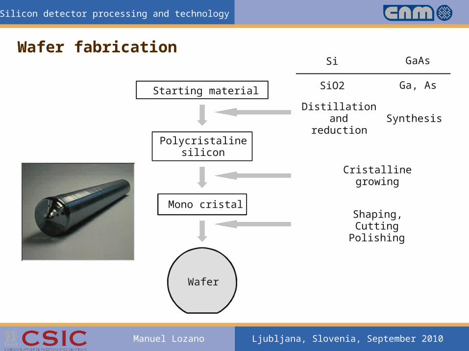
Wafer fabrication
Starting material
Polycristalinesilicon
Mono cristal
Wafer
Distillationand
reductionSynthesis
Cristallinegrowing
Shaping,Cutting
Polishing
Si
SiO2
GaAs
Ga, As

Ljubljana, Slovenia, September 2010
Silicon detector processing and technology
Manuel Lozano
Wafer fabrication: Czrochralsky Method
Pure silicon is melt in a crucible Pull Si crystal seed from the
melt, as Si solidifies, the crystalline orientation is kept.
Seed fixing
Seed
Crystal
Silicon crucible
Heather
Graphite
Melting
Liquid
Solid

Ljubljana, Slovenia, September 2010
Silicon detector processing and technology
Manuel Lozano
Wafer fabrication: Czrochralsky Method
Fused silicon is in contact with crucible: Dissolves oxygen from silica and also other impurities.
CZ-Silicon is not suitable for very low doping (<1013 cm-2), or conversely, for very high resistivities, as needed for particle detectors
CZ is the most common method used by IC industry, and therefore cheap (10 cm wafer < 50 €)
Use of magnetic fields can help in containing impurities far from solidifying surface. Since few years there are CZ available in sufficiently high purity (resistivity) to allow for use as particle detector. The technology is named Magnetic Czochrlasky (MCZ).

Ljubljana, Slovenia, September 2010
Silicon detector processing and technology
Manuel Lozano
Wafer fabrication: Float-zone Method
Silicon ingot is passed through a ring-shaped furnace. Silicon melts locally, impurities are segregated to the melted zone, and is purified.
Several passes are possible, achieving ultra high purity.
Polycristalline silicon
Oriented seed
Monocrystalline silicon
RF Heating Coil
Melted zone

Ljubljana, Slovenia, September 2010
Silicon detector processing and technology
Manuel Lozano
Epitaxial growth
Monocrystalline silicon growth over Si wafer. Growth rate about 1mm/min excellent homogeneity of resistivity
Main application: High resistivity silicon over low
resistivity substrate Highly doped buried layers (same or
different type) High temp. process
950 - 1250 ºC CZ silicon substrate used in-
diffusion of oxygen up to 150 mm thick layers produced price depending on thickness of epi-
layer but not exceeding 3 price of FZ wafer
C
x

Ljubljana, Slovenia, September 2010
Silicon detector processing and technology
Manuel Lozano
Images of wafer fabrication

Ljubljana, Slovenia, September 2010
Silicon detector processing and technology
Manuel Lozano
Silicon crystal lattice
X
Y
Z
(100)
(110)
(111)
X
Y
Z
X
Y
Z

Ljubljana, Slovenia, September 2010
Silicon detector processing and technology
Manuel Lozano
Wafer orientation
Primaryflat
Secondary flat
{111} N type {111} P type
{100} N type {100} P type
45º
180º
Secondaryflat
90º
Primaryflat
Primaryflat
Primaryflat
Secondary flat

Ljubljana, Slovenia, September 2010
Silicon detector processing and technology
Manuel Lozano
Doping-resistivity relationship (Thurber curves)
1.E+12
1.E+13
1.E+14
1.E+15
1.E+16
1.E+17
1.E+18
1.E+19
1.E+20
1.E+21
1.E-04 1.E-03 1.E-02 1.E-01 1.E+00 1.E+01 1.E+02 1.E+03
Resistivity ( cm)W
Do
pin
g (
cm
-3)
1.E+04
Boron
Phosphorus

Ljubljana, Slovenia, September 2010
Silicon detector processing and technology
Manuel Lozano
Resistivity variation
From wafer to wafer Intra wafer
Example: Surface resistiviy mapping of a MCZ wafer measured by 4-point probe method.
Ljubljana, Slovenia, September 2010
Silicon detector processing and technology
Manuel Lozano
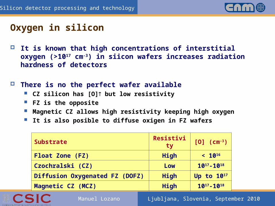
Oxygen in silicon
It is known that high concentrations of interstitial oxygen (>1017 cm-3) in siicon wafers increases radiation hardness of detectors
There is no the perfect wafer available CZ silicon has [O] but low resistivity FZ is the opposite Magnetic CZ allows high resistivity keeping high oxygen It is also posible to diffuse oxigen in FZ wafers
SubstrateResistivit
y[O] (cm-3)
Float Zone (FZ) High < 1016
Czochralski (CZ) Low 1017-1018
Diffusion Oxygenated FZ (DOFZ) High Up to 1017
Magnetic CZ (MCZ) High 1017-1018
Ljubljana, Slovenia, September 2010
Silicon detector processing and technology
Manuel Lozano
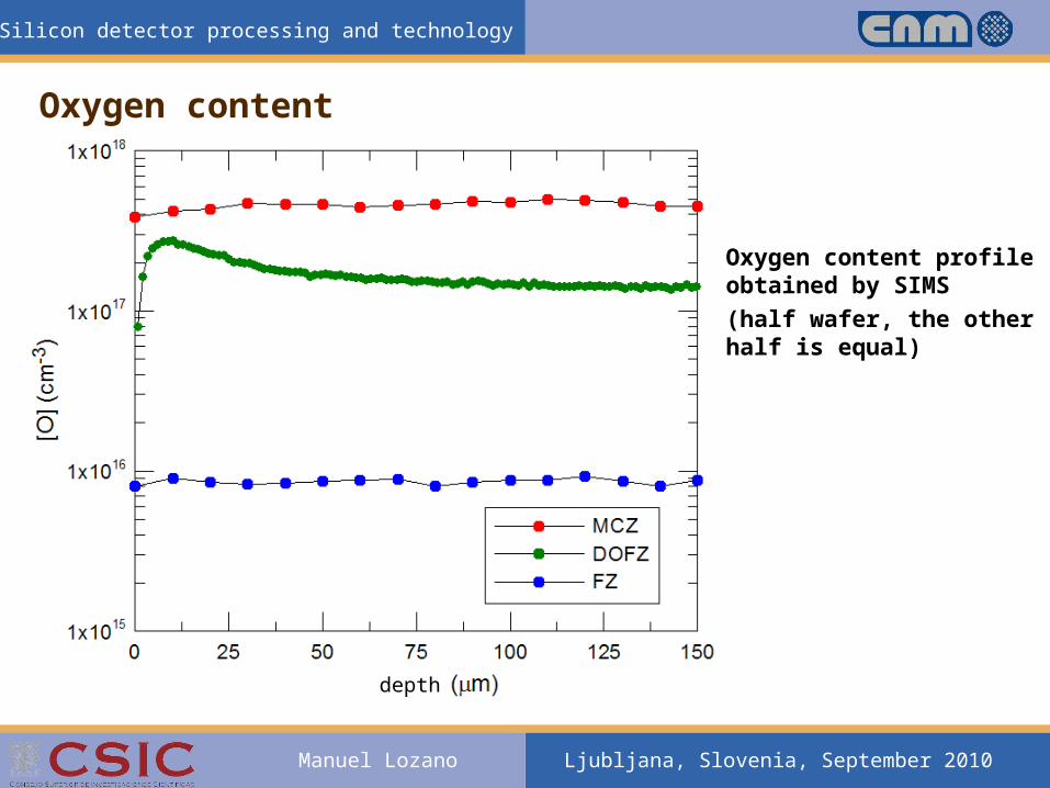
Oxygen content
Oxygen content profile obtained by SIMS(half wafer, the other half is equal)
depth
Ljubljana, Slovenia, September 2010
Silicon detector processing and technology
Manuel Lozano
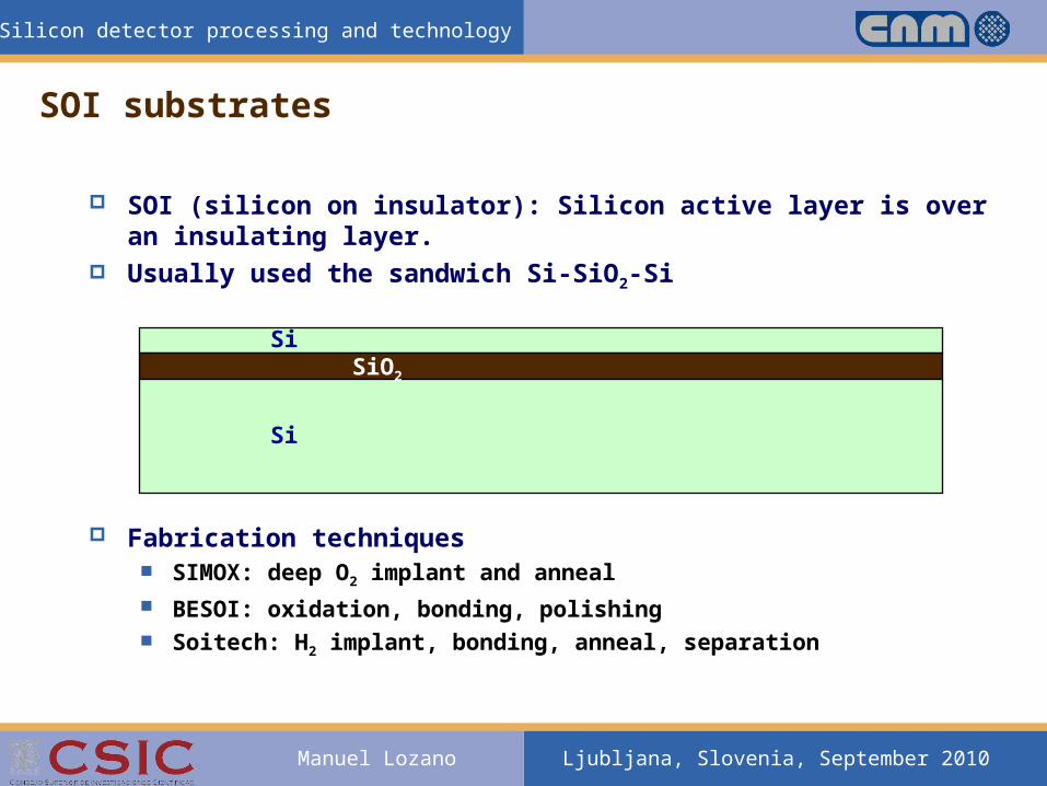
SOI substrates
SOI (silicon on insulator): Silicon active layer is over an insulating layer.
Usually used the sandwich Si-SiO2-Si
Fabrication techniques SIMOX: deep O2 implant and anneal BESOI: oxidation, bonding, polishing Soitech: H2 implant, bonding, anneal, separation
Si
SiSiO2

Ljubljana, Slovenia, September 2010
Silicon detector processing and technology
Manuel Lozano
SOI wafers
Can be tailored to the needs: Thickness of each wafer Thickness of intermediate
layer
Implanted wafers can be used Even with more complex
processing It is also possible to de-bond
wafers
Wafer 2
Wafer 1
Oxidize wafer 2
Bond wafers
Grind and polishwafers downtodesired thikness
Wafer 2with implanted layer
Wafer 1
Oxidize wafer 2
Bond wafers
Grind and polishwafers downtodesired thikness

Ljubljana, Slovenia, September 2010
Silicon detector processing and technology
Manuel Lozano
Dopant thermal diffusion
Atom movement within a solid at high temperatures.
Used to introduce dopants into semiconductor substrates (n+ and p+ regions)
Parameters: Diffusion coefficient of each
dopant into silicon Dopant Concentration,
Temperature and Time Dopant types
Acceptor (N-type): Boron Donor (N-type): Phosphorus,
Arsenic
Dopant sources: gas, liquid, solid

Ljubljana, Slovenia, September 2010
Silicon detector processing and technology
Manuel Lozano
Dopant thermal diffusion
A SiO2 mask can be used to limit dopant area Reproduce the mask on the wafer surface (SiO2 resistant to
high T and dopants diffusion) Apply the right concentration, temperature and time
Two possibilities: Dopants in ambient in constant concentration: Predeposition +
diffusion Dopant introduced in silicon: Implant + Drive-in

Ljubljana, Slovenia, September 2010
Silicon detector processing and technology
Manuel Lozano
Dopant thermal diffusion model
Analytical solution for the two cases presented
Dt
xCtxCCtC SS 2
0 erfc),(),(
Dtx
Dt
QtxCQdxtxC
4
2
exp),(),(
PredepositionConstant surface concentration
Ion implantConstant total charge

Ljubljana, Slovenia, September 2010
Silicon detector processing and technology
Manuel Lozano
Lateral diffusion Dopants diffuse below masks
lateral diffusion = 0.8 vertical diffusion

Ljubljana, Slovenia, September 2010
Silicon detector processing and technology
Manuel Lozano
Diffusion coefficients
Contamination concern: Na, Au.
Example: length diffused during 1 hour at 1000 ºC:
1.E-17
1.E-16
1.E-15
1.E-14
1.E-13
1.E-12
1.E-11
1.E-10
1.E-09
1.E-08
1.E-07
1.E-06
1.E-05
1.E-04
900 1000 1100 1200T (ºC)
D (
cm2/
s)
Sb
AsB
P
Au (S)
Au (I)
Fe
Al
Ga In
B 0.039 µm
P 0.065 µm
As 0.029 µm
O 2.4 µm
Au 300 µm
Na > 1,000 µm

Ljubljana, Slovenia, September 2010
Silicon detector processing and technology
Manuel Lozano
Furnace layout
Tube material: Quartz Polysilicon SiC
Wall Single Double
Ljubljana, Slovenia, September 2010
Silicon detector processing and technology
Manuel Lozano
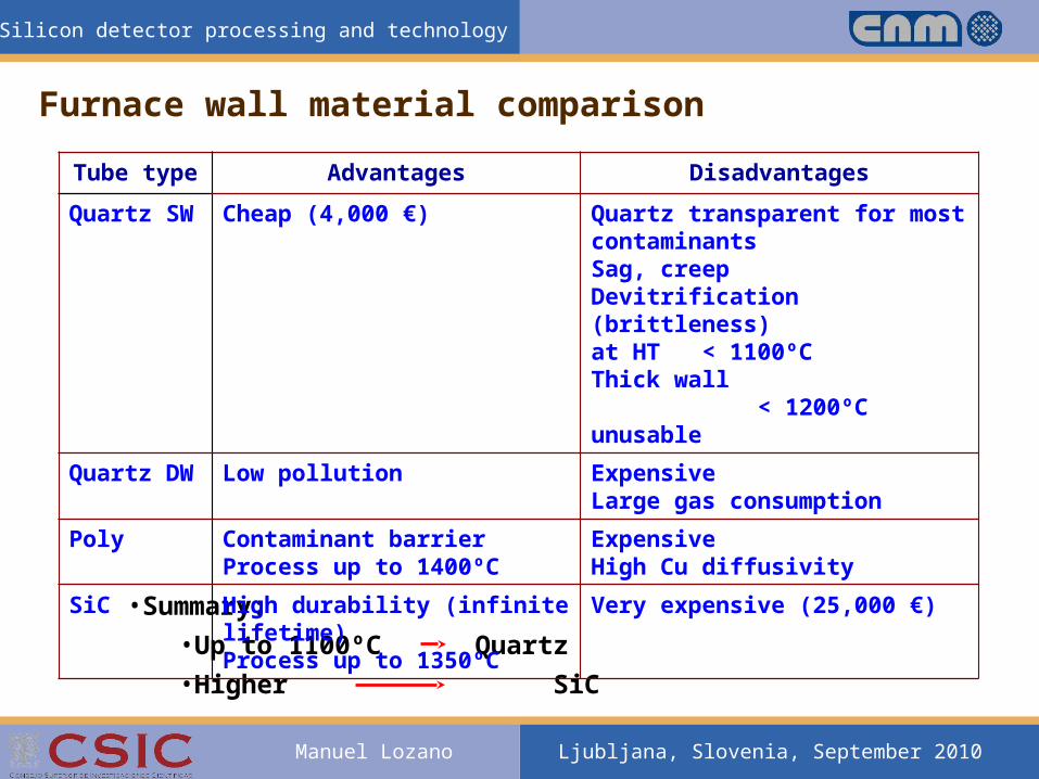
Furnace wall material comparison
•Summary:
•Up to 1100ºC Quartz
•Higher SiC
Tube type Advantages Disadvantages
Quartz SW Cheap (4,000 €) Quartz transparent for most contaminantsSag, creepDevitrification (brittleness)at HT < 1100ºC Thick wall < 1200ºC unusable
Quartz DW Low pollution ExpensiveLarge gas consumption
Poly Contaminant barrierProcess up to 1400ºC
ExpensiveHigh Cu diffusivity
SiC High durability (infinite lifetime)Process up to 1350ºC
Very expensive (25,000 €)

Ljubljana, Slovenia, September 2010
Silicon detector processing and technology
Manuel Lozano
Furnace images

Ljubljana, Slovenia, September 2010
Silicon detector processing and technology
Manuel Lozano
Thermal oxidation
SiO2 growing from silicon on the silicon
SiO2 is an amorphous material and very good insulator
High temperature process 950 - 1150 ºC
Used for: Mask for further thermal steps Insulating layer Gate dielectric oxide in MOS
devices SiO2 characterization
Density, porosity Pinholes Dielectric breakdown Trapped charge SiO2-Si interface states

Ljubljana, Slovenia, September 2010
Silicon detector processing and technology
Manuel Lozano
Thermal oxidation process
Same furnaces as for thermal diffusion
Dry thermal oxidation O2 atmosphere Slow growth High oxide quality
Wet thermal oxidation H2O atmosphere
H2O bubbler
H2+O2 combustion
Fast growing Worse quality
222
22
22 HSiOOHSi
SiOOSi

Ljubljana, Slovenia, September 2010
Silicon detector processing and technology
Manuel Lozano
Thermal oxidation model
Deal & Grove model
tdBA
dB oxox
21
BAdd
kTEABAB
kTEBB
ii
AB
B
2
0
0
)/exp()/(/
)/exp(
/
Dry oxidation
Wet oxidation

Ljubljana, Slovenia, September 2010
Silicon detector processing and technology
Manuel Lozano
Silicon thermal oxidation
Si S i
44%
56%2SiO
SiO2 grows consuming silicon substrate As opposite to deposition

Ljubljana, Slovenia, September 2010
Silicon detector processing and technology
Manuel Lozano
Relationship between diffusion and oxidation
Segregation coefficient k
k<1 Oxide takes impurities from substrate
k<1 Oxide rejects impurities to substrate

Ljubljana, Slovenia, September 2010
Silicon detector processing and technology
Manuel Lozano
Ion implant
Impurity introduction in substrates
Very well dose control Masking (SiO2 for instance) can be
used to delimit doping regions Method:
Ion (isotope) acceleration in an electric field
Parameters: Energy: 50 -250 keV (even 1MeV) Dose: 1011 – 1014 ions/cm2 (= current time)
Impurities N-type: As, P P-type: B Other elements: O, F, N, Ar

Ljubljana, Slovenia, September 2010
Silicon detector processing and technology
Manuel Lozano
Ion implant effect to be considered
Amorphization: After implant, crystal structure of Si is damaged.
Annealing is necessary (minimum 950ºC, 20 min)
Channeling: If implanting perpendicular to crystal structure, ions enter very deep without control
Wafer rotated and tilted
Uses: Junction formation Polysilicon doping Threshold voltage adjustment
Ion implanter schematic
Ljubljana, Slovenia, September 2010
Silicon detector processing and technology
Manuel Lozano
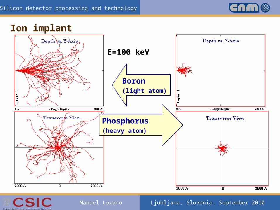
Ion implant
Boron(light atom)
Phosphorus(heavy atom)
E=100 keV

Ljubljana, Slovenia, September 2010
Silicon detector processing and technology
Manuel Lozano
CVD layer deposition
CVD: Chemical Vapor Deposition Layer deposition by chemical
reaction in vapor phase Mainly used for dielectric,s, but also
for Poly Main deposited materials:
Polysilicon, SiO2, Si2N3 , BSG, PSG, BPSG (SiO2 doped with B or P)
HTCVD: High Temperature LTCVD: Low Temperature PECVD: Plasma Enhanced LPCVD: Low Pressure APCVD: Atmospheric
Pressure

Ljubljana, Slovenia, September 2010
Silicon detector processing and technology
Manuel Lozano
CVD layer deposition
The substrate does not participate in the process Reaction of gas molecules on the surface
Reactions in the gas to be avoided Linear growth: there is no diffusion through a layer of
increasing thickness
Deposit velocity limited by: At high T, reactant
concentration (APCVD) At low P, surface reaction
velocity (LPCVD, PECVD)
As it is a surface reaction, layers offer good step coverage (conformal deposition)

Ljubljana, Slovenia, September 2010
Silicon detector processing and technology
Manuel Lozano
CVD layer deposition
Gas Type Pressure Temp Layer
SiH2Cl2 + NH3 LPCVD 160mTorr
800°C Nitride
SiH4 LPCVD 130mTorr
580 - 630°C Polysilicon
N2O, SiH4, NH3 PECVD 1Torr 380°C Oxide, nitride passivation
SiH4, PH3/SiH4, B2H6, O2
APCVD 400°C Interlevel oxide, PSG, BPSG
APCVD LPCVD PECVD
Simplicity + - --
Temperature
low medium low
Coverage - ++ +
Speed + - +

Ljubljana, Slovenia, September 2010
Silicon detector processing and technology
Manuel Lozano
CVD layer deposition
LPCVD poly deposition furnace

Ljubljana, Slovenia, September 2010
Silicon detector processing and technology
Manuel Lozano
CVD layer deposition
PECVD poly deposition furnace

Ljubljana, Slovenia, September 2010
Silicon detector processing and technology
Manuel Lozano
CVD layer deposition
1 µm Poly deposited in holesSee the good wall coverage
1.5 µm BPSG depositedPlanarization effect

Ljubljana, Slovenia, September 2010
Silicon detector processing and technology
Manuel Lozano
PVD metal layer deposition
Metal deposition Techniques
Evaporation Sputtering
Multicomponent Co-sputtering Co-evaporation
Problems with metals: Spiking Electromigration
Metal used: Al, Al/Si, Al/Cu, Al/Si/Cu, Au,
Pt, W, Pd, Ti, Ta, Ni Multilayer metallization
possible

Ljubljana, Slovenia, September 2010
Silicon detector processing and technology
Manuel Lozano
Sputtering: Ion or electron bombardment of target to extract atoms

Ljubljana, Slovenia, September 2010
Silicon detector processing and technology
Manuel Lozano
Evaporation: target heating to evaporate (actually sublimate) the metal and re-deposition on wafer surface (colder than target) Difficult thickness control, contamination by crucible and coil
metals, hard to deposit alloys
Sputtering: Ion or electron bombardment of target to extract atoms Good thickness control and good layer quality

Ljubljana, Slovenia, September 2010
Silicon detector processing and technology
Manuel Lozano
Al spikes
p-n junction
Si - (100)
Al
SiO2
Spiking is due to dissolution of Si into Al and Al into Si and is related to the phase diagram.
Minimized by using Al/Si alloy and adjusting sintering temperature
Metal problems
Electromigration: material movement due to kinetic energy of charge carriers. Eventually can open circuit a metallic track Probability is proportional to current density,
temperature and time Minimized by using Al/Cu alloy
Spiking: Al penetration in substrate and eventually shorting the junction

Ljubljana, Slovenia, September 2010
Silicon detector processing and technology
Manuel Lozano
Photolithography
Image transfer from a glass mask to the wafer
Employs UV light Masks or reticles Photoresist
Types Contact/proximity
Resolution: 2um Projection
Resolution: 1 um
Better resolution Deep UV X rays Electron beam
UV
Mask
Substrate
LayerPhotoresist

Ljubljana, Slovenia, September 2010
Silicon detector processing and technology
Manuel Lozano
Photolithography types
Ljubljana, Slovenia, September 2010
Silicon detector processing and technology
Manuel Lozano
Photolithography masks
Layout: final geometrical drawings resulting from a design process for a target technology
Layers: all the different basic drawing levels to design ICs for a target technology
Masks: clear and opaque areas over a glass obtained from layers to transfer over and process the wafers.
Mask material Quartz and Chromium (with ARC)
n+p+
polymetalcontactn-well
Layout Layers
MasksA/A
nplus pplusnwell
polySi
contact
metall
MasksA/A
nplus pplusnwell
polySi
contact
metall
Ljubljana, Slovenia, September 2010
Silicon detector processing and technology
Manuel Lozano
Photolithography process Coating wafer with thin film photoresist Mask-Wafer Alignment UV Exposure Photoresist Development Etching/implant/etc. Photoresist removal
Positive process Negative process

Ljubljana, Slovenia, September 2010
Silicon detector processing and technology
Manuel Lozano
Photolithography process: Other key points
Negative vs. positive photoresists
Relationship between virtual layout and phisical mask Dark field, light field Right reading, wrong reading
layout Light field Dark field
Right reading Wrong reading
For masks to be used in the back side of the wafer. Two side processing

Ljubljana, Slovenia, September 2010
Silicon detector processing and technology
Manuel Lozano
Photolithography process: Other key points
Projection lithography (Step and repeat) Better resolution Limited chip surface (2525 mm
maximum)
Alignment marks Very important Clear chips: Critical in layers “all
dark” as contact opening
Dark Field
Dar
k F
ield
Light Field
Bottom layer (mark in wafer)
Top
laye
r (m
ask
bein
g al
igne
d)
Ligh
t Fi
eld

Ljubljana, Slovenia, September 2010
Silicon detector processing and technology
Manuel Lozano
Etching
Selectively remove of previously deposited material from top of wafers.
Parameters: Selectivity(For example: SiO2 should be
attacked but not photoresist and silicon)
Degree of Anisotropy (attack direction) Process:
Purely chemical vs. P. Physical (Selectivity vs. Anisotropy)
Wet Etching: wafers are exposed to liquid chemicals
Dry Etching: wafers are chemically etched in a gas at reduced pressure

Ljubljana, Slovenia, September 2010
Silicon detector processing and technology
Manuel Lozano
Wet etching
Etching with wet chemical agents
Used: to: Surface cleaning Complete removal of layers Selective etching of layers
Examples: Cleaning: H2SO4, H2O, HCl SiO2: HF + NH4F Polysilicon: HF + HNO3 Al: H3PO4
Needed: High selectivity High etching rate
Characteristics: Isotrope profile Easy control Dimension losses No end point detection

Ljubljana, Slovenia, September 2010
Silicon detector processing and technology
Manuel Lozano
Dry etching: Reactive Ion Etching (RIE) RIE (also known as plasma etching) is a technique developed
in the 80’s which combines simultaneous chemical and physical etching.
Chemical reactants are excited to become a plasma by RF capacitively coupled and also accelerated in an electric field.
Anisotropic
Isotropic
C h e m ic a l re a c tio n+
P h y s ic a l e tc h in g
inert speciesre-deposition
ions
Different degrees of anisotropy can be obtained modifying gas concentrations, pressure, RF power
Some degree of re-deposition in the sidewalls which act as passivation allow finer control of etching profiles
End point control possible by monitoring gas reactions

Ljubljana, Slovenia, September 2010
Silicon detector processing and technology
Manuel Lozano
Anisotropic Si etching
Etching through preferential crystalline planes V(110)>V(100)>V(111)
Wet etching with alcalis KOH TMAH (Tetra Metil Hydroxi
Ammonia)

Ljubljana, Slovenia, September 2010
Silicon detector processing and technology
Manuel Lozano
Anisotropic Si etching
Difficulty: Etch stop at the required depth Stopping techniques:
Time Inner layer Highly doped P+ layer Electrochemical: requires complex setup
Time ElectrochemicalHighly doped
P+ layerInner layer
(SOI for example)