hardware data sheet section iii et1815 / et1816 … · hardware data sheet section iii et1815 /...
TRANSCRIPT
Version 1.0 Date: 2015-01-20
Hardware Data Sheet Section III ET1815 / ET1816
Slave Controller IP Core for Xilinx® FPGAs Release 3.00k Section I – Technology (Online at http://www.beckhoff.com)
Section II – Register Description (Online at http://www.beckhoff.com)
Section III – Hardware Description Installation, Configuration, Resource
consumption, Interface specification
DOCUMENT ORGANIZATION
III-II Slave Controller – IP Core for Xilinx FPGAs
DOCUMENT ORGANIZATION
The Beckhoff EtherCAT Slave Controller (ESC) documentation covers the following Beckhoff ESCs:
ET1200
ET1100
EtherCAT IP Core for Altera® FPGAs
EtherCAT IP Core for Xilinx® FPGAs
ESC20
The documentation is organized in three sections. Section I and section II are common for all Beckhoff ESCs, Section III is specific for each ESC variant.
The latest documentation is available at the Beckhoff homepage (http://www.beckhoff.com).
Section I – Technology (All ESCs)
Section I deals with the basic EtherCAT technology. Starting with the EtherCAT protocol itself, the frame processing inside EtherCAT slaves is described. The features and interfaces of the physical layer with its two alternatives Ethernet and EBUS are explained afterwards. Finally, the details of the functional units of an ESC like FMMU, SyncManager, Distributed Clocks, Slave Information Interface, Interrupts, Watchdogs, and so on, are described.
Since Section I is common for all Beckhoff ESCs, it might describe features which are not available in a specific ESC. Refer to the feature details overview in Section III of a specific ESC to find out which features are available.
Section II – Register Description (All ESCs)
Section II contains detailed information about all ESC registers. This section is also common for all Beckhoff ESCs, thus registers, register bits, or features are described which might not be available in a specific ESC. Refer to the register overview and to the feature details overview in Section III of a specific ESC to find out which registers and features are available.
Section III – Hardware Description (Specific ESC)
Section III is ESC specific and contains detailed information about the ESC features, implemented registers, configuration, interfaces, pinout, usage, electrical and mechanical specification, and so on. Especially the Process Data Interfaces (PDI) supported by the ESC are part of this section.
Additional Documentation
Application notes and utilities can also be found at the Beckhoff homepage. Pinout configuration tools for ET1100/ET1200 are available. Additional information on EtherCAT IP Cores with latest updates regarding design flow compatibility, FPGA device support and known issues are also available.
Trademarks Beckhoff®, TwinCAT®, EtherCAT®, Safety over EtherCAT®, TwinSAFE® and XFC® are registered trademarks of and licensed by Beckhoff Automation GmbH & Co. KG. Other designations used in this publication may be trademarks whose use by third parties for their own purposes could violate the rights of the owners.
Patent Pending The EtherCAT Technology is covered, including but not limited to the following German patent applications and patents: DE10304637, DE102004044764, DE102005009224, DE102007017835 with corresponding applications or registrations in various other countries.
Disclaimer The documentation has been prepared with care. The products described are, however, constantly under development. For that reason the documentation is not in every case checked for consistency with performance data, standards or other characteristics. In the event that it contains technical or editorial errors, we retain the right to make alterations at any time and without warning. No claims for the modification of products that have already been supplied may be made on the basis of the data, diagrams and descriptions in this documentation.
Copyright © Beckhoff Automation GmbH & Co. KG 01/2015. The reproduction, distribution and utilization of this document as well as the communication of its contents to others without express authorization are prohibited. Offenders will be held liable for the payment of damages. All rights reserved in the event of the grant of a patent, utility model or design.
DOCUMENT HISTORY
Slave Controller – IP Core for Xilinx FPGAs III-III
DOCUMENT HISTORY
Version Comment
1.0 Initial release EtherCAT IP Core for Xilinx FPGAs v3.00k

CONTENTS
III-IV Slave Controller – IP Core for Xilinx FPGAs
CONTENTS
1 Overview 1
1.1 Frame processing order 2
1.2 Scope of this document 3
1.3 Scope of Delivery 3
1.4 Target FPGAs 4
1.5 Designflow requirements 4
1.6 Tested FPGA/Designflow combinations 5
1.7 Release Notes 6
1.7.1 Major differences between V2.04x and V3.00x 9
1.7.2 Reading IP Core version from device 9
1.8 Design flow 10
1.9 IP Core Evaluation 11
1.10 Simulation 12
2 Features and Registers 13
2.1 Features 13
2.2 Registers 16
2.3 Extended ESC Features in User RAM 19
3 IP Core Installation 23
3.1 Installation on Windows PCs 23
3.1.1 System Requirements 23
3.1.2 Installation 23
3.2 Installation on Linux PCs 24
3.2.1 System Requirements 24
3.2.2 Installation 24
3.3 Files located in the lib folder 24
3.4 License File 25
3.5 IP Core Vendor ID Package 25
3.6 RSA Decryption Keys 26
3.7 Environment Variable 26
3.8 Integrating the EtherCAT IP Core into the Xilinx Designflow 27
3.8.1 Software Templates for example designs with Microblaze/ARM processor (EDK) 27
3.8.2 Software Templates for example designs with ARM processor (Vivado) 27
3.9 EtherCAT Slave Information (ESI) / XML device description for example designs 27
4 IP Core Usage 28
4.1 IPCore_Config Tool 28
4.2 EDK designs with EtherCAT IP Core 29
4.3 Vivado designs with EtherCAT IP Core 33
5 IP Core Configuration 34
5.1.1 Product ID tab 35

CONTENTS
Slave Controller – IP Core for Xilinx FPGAs III-V
5.1.2 Physical Layer tab 36
5.1.3 Internal Functions tab 38
5.1.4 Feature Details tab 40
5.1.5 Register: Process Data Interface tab 42
6 Example Designs 49
6.1 Avnet Xilinx Spartan-6 LX150T Development Kit with Digital I/O 50
6.1.1 Configuration and resource consumption 50
6.1.2 Functionality 50
6.1.3 Implementation 50
6.1.4 SII EEPROM 51
6.1.5 Downloadable configuration file 51
6.2 Avnet Xilinx Spartan-6 LX150T Development Kit with AXI 52
6.2.1 Configuration and resource consumption 52
6.2.2 Functionality 52
6.2.3 Implementation 53
6.2.4 SII EEPROM 53
6.2.5 Downloadable configuration file 53
6.3 Xilinx Zynq ZC702 Development Kit with AXI (Vivado based) 54
6.3.1 Configuration and resource consumption 54
6.3.2 Functionality 54
6.3.3 Implementation 55
6.3.4 SII EEPROM 55
7 FPGA Resource Consumption 56
8 IP Core Signals 59
8.1 General Signals 59
8.1.1 Clock source example schematics 60
8.2 SII EEPROM Interface Signals 61
8.3 LED Signals 61
8.4 Distributed Clocks SYNC/LATCH Signals 62
8.5 Physical Layer Interface 63
8.5.1 MII Interface 64
8.5.2 RMII Interface 66
8.5.3 RGMII Interface 67
8.6 PDI Signals 70
8.6.1 General PDI Signals 70
8.6.2 Digital I/O Interface 70
8.6.3 SPI Slave Interface 71
8.6.4 Asynchronous 8/16 Bit µController Interface 71
8.6.5 PLB Processor Local Bus 73
8.6.6 AXI4 / AXI4 LITE On-Chip Bus 76
9 Ethernet Interface 78
CONTENTS
III-VI Slave Controller – IP Core for Xilinx FPGAs
9.1 PHY Management interface 78
9.1.1 PHY Management Interface Signals 78
9.1.2 PHY Address Configuration 78
9.1.3 Separate external MII management interfaces 79
9.1.4 MII management timing specifications 79
9.2 MII Interface 80
9.2.1 MII Interface Signals 81
9.2.2 TX Shift Compensation 82
9.2.3 MII Timing specifications 83
9.2.4 MII example schematic 84
9.3 RMII Interface 85
9.3.1 RMII Interface Signals 85
9.3.2 RMII example schematic 86
9.4 RGMII Interface 87
9.4.1 RGMII Interface Signals 87
9.4.2 RGMII example schematic 89
9.4.3 RGMII RX timing options 89
9.4.4 RGMII TX timing options 89
10 PDI Description 91
10.1 Digital I/O Interface 92
10.1.1 Interface 92
10.1.2 Configuration 93
10.1.3 Digital Inputs 93
10.1.4 Digital Outputs 93
10.1.5 Output Enable 94
10.1.6 SyncManager Watchdog 94
10.1.7 SOF 95
10.1.8 OUTVALID 95
10.1.9 Timing specifications 95
10.2 SPI Slave Interface 98
10.2.1 Interface 98
10.2.2 Configuration 98
10.2.3 SPI access 99
10.2.4 Address modes 99
10.2.5 Commands 100
10.2.6 Interrupt request register (AL Event register) 100
10.2.7 Write access 100
10.2.8 Read access 100
10.2.9 SPI access errors and SPI status flag 101
10.2.10 2 Byte and 4 Byte SPI Masters 102
10.2.11 Timing specifications 103

CONTENTS
Slave Controller – IP Core for Xilinx FPGAs III-VII
10.3 Asynchronous 8/16 bit µController Interface 109
10.3.1 Interface 109
10.3.2 Configuration 109
10.3.3 µController access 110
10.3.4 Write access 110
10.3.5 Read access 110
10.3.6 µController access errors 111
10.3.7 Connection with 16 bit µControllers without byte addressing 111
10.3.8 Connection with 8 bit µControllers 112
10.3.9 Timing Specification 113
10.4 PLB Slave Interface 117
10.4.1 Interface 117
10.4.2 Configuration 118
10.4.3 Timing specifications 119
10.5 AXI4/AXI4 LITE On-Chip Bus 121
10.5.1 Interface 121
10.5.2 Configuration 123
10.5.3 Interrupts 123
10.5.4 Timing specifications 124
11 Distributed Clocks SYNC/LATCH Signals 126
11.1 Signals 126
11.2 Timing specifications 126
12 SII EEPROM Interface (I²C) 127
12.1 Signals 127
12.2 EEPROM Emulation 127
12.3 Timing specifications 127
13 Electrical Specifications 128
14 Synthesis Constraints 129
15 Appendix 132
15.1 Support and Service 132
15.1.1 Beckhoff’s branch offices and representatives 132
15.2 Beckhoff Headquarters 132
TABLES
III-VIII Slave Controller – IP Core for Xilinx FPGAs
TABLES
Table 1: IP Core Main Features .............................................................................................................. 1 Table 2: Frame Processing Order ........................................................................................................... 2 Table 3: Tested FPGA/Designflow combinations .................................................................................... 5 Table 4: Release notes ............................................................................................................................ 6 Table 5: Register Revision (0x0001) ....................................................................................................... 9 Table 6: Register Build (0x0002:0x0003) ................................................................................................ 9 Table 7: IP Core Feature Details ........................................................................................................... 13 Table 8: Legend ..................................................................................................................................... 15 Table 9: Register availability.................................................................................................................. 16 Table 10: Legend ................................................................................................................................... 18 Table 11: Extended ESC Features (Reset values of User RAM – 0x0F80:0x0FFF) ............................ 19 Table 12: Contents of lib folder.............................................................................................................. 24 Table 13: Resource consumption Avnet LX150T example design ....................................................... 50 Table 14: Resource consumption Avnet LX150T example design ....................................................... 52 Table 15: Resource consumption Xilinx Zynq ZC702 example design ................................................. 54 Table 16: Approximate resource requirements for main configurable functions ................................... 57 Table 17: EtherCAT IP Core resource consumption for typical EtherCAT Devices .............................. 58 Table 18: General Signals ..................................................................................................................... 59 Table 19: SII EEPROM Signals ............................................................................................................. 61 Table 20: LED Signals ........................................................................................................................... 61 Table 21: DC SYNC/LATCH signals ..................................................................................................... 62 Table 22: Physical Layer General ......................................................................................................... 63 Table 23: PHY Interface MII .................................................................................................................. 64 Table 24: PHY Interface RMII................................................................................................................ 66 Table 25: PHY Interface RGMII ............................................................................................................. 67 Table 26: General PDI Signals .............................................................................................................. 70 Table 27: Digital I/O PDI ........................................................................................................................ 70 Table 28: SPI PDI .................................................................................................................................. 71 Table 29: 8/16 Bit µC PDI ...................................................................................................................... 71 Table 30: 8 Bit µC PDI ........................................................................................................................... 72 Table 31: 16 Bit µC PDI ......................................................................................................................... 72 Table 32: PLB PDI ................................................................................................................................. 73 Table 33: PLB PDI additional signals of XPS/EDK pcores ................................................................... 75 Table 34: AXI4 / AXI4 LITE PDI ............................................................................................................ 76 Table 35: AXI4 / AXI4 LITE PDI additional signals of XPS/EDK pcores ............................................... 77 Table 36: PHY management Interface signals ...................................................................................... 78 Table 37: MII management timing characteristics ................................................................................. 79 Table 38: MII Interface signals .............................................................................................................. 81 Table 39: MII TX Timing characteristics ................................................................................................ 83 Table 40: MII timing characteristics ....................................................................................................... 83 Table 41: RMII Interface signals ............................................................................................................ 85 Table 42: RGMII Interface signals ......................................................................................................... 88 Table 43: Available PDIs for EtherCAT IP Core .................................................................................... 91 Table 44: IP core digital I/O signals ....................................................................................................... 92 Table 45: Input/Output byte reference ................................................................................................... 92 Table 46: Digital I/O timing characteristics IP Core ............................................................................... 95 Table 47: SPI signals ............................................................................................................................. 98 Table 48: Address modes ...................................................................................................................... 99 Table 49: SPI commands CMD0 and CMD1 ....................................................................................... 100 Table 50: Interrupt request register transmission ................................................................................ 100 Table 51: Write access for 2 and 4 Byte SPI Masters ......................................................................... 102 Table 52: SPI timing characteristics IP Core ....................................................................................... 103 Table 53: Read/Write timing diagram symbols .................................................................................... 104 Table 54: µController signals ............................................................................................................... 109 Table 55: 8 bit µController interface access types .............................................................................. 110 Table 56: 16 bit µController interface access types ............................................................................ 110 Table 57: µController timing characteristics IP Core ........................................................................... 113 Table 58: PLB signals .......................................................................................................................... 117 Table 59: PLB clock period values for synchronous clocking ............................................................. 118 Table 60: PLB timing characteristics ................................................................................................... 119
TABLES
Slave Controller – IP Core for Xilinx FPGAs III-IX
Table 61: AXI4 LITE signals ................................................................................................................ 121 Table 62: Additional AXI4 signals ........................................................................................................ 122 Table 63: AXI timing characteristics .................................................................................................... 124 Table 64: Distributed Clocks signals ................................................................................................... 126 Table 65: DC SYNC/LATCH timing characteristics IP Core ............................................................... 126 Table 66: I²C EEPROM signals ........................................................................................................... 127 Table 67: EEPROM timing characteristics IP Core ............................................................................. 127 Table 68: AC Characteristics ............................................................................................................... 128 Table 69: Forwarding Delays ............................................................................................................... 128 Table 70: EtherCAT IP Core constraints ............................................................................................. 129
FIGURES
III-X Slave Controller – IP Core for Xilinx FPGAs
FIGURES
Figure 1: EtherCAT IP Core Block Diagram ............................................................................................ 1 Figure 2: Frame Processing .................................................................................................................... 2 Figure 3: Design flow ............................................................................................................................. 10 Figure 4: Files installed with EtherCAT IP core setup ........................................................................... 23 Figure 5: IPCore_Config Open Menu .................................................................................................... 28 Figure 6: IP Core generation successful ............................................................................................... 28 Figure 7: EDK – Overview ..................................................................................................................... 30 Figure 8: EDK – Configuration of IP Core ............................................................................................. 30 Figure 9: EDK – Configuration Dialog ................................................................................................... 31 Figure 10: EDK – System Assembly View, Addresses tab ................................................................... 31 Figure 11: EDK – System Assembly View, Ports tab ............................................................................ 32 Figure 12: EtherCAT IP Core Configuration Interface ........................................................................... 34 Figure 13: Product ID tab ...................................................................................................................... 35 Figure 14: Physical Layer tab ................................................................................................................ 36 Figure 15: Internal Functions tab ........................................................................................................... 38 Figure 16: Feature Details tab ............................................................................................................... 40 Figure 17: Available PDI Interfaces ....................................................................................................... 42 Figure 18: Register Process Data Interface .......................................................................................... 43 Figure 19: Register PDI – Digital I/O Configuration............................................................................... 44 Figure 20: Register PDI – µC-Configuration.......................................................................................... 45 Figure 21: Register PDI – SPI Configuration ......................................................................................... 46 Figure 22: Register PDI – PLB Interface Configuration ........................................................................ 47 Figure 23: Register PDI – AXI4/AXI4 LITE Interface Configuration ...................................................... 48 Figure 24: EtherCAT IP Core clock source (MII) ................................................................................... 60 Figure 25: EtherCAT IP Core clock source (RMII) ................................................................................ 60 Figure 26: EtherCAT IP Core clock source (RGMII) ............................................................................. 60 Figure 27: PHY management Interface signals..................................................................................... 78 Figure 28: Example schematic with two individual MII management interfaces ................................... 79 Figure 29: MII Interface signals ............................................................................................................. 81 Figure 30: MII TX Timing Diagram ........................................................................................................ 82 Figure 31: MII timing RX signals............................................................................................................ 83 Figure 32: MII example schematic......................................................................................................... 84 Figure 33: RMII Interface signals........................................................................................................... 85 Figure 34: RMII example schematic ...................................................................................................... 86 Figure 35: RGMII Interface signals ........................................................................................................ 88 Figure 36: RGMII example schematic ................................................................................................... 89 Figure 37: IP core digital I/O signals ..................................................................................................... 92 Figure 38: Digital Output Principle Schematic ....................................................................................... 94 Figure 39: Digital Input: Input data sampled at SOF, I/O can be read in the same frame .................... 96 Figure 40: Digital Input: Input data sampled with LATCH_IN ................................................................ 96 Figure 41: Digital Input: Input data sampled with SYNC0/1 .................................................................. 96 Figure 42: Digital Output timing ............................................................................................................. 97 Figure 43: OUT_ENA timing .................................................................................................................. 97 Figure 44: SPI master and slave interconnection.................................................................................. 98 Figure 45: Basic SPI_DI/SPI_DO timing (*refer to timing diagram for relevant edges of SPI_CLK) .. 104 Figure 46: SPI read access (2 byte addressing, 1 byte read data) with Wait State byte .................... 105 Figure 47: SPI read access (2 byte addressing, 2 byte read data) with Wait State byte .................... 106 Figure 48: SPI write access (2 byte addressing, 1 byte write data) .................................................... 107 Figure 49: SPI write access (3 byte addressing, 1 byte write data) .................................................... 108 Figure 50: µController interconnection ................................................................................................ 109 Figure 51: Connection with 16 bit µControllers without byte addressing ............................................ 111 Figure 52: Connection with 8 bit µControllers (BHE and DATA[15:8] should not be left open) .......... 112 Figure 53: Read access (without preceding write access) .................................................................. 114 Figure 54: Write access (write after rising edge nWR, without preceding write access) .................... 115 Figure 55: Sequence of two write accesses and a read access ......................................................... 115 Figure 56: Write access (write after falling edge nWR) ....................................................................... 116 Figure 57: PLB signals ........................................................................................................................ 117 Figure 58: PLB Read Access .............................................................................................................. 120 Figure 59: PLB Write Access ............................................................................................................... 120 Figure 60: AXI4 signals ....................................................................................................................... 121

FIGURES
Slave Controller – IP Core for Xilinx FPGAs III-XI
Figure 61: AXI Read Access ............................................................................................................... 125 Figure 62: AXI Write Access ................................................................................................................ 125 Figure 63: Distributed Clocks signals .................................................................................................. 126 Figure 64: LatchSignal timing .............................................................................................................. 126 Figure 65: SyncSignal timing ............................................................................................................... 126 Figure 66: I²C EEPROM signals .......................................................................................................... 127
ABBREVIATIONS
III-XII Slave Controller – IP Core for Xilinx FPGAs
ABBREVIATIONS
µC Microcontroller ADR Address AL Application Layer AMBA® Advanced Microcontroller Bus Architecture from ARM® AXITM Advanced eXtensible Interface Bus, an AMBA interconnect. Used as On-Chip-bus BHE Bus High Enable BSP Board Support Package CMD Command CS Chip Select DC Distributed Clock DCM Digital Clock Manager DL Data Link Layer ECAT EtherCAT EDK Embedded Development Kit (Xilinx software) EOF End of Frame ESC EtherCAT Slave Controller ESI EtherCAT Slave Information FMMU Fieldbus Memory Management Unit FPGA Field Programmable Gate Array GPI General Purpose Input GPO General Purpose Output HDL Hardware Description Language IP Intellectual Property IRQ Interrupt Request ISE Integrated Software Environment (Xilinx software) LE Logic Element LC Logic Cell MAC Media Access Controller MDIO Management Data Input / Output MHS Microprocessor Hardware Specification MI (PHY) Management Interface MII Media Independent Interface MISO Master In – Slave Out MOSI Master Out – Slave In MPD Microprocessor Peripheral Specification OPB On-Chip Peripheral Bus PAO Peripheral Analyze Order PDI Process Data Interface PLB Processor Local Bus PLD Programmable Logic Device PLL Phase Locked Loop RBF Raw Binary File RD Read RMII Reduced Media Independent Interface SDK Software Development Kit SM SyncManager SoC System on a Chip SOF Start of Frame SOPC System on a programmable Chip SPI Serial Peripheral Interface VHDL Very High Speed Integrated Circuit Hardware Description Language WR Write
Overview
Slave Controller – IP Core for Xilinx FPGAs III-1
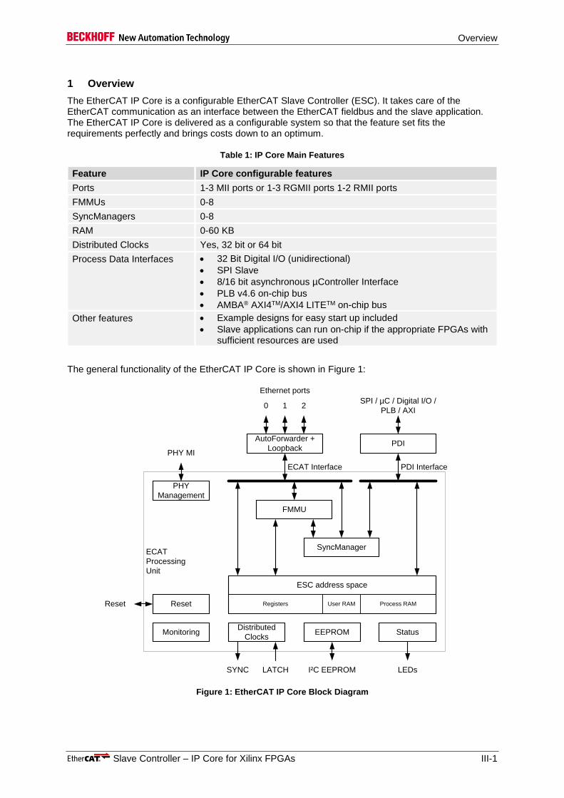
1 Overview
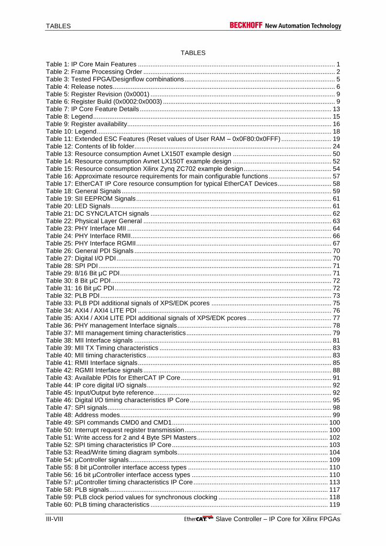
The EtherCAT IP Core is a configurable EtherCAT Slave Controller (ESC). It takes care of the EtherCAT communication as an interface between the EtherCAT fieldbus and the slave application. The EtherCAT IP Core is delivered as a configurable system so that the feature set fits the requirements perfectly and brings costs down to an optimum.
Table 1: IP Core Main Features
Feature IP Core configurable features
Ports 1-3 MII ports or 1-3 RGMII ports 1-2 RMII ports
FMMUs 0-8
SyncManagers 0-8
RAM 0-60 KB
Distributed Clocks Yes, 32 bit or 64 bit
Process Data Interfaces 32 Bit Digital I/O (unidirectional)
SPI Slave
8/16 bit asynchronous µController Interface
PLB v4.6 on-chip bus
AMBA® AXI4TM/AXI4 LITETM on-chip bus
Other features Example designs for easy start up included
Slave applications can run on-chip if the appropriate FPGAs with sufficient resources are used
The general functionality of the EtherCAT IP Core is shown in Figure 1:
ECAT
Processing
Unit
AutoForwarder +
Loopback
SyncManager
FMMU
ESC address space
User RAMRegisters Process RAM
EEPROMDistributed
ClocksMonitoring Status
PHY
Management
SYNC LEDsI²C EEPROM
PHY MI
SPI / µC / Digital I/O /
PLB / AXI0 2
Ethernet ports
LATCH
PDI
ECAT Interface PDI Interface
ResetReset
1
Figure 1: EtherCAT IP Core Block Diagram
Overview
III-2 Slave Controller – IP Core for Xilinx FPGAs
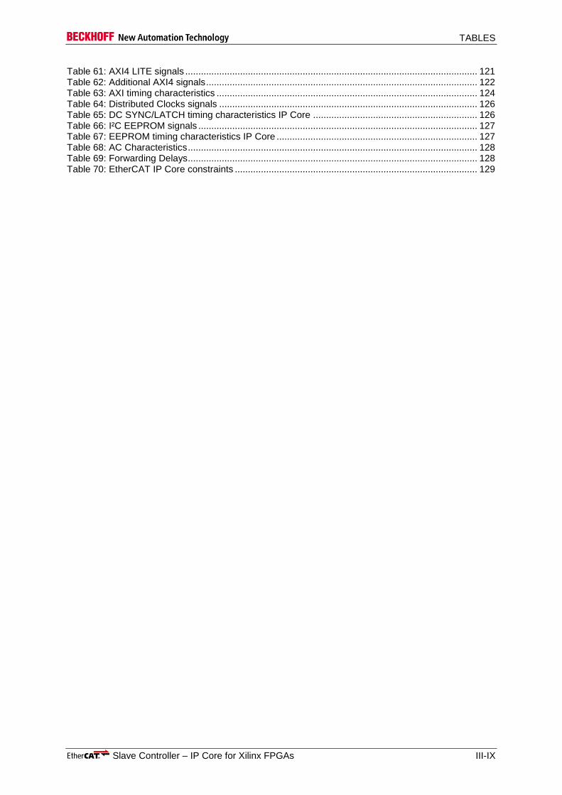
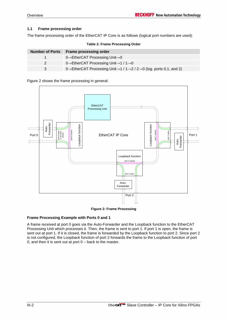
1.1 Frame processing order
The frame processing order of the EtherCAT IP Core is as follows (logical port numbers are used):
Table 2: Frame Processing Order
Number of Ports Frame processing order
1 0→EtherCAT Processing Unit→0
2 0→EtherCAT Processing Unit→1 / 1→0
3 0→EtherCAT Processing Unit→1 / 1→2 / 2→0 (log. ports 0,1, and 2)
Figure 2 shows the frame processing in general:
1Port 1
Au
to-
Fo
rwa
rde
rPort 0
Au
to-
Fo
rwa
rde
r
Lo
op
ba
ck fu
nctio
n
EtherCAT
Processing Unit
Lo
op
ba
ck fu
nctio
n
EtherCAT IP Core
po
rt 1
clo
se
d
po
rt 1
op
en
po
rt 0
op
en
or
all
po
rts
clo
se
d
po
rt 0
clo
se
d
Port 2
Auto-
Forwarder
Loopback function
port 2 closed
port 2 open
Figure 2: Frame Processing
Frame Processing Example with Ports 0 and 1
A frame received at port 0 goes via the Auto-Forwarder and the Loopback function to the EtherCAT Processing Unit which processes it. Then, the frame is sent to port 1. If port 1 is open, the frame is sent out at port 1. If it is closed, the frame is forwarded by the Loopback function to port 2. Since port 2 is not configured, the Loopback function of port 2 forwards the frame to the Loopback function of port 0, and then it is sent out at port 0 – back to the master.

Overview
Slave Controller – IP Core for Xilinx FPGAs III-3
1.2 Scope of this document
Purpose of this document is to describe the installation and configuration of the EtherCAT IP Core for Xilinx FPGAs. Furthermore, the signals and registers of the IP Core depending on the chosen configuration are described.
This documentation was made with the assumption that the user is familiar with the handling of the Xilinx Development Environment.
1.3 Scope of Delivery
The EtherCAT IP Core installation file includes:
EtherCAT IP Core (encrypted VHDL library)
Decryption keys for encrypted EtherCAT IP Core
IP Core Configuration Tool (IPCore_Config.exe)
Example designs
The following files which contain customer specific information are required to synthesize the IP Core. They are delivered independently of the installation file.
License File to decrypt EtherCAT IP Core: iptb_ethercat_ipcore_<version>_flexlm.lic
Encrypted Vendor ID package: pk_ECAT_VENDORID_<company>_Xilinx_RSA.vhd

Overview
III-4 Slave Controller – IP Core for Xilinx FPGAs
1.4 Target FPGAs
The EtherCAT IP Core for Xilinx® FPGAs is targeted at these FPGA families:
Spartan®-6
Artix®-7, Artix-7 Low Voltage
KintexTM-7, Kintex-7 Low Voltage
Virtex®-6
Virtex®-7
Kintex® UltraScaleTM
Virtex® UltraScaleTM
Zynq®-7000
The EtherCAT IP Core is designed to support a wide range of FPGAs without modifications, because it does not instantiate dedicated FPGA resources, or rely on device specific features. Thus, the IP Core is easily portable to new FPGA families (e.g. Zynq UltraScale MPSoC).
The complexity of the IP Core is highly configurable, so its demands for logic resources, memory blocks, and FPGA speed cover a wide range. Thus, it is not possible to run any IP Core configuration on any target FPGA with any speed grade. I.e., there are IP Core configurations requiring a faster speed grade, or a larger FPGA, or even a more powerful FPGA family.
It is necessary to run through the whole synthesis process – including timing checks –, to evaluate if the selected FPGA is suitable for a certain IP Core configuration before making the decision for the FPGA. Please consider a security margin for the logic resources to allow for minor enhancements and bug fixes of the IP Core and the user logic.
1.5 Designflow requirements
For synthesis of the EtherCAT IP Core for Xilinx FPGAs, at least one of the following Xilinx design tools is needed:
Xilinx Integrated Software Environment ISE 14.3 - 14.7
Xilinx Platform Studio 14.3 - 14.7
Xilinx PlanAhead 14.3 - 14.7
Xilinx Vivado 2013.1 - 2013.4, 2014.1 - 2014.3
Xilinx Vivado 2014.4 (Refer to the Hardware Data Sheet Section III Addendum for issues with the Vivado example design)
Higher design tool versions are probably supported. Installation of the latest patches is recommended. A free version (“WebPack”) is available from Xilinx (http://www.xilinx.com).
Optionally for using the EtherCAT IP Core with embedded processor designs, you will need
Xilinx SDK
Xilinx Vivado SDK
Overview
Slave Controller – IP Core for Xilinx FPGAs III-5
1.6 Tested FPGA/Designflow combinations
The EtherCAT IP Core has been synthesized successfully with different ISE/EDK versions and FPGA families. Table 3 lists combinations of FPGA devices and design tools versions which have been synthesized or even tested in real hardware. This list does not claim to be complete, it just illustrates that the EtherCAT IP Core is designed to comply with a broad spectrum of FPGAs.
Table 3: Tested FPGA/Designflow combinations
IP Core
Family Device Designflow Test Used Example Designs
3.00k
Spartan-6 XC6SLX150T ISE 14.7 Hardware LX150T AXI / DIGI
Artix-7 XC7A100T ISE 14.7 Synthesis
Kintex-7 XC7K70T ISE 14.7 Synthesis
Virtex-6 XC6VLX75T ISE 14.7 Synthesis
Virtex-7 XC7VX485T ISE 14.7 Synthesis
Kintex UltraScale
XCKU035 Vivado 2014.3 Synthesis
Virtex UltraScale
XCVU080 Vivado 2014.4 Synthesis
Zynq 7020 XC7Z020 Vivado 2014.3 Hardware ZC702 AXI Vivado
NOTE: Synthesis test means XST synthesis, implementation and programming file generation. Hardware test means the design was operational on hardware.
Refer to the Hardware Data Sheet Section III Addendum available at the Beckhoff homepage (http://www.beckhoff.com) for latest updates regarding device support, design flow compatibility, and known issues.
Overview
III-6 Slave Controller – IP Core for Xilinx FPGAs
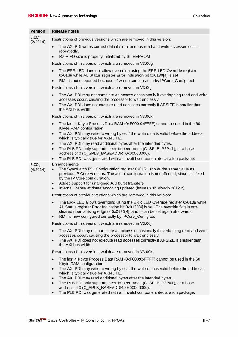
1.7 Release Notes
EtherCAT IP Core updates deliver feature enhancements and removed restrictions. Feature enhancements are not mandatory regarding conformance to the EtherCAT standard. Restrictions have to be judged whether they are relevant in the user’s configuration or not, or if workarounds are possible.
Table 4: Release notes
Version Release notes
3.00c
(5/2013)
Update to ISE 14.3/14.4/14.5, Vivado 2013.1
Removed support for Spartan-3/-3E/-3A/-3AN/-3AN DSP, Virtex-4, and Virtex-5 due to XST incompatibility
Removed OPB support
Removed small/medium/large register sets, added updated preset configurations
Enhancements:
Increased PDI performance
Support for 8/16/32/64 bit AXI4 and AXI4 Lite interface
Support for RGMII ports
Native support for FX PHYs
Support for individual PHY address configuration and reading out this configuration
Support for static or dynamic PHY address configuration
Support for 0 KB Process RAM, DC Sync/Latch signals individually configurable, LED test added
Support for PDI SyncManager/IRQ acknowledge by Write command
Device emulation is now configured in the GUI statically.
MI link detection: relaxed checking of PHY register 9 (1000Base-T Master-Slave Control register)
Restrictions of this version, which are removed in V3.00f:
The AXI PDI may occasionally write incorrect data if simultaneous read and write accesses occur repeatedly.
RX FIFO size is not initialized by SII EEPROM
Restrictions of this version, which are removed in V3.00g:
The ERR LED does not allow overriding using the ERR LED Override register 0x0139 while AL Status register Error Indication bit 0x0130[4] is set
RMII is not supported because of wrong configuration by IPCore_Config tool
Restrictions of this version, which are removed in V3.00j:
The AXI PDI may not complete an access occasionally if overlapping read and write accesses occur, causing the processor to wait endlessly.
The AXI PDI does not execute read accesses correctly if ARSIZE is smaller than the AXI bus width.
Restrictions of this version, which are removed in V3.00k:
The last 4 Kbyte Process Data RAM (0xF000:0xFFFF) cannot be used in the 60 Kbyte RAM configuration.
The AXI PDI may write to wrong bytes if the write data is valid before the address, which is typically true for AXI4LITE.
The AXI PDI may read additional bytes after the intended bytes.
The PLB PDI only supports peer-to-peer mode (C_SPLB_P2P=1), or a base address of 0 (C_SPLB_BASEADDR=0x00000000).
The PLB PDI was generated with an invalid component declaration package.
Overview
Slave Controller – IP Core for Xilinx FPGAs III-7
Version Release notes
3.00f (2/2014)
Restrictions of previous versions which are removed in this version:
The AXI PDI writes correct data if simultaneous read and write accesses occur repeatedly.
RX FIFO size is properly initialized by SII EEPROM
Restrictions of this version, which are removed in V3.00g:
The ERR LED does not allow overriding using the ERR LED Override register 0x0139 while AL Status register Error Indication bit 0x0130[4] is set
RMII is not supported because of wrong configuration by IPCore_Config tool
Restrictions of this version, which are removed in V3.00j:
The AXI PDI may not complete an access occasionally if overlapping read and write accesses occur, causing the processor to wait endlessly.
The AXI PDI does not execute read accesses correctly if ARSIZE is smaller than the AXI bus width.
Restrictions of this version, which are removed in V3.00k:
The last 4 Kbyte Process Data RAM (0xF000:0xFFFF) cannot be used in the 60 Kbyte RAM configuration.
The AXI PDI may write to wrong bytes if the write data is valid before the address, which is typically true for AXI4LITE.
The AXI PDI may read additional bytes after the intended bytes.
The PLB PDI only supports peer-to-peer mode (C_SPLB_P2P=1), or a base address of 0 (C_SPLB_BASEADDR=0x00000000).
The PLB PDI was generated with an invalid component declaration package.
3.00g
(4/2014)
Enhancements:
The Sync/Latch PDI Configuration register 0x0151 shows the same value as previous IP Core versions. The actual configuration is not affected, since it is fixed by the IP Core configuration.
Added support for unaligned AXI burst transfers.
Internal license attribute encoding updated (issues with Vivado 2012.x)
Restrictions of previous versions which are removed in this version:
The ERR LED allows overriding using the ERR LED Override register 0x0139 while AL Status register Error Indication bit 0x0130[4] is set. The override flag is now cleared upon a rising edge of 0x0130[4], and it can be set again afterwards.
RMII is now configured correctly by IPCore_Config tool
Restrictions of this version, which are removed in V3.00j:
The AXI PDI may not complete an access occasionally if overlapping read and write accesses occur, causing the processor to wait endlessly.
The AXI PDI does not execute read accesses correctly if ARSIZE is smaller than the AXI bus width.
Restrictions of this version, which are removed in V3.00k:
The last 4 Kbyte Process Data RAM (0xF000:0xFFFF) cannot be used in the 60 Kbyte RAM configuration.
The AXI PDI may write to wrong bytes if the write data is valid before the address, which is typically true for AXI4LITE.
The AXI PDI may read additional bytes after the intended bytes.
The PLB PDI only supports peer-to-peer mode (C_SPLB_P2P=1), or a base address of 0 (C_SPLB_BASEADDR=0x00000000).
The PLB PDI was generated with an invalid component declaration package.

Overview
III-8 Slave Controller – IP Core for Xilinx FPGAs
Version Release notes
3.00j
(9/2014)
Enhancements:
An example design for the Xilinx Zynq ZC702 development kit using Vivado has been added. A Vivado SDK template for this example design is included
The example designs using ISMNET PHY boards have been extended to support COL and CRS signals, which are required for proper PHY configuration.
The PDI watchdog status 0x0110[1] now shows value ‘1’ (watchdog reloaded) if the PDI watchdog is configured to be not available.
The ESI XML device description does not use special data types anymore.
Restrictions of previous versions which are removed in this version:
The AXI PDI completes accesses if overlapping read and write accesses occur.
The AXI PDI executes read accesses correctly if ARSIZE is smaller than the AXI bus width.
Restrictions of this version, which are removed in V3.00k:
The last 4 Kbyte Process Data RAM (0xF000:0xFFFF) cannot be used in the 60 Kbyte RAM configuration.
The AXI PDI may write to wrong bytes if the write data is valid before the address, which is typically true for AXI4LITE.
The AXI PDI may read additional bytes after the intended bytes.
The PLB PDI only supports peer-to-peer mode (C_SPLB_P2P=1), or a base address of 0 (C_SPLB_BASEADDR=0x00000000).
The PLB PDI was generated with an invalid component declaration package.
3.00k
(1/2015) The PlanAhead-based Xilinx Zynq ZC702 example design has been removed, because a Vivado based example design is available.
Enhancements:
For EEPROM Emulation, the CRC error bit 0x0502[11] can be written via PDI to indicate CRC errors during a reload command.
The IPCore_Config tool optionally generates AXI/PLB configurations without the XPS pcores folder structure (e.g. for Vivado).
The AXI4LITE PDI wrapper does no longer contain the unused REGION and QOS signals.
Restrictions of previous versions which are removed in this version:
The last 4 Kbyte Process Data RAM (0xF000:0xFFFF) can be used in the 60 Kbyte RAM configuration.
The AXI PDI does not write to wrong bytes if the write data is valid before the address.
The AXI PDI does not read additional bytes after the intended bytes.
The PLB PDI supports any base address.
The PLB PDI is generated with a valid component declaration package.
Overview
Slave Controller – IP Core for Xilinx FPGAs III-9
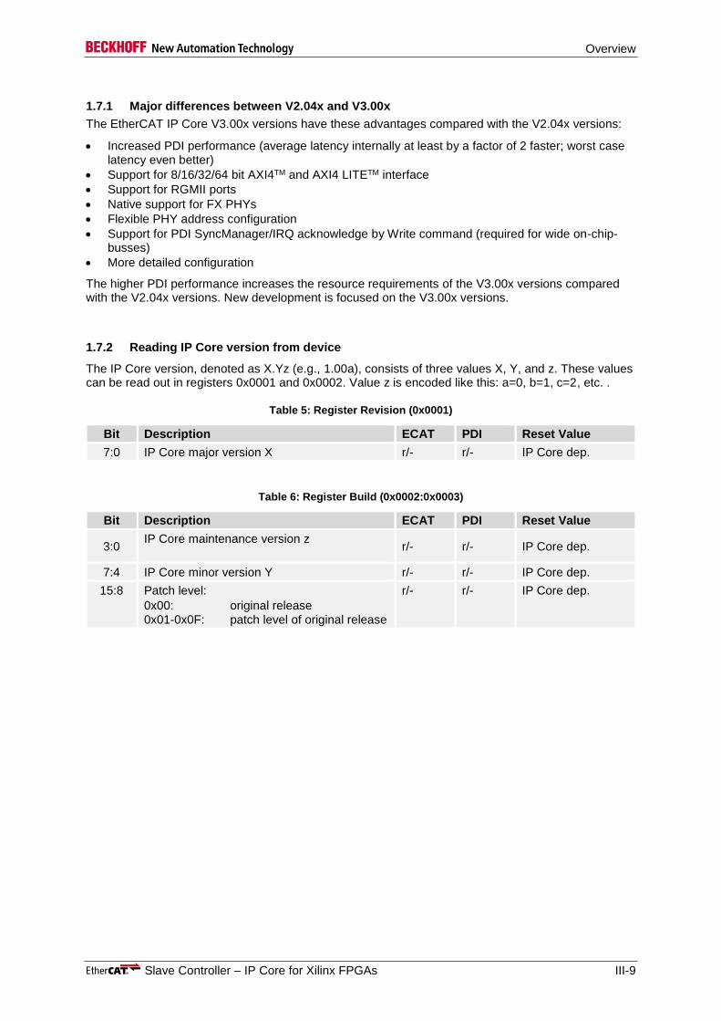
1.7.1 Major differences between V2.04x and V3.00x
The EtherCAT IP Core V3.00x versions have these advantages compared with the V2.04x versions:
Increased PDI performance (average latency internally at least by a factor of 2 faster; worst case latency even better)
Support for 8/16/32/64 bit AXI4TM and AXI4 LITETM interface
Support for RGMII ports
Native support for FX PHYs
Flexible PHY address configuration
Support for PDI SyncManager/IRQ acknowledge by Write command (required for wide on-chip-busses)
More detailed configuration
The higher PDI performance increases the resource requirements of the V3.00x versions compared with the V2.04x versions. New development is focused on the V3.00x versions.
1.7.2 Reading IP Core version from device
The IP Core version, denoted as X.Yz (e.g., 1.00a), consists of three values X, Y, and z. These values can be read out in registers 0x0001 and 0x0002. Value z is encoded like this: a=0, b=1, c=2, etc. .
Table 5: Register Revision (0x0001)
Bit Description ECAT PDI Reset Value
7:0 IP Core major version X r/- r/- IP Core dep.
Table 6: Register Build (0x0002:0x0003)
Bit Description ECAT PDI Reset Value
3:0 IP Core maintenance version z
r/- r/- IP Core dep.
7:4 IP Core minor version Y r/- r/- IP Core dep.
15:8 Patch level:
0x00: original release 0x01-0x0F: patch level of original release
r/- r/- IP Core dep.
Overview
III-10 Slave Controller – IP Core for Xilinx FPGAs
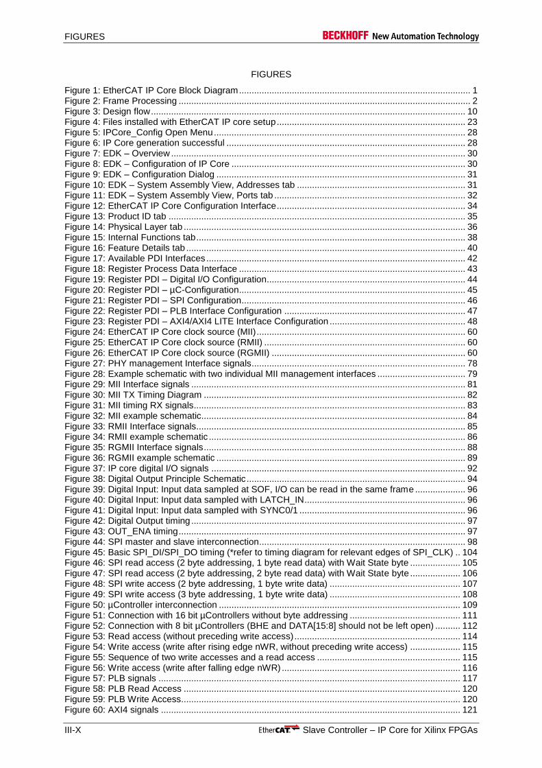
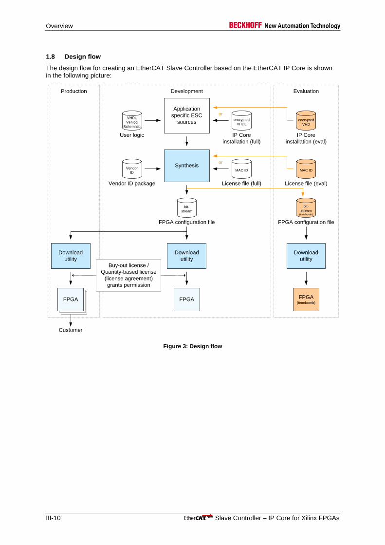
1.8 Design flow
The design flow for creating an EtherCAT Slave Controller based on the EtherCAT IP Core is shown in the following picture:
IP Core
installation (eval)
Synthesis
User logic
Vendor ID package License file (full)
FPGA configuration file
Download
utility
FPGA
Buy-out license /
Quantity-based license
(license agreement)
grants permission
EvaluationDevelopment
Download
utility
MAC IDVendor
ID
bit-
stream
Application
specific ESC
sourcesVHDL
Verilog
Schematic
Production
FPGAFPGA
Download
utility
FPGA
encrypted
VHD
FPGA configuration file
bit-
stream(timebomb)
FPGA(timebomb)
IP Core
installation (full)
encrypted
VHDL
or
Customer
License file (eval)
MAC ID
or
Figure 3: Design flow

Overview
Slave Controller – IP Core for Xilinx FPGAs III-11
1.9 IP Core Evaluation
The EtherCAT IP Core for Xilinx FPGAs supports IP core evaluation. A dedicated setup file containing the evaluation version of the IP Core is available, which also includes the decryption keys for the evaluation IP Core. Additionally, a special evaluation license file is required for IP core evaluation.
A design with the evaluation version of the EtherCAT IP Core is subject to some restrictions:
The EtherCAT IP Core will discontinue its function after approximately one hour.
The evaluation version slightly increases the resource consumption of the IP Core.
The evaluation bitstream must not be distributed/sold.
A vendor ID package is required for both evaluation and full license. It is recommended to use an evaluation vendor ID (package) for evaluation, and the original vendor ID for production. The evaluation vendor ID is beginning with “0xE.......” and ends with the original vendor ID digits. Evaluation vendor IDs cannot pass the EtherCAT conformance tests.
Selecting Full or Evaluation License
There are individual setup files for full and evaluation license. The evaluation version can be easily upgraded to a full version just by running the EtherCAT IP Core setup for the full version.
For Linux, just install the full version over the evaluation license, the appropriate files will be overwritten.
A design using an evaluation EtherCAT IP Core does not have to be changed when upgrading to a full license (or vice-versa).
Four steps have to be performed to change the license type:
1. Acquire the intended license and set it up 2. Windows:
Start the appropriate EtherCAT IP Core setup. Alternatively, uninstall the EtherCAT IP Core and install it again with the intended license version. The example designs are automatically updated and the decryption keys are also installed. Linux: Unzip the setup files over the existing installation (you might want to delete the installation folder <IPInst_dir> before). Copy the new decryption keys from the <IPInst_dir>/lib folder to your $HOME/RSA folder.
3. Update your own projects with the EtherCAT_IPCore.vhd from the lib-folder. For EDK projects, it is sufficient to generate the core again, because the IPCore_Config tool will integrate the current IP Core from the lib folder.
4. Synthesize your designs again to generate unlimited bitstreams with the full license, and time-bombed bitstreams with the evaluation license.
A txt-file is placed in the lib folder which indicates the currently installed IP core version (evaluation or full).
Overview
III-12 Slave Controller – IP Core for Xilinx FPGAs
1.10 Simulation
A behavioral simulation model of the EtherCAT IP core is not available because of its size and complexity. Thus, simulation of the entire EtherCAT IP Core is not supported. In most cases, simulation of the EtherCAT IP Core is not necessary, as the IP Core was thoroughly tested and the interfaces are standardized (Ethernet, PLB, AXI) or simple and well described. Problems at the interface level can often be solved with a scope shot of the interface signals.
Nevertheless, customer designs using the PLB or AXI on-chip bus can easily be simulated using a Bus Functional Model of the on-chip bus slave interface instead of a simulation model of the entire EtherCAT IP Core.
From the processor’s view, the EtherCAT IP Core is a memory (or a bunch of registers). For processor bus verification, the EtherCAT IP Core can be substituted by another IP core with PLB/AXI slave interface which behaves like a memory as well. The EtherCAT IP Core can be replaced for simulation by e.g.:
Xilinx XPS Block RAM (BRAM) Interface Controller with a Block RAM block
PLB Bus Functional models of the “IBM On-Chip Bus Model Toolkits”. This toolkit can be used for complete verification of your PLB bus interfaces.
AXI slave Bus Functional models
Features and Registers
Slave Controller – IP Core for Xilinx FPGAs III-13
2 Features and Registers
2.1 Features
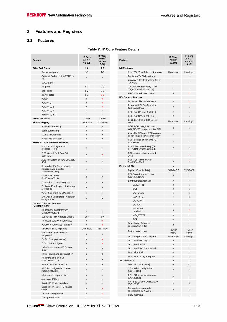
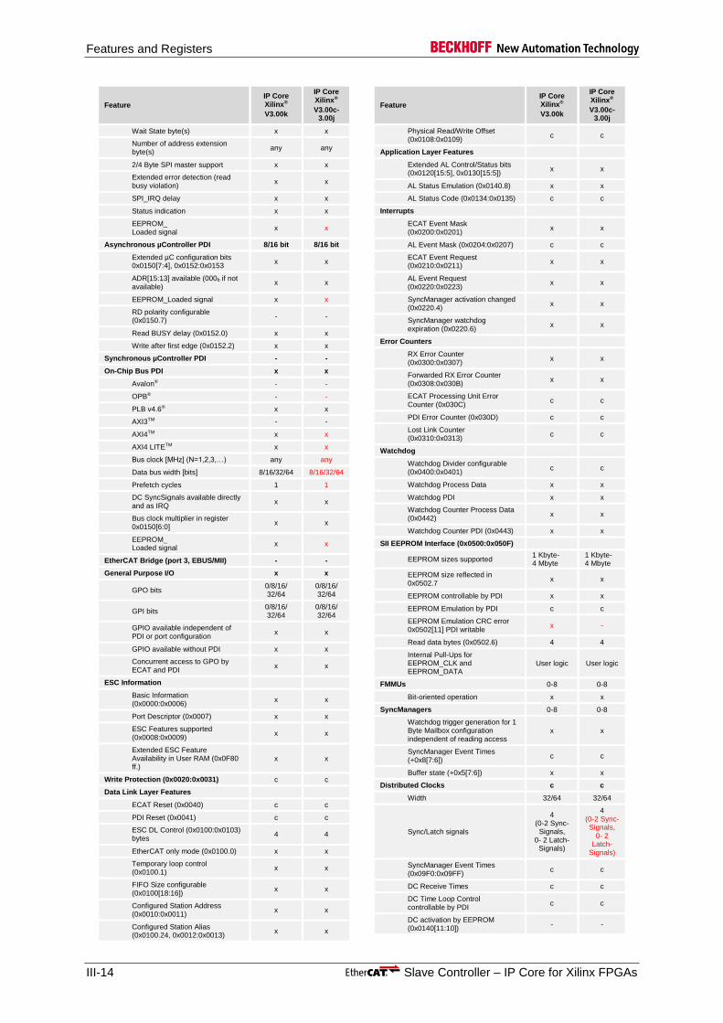
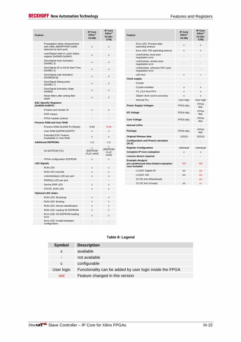
Table 7: IP Core Feature Details
Feature
IP Core Xilinx®
V3.00k
IP Core Xilinx®
V3.00c-3.00j
EtherCAT Ports 1-3 1-3
Permanent ports 1-3 1-3
Optional Bridge port 3 (EBUS or MII)
- -
EBUS ports - -
MII ports 0-3 0-3
RMII ports 0-2 0-2
RGMII ports 0-3 0-3
Port 0 x x
Ports 0, 1 x x
Ports 0, 1, 2 x x
Ports 0, 1, 3 - -
Ports 0, 1, 2, 3 - -
EtherCAT mode Direct Direct
Slave Category Full Slave Full Slave
Position addressing x x
Node addressing x x
Logical addressing x x
Broadcast addressing x x
Physical Layer General Features
FIFO Size configurable (0x0100[18:16])
x x
FIFO Size default from SII EEPROM
x x
Auto-Forwarder checks CRC and SOF
x x
Forwarded RX Error indication, detection and Counter (0x0308:0x030B)
x x
Lost Link Counter (0x0310:0x0313)
c c
Prevention of circulating frames x x
Fallback: Port 0 opens if all ports are closed
x x
VLAN Tag and IP/UDP support x x
Enhanced Link Detection per port configurable
x x
General Ethernet Features (MII/RMII/RGMII)
MII Management Interface (0x0510:0x051F)
c c
Supported PHY Address Offsets any any
Individual port PHY addresses x x
Port PHY addresses readable x x
Link Polarity configurable User logic User logic
Enhanced Link Detection supported
x x
FX PHY support (native) x x
PHY reset out signals x x
Link detection using PHY signal (LED)
x x
MI link status and configuration c c
MI controllable by PDI (0x0516:0x0517)
x x
MI read error (0x0510.13) x x
MI PHY configuration update status (0x0518.5)
x x
MI preamble suppression x x
Additional MCLK x x
Gigabit PHY configuration x x
Gigabit PHY register 9 relaxed check
x x
FX PHY configuration x x
Transparent Mode - -
Feature
IP Core Xilinx®
V3.00k
IP Core Xilinx®
V3.00c-3.00j
MII Features
CLK25OUT as PHY clock source User logic User logic
Bootstrap TX Shift settings c c
Automatic TX Shift setting (with TX_CLK)
c c
TX Shift not necessary (PHY TX_CLK as clock source)
- -
FIFO size reduction steps 2 2
PDI General Features
Increased PDI performance x x
Extended PDI Configuration (0x0152:0x0153)
x x
PDI Error Counter (0x030D) c c
PDI Error Code (0x030E) c c
CPU_CLK output (10, 20, 25 MHz)
User logic User logic
SOF, EOF, WD_TRIG and WD_STATE independent of PDI
x x
Available PDIs and PDI features depending on port configuration
- -
PDI selection at run-time (SII EEPROM)
- -
PDI active immediately (SII EEPROM settings ignored)
x x
PDI function acknowledge by write
c c
PDI Information register 0x014E:0x014F
c c
Digital I/O PDI x x
Digital I/O width [bits] 8/16/24/32 8/16/24/32
PDI Control register value (0x0140:0x0141)
4 4
Control/Status signals: 7 7
LATCH_IN x x
SOF x x
OUTVALID x x
WD_TRIG x x
OE_CONF - -
OE_EXT x x
EEPROM_ Loaded
x x
WD_STATE x x
EOF x x
Granularity of direction configuration [bits]
8 8
Bidirectional mode - (User logic)
- (User logic)
Output high-Z if WD expired User logic User logic
Output 0 if WD expired x x
Output with EOF x x
Output with DC SyncSignals x x
Input with SOF x x
Input with DC SyncSignals x x
SPI Slave PDI x x
Max. SPI clock [MHz] 30 30
SPI modes configurable (0x0150[1:0])
x x
SPI_IRQ driver configurable (0x0150[3:2])
x x
SPI_SEL polarity configurable (0x0150.4)
x x
Data out sample mode configurable (0x0150.5)
x x
Busy signaling - -
Features and Registers
III-14 Slave Controller – IP Core for Xilinx FPGAs
Feature
IP Core Xilinx®
V3.00k
IP Core Xilinx®
V3.00c-3.00j
Wait State byte(s) x x
Number of address extension byte(s)
any any
2/4 Byte SPI master support x x
Extended error detection (read busy violation)
x x
SPI_IRQ delay x x
Status indication x x
EEPROM_ Loaded signal
x x
Asynchronous µController PDI 8/16 bit 8/16 bit
Extended µC configuration bits 0x0150[7:4], 0x0152:0x0153
x x
ADR[15:13] available (000b if not available)
x x
EEPROM_Loaded signal x x
RD polarity configurable (0x0150.7)
- -
Read BUSY delay (0x0152.0) x x
Write after first edge (0x0152.2) x x
Synchronous µController PDI - -
On-Chip Bus PDI x x
Avalon® - -
OPB® - -
PLB v4.6® x x
AXI3TM - -
AXI4TM x x
AXI4 LITETM x x
Bus clock [MHz] (N=1,2,3,…) any any
Data bus width [bits] 8/16/32/64 8/16/32/64
Prefetch cycles 1 1
DC SyncSignals available directly and as IRQ
x x
Bus clock multiplier in register 0x0150[6:0]
x x
EEPROM_ Loaded signal
x x
EtherCAT Bridge (port 3, EBUS/MII) - -
General Purpose I/O x x
GPO bits 0/8/16/ 32/64
0/8/16/ 32/64
GPI bits 0/8/16/ 32/64
0/8/16/ 32/64
GPIO available independent of PDI or port configuration
x x
GPIO available without PDI x x
Concurrent access to GPO by ECAT and PDI
x x
ESC Information
Basic Information (0x0000:0x0006)
x x
Port Descriptor (0x0007) x x
ESC Features supported (0x0008:0x0009)
x x
Extended ESC Feature Availability in User RAM (0x0F80 ff.)
x x
Write Protection (0x0020:0x0031) c c
Data Link Layer Features
ECAT Reset (0x0040) c c
PDI Reset (0x0041) c c
ESC DL Control (0x0100:0x0103) bytes
4 4
EtherCAT only mode (0x0100.0) x x
Temporary loop control (0x0100.1)
x x
FIFO Size configurable (0x0100[18:16])
x x
Configured Station Address (0x0010:0x0011)
x x
Configured Station Alias (0x0100.24, 0x0012:0x0013)
x x
Feature
IP Core Xilinx®
V3.00k
IP Core Xilinx®
V3.00c-3.00j
Physical Read/Write Offset (0x0108:0x0109)
c c
Application Layer Features
Extended AL Control/Status bits (0x0120[15:5], 0x0130[15:5])
x x
AL Status Emulation (0x0140.8) x x
AL Status Code (0x0134:0x0135) c c
Interrupts
ECAT Event Mask (0x0200:0x0201)
x x
AL Event Mask (0x0204:0x0207) c c
ECAT Event Request (0x0210:0x0211)
x x
AL Event Request (0x0220:0x0223)
x x
SyncManager activation changed (0x0220.4)
x x
SyncManager watchdog expiration (0x0220.6)
x x
Error Counters
RX Error Counter (0x0300:0x0307)
x x
Forwarded RX Error Counter (0x0308:0x030B)
x x
ECAT Processing Unit Error Counter (0x030C)
c c
PDI Error Counter (0x030D) c c
Lost Link Counter (0x0310:0x0313)
c c
Watchdog
Watchdog Divider configurable (0x0400:0x0401)
c c
Watchdog Process Data x x
Watchdog PDI x x
Watchdog Counter Process Data (0x0442)
x x
Watchdog Counter PDI (0x0443) x x
SII EEPROM Interface (0x0500:0x050F)
EEPROM sizes supported 1 Kbyte-4 Mbyte
1 Kbyte-4 Mbyte
EEPROM size reflected in 0x0502.7
x x
EEPROM controllable by PDI x x
EEPROM Emulation by PDI c c
EEPROM Emulation CRC error 0x0502[11] PDI writable
x -
Read data bytes (0x0502.6) 4 4
Internal Pull-Ups for EEPROM_CLK and EEPROM_DATA
User logic User logic
FMMUs 0-8 0-8
Bit-oriented operation x x
SyncManagers 0-8 0-8
Watchdog trigger generation for 1 Byte Mailbox configuration independent of reading access
x x
SyncManager Event Times (+0x8[7:6])
c c
Buffer state (+0x5[7:6]) x x
Distributed Clocks c c
Width 32/64 32/64
Sync/Latch signals
4 (0-2 Sync-Signals,
0- 2 Latch-Signals)
4 (0-2 Sync-Signals,
0- 2 Latch-
Signals)
SyncManager Event Times (0x09F0:0x09FF)
c c
DC Receive Times c c
DC Time Loop Control controllable by PDI
c c
DC activation by EEPROM (0x0140[11:10])
- -
Features and Registers
Slave Controller – IP Core for Xilinx FPGAs III-15
Feature
IP Core Xilinx®
V3.00k
IP Core Xilinx®
V3.00c-3.00j
Propagation delay measurement with traffic (BWR/FPWR 0x900 detected at each port)
x x
LatchSignal state in Latch Status register (0x09AE:0x09AF)
x x
SyncSignal Auto-Activation (0x0981.3)
x x
SyncSignal 32 or 64 bit Start Time (0x0981.4)
x x
SyncSignal Late Activation (0x0981[6:5])
x x
SyncSignal debug pulse (0x0981.7)
x x
SyncSignal Activation State 0x0984)
x x
Reset filters after writing filter depth
x x
ESC Specific Registers (0x0E00:0x0EFF)
Product and Vendor ID x x
POR Values - -
FPGA Update (online) - -
Process RAM and User RAM
Process RAM (0x1000 ff.) [Kbyte] 0-60 0-60
User RAM (0x0F80:0x0FFF) x x
Extended ESC Feature Availability in User RAM
x x
Additional EEPROMs 1-2 1-2
SII EEPROM (I²C)
c (EEPROM
of µC used)
c (EEPROM
of µC used)
FPGA configuration EEPROM x x
LED Signals
RUN LED c c
RUN LED override c c
Link/Activity(x) LED per port x x
PERR(x) LED per port - -
Device ERR LED c c
STATE_RUN LED c c
Optional LED states
RUN LED: Bootstrap x x
RUN LED: Booting c c
RUN LED: Device identification c c
RUN LED: loading SII EEPROM c c
Error LED: SII EEPROM loading error
c c
Error LED: Invalid hardware configuration
- -
Feature
IP Core Xilinx®
V3.00k
IP Core Xilinx®
V3.00c-3.00j
Error LED: Process data watchdog timeout
c c
Error LED: PDI watchdog timeout c c
Link/Activity: local auto-negotiation error
- -
Link/Activity: remote auto-negotiation error
- -
Link/Activity: unknown PHY auto-negotiation error
- -
LED test c c
Clock supply
Crystal - -
Crystal oscillator x x
TX_CLK from PHY x x
25ppm clock source accuracy x x
Internal PLL User logic User logic
Power Supply Voltages FPGA dep. FPGA dep.
I/O Voltage FPGA dep. FPGA dep.
Core Voltage FPGA dep. FPGA dep.
Internal LDOs - -
Package FPGA dep. FPGA dep.
Original Release date 1/2015 5/2013
Configuration and Pinout calculator (XLS)
- -
Register Configuration individual individual
Complete IP Core evaluation x x
License device required - -
Example designs/
pre-synthesized time-limited evaluation core included
3/3 4/3
LX150T Digital I/O x/x x/x
LX150T AXI x/x x/x
ZC702 AXI (PlanAhead) - x/x
ZC702 AXI (Vivado) x/x x/-
Table 8: Legend
Symbol Description
x available
- not available
c configurable
User logic Functionality can be added by user logic inside the FPGA
red Feature changed in this version

Features and Registers
III-16 Slave Controller – IP Core for Xilinx FPGAs
2.2 Registers
An EtherCAT Slave Controller (ESC) has an address space of 64KByte. The first block of 4KByte (0x0000:0x0FFF) is dedicated for registers. The process data RAM starts at address 0x1000, its size is configurable.
Some registers are implemented depending on the configuration.
Table 9 gives an overview of the available registers.
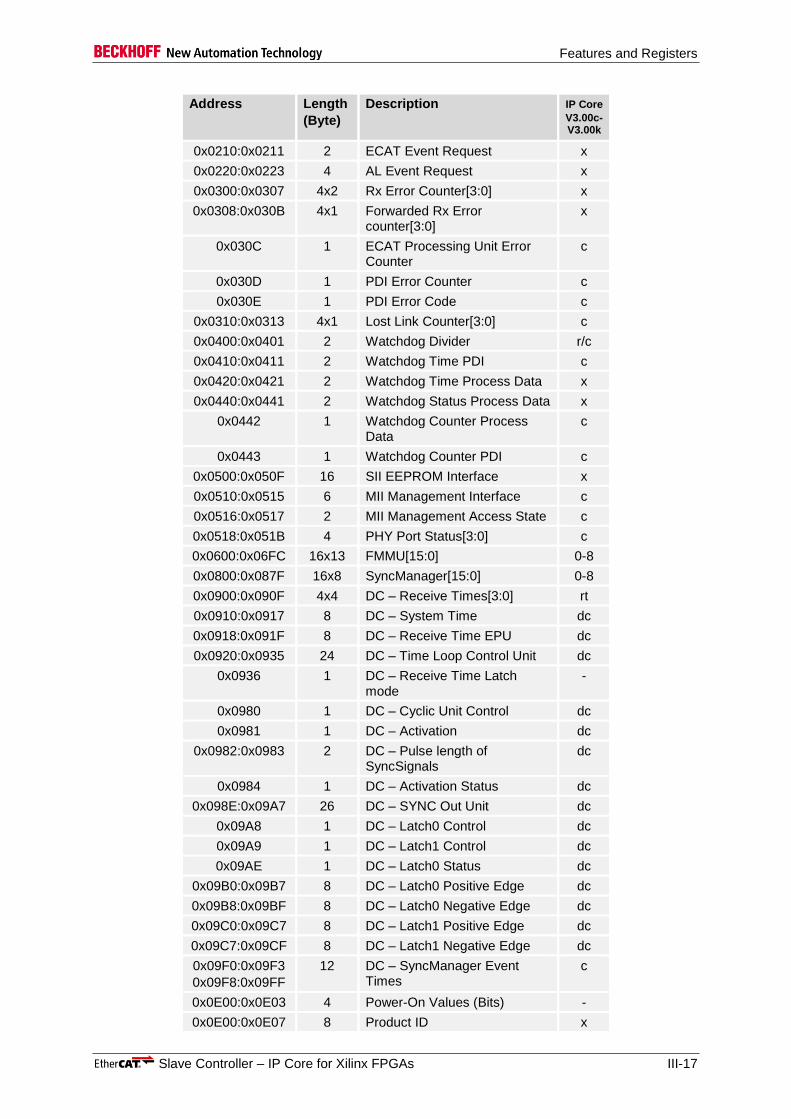
Table 9: Register availability
Address Length
(Byte)
Description IP Core
V3.00c-V3.00k
0x0000 1 Type x
0x0001 1 Revision x
0x0002:0x0003 2 Build x
0x0004 1 FMMUs supported x
0x0005 1 SyncManagers supported x
0x0006 1 RAM Size x
0x0007 1 Port Descriptor x
0x0008:0x0009 2 ESC Features supported x
0x0010:0x0011 2 Configured Station Address x
0x0012:0x0013 2 Configured Station Alias x
0x0020 1 Write Register Enable c
0x0021 1 Write Register Protection c
0x0030 1 ESC Write Enable c
0x0031 1 ESC Write Protection c
0x0040 1 ESC Reset ECAT c
0x0041 1 ESC Reset PDI c
0x0100:0x0101 2 ESC DL Control x
0x0102:0x0103 2 Extended ESC DL Control x
0x0108:0x0109 2 Physical Read/Write Offset c
0x0110:0x0111 2 ESC DL Status x
0x0120 5 bits [4:0]
AL Control x
0x0120:0x0121 2 AL Control x
0x0130 5 bits [4:0]
AL Status x
0x0130:0x0131 2 AL Status x
0x0134:0x0135 2 AL Status Code c
0x0138 1 RUN LED Override c
0x0139 1 ERR LED Override c
0x0140 1 PDI Control x
0x0141 1 ESC Configuration x
0x014E:0x014F 2 PDI Information c
0x0150 1 PDI Configuration x
0x0151 1 DC Sync/Latch Configuration x
0x0152:0x0153 2 Extended PDI Configuration x
0x0200:0x0201 2 ECAT Event Mask x
0x0204:0x0207 4 PDI0 AL Event Mask r/c
Features and Registers
Slave Controller – IP Core for Xilinx FPGAs III-17
Address Length
(Byte)
Description IP Core
V3.00c-V3.00k
0x0210:0x0211 2 ECAT Event Request x
0x0220:0x0223 4 AL Event Request x
0x0300:0x0307 4x2 Rx Error Counter[3:0] x
0x0308:0x030B 4x1 Forwarded Rx Error counter[3:0]
x
0x030C 1 ECAT Processing Unit Error Counter
c
0x030D 1 PDI Error Counter c
0x030E 1 PDI Error Code c
0x0310:0x0313 4x1 Lost Link Counter[3:0] c
0x0400:0x0401 2 Watchdog Divider r/c
0x0410:0x0411 2 Watchdog Time PDI c
0x0420:0x0421 2 Watchdog Time Process Data x
0x0440:0x0441 2 Watchdog Status Process Data x
0x0442 1 Watchdog Counter Process Data
c
0x0443 1 Watchdog Counter PDI c
0x0500:0x050F 16 SII EEPROM Interface x
0x0510:0x0515 6 MII Management Interface c
0x0516:0x0517 2 MII Management Access State c
0x0518:0x051B 4 PHY Port Status[3:0] c
0x0600:0x06FC 16x13 FMMU[15:0] 0-8
0x0800:0x087F 16x8 SyncManager[15:0] 0-8
0x0900:0x090F 4x4 DC – Receive Times[3:0] rt
0x0910:0x0917 8 DC – System Time dc
0x0918:0x091F 8 DC – Receive Time EPU dc
0x0920:0x0935 24 DC – Time Loop Control Unit dc
0x0936 1 DC – Receive Time Latch mode
-
0x0980 1 DC – Cyclic Unit Control dc
0x0981 1 DC – Activation dc
0x0982:0x0983 2 DC – Pulse length of SyncSignals
dc
0x0984 1 DC – Activation Status dc
0x098E:0x09A7 26 DC – SYNC Out Unit dc
0x09A8 1 DC – Latch0 Control dc
0x09A9 1 DC – Latch1 Control dc
0x09AE 1 DC – Latch0 Status dc
0x09B0:0x09B7 8 DC – Latch0 Positive Edge dc
0x09B8:0x09BF 8 DC – Latch0 Negative Edge dc
0x09C0:0x09C7 8 DC – Latch1 Positive Edge dc
0x09C7:0x09CF 8 DC – Latch1 Negative Edge dc
0x09F0:0x09F3
0x09F8:0x09FF
12 DC – SyncManager Event Times
c
0x0E00:0x0E03 4 Power-On Values (Bits) -
0x0E00:0x0E07 8 Product ID x

Features and Registers
III-18 Slave Controller – IP Core for Xilinx FPGAs
Address Length
(Byte)
Description IP Core
V3.00c-V3.00k
0x0E08:0x0E0F 8 Vendor ID x
0x0F00:0x0F03 4 Digital I/O Output Data io
0x0F10:0x0F17 8 General Purpose Outputs [Byte]
0-8
0x0F18:0x0F1F 8 General Purpose Inputs [Byte] 0-8
0x0F80:0x0FFF 128 User RAM x
0x1000:0x1003 4 Digital I/O Input Data io
0x1000 ff. Process Data RAM [Kbyte] 1-60
Table 10: Legend
Symbol Description
x Available
- Not available
r Read only
c Configurable
dc Available if Distributed Clocks with all Sync/Latch signals are enabled
rt Available if Receive Times or Distributed Clocks are enabled (always available for 3-4 ports)
io Available if Digital I/O PDI is selected
red Register changed in this version

Features and Registers
Slave Controller – IP Core for Xilinx FPGAs III-19
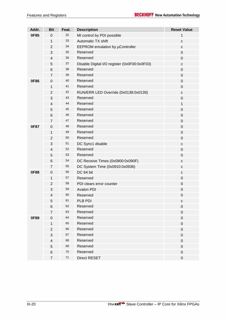
2.3 Extended ESC Features in User RAM
Table 11: Extended ESC Features (Reset values of User RAM – 0x0F80:0x0FFF)
Addr. Bit Feat. Description Reset Value
0F80 7:0 - Number of extended feature bits Depends on ESC
IP Core extended features:
Depends on ESC:
0: Not available
1: Available
c: Configurable
0F81 0 0 Extended DL Control Register (0x0102:0x0103) 1
1 1 AL Status Code Register (0x0134:0x0135) c
2 2 ECAT Interrupt Mask (0x0200:0x0201) 1
3 3 Configured Station Alias (0x0012:0x0013) 1
4 4 General Purpose Inputs (0x0F18:0x0F1F) c
5 5 General Purpose Outputs (0x0F10:0x0F17) c
6 6 AL Event Mask (0x0204:0x0207) c
7 7 Physical Read/Write Offset (0x0108:0x0109) c
0F82 0 8 Watchdog divider writeable (0x0400:0x04001) and Watchdog PDI (0x0410:0x0f11)
c
1 9 Watchdog counters (0x0442:0x0443) c
2 10 Write Protection (0x0020:0x0031) c
3 11 Reset (0x0040:0x0041) c
4 12 Reserved 0
5 13 DC SyncManager Event Times (0x09F0:0x09FF) c
6 14 ECAT Processing Unit/PDI Error Counter (0x030C:0x030D)
c
7 15 EEPROM Size configurable (0x0502.7):
0: EEPROM Size fixed to sizes up to 16 Kbit
1: EEPROM Size configurable
1
0F83 0 16 Reserved 1
1 17 Reserved 0
2 18 Reserved 0
3 19 Lost Link Counter (0x0310:0x0313) c
4 20 MII Management Interface (0x0510:0x0515) c
5 21 Enhanced Link Detection MII c
6 22 Enhanced Link Detection EBUS 0
7 23 Run LED (DEV_STATE LED) c
0F84 0 24 Link/Activity LED 1
1 25 Reserved 0
2 26 Reserved 1
3 27 DC Latch In Unit c
4 28 Reserved 0
5 29 DC Sync Out Unit c
6 30 DC Time loop control assigned to PDI c
7 31 Link detection and configuration by MI c
Features and Registers
III-20 Slave Controller – IP Core for Xilinx FPGAs
Addr. Bit Feat. Description Reset Value
0F85 0 32 MI control by PDI possible 1
1 33 Automatic TX shift c
2 34 EEPROM emulation by µController c
3 35 Reserved 0
4 36 Reserved 0
5 37 Disable Digital I/O register (0x0F00:0x0F03) c
6 38 Reserved 0
7 39 Reserved 0
0F86 0 40 Reserved 0
1 41 Reserved 0
2 42 RUN/ERR LED Override (0x0138:0x0139) c
3 43 Reserved 0
4 44 Reserved 1
5 45 Reserved 0
6 46 Reserved 0
7 47 Reserved 0
0F87 0 48 Reserved 0
1 49 Reserved 0
2 50 Reserved 0
3 51 DC Sync1 disable c
4 52 Reserved 0
5 53 Reserved 0
6 54 DC Receive Times (0x0900:0x090F) c
7 55 DC System Time (0x0910:0x0936) c
0F88 0 56 DC 64 bit c
1 57 Reserved 0
2 58 PDI clears error counter 0
3 59 Avalon PDI 0
4 60 Reserved 0
5 61 PLB PDI c
6 62 Reserved 0
7 63 Reserved 0
0F89 0 64 Reserved 0
1 65 Reserved 0
2 66 Reserved 0
3 67 Reserved 0
4 68 Reserved 0
5 69 Reserved 0
6 70 Reserved 0
7 71 Direct RESET 0

Features and Registers
Slave Controller – IP Core for Xilinx FPGAs III-21
Addr. Bit Feat. Description Reset Value
0F8A 0 72 Reserved 0
1 73 Reserved 1
2 74 DC Latch1 disable c
3 75 AXI PDI c
4 76 Reserved 0
5 77 Reserved 0
6 78 PDI function acknowledge by PDI write c
7 79 Reserved 0
0F8B 0 80 Reserved 1
1 81 Reserved 1
2 82 Reserved 0
3 83 LED test c
4 84 Reserved 0
5 85 Reserved 0
6 86 Reserved 0
7 87 Reserved 0
0F8C 3:0 91:88 Reserved 0
7:4 95:92 Reserved 0
0F8D 3:0 99:96 Reserved 0
7:4 103:100 Reserved 0
0F8E 3:0 107:104 Reserved 0
4 108 Reserved 0
5 109 Reserved 0
7:6 111:110 Digital I/O PDI byte size c
0F8F 0 112 Reserved 0
1 113 Reserved 0
2 114 Digital I/O PDI c
3 115 SPI PDI c
4 116 Asynchronous µC PDI c
5 117 Reserved 0
6 118 Reserved 1
7 119 Reserved 1
0F90 0 120 Reserved 0
1 121 Reserved 0
2 122 Reserved 0
3 123 Reserved 0
4 124 Reserved 0
5 125 Reserved 0
6 126 Reserved 0
7 127 Reserved 0

Features and Registers
III-22 Slave Controller – IP Core for Xilinx FPGAs
Addr. Bit Feat. Description Reset Value
0F91 0 128 Reserved 0
1 129 Reserved 0
2 130 Reserved 0
3 131 Reserved 0
4 132 Reserved 0
5 133 Reserved 0
6 134 Reserved 0
7 135 Reserved 0
0F92 0 136 Reserved 0
1 137 Reserved 0
2 138 Reserved 0
3 139 Reserved 0
4 140 Reserved 0
5 141 Reserved 0
6 142 Reserved 0
7 143 Reserved 0
0F93 0 144 RGMII c
1 145 Individual PHY address read out (0x0510[7:3]) c
2 146 CLK_PDI_EXT is asynchronous c
3 147 Reserved 0
4 148 Use RGMII GTX_CLK phase shifted clock input 1
5 149 RMII c
6 150 Reserved 0
7 151 Reserved 0

IP Core Installation
Slave Controller – IP Core for Xilinx FPGAs III-23
3 IP Core Installation
3.1 Installation on Windows PCs
3.1.1 System Requirements
The system requirements of the Xilinx Design tools are applicable. The EtherCAT IP Core configuration tool has these additional requirements:
Microsoft .NET Framework 2.0 (available from Microsoft, http://www.microsoft.com)
3.1.2 Installation
For installation of the EtherCAT IP Core on your system run the setup program
“EtherCAT IP core for Xilinx FPGAs <version> Setup.exe”
and follow the instructions of the installation wizard.
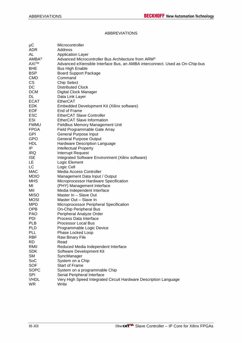
The EtherCAT IP Core and documentation are typically installed in the directory
C:\BECKHOFF\ethercat_<version>
This folder is further referenced to as <IPInst_dir>.
Figure 4: Files installed with EtherCAT IP core setup
IP Core Library and decryption keys
Example designs
XML Device Description for Example Designs
Installation directory <IPInst_dir>
Documentation
Configuration Tool
Software templates for EDK
Software templates for Vivado
IP Core Installation
III-24 Slave Controller – IP Core for Xilinx FPGAs
3.2 Installation on Linux PCs
3.2.1 System Requirements
The system requirements of the Xilinx Design tools are applicable. The EtherCAT IP Core configuration tool has these additional requirements1:
Mono 1.2.6 or higher (software for running Microsoft .NET Framework programs, available at http://www.mono-project.com)
3.2.2 Installation
For installation of the EtherCAT IP Core extract the archive to any folder on your Linux PC (same contents as on windows PCs):
1. Create installation directory, , e.g. /opt/beckkhoff/ : # mkdir /opt/beckhoff
2. Change to installation directory # cd /opt/beckhoff
3. Copy EtherCAT IP Core archive to installation folder 4. Extract the EtherCAT IP Core:
# tar –xf EtherCAT_IP_core_for_Xilinx_FPGAs_<version>_Linux_
<region>.tar.gz
5. Continue with the following installation chapters.
The folder
ethercat_<version>
created inside this directory is further referenced to as <IPInst_dir>.
3.3 Files located in the lib folder
Table 12: Contents of lib folder
File name Description
EtherCAT_CLK.vhd Example EtherCAT clock supply
EtherCAT_IPCore.vhd Encrypted EtherCAT IP Core source code
EtherCAT_Reset.vhd Example EtherCAT reset supply
pk_ECAT_VENDORID_<company>_Xilinx_RSA.vhd Vendor ID package (added during installation, not part of setup)
rsa_ethercat_base_pvt.pem RSA decryption key for Vendor ID package
rsa_ethercat_ip_<version>_<type>_pvt.pem RSA decryption key for EtherCAT IP Core
The full version of EtherCAT_IPCore.vhd was installed.txt
or
The evaluation version of EtherCAT_IPCore.vhd was installed.txt
Name of this empty text file indicates which version of EtherCAT_IPCore.vhd is present in this folder
1 Not all of these variants have been tested with the EtherCAT IP core.
IP Core Installation
Slave Controller – IP Core for Xilinx FPGAs III-25
3.4 License File
The license file for the EtherCAT IP Core (iptb_ethercat_ipcore_<version>_flexlm.lic) has to be made available to the Xilinx tools. The EtherCAT IP Core can only be used with a license file.
There are two options:
1. In Xilinx ISE select “Help – Manage License…” from the menu, and press the “Copy License…” button in the Manage Xilinx Licenses tab. Select the license file you have received from Beckhoff. This will copy the license file to C:\.Xilinx\ on Windows PCs (please note the dot before Xilinx\), or <HOME directory>/.Xilinx/ on Linux PCs
2. Add the path of the license file to the LM_LICENSE_FILE environment variable (separated by a semicolon). This variable can also be set from the Xilinx License Configuration Manager.
For further information regarding license setup, refer to the Xilinx IP licensing help http://www.xilinx.com/ipcenter/ip_license/ip_licensing_help.htm.
NOTE: Take care that the local EtherCAT IP Core license occurs before any license servers, otherwise the synthesis might be subject to extreme slow-down.
The license version for major updates to the EtherCAT IP Core will be changed, i.e., a new license has to be requested from BECKHOFF to use the updates. Such a new license will not cover previous IP Core versions, thus both old and new license have to be installed if old and new IP Core versions are used in parallel.
3.5 IP Core Vendor ID Package
The Vendor ID Package (VHDL file) is part of the EtherCAT IP Core source code, and it contains your company’s unique vendor ID. The vendor ID package is not part of the IP Core setup, it is delivered separately.
Copy the IP Core Vendor ID package (pk_ECAT_VENDORID_<company>_Xilinx_RSA.vhd) to the lib folder in the IP Core Directory.
<IPInst_dir>\lib
The IP Core Vendor ID package is also necessary for completion of the example designs. Execute
<IPInst_dir>\example_designs\addvendor.cmd (addvendor.sh for Linux PCs)
to copy the Vendor ID package into the example designs. Alternatively, you can rename your Vendor ID package it to pk_ECAT_VENDORID.vhd and copy it into these folders:
<IPInst_dir>\example_designs\LX150T_DIGI
<IPInst_dir>\example_designs\LX150T_AXI\pcores\axi_ethercat_user_<version>\hdl\vhdl
<IPInst_dir>\example_designs\ZC702_AXI\ZC702_AXI.srcs\sources_1\edk\ZC702_EDK\pcores\axi_ethercat_user_v3_00_a\hdl\vhdl
The steps of integrating the IP Core Vendor ID package into the IP Core installation folder and into the example designs can also be performed by the EtherCAT IP Core Setup program (Windows PCs only). Just check the appropriate option and select the path to your
pk_ECAT_VENDORID_<company>_Xilinx_RSA.vhd
file, and the Setup program will perform all necessary steps.
A vendor ID package is required for both evaluation and full license. It is recommended to use an evaluation vendor ID (package) for evaluation, and the original vendor ID for production. The evaluation vendor ID is beginning with “0xE.......” and ends with the original vendor ID digits. Evaluation vendor IDs cannot pass the EtherCAT conformance tests.

IP Core Installation
III-26 Slave Controller – IP Core for Xilinx FPGAs
3.6 RSA Decryption Keys
The Xilinx XST synthesis flow requires two decryption keys for decrypting the EtherCAT IP Core during synthesis. These two keys can be found in the <IPInst_dir>\lib folder of the IP core installation:
rsa_ethercat_base_pvt.pem
rsa_ethercat_ip_<version>_eval_pvt.pem (Evaluation of the EtherCAT IP Core) or rsa_ethercat_ip_<version>_full_pvt.pem (Full version of the EtherCAT IP Core)
These keys have to be copied to the application folder of your user profile: %APPDATA%\RSA\2 (Windows) or $HOME/.rsa/ (Linux) or they can be copied into the design tool installation folders (available to all users): ISE_DS\ISE\data (ISE)
ISE_DS\PlanAhead\tps\isl (PlanAhead) Vivado\<version>\tps\isl (Vivado)
On Windows, all this is automatically performed during IP Core installation.
3.7 Environment Variable
If you use the EDK, the following environment variable should be set:
ETHERCAT_XIL_INST = <IPInst_dir>
Example:
ETHERCAT_XIL_INST = C:\BECKHOFF\ethercat-<version>
This allows the configuration tool to locate all necessary files for completing a user configured IP Core. You can select to set the environment variable by EtherCAT IP Core Setup program (Windows PCs only).
2 E.g., C:\users\<name>\AppData\Roaming\RSA (Windows 7 english) or C:\Benutzer\<name>\AppData\Roaming\RSA (Windows 7 german) or C:\Documents and Settings\<name>\Application Data\RSA (Windows XP english) or C:\Dokumente und Einstellungen\<name>\Anwendungsdaten\RSA (Windows XP german)
IP Core Installation
Slave Controller – IP Core for Xilinx FPGAs III-27
3.8 Integrating the EtherCAT IP Core into the Xilinx Designflow
3.8.1 Software Templates for example designs with Microblaze/ARM processor (EDK)
Software example templates are available for EDK example designs with Microblaze/ARM processor. The templates have to be copied to your EDK installation folder.
Copy everything inside the templates folder
<IPInst_Dir>\example_designs\SDK_application_templates
to your EDK installation folder
<Xilinx installation folder>\ISE_DS\EDK\sw\lib\sw_apps\
On Windows, the IP Core installation tries to identify EDK installations and integrates the templates automatically.
For stand-alone SDK installations, copy the templates to your SDK installation folder:
<SDK installation folder>\sw\lib\sw_apps
3.8.2 Software Templates for example designs with ARM processor (Vivado)
Software example templates are available for Vivado example designs with ARM processor. The templates have to be copied to your Vivado SDK installation folder.
Copy everything inside the templates folder
<IPInst_Dir>\example_designs\Vivado_SDK_application_templates
to your Vivado SDK installation folder
<Xilinx installation folder>\SDK\<Vivado version>\data\embeddedsw\lib\sw_apps\
3.9 EtherCAT Slave Information (ESI) / XML device description for example designs
If you want to use the example designs, add the ESI to your EtherCAT master/EtherCAT configuration tool/network configurator.
The ESI is located at
<IPInst_dir>\example_designs\EtherCAT_Device_Description\BECKHOFF ET1815.xml
If you are using TwinCAT, add the ESI to the appropriate folder of your TwinCAT installation before the System Manager is started:
TwinCAT 2: <TwinCAT installation folder>\Io\EtherCAT
TwinCAT 3: <TwinCAT installation folder>\<TwinCAT version>\Config\Io\EtherCAT
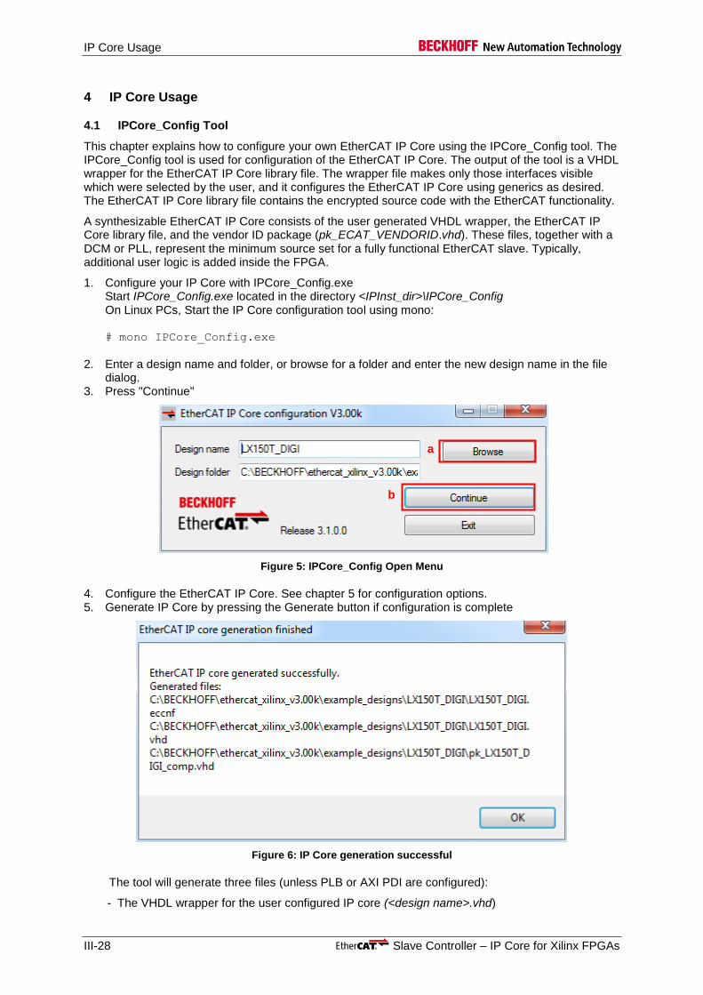
IP Core Usage
III-28 Slave Controller – IP Core for Xilinx FPGAs
4 IP Core Usage
4.1 IPCore_Config Tool
This chapter explains how to configure your own EtherCAT IP Core using the IPCore_Config tool. The IPCore_Config tool is used for configuration of the EtherCAT IP Core. The output of the tool is a VHDL wrapper for the EtherCAT IP Core library file. The wrapper file makes only those interfaces visible which were selected by the user, and it configures the EtherCAT IP Core using generics as desired. The EtherCAT IP Core library file contains the encrypted source code with the EtherCAT functionality.
A synthesizable EtherCAT IP Core consists of the user generated VHDL wrapper, the EtherCAT IP Core library file, and the vendor ID package (pk_ECAT_VENDORID.vhd). These files, together with a DCM or PLL, represent the minimum source set for a fully functional EtherCAT slave. Typically, additional user logic is added inside the FPGA.
1. Configure your IP Core with IPCore_Config.exe Start IPCore_Config.exe located in the directory <IPInst_dir>\IPCore_Config On Linux PCs, Start the IP Core configuration tool using mono: # mono IPCore_Config.exe
2. Enter a design name and folder, or browse for a folder and enter the new design name in the file dialog.
3. Press "Continue"
Figure 5: IPCore_Config Open Menu
4. Configure the EtherCAT IP Core. See chapter 5 for configuration options. 5. Generate IP Core by pressing the Generate button if configuration is complete
Figure 6: IP Core generation successful
The tool will generate three files (unless PLB or AXI PDI are configured):
- The VHDL wrapper for the user configured IP core (<design name>.vhd)
a
b
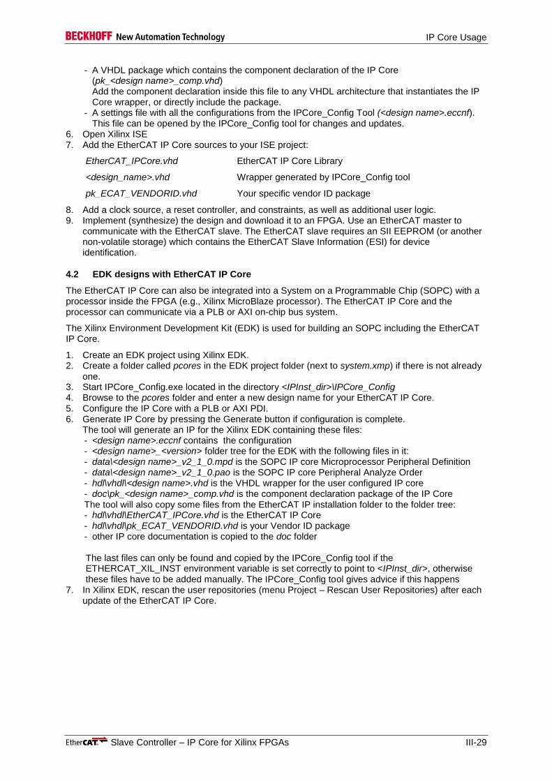
IP Core Usage
Slave Controller – IP Core for Xilinx FPGAs III-29
- A VHDL package which contains the component declaration of the IP Core (pk_<design name>_comp.vhd) Add the component declaration inside this file to any VHDL architecture that instantiates the IP Core wrapper, or directly include the package.
- A settings file with all the configurations from the IPCore_Config Tool (<design name>.eccnf). This file can be opened by the IPCore_Config tool for changes and updates.
6. Open Xilinx ISE 7. Add the EtherCAT IP Core sources to your ISE project:
EtherCAT_IPCore.vhd EtherCAT IP Core Library
<design_name>.vhd Wrapper generated by IPCore_Config tool
pk_ECAT_VENDORID.vhd Your specific vendor ID package
8. Add a clock source, a reset controller, and constraints, as well as additional user logic. 9. Implement (synthesize) the design and download it to an FPGA. Use an EtherCAT master to
communicate with the EtherCAT slave. The EtherCAT slave requires an SII EEPROM (or another non-volatile storage) which contains the EtherCAT Slave Information (ESI) for device identification.
4.2 EDK designs with EtherCAT IP Core
The EtherCAT IP Core can also be integrated into a System on a Programmable Chip (SOPC) with a processor inside the FPGA (e.g., Xilinx MicroBlaze processor). The EtherCAT IP Core and the processor can communicate via a PLB or AXI on-chip bus system.
The Xilinx Environment Development Kit (EDK) is used for building an SOPC including the EtherCAT IP Core.
1. Create an EDK project using Xilinx EDK. 2. Create a folder called pcores in the EDK project folder (next to system.xmp) if there is not already
one. 3. Start IPCore_Config.exe located in the directory <IPInst_dir>\IPCore_Config 4. Browse to the pcores folder and enter a new design name for your EtherCAT IP Core. 5. Configure the IP Core with a PLB or AXI PDI. 6. Generate IP Core by pressing the Generate button if configuration is complete.
The tool will generate an IP for the Xilinx EDK containing these files: - <design name>.eccnf contains the configuration - <design name>_<version> folder tree for the EDK with the following files in it: - data\<design name>_v2_1_0.mpd is the SOPC IP core Microprocessor Peripheral Definition - data\<design name>_v2_1_0.pao is the SOPC IP core Peripheral Analyze Order - hdl\vhdl\<design name>.vhd is the VHDL wrapper for the user configured IP core - doc\pk_<design name>_comp.vhd is the component declaration package of the IP Core The tool will also copy some files from the EtherCAT IP installation folder to the folder tree: - hdl\vhdl\EtherCAT_IPCore.vhd is the EtherCAT IP Core - hdl\vhdl\pk_ECAT_VENDORID.vhd is your Vendor ID package - other IP core documentation is copied to the doc folder The last files can only be found and copied by the IPCore_Config tool if the ETHERCAT_XIL_INST environment variable is set correctly to point to <IPInst_dir>, otherwise these files have to be added manually. The IPCore_Config tool gives advice if this happens
7. In Xilinx EDK, rescan the user repositories (menu Project – Rescan User Repositories) after each update of the EtherCAT IP Core.
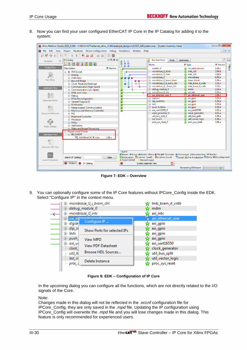
IP Core Usage
III-30 Slave Controller – IP Core for Xilinx FPGAs
8. Now you can find your user configured EtherCAT IP Core in the IP Catalog for adding it to the system:
Figure 7: EDK – Overview
9. You can optionally configure some of the IP Core features without IPCore_Config inside the EDK. Select "Configure IP" in the context menu.
Figure 8: EDK – Configuration of IP Core
In the upcoming dialog you can configure all the functions, which are not directly related to the I/O signals of the Core.
Note: Changes made in this dialog will not be reflected in the .eccnf configuration file for IPCore_Config, they are only saved in the .mpd file. Updating the IP configuration using IPCore_Config will overwrite the .mpd file and you will lose changes made in this dialog. This feature is only recommended for experienced users.

IP Core Usage
Slave Controller – IP Core for Xilinx FPGAs III-31
Figure 9: EDK – Configuration Dialog
10. Assign addresses to the EtherCAT IP Core. The tab "Addresses" in the "System Assembly View" shows the internal addresses of the IP Cores. Press the Generate Addresses button to automatically assign addresses.
Figure 10: EDK – System Assembly View, Addresses tab
Note: If you have added a new IP Core, you can generate or set the internal addresses. The EtherCAT IP core needs at least 64 Kbyte address space. Larger sizes will result in less address decoding logic.
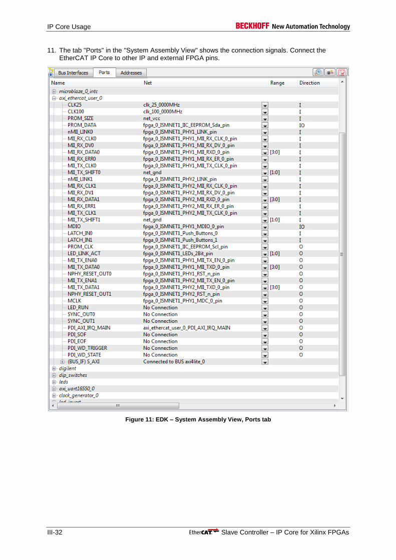
IP Core Usage
III-32 Slave Controller – IP Core for Xilinx FPGAs
11. The tab "Ports" in the "System Assembly View" shows the connection signals. Connect the EtherCAT IP Core to other IP and external FPGA pins.
Figure 11: EDK – System Assembly View, Ports tab
IP Core Usage
Slave Controller – IP Core for Xilinx FPGAs III-33
12. Generate Bitstream Result is the file "system.bit" in the implementation folder of the EDK project. This configuration file only includes the hardware parts of the design, without software for the processor.
13. Create and build a software application (Export Design – Export & Launch SDK 14. Update Bitstream with software program information
(EDK – Device Configuration – Update Bitstream) Result is the file “download.bit” (= “system.bit” + “<software application>.elf”) in the implementation folder of the EDK project.
15. Download the design into your FPGA:
a) Download temporarily into the volatile configuration memory of the FPGA via JTAG-Interface: EDK – Device Configuration – Download Bitstream
b) Download permanently into the non-volatile configuration SPI flash via JTAG-Interface and indirect SPI flash configuration using Xilinx IMPACT.
4.3 Vivado designs with EtherCAT IP Core
There are two basic kinds of implementing the EtherCAT IP core using Vivado:
The first option is characterized by placing the EtherCAT IP core outside of a block design. All IPs are connected inside the block design except for the EtherCAT IP. The AXI connection for the EtherCAT IP is an external connection of the block design. The block design is instantiated on a top-level HDL file, which also instantiates the EtherCAT IP Core.
NOTE: This kind of implementation is shown in the example designs.
The second option is to use the output files of the IPCore_Config tool as input sources for an individual IP packed with the Xilinx IP Packager. In this case, the EtherCAT IP gets another wrapper generated by the IP Packager. The packed IP is added to the block design and connected to other IP.
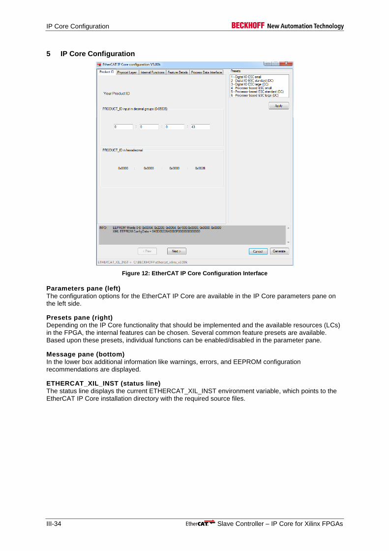
IP Core Configuration
III-34 Slave Controller – IP Core for Xilinx FPGAs
5 IP Core Configuration
Figure 12: EtherCAT IP Core Configuration Interface
Parameters pane (left) The configuration options for the EtherCAT IP Core are available in the IP Core parameters pane on the left side.
Presets pane (right) Depending on the IP Core functionality that should be implemented and the available resources (LCs) in the FPGA, the internal features can be chosen. Several common feature presets are available. Based upon these presets, individual functions can be enabled/disabled in the parameter pane.
Message pane (bottom) In the lower box additional information like warnings, errors, and EEPROM configuration recommendations are displayed.
ETHERCAT_XIL_INST (status line) The status line displays the current ETHERCAT_XIL_INST environment variable, which points to the EtherCAT IP Core installation directory with the required source files.
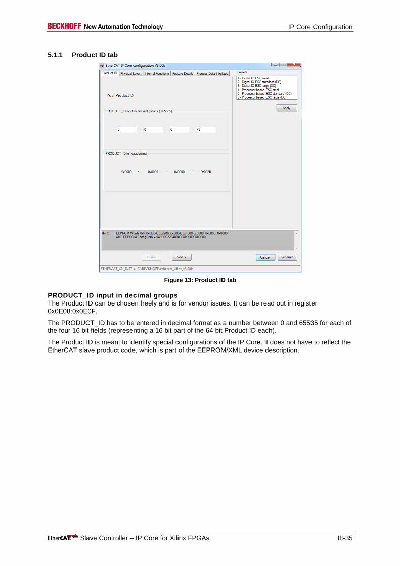
IP Core Configuration
Slave Controller – IP Core for Xilinx FPGAs III-35
5.1.1 Product ID tab
Figure 13: Product ID tab
PRODUCT_ID input in decimal groups The Product ID can be chosen freely and is for vendor issues. It can be read out in register 0x0E08:0x0E0F.
The PRODUCT_ID has to be entered in decimal format as a number between 0 and 65535 for each of the four 16 bit fields (representing a 16 bit part of the 64 bit Product ID each).
The Product ID is meant to identify special configurations of the IP Core. It does not have to reflect the EtherCAT slave product code, which is part of the EEPROM/XML device description.
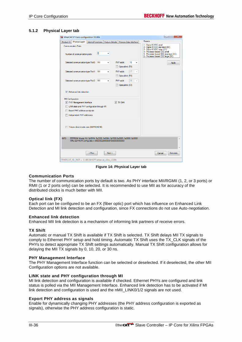
IP Core Configuration
III-36 Slave Controller – IP Core for Xilinx FPGAs
5.1.2 Physical Layer tab
Figure 14: Physical Layer tab
Communication Ports The number of communication ports by default is two. As PHY interface MII/RGMII (1, 2, or 3 ports) or RMII (1 or 2 ports only) can be selected. It is recommended to use MII as for accuracy of the distributed clocks is much better with MII.
Optical link (FX) Each port can be configured to be an FX (fiber optic) port which has influence on Enhanced Link Detection and MI link detection and configuration, since FX connections do not use Auto-negotiation.
Enhanced link detection Enhanced MII link detection is a mechanism of informing link partners of receive errors.
TX Shift Automatic or manual TX Shift is available if TX Shift is selected. TX Shift delays MII TX signals to comply to Ethernet PHY setup and hold timing. Automatic TX Shift uses the TX_CLK signals of the PHYs to detect appropriate TX Shift settings automatically. Manual TX Shift configuration allows for delaying the MII TX signals by 0, 10, 20, or 30 ns.
PHY Management Interface The PHY Management Interface function can be selected or deselected. If it deselected, the other MII Configuration options are not available.
LINK state and PHY configuration through MI MI link detection and configuration is available if checked. Ethernet PHYs are configured and link status is polled via the MII Management Interface. Enhanced link detection has to be activated if MI link detection and configuration is used and the nMII_LINK0/1/2 signals are not used.
Export PHY address as signals Enable for dynamically changing PHY addresses (the PHY address configuration is exported as signals), otherwise the PHY address configuration is static.
IP Core Configuration
Slave Controller – IP Core for Xilinx FPGAs III-37
Independent PHY addresses Enable if the PHY addresses are not consecutive. If enabled, the PHY addresses of each port can be configured individually.
PHY address offset Configure the base PHY address (belonging to port 0) if the PHY addresses are consecutive.
PHY address Configure the individual PHY address of each port
Tristate Driver inside core (EEPROM/MI) If selected tri-state drivers of the core are used for access to EEPROM and PHY Management signals.
This function should not be enabled when the PLB/AXI Process Data Interface is used. This is also marked in the output window at the bottom.
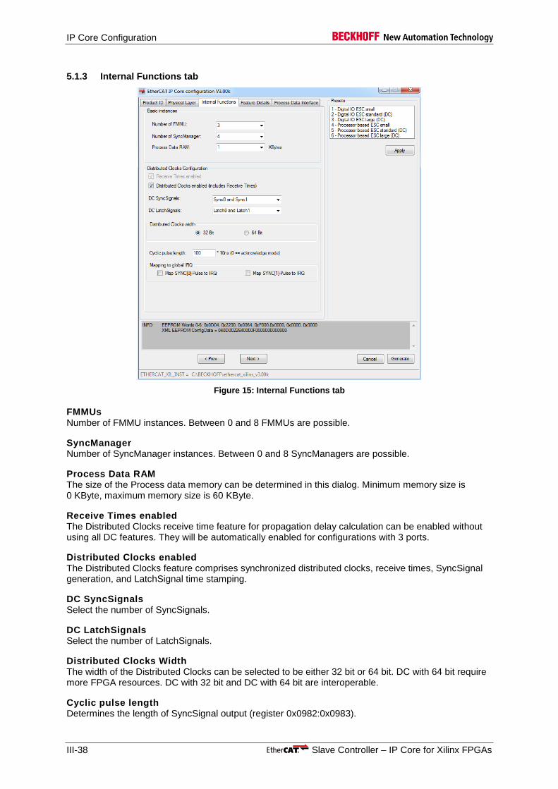
IP Core Configuration
III-38 Slave Controller – IP Core for Xilinx FPGAs
5.1.3 Internal Functions tab
Figure 15: Internal Functions tab
FMMUs Number of FMMU instances. Between 0 and 8 FMMUs are possible.
SyncManager Number of SyncManager instances. Between 0 and 8 SyncManagers are possible.
Process Data RAM The size of the Process data memory can be determined in this dialog. Minimum memory size is 0 KByte, maximum memory size is 60 KByte.
Receive Times enabled The Distributed Clocks receive time feature for propagation delay calculation can be enabled without using all DC features. They will be automatically enabled for configurations with 3 ports.
Distributed Clocks enabled The Distributed Clocks feature comprises synchronized distributed clocks, receive times, SyncSignal generation, and LatchSignal time stamping.
DC SyncSignals Select the number of SyncSignals.
DC LatchSignals Select the number of LatchSignals.
Distributed Clocks Width The width of the Distributed Clocks can be selected to be either 32 bit or 64 bit. DC with 64 bit require more FPGA resources. DC with 32 bit and DC with 64 bit are interoperable.
Cyclic pulse length Determines the length of SyncSignal output (register 0x0982:0x0983).

IP Core Configuration
Slave Controller – IP Core for Xilinx FPGAs III-39
Mapping to global IRQ Sync0 and Sync1 can additionally be mapped internally to the global IRQ. This might be a good solution if a microcontroller interface is short on IRQs. However, the sync signals will remain available on Sync0 and Sync1 outputs.
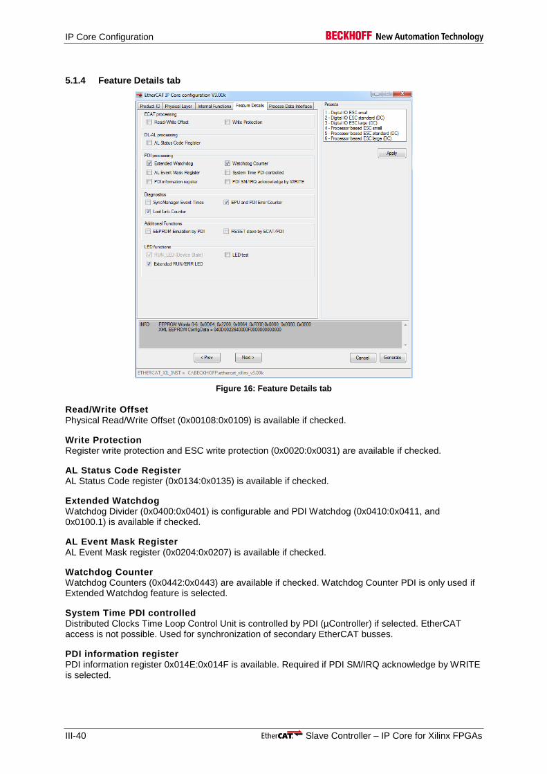
IP Core Configuration
III-40 Slave Controller – IP Core for Xilinx FPGAs
5.1.4 Feature Details tab
Figure 16: Feature Details tab
Read/Write Offset Physical Read/Write Offset (0x00108:0x0109) is available if checked.
Write Protection Register write protection and ESC write protection (0x0020:0x0031) are available if checked.
AL Status Code Register AL Status Code register (0x0134:0x0135) is available if checked.
Extended Watchdog Watchdog Divider (0x0400:0x0401) is configurable and PDI Watchdog (0x0410:0x0411, and 0x0100.1) is available if checked.
AL Event Mask Register AL Event Mask register (0x0204:0x0207) is available if checked.
Watchdog Counter Watchdog Counters (0x0442:0x0443) are available if checked. Watchdog Counter PDI is only used if Extended Watchdog feature is selected.
System Time PDI controlled Distributed Clocks Time Loop Control Unit is controlled by PDI (µController) if selected. EtherCAT access is not possible. Used for synchronization of secondary EtherCAT busses.
PDI information register PDI information register 0x014E:0x014F is available. Required if PDI SM/IRQ acknowledge by WRITE is selected.

IP Core Configuration
Slave Controller – IP Core for Xilinx FPGAs III-41
PDI SM/IRQ acknowledge by WRITE Some ESC functions are triggered by reading from the PDI. Since PDI data bus widths are increasing up to 64 bit and beyond, it is not possible to read individual bytes anymore because most µControllers do not support byte enable signals for read commands. In order to prevent accidentally reading of trigger addresses (like SyncManager buffer end or IRQ acknowledge registers), this option allows to use write commands (with byte enables) to trigger the functions.
SyncManager Event Times Distributed Clocks SyncManager Event Times (0x09F0:0x09FF) are available if checked. Used for debugging SyncManager interactions.
EPU and PDI Error Counter EtherCAT Processing Unit (EPU) and PDI Error counters (0x030C:0x030D) are available if checked.
Lost Link Counter Lost Link Counters (0x0310:0x0313) are available if checked.
EEPROM Emulation by PDI EEPROM is and has to be emulated by a µController with access to a NVRAM. I²C EEPROM is not necessary if EEPROM Emulation is activated, I²C interface is deactivated. Only usable with PDIs for µController connection.
RESET slave by ECAT/PDI The reset registers (0x0040:0x0041) and the RESET_OUT signal is available if this feature is checked.
RUN LED (Device State) RUN LED output indicates AL Status (0x0130) if activated. Otherwise RUN LED has to be controlled by a µController. Always activated if no PDI is selected or if Digital I/O PDI is selected.
Extended RUN/ERR LED Support for ERR LED and STATE LED, direct control of RUN/ERR LED via RUN/ERR LED Override register (0x0138:0x0139).
LED Test A short LED flash after reset for all LED signals is enabled if this feature is selected.
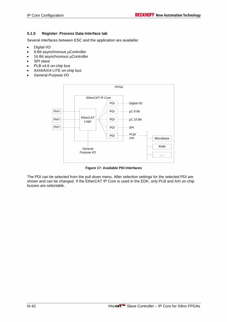
IP Core Configuration
III-42 Slave Controller – IP Core for Xilinx FPGAs
5.1.5 Register: Process Data Interface tab
Several interfaces between ESC and the application are available:
Digital I/O
8 Bit asynchronous µController
16 Bit asynchronous µController
SPI slave
PLB v4.6 on-chip bus
AXI4/AXI4 LITE on-chip bus
General Purpose I/O
EtherCAT
Logic
PDI
PDI
PDI
PDI
SPI
Digital I/O
µC 8 Bit
PLB/
AXI
EtherCAT IP Core
Microblaze
RAM
…..
µC 16 BitPDI
FPGA
PHY
PHY
PHY
General
Purpose I/O
Figure 17: Available PDI Interfaces
The PDI can be selected from the pull down menu. After selection settings for the selected PDI are shown and can be changed. If the EtherCAT IP Core is used in the EDK, only PLB and AXI on-chip busses are selectable.
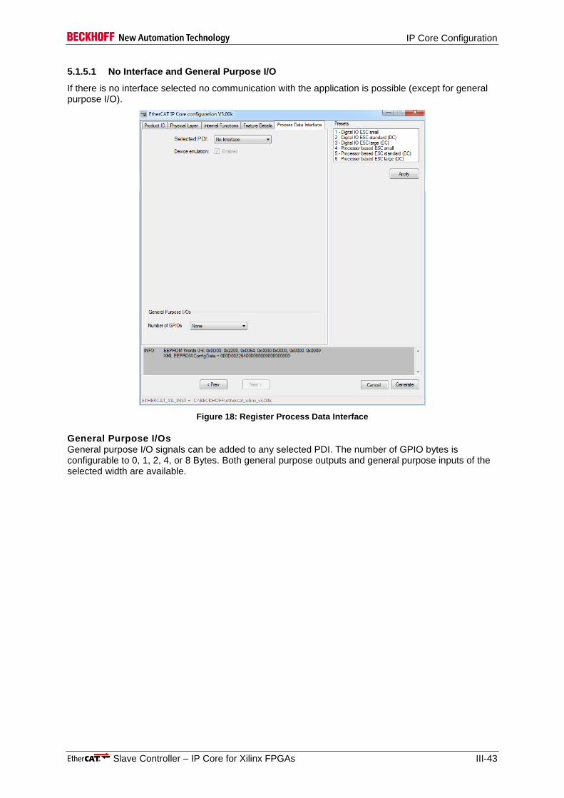
IP Core Configuration
Slave Controller – IP Core for Xilinx FPGAs III-43
5.1.5.1 No Interface and General Purpose I/O
If there is no interface selected no communication with the application is possible (except for general purpose I/O).
Figure 18: Register Process Data Interface
General Purpose I/Os General purpose I/O signals can be added to any selected PDI. The number of GPIO bytes is configurable to 0, 1, 2, 4, or 8 Bytes. Both general purpose outputs and general purpose inputs of the selected width are available.
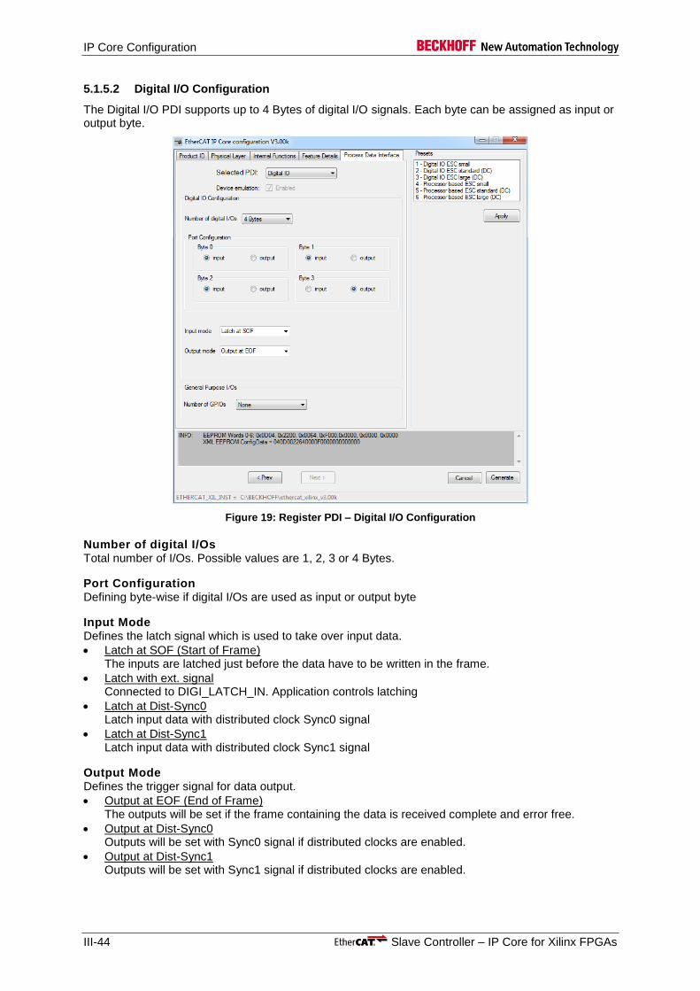
IP Core Configuration
III-44 Slave Controller – IP Core for Xilinx FPGAs
5.1.5.2 Digital I/O Configuration
The Digital I/O PDI supports up to 4 Bytes of digital I/O signals. Each byte can be assigned as input or output byte.
Figure 19: Register PDI – Digital I/O Configuration
Number of digital I/Os Total number of I/Os. Possible values are 1, 2, 3 or 4 Bytes.
Port Configuration Defining byte-wise if digital I/Os are used as input or output byte
Input Mode Defines the latch signal which is used to take over input data.
Latch at SOF (Start of Frame) The inputs are latched just before the data have to be written in the frame.
Latch with ext. signal Connected to DIGI_LATCH_IN. Application controls latching
Latch at Dist-Sync0 Latch input data with distributed clock Sync0 signal
Latch at Dist-Sync1 Latch input data with distributed clock Sync1 signal
Output Mode Defines the trigger signal for data output.
Output at EOF (End of Frame) The outputs will be set if the frame containing the data is received complete and error free.
Output at Dist-Sync0 Outputs will be set with Sync0 signal if distributed clocks are enabled.
Output at Dist-Sync1 Outputs will be set with Sync1 signal if distributed clocks are enabled.
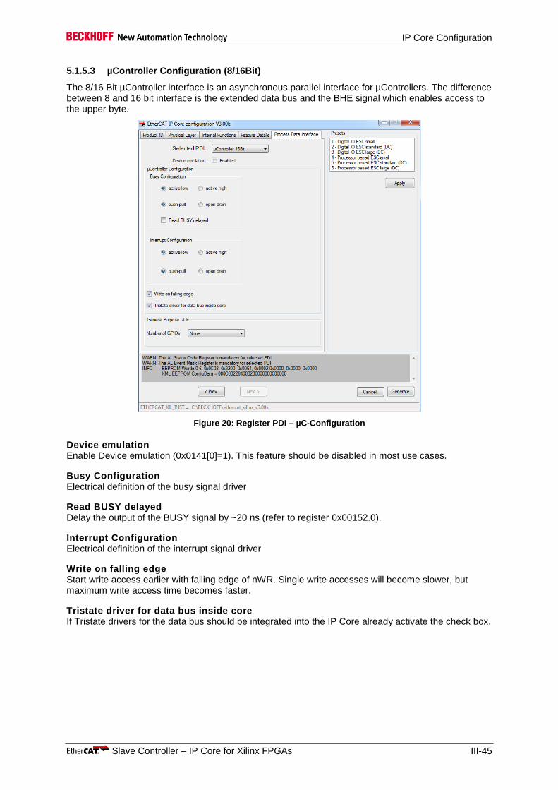
IP Core Configuration
Slave Controller – IP Core for Xilinx FPGAs III-45
5.1.5.3 µController Configuration (8/16Bit)
The 8/16 Bit µController interface is an asynchronous parallel interface for µControllers. The difference between 8 and 16 bit interface is the extended data bus and the BHE signal which enables access to the upper byte.
Figure 20: Register PDI – µC-Configuration
Device emulation Enable Device emulation (0x0141[0]=1). This feature should be disabled in most use cases.
Busy Configuration Electrical definition of the busy signal driver
Read BUSY delayed Delay the output of the BUSY signal by ~20 ns (refer to register 0x00152.0).
Interrupt Configuration Electrical definition of the interrupt signal driver
Write on falling edge Start write access earlier with falling edge of nWR. Single write accesses will become slower, but maximum write access time becomes faster.
Tristate driver for data bus inside core If Tristate drivers for the data bus should be integrated into the IP Core already activate the check box.
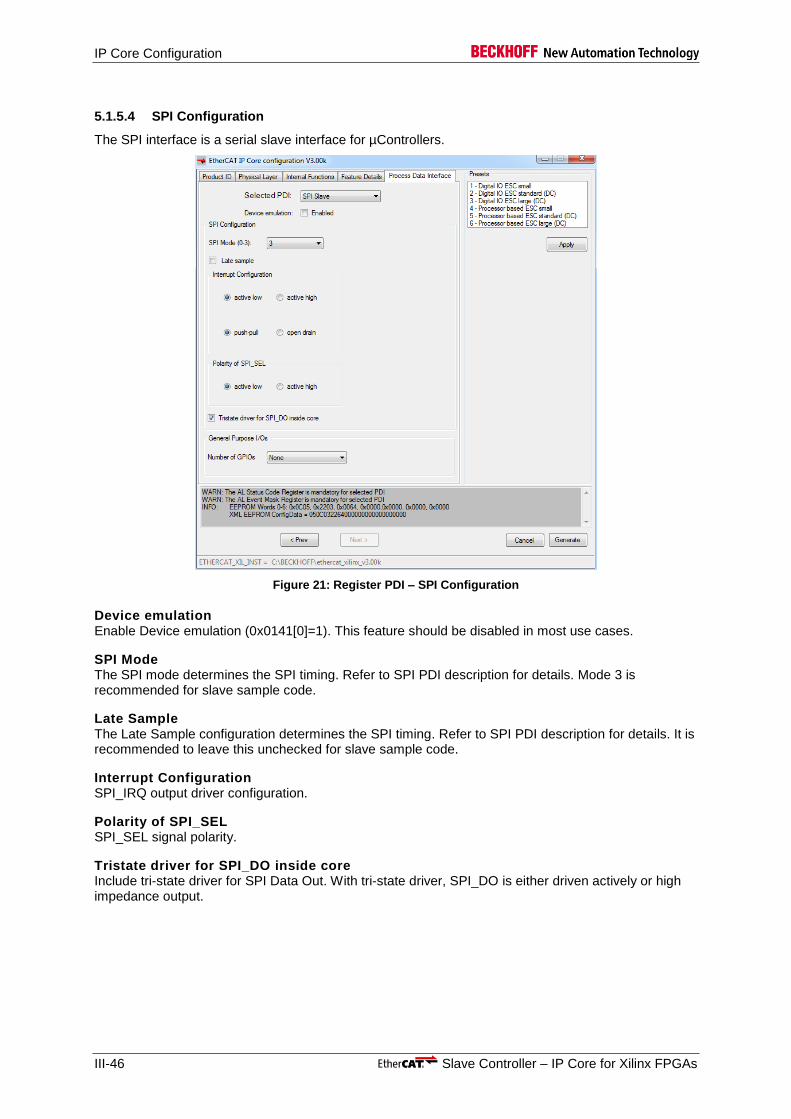
IP Core Configuration
III-46 Slave Controller – IP Core for Xilinx FPGAs
5.1.5.4 SPI Configuration
The SPI interface is a serial slave interface for µControllers.
Figure 21: Register PDI – SPI Configuration
Device emulation Enable Device emulation (0x0141[0]=1). This feature should be disabled in most use cases.
SPI Mode The SPI mode determines the SPI timing. Refer to SPI PDI description for details. Mode 3 is recommended for slave sample code.
Late Sample The Late Sample configuration determines the SPI timing. Refer to SPI PDI description for details. It is recommended to leave this unchecked for slave sample code.
Interrupt Configuration SPI_IRQ output driver configuration.
Polarity of SPI_SEL SPI_SEL signal polarity.
Tristate driver for SPI_DO inside core Include tri-state driver for SPI Data Out. With tri-state driver, SPI_DO is either driven actively or high impedance output.

IP Core Configuration
Slave Controller – IP Core for Xilinx FPGAs III-47
5.1.5.5 Processor Local Bus (PLB) Configuration
The PLB v4.6 PDI connects the IP Core with a PLB Master (e.g. Xilinx MicroBlazeTM). The data bus with is 32 bit, and the address bus is also 32 bit wide.
Figure 22: Register PDI – PLB Interface Configuration
Device emulation Enable Device emulation (0x0141[0]=1). This feature should be disabled in most use cases.
On-Chip Bus CLK is asynchronous to CLK25 core clock Enable if the On-chip BUS CLK is asynchronous to CLK25. Additional synchronization stages are added in this case.
Interrupt type Select the usage type of the interrupt signal (level or edge). Since the main interrupt can have different sources, a level based interrupt is typically required.
Generate pcore for XPS Enable generation of an EtherCAT IP Core package for Xilinx XPS/EDK, i.e., a pcores folder structure with source files and module definitions.
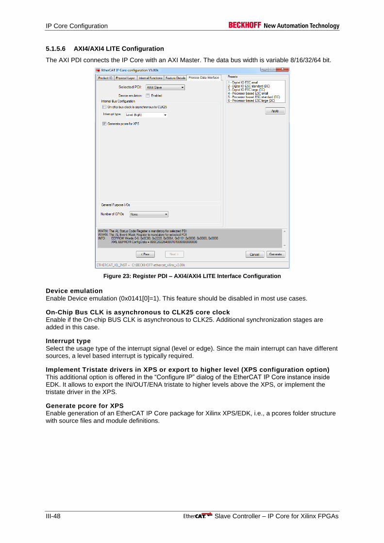
IP Core Configuration
III-48 Slave Controller – IP Core for Xilinx FPGAs
5.1.5.6 AXI4/AXI4 LITE Configuration
The AXI PDI connects the IP Core with an AXI Master. The data bus width is variable 8/16/32/64 bit.
Figure 23: Register PDI – AXI4/AXI4 LITE Interface Configuration
Device emulation Enable Device emulation (0x0141[0]=1). This feature should be disabled in most use cases.
On-Chip Bus CLK is asynchronous to CLK25 core clock Enable if the On-chip BUS CLK is asynchronous to CLK25. Additional synchronization stages are added in this case.
Interrupt type Select the usage type of the interrupt signal (level or edge). Since the main interrupt can have different sources, a level based interrupt is typically required.
Implement Tristate drivers in XPS or export to higher level (XPS configuration option) This additional option is offered in the “Configure IP” dialog of the EtherCAT IP Core instance inside EDK. It allows to export the IN/OUT/ENA tristate to higher levels above the XPS, or implement the tristate driver in the XPS.
Generate pcore for XPS Enable generation of an EtherCAT IP Core package for Xilinx XPS/EDK, i.e., a pcores folder structure with source files and module definitions.

Example Designs
Slave Controller – IP Core for Xilinx FPGAs III-49
6 Example Designs
Example designs are available for:
Avnet Xilinx Spartan-6 LX150T Development Kit with MII and Digital I/O PDI
Avnet Xilinx Spartan-6 LX150T Development Kit with MII, AXI PDI, and Microblaze processor
Xilinx Zynq ZC702 Development Kit with MII, AXI PDI, and ARM processor (Vivado based)
The EtherCAT master uses an XML file which describes the device and its features. The XML device description file for all example designs and its schema can be found in the installation directory.
<IPInst_dir>\example_designs\EtherCAT_Device_Description\
Projects have to be compiled and then can be loaded to the SPI configuration EEPROM of the evaluation board.
The EtherCAT IP core resource consumption figures are based on EtherCAT IP Core for Xilinx FPGAs Version 3.00c and Xilinx ISE 14.5.
PHY strapping options on Xilinx ISMNET PHY board Some Ethernet PHYs, and especially the PHYs on the Xilinx ISMNET PHY board use the communication signals for strapping configuration signals. If these signals are not used by the FPGA design, take care that the strapping values are not changed by default IO behaviour. Due to this fact, the COL and CRS signals of the PHYs are declared as inputs in the example designs. In this way, these two signals are not driven or pulled up/down by the FPGA, so the configuration resistors on the ISMNET define the configuration.

Example Designs
III-50 Slave Controller – IP Core for Xilinx FPGAs
6.1 Avnet Xilinx Spartan-6 LX150T Development Kit with Digital I/O
6.1.1 Configuration and resource consumption
Table 13: Resource consumption Avnet LX150T example design
Configuration Resources XC6SLX150T
Physical layer 2x MII, TX Shift, MIIM, Enhanced Link Detection
Slice Registers 7,552 4 %
Internal Function 3x FMMU 4x SyncManager
1 KB RAM
Slice LUTs 8,969 9 %
Distributed clocks 32 bit, 2x Sync, 2x Latch
Occupied Slices 3,408 14 %
Feature details Extended Watchdog,
Watchdog counter,
EPU and PDI Error Counter,
Lost link counter,
RUN_LED, Extended RUN/ERR LED
Block RAM RAMB8BWER RAMB16BWER
2 0
1 % 0 %
PDI Digital I/O: 3 Byte IN, 1 Byte OUT
DCM 1 8 %
6.1.2 Functionality
Attach the FMC ISMNET module to FMC1 connector of LX150T base board. Populate jumper JP6 pins 1-2 (CARRIER_25MHz to CARRIER_25MHZ_S) on ISMNET, because the 25 MHz clock source for the Ethernet PHYs is also used as the clock source for the whole system including EtherCAT IP core in the Spartan-6 LX150T FPGA. Configure FMC IO voltage to 2.5V. You can optionally connect the UART or the LX150T (JR1) to your PC (9600 baud, 8 bit data, 1 stop bit, no parity, no hardware handshake). The LEDs D3 and D4 on the FMC ISMNET module are used as Link/Activity LEDs for the two Ethernet ports.
Functionality of the Digital I/O example design:
Digital input data from push buttons SW3-SW5 on the LX150T are available in the Process Data RAM 0x1000[2:0]
Digital input data from DIP switches SW6 on the LX150T are available in the Process Data RAM 0x1001
Digital input data from push buttons SW1-SW2 on the ISMNET module are available in the Process Data RAM 0x1002[1:0]
Digital input data from DIP switches SW3 on the ISMNET module are available in the Process Data RAM 0x1002[7:4]
Digital output data from Digital Output register (0x0F03) is visualized with LEDs D7-D14 on the LX150T
DC LatchSignals are connected to push buttons SW1-SW2 on the ISMNET module
6.1.3 Implementation
1. Open Xilinx ISE 2. Open example design
<IPInst_dir>\example_designs\LX150T_DIGI.xise 3. Generate Programming File 4. Download bitstream to FPGA

Example Designs
Slave Controller – IP Core for Xilinx FPGAs III-51
6.1.4 SII EEPROM
Use this ESI for the SII EEPROM:
Beckhoff Automation GmbH (Evaluation)/ IP Core example designs ET1815 (Xilinx)/ ET1815 IP Core Avnet LX150T DIGI
6.1.5 Downloadable configuration file
An already synthesized time limited configuration file
LX150T_DIGI_Demo_V3_00c_time_limited.bit
based on this example design can be found in the
<IPInst_dir>\example_designs\LX150T_DIGI\
folder. After expiration of about 1 hour the design quits its operation. These files must only be used for evaluation purposes, any distribution is not allowed.

Example Designs
III-52 Slave Controller – IP Core for Xilinx FPGAs
6.2 Avnet Xilinx Spartan-6 LX150T Development Kit with AXI
6.2.1 Configuration and resource consumption
Table 14: Resource consumption Avnet LX150T example design
Configuration Resources XC6SLX150T
Physical layer 2x MII, TX Shift, MIIM
Slice Registers 10,354 5 %
Internal Function 4x FMMU 4x SyncManager
1 KB RAM
Slice LUTs 13,935 16 %
Distributed clocks 32 bit, 2x Sync, 2x Latch
Occupied Slices 5,443 23 %
Feature details AL Status Code register,
Extended Watchdog,
Watchdog counter,
AL Event Mask reg.
EPU and PDI Error Counter,
Lost link counter,
RUN_LED, LED Test
Block RAM RAMB8BWER RAMB16BWER
2 16
1 % 5 %
PDI AXI4 LITE slave, 32 bit PLL 1 16 %
6.2.2 Functionality
Attach the FMC ISMNET module to FMC1 connector of LX150T base board. Populate jumper JP6 pins 1-2 (CARRIER_25MHz to CARRIER_25MHZ_S) on ISMNET, because the 25 MHz clock source for the Ethernet PHYs is also used as the clock source for the whole system including EtherCAT IP core in the Spartan-6 LX150T FPGA. Configure FMC IO voltage to 2.5V. You can optionally connect the UART or the LX150T (JR1) to your PC (9600 baud, 8 bit data, 1 stop bit, no parity, no hardware handshake). The LEDs D3 and D4 on the FMC ISMNET module are used as Link/Activity LEDs for the two Ethernet ports. Push button SW2 on the LX150T is used as system reset input.
The Microblaze demo application performs the following tasks:
Accept any EtherCAT Slave State request (copying AL Control to AL Status register). Print state changes via UART.
Copy output data from EtherCAT IP Core (0x1024) to GPIO for LEDs D7-D14 on the LX150T.
Copy output data from EtherCAT IP Core (0x1004) to GPIO for DIGILENT U15 on the ISMNET.
Print output data from the EtherCAT IP Core (0x1020-0x1023) via UART.
Copy input data from GPIO for push buttons SW3-SW5 on the LX150T to the EtherCAT IP Core (0x1000).
Copy input data from GPIO for push buttons SW1-SW2 on the ISMNET module to the EtherCAT IP Core (0x1002).
Copy input data from GPIO for DIP switches SW6 on the LX150T to the EtherCAT IP Core (0x1001).
Copy input data from GPIO for DIP switches SW3 on the ISMNET module to the EtherCAT IP Core (0x1003).

Example Designs
Slave Controller – IP Core for Xilinx FPGAs III-53
6.2.3 Implementation
1. Open Xilinx EDK 2. Open project:
<IPInst_dir>\ example_designs\LX150T_AXI\system.xmp 3. Generate Bitstream 4. Export Design 5. Launch SDK 6. In SDK, select menu File – New – Application Project 7. Enter a project name, and select project template “BECKHOFF EtherCAT LX150T AXI” 8. Select Next, then Finish. 9. Wait until the projects are built automatically, or select menu Project – Build All 10. Update Bitstream with application image and download to FPGA by selecting menu Xilinx Tools –
Program FPGA Result is the file “download.bit” (= “system.bit” + “<application>.elf”) in the implementation folder of the EDK project.
6.2.4 SII EEPROM
Use this ESI for the SII EEPROM:
Beckhoff Automation GmbH (Evaluation)/ IP Core example designs ET1815 (Xilinx)/ ET1815 IP Core Avnet LX150T
6.2.5 Downloadable configuration file
An already synthesized time limited configuration file
LX150T_AXI_Demo_V3_00c_time_limited.bit
based on this example design can be found in the
<IPInst_dir>\example_designs\LX150T_AXI\
folder. After expiration of about 1 hour the design quits its operation. These files must only be used for evaluation purposes, any distribution is not allowed.

Example Designs
III-54 Slave Controller – IP Core for Xilinx FPGAs
6.3 Xilinx Zynq ZC702 Development Kit with AXI (Vivado based)
6.3.1 Configuration and resource consumption
Table 15: Resource consumption Xilinx Zynq ZC702 example design
Configuration Resources XZ7Z020
Physical layer 2x MII, TX Shift, MIIM
Slice Registers 13,467 13 %
Internal Function 4x FMMU 4x SyncManager
1 KB RAM
Slice LUTs 16,360 31 %
Distributed clocks 32 bit, 2x Sync, 2x Latch
Occupied Slices 5,651 42 %
Feature details AL Status Code register,
Extended Watchdog,
Watchdog counter,
AL Event Mask reg.
EPU and PDI Error Counter,
Lost link counter,
RUN_LED, LED Test
Block RAM RAMB18E1 RAMB36E1
2 1
1 % 1 %
PDI AXI4 LITE slave, 32 bit, asynchronous
MMCME2_ADV 1 25 %
NOTE: These resource consumption figures are based on EtherCAT IP Core for Xilinx FPGAs Version 3.00j and Vivado 2014.2 with AR61518 and the appropriate settings for this answer record.
6.3.2 Functionality
Attach the FMC ISMNET module to FMC1 connector of ZC702 base board. Populate jumper JP6 pins 1-2 (CARRIER_25MHz to CARRIER_25MHZ_S) on ISMNET, because the 25 MHz clock source for the Ethernet PHYs is also used as the clock source for the EtherCAT IP core in the Zynq FPGA. You can optionally connect the UART of the ZC702 (J17) to your PC (9600 baud, 8 bit data, 1 stop bit, no parity, no hardware handshake). The LEDs D3 and D4 on the FMC ISMNET module are used as Link/Activity LEDs for the two Ethernet ports. Push button SW2 on the ZC702 is used as system reset input.
The EtherCAT IP Core and the ISMNET PHY ports are only powered and running if the processor system is running.
The ARM demo application performs the following tasks:
Accept any EtherCAT Slave State request (copying AL Control to AL Status register). Print state changes via UART.
Copy output data from EtherCAT IP Core (0x1024) to GPIO for LEDs DS15-DS22 on the ZC702.
Print output data from the EtherCAT IP Core (0x1020-0x1023) via UART.
Copy input data from GPIO for push buttons SW5/SW7 on the ZC702 to the EtherCAT IP Core (0x1000).
Copy input data from GPIO for push buttons SW1-SW2 on the ISMNET module to the EtherCAT IP Core (0x1002).
Copy input data from GPIO for DIP switches SW12 on the ZC702 to the EtherCAT IP Core (0x1001).
Copy input data from GPIO for DIP switches SW3 on the ISMNET module to the EtherCAT IP Core (0x1003).
Copy input data from GPIO for DIGILENT U15 on the ISMNET module to the EtherCAT IP Core (0x1004).

Example Designs
Slave Controller – IP Core for Xilinx FPGAs III-55
6.3.3 Implementation
1. Open Xilinx Vivado 2. Open project:
<IPInst_dir>\example_designs\ZC702_AXI_VIVADO\ZC702_AXI_VIOVADO.xpr 3. Generate Bitstream 4. Select menu File – Export – Export hardware, and export the hardware description 5. Launch Vivado SDK 6. In SDK, select menu File – New – Application Project 7. Create a First Stage Boot Loader (FSBL) project for the Zynq 8. In SDK, select menu File – New – Application Project 9. Enter a project name, and select project template “BECKHOFF EtherCAT ZC702 AXI” 10. Select Next, then Finish. 11. Select menu Project – Build All 12. Select Xilinx Tools – Create Zynq Boot Image 13. Add First Stage Boot Loader ELF, FPGA bitstream, and Demo application ELF files 14. Place resulting .bin file in the root folder of the SD card, rename the file to BOOT.bin and configure
the ZC702 to boot from SD card.
6.3.4 SII EEPROM
Use this ESI for the SII EEPROM:
Beckhoff Automation GmbH (Evaluation)/ IP Core example designs ET1815 (Xilinx)/ ET1815 IP Core Xilinx ZC702

FPGA Resource Consumption
III-56 Slave Controller – IP Core for Xilinx FPGAs
7 FPGA Resource Consumption
The resource consumption figures shown in this chapter reflect results of example synthesis runs and can only be used for rough resource estimations. The figures are subject to quite large variations depending on design tools and version, FPGA type, constraints (e.g., area vs. speed), total FPGA utilization (design tools typically stop optimization if the timing goal is reached), etc. No extra effort was undertaken to achieve optimum results, i.e. by sophisticated constraining and design flow setting.
For accurate resource consumption figures, please use the evaluation license of the EtherCAT IP Core and synthesize your individual configuration for the desired FPGA.
The figures of the following table do not imply that the individual features are operational in the selected FPGA (i.e., that the resources are sufficient or that timing closure is achievable). The synthesis runs where performed without timing constraints, without location constraints, and without bitstream generation.
The EtherCAT IP core resource consumption overview figures are based on EtherCAT IP Core for Xilinx FPGAs Version 3.00c, Xilinx ISE 14.5, and Xilinx Spartan-6 devices. One Spartan-6 slice contains 4 lookup-tables (LUT6) and 4 flip-flops. The registers and logic LUT figures are subject to variation as a result of optimization. Slice figures are not given any more since their variation is extremely high.
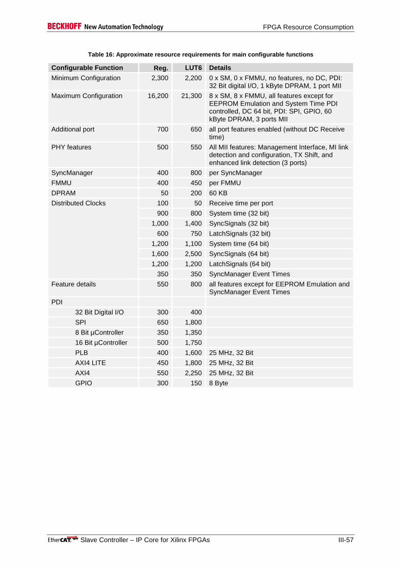
FPGA Resource Consumption
Slave Controller – IP Core for Xilinx FPGAs III-57
Table 16: Approximate resource requirements for main configurable functions
Configurable Function Reg. LUT6 Details
Minimum Configuration 2,300 2,200 0 x SM, 0 x FMMU, no features, no DC, PDI: 32 Bit digital I/O, 1 kByte DPRAM, 1 port MII
Maximum Configuration 16,200 21,300 8 x SM, 8 x FMMU, all features except for EEPROM Emulation and System Time PDI controlled, DC 64 bit, PDI: SPI, GPIO, 60 kByte DPRAM, 3 ports MII
Additional port 700 650 all port features enabled (without DC Receive time)
PHY features 500 550 All MII features: Management Interface, MI link detection and configuration, TX Shift, and enhanced link detection (3 ports)
SyncManager 400 800 per SyncManager
FMMU 400 450 per FMMU
DPRAM 50 200 60 KB
Distributed Clocks 100 50 Receive time per port
900 800 System time (32 bit)
1,000 1,400 SyncSignals (32 bit)
600 750 LatchSignals (32 bit)
1,200 1,100 System time (64 bit)
1,600 2,500 SyncSignals (64 bit)
1,200 1,200 LatchSignals (64 bit)
350 350 SyncManager Event Times
Feature details 550 800 all features except for EEPROM Emulation and SyncManager Event Times
PDI
32 Bit Digital I/O 300 400
SPI 650 1,800
8 Bit µController 350 1,350
16 Bit µController 500 1,750
PLB 400 1,600 25 MHz, 32 Bit
AXI4 LITE 450 1,800 25 MHz, 32 Bit
AXI4 550 2,250 25 MHz, 32 Bit
GPIO 300 150 8 Byte
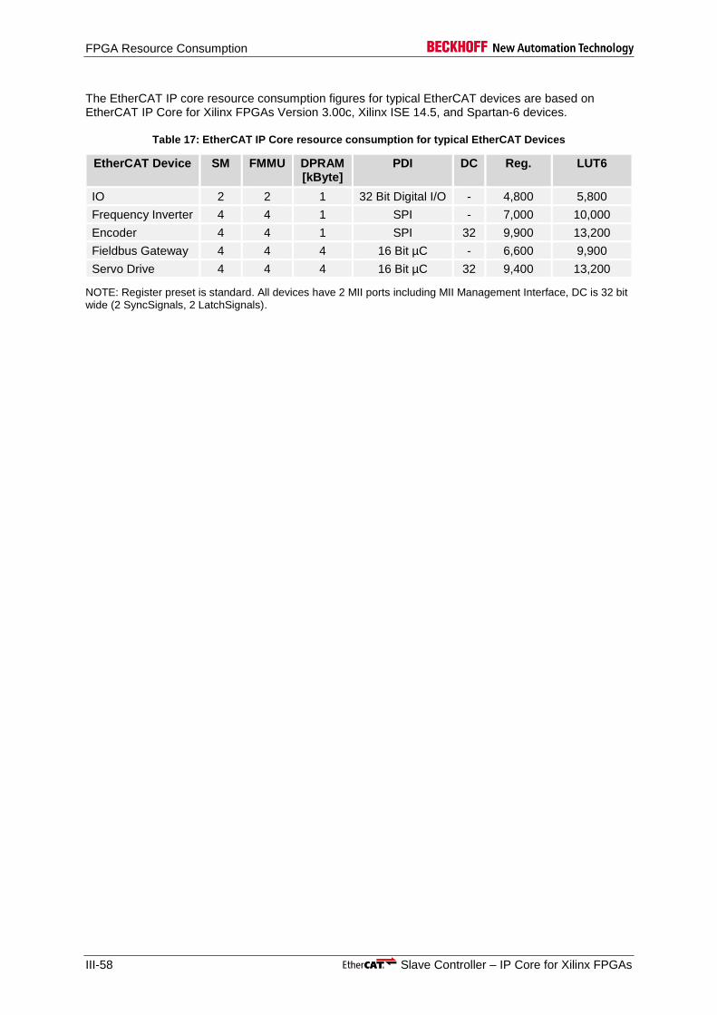
FPGA Resource Consumption
III-58 Slave Controller – IP Core for Xilinx FPGAs
The EtherCAT IP core resource consumption figures for typical EtherCAT devices are based on EtherCAT IP Core for Xilinx FPGAs Version 3.00c, Xilinx ISE 14.5, and Spartan-6 devices.
Table 17: EtherCAT IP Core resource consumption for typical EtherCAT Devices
EtherCAT Device SM FMMU DPRAM [kByte]
PDI DC Reg.
LUT6
IO 2 2 1 32 Bit Digital I/O - 4,800 5,800
Frequency Inverter 4 4 1 SPI - 7,000 10,000
Encoder 4 4 1 SPI 32 9,900 13,200
Fieldbus Gateway 4 4 4 16 Bit µC - 6,600 9,900
Servo Drive 4 4 4 16 Bit µC 32 9,400 13,200
NOTE: Register preset is standard. All devices have 2 MII ports including MII Management Interface, DC is 32 bit wide (2 SyncSignals, 2 LatchSignals).
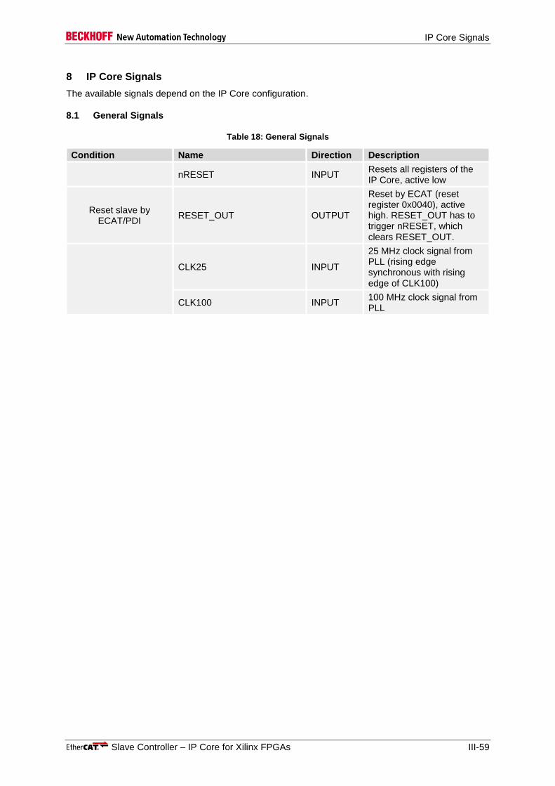
IP Core Signals
Slave Controller – IP Core for Xilinx FPGAs III-59
8 IP Core Signals
The available signals depend on the IP Core configuration.
8.1 General Signals
Table 18: General Signals
Condition Name Direction Description
nRESET INPUT Resets all registers of the IP Core, active low
Reset slave by ECAT/PDI
RESET_OUT OUTPUT
Reset by ECAT (reset register 0x0040), active high. RESET_OUT has to trigger nRESET, which clears RESET_OUT.
CLK25 INPUT
25 MHz clock signal from PLL (rising edge synchronous with rising edge of CLK100)
CLK100 INPUT 100 MHz clock signal from PLL
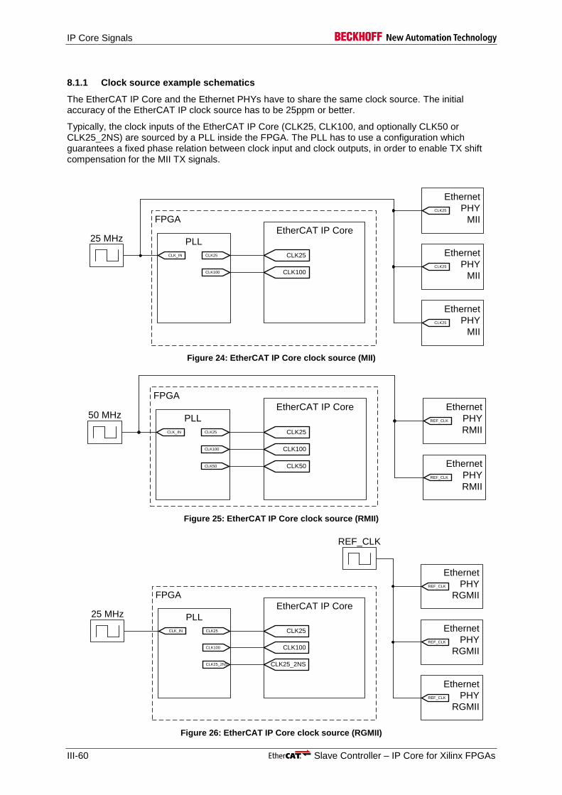
IP Core Signals
III-60 Slave Controller – IP Core for Xilinx FPGAs
8.1.1 Clock source example schematics
The EtherCAT IP Core and the Ethernet PHYs have to share the same clock source. The initial accuracy of the EtherCAT IP clock source has to be 25ppm or better.
Typically, the clock inputs of the EtherCAT IP Core (CLK25, CLK100, and optionally CLK50 or CLK25_2NS) are sourced by a PLL inside the FPGA. The PLL has to use a configuration which guarantees a fixed phase relation between clock input and clock outputs, in order to enable TX shift compensation for the MII TX signals.
CLK25
EtherCAT IP Core
Ethernet
PHY
MIICLK25
PLL
CLK_IN CLK25
CLK100 CLK100
Ethernet
PHY
MIICLK25
25 MHz
Ethernet
PHY
MIICLK25
FPGA
Figure 24: EtherCAT IP Core clock source (MII)
CLK25
EtherCAT IP Core Ethernet
PHY
RMIIREF_CLKPLL
CLK_IN CLK25
CLK100 CLK100
Ethernet
PHY
RMIIREF_CLK
50 MHz
CLK50 CLK50
FPGA
Figure 25: EtherCAT IP Core clock source (RMII)
CLK25
EtherCAT IP Core
Ethernet
PHY
RGMIIREF_CLK
PLL
CLK_IN CLK25
CLK100 CLK100
Ethernet
PHY
RGMIIREF_CLK
25 MHz
Ethernet
PHY
RGMIIREF_CLK
FPGA
REF_CLK
CLK25_2NSCLK25_2NS
Figure 26: EtherCAT IP Core clock source (RGMII)
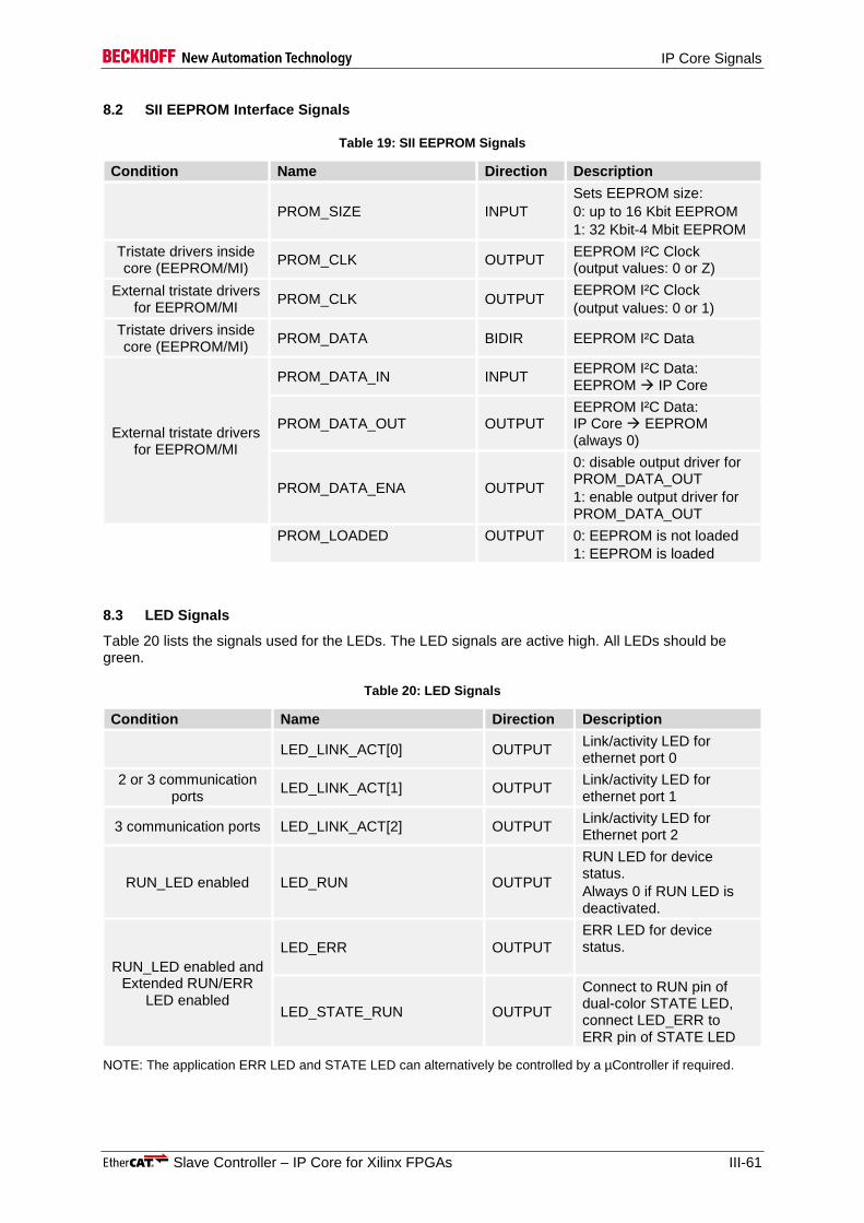
IP Core Signals
Slave Controller – IP Core for Xilinx FPGAs III-61
8.2 SII EEPROM Interface Signals
Table 19: SII EEPROM Signals
Condition Name Direction Description
PROM_SIZE INPUT
Sets EEPROM size:
0: up to 16 Kbit EEPROM
1: 32 Kbit-4 Mbit EEPROM
Tristate drivers inside core (EEPROM/MI)
PROM_CLK OUTPUT EEPROM I²C Clock (output values: 0 or Z)
External tristate drivers for EEPROM/MI
PROM_CLK OUTPUT EEPROM I²C Clock
(output values: 0 or 1)
Tristate drivers inside core (EEPROM/MI)
PROM_DATA BIDIR EEPROM I²C Data
External tristate drivers for EEPROM/MI
PROM_DATA_IN INPUT EEPROM I²C Data: EEPROM IP Core
PROM_DATA_OUT OUTPUT EEPROM I²C Data: IP Core EEPROM (always 0)
PROM_DATA_ENA OUTPUT
0: disable output driver for PROM_DATA_OUT
1: enable output driver for PROM_DATA_OUT
PROM_LOADED OUTPUT 0: EEPROM is not loaded
1: EEPROM is loaded
8.3 LED Signals
Table 20 lists the signals used for the LEDs. The LED signals are active high. All LEDs should be green.
Table 20: LED Signals
Condition Name Direction Description
LED_LINK_ACT[0] OUTPUT Link/activity LED for ethernet port 0
2 or 3 communication ports
LED_LINK_ACT[1] OUTPUT Link/activity LED for ethernet port 1
3 communication ports LED_LINK_ACT[2] OUTPUT Link/activity LED for Ethernet port 2
RUN_LED enabled LED_RUN OUTPUT
RUN LED for device status.
Always 0 if RUN LED is deactivated.
RUN_LED enabled and Extended RUN/ERR
LED enabled
LED_ERR OUTPUT
ERR LED for device status.
LED_STATE_RUN OUTPUT
Connect to RUN pin of dual-color STATE LED, connect LED_ERR to ERR pin of STATE LED
NOTE: The application ERR LED and STATE LED can alternatively be controlled by a µController if required.

IP Core Signals
III-62 Slave Controller – IP Core for Xilinx FPGAs
8.4 Distributed Clocks SYNC/LATCH Signals
Table 21 lists the signals used with Distributed Clocks.
Table 21: DC SYNC/LATCH signals
Condition Name Direction Description
Distributed Clocks and SYNC0 enabled
SYNC_OUT0 OUTPUT DC sync output 0
Distributed Clocks and SYNC0+1 enabled
SYNC_OUT1 OUTPUT DC sync output 1
Distributed Clocks and Latch0 enabled
LATCH_IN0 INPUT DC latch input 0
Distributed Clocks and Latch0+1 enabled
LATCH_IN1 INPUT DC latch input 1
NOTE: SYNC_OUT0/1 are active high/push-pull outputs.

IP Core Signals
Slave Controller – IP Core for Xilinx FPGAs III-63
8.5 Physical Layer Interface
The IP Core is connected with Ethernet PHYs using MII/RMII/RGMII interfaces.
Table 22 lists the general PHY interface signals.
Table 22: Physical Layer General
Condition Name Direction Description
PHY Management Interface enabled and
Export PHY address as signals and
not(Independent PHY addresses)
PHY_OFFSET_VEC[4:0] INPUT PHY address offset
PHY Management Interface enabled and
Export PHY address as signals and
Independent PHY addresses
PHY_ADR_PORT0[4:0] INPUT PHY address port 0
PHY Management Interface enabled and
Export PHY address as signals and
Independent PHY addresses and Port1
PHY_ADR_PORT1[4:0] INPUT PHY address port 1
PHY Management Interface enabled and
Export PHY address as signals and
Independent PHY addresses and Port2
PHY_ADR_PORT2[4:0] INPUT PHY address port 2
Port0 enabled nPHY_RESET_OUT0 OUTPUT PHY reset port 0 (act. low)
Port1 enabled nPHY_RESET_OUT1 OUTPUT PHY reset port 1 (act. low)
Port2 enabled nPHY_RESET_OUT2 OUTPUT PHY reset port 2 (act. low)
PHY Management Interface enabled
MCLK OUTPUT PHY management clock
PHY Management Interface enabled,
Tristate drivers inside core (EEPROM/MII)
MDIO BIDIR PHY management data
PHY Management Interface enabled,
External tristate drivers for EEPROM/MI
MDIO_DATA_IN INPUT PHY management data: PHY IP Core
MDIO_DATA_OUT OUTPUT PHY management data: IP Core PHY
MDIO_DATA_ENA OUTPUT 0: disable output driver for MDIO_DATA_OUT
1: enable output driver for MDIO_DATA_OUT
NOTE: MDIO must have a pull-up resistor (4.7kΩ recommended for ESCs).
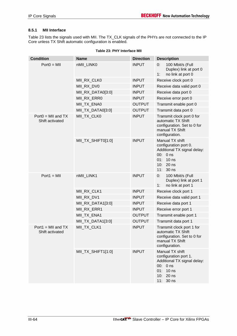
IP Core Signals
III-64 Slave Controller – IP Core for Xilinx FPGAs
8.5.1 MII Interface
Table 23 lists the signals used with MII. The TX_CLK signals of the PHYs are not connected to the IP Core unless TX Shift automatic configuration is enabled.
Table 23: PHY Interface MII
Condition Name Direction Description
Port0 = MII nMII_LINK0 INPUT 0: 100 Mbit/s (Full Duplex) link at port 0
1: no link at port 0
MII_RX_CLK0 INPUT Receive clock port 0
MII_RX_DV0 INPUT Receive data valid port 0
MII_RX_DATA0[3:0] INPUT Receive data port 0
MII_RX_ERR0 INPUT Receive error port 0
MII_TX_ENA0 OUTPUT Transmit enable port 0
MII_TX_DATA0[3:0] OUTPUT Transmit data port 0
Port0 = MII and TX Shift activated
MII_TX_CLK0 INPUT Transmit clock port 0 for automatic TX Shift configuration. Set to 0 for manual TX Shift configuration.
MII_TX_SHIFT0[1:0] INPUT Manual TX shift configuration port 0. Additional TX signal delay:
00: 0 ns
01: 10 ns
10: 20 ns
11: 30 ns
Port1 = MII nMII_LINK1 INPUT 0: 100 Mbit/s (Full Duplex) link at port 1
1: no link at port 1
MII_RX_CLK1 INPUT Receive clock port 1
MII_RX_DV1 INPUT Receive data valid port 1
MII_RX_DATA1[3:0] INPUT Receive data port 1
MII_RX_ERR1 INPUT Receive error port 1
MII_TX_ENA1 OUTPUT Transmit enable port 1
MII_TX_DATA1[3:0] OUTPUT Transmit data port 1
Port1 = MII and TX Shift activated
MII_TX_CLK1 INPUT Transmit clock port 1 for automatic TX Shift configuration. Set to 0 for manual TX Shift configuration.
MII_TX_SHIFT1[1:0] INPUT Manual TX shift configuration port 1. Additional TX signal delay:
00: 0 ns
01: 10 ns
10: 20 ns
11: 30 ns
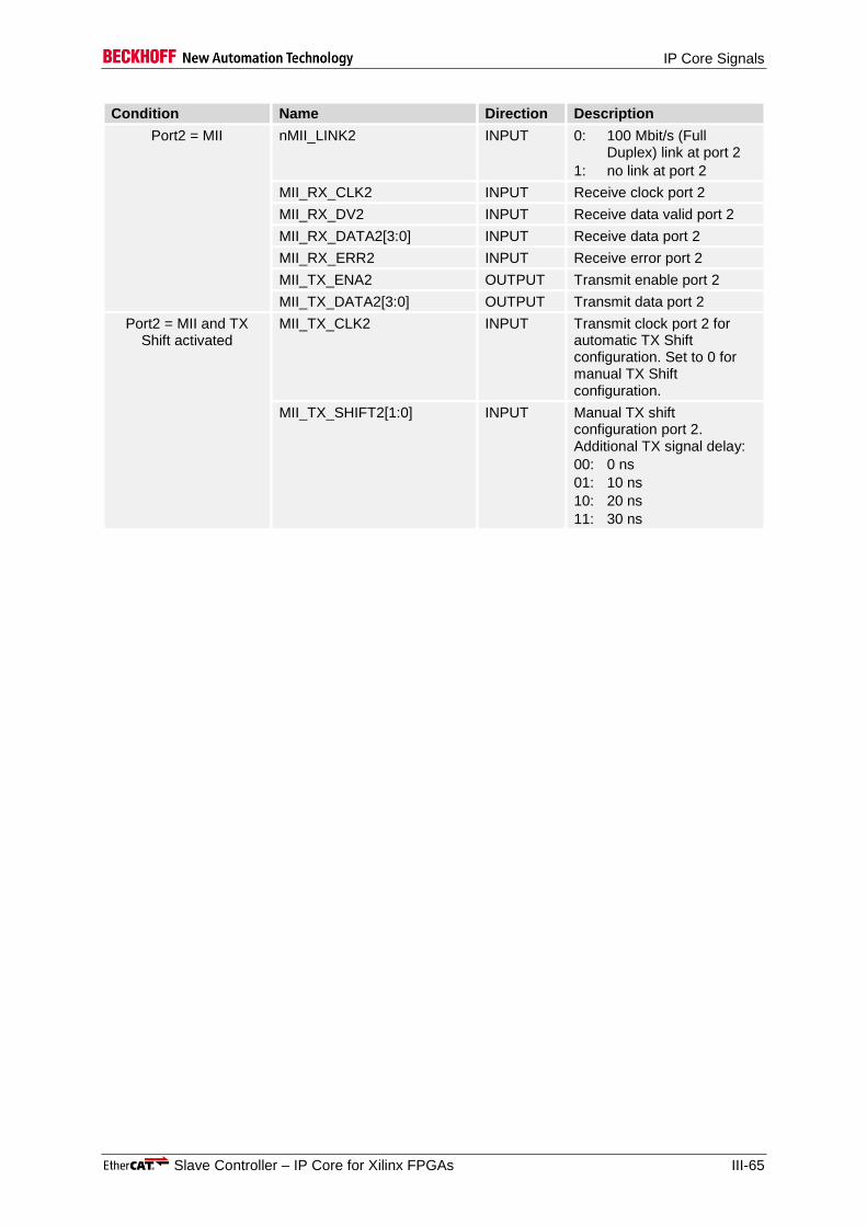
IP Core Signals
Slave Controller – IP Core for Xilinx FPGAs III-65
Condition Name Direction Description
Port2 = MII nMII_LINK2 INPUT 0: 100 Mbit/s (Full Duplex) link at port 2
1: no link at port 2
MII_RX_CLK2 INPUT Receive clock port 2
MII_RX_DV2 INPUT Receive data valid port 2
MII_RX_DATA2[3:0] INPUT Receive data port 2
MII_RX_ERR2 INPUT Receive error port 2
MII_TX_ENA2 OUTPUT Transmit enable port 2
MII_TX_DATA2[3:0] OUTPUT Transmit data port 2
Port2 = MII and TX Shift activated
MII_TX_CLK2 INPUT Transmit clock port 2 for automatic TX Shift configuration. Set to 0 for manual TX Shift configuration.
MII_TX_SHIFT2[1:0] INPUT Manual TX shift configuration port 2. Additional TX signal delay:
00: 0 ns
01: 10 ns
10: 20 ns
11: 30 ns

IP Core Signals
III-66 Slave Controller – IP Core for Xilinx FPGAs
8.5.2 RMII Interface
Table 24 lists the signals used with RMII.
Table 24: PHY Interface RMII
Condition Name Direction Description
Selected communication
interface Port0/Port1 = RMII
CLK50 INPUT
50 MHz reference clock signal from PLL (rising edge synchronous with rising edge of CLK100), also connected to PHY
nRMII_LINK0 INPUT
0: 100 Mbit/s (Full Duplex) link at port 0
1: no link at port 0
RMII_RX_DV0 INPUT Carrier sense/receive data valid port 0
RMII_RX_DATA0[1:0] INPUT Receive data port 0
RMII_RX_ERR0 INPUT Receive error port 0
RMII_TX_ENA0 OUTPUT Transmit enable port 0
RMII_TX_DATA0[1:0] OUTPUT Transmit data port 0
2 communication ports and
selected communication
interface Port1 = RMII
nRMII_LINK1 INPUT
0: 100 Mbit/s (Full Duplex) link at port 1
1: no link at port 1
RMII_RX_DV1 INPUT Carrier sense/receive data valid port 1
RMII_RX_DATA1[1:0] INPUT Receive data port 1
RMII_RX_ERR1 INPUT Receive error port 1
RMII_TX_ENA1 OUTPUT Transmit enable port 1
RMII_TX_DATA1[1:0] OUTPUT Transmit data port 1

IP Core Signals
Slave Controller – IP Core for Xilinx FPGAs III-67
8.5.3 RGMII Interface
Table 25 lists the signals used with RGMII.
Table 25: PHY Interface RGMII
Condition Name Direction Description
Port0 = RGMII
CLK25_2NS INPUT 25 MHz clock signal from PLL (rising edge 2 ns after rising edge of CLK25), used for RGMII GTX_CLK
nRGMII_LINK0 INPUT 0: 100 Mbit/s (Full Duplex) link at port 0
1: no link at port 0
RGMII_RX_CLK0 INPUT Receive clock port 0
RGMII_RX_CTL_DATA_DDR_CLK0 OUTPUT
Receive control/data DDR input clock port 0
RGMII_RX_CTL_DATA_DDR_NRESET0 OUTPUT
Receive control/data DDR input reset (act. low) port 0
RGMII_RX_CTL_DDR_L0 INPUT Receive control DDR input low port 0
RGMII_RX_CTL_DDR_H0 INPUT Receive control DDR input high port 0
RGMII_RX_DATA_DDR_L0 INPUT Receive data DDR input low port 0
RGMII_RX_DATA_DDR_H0 INPUT Receive data DDR input high port 0
RGMII_TX_CLK_DDR_CLK0 OUTPUT Transmit clock DDR output clock port 0
RGMII_TX_CLK_DDR_NRESET0 OUTPUT Transmit clock DDR output reset (port 0, act. low)
RGMII_TX_CLK_DDR_L0 OUTPUT Transmit clock DDR output low port 0
RGMII_TX_CLK_DDR_H0 OUTPUT Transmit clock DDR output high port 0
RGMII_TX_CTL_DATA_DDR_CLK0 OUTPUT Transmit control/data DDR output clock port 0
RGMII_TX_CTL_DATA_DDR_NRESET0 OUTPUT Transmit control/data DDR output reset (port 0, act. low)
RGMII_TX_CTL_DDR_L0 OUTPUT Transmit control DDR output low port 0
RGMII_TX_CTL_DDR_H0 OUTPUT Transmit control DDR output high port 0
RGMII_TX_DATA_DDR_L0 OUTPUT Transmit data DDR output low port 0
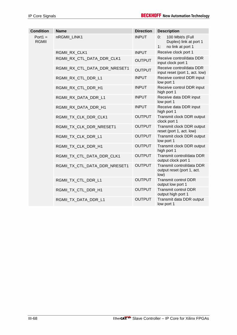
IP Core Signals
III-68 Slave Controller – IP Core for Xilinx FPGAs
Condition Name Direction Description
Port1 = RGMII
nRGMII_LINK1 INPUT 0: 100 Mbit/s (Full Duplex) link at port 1
1: no link at port 1
RGMII_RX_CLK1 INPUT Receive clock port 1
RGMII_RX_CTL_DATA_DDR_CLK1 OUTPUT
Receive control/data DDR input clock port 1
RGMII_RX_CTL_DATA_DDR_NRESET1 OUTPUT
Receive control/data DDR input reset (port 1, act. low)
RGMII_RX_CTL_DDR_L1 INPUT Receive control DDR input low port 1
RGMII_RX_CTL_DDR_H1 INPUT Receive control DDR input high port 1
RGMII_RX_DATA_DDR_L1 INPUT Receive data DDR input low port 1
RGMII_RX_DATA_DDR_H1 INPUT Receive data DDR input high port 1
RGMII_TX_CLK_DDR_CLK1 OUTPUT Transmit clock DDR output clock port 1
RGMII_TX_CLK_DDR_NRESET1 OUTPUT Transmit clock DDR output reset (port 1, act. low)
RGMII_TX_CLK_DDR_L1 OUTPUT Transmit clock DDR output low port 1
RGMII_TX_CLK_DDR_H1 OUTPUT Transmit clock DDR output high port 1
RGMII_TX_CTL_DATA_DDR_CLK1 OUTPUT Transmit control/data DDR output clock port 1
RGMII_TX_CTL_DATA_DDR_NRESET1 OUTPUT Transmit control/data DDR output reset (port 1, act. low)
RGMII_TX_CTL_DDR_L1 OUTPUT Transmit control DDR output low port 1
RGMII_TX_CTL_DDR_H1 OUTPUT Transmit control DDR output high port 1
RGMII_TX_DATA_DDR_L1 OUTPUT Transmit data DDR output low port 1
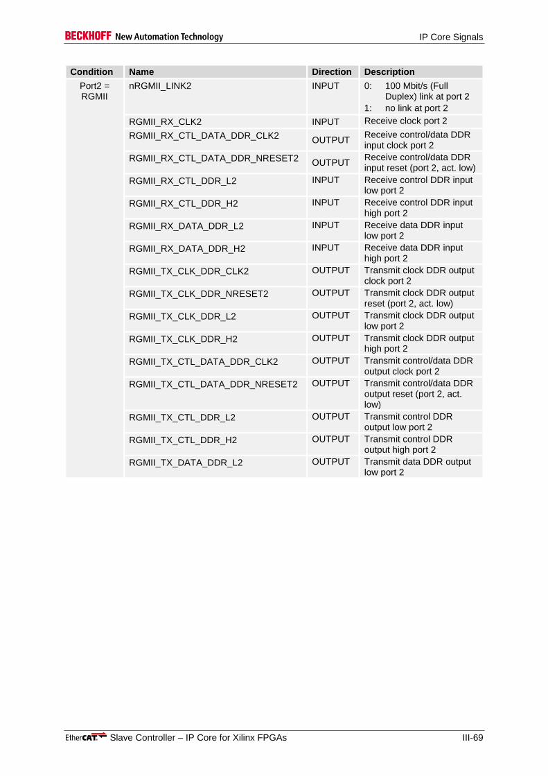
IP Core Signals
Slave Controller – IP Core for Xilinx FPGAs III-69
Condition Name Direction Description
Port2 = RGMII
nRGMII_LINK2 INPUT 0: 100 Mbit/s (Full Duplex) link at port 2
1: no link at port 2
RGMII_RX_CLK2 INPUT Receive clock port 2
RGMII_RX_CTL_DATA_DDR_CLK2 OUTPUT
Receive control/data DDR input clock port 2
RGMII_RX_CTL_DATA_DDR_NRESET2 OUTPUT
Receive control/data DDR input reset (port 2, act. low)
RGMII_RX_CTL_DDR_L2 INPUT Receive control DDR input low port 2
RGMII_RX_CTL_DDR_H2 INPUT Receive control DDR input high port 2
RGMII_RX_DATA_DDR_L2 INPUT Receive data DDR input low port 2
RGMII_RX_DATA_DDR_H2 INPUT Receive data DDR input high port 2
RGMII_TX_CLK_DDR_CLK2 OUTPUT Transmit clock DDR output clock port 2
RGMII_TX_CLK_DDR_NRESET2 OUTPUT Transmit clock DDR output reset (port 2, act. low)
RGMII_TX_CLK_DDR_L2 OUTPUT Transmit clock DDR output low port 2
RGMII_TX_CLK_DDR_H2 OUTPUT Transmit clock DDR output high port 2
RGMII_TX_CTL_DATA_DDR_CLK2 OUTPUT Transmit control/data DDR output clock port 2
RGMII_TX_CTL_DATA_DDR_NRESET2 OUTPUT Transmit control/data DDR output reset (port 2, act. low)
RGMII_TX_CTL_DDR_L2 OUTPUT Transmit control DDR output low port 2
RGMII_TX_CTL_DDR_H2 OUTPUT Transmit control DDR output high port 2
RGMII_TX_DATA_DDR_L2 OUTPUT Transmit data DDR output low port 2
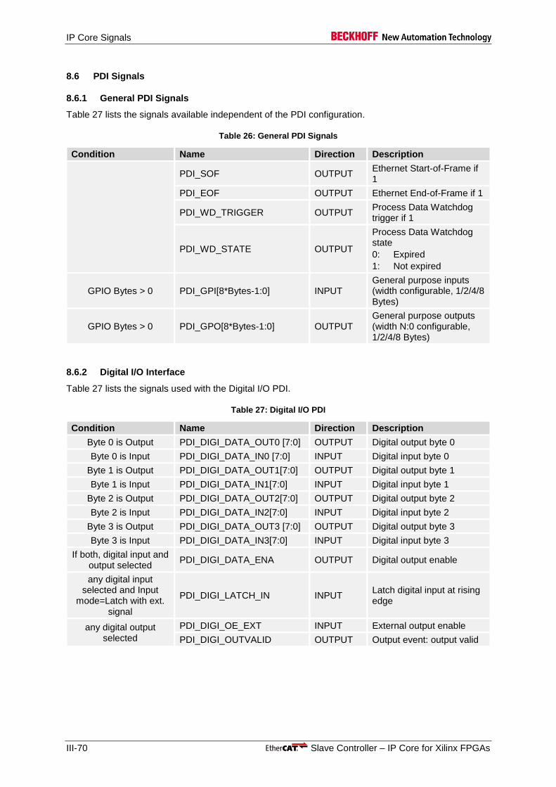
IP Core Signals
III-70 Slave Controller – IP Core for Xilinx FPGAs
8.6 PDI Signals
8.6.1 General PDI Signals
Table 27 lists the signals available independent of the PDI configuration.
Table 26: General PDI Signals
Condition Name Direction Description
PDI_SOF OUTPUT Ethernet Start-of-Frame if 1
PDI_EOF OUTPUT Ethernet End-of-Frame if 1
PDI_WD_TRIGGER OUTPUT Process Data Watchdog trigger if 1
PDI_WD_STATE OUTPUT
Process Data Watchdog state
0: Expired
1: Not expired
GPIO Bytes > 0 PDI_GPI[8*Bytes-1:0] INPUT General purpose inputs (width configurable, 1/2/4/8 Bytes)
GPIO Bytes > 0 PDI_GPO[8*Bytes-1:0] OUTPUT General purpose outputs (width N:0 configurable, 1/2/4/8 Bytes)
8.6.2 Digital I/O Interface
Table 27 lists the signals used with the Digital I/O PDI.
Table 27: Digital I/O PDI
Condition Name Direction Description
Byte 0 is Output PDI_DIGI_DATA_OUT0 [7:0] OUTPUT Digital output byte 0
Byte 0 is Input PDI_DIGI_DATA_IN0 [7:0] INPUT Digital input byte 0
Byte 1 is Output PDI_DIGI_DATA_OUT1[7:0] OUTPUT Digital output byte 1
Byte 1 is Input PDI_DIGI_DATA_IN1[7:0] INPUT Digital input byte 1
Byte 2 is Output PDI_DIGI_DATA_OUT2[7:0] OUTPUT Digital output byte 2
Byte 2 is Input PDI_DIGI_DATA_IN2[7:0] INPUT Digital input byte 2
Byte 3 is Output PDI_DIGI_DATA_OUT3 [7:0] OUTPUT Digital output byte 3
Byte 3 is Input PDI_DIGI_DATA_IN3[7:0] INPUT Digital input byte 3
If both, digital input and output selected
PDI_DIGI_DATA_ENA OUTPUT Digital output enable
any digital input selected and Input
mode=Latch with ext. signal
PDI_DIGI_LATCH_IN INPUT Latch digital input at rising edge
any digital output selected
PDI_DIGI_OE_EXT INPUT External output enable
PDI_DIGI_OUTVALID OUTPUT Output event: output valid
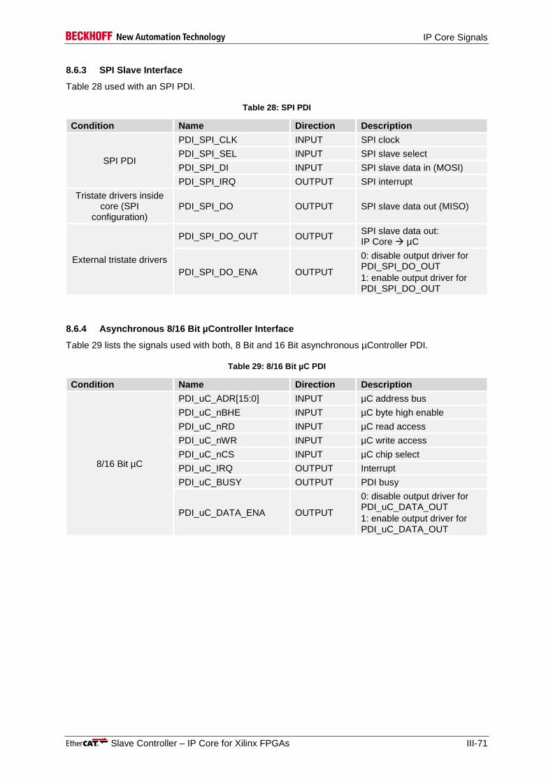
IP Core Signals
Slave Controller – IP Core for Xilinx FPGAs III-71
8.6.3 SPI Slave Interface
Table 28 used with an SPI PDI.
Table 28: SPI PDI
Condition Name Direction Description
SPI PDI
PDI_SPI_CLK INPUT SPI clock
PDI_SPI_SEL INPUT SPI slave select
PDI_SPI_DI INPUT SPI slave data in (MOSI)
PDI_SPI_IRQ OUTPUT SPI interrupt
Tristate drivers inside core (SPI
configuration) PDI_SPI_DO OUTPUT SPI slave data out (MISO)
External tristate drivers
PDI_SPI_DO_OUT OUTPUT SPI slave data out: IP Core µC
PDI_SPI_DO_ENA OUTPUT
0: disable output driver for PDI_SPI_DO_OUT
1: enable output driver for PDI_SPI_DO_OUT
8.6.4 Asynchronous 8/16 Bit µController Interface
Table 29 lists the signals used with both, 8 Bit and 16 Bit asynchronous µController PDI.
Table 29: 8/16 Bit µC PDI
Condition Name Direction Description
8/16 Bit µC
PDI_uC_ADR[15:0] INPUT µC address bus
PDI_uC_nBHE INPUT µC byte high enable
PDI_uC_nRD INPUT µC read access
PDI_uC_nWR INPUT µC write access
PDI_uC_nCS INPUT µC chip select
PDI_uC_IRQ OUTPUT Interrupt
PDI_uC_BUSY OUTPUT PDI busy
PDI_uC_DATA_ENA OUTPUT
0: disable output driver for PDI_uC_DATA_OUT
1: enable output driver for PDI_uC_DATA_OUT
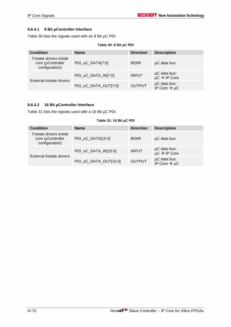
IP Core Signals
III-72 Slave Controller – IP Core for Xilinx FPGAs
8.6.4.1 8 Bit µController Interface
Table 30 lists the signals used with an 8 Bit µC PDI.
Table 30: 8 Bit µC PDI
Condition Name Direction Description
Tristate drivers inside core (µController
configuration) PDI_uC_DATA[7:0] BIDIR µC data bus
External tristate drivers
PDI_uC_DATA_IN[7:0] INPUT µC data bus: µC IP Core
PDI_uC_DATA_OUT[7:0] OUTPUT µC data bus : IP Core µC
8.6.4.2 16 Bit µController Interface
Table 31 lists the signals used with a 16 Bit µC PDI.
Table 31: 16 Bit µC PDI
Condition Name Direction Description
Tristate drivers inside core (µController
configuration) PDI_uC_DATA[15:0] BIDIR µC data bus
External tristate drivers
PDI_uC_DATA_IN[15:0] INPUT µC data bus: µC IP Core
PDI_uC_DATA_OUT[15:0] OUTPUT µC data bus: IP Core µC
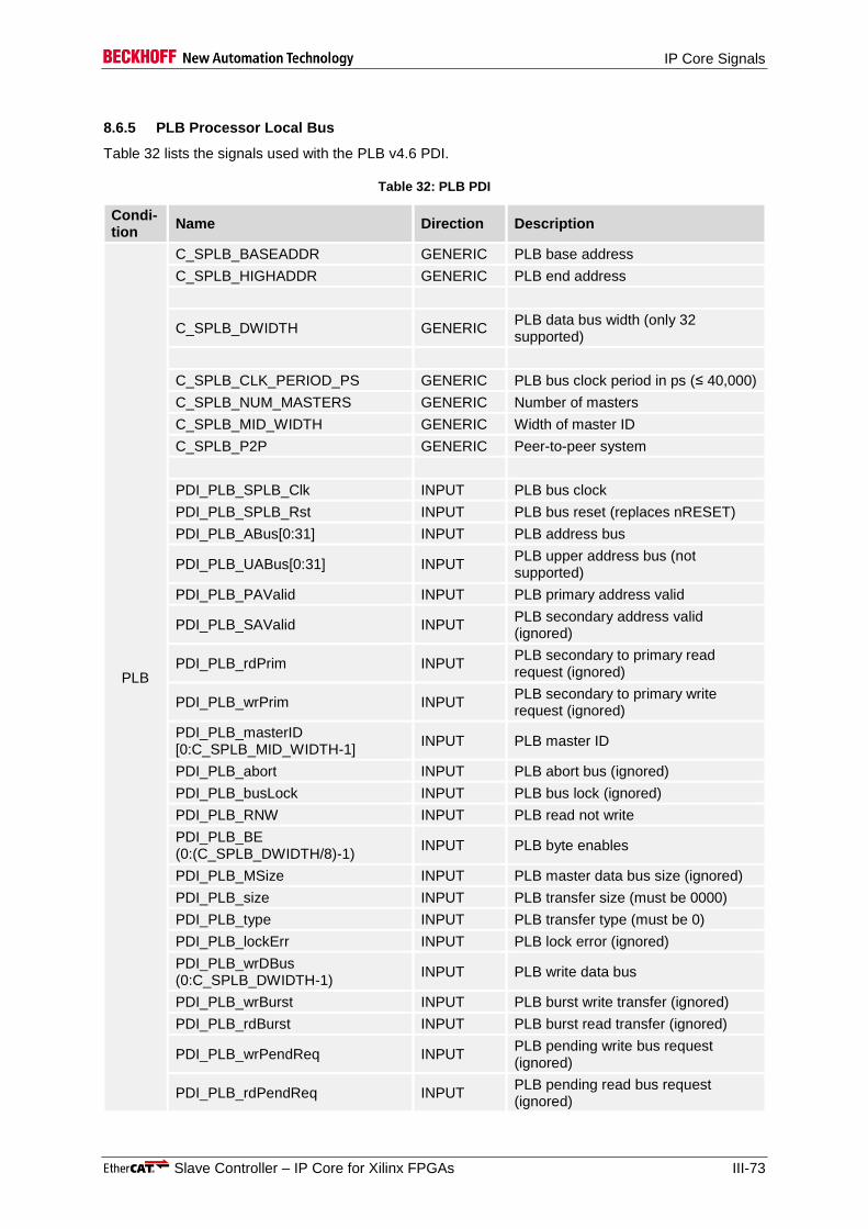
IP Core Signals
Slave Controller – IP Core for Xilinx FPGAs III-73
8.6.5 PLB Processor Local Bus
Table 32 lists the signals used with the PLB v4.6 PDI.
Table 32: PLB PDI
Condi-tion
Name Direction Description
PLB
C_SPLB_BASEADDR GENERIC PLB base address
C_SPLB_HIGHADDR GENERIC PLB end address
C_SPLB_DWIDTH GENERIC PLB data bus width (only 32 supported)
C_SPLB_CLK_PERIOD_PS GENERIC PLB bus clock period in ps (≤ 40,000)
C_SPLB_NUM_MASTERS GENERIC Number of masters
C_SPLB_MID_WIDTH GENERIC Width of master ID
C_SPLB_P2P GENERIC Peer-to-peer system
PDI_PLB_SPLB_Clk INPUT PLB bus clock
PDI_PLB_SPLB_Rst INPUT PLB bus reset (replaces nRESET)
PDI_PLB_ABus[0:31] INPUT PLB address bus
PDI_PLB_UABus[0:31] INPUT PLB upper address bus (not supported)
PDI_PLB_PAValid INPUT PLB primary address valid
PDI_PLB_SAValid INPUT PLB secondary address valid (ignored)
PDI_PLB_rdPrim INPUT PLB secondary to primary read request (ignored)
PDI_PLB_wrPrim INPUT PLB secondary to primary write request (ignored)
PDI_PLB_masterID [0:C_SPLB_MID_WIDTH-1]
INPUT PLB master ID
PDI_PLB_abort INPUT PLB abort bus (ignored)
PDI_PLB_busLock INPUT PLB bus lock (ignored)
PDI_PLB_RNW INPUT PLB read not write
PDI_PLB_BE (0:(C_SPLB_DWIDTH/8)-1)
INPUT PLB byte enables
PDI_PLB_MSize INPUT PLB master data bus size (ignored)
PDI_PLB_size INPUT PLB transfer size (must be 0000)
PDI_PLB_type INPUT PLB transfer type (must be 0)
PDI_PLB_lockErr INPUT PLB lock error (ignored)
PDI_PLB_wrDBus (0:C_SPLB_DWIDTH-1)
INPUT PLB write data bus
PDI_PLB_wrBurst INPUT PLB burst write transfer (ignored)
PDI_PLB_rdBurst INPUT PLB burst read transfer (ignored)
PDI_PLB_wrPendReq INPUT PLB pending write bus request (ignored)
PDI_PLB_rdPendReq INPUT PLB pending read bus request (ignored)
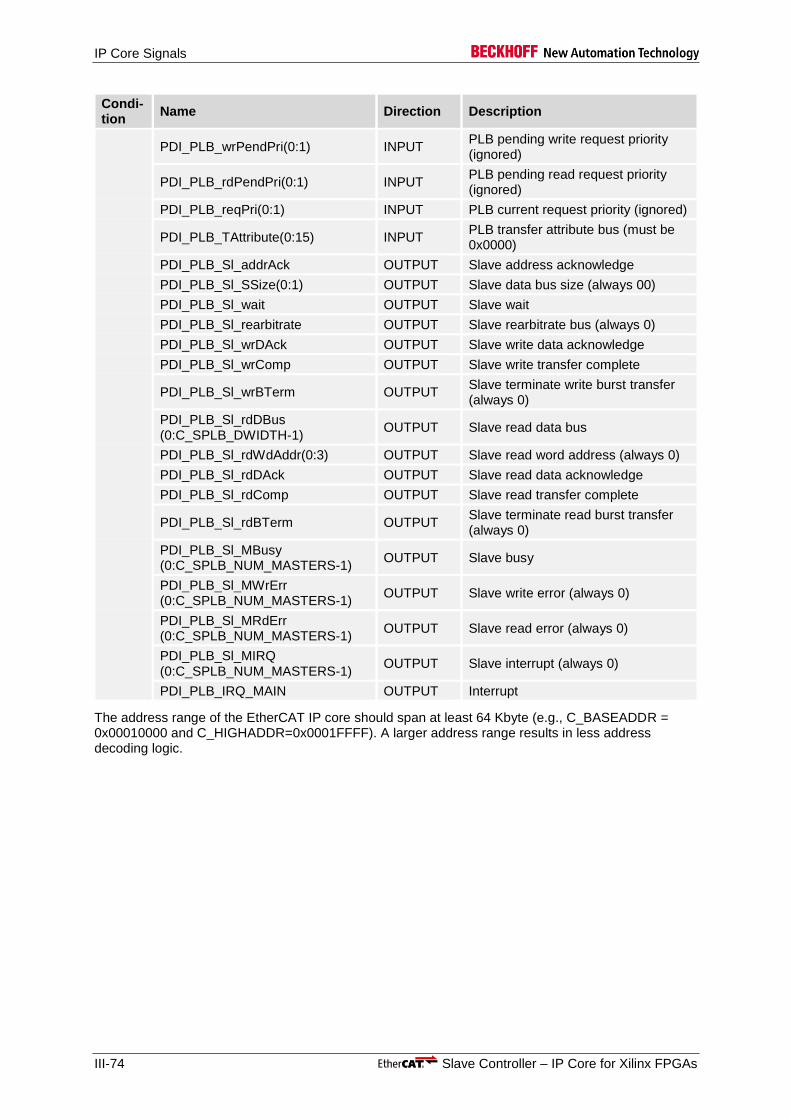
IP Core Signals
III-74 Slave Controller – IP Core for Xilinx FPGAs
Condi-tion
Name Direction Description
PDI_PLB_wrPendPri(0:1) INPUT PLB pending write request priority (ignored)
PDI_PLB_rdPendPri(0:1) INPUT PLB pending read request priority (ignored)
PDI_PLB_reqPri(0:1) INPUT PLB current request priority (ignored)
PDI_PLB_TAttribute(0:15) INPUT PLB transfer attribute bus (must be 0x0000)
PDI_PLB_Sl_addrAck OUTPUT Slave address acknowledge
PDI_PLB_Sl_SSize(0:1) OUTPUT Slave data bus size (always 00)
PDI_PLB_Sl_wait OUTPUT Slave wait
PDI_PLB_Sl_rearbitrate OUTPUT Slave rearbitrate bus (always 0)
PDI_PLB_Sl_wrDAck OUTPUT Slave write data acknowledge
PDI_PLB_Sl_wrComp OUTPUT Slave write transfer complete
PDI_PLB_Sl_wrBTerm OUTPUT Slave terminate write burst transfer (always 0)
PDI_PLB_Sl_rdDBus (0:C_SPLB_DWIDTH-1)
OUTPUT Slave read data bus
PDI_PLB_Sl_rdWdAddr(0:3) OUTPUT Slave read word address (always 0)
PDI_PLB_Sl_rdDAck OUTPUT Slave read data acknowledge
PDI_PLB_Sl_rdComp OUTPUT Slave read transfer complete
PDI_PLB_Sl_rdBTerm OUTPUT Slave terminate read burst transfer (always 0)
PDI_PLB_Sl_MBusy (0:C_SPLB_NUM_MASTERS-1)
OUTPUT Slave busy
PDI_PLB_Sl_MWrErr (0:C_SPLB_NUM_MASTERS-1)
OUTPUT Slave write error (always 0)
PDI_PLB_Sl_MRdErr (0:C_SPLB_NUM_MASTERS-1)
OUTPUT Slave read error (always 0)
PDI_PLB_Sl_MIRQ (0:C_SPLB_NUM_MASTERS-1)
OUTPUT Slave interrupt (always 0)
PDI_PLB_IRQ_MAIN OUTPUT Interrupt
The address range of the EtherCAT IP core should span at least 64 Kbyte (e.g., C_BASEADDR = 0x00010000 and C_HIGHADDR=0x0001FFFF). A larger address range results in less address decoding logic.
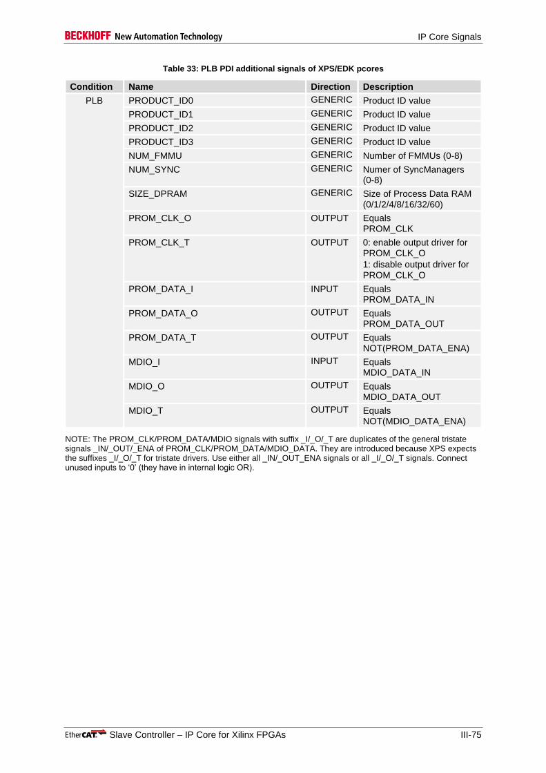
IP Core Signals
Slave Controller – IP Core for Xilinx FPGAs III-75
Table 33: PLB PDI additional signals of XPS/EDK pcores
Condition Name Direction Description
PLB PRODUCT_ID0 GENERIC Product ID value
PRODUCT_ID1 GENERIC Product ID value
PRODUCT_ID2 GENERIC Product ID value
PRODUCT_ID3 GENERIC Product ID value
NUM_FMMU GENERIC Number of FMMUs (0-8)
NUM_SYNC GENERIC Numer of SyncManagers (0-8)
SIZE_DPRAM GENERIC Size of Process Data RAM (0/1/2/4/8/16/32/60)
PROM_CLK_O OUTPUT Equals PROM_CLK
PROM_CLK_T OUTPUT 0: enable output driver for PROM_CLK_O
1: disable output driver for PROM_CLK_O
PROM_DATA_I INPUT Equals PROM_DATA_IN
PROM_DATA_O OUTPUT Equals PROM_DATA_OUT
PROM_DATA_T OUTPUT Equals NOT(PROM_DATA_ENA)
MDIO_I INPUT Equals MDIO_DATA_IN
MDIO_O OUTPUT Equals MDIO_DATA_OUT
MDIO_T OUTPUT Equals NOT(MDIO_DATA_ENA)
NOTE: The PROM_CLK/PROM_DATA/MDIO signals with suffix _I/_O/_T are duplicates of the general tristate signals _IN/_OUT/_ENA of PROM_CLK/PROM_DATA/MDIO_DATA. They are introduced because XPS expects the suffixes _I/_O/_T for tristate drivers. Use either all _IN/_OUT_ENA signals or all _I/_O/_T signals. Connect unused inputs to ‘0’ (they have in internal logic OR).

IP Core Signals
III-76 Slave Controller – IP Core for Xilinx FPGAs
8.6.6 AXI4 / AXI4 LITE On-Chip Bus
Table 34 lists the signals used with the AXI4 and AXI4 LITE PDI.
Table 34: AXI4 / AXI4 LITE PDI
Condition Name Direction Description
AXI4 or
AXI4 LITE
C_S_AXI_DATA_WIDTH GENERIC AXI data bus width (8/16/32/64 bit)
C_S_AXI_ACLK_FREQ_HZ GENERIC AXI bus clock frequency in Hz (>= 25,000)
C_S_AXI_ADDR_WIDTH GENERIC AXI address width (>= 16 bit, only 16 bit are used)
C_S_AXI_ID_WIDTH GENERIC AXI ID width
PDI_AXI_ACLK INPUT AXI bus clock
PDI_AXI_AWADDR[15:0] INPUT Write address
PDI_AXI_AWPROT[2:0] INPUT Write protection type
PDI_AXI_AWREGION[3:0] INPUT Write region identifier
PDI_AXI_AWQOS[3:0] INPUT Write QoS identifier
PDI_AXI_AWVALID INPUT Write address valid
PDI_AXI_AWREADY OUTPUT Write address ready
PDI_AXI_WDATA [PDI_EXT_BUS_WIDTH-1:0]
INPUT Write data
PDI_AXI_WSTRB [PDI_EXT_BUS_WIDTH/8-1:0]
INPUT Write data byte enable
PDI_AXI_WVALID INPUT Write data valid
PDI_AXI_WREADY OUTPUT Write data ready
PDI_AXI_BRESP[1:0] OUTPUT Write response
PDI_AXI_BVALID OUTPUT Write response valid
PDI_AXI_BREADY INPUT Write response ready
PDI_AXI_ARADDR[15:0] INPUT Read address
PDI_AXI_ARPROT[2:0] INPUT Read protection type
PDI_AXI_ARREGION[3:0] INPUT Read region identifier
PDI_AXI_ARQOS[3:0] INPUT Read QoS identifier
PDI_AXI_ARVALID INPUT Read address valid
PDI_AXI_ARREADY OUTPUT Read address ready
PDI_AXI_RDATA [PDI_EXT_BUS_WIDTH-1:0]
OUTPUT Read data
PDI_AXI_RRESP[1:0] OUTPUT Read response
PDI_AXI_RVALID OUTPUT Read data valid
PDI_AXI_RREADY INPUT Read data ready
PDI_AXI_IRQ_MAIN OUTPUT Interrupt
PDI_AXI_AWID [PDI_BUS_ID_WIDTH-1:0]
INPUT Write address ID
PDI_AXI_AWLEN[7:0] INPUT Write length
PDI_AXI_AWSIZE[2:0] INPUT Write size
PDI_AXI_AWBURST[1:0] INPUT Write burst type
PDI_AXI_AWLOCK INPUT Write lock
PDI_AXI_AWCACHE[3:0] INPUT Write cache type
PDI_AXI_WLAST INPUT Write data last

IP Core Signals
Slave Controller – IP Core for Xilinx FPGAs III-77
Condition Name Direction Description
AXI4 PDI_AXI_BID[PDI_BUS_ID_WIDTH-1:0] OUTPUT Write response ID
PDI_AXI_ARID[PDI_BUS_ID_WIDTH-1:0] INPUT Read address ID
PDI_AXI_ARLEN[7:0] INPUT Read length
PDI_AXI_ARSIZE[2:0] INPUT Read size
PDI_AXI_ARBURST[1:0] INPUT Read burst type
PDI_AXI_ARLOCK INPUT Read lock
PDI_AXI_ARCACHE[3:0] INPUT Read cache type
PDI_AXI_RID [PDI_BUS_ID_WIDTH-1:0]
OUTPUT Read data ID
PDI_AXI_RLAST OUTPUT Read data last
Table 35: AXI4 / AXI4 LITE PDI additional signals of XPS/EDK pcores
Condition Name Direction Description
AXI4 or
AXI4 LITE
PRODUCT_ID0 GENERIC Product ID value
PRODUCT_ID1 GENERIC Product ID value
PRODUCT_ID2 GENERIC Product ID value
PRODUCT_ID3 GENERIC Product ID value
NUM_FMMU GENERIC Number of FMMUs (0-8)
NUM_SYNC GENERIC Numer of SyncManagers (0-8)
SIZE_DPRAM GENERIC Size of Process Data RAM (0/1/2/4/8/16/32/60)
C_S_AXI_BASEADDR GENERIC Unused AXI base address
C_S_AXI_HIGHADDR GENERIC Unused AXI high address
PROM_CLK_O OUTPUT Equals PROM_CLK
PROM_CLK_T OUTPUT 0: enable output driver for PROM_CLK_O
1: disable output driver for PROM_CLK_O
PROM_DATA_I INPUT Equals PROM_DATA_IN
PROM_DATA_O OUTPUT Equals PROM_DATA_OUT
PROM_DATA_T OUTPUT Equals NOT(PROM_DATA_ENA)
MDIO_I INPUT Equals MDIO_DATA_IN
MDIO_O OUTPUT Equals MDIO_DATA_OUT
MDIO_T OUTPUT Equals NOT(MDIO_DATA_ENA)
NOTE: The PROM_CLK/PROM_DATA/MDIO signals with suffix _I/_O/_T are duplicates of the general tristate signals _IN/_OUT/_ENA of PROM_CLK/PROM_DATA/MDIO_DATA. They are introduced because XPS expects the suffixes _I/_O/_T for tristate drivers. Use either all _IN/_OUT_ENA signals or all _I/_O/_T signals. Connect unused inputs to ‘0’ (they have in internal logic OR).
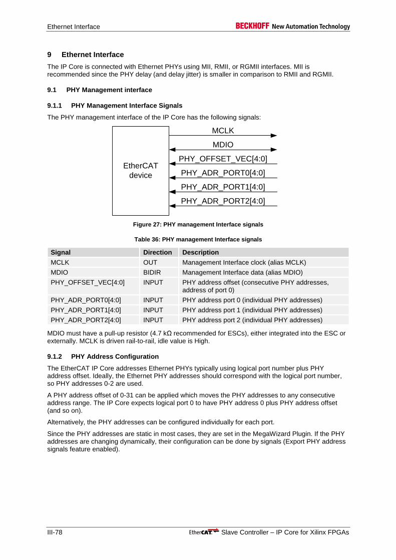
Ethernet Interface
III-78 Slave Controller – IP Core for Xilinx FPGAs
9 Ethernet Interface
The IP Core is connected with Ethernet PHYs using MII, RMII, or RGMII interfaces. MII is recommended since the PHY delay (and delay jitter) is smaller in comparison to RMII and RGMII.
9.1 PHY Management interface
9.1.1 PHY Management Interface Signals
The PHY management interface of the IP Core has the following signals:
EtherCAT
device
MCLK
MDIO
PHY_OFFSET_VEC[4:0]
PHY_ADR_PORT0[4:0]
PHY_ADR_PORT1[4:0]
PHY_ADR_PORT2[4:0]
Figure 27: PHY management Interface signals
Table 36: PHY management Interface signals
Signal Direction Description
MCLK OUT Management Interface clock (alias MCLK)
MDIO BIDIR Management Interface data (alias MDIO)
PHY_OFFSET_VEC[4:0] INPUT PHY address offset (consecutive PHY addresses, address of port 0)
PHY_ADR_PORT0[4:0] INPUT PHY address port 0 (individual PHY addresses)
PHY_ADR_PORT1[4:0] INPUT PHY address port 1 (individual PHY addresses)
PHY_ADR_PORT2[4:0] INPUT PHY address port 2 (individual PHY addresses)
MDIO must have a pull-up resistor (4.7 kΩ recommended for ESCs), either integrated into the ESC or externally. MCLK is driven rail-to-rail, idle value is High.
9.1.2 PHY Address Configuration
The EtherCAT IP Core addresses Ethernet PHYs typically using logical port number plus PHY address offset. Ideally, the Ethernet PHY addresses should correspond with the logical port number, so PHY addresses 0-2 are used.
A PHY address offset of 0-31 can be applied which moves the PHY addresses to any consecutive address range. The IP Core expects logical port 0 to have PHY address 0 plus PHY address offset (and so on).
Alternatively, the PHY addresses can be configured individually for each port.
Since the PHY addresses are static in most cases, they are set in the MegaWizard Plugin. If the PHY addresses are changing dynamically, their configuration can be done by signals (Export PHY address signals feature enabled).

Ethernet Interface
Slave Controller – IP Core for Xilinx FPGAs III-79
9.1.3 Separate external MII management interfaces
If two separate external MII management interfaces are to be connected to the single MII management interface of the EtherCAT IP Core, some glue logic has to be added. Disable internal Tri-State drivers for the MII management bus and combine the signals according to the following figure. Take care of proper PHY address configuration: the PHYs need different PHY addresses.
EtherCAT IP Core
Ethernet PHY
MDIO_IN
MCLK
MDIO
MDC
4K
7
VCC I/O
Ethernet PHY
MDIO
MDC
4K
7
VCC I/O
MDIO_OUT
MDIO_ENA
&
FPGA
Figure 28: Example schematic with two individual MII management interfaces
9.1.4 MII management timing specifications
For MII Management Interface timing diagrams refer to Section I.
Table 37: MII management timing characteristics
Parameter Min Typ Max Comment
PRELIMINARY TIMING
tMI_startup 1.34 ms Time between nPHY_RESET_OUT reset end and the first access via management interface
tClk 400 ns MI_CLK period
tWrite ~ 25.6 µs MI Write access time
tRead ~ 25.4 µs MI Read access time
Ethernet Interface
III-80 Slave Controller – IP Core for Xilinx FPGAs
9.2 MII Interface
The MII interface of the IP Core is optimized for low processing/forwarding delays by omitting a transmit FIFO. To allow this, the IP Core has additional requirements to Ethernet PHYs, which are easily accomplished by several PHY vendors.
Refer to “Section I – Technology” for Ethernet PHY requirements.
Additional information regarding the IP Core:
The clock source of the PHYs is the same as for the FPGA (25 MHz quartz oscillator)
The signal polarity of nMII_LINK is not configurable inside the IP Core, nMII_LINK is active low. If necessary, the signal polarity must be swapped by user logic outside the IP Core.
The IP Core can be configured to use the MII management interface for link detection and link configuration.
The IP Core supports arbitrary PHY addresses
For details about the ESC MII Interface refer to Section I.

Ethernet Interface
Slave Controller – IP Core for Xilinx FPGAs III-81
9.2.1 MII Interface Signals
The MII interface of the IP Core has the following signals:
EtherCAT
device
MII_RX_CLK
nMII_LINK
MII_RX_DV
MII_RX_ERR
MII_RX_DATA[3:0]
MII_TX_ENA
MII_TX_DATA[3:0]
MII_TX_CLK
MII_TX_SHIFT[1:0]
NPHY_RESET_OUT
Figure 29: MII Interface signals
Table 38: MII Interface signals
Signal Direction Description
nMII_LINK IN Input signal provided by the PHY if a 100 Mbit/s (Full Duplex) link is established (alias LINK_MII)
MII_RX_CLK IN Receive Clock
MII_RX_DV IN Receive data valid
MII_RX_DATA[3:0] IN Receive data (alias RXD)
MII_RX_ERR IN Receive error (alias RX_ER)
MII_TX_ENA OUT Transmit enable (alias TX_EN)
MII_TX_DATA[3:0] OUT Transmit data (alias TXD)
MII_TX_CLK IN Transmit Clock for automatic TX Shift compensation
MII_TX_SHIFT[1:0] IN Manual TX Shift compensation with additional registers
NPHY_RESET_OUT OUT PHY reset (akt. low), resets PHY while ESC is in Reset state, and, for FX PHYs, if Enhanced Link Detection detects a lost link
NOTE: A pull-down resistor is typically required for NPHY_RESET_OUT to hold the PHY in reset state while the FPGA is configured, since this pin is floating or even pulled up during that time.
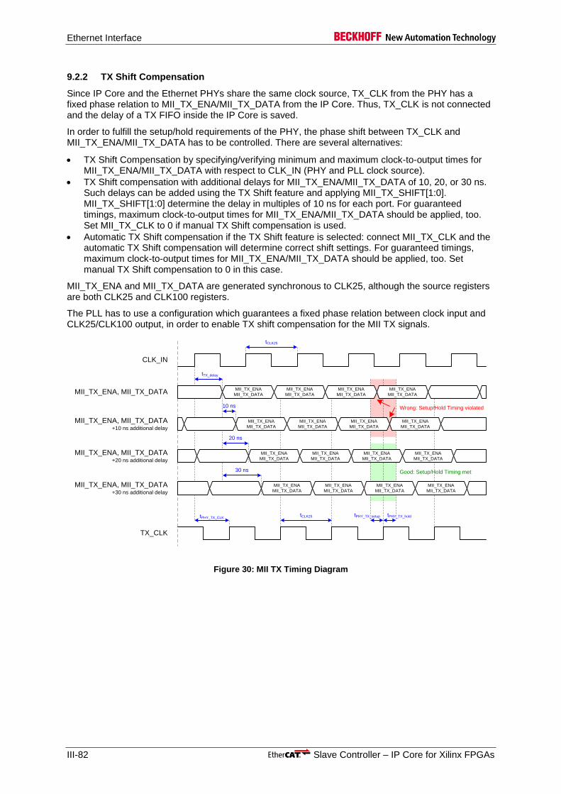
Ethernet Interface
III-82 Slave Controller – IP Core for Xilinx FPGAs
9.2.2 TX Shift Compensation
Since IP Core and the Ethernet PHYs share the same clock source, TX_CLK from the PHY has a fixed phase relation to MII_TX_ENA/MII_TX_DATA from the IP Core. Thus, TX_CLK is not connected and the delay of a TX FIFO inside the IP Core is saved.
In order to fulfill the setup/hold requirements of the PHY, the phase shift between TX_CLK and MII_TX_ENA/MII_TX_DATA has to be controlled. There are several alternatives:
TX Shift Compensation by specifying/verifying minimum and maximum clock-to-output times for MII_TX_ENA/MII_TX_DATA with respect to CLK_IN (PHY and PLL clock source).
TX Shift compensation with additional delays for MII_TX_ENA/MII_TX_DATA of 10, 20, or 30 ns. Such delays can be added using the TX Shift feature and applying MII_TX_SHIFT[1:0]. MII_TX_SHIFT[1:0] determine the delay in multiples of 10 ns for each port. For guaranteed timings, maximum clock-to-output times for MII_TX_ENA/MII_TX_DATA should be applied, too. Set MII_TX_CLK to 0 if manual TX Shift compensation is used.
Automatic TX Shift compensation if the TX Shift feature is selected: connect MII_TX_CLK and the automatic TX Shift compensation will determine correct shift settings. For guaranteed timings, maximum clock-to-output times for MII_TX_ENA/MII_TX_DATA should be applied, too. Set manual TX Shift compensation to 0 in this case.
MII_TX_ENA and MII_TX_DATA are generated synchronous to CLK25, although the source registers are both CLK25 and CLK100 registers.
The PLL has to use a configuration which guarantees a fixed phase relation between clock input and CLK25/CLK100 output, in order to enable TX shift compensation for the MII TX signals.
CLK_IN
TX_CLK
MII_TX_ENA
MII_TX_DATA
MII_TX_ENA
MII_TX_DATA
MII_TX_ENA
MII_TX_DATA
MII_TX_ENA
MII_TX_DATA
MII_TX_ENA
MII_TX_DATA
MII_TX_ENA
MII_TX_DATA
MII_TX_ENA
MII_TX_DATA
MII_TX_ENA
MII_TX_DATA
MII_TX_ENA
MII_TX_DATA
MII_TX_ENA
MII_TX_DATA
MII_TX_ENA
MII_TX_DATA
MII_TX_ENA
MII_TX_DATA
MII_TX_ENA
MII_TX_DATA
MII_TX_ENA
MII_TX_DATA
MII_TX_ENA
MII_TX_DATA
MII_TX_ENA
MII_TX_DATA
tCLK25
10 ns
20 ns
30 ns
tTX_delay
tPHY_TX_holdtPHY_TX_setup
Wrong: Setup/Hold Timing violated
Good: Setup/Hold Timing met
tCLK25tPHY_TX_CLK
MII_TX_ENA, MII_TX_DATA
MII_TX_ENA, MII_TX_DATA+10 ns additional delay
MII_TX_ENA, MII_TX_DATA+20 ns additional delay
MII_TX_ENA, MII_TX_DATA+30 ns additional delay
Figure 30: MII TX Timing Diagram
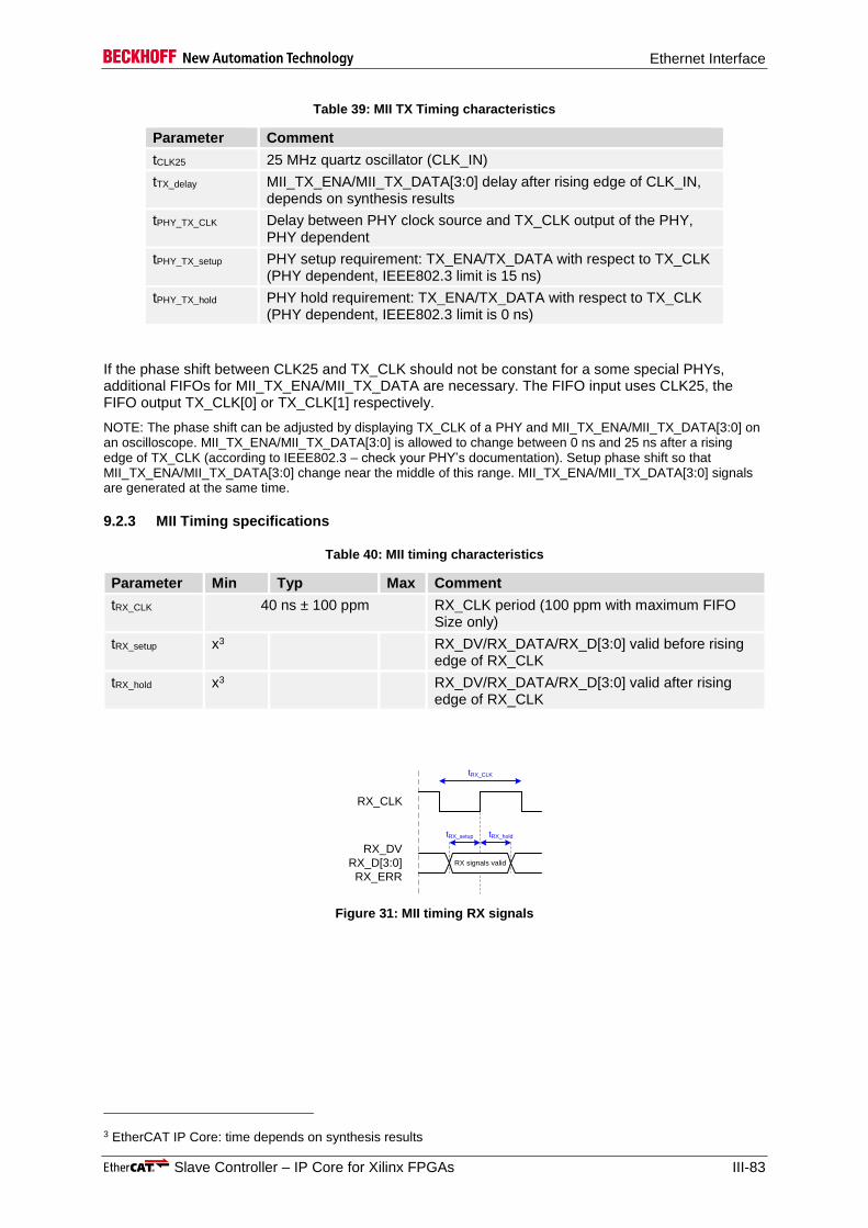
Ethernet Interface
Slave Controller – IP Core for Xilinx FPGAs III-83
Table 39: MII TX Timing characteristics
Parameter Comment
tCLK25 25 MHz quartz oscillator (CLK_IN)
tTX_delay MII_TX_ENA/MII_TX_DATA[3:0] delay after rising edge of CLK_IN, depends on synthesis results
tPHY_TX_CLK Delay between PHY clock source and TX_CLK output of the PHY, PHY dependent
tPHY_TX_setup PHY setup requirement: TX_ENA/TX_DATA with respect to TX_CLK (PHY dependent, IEEE802.3 limit is 15 ns)
tPHY_TX_hold PHY hold requirement: TX_ENA/TX_DATA with respect to TX_CLK (PHY dependent, IEEE802.3 limit is 0 ns)
If the phase shift between CLK25 and TX_CLK should not be constant for a some special PHYs, additional FIFOs for MII_TX_ENA/MII_TX_DATA are necessary. The FIFO input uses CLK25, the FIFO output TX_CLK[0] or TX_CLK[1] respectively.
NOTE: The phase shift can be adjusted by displaying TX_CLK of a PHY and MII_TX_ENA/MII_TX_DATA[3:0] on an oscilloscope. MII_TX_ENA/MII_TX_DATA[3:0] is allowed to change between 0 ns and 25 ns after a rising edge of TX_CLK (according to IEEE802.3 – check your PHY’s documentation). Setup phase shift so that MII_TX_ENA/MII_TX_DATA[3:0] change near the middle of this range. MII_TX_ENA/MII_TX_DATA[3:0] signals are generated at the same time.
9.2.3 MII Timing specifications
Table 40: MII timing characteristics
Parameter Min Typ Max Comment
tRX_CLK 40 ns ± 100 ppm RX_CLK period (100 ppm with maximum FIFO Size only)
tRX_setup x3 RX_DV/RX_DATA/RX_D[3:0] valid before rising edge of RX_CLK
tRX_hold x3 RX_DV/RX_DATA/RX_D[3:0] valid after rising edge of RX_CLK
RX_DV
RX_D[3:0]
RX_ERR
RX_CLK
tRX_setup tRX_hold
RX signals valid
tRX_CLK
Figure 31: MII timing RX signals
3 EtherCAT IP Core: time depends on synthesis results
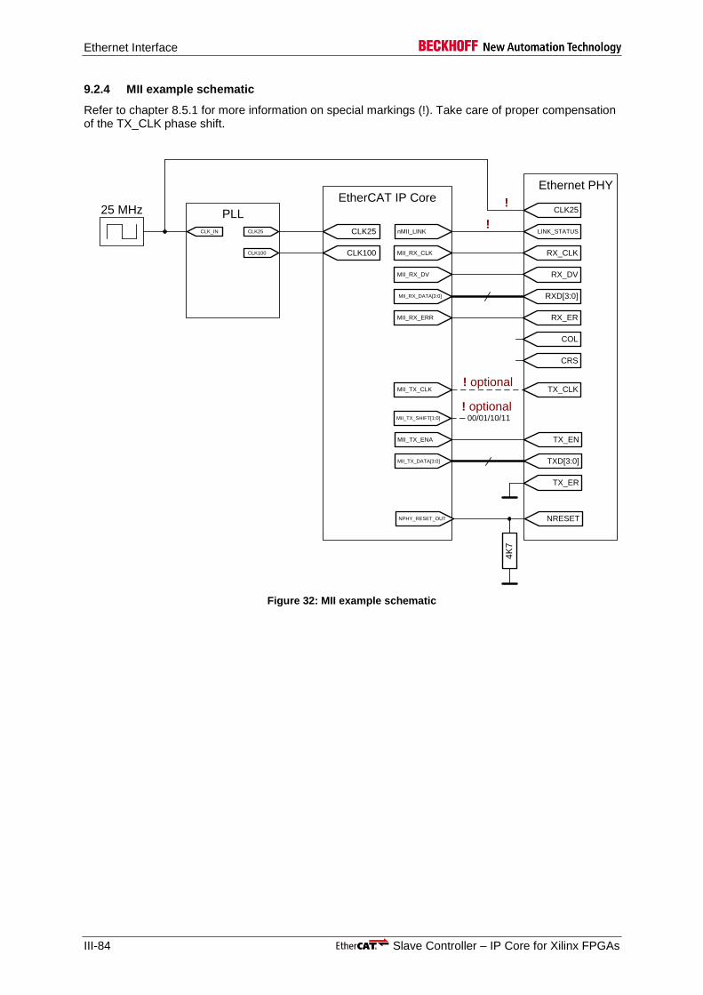
Ethernet Interface
III-84 Slave Controller – IP Core for Xilinx FPGAs
9.2.4 MII example schematic
Refer to chapter 8.5.1 for more information on special markings (!). Take care of proper compensation of the TX_CLK phase shift.
EtherCAT IP CoreEthernet PHY
MII_RX_DV
MII_RX_DATA[3:0]
MII_RX_ERR
MII_TX_ENA
MII_TX_DATA[3:0]
MII_RX_CLK
RX_DV
RXD[3:0]
RX_ER
TX_EN
TXD[3:0]
RX_CLK
TX_CLK
CLK25
CRS
TX_ER
COL
nMII_LINK LINK_STATUS
!
!
! optional
CLK25
PLL
CLK_IN CLK25
CLK100 CLK100
25 MHz
MII_TX_CLK
! optionalMII_TX_SHIFT[1:0] 00/01/10/11
NPHY_RESET_OUT NRESET
4K
7
Figure 32: MII example schematic

Ethernet Interface
Slave Controller – IP Core for Xilinx FPGAs III-85
9.3 RMII Interface
The IP Core supports RMII with 2 communication ports. Nevertheless, MII is recommended since the PHY delay (and delay jitter) is smaller in comparison to RMII.
The Beckhoff ESCs have additional requirements to Ethernet PHYs using RMII, which are easily accomplished by several PHY vendors.
Refer to “Section I – Technology” for Ethernet PHY requirements.
Additional information regarding the IP Core:
The clock source of the PHYs is the same as for the FPGA (25 MHz quartz oscillator)
The signal polarity of nRMII_LINK is not configurable inside the IP Core, nRMII_LINK is active low. If necessary, the signal polarity must be swapped outside the IP Core.
The IP Core can be configured to use the MII management interface for link detection and link configuration.
The IP Core supports arbitrary PHY addresses.
For details about the ESC RMII Interface refer to Section I.
9.3.1 RMII Interface Signals
The RMII interface of the IP Core has the following signals:
EtherCAT
device
nRMII_LINK
CLK50
RMII_RX_DV
RMII_RX_ERR
RMII_RX_DATA[1:0]
RMII_TX_ENA
RMII_TX_DATA[1:0]
NPHY_RESET_OUT
Figure 33: RMII Interface signals
Table 41: RMII Interface signals
Signal Direction Description
CLK50 IN RMII RX/TX reference clock (50 MHz)
nRMII_LINK IN Input signal provided by the PHY if a 100 Mbit/s (Full Duplex) link is established (alias LINK_MII)
RMII_RX_DV IN Carrier sense/receive data valid
RMII_RX_DATA[1:0] IN Receive data (alias RXD)
RMII_RX_ERR IN Receive error (alias RX_ER)
RMII_TX_ENA OUT Transmit enable (alias TX_EN)
RMII_TX_DATA[1:0] OUT Transmit data (alias TXD)
NPHY_RESET_OUT OUT PHY reset (akt. low), resets PHY while ESC is in Reset state, and, for FX PHYs, if Enhanced Link Detection detects a lost link
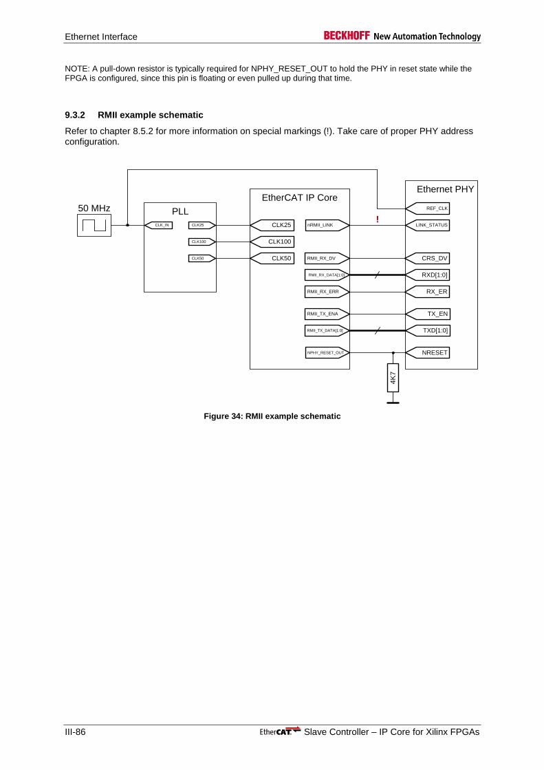
Ethernet Interface
III-86 Slave Controller – IP Core for Xilinx FPGAs
NOTE: A pull-down resistor is typically required for NPHY_RESET_OUT to hold the PHY in reset state while the FPGA is configured, since this pin is floating or even pulled up during that time.
9.3.2 RMII example schematic
Refer to chapter 8.5.2 for more information on special markings (!). Take care of proper PHY address configuration.
EtherCAT IP CoreEthernet PHY
RMII_RX_DV
RMII_RX_DATA[1:0]
RMII_RX_ERR
RMII_TX_ENA
RMII_TX_DATA[1:0]
CRS_DV
RXD[1:0]
RX_ER
TX_EN
TXD[1:0]
REF_CLK
nRMII_LINK LINK_STATUS!
CLK25
PLL
CLK_IN CLK25
CLK100 CLK100
50 MHz
CLK50 CLK50
NPHY_RESET_OUT NRESET
4K
7
Figure 34: RMII example schematic
Ethernet Interface
Slave Controller – IP Core for Xilinx FPGAs III-87
9.4 RGMII Interface
The IP Core supports RGMII with1-3 communication ports at 100 Mbit/s. Nevertheless, MII is recommended since the PHY delay (and delay jitter) is smaller in comparison to RGMII.
The RGMII interface of the EtherCAT IP Core offers signals for attaching DDR input and output cells, which have to be added by the IP Core user. This approach offers maximum flexibility for the implementation, which is required because RGMII has tight timing requirements. Please refer to Xilinx for implementation and constraining guidelines.
The Beckhoff ESCs have additional requirements to Ethernet PHYs using RGMII, which are easily accomplished by several PHY vendors.
Refer to “Section I – Technology” for Ethernet PHY requirements.
Additional information regarding the IP Core:
The signal polarity of nRGMII_LINK is not configurable inside the IP Core, nRGMII_LINK is active low. If necessary, the signal polarity must be swapped outside the IP Core.
The IP Core can be configured to use the MII management interface for link detection and link configuration.
The IP Core supports arbitrary PHY addresses.
A Gigabit Ethernet PHY has to be restricted to establish only 100 Mbit/s links (e.g. by using MI link detection and configuration).
For details about the ESC RGMII Interface refer to Section I.
9.4.1 RGMII Interface Signals
The RGMII interface of the IP Core has the following signals:
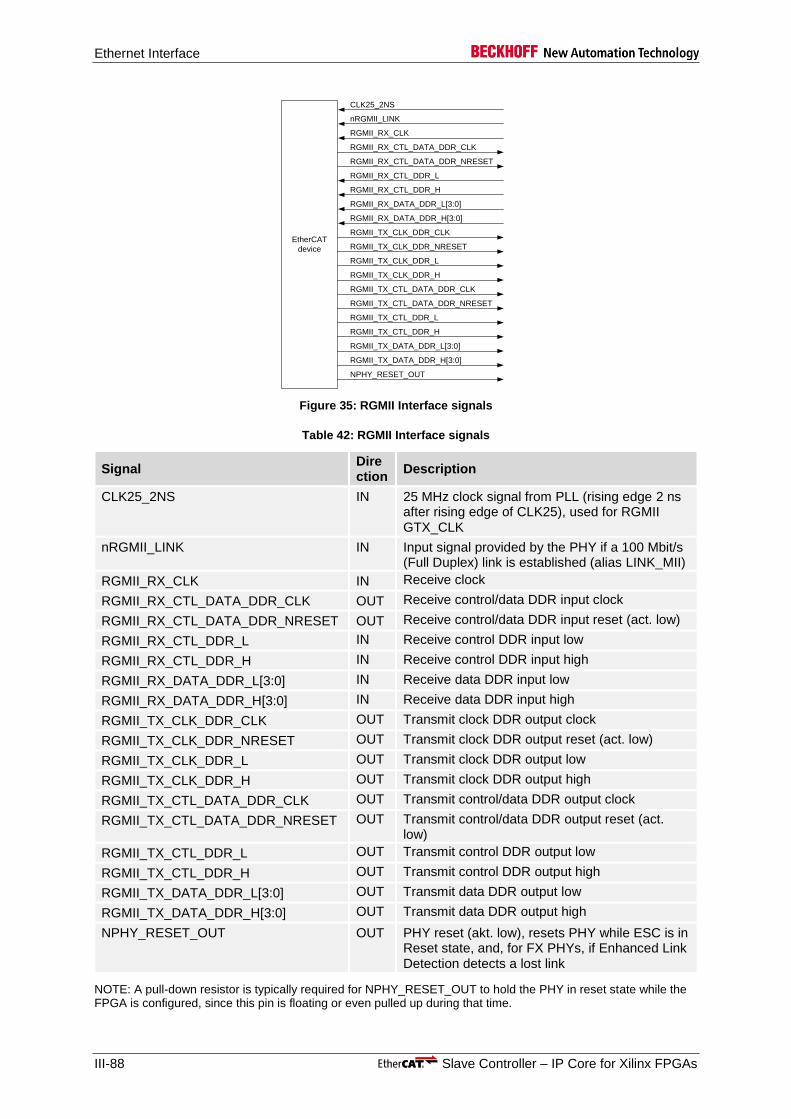
Ethernet Interface
III-88 Slave Controller – IP Core for Xilinx FPGAs
EtherCAT
device
nRGMII_LINK
CLK25_2NS
RGMII_RX_CLK
RGMII_RX_CTL_DATA_DDR_NRESET
RGMII_RX_CTL_DATA_DDR_CLK
RGMII_RX_CTL_DDR_L
RGMII_RX_CTL_DDR_H
NPHY_RESET_OUT
RGMII_RX_DATA_DDR_L[3:0]
RGMII_RX_DATA_DDR_H[3:0]
RGMII_TX_CLK_DDR_NRESET
RGMII_TX_CLK_DDR_CLK
RGMII_TX_CLK_DDR_L
RGMII_TX_CLK_DDR_H
RGMII_TX_CTL_DATA_DDR_NRESET
RGMII_TX_CTL_DATA_DDR_CLK
RGMII_TX_CTL_DDR_L
RGMII_TX_CTL_DDR_H
RGMII_TX_DATA_DDR_L[3:0]
RGMII_TX_DATA_DDR_H[3:0]
Figure 35: RGMII Interface signals
Table 42: RGMII Interface signals
Signal Direction
Description
CLK25_2NS IN 25 MHz clock signal from PLL (rising edge 2 ns after rising edge of CLK25), used for RGMII GTX_CLK
nRGMII_LINK IN Input signal provided by the PHY if a 100 Mbit/s (Full Duplex) link is established (alias LINK_MII)
RGMII_RX_CLK IN Receive clock
RGMII_RX_CTL_DATA_DDR_CLK OUT Receive control/data DDR input clock
RGMII_RX_CTL_DATA_DDR_NRESET OUT Receive control/data DDR input reset (act. low)
RGMII_RX_CTL_DDR_L IN Receive control DDR input low
RGMII_RX_CTL_DDR_H IN Receive control DDR input high
RGMII_RX_DATA_DDR_L[3:0] IN Receive data DDR input low
RGMII_RX_DATA_DDR_H[3:0] IN Receive data DDR input high
RGMII_TX_CLK_DDR_CLK OUT Transmit clock DDR output clock
RGMII_TX_CLK_DDR_NRESET OUT Transmit clock DDR output reset (act. low)
RGMII_TX_CLK_DDR_L OUT Transmit clock DDR output low
RGMII_TX_CLK_DDR_H OUT Transmit clock DDR output high
RGMII_TX_CTL_DATA_DDR_CLK OUT Transmit control/data DDR output clock
RGMII_TX_CTL_DATA_DDR_NRESET OUT Transmit control/data DDR output reset (act. low)
RGMII_TX_CTL_DDR_L OUT Transmit control DDR output low
RGMII_TX_CTL_DDR_H OUT Transmit control DDR output high
RGMII_TX_DATA_DDR_L[3:0] OUT Transmit data DDR output low
RGMII_TX_DATA_DDR_H[3:0] OUT Transmit data DDR output high
NPHY_RESET_OUT OUT PHY reset (akt. low), resets PHY while ESC is in Reset state, and, for FX PHYs, if Enhanced Link Detection detects a lost link
NOTE: A pull-down resistor is typically required for NPHY_RESET_OUT to hold the PHY in reset state while the FPGA is configured, since this pin is floating or even pulled up during that time.

Ethernet Interface
Slave Controller – IP Core for Xilinx FPGAs III-89
9.4.2 RGMII example schematic
Refer to chapter 8.5.3 for more information on special markings (!). Take care of proper PHY address configuration.
EtherCAT IP CoreEthernet PHY
RGMII_RX_CTL_DATA_DDR_CLK
RGMII_RX_CTL_DATA_DDR_NRESET
RGMII_RX_CLK
RX_CTL
RXD[3:0]
TX_CLK
RX_CLK
REF_CLK
TXD[3:0]
TX_CTL
nMII_LINK LINK_STATUS!
CLK25
PLL
CLK_IN CLK25
CLK100 CLK100
25 MHz
NPHY_RESET_OUT NRESET
4K
7
REF_CLK
CLK25_2NS CLK25_2NS DDR
input cellRGMII_RX_CTL_DDR_H
RGMII_RX_CTL_DDR_L
RGMII_RX_DATA_DDR_H[3:0]
RGMII_RX_DATA_DDR_L[3:0]
DDR
input cell
DDR
output
cell
DDR
output
cell
DDR
output
cell
RGMII_TX_CLK_DDR_CLK
RGMII_TX_CLK_DDR_NRESET
RGMII_TX_CLK_DDR_H
RGMII_TX_CLK_DDR_L
RGMII_TX_CTL_DATA_DDR_CLK
RGMII_TX_CTL_DATA_DDR_NRESET
RGMII_TX_CTL_DDR_H
RGMII_TX_CTL_DDR_L
RGMII_RX_DATA_DDR_H[3:0]
RGMII_RX_DATA_DDR_L[3:0]
Figure 36: RGMII example schematic
9.4.3 RGMII RX timing options
RGMII uses a source synchronous interface for receive signals. Originally, RX_CLK and RX_CTL/RX_DATA are edge-aligned at the PHY side. RX_CLK needs to be delayed to maintain setup/hold timing at the FPGA side. There are several options for delaying RX_CLK:
9.4.3.1 RX_CLK Delay in PHY
Some PHYs offer RGMII-ID, which means, the RX_CLK is delayed internally in the PHY. The EtherCAT IP Core itself cannot enable this feature using the MII management interface if the PHY requires this. It is up to the IP Core user to enable this feature.
9.4.3.2 RX_CLK Delay on PCB
One option is to delay RX_CLK on the PCB.
9.4.3.3 RX_CLK Delay in FPGA with PLL
The delay of RX_CLK can be realized with a PLL at each RGMII port, configured for clock phase shift.
9.4.3.4 RX_CLK Delay in FPGA without PLL
The delay of RX_CLK can be realized with routing delay inside the FPGA.
9.4.4 RGMII TX timing options
RGMII uses a source synchronous interface for receive signals. Originally, TX_CLK and TX_CTL/RX_DATA are edge-aligned at the FPGA side. TX_CLK needs to be delayed to maintain setup/hold timing at the PHY side. There are several options for delaying TX_CLK:

Ethernet Interface
III-90 Slave Controller – IP Core for Xilinx FPGAs
9.4.4.1 TX_CLK Delay in PHY
Some PHYs offer RGMII-ID, which means, the TX_CLK is delayed internally in the PHY. The EtherCAT IP Core itself cannot enable this feature using the MII management interface if the PHY requires this. It is up to the IP Core user to enable this feature.
9.4.4.2 TX_CLK Delay on PCB
One option is to delay TX_CLK on the PCB.
9.4.4.3 TX_CLK Delay in FPGA with PLL
The delay of TX_CLK can be realized with a PLL providing a delayed CLK25 attached to the CLK25_2NS input of the IP Core. This clock is used for the TX_CLK DDR output cell, while CLK25 is used for the TX_CTL/TX_DATA DDR output cells.
9.4.4.4 TX_CLK Delay in FPGA without PLL
The delay of TX_CLK can be realized with routing delay inside the FPGA.
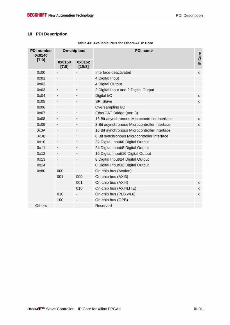
PDI Description
Slave Controller – IP Core for Xilinx FPGAs III-91
10 PDI Description
Table 43: Available PDIs for EtherCAT IP Core
PDI number
0x0140 [7:0]
On-chip bus PDI name
IP C
ore
0x0150 [7:5]
0x0152 [10:8]
0x00 - - Interface deactivated x
0x01 - - 4 Digital Input
0x02 - - 4 Digital Output
0x03 - - 2 Digital Input and 2 Digital Output
0x04 - - Digital I/O x
0x05 - - SPI Slave x
0x06 - - Oversampling I/O
0x07 - - EtherCAT Bridge (port 3)
0x08 - - 16 Bit asynchronous Microcontroller interface x
0x09 - - 8 Bit asynchronous Microcontroller interface x
0x0A - - 16 Bit synchronous Microcontroller interface
0x0B - - 8 Bit synchronous Microcontroller interface
0x10 - - 32 Digital Input/0 Digital Output
0x11 - - 24 Digital Input/8 Digital Output
0x12 - - 16 Digital Input/16 Digital Output
0x13 - - 8 Digital Input/24 Digital Output
0x14 - - 0 Digital Input/32 Digital Output
0x80 000 - On-chip bus (Avalon)
001 000 On-chip bus (AXI3)
001 On-chip bus (AXI4) x
010 On-chip bus (AXI4LITE) x
010 - On-chip bus (PLB v4.6) x
100 - On-chip bus (OPB)
Others Reserved

PDI Description
III-92 Slave Controller – IP Core for Xilinx FPGAs
10.1 Digital I/O Interface
10.1.1 Interface
The Digital I/O PDI is selected with PDI type 0x04. The signals of the Digital I/O interface are4:
EtherCAT
IP core
DATA_OUT[31:0]
LATCH_IN
OUTVALID
SOF
OE_EXT
WD_TRIG
DATA_IN[31:0] I/O[31:0]
DATA_ENA
Figure 37: IP core digital I/O signals
Table 44: IP core digital I/O signals
Signal Direction Description Signal polarity
DATA_OUT[31:0] OUT Output data
DATA_IN[31:0] IN Input data
LATCH_IN IN External data latch signal act. high
OUTVALID OUT Output data is valid/Output event act. high
SOF OUT Start of Frame act. high
OE_EXT IN Output Enable act. high
WD_TRIG OUT Watchdog Trigger act. high
DATA_ENA OUT Enable external Output data driver act. high
NOTE: Unsupported Digital I/O control signal OE_CONF is assumed to be low.
The Digital I/O PDI supports 1-4 byte of digital I/O signals, with each byte individually configurable as either input or output. At the IP core interface, the I/O signals are separated in input signals (DATA_IN) and output signals (DATA_OUT). The corresponding I/O bytes and addresses are listed below.
Table 45: Input/Output byte reference
I/O Byte
I/O signal Output signal Output address
Input signal Input address
0 I/O[7:0] DATA_OUT[7:0] 0x0F00 DATA_IN[7:0] 0x1000
1 I/O[15:8] DATA_OUT[15:8] 0x0F01 DATA_IN[15:8] 0x1001
2 I/O[23:16] DATA_OUT[23:16] 0x0F02 DATA_IN[23:16] 0x1002
3 I/O[31:24] DATA_OUT[31:24] 0x0F03 DATA_IN[31:24] 0x1003
4 The prefix `PDI_DIGI_` is added to the Digital I/O interface signals if the EtherCAT IP Core is used.
PDI Description
Slave Controller – IP Core for Xilinx FPGAs III-93
10.1.2 Configuration
The Digital I/O interface is selected with PDI type 0x04 in the PDI control register 0x0140. It supports different configurations, which are located in registers 0x0150 – 0x0153.
10.1.3 Digital Inputs
Digital input values appear in the process memory at address 0x1000:0x1003. EtherCAT devices use Little Endian byte ordering, so I/O[7:0] can be read at 0x1000 etc. Digital inputs are written to the process memory by the Digital I/O PDI using standard PDI write operations.
Digital inputs can be configured to be sampled by the ESC in four ways:
Digital inputs are sampled at the start of each Ethernet frame, so that EtherCAT read commands to address 0x1000:0x1003 will present digital input values sampled at the start of the same frame. The SOF signal can be used externally to update the input data, because the SOF is signaled before input data is sampled.
The sample time can be controlled externally by using the LATCH_IN signal. The input data is sampled by the ESC each time a rising edge of LATCH_IN is recognized.
Digital inputs are sampled at Distributed Clocks SYNC0 events.
Digital inputs are sampled at Distributed Clocks SYNC1 events.
For Distributed Clock SYNC input, SYNC generation must be activated (register 0x0981). SYNC output is not necessary (register 0x0151). SYNC pulse length (registers 0x0982:0x0983) should not be set to 0, because acknowledging of SYNC events is not possible with Digital I/O PDI. Sample time is the beginning of the SYNC event.
10.1.4 Digital Outputs
Digital Output values have to be written to register 0x0F00:0x0F03 (register 0x0F00 controls I/O[7:0] etc.). Digital Output values are not read by the Digital I/O PDI using standard read commands, instead, there is a direct connection for faster response times.
The process data watchdog (register 0x0440) has to be either active or disabled; otherwise digital outputs will not be updated. Digital outputs can be configured to be updated in four ways:
Digital Outputs are updated at the end of each EtherCAT frame (EOF mode).
Digital outputs are updated with Distributed Clocks SYNC0 events (DC SYNC0 mode).
Digital outputs are updated with Distributed Clocks SYNC1 events (DC SYNC1 mode).
Digital Outputs are updated at the end of an EtherCAT frame which triggered the Process Data Watchdog (with typical SyncManager configuration: a frame containing a write access to at least one of the registers 0x0F00:0x0F03). Digital Outputs are only updated if the EtherCAT frame was correct (WD_TRIG mode).
For Distributed Clock SYNC output, SYNC generation must be activated (register 0x0981). SYNC output is not necessary (register 0x0151). SYNC pulse length (registers 0x0982:0x0983) should not be set to 0, because acknowledging of SYNC events is not possible with Digital I/O PDI. Output time is the beginning of the SYNC event.
An output event is always signaled by a pulse on OUTVALID even if the digital outputs remain unchanged.
For output data to be visible on the I/O signals, the following conditions have to be met:
SyncManager watchdog must be either active (triggered) or disabled.
OE_EXT (Output enable) must be high.
Output values have to be written to the registers 0x0F00:0x0F03 within a valid EtherCAT frame.
The configured output update event must have occurred.
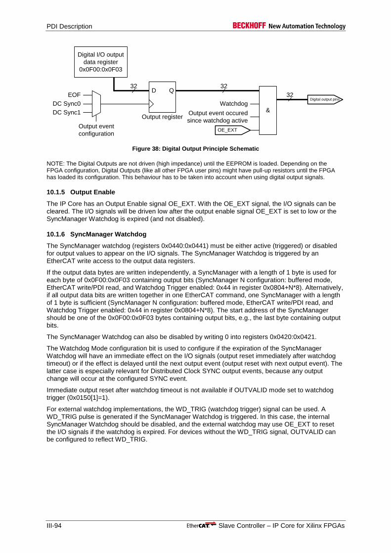
PDI Description
III-94 Slave Controller – IP Core for Xilinx FPGAs
32
Output register
Digital I/O output
data register
0x0F00:0x0F03
Watchdog&
32
32EOF
DC Sync0
DC Sync1
Digital output pins
OE_EXT
D Q
Output event
configuration
Output event occured
since watchdog active
Figure 38: Digital Output Principle Schematic
NOTE: The Digital Outputs are not driven (high impedance) until the EEPROM is loaded. Depending on the FPGA configuration, Digital Outputs (like all other FPGA user pins) might have pull-up resistors until the FPGA has loaded its configuration. This behaviour has to be taken into account when using digital output signals.
10.1.5 Output Enable
The IP Core has an Output Enable signal OE_EXT. With the OE_EXT signal, the I/O signals can be cleared. The I/O signals will be driven low after the output enable signal OE_EXT is set to low or the SyncManager Watchdog is expired (and not disabled).
10.1.6 SyncManager Watchdog
The SyncManager watchdog (registers 0x0440:0x0441) must be either active (triggered) or disabled for output values to appear on the I/O signals. The SyncManager Watchdog is triggered by an EtherCAT write access to the output data registers.
If the output data bytes are written independently, a SyncManager with a length of 1 byte is used for each byte of 0x0F00:0x0F03 containing output bits (SyncManager N configuration: buffered mode, EtherCAT write/PDI read, and Watchdog Trigger enabled: 0x44 in register 0x0804+N*8). Alternatively, if all output data bits are written together in one EtherCAT command, one SyncManager with a length of 1 byte is sufficient (SyncManager N configuration: buffered mode, EtherCAT write/PDI read, and Watchdog Trigger enabled: 0x44 in register 0x0804+N*8). The start address of the SyncManager should be one of the 0x0F00:0x0F03 bytes containing output bits, e.g., the last byte containing output bits.
The SyncManager Watchdog can also be disabled by writing 0 into registers 0x0420:0x0421.
The Watchdog Mode configuration bit is used to configure if the expiration of the SyncManager Watchdog will have an immediate effect on the I/O signals (output reset immediately after watchdog timeout) or if the effect is delayed until the next output event (output reset with next output event). The latter case is especially relevant for Distributed Clock SYNC output events, because any output change will occur at the configured SYNC event.
Immediate output reset after watchdog timeout is not available if OUTVALID mode set to watchdog trigger (0x0150[1]=1).
For external watchdog implementations, the WD_TRIG (watchdog trigger) signal can be used. A WD_TRIG pulse is generated if the SyncManager Watchdog is triggered. In this case, the internal SyncManager Watchdog should be disabled, and the external watchdog may use OE_EXT to reset the I/O signals if the watchdog is expired. For devices without the WD_TRIG signal, OUTVALID can be configured to reflect WD_TRIG.
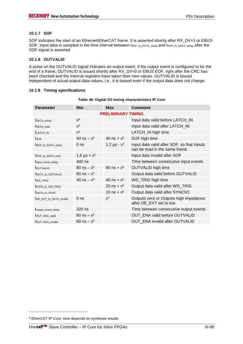
PDI Description
Slave Controller – IP Core for Xilinx FPGAs III-95
10.1.7 SOF
SOF indicates the start of an Ethernet/EtherCAT frame. It is asserted shortly after RX_DV=1 or EBUS SOF. Input data is sampled in the time interval between tSOF_to_DATA_setup and tSOF_to_DATA_setup after the SOF signal is asserted.
10.1.8 OUTVALID
A pulse on the OUTVALID signal indicates an output event. If the output event is configured to be the end of a frame, OUTVALID is issued shortly after RX_DV=0 or EBUS EOF, right after the CRC has been checked and the internal registers have taken their new values. OUTVALID is issued independent of actual output data values, i.e., it is issued even if the output data does not change.
10.1.9 Timing specifications
Table 46: Digital I/O timing characteristics IP Core
Parameter Min Max Comment
PRELIMINARY TIMING
tDATA_setup x5 Input data valid before LATCH_IN
tDATA_hold x5 Input data valid after LATCH_IN
tLATCH_IN x5 LATCH_IN high time
tSOF 40 ns – x5 40 ns + x5 SOF high time
tSOF_to_DATA_setup 0 ns 1,2 µs - x5 Input data valid after SOF, so that Inputs can be read in the same frame
tSOF_to_DATA_hold 1,6 µs + x5 Input data invalid after SOF
tinput_event_delay 440 ns Time between consecutive input events
tOUTVALID 80 ns – x5 80 ns + x5 OUTVALID high time
tDATA_to_OUTVALID 80 ns – x5 Output data valid before OUTVALID
tWD_TRIG 40 ns – x5 40 ns + x5 WD_TRIG high time
tDATA_to_WD_TRIG 20 ns + x5 Output data valid after WD_TRIG
tDATA_to_SYNC 10 ns + x5 Output data valid after SYNC0/1
tOE_EXT_to_DATA_invalid 0 ns x5 Outputs zero or Outputs high impedance after OE_EXT set to low
toutput_event_delay 320 ns Time between consecutive output events
tOUT_ENA_valid 80 ns – x5 OUT_ENA valid before OUTVALID
tOUT_ENA_invalid 80 ns – x5 OUT_ENA invalid after OUTVALID
5 EtherCAT IP Core: time depends on synthesis results
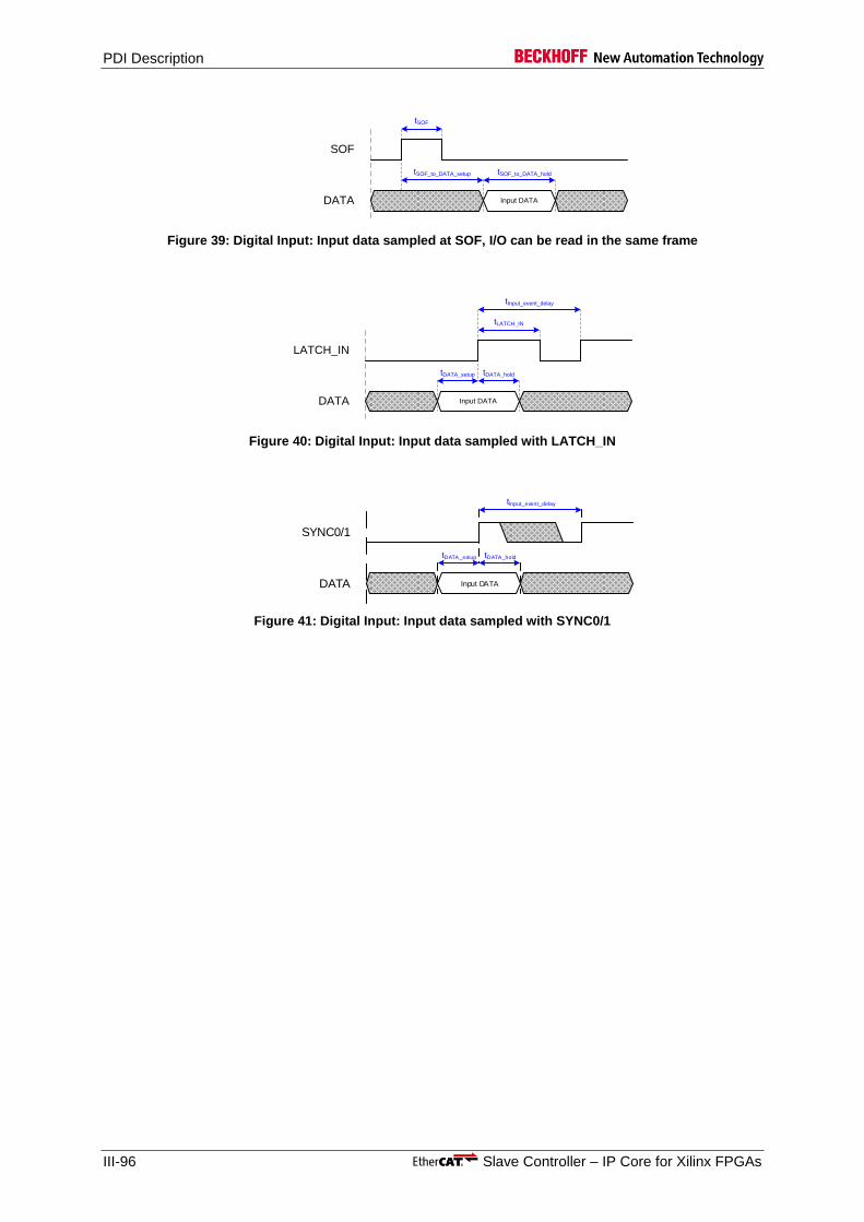
PDI Description
III-96 Slave Controller – IP Core for Xilinx FPGAs
SOF
DATA Input DATA
tSOF_to_DATA_setup
tSOF
tSOF_to_DATA_hold
Figure 39: Digital Input: Input data sampled at SOF, I/O can be read in the same frame
LATCH_IN
DATA Input DATA
tDATA_holdtDATA_setup
tLATCH_IN
tInput_event_delay
Figure 40: Digital Input: Input data sampled with LATCH_IN
SYNC0/1
DATA Input DATA
tDATA_holdtDATA_setup
tInput_event_delay
Figure 41: Digital Input: Input data sampled with SYNC0/1

PDI Description
Slave Controller – IP Core for Xilinx FPGAs III-97
OUTVALID
DATA
tDATA_to_OUTVALID
Output DATA
tOUTVALID
tOE_EXT_to_DATA_invalid
OE_EXT
WD_TRIG
tWD_TRIG
tDATA_to_WD_TRIG
toutput_event_delay
tDATA_to_SYNC
SYNC0/1
Zero or High-Impedance
Figure 42: Digital Output timing
OUTVALID
tOUT_ENA_valid tOUT_ENA_invalid
tOUTVALID
OUT_ENA
Figure 43: OUT_ENA timing
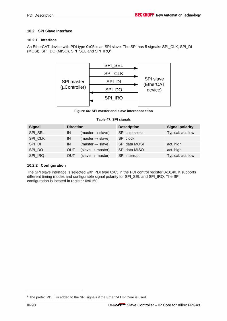
PDI Description
III-98 Slave Controller – IP Core for Xilinx FPGAs
10.2 SPI Slave Interface
10.2.1 Interface
An EtherCAT device with PDI type 0x05 is an SPI slave. The SPI has 5 signals: SPI_CLK, SPI_DI (MOSI), SPI_DO (MISO), SPI_SEL and SPI_IRQ6:
SPI master
(µController)
SPI_SEL
SPI_CLK
SPI_DI
SPI_DO
SPI_IRQ
SPI slave
(EtherCAT
device)
Figure 44: SPI master and slave interconnection
Table 47: SPI signals
Signal Direction Description Signal polarity
SPI_SEL IN (master → slave) SPI chip select Typical: act. low
SPI_CLK IN (master → slave) SPI clock
SPI_DI IN (master → slave) SPI data MOSI act. high
SPI_DO OUT (slave → master) SPI data MISO act. high
SPI_IRQ OUT (slave → master) SPI interrupt Typical: act. low
10.2.2 Configuration
The SPI slave interface is selected with PDI type 0x05 in the PDI control register 0x0140. It supports different timing modes and configurable signal polarity for SPI_SEL and SPI_IRQ. The SPI configuration is located in register 0x0150.
6 The prefix `PDI_` is added to the SPI signals if the EtherCAT IP Core is used.

PDI Description
Slave Controller – IP Core for Xilinx FPGAs III-99
10.2.3 SPI access
Each SPI access is separated into an address phase and a data phase. In the address phase, the SPI master transmits the first address to be accessed and the command. In the data phase, read data is presented by the SPI slave (read command) or write data is transmitted by the master (write command). The address phase consists of 2 or 3 bytes depending on the address mode. The number of data bytes for each access may range from 0 to N bytes. The slave internally increments the address for the following bytes after reading or writing the start address. The bits of both address/command and data are transmitted in byte groups.
The master starts an SPI access by asserting SPI_SEL and terminates it by taking back SPI_SEL (polarity determined by configuration). While SPI_SEL is asserted, the master has to cycle SPI_CLK eight times for each byte transfer. In each clock cycle, both master and slave transmit one bit to the other side (full duplex). The relevant edges of SPI_CLK for master and slave can be configured by selecting SPI mode and Data Out sample mode.
The most significant bit of a byte is transmitted first, the least significant bit last, the byte order is low byte first. EtherCAT devices use Little Endian byte ordering.
10.2.4 Address modes
The SPI slave interface supports two address modes, 2 byte addressing and 3 byte addressing. With two byte addressing, the lower 13 address bits A[12:0] are selected by the SPI master, while the upper 3 bits A[15:13] are assumed to be 000b inside the SPI slave, thus only the first 8 Kbyte in the EtherCAT slave address space can be accessed. Three byte addressing is used for accessing the whole 64 Kbyte address space of an EtherCAT slave.
For SPI masters which do only support consecutive transfers of more than one byte, additional Address Extension commands can be inserted.
Table 48: Address modes
Byte 2 Byte address mode 3 Byte address mode
0 A[12:5] address bits [12:5] A[12:5] address bits [12:5]
1 A[4:0] address bits [4:0]
CMD0[2:0] read/write command
A[4:0] address bits [4:0]
CMD0[2:0] 3 byte addressing: 110b
2 D0[7:0] data byte 0 A[15:13] address bits [15:13]
CMD1[2:0] read/write command
res[1:0] two reserved bits, set to 00b
3 D1[7:0] data byte 1 D0[7:0] data byte 0
4 ff. D2[7:0] data byte 2 D1[7:0] data byte 1

PDI Description
III-100 Slave Controller – IP Core for Xilinx FPGAs
10.2.5 Commands
The command CMD0 in the second address/command byte may be READ, READ with following Wait State bytes, WRITE, NOP, or Address Extension. The command CMD1 in the third address/command byte may have the same values:
Table 49: SPI commands CMD0 and CMD1
CMD[2] CMD[1] CMD[0] Command
0 0 0 NOP (no operation)
0 0 1 reserved
0 1 0 Read
0 1 1 Read with following Wait State bytes
1 0 0 Write
1 0 1 reserved
1 1 0 Address Extension (3 address/command bytes)
1 1 1 reserved
10.2.6 Interrupt request register (AL Event register)
During the address phase, the SPI slave transmits the PDI interrupt request registers 0x0220-0x0221 (2 byte address mode), and additionally register 0x0222 for 3 byte addressing on SPI_DO (MISO):
Table 50: Interrupt request register transmission
Byte
2 Byte address mode 3 Byte address mode
SPI_DI (MOSI)
SPI_DO (MISO)
SPI_DI (MOSI)
SPI_DO (MISO)
0 A[12:5] I0[7:0] interrupt request register 0x0220
A[12:5] I0[7:0] interrupt request register 0x0220
1 A[4:0]
CMD0[2:0]
I1[7:0] interrupt request register 0x0221
A[4:0] CMD0[2:0]
I1[7:0] interrupt request register 0x0221
2 (Data phase) A[15:13] CMD1[2:0]
I2[7:0] interrupt request register 0x0222
10.2.7 Write access
In the data phase of a write access, the SPI master sends the write data bytes to the SPI slave (SPI_DI/MOSI). The write access is terminated by taking back SPI_SEL after the last byte. The SPI_DO signal (MISO) is undetermined during the data phase of write accesses.
10.2.8 Read access
In the data phase of a read access, the SPI slave sends the read data bytes to the SPI master (SPI_DO/MISO).
PDI Description
Slave Controller – IP Core for Xilinx FPGAs III-101
10.2.8.1 Read Wait State
Between the last address phase byte and the first data byte of a read access, the SPI master has to wait for the SPI slave to fetch the read data internally. Subsequent read data bytes are prefetched automatically, so no further wait states are necessary.
The SPI master can choose between these possibilities:
The SPI master may either wait for the specified worst case internal read time tread after the last address/command byte and before the first clock cycle of the data phase.
The SPI master inserts one Wait State byte after the last address/command byte. The Wait State byte must have a value of 0xFF transferred on SPI_DI.
10.2.8.2 Read Termination
The SPI_DI signal (MOSI) is used for termination of the read access by the SPI master. For the last data byte, the SPI master has to set SPI_DI to high (Read Termination byte = 0xFF), so the slave will not prefetch the next read data internally. If SPI_DI is low during a data byte transfer, at least one more byte will be read by the master afterwards.
10.2.9 SPI access errors and SPI status flag
The following reasons for SPI access errors are detected by the SPI slave:
The number of clock cycles recognized while SPI_SEL is asserted is not a multiple of 8 (incomplete bytes were transferred).
For a read access, a clock cycle occurred while the slave was busy fetching the first data byte.
For a read access, the data phase was not terminated by setting SPI_DI to high for the last byte.
For a read access, additional bytes were read after termination of the access.
A wrong SPI access will have these consequences:
Registers will not accept write data (nevertheless, RAM will be written).
Special functions are not executed (e.g., SyncManager buffer switching).
The PDI error counter 0x030D will be incremented.
A status flag will indicate the error until the next access (not for SPI mode 0/2 with normal data out sample)
A status flag, which indicates if the last access had an error, is available in any mode except for SPI mode 0/2 with normal data out sample. The status flag is presented on SPI_DO (MISO) after the slave is selected (SPI_SEL) and until the first clock cycle occurs. So the status can be read either between two accesses by assertion of SPI_SEL without clocking, or at the beginning of an access just before the first clock cycle. The status flag will be high for a good access, and low for a wrong access.
The reason of the access error can be read in the PDI error code register 0x030E.
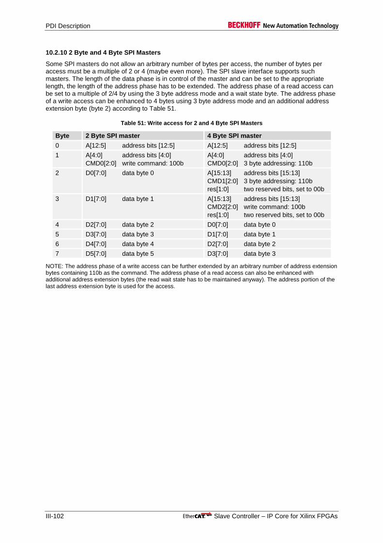
PDI Description
III-102 Slave Controller – IP Core for Xilinx FPGAs
10.2.10 2 Byte and 4 Byte SPI Masters
Some SPI masters do not allow an arbitrary number of bytes per access, the number of bytes per access must be a multiple of 2 or 4 (maybe even more). The SPI slave interface supports such masters. The length of the data phase is in control of the master and can be set to the appropriate length, the length of the address phase has to be extended. The address phase of a read access can be set to a multiple of 2/4 by using the 3 byte address mode and a wait state byte. The address phase of a write access can be enhanced to 4 bytes using 3 byte address mode and an additional address extension byte (byte 2) according to Table 51.
Table 51: Write access for 2 and 4 Byte SPI Masters
Byte 2 Byte SPI master 4 Byte SPI master
0 A[12:5] address bits [12:5] A[12:5] address bits [12:5]
1 A[4:0] address bits [4:0]
CMD0[2:0] write command: 100b
A[4:0] address bits [4:0]
CMD0[2:0] 3 byte addressing: 110b
2 D0[7:0] data byte 0 A[15:13] address bits [15:13]
CMD1[2:0] 3 byte addressing: 110b
res[1:0] two reserved bits, set to 00b
3 D1[7:0] data byte 1 A[15:13] address bits [15:13]
CMD2[2:0] write command: 100b
res[1:0] two reserved bits, set to 00b
4 D2[7:0] data byte 2 D0[7:0] data byte 0
5 D3[7:0] data byte 3 D1[7:0] data byte 1
6 D4[7:0] data byte 4 D2[7:0] data byte 2
7 D5[7:0] data byte 5 D3[7:0] data byte 3
NOTE: The address phase of a write access can be further extended by an arbitrary number of address extension bytes containing 110b as the command. The address phase of a read access can also be enhanced with additional address extension bytes (the read wait state has to be maintained anyway). The address portion of the last address extension byte is used for the access.
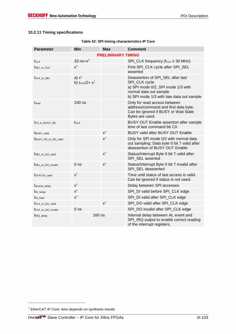
PDI Description
Slave Controller – IP Core for Xilinx FPGAs III-103
10.2.11 Timing specifications
Table 52: SPI timing characteristics IP Core
Parameter Min Max Comment
PRELIMINARY TIMING
tCLK 33 ns+x7 SPI_CLK frequency (fCLK ≤ 30 MHz)
tSEL_to_CLK x7 First SPI_CLK cycle after SPI_SEL asserted
tCLK_to_SEL a) x7
b) tCLK/2+ x7
Deassertion of SPI_SEL after last SPI_CLK cycle
a) SPI mode 0/2, SPI mode 1/3 with normal data out sample
b) SPI mode 1/3 with late data out sample
tread 240 ns Only for read access between address/command and first data byte. Can be ignored if BUSY or Wait State Bytes are used.
tC0_to_BUSY_OE tCLK BUSY OUT Enable assertion after sample time of last command bit C0.
tBUSY_valid x7 BUSY valid after BUSY OUT Enable
tBUSY_OE_to_DO_valid x7 Only for SPI mode 0/2 with normal data out sampling: Data byte 0 bit 7 valid after deassertion of BUSY OUT Enable
tSEL_to_DO_valid x7 Status/Interrupt Byte 0 bit 7 valid after SPI_SEL asserted
tSEL_to_DO_invalid 0 ns x7 Status/Interrupt Byte 0 bit 7 invalid after SPI_SEL deasserted
tSTATUS_valid x7 Time until status of last access is valid. Can be ignored if status is not used.
taccess_delay x7 Delay between SPI accesses
tDI_setup x7 SPI_DI valid before SPI_CLK edge
tDI_hold x7 SPI_DI valid after SPI_CLK edge
tCLK_to_DO_valid x7 SPI_DO valid after SPI_CLK edge
tCLK_to_DO_invalid 0 ns SPI_DO invalid after SPI_CLK edge
tIRQ_delay 160 ns Internal delay between AL event and SPI_IRQ output to enable correct reading of the interrupt registers.
7 EtherCAT IP Core: time depends on synthesis results
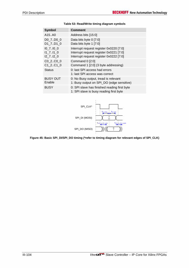
PDI Description
III-104 Slave Controller – IP Core for Xilinx FPGAs
Table 53: Read/Write timing diagram symbols
Symbol Comment
A15..A0 Address bits [15:0]
D0_7..D0_0
D1_7..D1_0
Data bits byte 0 [7:0]
Data bits byte 1 [7:0]
I0_7..I0_0
I1_7..I1_0
I2_7..I2_0
Interrupt request register 0x0220 [7:0]
Interrupt request register 0x0221 [7:0]
Interrupt request register 0x0222 [7:0]
C0_2..C0_0
C1_2..C1_0
Command 0 [2:0]
Command 1 [2:0] (3 byte addressing)
Status 0: last SPI access had errors
1: last SPI access was correct
BUSY OUT Enable
0: No Busy output, tread is relevant
1: Busy output on SPI_DO (edge sensitive)
BUSY 0: SPI slave has finished reading first byte
1: SPI slave is busy reading first byte
SPI_DO (MISO)
SPI_DI (MOSI)
SPI_CLK*
tDI_setup tDI_hold
tCLK_to_DO_valid
A
12
tCLK_to_DO_invalid
I0
7
Figure 45: Basic SPI_DI/SPI_DO timing (*refer to timing diagram for relevant edges of SPI_CLK)

PDI Description
Slave Controller – IP Core for Xilinx FPGAs III-105
C0 0
SP
I_S
EL
SP
I_C
LK
mo
de
0
SP
I_C
LK
mo
de
2
SP
I_C
LK
mo
de
3
SP
I_C
LK
mo
de
1
SP
I_D
O (
MIS
O)
late
sa
mp
le, m
od
e 1
/3
SP
I_D
O (
MIS
O)
late
sa
mp
le, m
od
e 0
/2
SP
I_D
O (
MIS
O)
no
rma
l sa
mp
le, m
od
e 1
/3
SP
I_D
O (
MIS
O)
no
rma
l sa
mp
le, m
od
e 0
/2
A 12
A 11
A 10
A 9
A 8
A 7
A 6
A 5
A 4
A 3
A 2
A 1
A 0S
PI_
DI (M
OS
I)
I0 7
I0 6
I0 5
I0 4
I0 3
I0 2
I0 1
I0 0
I1 7
I1 6
I1 5
I1 4
I1 3
I1 2
I1 1S
tatu
s
I0 6
I0 5
I0 4
I0 3
I0 2
I0 1
I0 0
I1 7
I1 6
I1 5
I1 4
I1 3
I1 2
I1 1
I0 7
I0 6
I0 5
I0 4
I0 3
I0 2
I0 1
I0 0
I1 7
I1 6
I1 5
I1 4
I1 3
I1 2
I1 1
I0 7
Sta
tus
I0 6
I0 5
I0 4
I0 3
I0 2
I0 1
I1 7
I1 6
I1 5
I1 4
I1 3
I1 2
I1 1
A 12
A 11
A 10
A 9
A 8
A 7
A 6
A 5
A 4
A 3
A 2
A 1
A 0S
PI_
DI (M
OS
I)
D0 7
D0 6
D0 5
D0 4
D0 3
D0 2
D0 1
D0 6
D0 5
D0 4
D0 3
D0 2
D0 1
t SE
L_to
_C
LK
t CL
K
t CL
K
t SE
L_
to_
DO
_va
lid
t SE
L_
to_
CL
Kt C
LK
_to
_S
EL
t CL
K_to
_S
EL
Re
ad
Te
rmin
atio
n b
yte
D0 0
t SE
L_
to_
DO
_in
va
lid
SPI mode 1/3SPI mode 0/2
Ad
dre
ss/C
om
ma
nd
Byte
0A
dd
ress/C
om
ma
nd
Byte
1W
ait S
tate
byte
Da
ta B
yte
0
C0 2
C0 1
C0 2
C0 1
I1 0
D0 7
Wa
it S
tate
byte
D0 7
D0 6
D0 5
D0 4
D0 3
D0 2
D0 1
D0 6
D0 5
D0 4
D0 3
D0 2
D0 1
D0 0
D0 0
I1 0
I1 0
D0 7
C0 0
Re
ad
Te
rmin
atio
n b
yte
Wa
it S
tate
byte
I0 0
I1 0
D0 0
I0 7S
tatu
s
Fig
ure
46
: S
PI
read
acc
es
s (
2 b
yte
ad
dre
ss
ing
, 1
by
te r
ea
d d
ata
) w
ith
Wa
it S
tate
by
te
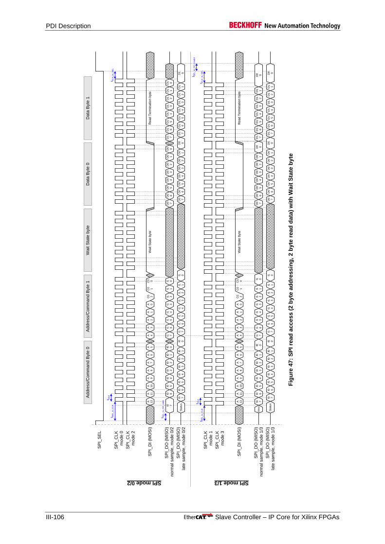
PDI Description
III-106 Slave Controller – IP Core for Xilinx FPGAs
C0 0
SP
I_S
EL
SP
I_C
LK
mo
de
0
SP
I_C
LK
mo
de
2
SP
I_C
LK
mo
de
3
SP
I_C
LK
mo
de
1
SP
I_D
O (
MIS
O)
late
sa
mp
le, m
od
e 1
/3
SP
I_D
O (
MIS
O)
late
sa
mp
le, m
od
e 0
/2
SP
I_D
O (
MIS
O)
no
rma
l sa
mp
le, m
od
e 1
/3
SP
I_D
O (
MIS
O)
no
rma
l sa
mp
le, m
od
e 0
/2
A 12
A 11
A 10
A 9
A 8
A 7
A 6
A 5
A 4
A 3
A 2
A 1
A 0S
PI_
DI (M
OS
I)
I0 7
I0 6
I0 5
I0 4
I0 3
I0 2
I0 1
I0 0
I1 7
I1 6
I1 5
I1 4
I1 3
I1 2
I1 1S
tatu
s
I0 6
I0 5
I0 4
I0 3
I0 2
I0 1
I0 0
I1 7
I1 6
I1 5
I1 4
I1 3
I1 2
I1 1
I0 7
I0 6
I0 5
I0 4
I0 3
I0 2
I0 1
I0 0
I1 7
I1 6
I1 5
I1 4
I1 3
I1 2
I1 1
I0 7
Sta
tus
I0 6
I0 5
I0 4
I0 3
I0 2
I0 1
I1 7
I1 6
I1 5
I1 4
I1 3
I1 2
I1 1
A 12
A 11
A 10
A 9
A 8
A 7
A 6
A 5
A 4
A 3
A 2
A 1
A 0S
PI_
DI (M
OS
I)
t SE
L_
to_
CL
K
t CL
K
t CL
K
t SE
L_
to_
DO
_va
lid
t SE
L_
to_
CL
Kt C
LK
_to
_S
EL
t CL
K_
to_
SE
L
Re
ad
Te
rmin
atio
n b
yte
D1 0
t SE
L_
to_
DO
_in
va
lid
SPI mode 1/3SPI mode 0/2
Ad
dre
ss/C
om
ma
nd
Byte
0A
dd
ress/C
om
ma
nd
Byte
1W
ait S
tate
byte
Da
ta B
yte
1
C0 2
C0 1
C0 2
C0 1
I1 0
Wa
it S
tate
byte
D0 0
D0 0
I1 0
I1 0
C0 0
Re
ad
Te
rmin
atio
n b
yte
Wa
it S
tate
byte
I0 0
I1 0
I0 7S
tatu
sD
0 7
D0 6
D0 5
D0 4
D0 3
D0 2
D0 1
D0 6
D0 5
D0 4
D0 3
D0 2
D0 1
D0 7
D0 6
D0 5
D0 4
D0 3
D0 2
D0 1
D0 6
D0 5
D0 4
D0 3
D0 2
D0 1
D0 0
D0 7
Da
ta B
yte
0
D0 7
D0 0
D0 0 D0 0
D1 7
D1 6
D1 5
D1 4
D1 3
D1 2
D1 1
D1 7
D1 6
D1 5
D1 4
D1 3
D1 2
D1 1
D1 7
D1 6
D1 5
D1 4
D1 3
D1 2
D1 1
D1 7
D1 6
D1 5
D1 4
D1 3
D1 2
D1 1
D1 0
Fig
ure
47
: S
PI
read
acc
es
s (
2 b
yte
ad
dre
ss
ing
, 2
by
te r
ea
d d
ata
) w
ith
Wa
it S
tate
by
te
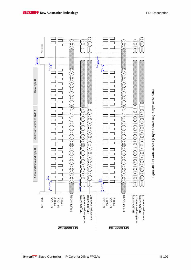
PDI Description
Slave Controller – IP Core for Xilinx FPGAs III-107
SP
I_S
EL
SP
I_C
LK
mo
de
0
SP
I_C
LK
mo
de
2
SP
I_C
LK
mo
de
3
SP
I_C
LK
mo
de
1
SP
I_D
O (
MIS
O)
late
sa
mp
le, m
od
e 1
/3
SP
I_D
O (
MIS
O)
late
sa
mp
le, m
od
e 0
/2
SP
I_D
O (
MIS
O)
no
rma
l sa
mp
le, m
od
e 1
/3
SP
I_D
O (
MIS
O)
no
rma
l sa
mp
le, m
od
e 0
/2
A 12
A 11
A 10
A 9
A 8
A 7
A 6
A 5
A 4
A 3
A 2
A 1
A 0S
PI_
DI (M
OS
I)
I0 7
I0 6
I0 5
I0 4
I0 3
I0 2
I0 1
I0 0
I1 7
I1 6
I1 5
I1 4
I1 3
I1 2
I1 1S
tatu
s
I0 6
I0 5
I0 4
I0 3
I0 2
I0 1
I0 0
I1 7
I1 6
I1 5
I1 4
I1 3
I1 2
I1 1
I0 7
I0 6
I0 5
I0 4
I0 3
I0 2
I0 1
I0 0
I1 7
I1 6
I1 5
I1 4
I1 3
I1 2
I1 1
I0 7
Sta
tus
I0 6
I0 5
I0 4
I0 3
I0 2
I0 1
I1 7
I1 6
I1 5
I1 4
I1 3
I1 2
I1 1
A 12
A 11
A 10
A 9
A 8
A 7
A 6
A 5
A 4
A 3
A 2
A 1
A 0S
PI_
DI (M
OS
I)
t SE
L_
to_
CL
K
t CL
K
t CL
K
t SE
L_
to_
DO
_va
lid
t SE
L_
to_
CL
K
SPI mode 1/3SPI mode 0/2
Ad
dre
ss/C
om
ma
nd
Byte
0A
dd
ress/C
om
ma
nd
Byte
1D
ata
Byte
0
D0 7
D0 6
D0 5
D0 4
D0 3
D0 2
D0 1
D0 0
I1 0
D0 7
D0 6
D0 5
D0 4
D0 3
D0 2
D0 1
D0 0
I1 0
I1 0
A 12
A 11
I0 7
I0 6I0 6
I0 7
I0 6
I0 7
Sta
tus
I0 6
A 12
A 11
Ne
xt a
cce
ss
t acce
ss_
de
lay
t CL
K_
to_
SE
L
t CL
K_
to_
SE
L
t SE
L_
to_
DO
_in
va
lid
C0 2
C0 1
C0 0
C0 2
C0 1
C0 0
I0 0
I1 0
I0 7S
tatu
sI0 7
Sta
tus
Sta
tus
Fig
ure
48
: S
PI
wri
te a
cc
es
s (
2 b
yte
ad
dre
ss
ing
, 1
by
te w
rite
da
ta)
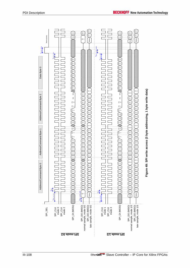
PDI Description
III-108 Slave Controller – IP Core for Xilinx FPGAs
SP
I_S
EL
SP
I_C
LK
mo
de
0
SP
I_C
LK
mo
de
2
SP
I_C
LK
mo
de
3
SP
I_C
LK
mo
de
1
SP
I_D
O (
MIS
O)
late
sa
mp
le, m
od
e 1
/3
SP
I_D
O (
MIS
O)
late
sa
mp
le, m
od
e 0
/2
SP
I_D
O (
MIS
O)
no
rma
l sa
mp
le, m
od
e 1
/3
SP
I_D
O (
MIS
O)
no
rma
l sa
mp
le, m
od
e 0
/2
A 12
A 11
A 10
A 9
A 8
A 7
A 6
A 5
A 4
A 3
A 2
A 1
A 0S
PI_
DI (M
OS
I)
I0 7
I0 6
I0 5
I0 4
I0 3
I0 2
I0 1
I0 0
I1 7
I1 6
I1 5
I1 4
I1 3
I1 2
I1 1S
tatu
s
I0 6
I0 5
I0 4
I0 3
I0 2
I0 1
I0 0
I1 7
I1 6
I1 5
I1 4
I1 3
I1 2
I1 1
I0 7
I0 6
I0 5
I0 4
I0 3
I0 2
I0 1
I0 0
I1 7
I1 6
I1 5
I1 4
I1 3
I1 2
I1 1
I0 7
Sta
tus
I0 6
I0 5
I0 4
I0 3
I0 2
I0 1
I1 7
I1 6
I1 5
I1 4
I1 3
I1 2
I1 1
A 12
A 11
A 10
A 9
A 8
A 7
A 6
A 5
A 4
A 3
A 2
A 1
A 0S
PI_
DI (M
OS
I)
t SE
L_
to_
CL
K
t CL
K
t CL
K
t SE
L_
to_
DO
_va
lid
t SE
L_
to_
CL
K
SPI mode 1/3SPI mode 0/2
Ad
dre
ss/C
om
ma
nd
Byte
0A
dd
ress/C
om
ma
nd
Byte
1D
ata
Byte
0
A 15
A 14
A 13
D0 7
D0 6
D0 5
D0 4
D0 3
D0 2
D0 1
D0 0
I2 7
I2 6
I2 5
I2 4
I2 3
I2 2
I2 1
I1 0
I2 7
I2 6
I2 5
I2 4
I2 3
I2 2
I2 1
A 15
A 14
A 13
D0 7
D0 6
D0 5
D0 4
D0 3
D0 2
D0 1
D0 0
Ad
dre
ss/C
om
ma
nd
Byte
2
I2 0
I1 0
I2 7
I2 6
I2 5
I2 4
I2 3
I2 2
I2 1
I1 0
I2 7
I2 6
I2 5
I2 4
I2 3
I2 2
I2 1
I2 0
I2 0
A 12
A 11
I0 7
I0 6I0 6
I0 7
I0 6
I0 7
Sta
tus
I0 6
A 12
A 11
Ne
xt a
cce
ss
t acce
ss_
de
lay
t CL
K_
to_
SE
L
t CL
K_
to_
SE
L
t SE
L_
to_
DO
_in
va
lid
C0 2
C0 1
C0 0
C1 2
C1 1
C1 0
res
res
C0 2
C0 1
C0 0
C1 2
C1 1
C1 0
res
res
I0 0
I1 0
I2 0
I0 7S
tatu
sI0 7
Sta
tus
Sta
tus
Fig
ure
49
: S
PI
wri
te a
cc
es
s (
3 b
yte
ad
dre
ss
ing
, 1
by
te w
rite
da
ta)
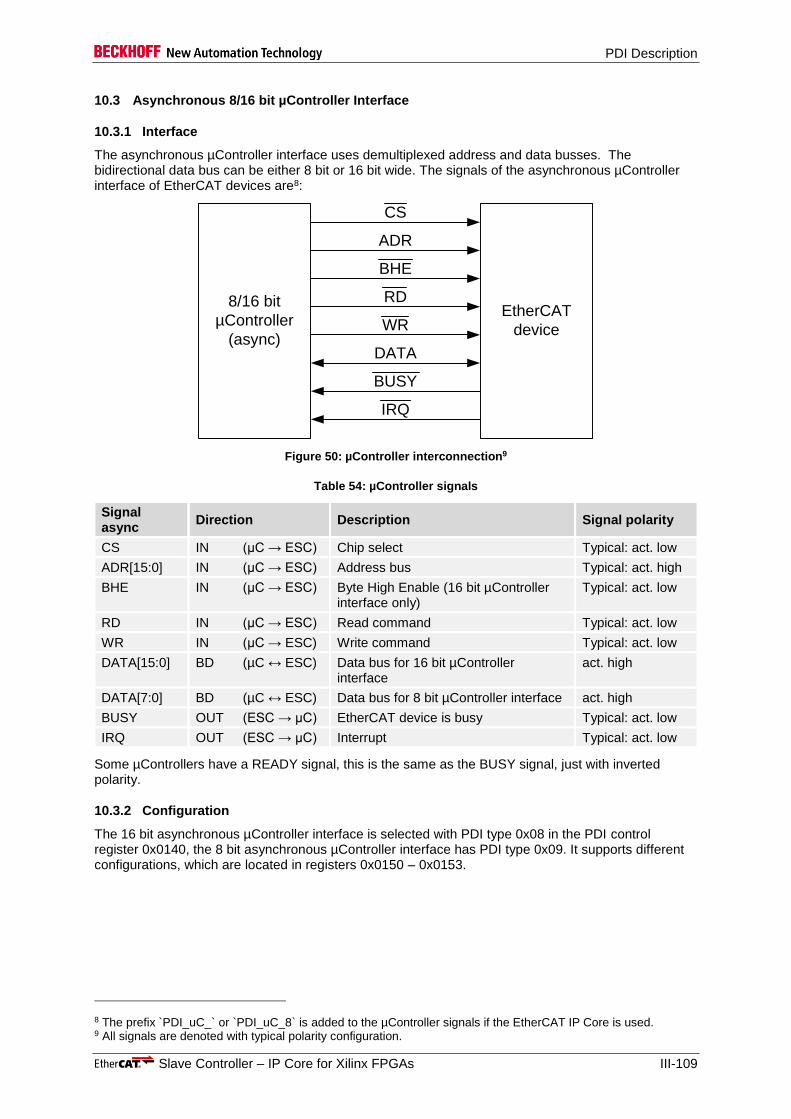
PDI Description
Slave Controller – IP Core for Xilinx FPGAs III-109
10.3 Asynchronous 8/16 bit µController Interface
10.3.1 Interface
The asynchronous µController interface uses demultiplexed address and data busses. The bidirectional data bus can be either 8 bit or 16 bit wide. The signals of the asynchronous µController interface of EtherCAT devices are8:
8/16 bit
µController
(async)
CS
ADR
BHE
DATA
BUSY
EtherCAT
device
IRQ
RD
WR
Figure 50: µController interconnection9
Table 54: µController signals
Signal async
Direction Description Signal polarity
CS IN (µC → ESC) Chip select Typical: act. low
ADR[15:0] IN (µC → ESC) Address bus Typical: act. high
BHE IN (µC → ESC) Byte High Enable (16 bit µController interface only)
Typical: act. low
RD IN (µC → ESC) Read command Typical: act. low
WR IN (µC → ESC) Write command Typical: act. low
DATA[15:0] BD (µC ↔ ESC) Data bus for 16 bit µController interface
act. high
DATA[7:0] BD (µC ↔ ESC) Data bus for 8 bit µController interface act. high
BUSY OUT (ESC → µC) EtherCAT device is busy Typical: act. low
IRQ OUT (ESC → µC) Interrupt Typical: act. low
Some µControllers have a READY signal, this is the same as the BUSY signal, just with inverted polarity.
10.3.2 Configuration
The 16 bit asynchronous µController interface is selected with PDI type 0x08 in the PDI control register 0x0140, the 8 bit asynchronous µController interface has PDI type 0x09. It supports different configurations, which are located in registers 0x0150 – 0x0153.
8 The prefix `PDI_uC_` or `PDI_uC_8` is added to the µController signals if the EtherCAT IP Core is used. 9 All signals are denoted with typical polarity configuration.

PDI Description
III-110 Slave Controller – IP Core for Xilinx FPGAs
10.3.3 µController access
The 8 bit µController interface reads or writes 8 bit per access, the 16 bit µController interface supports both 8 bit and 16 bit read/write accesses. For the 16 bit µController interface, the least significant address bit together with Byte High Enable (BHE) are used to distinguish between 8 bit low byte access, 8 bit high byte access and 16 bit access.
EtherCAT devices use Little Endian byte ordering.
Table 55: 8 bit µController interface access types
ADR[0] Access DATA[7:0]
0 8 bit access to ADR[15:0] (low byte, even address) low byte
1 8 bit access to ADR[15:0] (high byte, odd address) high byte
Table 56: 16 bit µController interface access types
ADR[0] BHE (act. low)
Access DATA [15:8]
DATA [7:0]
0 0 16 bit access to ADR[15:0] and ADR[15:0]+1 (low and high byte)
high byte low byte
0 1 8 bit access to ADR[15:0] (low byte, even address)
(RD only: copy of low byte)
low byte
1 0 8 bit access to ADR[15:0] (high byte, odd address)
high byte (RD only: copy of high byte)
1 1 invalid access - -
10.3.4 Write access
A write access starts with assertion of Chip Select (CS), if it is not permanently asserted. Address, Byte High Enable and Write Data are asserted with the falling edge of WR (active low). Once the µController interface is not BUSY, a rising edge on WR completes the µController access. A write access can be terminated either by deassertion of WR (while CS remains asserted), or by deassertion or CS (while WR remains asserted), or even by deassertion of WR and CS simultaneously. Shortly after the rising edge of WR, the access can be finished by deasserting ADR, BHE and DATA. The µController interface indicates its internal operation with the BUSY signal. Since the BUSY signal is only driven while CS is asserted, the BUSY driver will be released after CS deassertion.
Depending on the configuration, the internal write access is either performed after the falling edge of WR, or after the rising edge of WR. If the falling edge is selected, the internal write operation begins with the falling edge of WR, and BUSY indicates when the write operation is finished. The internal write operation is performed during the external write access.
If the rising edge of WR is selected, the internal operation begins with the rising edge of WR, i.e., after the external write access. Thus, the external write access is very fast, but an access immediately following will be delayed by the preceding write access. The maximum access time is higher in this case.
10.3.5 Read access
A read access starts with assertion of Chip Select (CS), if it is not permanently asserted. Address and BHE have to be valid before the falling edge of RD, which signals the start of the access. The µController interface will show its BUSY state afterwards – if it is not already busy executing a preceding write access – and release BUSY when the read data are valid. The read data will remain valid until either ADR, BHE, RD or CS change. The data bus will be driven while CS and RD are asserted. BUSY will be driven while CS is asserted.
With read busy delay configuration, BUSY deassertion for read accesses can be additionally delayed for 15 ns, so external DATA setup requirements in respect to BUSY can be met.
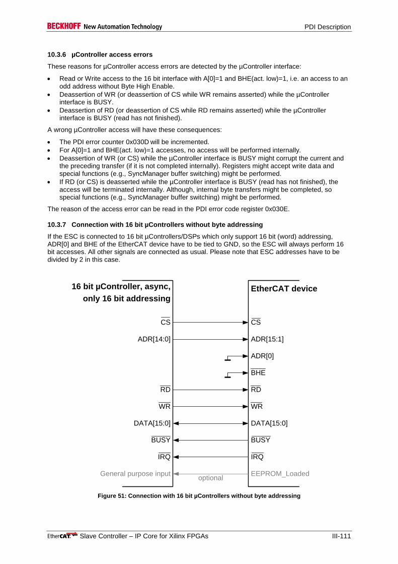
PDI Description
Slave Controller – IP Core for Xilinx FPGAs III-111
10.3.6 µController access errors
These reasons for µController access errors are detected by the µController interface:
Read or Write access to the 16 bit interface with A[0]=1 and BHE(act. low)=1, i.e. an access to an odd address without Byte High Enable.
Deassertion of WR (or deassertion of CS while WR remains asserted) while the µController interface is BUSY.
Deassertion of RD (or deassertion of CS while RD remains asserted) while the µController interface is BUSY (read has not finished).
A wrong µController access will have these consequences:
The PDI error counter 0x030D will be incremented.
For A[0]=1 and BHE(act. low)=1 accesses, no access will be performed internally.
Deassertion of WR (or CS) while the µController interface is BUSY might corrupt the current and the preceding transfer (if it is not completed internally). Registers might accept write data and special functions (e.g., SyncManager buffer switching) might be performed.
If RD (or CS) is deasserted while the µController interface is BUSY (read has not finished), the access will be terminated internally. Although, internal byte transfers might be completed, so special functions (e.g., SyncManager buffer switching) might be performed.
The reason of the access error can be read in the PDI error code register 0x030E.
10.3.7 Connection with 16 bit µControllers without byte addressing
If the ESC is connected to 16 bit µControllers/DSPs which only support 16 bit (word) addressing, ADR[0] and BHE of the EtherCAT device have to be tied to GND, so the ESC will always perform 16 bit accesses. All other signals are connected as usual. Please note that ESC addresses have to be divided by 2 in this case.
CS CS
ADR[14:0]
RD
BUSY
DATA[15:0]
WR
ADR[15:1]
ADR[0]
RD
BUSY
DATA[15:0]
WR
16 bit µController, async,
only 16 bit addressing
EtherCAT device
IRQ IRQ
BHE
General purpose input EEPROM_Loadedoptional
Figure 51: Connection with 16 bit µControllers without byte addressing
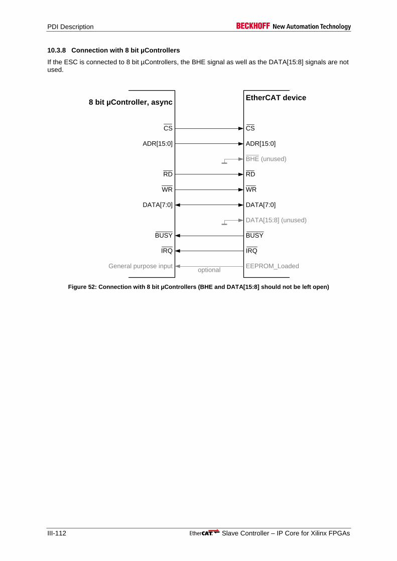
PDI Description
III-112 Slave Controller – IP Core for Xilinx FPGAs
10.3.8 Connection with 8 bit µControllers
If the ESC is connected to 8 bit µControllers, the BHE signal as well as the DATA[15:8] signals are not used.
CS CS
ADR[15:0]
RD
BUSY
WR
ADR[15:0]
RD
BUSY
DATA[15:8] (unused)
WR
8 bit µController, asyncEtherCAT device
IRQ IRQ
BHE (unused)
General purpose input EEPROM_Loadedoptional
DATA[7:0] DATA[7:0]
Figure 52: Connection with 8 bit µControllers (BHE and DATA[15:8] should not be left open)

PDI Description
Slave Controller – IP Core for Xilinx FPGAs III-113
10.3.9 Timing Specification
Table 57: µController timing characteristics IP Core
Parameter Min Max Comment
PRELIMINARY TIMING
tCS_to_BUSY x10 BUSY driven and valid after CS assertion
tADR_BHE_setup x10 ADR and BHE valid before RD assertion
tRD_to_DATA_driven 0 ns11 DATA bus driven after RD assertion
tRD_to_BUSY 0 ns11 x10 BUSY asserted after RD assertion
tread External read time (RD assertion to BUSY deassertion) with normal read busy output (0x0152[0]). Additional 20 ns if delayed read busy output is configured.
a) tread_int11
a) without preceding write access or tWR_to_RD ≥ twrite_int or configuration: write after falling edge of WR
b) tread_int
+ twrite_int
-tWR_to_RD11
b) with preceding write access and tWR_to_RD < twrite_int
c) 245 ns11
c) 8 bit access, absolute worst case with preceding write access (tWR_to_RD=min, twrite_int =max)
d) 285 ns11 d) 16 bit access, absolute worst case with preceding write access (tWR_to_RD=min, twrite_int =max)
tread_int
a) 110 ns11
b) 150 ns11
a) 150 ns11
b) 190 ns11
Internal read time
a) 8 bit access
b) 16 bit access
tBUSY_to_DATA_valid
a) x10-5 ns
b) x10-20 ns
DATA bus valid after device BUSY is deasserted
a) normal read busy output
b) delayed read busy output
tADR_BHE_to_DATA_invalid 0 ns11 DATA invalid after ADR or BHE change
tCS_RD_to_DATA_release 0 ns11 x10 DATA bus released after CS deassertion or RD deassertion
tCS_to_BUSY_release 0 ns11 x10 BUSY released after CS deassertion
tCS_delay 0 ns11 Delay between CS deassertion an assertion
tRD_delay x10 Delay between RD deassertion and assertion
tADR_BHE_DATA_setup x10 ADR, BHE and Write DATA valid before WR deassertion
tADR_BHE_DATA_hold x10 ADR, BHE and Write DATA valid after WR deassertion
tWR_active x10 WR assertion time
10 EtherCAT IP Core: time depends on synthesis results 11 EtherCAT IP Core: time depends on synthesis results, specified value has to be met anyway

PDI Description
III-114 Slave Controller – IP Core for Xilinx FPGAs
Parameter Min Max Comment
tBUSY_to_WR_CS 0 ns11 WR or CS deassertion after BUSY deassertion
tWR_to_BUSY x10 BUSY assertion after WR deassertion
twrite 0 ns External write time (WR assertion to BUSY deassertion)
a) twrite_int a) Configuration: write after falling edge of WR (act. low)
b) twrite_int
-tWR_delay11
b) with preceding write access and tWR_delay < twrite_int (Write after rising edge of WR)
c) 0 ns11 c) without preceding write access or tWR_delay ≥ twrite_int (Write after rising edge of WR)
d) 95 ns11 d) 8 bit access, absolute worst case with preceding write access (tWR_delay= min, tWR_int=max, Write after rising edge of WR)
e) 95 ns11 e) 16 bit access, absolute worst case with preceding write access (tWR_delay=min, tWR_int=max, Write after rising edge of WR)
twrite_int a) 55 ns11
b) 55 ns11
a) 95 ns11
b) 95 ns11
Internal write time
a) 8 bit access
b) 16 bit access
tWR_delay x10 Delay between WR deassertion and assertion
tWR_to_RD 0 ns Delay between WR deassertion and RD assertion
tCS_WR_overlap x10 Time both CS and WR have to be deasserted simultaneously (only if CS is deasserted at all)
tCS_RD_overlap x10 Time both CS and RD have to be deasserted simultaneously (only if CS is deasserted at all)
tCS_RD_to_DATA_release
BHE
tADR_BHE_setup
CS
BHE
RD
WR
DATA
BUSY
DATA
ADRADR
tCS_to_BUSY
tread
tRD_to_BUSY
tRD_delay
tCS_delay
tBUSY_to_DATA_valid
tADR_BHE_to_DATA_invalid
tRD_to_DATA_driven
tCS_to_BUSY_release
BHE
ADR
tRD_CS_overlap
(with preceding write access)
Internal
stateReading ADR Idle
tread_int
Idle
Figure 53: Read access (without preceding write access)
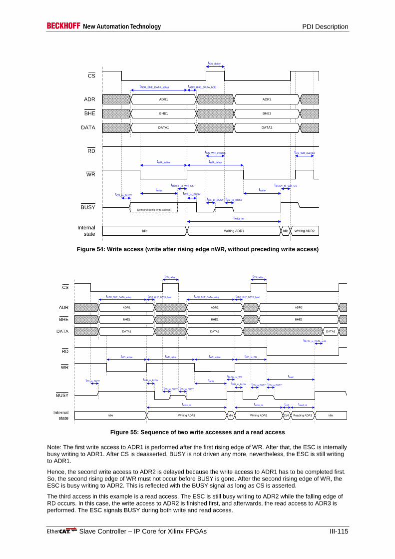
PDI Description
Slave Controller – IP Core for Xilinx FPGAs III-115
BHE1
CS
BHE
WR
RD
DATA
BUSY
ADR1ADR
tWR_active
tCS_delay
tWR_delay
tADR_BHE_DATA_hold
DATA1
tADR_BHE_DATA_setup
tCS_to_BUSY
(with preceding write access)
tWR_to_BUSY
twrite
tCS_to_BUSYtCS_to_BUSY
tBUSY_to_WR_CS
Internal
stateWriting ADR1Idle Idle
tCS_WR_overlap
twrite_int
Writing ADR2
twrite
BHE2
ADR2
DATA2
tBUSY_to_WR_CS
tCS_WR_overlap
Figure 54: Write access (write after rising edge nWR, without preceding write access)
BHE1
CS
BHE
WR
RD
DATA
BUSY
ADR1ADR
tWR_active
tWR_to_BUSY
tCS_delay
tWR_delay
tADR_BHE_DATA_hold
DATA1
tADR_BHE_DATA_setup
twrite_int
tCS_to_BUSY
tCS_to_BUSYtCS_to_BUSY
Internal
stateWriting ADR1
BHE2
ADR2
tWR_active
tWR_to_BUSY
tBUSY_to_WR
tCS_delay
tADR_BHE_DATA_hold
DATA2
tADR_BHE_DATA_setup
tread
ADR3
BHE3
tCS_to_BUSYtCS_to_BUSY
Idle Writing ADR2 Reading ADR3
DATA3
Idle Idle
twrite
twrite_int
tWR_to_RD
tread_int
tBUSY_to_DATA_valid
Coll.
tcoll
Figure 55: Sequence of two write accesses and a read access
Note: The first write access to ADR1 is performed after the first rising edge of WR. After that, the ESC is internally busy writing to ADR1. After CS is deasserted, BUSY is not driven any more, nevertheless, the ESC is still writing to ADR1.
Hence, the second write access to ADR2 is delayed because the write access to ADR1 has to be completed first. So, the second rising edge of WR must not occur before BUSY is gone. After the second rising edge of WR, the ESC is busy writing to ADR2. This is reflected with the BUSY signal as long as CS is asserted.
The third access in this example is a read access. The ESC is still busy writing to ADR2 while the falling edge of RD occurs. In this case, the write access to ADR2 is finished first, and afterwards, the read access to ADR3 is performed. The ESC signals BUSY during both write and read access.
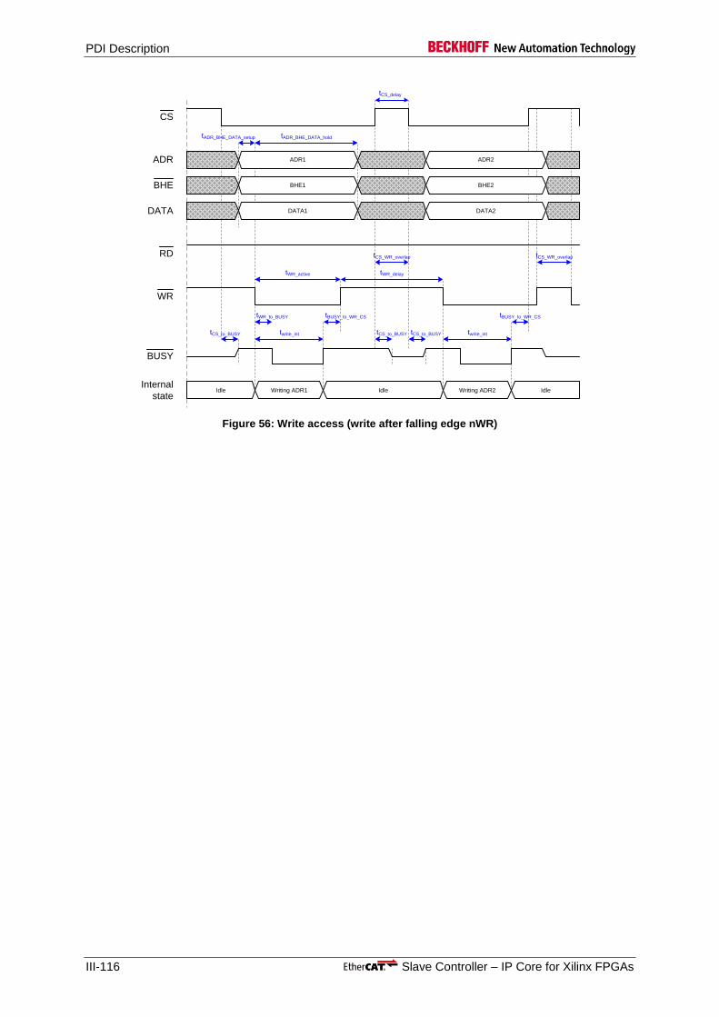
PDI Description
III-116 Slave Controller – IP Core for Xilinx FPGAs
BHE1
CS
BHE
WR
RD
DATA
BUSY
ADR1ADR
tWR_active
tCS_delay
tWR_delay
tADR_BHE_DATA_hold
DATA1
tADR_BHE_DATA_setup
tCS_to_BUSY
tWR_to_BUSY
tCS_to_BUSYtCS_to_BUSY
tBUSY_to_WR_CS
Internal
stateWriting ADR1Idle Idle
tCS_WR_overlap
twrite_int
Writing ADR2
BHE2
ADR2
DATA2
tBUSY_to_WR_CS
tCS_WR_overlap
Idle
twrite_int
Figure 56: Write access (write after falling edge nWR)

PDI Description
Slave Controller – IP Core for Xilinx FPGAs III-117
10.4 PLB Slave Interface
10.4.1 Interface
The PLB v4.6 slave PDI is selected during the IP Core configuration. The main signals of the PLB interface are12:
EtherCAT
IP core
PLB_Abus[0:31]
PLB_masterID[0:x]
PLB_RNW
PLB_BE[0:3]
PLB_size[0:3]
PLB_Sl_addrAck
PLB_PAValid
PLB_Sl_wait
PLB_SPLB_CLK
PLB_Sl_wrComp
PLB_Sl_wrDAck
PLB_Sl_rdDBus[0:31]
PLB_Sl_rdDAck
PLB_wrDBus[0:31]
PLB_Sl_Mbusy[0:x]
PLB_Sl_rdComp
PLB_IRQ_MAIN
PLB_SPLB_Rst
Figure 57: PLB signals
Table 58: PLB signals
Signal Direction Description Signal polarity
PLB_SPLB_Clk IN PLB bus clock
PLB_SPLB_Rst IN PLB reset act. high
PLB_ABus[0:31] IN PLB address bus
PLB_PAValid IN PLB primary address valid act. high
PLB_masterID [0:PLB_MID_WIDTH-1]
IN PLB current master identifier
PLB_RNW IN PLB read not write 0: Write 1: Read
PLB_BE[0:3] IN PLB byte enable
PLB_size[0:3] IN PLB transfer size (must be 0000)
PLB_wrDBus[0:31] IN PLB write data bus
PLB_Sl_addrAck OUT Slave address acknowledge act. high
PLB_Sl_wait OUT Slave wait act. high
PLB_Sl_wrDAck OUT Slave write data acknowledge act. high
PLB_Sl_wrComp OUT Slave write transfer complete act. high
PLB_Sl_rdDBus[0:31] OUT Slave read data bus
PLB_Sl_rdDAck OUT Slave read data acknowledge act. high
PLB_Sl_rdComp OUT Slave read transfer complete act. high
PLB_Sl_MBusy [0: SPLB_NUM_MASTERS-1]
OUT Slave busy
12 The prefix `PDI_` is added to the PLB interface signals for the IP Core interface. Additional signals are part of the PLB interface, but they are not used according to Xilinx PLB v4.6 interface simplifications.
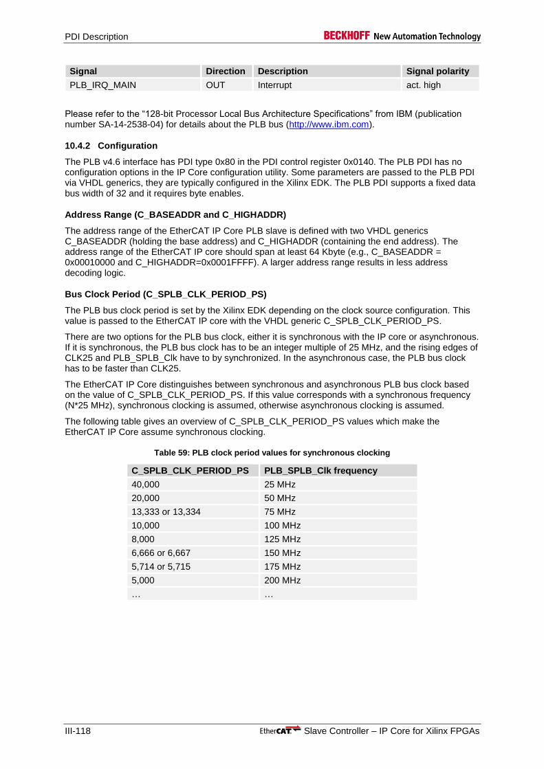
PDI Description
III-118 Slave Controller – IP Core for Xilinx FPGAs
Signal Direction Description Signal polarity
PLB_IRQ_MAIN OUT Interrupt act. high
Please refer to the “128-bit Processor Local Bus Architecture Specifications” from IBM (publication number SA-14-2538-04) for details about the PLB bus (http://www.ibm.com).
10.4.2 Configuration
The PLB v4.6 interface has PDI type 0x80 in the PDI control register 0x0140. The PLB PDI has no configuration options in the IP Core configuration utility. Some parameters are passed to the PLB PDI via VHDL generics, they are typically configured in the Xilinx EDK. The PLB PDI supports a fixed data bus width of 32 and it requires byte enables.
Address Range (C_BASEADDR and C_HIGHADDR)
The address range of the EtherCAT IP Core PLB slave is defined with two VHDL generics C_BASEADDR (holding the base address) and C_HIGHADDR (containing the end address). The address range of the EtherCAT IP core should span at least 64 Kbyte (e.g., C_BASEADDR = 0x00010000 and C_HIGHADDR=0x0001FFFF). A larger address range results in less address decoding logic.
Bus Clock Period (C_SPLB_CLK_PERIOD_PS)
The PLB bus clock period is set by the Xilinx EDK depending on the clock source configuration. This value is passed to the EtherCAT IP core with the VHDL generic C_SPLB_CLK_PERIOD_PS.
There are two options for the PLB bus clock, either it is synchronous with the IP core or asynchronous. If it is synchronous, the PLB bus clock has to be an integer multiple of 25 MHz, and the rising edges of CLK25 and PLB_SPLB_Clk have to by synchronized. In the asynchronous case, the PLB bus clock has to be faster than CLK25.
The EtherCAT IP Core distinguishes between synchronous and asynchronous PLB bus clock based on the value of C_SPLB_CLK_PERIOD_PS. If this value corresponds with a synchronous frequency (N*25 MHz), synchronous clocking is assumed, otherwise asynchronous clocking is assumed.
The following table gives an overview of C_SPLB_CLK_PERIOD_PS values which make the EtherCAT IP Core assume synchronous clocking.
Table 59: PLB clock period values for synchronous clocking
C_SPLB_CLK_PERIOD_PS PLB_SPLB_Clk frequency
40,000 25 MHz
20,000 50 MHz
13,333 or 13,334 75 MHz
10,000 100 MHz
8,000 125 MHz
6,666 or 6,667 150 MHz
5,714 or 5,715 175 MHz
5,000 200 MHz
… …

PDI Description
Slave Controller – IP Core for Xilinx FPGAs III-119
10.4.3 Timing specifications
Table 60: PLB timing characteristics
Parameter Min Max Comment
PRELIMINARY TIMING
tClk x13 40 ns PLB bus clock (fClk ≥25 MHz)
tRead
a) 4* tCLK
+160 ns +x15
b) 6.5 * tCLK
+260 ns +x15
a) 3* tCLK
+200 ns +x15
b) 5.5 * tCLK
+300 ns +x15
32 Bit read access time
a) synchronous (N=1-31)
b) asynchronous
tWrite
a) 4* tCLK +x15
b) 6.5 * tCLK
+100 ns +x15
a) 200 ns +x15
b) 2.5 * tCLK
+300 ns +x15
32 Bit write access time
a) synchronous (N=1-31)
b) asynchronous
13 EtherCAT IP Core: time depends on synthesis results
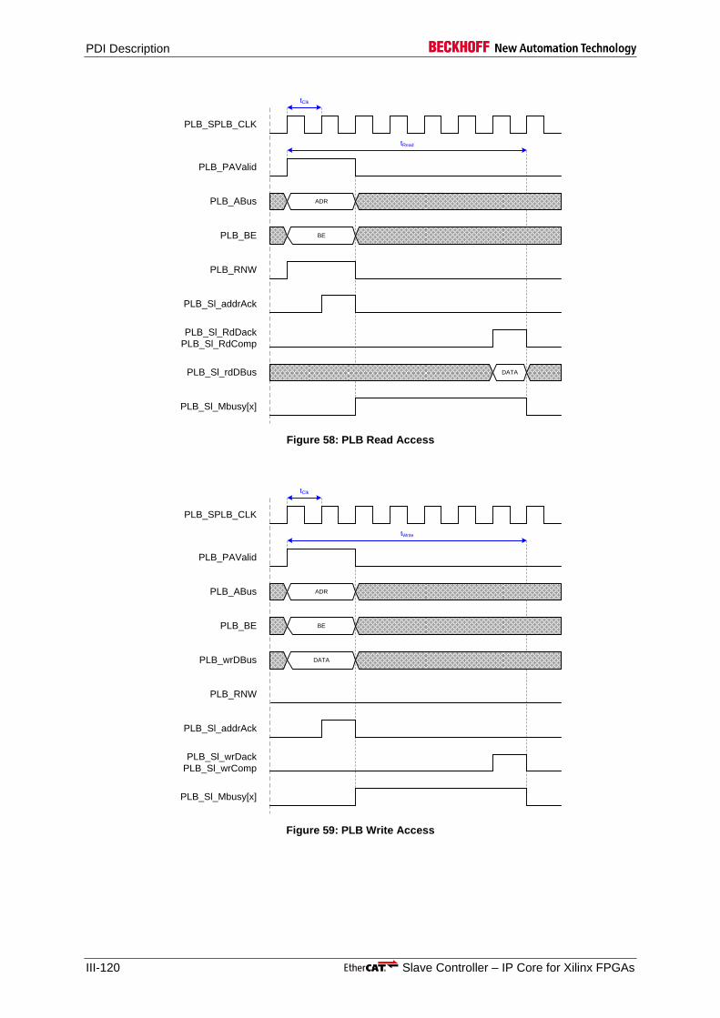
PDI Description
III-120 Slave Controller – IP Core for Xilinx FPGAs
PLB_SPLB_CLK
PLB_ABus ADR
PLB_RNW
PLB_Sl_RdDack
PLB_Sl_RdComp
PLB_Sl_rdDBus DATA
tRead
PLB_PAValid
tClk
PLB_Sl_addrAck
PLB_BE BE
PLB_Sl_Mbusy[x]
Figure 58: PLB Read Access
PLB_SPLB_CLK
PLB_ABus ADR
PLB_RNW
PLB_Sl_wrDack
PLB_Sl_wrComp
tWrite
PLB_PAValid
tClk
PLB_Sl_addrAck
PLB_BE BE
PLB_Sl_Mbusy[x]
PLB_wrDBus DATA
Figure 59: PLB Write Access
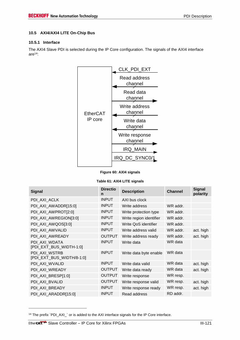
PDI Description
Slave Controller – IP Core for Xilinx FPGAs III-121
10.5 AXI4/AXI4 LITE On-Chip Bus
10.5.1 Interface
The AXI4 Slave PDI is selected during the IP Core configuration. The signals of the AXI4 interface are14:
EtherCAT
IP core
CLK_PDI_EXT
Read address
channel
Read data
channel
Write address
channel
Write data
channel
Write response
channel
IRQ_MAIN
IRQ_DC_SYNC0/1
Figure 60: AXI4 signals
Table 61: AXI4 LITE signals
Signal Direction
Description Channel Signal polarity
PDI_AXI_ACLK INPUT AXI bus clock
PDI_AXI_AWADDR[15:0] INPUT Write address WR addr.
PDI_AXI_AWPROT[2:0] INPUT Write protection type WR addr.
PDI_AXI_AWREGION[3:0] INPUT Write region identifier WR addr.
PDI_AXI_AWQOS[3:0] INPUT Write QoS identifier WR addr.
PDI_AXI_AWVALID INPUT Write address valid WR addr. act. high
PDI_AXI_AWREADY OUTPUT Write address ready WR addr. act. high
PDI_AXI_WDATA [PDI_EXT_BUS_WIDTH-1:0]
INPUT Write data WR data
PDI_AXI_WSTRB [PDI_EXT_BUS_WIDTH/8-1:0]
INPUT Write data byte enable WR data
PDI_AXI_WVALID INPUT Write data valid WR data act. high
PDI_AXI_WREADY OUTPUT Write data ready WR data act. high
PDI_AXI_BRESP[1:0] OUTPUT Write response WR resp.
PDI_AXI_BVALID OUTPUT Write response valid WR resp. act. high
PDI_AXI_BREADY INPUT Write response ready WR resp. act. high
PDI_AXI_ARADDR[15:0] INPUT Read address RD addr.
14 The prefix `PDI_AXI_` or is added to the AXI interface signals for the IP Core interface.
PDI Description
III-122 Slave Controller – IP Core for Xilinx FPGAs
Signal Direction
Description Channel Signal polarity
PDI_AXI_ARPROT[2:0] INPUT Read protection type RD addr.
PDI_AXI_ARREGION[3:0] INPUT Read region identifier RD addr.
PDI_AXI_ARQOS[3:0] INPUT Read QoS identifier RD addr.
PDI_AXI_ARVALID INPUT Read address valid RD addr. act. high
PDI_AXI_ARREADY OUTPUT Read address ready RD addr. act. high
PDI_AXI_RDATA [PDI_EXT_BUS_WIDTH-1:0]
OUTPUT Read data RD data
PDI_AXI_RRESP[1:0] OUTPUT Read response RD data
PDI_AXI_RVALID OUTPUT Read data valid RD data act. high
PDI_AXI_RREADY INPUT Read data ready RD data act. high
PDI_AXI_IRQ_MAIN OUTPUT Interrupt
Table 62: Additional AXI4 signals
Signal Direction
Description Channel Signal polarity
PDI_AXI_AWID [PDI_BUS_ID_WIDTH-1:0]
INPUT Write address ID WR addr.
PDI_AXI_AWLEN[7:0] INPUT Write length WR addr.
PDI_AXI_AWSIZE[2:0] INPUT Write size WR addr.
PDI_AXI_AWBURST[1:0] INPUT Write burst type WR addr.
PDI_AXI_AWLOCK INPUT Write lock WR addr.
PDI_AXI_AWCACHE[3:0] INPUT Write cache type WR addr.
PDI_AXI_WLAST INPUT Write data last WR data act. high
PDI_AXI_BID [PDI_BUS_ID_WIDTH-1:0]
OUTPUT Write response ID WR resp.
PDI_AXI_ARID [PDI_BUS_ID_WIDTH-1:0]
INPUT Read address ID RD addr.
PDI_AXI_ARLEN[7:0] INPUT Read length RD addr.
PDI_AXI_ARSIZE[2:0] INPUT Read size RD addr.
PDI_AXI_ARBURST[1:0] INPUT Read burst type RD addr.
PDI_AXI_ARLOCK INPUT Read lock RD addr.
PDI_AXI_ARCACHE[3:0] INPUT Read cache type RD addr.
PDI_AXI_RID [PDI_BUS_ID_WIDTH-1:0]
OUTPUT Read data ID RD data
PDI_AXI_RLAST OUTPUT Read data last RD data act. high
Please refer to the AMBA AXI and ACE Protocol Specification from ARM® for details about the AXI4/AXI4 LITE bus (http://www.arm.com).
PDI Description
Slave Controller – IP Core for Xilinx FPGAs III-123
10.5.2 Configuration
The AXI4 interface has PDI type 0x80 in the PDI control register 0x0140. The on-chip bus subtype is “001” for AXI4 and “010” for AXI4LITE in the PDI on-chip bus extended configuration register 0x0152:0x0153. The AXI clock speed, data bus width, and ID width are by generics.
Device emulation
Enable Device emulation (0x0141[0]=1). This feature should be disabled in most use cases, since the processor will handle the EtherCAT state machine.
On-chip Bus CLK
The AXI bus clock period can be selected from a wide range. Nevertheless, configuring the bus clock to be a multiple of 25 MHz will result in best performance:
AXI bus clock frequency = N * 25 MHz (N=1...31)
The maximum clock speed depends on the FPGA and the synthesis. The rising edge of AXI clock has to be synchronous with the rising edge of CLK25 of the EtherCAT IP Core (otherwise the bus clock is asynchronous).
On-chip Bus CLK is asynchronous to CLK25 core clock
Select this option if the bus clock is asynchronous and synchronization is required (results in extra delay).
10.5.3 Interrupts
The AXI Slave interface supports up to 3 interrupts for easy connection embedded systems:
the global PDI interrupt (IRQ_MAIN)
IRQ_DC_SYNC0 and IRQ_DC_SYNC1. These interrupts are available if DC is selected. The DC SyncSignals are also available as standard DC Sync0/1 signals.
PDI Description
III-124 Slave Controller – IP Core for Xilinx FPGAs
10.5.4 Timing specifications
The AXI PDI accepts read and write accesses simultaneously. Nevertheless, the AXI PDI is internally restricted to perform one access in a single clock cycle (either read or write). Simultaneous read and write accesses are internally serialized to meet this requirement. The worst case timing increases in this situation as indicated in the AXI timing characteristics. In other words, the internal bandwidth is shared between read and write channel if both make accesses simultaneously. If only one channel is used, it gets the full bandwidth.
Table 63: AXI timing characteristics
Parameter Min Max Comment
PRELIMINARY TIMING
D 8, 16, 32, or 64 AXI data bus width (in Bits)
N 1 31 AXI bus clock factor (if bus clock is a multiple of 25 MHz)
tClk x15 40 ns AXI bus clock period CLK_PDI_EXT
tRead
tWrite
a) tCLK
+D * 5 ns +x15
b) 3.5 * tCLK
+D * 5 ns +100 ns +x15
a) 40 ns +D * 5 ns +x15
b) 3.5 * tCLK
+D * 5 ns +180 ns +x15
c) 40 ns +D * 10 ns +x15
d) 3.5 * tCLK
+D * 10 ns +180 ns +x15
Aligned read/write access time
a) synchronous (N=1-31), read only or write only
b) asynchronous, read only or write only
c) synchronous (N=1-31), simultaneous read and write
d) asynchronous, simultaneous read and write
BW int 25 Mbyte/s Internal PDI bandwidth limit for the sum of read and write accesses
15 EtherCAT IP Core: time depends on synthesis results

PDI Description
Slave Controller – IP Core for Xilinx FPGAs III-125
CLK_PDI_EXT
ARREADY
ADRARADR
RVALID
RDATA DATA
tRead
ARVALID
tClk
Figure 61: AXI Read Access
CLK_PDI_EXT
AWREADY
WREADY
ADR
DATA
AWADR
WDATA
BVALID
tWrite
AWVALID
WVALID
tClk
Figure 62: AXI Write Access

Distributed Clocks SYNC/LATCH Signals
III-126 Slave Controller – IP Core for Xilinx FPGAs
11 Distributed Clocks SYNC/LATCH Signals
For details about the Distributed Clocks refer to Section I.
11.1 Signals
The Distributed Clocks unit of the IP Core has the following external signals (depending on the ESC configuration):
EtherCAT
device LATCH_IN0
SYNC_OUT1
SYNC_OUT0
LATCH_IN1
Figure 63: Distributed Clocks signals
Table 64: Distributed Clocks signals
Signal Direction Description
SYNC_OUT0/1 OUT SyncSignals (alias SYNC[1:0])
LATCH_IN0/1 IN LatchSignals (alias LATCH[1:0])
NOTE: SYNC_OUT0/1 are active high/push-pull outputs.
11.2 Timing specifications
Table 65: DC SYNC/LATCH timing characteristics IP Core
Parameter Min Max Comment
tDC_LATCH 12 ns + x16 Time between Latch0/1 events
tDC_SYNC_Jitter 11 ns + x3 SYNC0/1 output jitter
tDC_SYNC_IRQ_pulse_width 40 ns SYNC0/1 pulse width if the SYNC0/1 signal is used as AL event request (PDI interrupt) signal (masked by register 0x0220 ff.), and if acknowledge mode is not used.
LATCH0/1
tDC_LATCH tDC_LATCH
Figure 64: LatchSignal timing
SYNC0/1
tDC_SYNC_Jitter
Output event time
tDC_SYNC_Jitter
Figure 65: SyncSignal timing
16 EtherCAT IP Core: time depends on synthesis results
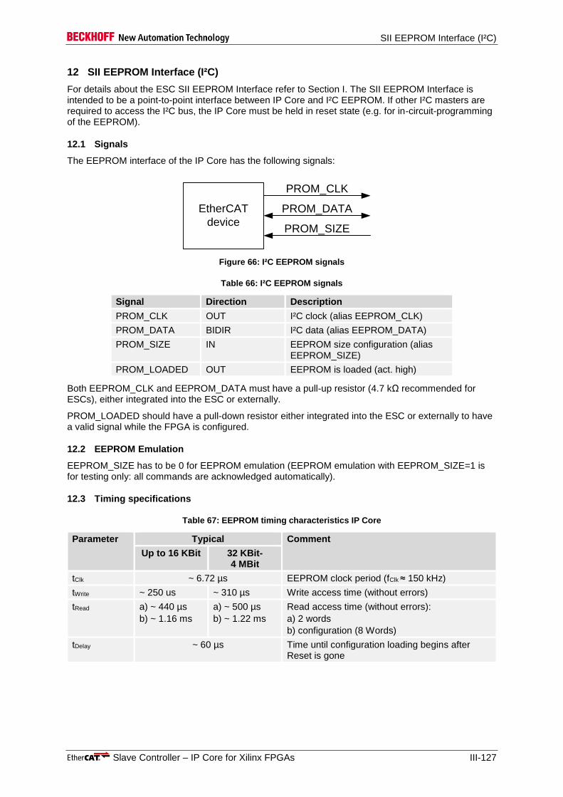
SII EEPROM Interface (I²C)
Slave Controller – IP Core for Xilinx FPGAs III-127
12 SII EEPROM Interface (I²C)
For details about the ESC SII EEPROM Interface refer to Section I. The SII EEPROM Interface is intended to be a point-to-point interface between IP Core and I²C EEPROM. If other I²C masters are required to access the I²C bus, the IP Core must be held in reset state (e.g. for in-circuit-programming of the EEPROM).
12.1 Signals
The EEPROM interface of the IP Core has the following signals:
EtherCAT
device
PROM_DATA
PROM_CLK
PROM_SIZE
Figure 66: I²C EEPROM signals
Table 66: I²C EEPROM signals
Signal Direction Description
PROM_CLK OUT I²C clock (alias EEPROM_CLK)
PROM_DATA BIDIR I²C data (alias EEPROM_DATA)
PROM_SIZE IN EEPROM size configuration (alias EEPROM_SIZE)
PROM_LOADED OUT EEPROM is loaded (act. high)
Both EEPROM_CLK and EEPROM_DATA must have a pull-up resistor (4.7 kΩ recommended for ESCs), either integrated into the ESC or externally.
PROM_LOADED should have a pull-down resistor either integrated into the ESC or externally to have a valid signal while the FPGA is configured.
12.2 EEPROM Emulation
EEPROM_SIZE has to be 0 for EEPROM emulation (EEPROM emulation with EEPROM_SIZE=1 is for testing only: all commands are acknowledged automatically).
12.3 Timing specifications
Table 67: EEPROM timing characteristics IP Core
Parameter Typical Comment
Up to 16 KBit 32 KBit- 4 MBit
tClk ~ 6.72 µs EEPROM clock period (fClk ≈ 150 kHz)
tWrite ~ 250 us ~ 310 µs Write access time (without errors)
tRead a) ~ 440 µs
b) ~ 1.16 ms
a) ~ 500 µs
b) ~ 1.22 ms
Read access time (without errors):
a) 2 words
b) configuration (8 Words)
tDelay ~ 60 µs Time until configuration loading begins after Reset is gone
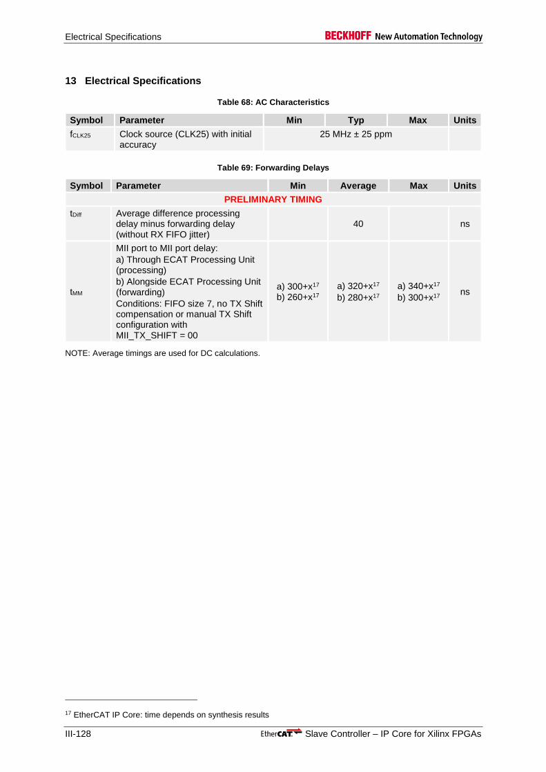
Electrical Specifications
III-128 Slave Controller – IP Core for Xilinx FPGAs
13 Electrical Specifications
Table 68: AC Characteristics
Symbol Parameter Min Typ Max Units
fCLK25 Clock source (CLK25) with initial accuracy
25 MHz ± 25 ppm
Table 69: Forwarding Delays
Symbol Parameter Min Average Max Units
PRELIMINARY TIMING
tDiff Average difference processing delay minus forwarding delay (without RX FIFO jitter)
40 ns
tMM
MII port to MII port delay:
a) Through ECAT Processing Unit (processing)
b) Alongside ECAT Processing Unit (forwarding)
Conditions: FIFO size 7, no TX Shift compensation or manual TX Shift configuration with MII_TX_SHIFT = 00
a) 300+x17 b) 260+x17
a) 320+x17
b) 280+x17
a) 340+x17
b) 300+x17 ns
NOTE: Average timings are used for DC calculations.
17 EtherCAT IP Core: time depends on synthesis results

Synthesis Constraints
Slave Controller – IP Core for Xilinx FPGAs III-129
14 Synthesis Constraints
The following table contains basic IP Core constraints. Refer to Xilinx for details about RGMII constraining.
Table 70: EtherCAT IP Core constraints
Signal Requirement Value Clock reference Description
CLK25 period 40 ns Reference clock (25 MHz)
CLK25_2NS a) period
b) phase shift
a) 40 ns
b) 2 ns CLK25
Derived clock (25 MHz). Phase shift is rising edge CLK25 to rising edge CLK25_2NS.
CLK50 a) period
b) phase shift
a) 20 ns
b) 0 ns CLK25
Derived clock (50 MHz). Phase shift is rising edge to rising edge.
CLK100 a) period
b) phase shift
a) 10 ns
b) 0 ns CLK25
Derived clock (100 MHz). Phase shift is rising edge to rising edge.
nRESET Ignore timing nRESET is asynchronous to any clock
MCLK min. period 400 ns IEEE802.3 requirement (2.5 MHz)
MDIO
a) setup
b) hold
at PHY input
a) 10 ns
b) 10 ns
MCLK (rising edge)
MDIO is changed with falling edge of MCLK, max. output skew of MCLK and MDIO is 190 ns. Constraining is usually not required. IEEE802.3 requirement.
MII_RX_CLK0-2 period 40 ns MII receive reference clock (25 MHz). IEEE802.3 requirement.
MII_RX_DATA0-2[3:0] MII_RX_DV0-2 MII_RX_ERR0-2
a) setup
b) hold
a) 10 ns
b) 10 ns
MII_RX_CLK0-2 (rising edge)
IEEE802.3 requirement
MII_TX_CLK0-2 period 40 ns MII transmit reference clock (25 MHz). Only used for automatic TX Shift compensation. IEEE802.3 requirement.
MII_TX_DATA0-2[3:0]
MII_TX_ENA0-2
Clock-to-Pin
a) min
b) max
a) 0 ns
b) 25 ns
TX_CLK0-2 from PHY (rising edge)
IEEE802.3 requirement
Clock-to-Pin
a) min
b) max
a) 0 ns
b) 10 ns
CLK25 (rising edge)
Incomplete alternative to IEEE802.3 requirement, keeps margin if TX Shift has been determined and compensated. Refer to section III for details.
PROM_CLK period App. dep. I²C clock. Actual ESC output clock is 6.72 µs (≈ 150 kHz). Min. 2.5µs (400 Khz) for example I²C EEPROM chip.
PROM_DATA
a) setup
b) hold
a) 250 ns
b) 0 ns
PROM_CLK
a) rising edge
b) falling edge
PROM_DATA is changed in the middle of the low phase of PROM_CLOCK, i.e., max. output skew of PROM_CLK/PROM_DATA is 1.43 µs. Constraining is usually not required. Example I²C EEPROM chip requirement.
RMII_RX_DATA0/1[1:0] RMII_RX_DV0/1 RMII_RX_ERR0/1 RMII_TX_DATA0/1[1:0] RMII_TX_ENA0/1
a) setup
b) hold
a) 4 ns
b) 2 ns
CLK50 (rising edge)
RMII specification requirement
RGMII_RX_CLK0-2 period 40 ns RGMII receive reference clock (25 MHz). RGMII spec. requirement.
RGMII_RX_CTL0-3 RGMII_RX_DATA0-3[3:0]
a) setup
b) hold
a)
b)
RGMII_RX_CLK0-2 (both edges)
Depending on RX_CLK delay option,
RGMII spec. requirement
RGMII_TX_CLK0-2 a) period
b) phase shift
a) 40 ns
b) 2 ns CLK25_2NS
RGMII transmit reference clock (25 MHz), derived from CLK25_2NS. RGMII spec. requirement.
RGMII_TX_CTL0-3 RGMII_TX_DATA0-3[3:0]
Clock-to-Pin
a) min
b) max
a)
b)
RGMII_TX_CLK0-2 (both edges)
Depending on TX_CLK delay option, RGMII spec. requirement
Other signals, especially PDI signals
application dependent
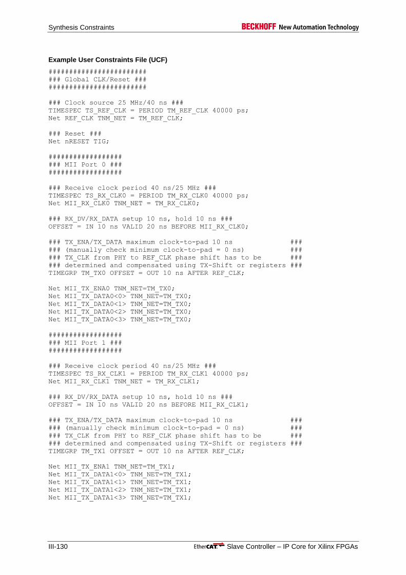
Synthesis Constraints
III-130 Slave Controller – IP Core for Xilinx FPGAs
Example User Constraints File (UCF)
########################
### Global CLK/Reset ###
########################
### Clock source 25 MHz/40 ns ###
TIMESPEC TS_REF_CLK = PERIOD TM_REF_CLK 40000 ps;
Net REF_CLK TNM_NET = TM_REF_CLK;
### Reset ###
Net nRESET TIG;
##################
### MII Port 0 ###
##################
### Receive clock period 40 ns/25 MHz ###
TIMESPEC TS_RX_CLK0 = PERIOD TM_RX_CLK0 40000 ps;
Net MII_RX_CLK0 TNM_NET = TM_RX_CLK0;
### RX_DV/RX_DATA setup 10 ns, hold 10 ns ###
OFFSET = IN 10 ns VALID 20 ns BEFORE MII_RX_CLK0;
### TX_ENA/TX_DATA maximum clock-to-pad 10 ns ###
### (manually check minimum clock-to-pad = 0 ns) ###
### TX_CLK from PHY to REF_CLK phase shift has to be ###
### determined and compensated using TX-Shift or registers ###
TIMEGRP TM_TX0 OFFSET = OUT 10 ns AFTER REF_CLK;
Net MII_TX_ENA0 TNM_NET=TM_TX0;
Net MII_TX_DATA0<0> TNM_NET=TM_TX0;
Net MII_TX_DATA0<1> TNM_NET=TM_TX0;
Net MII_TX_DATA0<2> TNM_NET=TM_TX0;
Net MII_TX_DATA0<3> TNM_NET=TM_TX0;
##################
### MII Port 1 ###
##################
### Receive clock period 40 ns/25 MHz ###
TIMESPEC TS_RX_CLK1 = PERIOD TM_RX_CLK1 40000 ps;
Net MII_RX_CLK1 TNM_NET = TM_RX_CLK1;
### RX_DV/RX_DATA setup 10 ns, hold 10 ns ###
OFFSET = IN 10 ns VALID 20 ns BEFORE MII_RX_CLK1;
### TX_ENA/TX_DATA maximum clock-to-pad 10 ns ###
### (manually check minimum clock-to-pad = 0 ns) ###
### TX_CLK from PHY to REF_CLK phase shift has to be ###
### determined and compensated using TX-Shift or registers ###
TIMEGRP TM_TX1 OFFSET = OUT 10 ns AFTER REF_CLK;
Net MII_TX_ENA1 TNM_NET=TM_TX1;
Net MII_TX_DATA1<0> TNM_NET=TM_TX1;
Net MII_TX_DATA1<1> TNM_NET=TM_TX1;
Net MII_TX_DATA1<2> TNM_NET=TM_TX1;
Net MII_TX_DATA1<3> TNM_NET=TM_TX1;
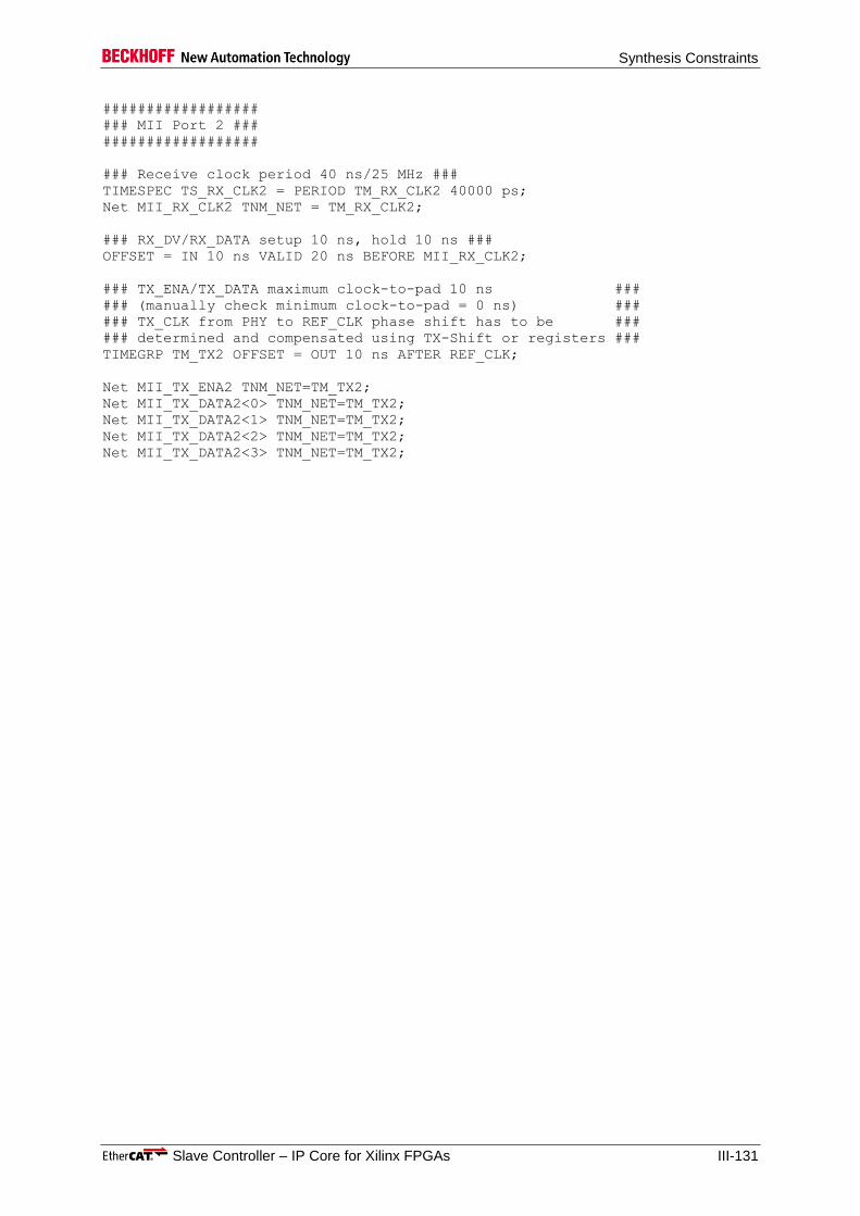
Synthesis Constraints
Slave Controller – IP Core for Xilinx FPGAs III-131
##################
### MII Port 2 ###
##################
### Receive clock period 40 ns/25 MHz ###
TIMESPEC TS_RX_CLK2 = PERIOD TM_RX_CLK2 40000 ps;
Net MII_RX_CLK2 TNM_NET = TM_RX_CLK2;
### RX_DV/RX_DATA setup 10 ns, hold 10 ns ###
OFFSET = IN 10 ns VALID 20 ns BEFORE MII_RX_CLK2;
### TX_ENA/TX_DATA maximum clock-to-pad 10 ns ###
### (manually check minimum clock-to-pad = 0 ns) ###
### TX_CLK from PHY to REF_CLK phase shift has to be ###
### determined and compensated using TX-Shift or registers ###
TIMEGRP TM_TX2 OFFSET = OUT 10 ns AFTER REF_CLK;
Net MII_TX_ENA2 TNM_NET=TM_TX2;
Net MII_TX_DATA2<0> TNM_NET=TM_TX2;
Net MII_TX_DATA2<1> TNM_NET=TM_TX2;
Net MII_TX_DATA2<2> TNM_NET=TM_TX2;
Net MII_TX_DATA2<3> TNM_NET=TM_TX2;

Appendix
III-132 Slave Controller – IP Core for Xilinx FPGAs
15 Appendix
15.1 Support and Service
Beckhoff and our partners around the world offer comprehensive support and service, making available fast and competent assistance with all questions related to Beckhoff products and system solutions.
15.1.1 Beckhoff’s branch offices and representatives
Please contact your Beckhoff branch office or representative for local support and service on Beckhoff products!
The addresses of Beckhoff's branch offices and representatives round the world can be found on her internet pages: http://www.beckhoff.com
You will also find further documentation for Beckhoff components there.
15.2 Beckhoff Headquarters
Beckhoff Automation GmbH & Co. KG Huelshorstweg 20 33415 Verl Germany
Phone: +49 (0) 5246 963-0
Fax: +49 (0) 5246 963-198
E-mail: [email protected]
Web: www.beckhoff.com
Beckhoff Support
Support offers you comprehensive technical assistance, helping you not only with the application of individual Beckhoff products, but also with other, wide-ranging services:
world-wide support
design, programming and commissioning of complex automation systems
and extensive training program for Beckhoff system components
Hotline: +49 (0) 5246 963-157
Fax: +49 (0) 5246 963-9157
E-mail: [email protected]
Beckhoff Service
The Beckhoff Service Center supports you in all matters of after-sales service:
on-site service
repair service
spare parts service
hotline service
Hotline: +49 (0) 5246 963-460
Fax: +49 (0) 5246 963-479
E-mail: [email protected]