vme slave controller module version 1.1 - actel.com · vme slave controller module version 1.1.1...
TRANSCRIPT
Datasheet
VMESmodule
VME Slave Controller Module
Version 1.1.1
INICORE INC. 5600 Mowry School Road Suite 180 Newark, CA 94560t: 510 445 1529 f: 510 656 0995 e: [email protected] www.inicore.com
C O P Y R I G H T © 2 0 1 1 - 2 0 1 2 , I N I C O R E I N C .
V M E S m o d u l e D a t a s h e e t
Tab l e o f C on te n t s
1. OVERVIEW................................................................................................................................... 5
1.1. Features.................................................................................................................................... 5
1.2. Deliverables.............................................................................................................................. 6
1.3. Functional Description............................................................................................................ 6
1.3.1. VME Slave.............................................................................................................................. 6VME Slave Window........................................................................................................................... 7Example............................................................................................................................................ 9
1.3.2. System Failure Diagnostics.................................................................................................. 10
1.3.3. VME Bus Interrupter.............................................................................................................. 10
1.3.4. Local Interrupt Controller....................................................................................................... 11
1.3.5. Control and Status Registers................................................................................................ 11
1.3.6. Mailbox Registers.................................................................................................................. 11
1.3.7. Semaphores.......................................................................................................................... 12
1.3.8. Registers............................................................................................................................... 13Memory Mapping............................................................................................................................ 13Endian Selection............................................................................................................................. 14
1.3.9. Reset Logic........................................................................................................................... 15
2. SIGNAL DESCRIPTION............................................................................................................. 16
2.1. Global Signals........................................................................................................................ 16
2.2. VME Bus Signals.................................................................................................................... 16
2.2.1. VMEbus signals external buffering example......................................................................... 18
2.3. User Side Interfaces............................................................................................................... 18
2.3.1. Special purpose User side Signals....................................................................................... 19
2.3.2. Local Bus Master Port........................................................................................................... 19Local Bus Master Port write cycle................................................................................................... 22Local bus Master Port read cycle.................................................................................................... 22Local bus Master Port read-Modify-Write Cycle............................................................................. 23
Copyright © 2011-2012, Inicore Inc. Indexes - Page II
V M E S m o d u l e D a t a s h e e t
2.3.3. Local Bus Slave Port............................................................................................................. 24Local Bus Slave Port CSR Write Cycle........................................................................................... 25Local Bus Slave Port CSR Read Cycle.......................................................................................... 26
3. CORE CONFIGURATION........................................................................................................... 27
3.1. Rescinding DTACK................................................................................................................ 27
4. PROGRAMMERS GUIDE........................................................................................................... 28
4.1. Internal CSR Memory Space................................................................................................. 28
4.2. Description of Registers....................................................................................................... 29
4.2.1. Device Control Register: DEV_CTRL................................................................................... 29
4.2.2. Slave Access Decoding (1-8): SVL_ACC_DECn................................................................. 30
4.2.3. Slave Access Address Decoder Compare Register (1-8): SLV_ACC_CMPn......................31
4.2.4. Slave Access Address Decoder Mask Register (1-8): SLV_ACC_MSKn............................31
4.2.5. Mailbox Registers (1-4): MAILBOXn..................................................................................... 32
4.2.6. Semaphore Registers (0-3): SEMAPHORE......................................................................... 33
4.2.7. VME Interrupter Map: VINT_MAP......................................................................................... 33
4.2.8. VME Interrupter STATUS/ID: VINT_STATID......................................................................... 34
4.2.9. VME Interrupter Request: VINT_REQ.................................................................................. 34
4.2.10. VME Interrupter Status Register: VINT_STATUS............................................................... 35
4.2.11. VME Interrupter Enable Register: VINT_EBL..................................................................... 35
4.2.12. local Interrupt Status Register: LINT_STATUS................................................................... 36
4.2.13. Local Interrupt Enable Register: LINT_EBL........................................................................ 37
4.2.14. CSR Bit Clear Register: BIT_CLEAR................................................................................. 37
4.2.15. CSR Bit Set Register: BIT_SET.......................................................................................... 38
4.2.16. CSR Base Register: CRBAR.............................................................................................. 39
Copyright © 2011-2012, Inicore Inc. Indexes - Page III
V M E S m o d u l e D a t a s h e e t
F i gur e In d e x
Figure 1: VME Slave Module Block Diagram.................................................................................... 5
Figure 2: VME Slave Windows......................................................................................................... 7
Figure 3: VME Slave Address Space Decoding............................................................................... 8
Figure 4: VME Slave Address Calculation........................................................................................ 9
Figure 5: CR/CSR Memory Mapping.............................................................................................. 13
Figure 6: External VME transceiver connectivity............................................................................ 18
Figure 7: User write cycle with different wait-states........................................................................ 22
Figure 8: User read cycle with different wait-states........................................................................ 22
Figure 9: User read-modify-write cycle........................................................................................... 23
Figure 10: User read-only cycle...................................................................................................... 24
Figure 11: Local bus slave port CSR write timing........................................................................... 25
Figure 12: Local bus slave port CSR read timing........................................................................... 26
D oc u m e n t H i s to r yThe following table gives an overview of the document history and can help in the determination if the latest version of this document has been used.
Version Comment1.0.0 Initial release1.1.0 – Global document update
– Updated bit mapping of slave window configuration register– Increased maximal number of slave windows to 8– Corrected LENDIAN description
1.1.1 – Added GA parity error interrupt
Copyright © 2011-2012, Inicore Inc. Indexes - Page IV
V M E S m o d u l e P R E L I M I N A R Y D a t a s h e e t
1 . Ov e r v i e w
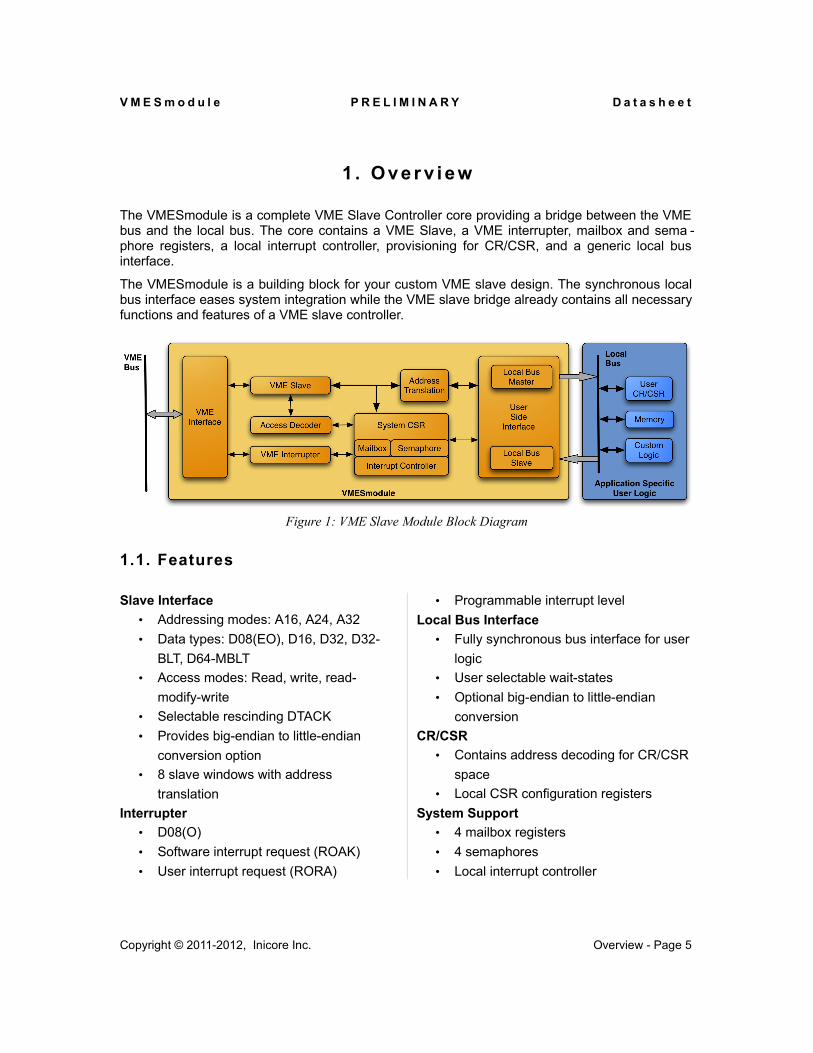
The VMESmodule is a complete VME Slave Controller core providing a bridge between the VME bus and the local bus. The core contains a VME Slave, a VME interrupter, mailbox and sema -phore registers, a local interrupt controller, provisioning for CR/CSR, and a generic local bus interface.
The VMESmodule is a building block for your custom VME slave design. The synchronous local bus interface eases system integration while the VME slave bridge already contains all necessary functions and features of a VME slave controller.
1.1. Features
Slave Interface• Addressing modes: A16, A24, A32• Data types: D08(EO), D16, D32, D32-
BLT, D64-MBLT• Access modes: Read, write, read-
modify-write• Selectable rescinding DTACK• Provides big-endian to little-endian
conversion option• 8 slave windows with address
translationInterrupter
• D08(O)• Software interrupt request (ROAK)• User interrupt request (RORA)
• Programmable interrupt levelLocal Bus Interface
• Fully synchronous bus interface for user logic
• User selectable wait-states• Optional big-endian to little-endian
conversionCR/CSR
• Contains address decoding for CR/CSR space
• Local CSR configuration registersSystem Support
• 4 mailbox registers• 4 semaphores• Local interrupt controller
Copyright © 2011-2012, Inicore Inc. Overview - Page 5
Figure 1: VME Slave Module Block Diagram
V M E S m o d u l e P R E L I M I N A R Y D a t a s h e e t
1.2. Deliverables
• RTL code• Self-verifying system-level testbench• Simulation and synthesis scripts• Synthesis information• Timing constraints• User guide
1.3. Functional Description
1.3.1. VME Slave
Using the VME slave, other VME masters can access the local configuration registers as well as devices and memories connected to the user-side interface. To access the user-side interface, four separate memory windows are available that map a section of the local user-side memory into the VME address space.
The VME slave supports following type of data transfer modes:
• Addressing modes: A16, A24, A32• Data types: D08(EO), D16, D32, D32-BLT, D64-MBLT• Access modes: Read, write, read-modify-write
Copyright © 2011-2012, Inicore Inc. Overview - Page 6
V M E S m o d u l e P R E L I M I N A R Y D a t a s h e e t
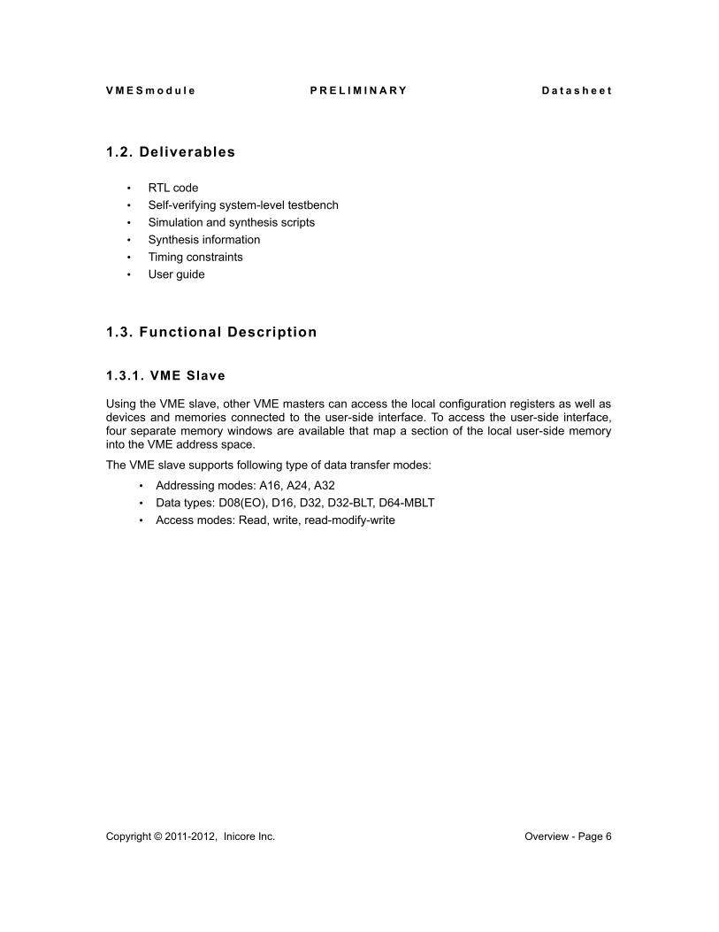
VME Slave Window
The VMESmodule maps eight different VME memory windows into the local user-side memory space:
To detect if a VME slave access matches one of these windows, following tasks are performed:1) The VME address is masked with the VME Address Mask Register (SLVWn_ADEM) and
then compared with the expected VME Address Decode Register (SLVWn_ADER)2) The VME address modifier is compared with the preprogrammed value (SLVWn_AM_xx) 3) The slave address window needs to be enabled (SLVWn_EBL)
For gate-count optimizations, the 4 slave windows can be configured using top-level generics:
Generic Name Description
G_VME_SLVWn_AVn=1..8
Slave window availableFor gate-count optimization, each slave access window can individually disabled.
0: Slave window is not available1: Slave window is available
Copyright © 2011-2012, Inicore Inc. Overview - Page 7
Figure 2: VME Slave Windows
V M E S m o d u l e P R E L I M I N A R Y D a t a s h e e t
Generic Name Description
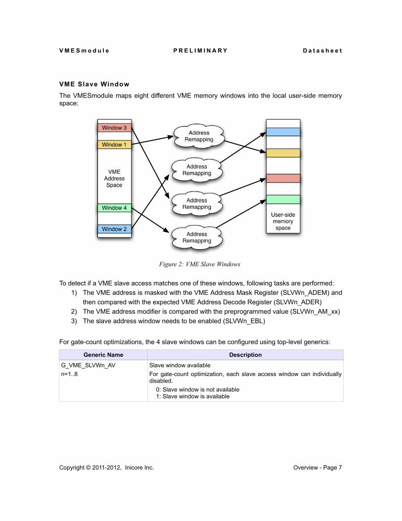
G_VME_SLVWn_SIZEn=1..8
Slave window sizeThe window size is defined as 256 x 2G_VME_SLVWx_SIZE :
0: 256 bytes1: 512 bytes2: 1k bytes…15: 8M bytesOthers: not valid
This decoding procedure is shown in following figure:
Copyright © 2011-2012, Inicore Inc. Overview - Page 8
Figure 3: VME Slave Address Space Decoding
8 7 0
VME Address
31
&8
SLVWn_ADEM
31
8
SLVWn_ADER
31
=
0
VME Address Modifier
5
SLVWn_AM_xx=
SLVWn_EBL
&AddressWindowMatch
Control RegisterVME Bus
V M E S m o d u l e P R E L I M I N A R Y D a t a s h e e t
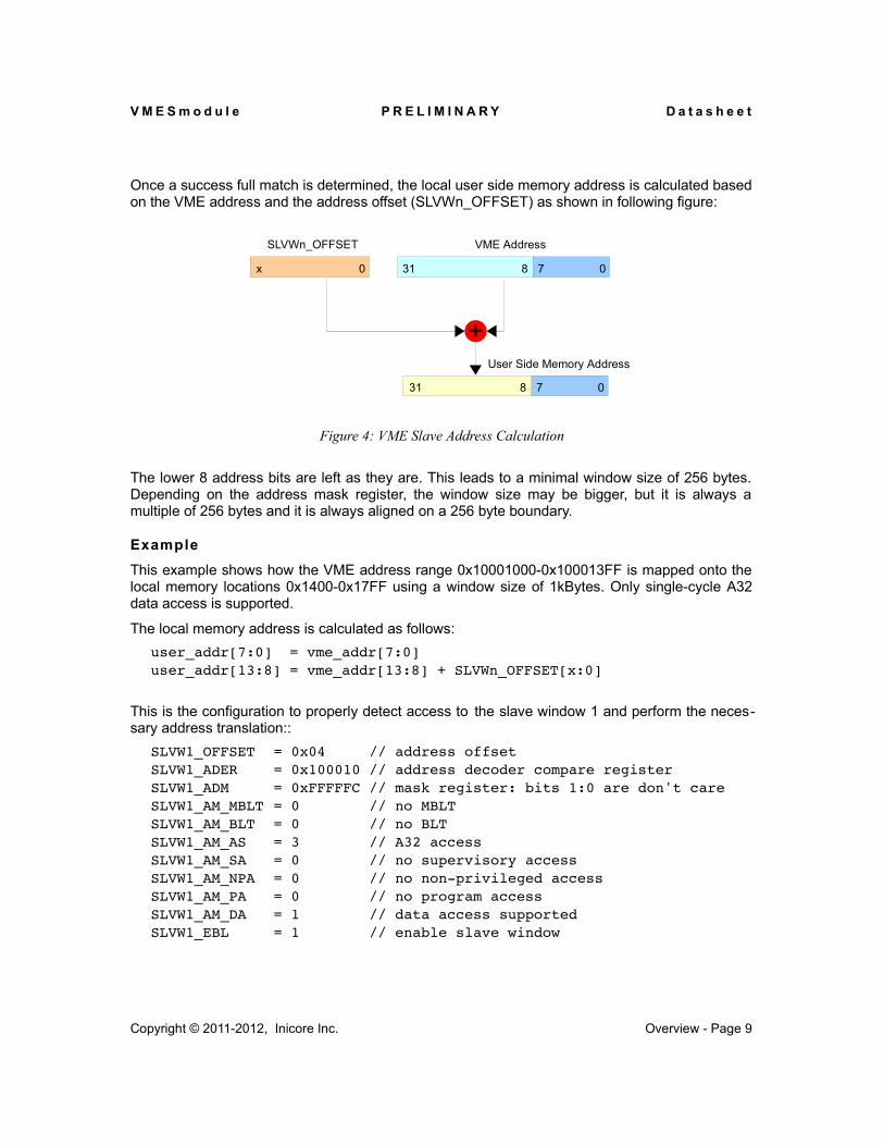
Once a success full match is determined, the local user side memory address is calculated based on the VME address and the address offset (SLVWn_OFFSET) as shown in following figure:
The lower 8 address bits are left as they are. This leads to a minimal window size of 256 bytes. Depending on the address mask register, the window size may be bigger, but it is always a multiple of 256 bytes and it is always aligned on a 256 byte boundary.
Example
This example shows how the VME address range 0x10001000-0x100013FF is mapped onto the local memory locations 0x1400-0x17FF using a window size of 1kBytes. Only single-cycle A32 data access is supported.
The local memory address is calculated as follows:user_addr[7:0] = vme_addr[7:0]user_addr[13:8] = vme_addr[13:8] + SLVWn_OFFSET[x:0]
This is the configuration to properly detect access to the slave window 1 and perform the neces-sary address translation::
SLVW1_OFFSET = 0x04 // address offsetSLVW1_ADER = 0x100010 // address decoder compare registerSLVW1_ADM = 0xFFFFFC // mask register: bits 1:0 are don't careSLVW1_AM_MBLT = 0 // no MBLTSLVW1_AM_BLT = 0 // no BLTSLVW1_AM_AS = 3 // A32 accessSLVW1_AM_SA = 0 // no supervisory accessSLVW1_AM_NPA = 0 // no non-privileged accessSLVW1_AM_PA = 0 // no program accessSLVW1_AM_DA = 1 // data access supportedSLVW1_EBL = 1 // enable slave window
Copyright © 2011-2012, Inicore Inc. Overview - Page 9
Figure 4: VME Slave Address Calculation
31 8 7 0
User Side Memory Address
8 7 0
VME Address
31
+
x 0
SLVWn_OFFSET
V M E S m o d u l e P R E L I M I N A R Y D a t a s h e e t
1.3.2. System Failure Diagnostics
In VME systems SYSFAIL* is used as indicator for ongoing system failure analysis or as an indic -ator of a system failure.
SYSFAIL* can be set and cleared under software control using the SDES bit of the BIT_SET and BIT_CLEAR registers. The user side signal user_sysfail_n is provided for diagnostics. Usually, it drives a status LED to help a visual inspection to determine which board has failed.
A top-level generic is available to set the SYSFAIL* behavior at power-up or system reset:
Generic Name Description
G_SYSFAIL_MODE SYSFAIL* Mode SelectionUpon hardware reset or a system reset, the core can assert SYSFAIL*
0: Do not assert SYSFAIL* upon reset1: Assert SYSFAIL* upon reset
If SYSFAIL* is driven at power-up, it has to be cleared by using the BIT_CLEAR.SDES bit.
1.3.3. VME Bus Interrupter
The VME Bus Interrupter returns the local STATUS/ID vector VINT_STAT during a VME IACK cycle when the interrupt level matches a pending request. There are two possible interrupt request sources:
• Software interruptA software interrupt request is created by setting the VINT_SWREQ bit. This will cause a VME interrupt on the level defined by VINT_SWIRQ. The STATUS/ID returned is the VINT_STAT with the LSB set to zero.The software interrupt is automatically acknowledged during an VME IACK cycle (ROAK) and the local interrupt flag IS_SWIACK is set.
• User interruptBy asserting the input user_vint_req, a VME interrupt is generated. The level is defined by VINT_UIRQ and the STATUS/ID returned is VINT_STAT with the LSB set to one.To acknowledge the user interrupt, the interrupt service routine needs first to acknow -ledge the external interrupt source prior to the acknowledging the VIS_UIRQ flag (RORA).
The VME interrupt request is only generated when the respective interrupt source is enabled by setting its VINT_EBL flag to one.
During the VME interrupt service routine, the VME interrupt handler uses an IACK cycle to access the VME interrupt status register VINT_STATUS to determine the interrupter source and to acknowledge it.
If both a software interrupt and a user interrupt are pending on the same level, then the software interrupt will be acknowledged first.
Copyright © 2011-2012, Inicore Inc. Overview - Page 10
V M E S m o d u l e P R E L I M I N A R Y D a t a s h e e t
1.3.4. Local Interrupt Controller
Several interrupts are generated based upon different local interrupt events. Each interrupt source can be individually enabled.
Interrupt sources:
– Mailbox 0-3 write access
– VME bus error
– AC Fail
– System Fail
– VME software interrupt
– GA*/GAP* parity error
1.3.5. Control And Status Registers
All control and status registers can be accessed either by an external VME master or by the local CPU.
– Access via VMEAll control and status registers are mapped into the CR/CSR space as defined the the VME and VMEx specification.
– Access via local busAll control and status registers are directly accessible using the User CSR Port.
The VMESmodule contains an internal arbiter to protect against data corruption due to concurrent CSR access. Read-modify-write cycles to the CR/CSR memory space are atomic, meaning that access to the same register from the local bus is prevented.
1.3.6. Mailbox Registers
Mailbox registers are used as a communication channel between the VME bus and the local CPU. When an external VME master writes to the user-side memory, he can set a specific code in the mailbox. A write operation will generate an interrupt to the local CPU to indicate that new data is available. Mailboxes can be used as flow control mechanism.
4 separate mailbox registers are available to provide a communication path between the VME bus and the local bus, or vice-versa.
– Read and write access is provided from VME bus and local bus
– Writing to the mailbox register will set the respective irq_mbox[n] interrupt source. If the respective interrupt is enabled, a local bus interrupt is generated.
Copyright © 2011-2012, Inicore Inc. Overview - Page 11
V M E S m o d u l e P R E L I M I N A R Y D a t a s h e e t
1.3.7. Semaphores
The System Controller has 4 semaphore registers. They can be used as access control to common resources such as VME slave memory window.
Each semaphore is 8-bits. Bit 7 is the semaphore bit and the other 7 bits are used as a tag. In order to have semaphores working properly, the system setup needs to guarantee that all tags are unique (eg, not two masters use the same tag!).
Operation:
1) Write new semaphore tag to semaphore register and set bit 7
2) Read back semaphore. If read value matches the requested semaphore tag, the sema -phore is granted. If semaphore is not granted, restart at 1)
3) Normal operation
4) Once the semaphore is not needed anymore, write to semaphore with bit 7 cleared.
The semaphore bit (bit 7) is used as access control. When set, the semaphore is protected from updates. To clear a semaphore, write to it with bit 7 set to zero. Only the port that requested the semaphore my clear it! E.g., if the VME port set the semaphore, only the VME port can clear the semaphore, if the local CPU set the semaphore, only the local CPU may clear it.
Copyright © 2011-2012, Inicore Inc. Overview - Page 12
V M E S m o d u l e P R E L I M I N A R Y D a t a s h e e t
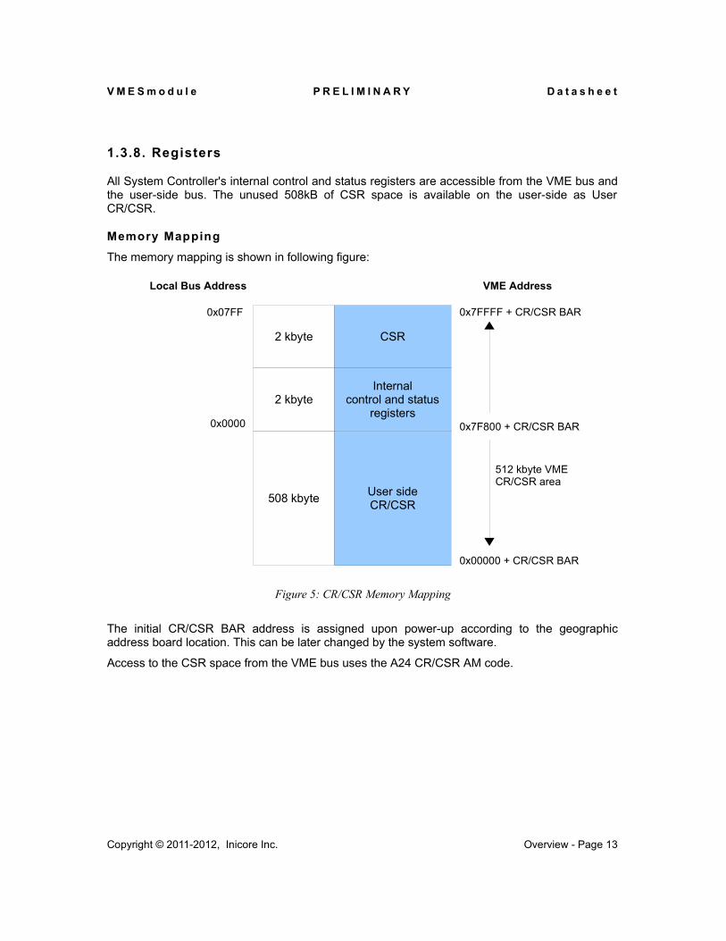
1.3.8. Registers
All System Controller's internal control and status registers are accessible from the VME bus and the user-side bus. The unused 508kB of CSR space is available on the user-side as User CR/CSR.
Memory Mapping
The memory mapping is shown in following figure:
The initial CR/CSR BAR address is assigned upon power-up according to the geographic address board location. This can be later changed by the system software.
Access to the CSR space from the VME bus uses the A24 CR/CSR AM code.
Copyright © 2011-2012, Inicore Inc. Overview - Page 13
Figure 5: CR/CSR Memory Mapping
CSR
Internalcontrol and status
registers
User sideCR/CSR
0x00000 + CR/CSR BAR
0x7FFFF + CR/CSR BAR
2 kbyte
2 kbyte
508 kbyte
VME Address
0x07FF
Local Bus Address
0x0000
512 kbyte VMECR/CSR area
0x7F800 + CR/CSR BAR
V M E S m o d u l e P R E L I M I N A R Y D a t a s h e e t
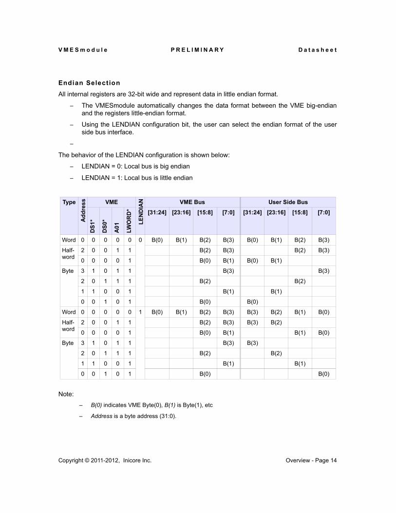
Endian Selection
All internal registers are 32-bit wide and represent data in little endian format.
– The VMESmodule automatically changes the data format between the VME big-endian and the registers little-endian format.
– Using the LENDIAN configuration bit, the user can select the endian format of the user side bus interface.
–
The behavior of the LENDIAN configuration is shown below:
– LENDIAN = 0: Local bus is big endian
– LENDIAN = 1: Local bus is little endian
Type
Add
ress VME
DS1
*
DS0
*
A01
LWO
RD
*
LEN
DIA
N VME Bus User Side Bus
[31:24] [23:16] [15:8] [7:0] [31:24] [23:16] [15:8] [7:0]
Word 0 0 0 0 0
Half- word
2
0
0 0 1 1
0 0 0 1
Byte 3
2
1
0
1 0 1 1
0 1 1 1
1 0 0 1
0 1 0 1
0 B(0) B(1) B(2) B(3) B(0) B(1) B(2) B(3)
B(2) B(3) B(2) B(3)
B(0) B(1) B(0) B(1)
B(3) B(3)
B(2) B(2)
B(1) B(1)
B(0) B(0)
Word 0 0 0 0 0
Half- word
2
0
0 0 1 1
0 0 0 1
Byte 3
2
1
0
1 0 1 1
0 1 1 1
1 0 0 1
0 1 0 1
1 B(0) B(1) B(2) B(3) B(3) B(2) B(1) B(0)
B(2) B(3) B(3) B(2)
B(0) B(1) B(1) B(0)
B(3) B(3)
B(2) B(2)
B(1) B(1)
B(0) B(0)
Note:– B(0) indicates VME Byte(0), B(1) is Byte(1), etc
– Address is a byte address (31:0).
Copyright © 2011-2012, Inicore Inc. Overview - Page 14
V M E S m o d u l e P R E L I M I N A R Y D a t a s h e e t
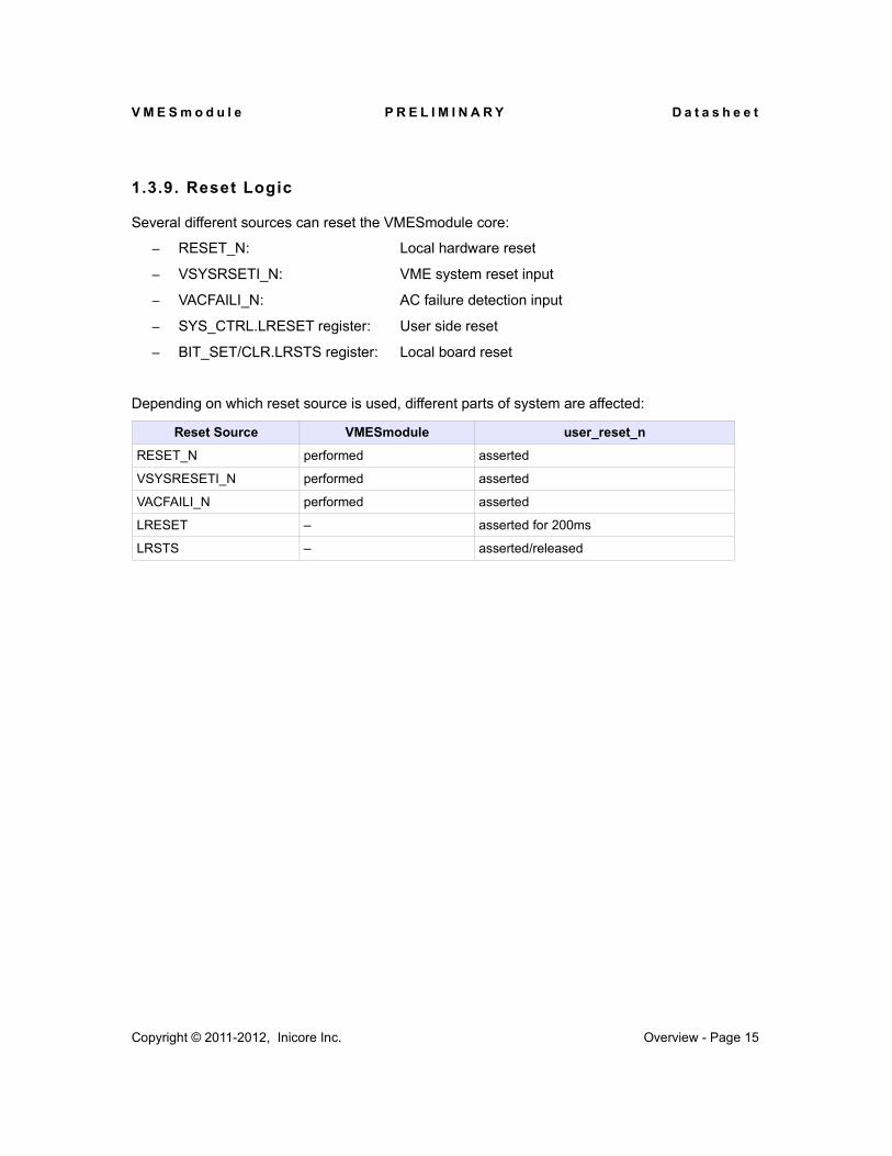
1.3.9. Reset Logic
Several different sources can reset the VMESmodule core:
– RESET_N: Local hardware reset
– VSYSRSETI_N: VME system reset input
– VACFAILI_N: AC failure detection input
– SYS_CTRL.LRESET register: User side reset
– BIT_SET/CLR.LRSTS register: Local board reset
Depending on which reset source is used, different parts of system are affected:
Reset Source VMESmodule user_reset_n
RESET_N performed asserted
VSYSRESETI_N performed asserted
VACFAILI_N performed asserted
LRESET – asserted for 200ms
LRSTS – asserted/released
Copyright © 2011-2012, Inicore Inc. Overview - Page 15
V M E S m o d u l e P R E L I M I N A R Y D a t a s h e e t
2 . S i gn a l D e sc r i p t i o n
This chapter describes all interface signals of the VMESmodule.
2.1. Global Signals
Pin Name Direction Description
CLK_SYS in System clock, 40 MHz or higher
RESET_N in Reset input, asynchronous active low
2.2. VME Bus Signals
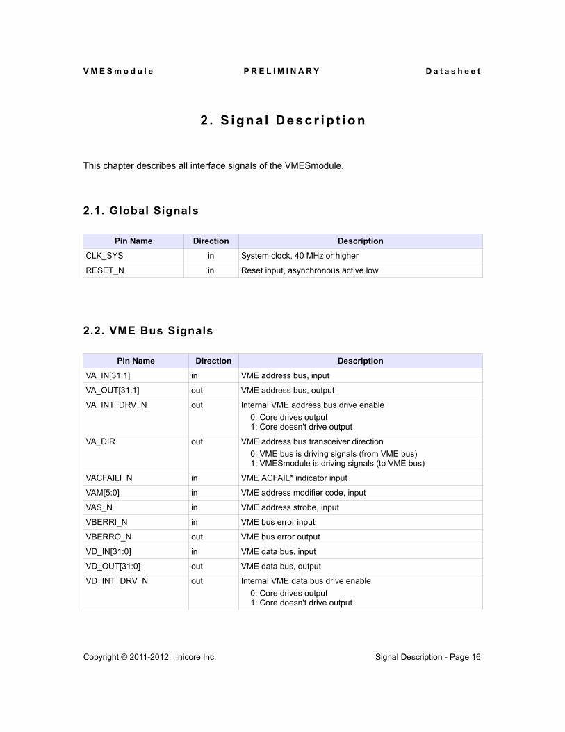
Pin Name Direction Description
VA_IN[31:1] in VME address bus, input
VA_OUT[31:1] out VME address bus, output
VA_INT_DRV_N out Internal VME address bus drive enable0: Core drives output1: Core doesn't drive output
VA_DIR out VME address bus transceiver direction0: VME bus is driving signals (from VME bus)1: VMESmodule is driving signals (to VME bus)
VACFAILI_N in VME ACFAIL* indicator input
VAM[5:0] in VME address modifier code, input
VAS_N in VME address strobe, input
VBERRI_N in VME bus error input
VBERRO_N out VME bus error output
VD_IN[31:0] in VME data bus, input
VD_OUT[31:0] out VME data bus, output
VD_INT_DRV_N out Internal VME data bus drive enable0: Core drives output1: Core doesn't drive output
Copyright © 2011-2012, Inicore Inc. Signal Description - Page 16
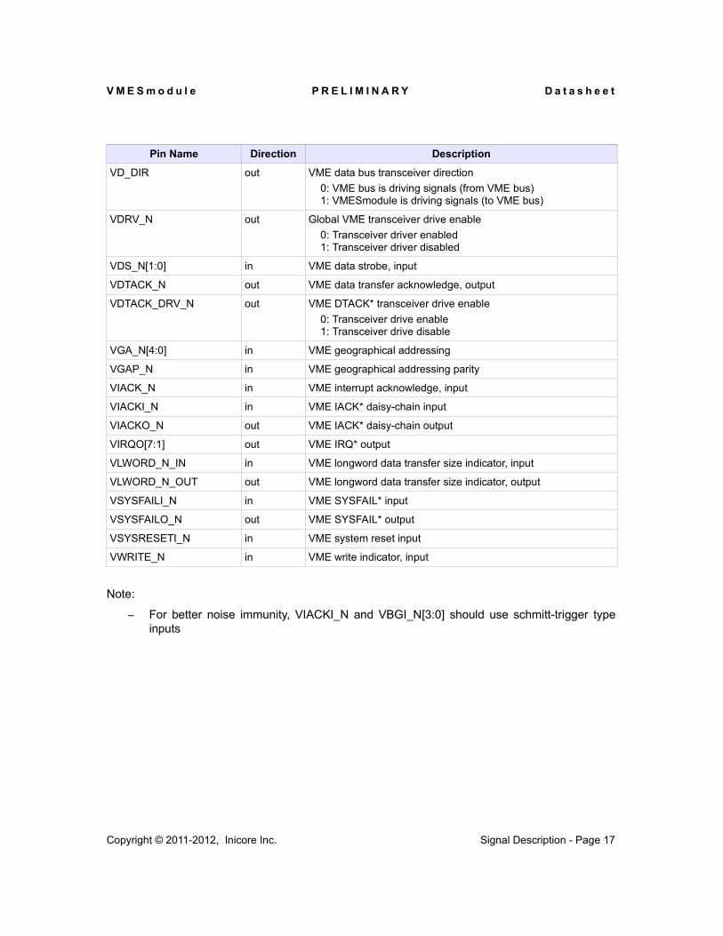
V M E S m o d u l e P R E L I M I N A R Y D a t a s h e e t
Pin Name Direction Description
VD_DIR out VME data bus transceiver direction0: VME bus is driving signals (from VME bus)1: VMESmodule is driving signals (to VME bus)
VDRV_N out Global VME transceiver drive enable0: Transceiver driver enabled1: Transceiver driver disabled
VDS_N[1:0] in VME data strobe, input
VDTACK_N out VME data transfer acknowledge, output
VDTACK_DRV_N out VME DTACK* transceiver drive enable0: Transceiver drive enable1: Transceiver drive disable
VGA_N[4:0] in VME geographical addressing
VGAP_N in VME geographical addressing parity
VIACK_N in VME interrupt acknowledge, input
VIACKI_N in VME IACK* daisy-chain input
VIACKO_N out VME IACK* daisy-chain output
VIRQO[7:1] out VME IRQ* output
VLWORD_N_IN in VME longword data transfer size indicator, input
VLWORD_N_OUT out VME longword data transfer size indicator, output
VSYSFAILI_N in VME SYSFAIL* input
VSYSFAILO_N out VME SYSFAIL* output
VSYSRESETI_N in VME system reset input
VWRITE_N in VME write indicator, input
Note:
– For better noise immunity, VIACKI_N and VBGI_N[3:0] should use schmitt-trigger type inputs
Copyright © 2011-2012, Inicore Inc. Signal Description - Page 17
V M E S m o d u l e P R E L I M I N A R Y D a t a s h e e t
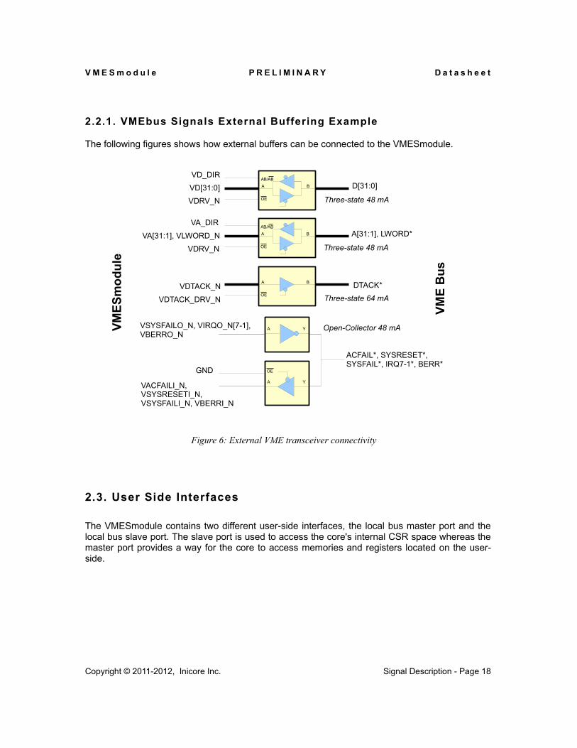
2.2.1. VMEbus Signals External Buffering Example
The following figures shows how external buffers can be connected to the VMESmodule.
2.3. User Side Interfaces
The VMESmodule contains two different user-side interfaces, the local bus master port and the local bus slave port. The slave port is used to access the core's internal CSR space whereas the master port provides a way for the core to access memories and registers located on the user-side.
Copyright © 2011-2012, Inicore Inc. Signal Description - Page 18
Figure 6: External VME transceiver connectivity
VD[31:0] D[31:0]VD_DIR
VDRV_N Three-state 48 mA
BAB/AB
OE
A
VA[31:1], VLWORD_N A[31:1], LWORD*VA_DIR
VDRV_N Three-state 48 mA
BAB/AB
OE
A
VMES
mod
ule
VME
Bus
VDTACK_N DTACK*
VDTACK_DRV_N Three-state 64 mA
B
OE
A
Open-Collector 48 mA
ACFAIL*, SYSRESET*, SYSFAIL*, IRQ7-1*, BERR*
VSYSFAILO_N, VIRQO_N[7-1],VBERRO_N
GND
VACFAILI_N, VSYSRESETI_N, VSYSFAILI_N, VBERRI_N
YA
YA
OE
V M E S m o d u l e P R E L I M I N A R Y D a t a s h e e t
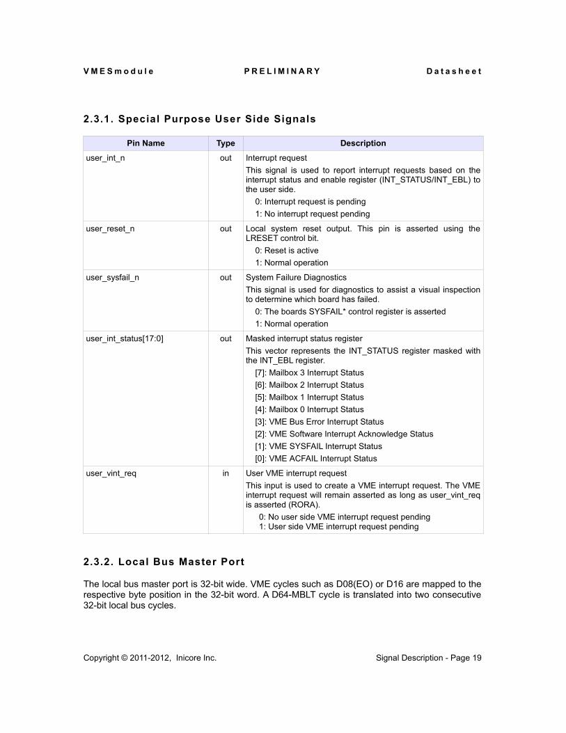
2.3.1. Special Purpose User Side Signals
Pin Name Type Description
user_int_n out Interrupt requestThis signal is used to report interrupt requests based on the interrupt status and enable register (INT_STATUS/INT_EBL) to the user side.
0: Interrupt request is pending1: No interrupt request pending
user_reset_n out Local system reset output. This pin is asserted using the LRESET control bit.
0: Reset is active1: Normal operation
user_sysfail_n out System Failure DiagnosticsThis signal is used for diagnostics to assist a visual inspection to determine which board has failed.
0: The boards SYSFAIL* control register is asserted1: Normal operation
user_int_status[17:0] out Masked interrupt status registerThis vector represents the INT_STATUS register masked with the INT_EBL register.
[7]: Mailbox 3 Interrupt Status [6]: Mailbox 2 Interrupt Status [5]: Mailbox 1 Interrupt Status [4]: Mailbox 0 Interrupt Status[3]: VME Bus Error Interrupt Status[2]: VME Software Interrupt Acknowledge Status[1]: VME SYSFAIL Interrupt Status[0]: VME ACFAIL Interrupt Status
user_vint_req in User VME interrupt requestThis input is used to create a VME interrupt request. The VME interrupt request will remain asserted as long as user_vint_req is asserted (RORA).
0: No user side VME interrupt request pending1: User side VME interrupt request pending
2.3.2. Local Bus Master Port
The local bus master port is 32-bit wide. VME cycles such as D08(EO) or D16 are mapped to the respective byte position in the 32-bit word. A D64-MBLT cycle is translated into two consecutive 32-bit local bus cycles.
Copyright © 2011-2012, Inicore Inc. Signal Description - Page 19
V M E S m o d u l e P R E L I M I N A R Y D a t a s h e e t
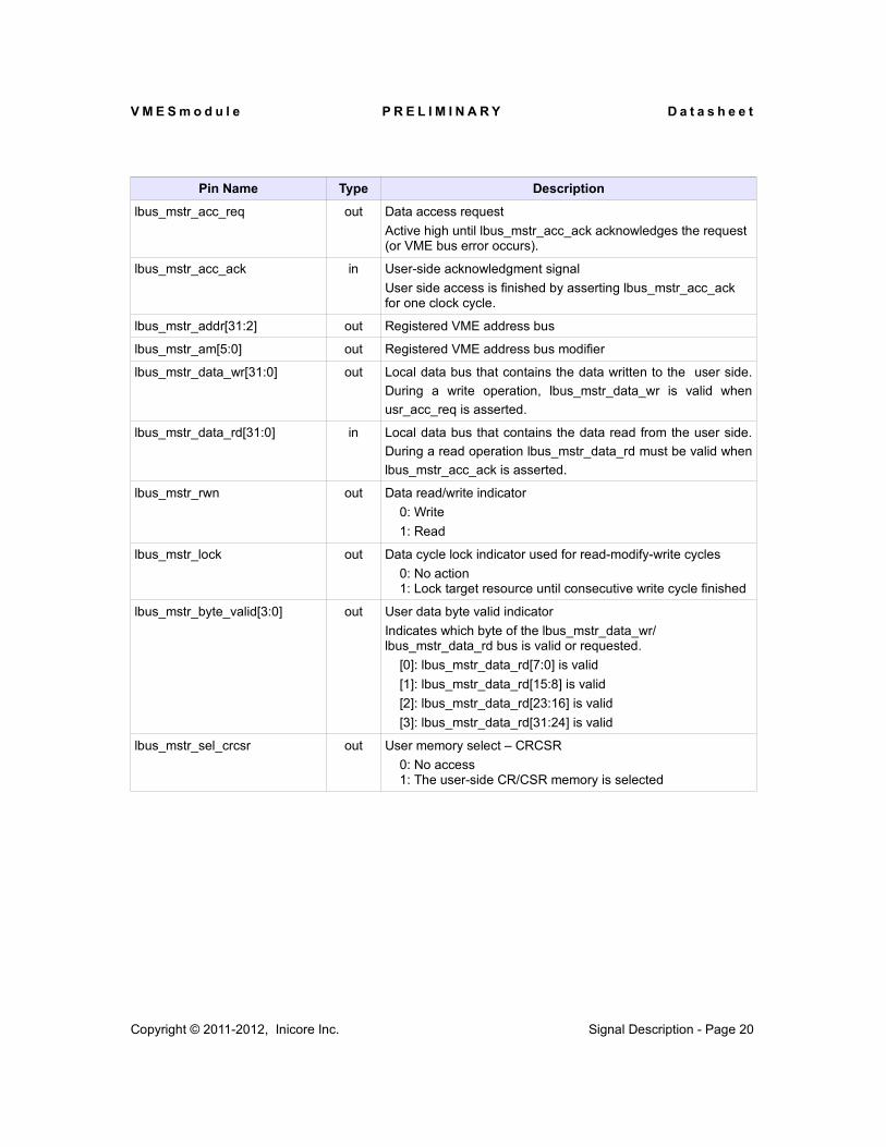
Pin Name Type Description
lbus_mstr_acc_req out Data access requestActive high until lbus_mstr_acc_ack acknowledges the request (or VME bus error occurs).
lbus_mstr_acc_ack in User-side acknowledgment signalUser side access is finished by asserting lbus_mstr_acc_ack for one clock cycle.
lbus_mstr_addr[31:2] out Registered VME address bus
lbus_mstr_am[5:0] out Registered VME address bus modifier
lbus_mstr_data_wr[31:0] out Local data bus that contains the data written to the user side. During a write operation, lbus_mstr_data_wr is valid when usr_acc_req is asserted.
lbus_mstr_data_rd[31:0] in Local data bus that contains the data read from the user side. During a read operation lbus_mstr_data_rd must be valid when lbus_mstr_acc_ack is asserted.
lbus_mstr_rwn out Data read/write indicator0: Write1: Read
lbus_mstr_lock out Data cycle lock indicator used for read-modify-write cycles0: No action1: Lock target resource until consecutive write cycle finished
lbus_mstr_byte_valid[3:0] out User data byte valid indicatorIndicates which byte of the lbus_mstr_data_wr/ lbus_mstr_data_rd bus is valid or requested.
[0]: lbus_mstr_data_rd[7:0] is valid[1]: lbus_mstr_data_rd[15:8] is valid[2]: lbus_mstr_data_rd[23:16] is valid[3]: lbus_mstr_data_rd[31:24] is valid
lbus_mstr_sel_crcsr out User memory select – CRCSR0: No access1: The user-side CR/CSR memory is selected
Copyright © 2011-2012, Inicore Inc. Signal Description - Page 20
V M E S m o d u l e P R E L I M I N A R Y D a t a s h e e t
Pin Name Type Description
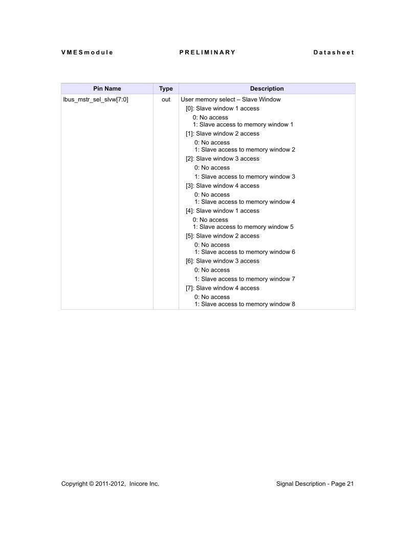
lbus_mstr_sel_slvw[7:0] out User memory select – Slave Window [0]: Slave window 1 access
0: No access 1: Slave access to memory window 1
[1]: Slave window 2 access 0: No access 1: Slave access to memory window 2
[2]: Slave window 3 access 0: No access 1: Slave access to memory window 3
[3]: Slave window 4 access 0: No access 1: Slave access to memory window 4
[4]: Slave window 1 access 0: No access 1: Slave access to memory window 5
[5]: Slave window 2 access 0: No access 1: Slave access to memory window 6
[6]: Slave window 3 access 0: No access 1: Slave access to memory window 7
[7]: Slave window 4 access 0: No access 1: Slave access to memory window 8
Copyright © 2011-2012, Inicore Inc. Signal Description - Page 21
V M E S m o d u l e P R E L I M I N A R Y D a t a s h e e t
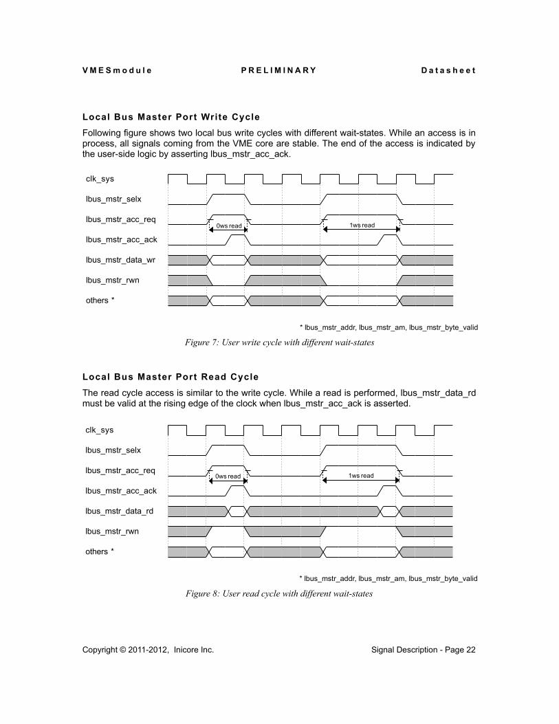
Local Bus Master Port Write Cycle
Following figure shows two local bus write cycles with different wait-states. While an access is in process, all signals coming from the VME core are stable. The end of the access is indicated by the user-side logic by asserting lbus_mstr_acc_ack.
Local Bus Master Port Read Cycle
The read cycle access is similar to the write cycle. While a read is performed, lbus_mstr_data_rd must be valid at the rising edge of the clock when lbus_mstr_acc_ack is asserted.
Copyright © 2011-2012, Inicore Inc. Signal Description - Page 22
* lbus_mstr_addr, lbus_mstr_am, lbus_mstr_byte_valid
Figure 8: User read cycle with different wait-states
* lbus_mstr_addr, lbus_mstr_am, lbus_mstr_byte_valid
Figure 7: User write cycle with different wait-states
1ws read0ws read
0ws read 1ws read
clk_sys
lbus_mstr_selx
lbus_mstr_acc_req
lbus_mstr_acc_ack
lbus_mstr_data_wr
lbus_mstr_rwn
others *
1ws read0ws read
0ws read 1ws read
clk_sys
lbus_mstr_selx
lbus_mstr_acc_req
lbus_mstr_acc_ack
lbus_mstr_data_rd
lbus_mstr_rwn
others *
V M E S m o d u l e P R E L I M I N A R Y D a t a s h e e t
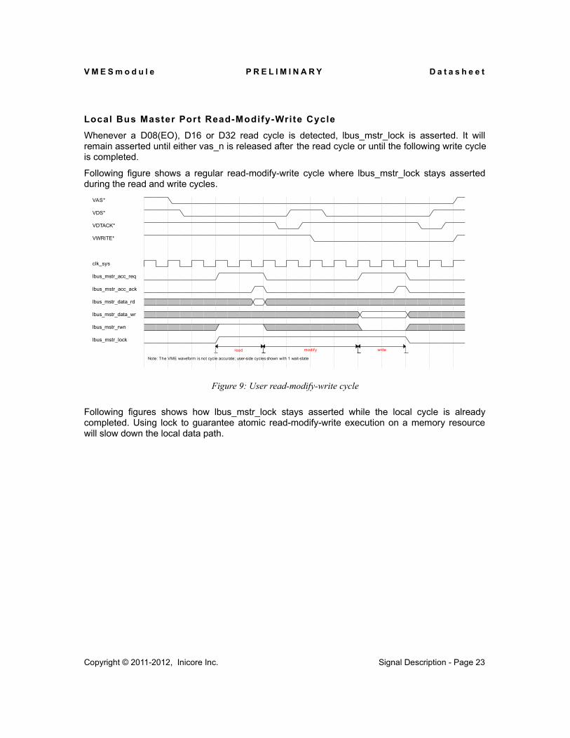
Local Bus Master Port Read-Modify-Write Cycle
Whenever a D08(EO), D16 or D32 read cycle is detected, lbus_mstr_lock is asserted. It will remain asserted until either vas_n is released after the read cycle or until the following write cycle is completed.
Following figure shows a regular read-modify-write cycle where lbus_mstr_lock stays asserted during the read and write cycles.
Following figures shows how lbus_mstr_lock stays asserted while the local cycle is already completed. Using lock to guarantee atomic read-modify-write execution on a memory resource will slow down the local data path.
Copyright © 2011-2012, Inicore Inc. Signal Description - Page 23
Figure 9: User read-modify-write cycle
read writemodify
Note: The VME waveform is not cycle accurate; user-side cycles shown with 1 wait-state
VAS*
VDS*
VDTACK*
VWRITE*
clk_sys
lbus_mstr_acc_req
lbus_mstr_acc_ack
lbus_mstr_data_rd
lbus_mstr_data_wr
lbus_mstr_rwn
lbus_mstr_lock
V M E S m o d u l e P R E L I M I N A R Y D a t a s h e e t
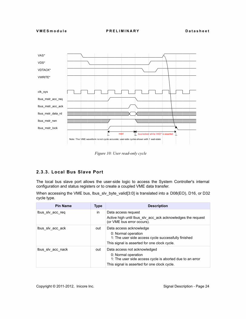
2.3.3. Local Bus Slave Port
The local bus slave port allows the user-side logic to access the System Controller's internal configuration and status registers or to create a coupled VME data transfer.
When accessing the VME bus, lbus_slv_byte_valid[3:0] is translated into a D08(EO), D16, or D32 cycle type.
Pin Name Type Description
lbus_slv_acc_req in Data access requestActive high until lbus_slv_acc_ack acknowledges the request (or VME bus error occurs).
lbus_slv_acc_ack out Data access acknowledge0: Normal operation1: The user side access cycle successfully finished
This signal is asserted for one clock cycle.
lbus_slv_acc_nack out Data access not acknowledged0: Normal operation1: The user side access cycle is aborted due to an error
This signal is asserted for one clock cycle.
Copyright © 2011-2012, Inicore Inc. Signal Description - Page 24
Figure 10: User read-only cycle
read bus locked while VAS* is asserted
Note: The VME waveform is not cycle accurate; user-side cycles shown with 1 wait-state
VAS*
VDS*
VDTACK*
VWRITE*
clk_sys
lbus_mstr_acc_req
lbus_mstr_acc_ack
lbus_mstr_data_rd
lbus_mstr_rwn
lbus_mstr_lock
V M E S m o d u l e P R E L I M I N A R Y D a t a s h e e t
Pin Name Type Description
lbus_slv_addr[9:2] in Access addressFor CR/CSR memory space access, only the bit range [9:2] is taken into account.
lbus_slv_data_wr[31:0] in Data write bus
lbus_slv_data_rd[31:0] out Data read bus
lbus_slv_byte_valid[3:0] in Data byte valid indicatorIndicates which byte of the lbus_slv_data_wr is valid.
[0]: lbus_slv_data_wr[7:0] is valid[1]: lbus_slv_data_wr[15:8] is valid[2]: lbus_slv_data_wr[23:16] is valid[3]: lbus_slv_data_wr[31:24] is valid
Note: A read operation always returns the 32-bit value independently of the lbus_slv_byte_valid settings.
lbus_slv_rwn in Data read/write indicator 0: Write1: Read
lbus_slv_lock in Data cycle lock indicator used for read-modify-write cycles0: No action1: Lock target resource until consecutive cycle finished
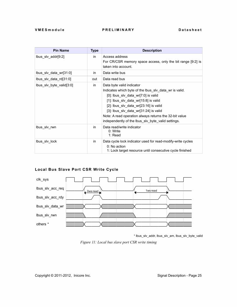
Local Bus Slave Port CSR Write Cycle
Copyright © 2011-2012, Inicore Inc. Signal Description - Page 25
* lbus_slv_addr, lbus_slv_am, lbus_slv_byte_valid
Figure 11: Local bus slave port CSR write timing
1ws read0ws read
0ws read 1ws read
clk_sys
lbus_slv_acc_req
lbus_slv_acc_rdy
lbus_slv_data_wr
lbus_slv_rwn
others *
V M E S m o d u l e P R E L I M I N A R Y D a t a s h e e t
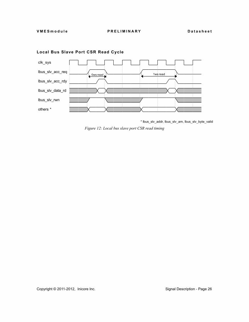
Local Bus Slave Port CSR Read Cycle
Copyright © 2011-2012, Inicore Inc. Signal Description - Page 26
* lbus_slv_addr, lbus_slv_am, lbus_slv_byte_valid
Figure 12: Local bus slave port CSR read timing
1ws read0ws read
0ws read 1ws read
clk_sys
lbus_slv_acc_req
lbus_slv_acc_rdy
lbus_slv_data_rd
lbus_slv_rwn
others *
V M E S m o d u l e P R E L I M I N A R Y D a t a s h e e t
3 . C or e C on f i g ur a t i o n
The core behavior can be set by using following top-level generics:
Generic Name Description
G_VME_SLVWx_AVx=1..8
Slave window availableFor gate-count optimization, each slave access window can individually disabled.
0: Slave window is not available1: Slave window is available
G_VME_SLVWx_SIZEx=1..8
Slave window sizeThe window size is defined as 256 x 2G_VME_SLVWx_SIZE :
0: 256 bytes1: 512 bytes2: 1k bytes…15: 8M bytesOthers: not valid
G_SYSFAIL_MODE SYSFAIL* Mode SelectionUpon hardware reset or a system reset, the core asserts SYSFAIL*
0: Do not assert SYSFAIL* upon reset1: Assert SYSFAIL* upon reset
Once the core has completed its internal failure analysis routine, SYSFAIL* has to be released by the application by using the BIT_CLEAR.SDES register.
G_VME_SLV_DTACK Rescinding DTACK enable The VME slave block can use rescinding dtack to accelerate data trans-mission.
0: Disabled 1: Enabled
3.1. Rescinding DTACK
The VME64 specification allows DTACK to be operated as a rescinding signal instead of an open-collector class signal. This results in an accelerated bus cycle. This feature can be selected by setting the top level generic G_VME_SLV_DTACK = 1.
Copyright © 2011-2012, Inicore Inc. Core Configuration - Page 27
V M E S m o d u l e P R E L I M I N A R Y D a t a s h e e t
4 . P r o gr am m e r s Gu i d e
4.1. Internal CSR Memory Space
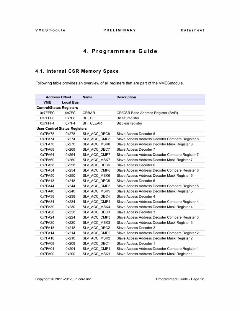
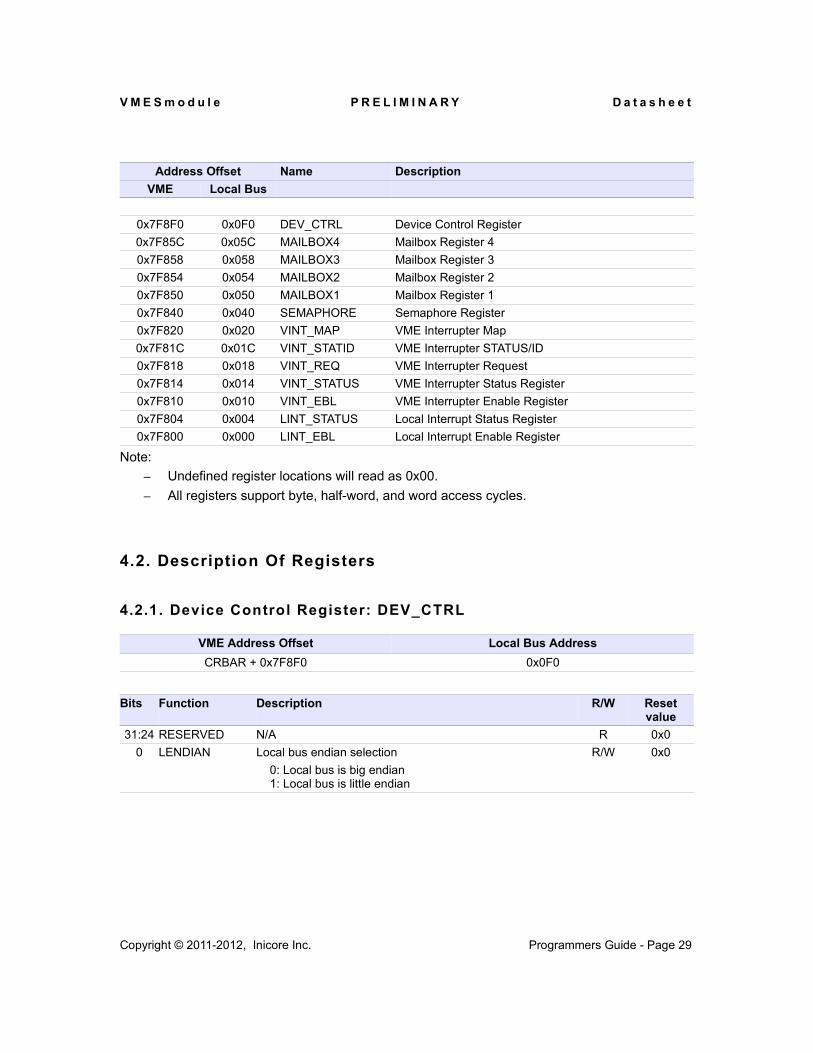
Following table provides an overview of all registers that are part of the VMESmodule.
Address Offset Name DescriptionVME Local Bus
Control/Status Registers0x7FFFC 0x7FC CRBAR CR/CSR Base Address Register (BAR)0x7FFF8 0x7F8 BIT_SET Bit set register0x7FFF4 0x7F4 BIT_CLEAR Bit clear register
User Control Status Registers0x7FA78 0x278 SLV_ACC_DEC8 Slave Access Decoder 80x7FA74 0x274 SLV_ACC_CMP8 Slave Access Address Decoder Compare Register 80x7FA70 0x270 SLV_ACC_MSK8 Slave Access Address Decoder Mask Register 80x7FA68 0x268 SLV_ACC_DEC7 Slave Access Decoder 70x7FA64 0x264 SLV_ACC_CMP7 Slave Access Address Decoder Compare Register 70x7FA60 0x260 SLV_ACC_MSK7 Slave Access Address Decoder Mask Register 70x7FA58 0x258 SLV_ACC_DEC6 Slave Access Decoder 60x7FA54 0x254 SLV_ACC_CMP6 Slave Access Address Decoder Compare Register 60x7FA50 0x250 SLV_ACC_MSK6 Slave Access Address Decoder Mask Register 60x7FA48 0x248 SLV_ACC_DEC5 Slave Access Decoder 50x7FA44 0x244 SLV_ACC_CMP5 Slave Access Address Decoder Compare Register 50x7FA40 0x240 SLV_ACC_MSK5 Slave Access Address Decoder Mask Register 50x7FA38 0x238 SLV_ACC_DEC4 Slave Access Decoder 40x7FA34 0x234 SLV_ACC_CMP4 Slave Access Address Decoder Compare Register 40x7FA30 0x230 SLV_ACC_MSK4 Slave Access Address Decoder Mask Register 40x7FA28 0x228 SLV_ACC_DEC3 Slave Access Decoder 30x7FA24 0x224 SLV_ACC_CMP3 Slave Access Address Decoder Compare Register 30x7FA20 0x220 SLV_ACC_MSK3 Slave Access Address Decoder Mask Register 30x7FA18 0x218 SLV_ACC_DEC2 Slave Access Decoder 20x7FA14 0x214 SLV_ACC_CMP2 Slave Access Address Decoder Compare Register 20x7FA10 0x210 SLV_ACC_MSK2 Slave Access Address Decoder Mask Register 20x7FA08 0x208 SLV_ACC_DEC1 Slave Access Decoder 10x7FA04 0x204 SLV_ACC_CMP1 Slave Access Address Decoder Compare Register 10x7FA00 0x200 SLV_ACC_MSK1 Slave Access Address Decoder Mask Register 1
Copyright © 2011-2012, Inicore Inc. Programmers Guide - Page 28
V M E S m o d u l e P R E L I M I N A R Y D a t a s h e e t
Address Offset Name DescriptionVME Local Bus
0x7F8F0 0x0F0 DEV_CTRL Device Control Register0x7F85C 0x05C MAILBOX4 Mailbox Register 40x7F858 0x058 MAILBOX3 Mailbox Register 30x7F854 0x054 MAILBOX2 Mailbox Register 20x7F850 0x050 MAILBOX1 Mailbox Register 10x7F840 0x040 SEMAPHORE Semaphore Register0x7F820 0x020 VINT_MAP VME Interrupter Map0x7F81C 0x01C VINT_STATID VME Interrupter STATUS/ID0x7F818 0x018 VINT_REQ VME Interrupter Request0x7F814 0x014 VINT_STATUS VME Interrupter Status Register0x7F810 0x010 VINT_EBL VME Interrupter Enable Register0x7F804 0x004 LINT_STATUS Local Interrupt Status Register0x7F800 0x000 LINT_EBL Local Interrupt Enable Register
Note:– Undefined register locations will read as 0x00.– All registers support byte, half-word, and word access cycles.
4.2. Description Of Registers
4.2.1. Device Control Register: DEV_CTRL
VME Address Offset Local Bus AddressCRBAR + 0x7F8F0 0x0F0
Bits Function Description R/W Resetvalue
31:24 RESERVED N/A R 0x00 LENDIAN Local bus endian selection
0: Local bus is big endian1: Local bus is little endian
R/W 0x0
Copyright © 2011-2012, Inicore Inc. Programmers Guide - Page 29
V M E S m o d u l e P R E L I M I N A R Y D a t a s h e e t
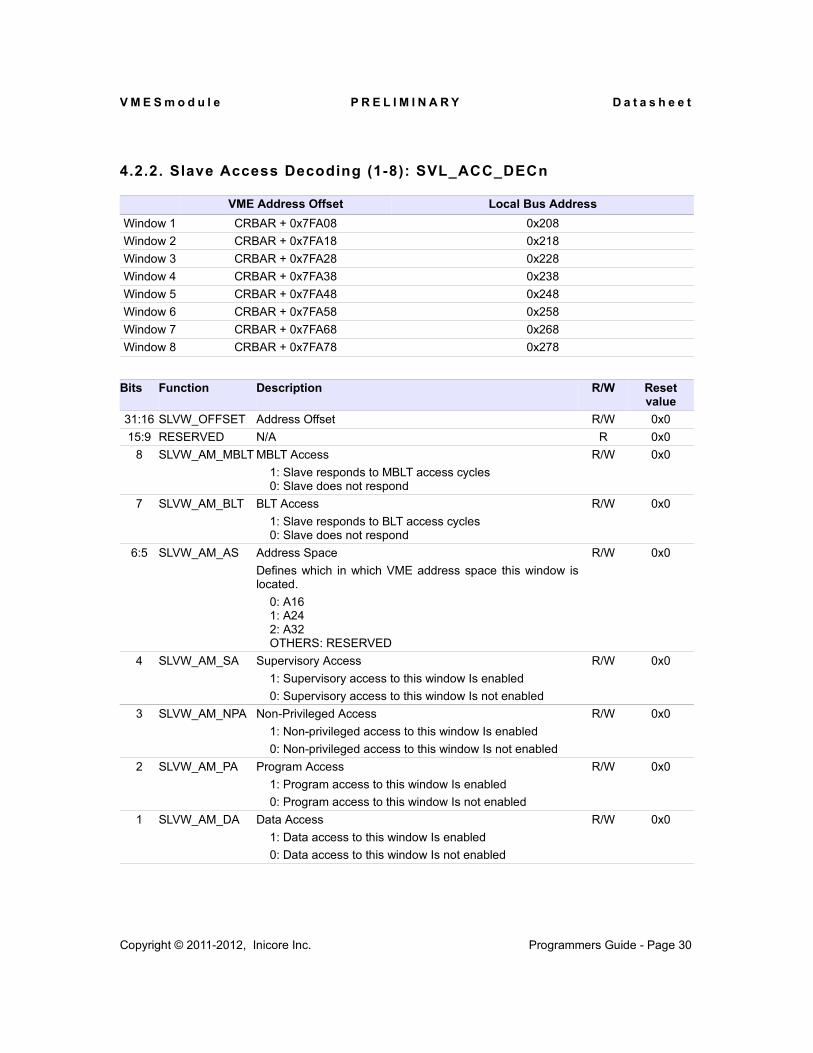
4.2.2. Slave Access Decoding (1-8): SVL_ACC_DECn
VME Address Offset Local Bus AddressWindow 1 CRBAR + 0x7FA08 0x208Window 2 CRBAR + 0x7FA18 0x218Window 3 CRBAR + 0x7FA28 0x228Window 4 CRBAR + 0x7FA38 0x238Window 5 CRBAR + 0x7FA48 0x248Window 6 CRBAR + 0x7FA58 0x258Window 7 CRBAR + 0x7FA68 0x268Window 8 CRBAR + 0x7FA78 0x278
Bits Function Description R/W Resetvalue
31:16 SLVW_OFFSET Address Offset R/W 0x015:9 RESERVED N/A R 0x0
8 SLVW_AM_MBLT MBLT Access1: Slave responds to MBLT access cycles0: Slave does not respond
R/W 0x0
7 SLVW_AM_BLT BLT Access1: Slave responds to BLT access cycles0: Slave does not respond
R/W 0x0
6:5 SLVW_AM_AS Address SpaceDefines which in which VME address space this window is located.
0: A161: A242: A32OTHERS: RESERVED
R/W 0x0
4 SLVW_AM_SA Supervisory Access1: Supervisory access to this window Is enabled0: Supervisory access to this window Is not enabled
R/W 0x0
3 SLVW_AM_NPA Non-Privileged Access1: Non-privileged access to this window Is enabled0: Non-privileged access to this window Is not enabled
R/W 0x0
2 SLVW_AM_PA Program Access1: Program access to this window Is enabled0: Program access to this window Is not enabled
R/W 0x0
1 SLVW_AM_DA Data Access1: Data access to this window Is enabled0: Data access to this window Is not enabled
R/W 0x0
Copyright © 2011-2012, Inicore Inc. Programmers Guide - Page 30
V M E S m o d u l e P R E L I M I N A R Y D a t a s h e e t
Bits Function Description R/W Resetvalue
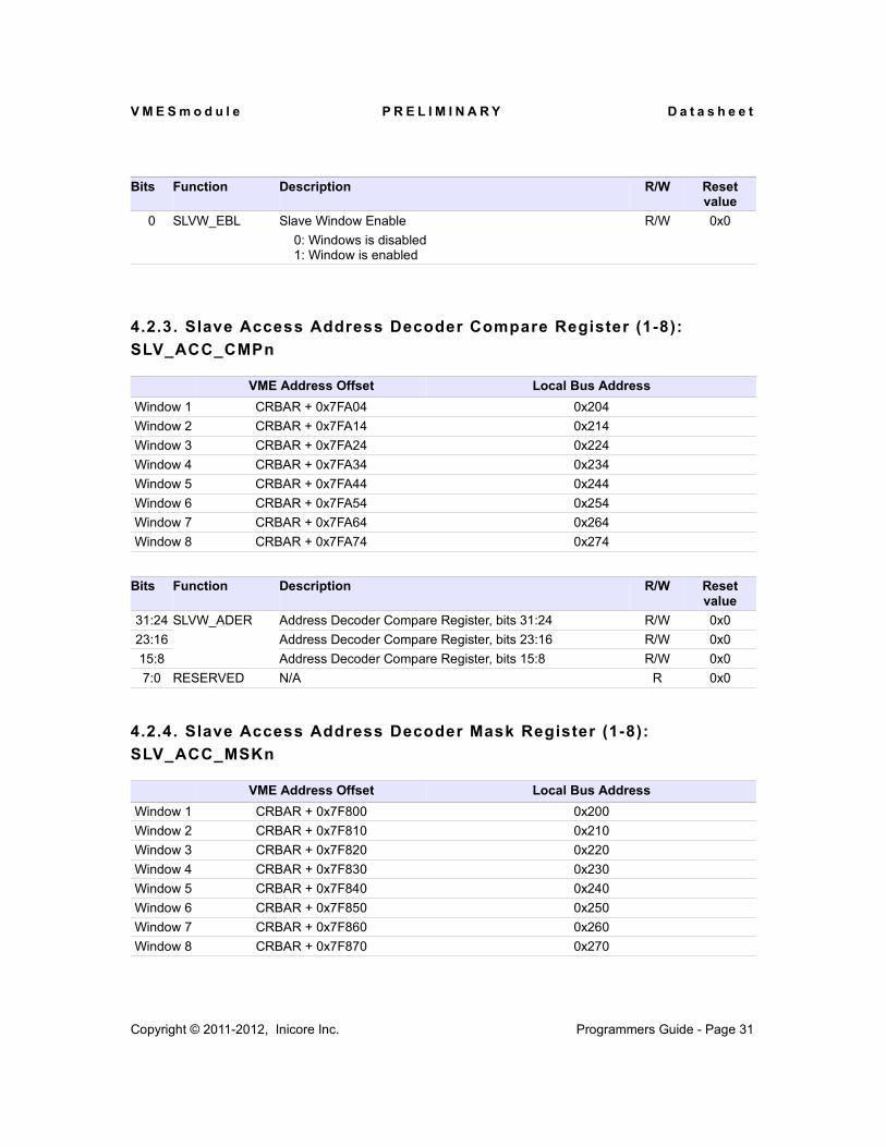
0 SLVW_EBL Slave Window Enable0: Windows is disabled1: Window is enabled
R/W 0x0
4.2.3. Slave Access Address Decoder Compare Register (1-8): SLV_ACC_CMPn
VME Address Offset Local Bus AddressWindow 1 CRBAR + 0x7FA04 0x204Window 2 CRBAR + 0x7FA14 0x214Window 3 CRBAR + 0x7FA24 0x224Window 4 CRBAR + 0x7FA34 0x234Window 5 CRBAR + 0x7FA44 0x244Window 6 CRBAR + 0x7FA54 0x254Window 7 CRBAR + 0x7FA64 0x264Window 8 CRBAR + 0x7FA74 0x274
Bits Function Description R/W Resetvalue
31:2423:1615:8
SLVW_ADER Address Decoder Compare Register, bits 31:24 R/W 0x0Address Decoder Compare Register, bits 23:16 R/W 0x0Address Decoder Compare Register, bits 15:8 R/W 0x0
7:0 RESERVED N/A R 0x0
4.2.4. Slave Access Address Decoder Mask Register (1-8): SLV_ACC_MSKn
VME Address Offset Local Bus AddressWindow 1 CRBAR + 0x7F800 0x200Window 2 CRBAR + 0x7F810 0x210Window 3 CRBAR + 0x7F820 0x220Window 4 CRBAR + 0x7F830 0x230Window 5 CRBAR + 0x7F840 0x240Window 6 CRBAR + 0x7F850 0x250Window 7 CRBAR + 0x7F860 0x260Window 8 CRBAR + 0x7F870 0x270
Copyright © 2011-2012, Inicore Inc. Programmers Guide - Page 31
V M E S m o d u l e P R E L I M I N A R Y D a t a s h e e t
Bits Function Description R/W Resetvalue
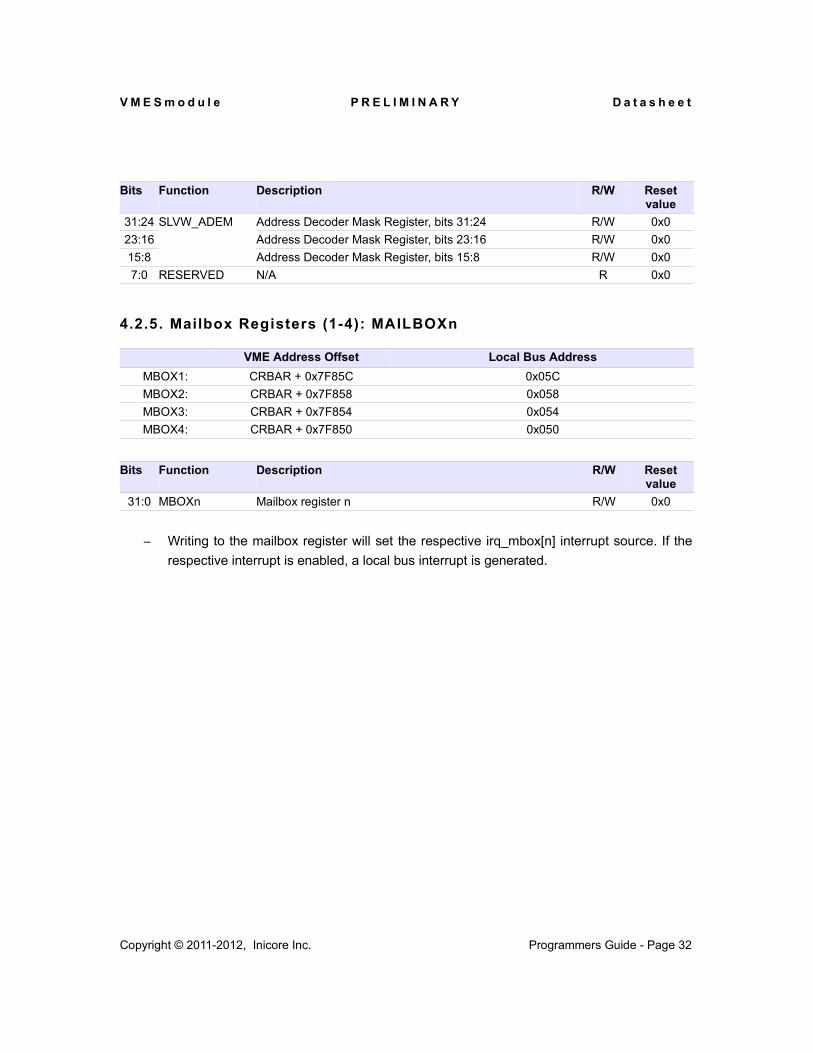
31:2423:1615:8
SLVW_ADEM Address Decoder Mask Register, bits 31:24 R/W 0x0Address Decoder Mask Register, bits 23:16 R/W 0x0Address Decoder Mask Register, bits 15:8 R/W 0x0
7:0 RESERVED N/A R 0x0
4.2.5. Mailbox Registers (1-4): MAILBOXn
VME Address Offset Local Bus AddressMBOX1: CRBAR + 0x7F85C 0x05CMBOX2: CRBAR + 0x7F858 0x058MBOX3: CRBAR + 0x7F854 0x054MBOX4: CRBAR + 0x7F850 0x050
Bits Function Description R/W Resetvalue
31:0 MBOXn Mailbox register n R/W 0x0
– Writing to the mailbox register will set the respective irq_mbox[n] interrupt source. If the respective interrupt is enabled, a local bus interrupt is generated.
Copyright © 2011-2012, Inicore Inc. Programmers Guide - Page 32
V M E S m o d u l e P R E L I M I N A R Y D a t a s h e e t
4.2.6. Semaphore Registers (0-3): SEMAPHORE
VME Address Offset Local Bus AddressCRBAR + 0x7F840 0x040
Bits Function Description R/W Resetvalue
31:24 SEMA3 Semaphore register 3
[31]: Semaphore bit 3[30:24]: Semaphore tag 3
R/W 0x0
23:16 SEMA2 Semaphore register 2
[23]: Semaphore bit 2[22:16]: Semaphore tag 2
R/W 0x0
15:8 SEMA1 Semaphore register 1
[15]: Semaphore bit 1[14:8]: Semaphore tag 1
R/W 0x0
7:0 SEMA0 Semaphore register 0
[7]: Semaphore bit 0[6:0]: Semaphore tag 0
R/W 0x0
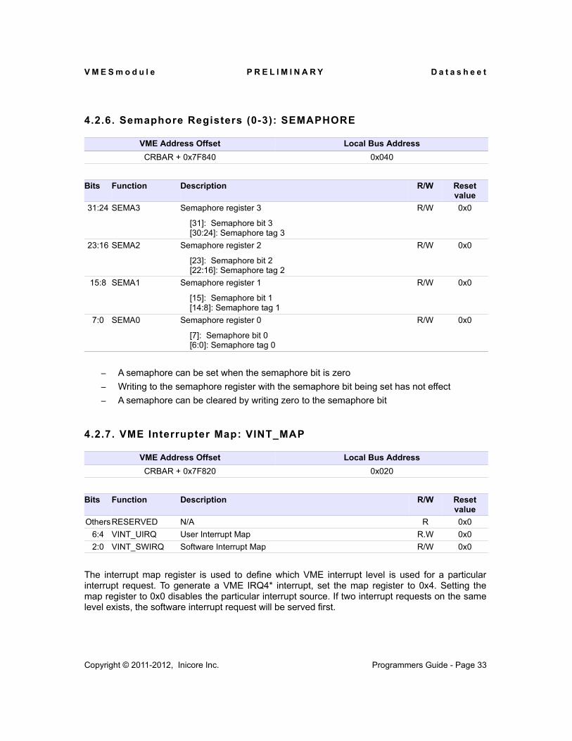
– A semaphore can be set when the semaphore bit is zero– Writing to the semaphore register with the semaphore bit being set has not effect– A semaphore can be cleared by writing zero to the semaphore bit
4.2.7. VME Interrupter Map: VINT_MAP
VME Address Offset Local Bus AddressCRBAR + 0x7F820 0x020
Bits Function Description R/W Resetvalue
OthersRESERVED N/A R 0x06:4 VINT_UIRQ User Interrupt Map R.W 0x02:0 VINT_SWIRQ Software Interrupt Map R/W 0x0
The interrupt map register is used to define which VME interrupt level is used for a particular interrupt request. To generate a VME IRQ4* interrupt, set the map register to 0x4. Setting the map register to 0x0 disables the particular interrupt source. If two interrupt requests on the same level exists, the software interrupt request will be served first.
Copyright © 2011-2012, Inicore Inc. Programmers Guide - Page 33
V M E S m o d u l e P R E L I M I N A R Y D a t a s h e e t
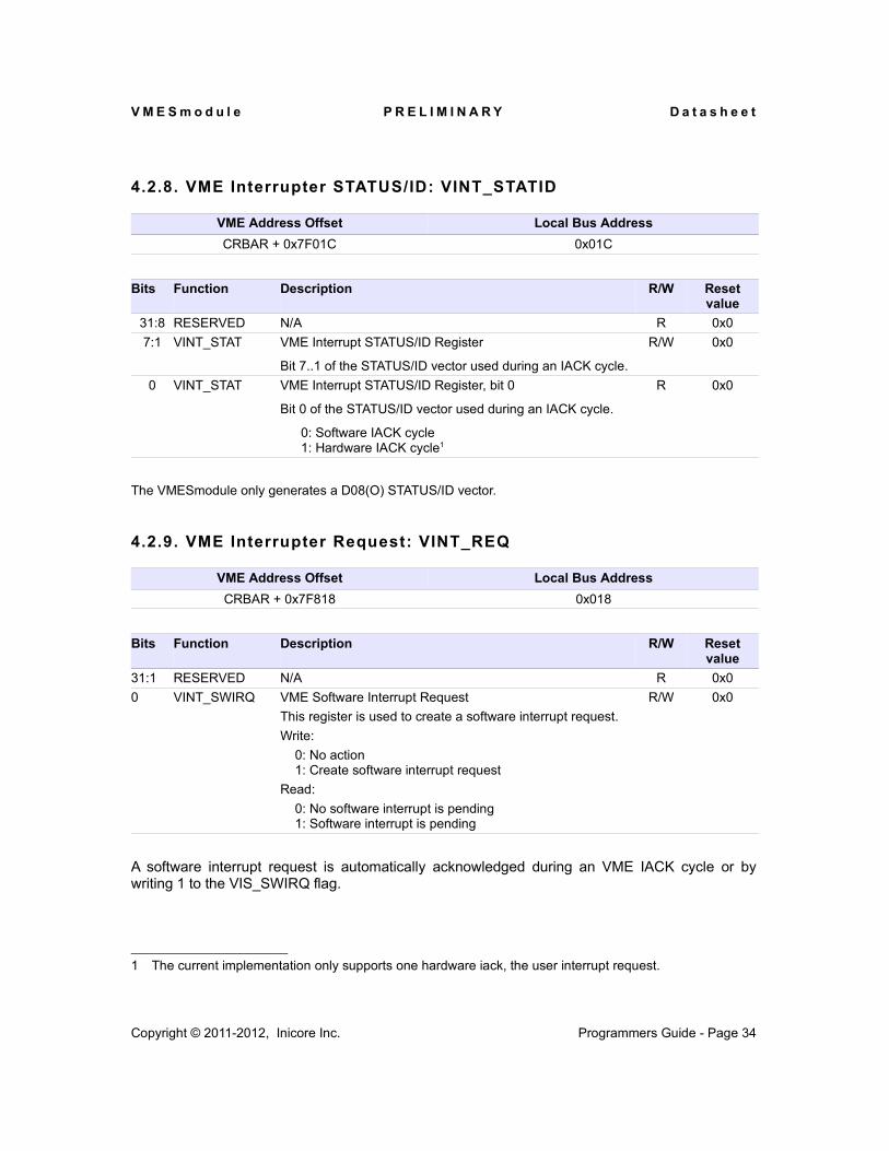
4.2.8. VME Interrupter STATUS/ID: VINT_STATID
VME Address Offset Local Bus AddressCRBAR + 0x7F01C 0x01C
Bits Function Description R/W Resetvalue
31:8 RESERVED N/A R 0x07:1 VINT_STAT VME Interrupt STATUS/ID Register
Bit 7..1 of the STATUS/ID vector used during an IACK cycle.
R/W 0x0
0 VINT_STAT VME Interrupt STATUS/ID Register, bit 0
Bit 0 of the STATUS/ID vector used during an IACK cycle.
0: Software IACK cycle1: Hardware IACK cycle1
R 0x0
The VMESmodule only generates a D08(O) STATUS/ID vector.
4.2.9. VME Interrupter Request: VINT_REQ
VME Address Offset Local Bus AddressCRBAR + 0x7F818 0x018
Bits Function Description R/W Resetvalue
31:1 RESERVED N/A R 0x00 VINT_SWIRQ VME Software Interrupt Request
This register is used to create a software interrupt request.Write:
0: No action1: Create software interrupt request
Read:0: No software interrupt is pending1: Software interrupt is pending
R/W 0x0
A software interrupt request is automatically acknowledged during an VME IACK cycle or by writing 1 to the VIS_SWIRQ flag.
1 The current implementation only supports one hardware iack, the user interrupt request.
Copyright © 2011-2012, Inicore Inc. Programmers Guide - Page 34
V M E S m o d u l e P R E L I M I N A R Y D a t a s h e e t
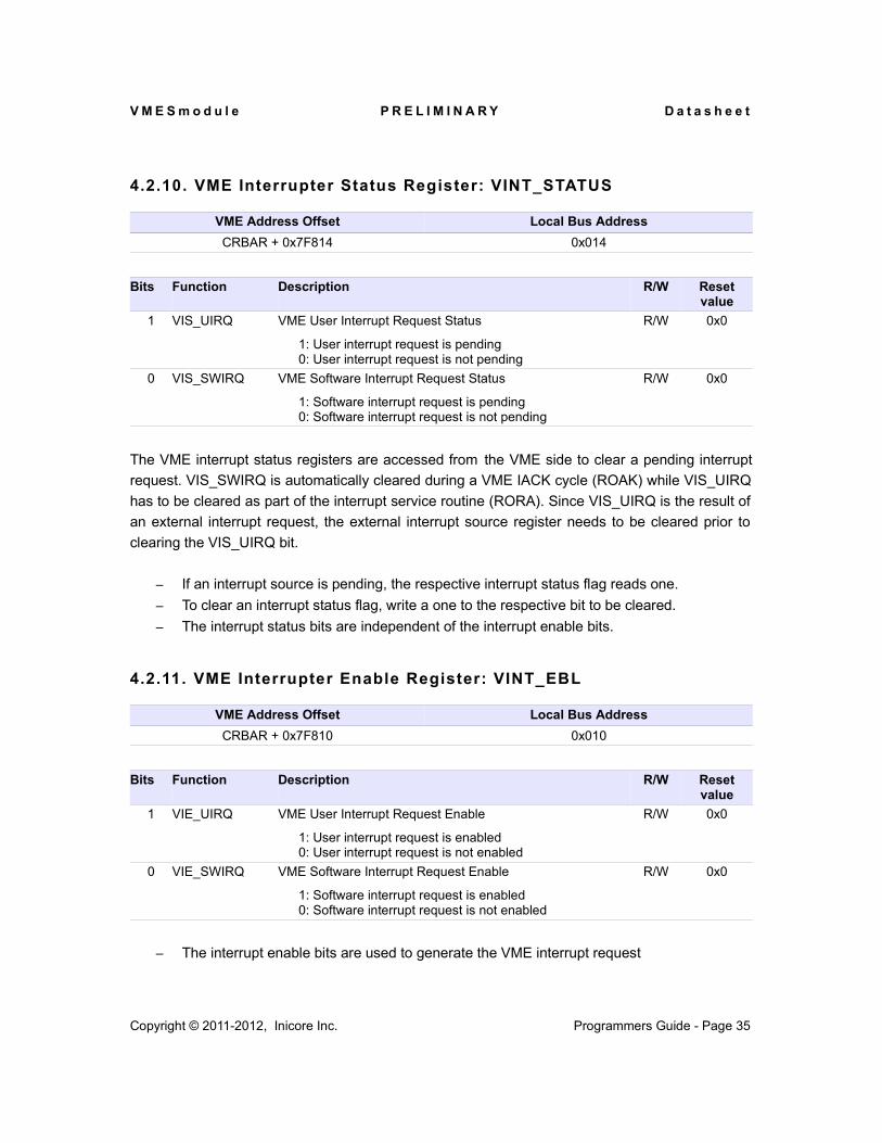
4.2.10. VME Interrupter Status Register: VINT_STATUS
VME Address Offset Local Bus AddressCRBAR + 0x7F814 0x014
Bits Function Description R/W Resetvalue
1 VIS_UIRQ VME User Interrupt Request Status
1: User interrupt request is pending0: User interrupt request is not pending
R/W 0x0
0 VIS_SWIRQ VME Software Interrupt Request Status
1: Software interrupt request is pending0: Software interrupt request is not pending
R/W 0x0
The VME interrupt status registers are accessed from the VME side to clear a pending interrupt request. VIS_SWIRQ is automatically cleared during a VME IACK cycle (ROAK) while VIS_UIRQ has to be cleared as part of the interrupt service routine (RORA). Since VIS_UIRQ is the result of an external interrupt request, the external interrupt source register needs to be cleared prior to clearing the VIS_UIRQ bit.
– If an interrupt source is pending, the respective interrupt status flag reads one.– To clear an interrupt status flag, write a one to the respective bit to be cleared.– The interrupt status bits are independent of the interrupt enable bits.
4.2.11. VME Interrupter Enable Register: VINT_EBL
VME Address Offset Local Bus AddressCRBAR + 0x7F810 0x010
Bits Function Description R/W Resetvalue
1 VIE_UIRQ VME User Interrupt Request Enable
1: User interrupt request is enabled0: User interrupt request is not enabled
R/W 0x0
0 VIE_SWIRQ VME Software Interrupt Request Enable
1: Software interrupt request is enabled0: Software interrupt request is not enabled
R/W 0x0
– The interrupt enable bits are used to generate the VME interrupt request
Copyright © 2011-2012, Inicore Inc. Programmers Guide - Page 35
V M E S m o d u l e P R E L I M I N A R Y D a t a s h e e t
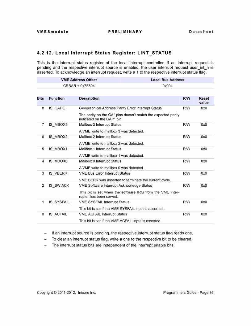
4.2.12. Local Interrupt Status Register: LINT_STATUS
This is the interrupt status register of the local interrupt controller. If an interrupt request is pending and the respective interrupt source is enabled, the user interrupt request user_int_n is asserted. To acknowledge an interrupt request, write a 1 to the respective interrupt status flag.
VME Address Offset Local Bus AddressCRBAR + 0x7F804 0x004
Bits Function Description R/W Resetvalue
8 IS_GAPE Geographical Address Parity Error Interrupt Status
The parity on the GA* pins doesn't match the expected parity indicated on the GAP* pin.
R/W 0x0
7 IS_MBOX3 Mailbox 3 Interrupt Status
A VME write to mailbox 3 was detected.
R/W 0x0
6 IS_MBOX2 Mailbox 2 Interrupt Status
A VME write to mailbox 2 was detected.
R/W 0x0
5 IS_MBOX1 Mailbox 1 Interrupt Status
A VME write to mailbox 1 was detected.
R/W 0x0
4 IS_MBOX0 Mailbox 0 Interrupt Status
A VME write to mailbox 0 was detected.
R/W 0x0
3 IS_VBERR VME Bus Error Interrupt Status
VME BERR was asserted to terminate the current cycle.
R/W 0x0
2 IS_SWIACK VME Software Interrupt Acknowledge Status
This bit is set when the software IRQ from the VME inter-rupter has been served.
R/W 0x0
1 IS_SYSFAIL VME SYSFAIL Interrupt Status
This bit is set if the VME SYSFAIL input is asserted.
R/W 0x0
0 IS_ACFAIL VME ACFAIL Interrupt Status
This bit is set if the VME ACFAIL input is asserted.
R/W 0x0
– If an interrupt source is pending, the respective interrupt status flag reads one.– To clear an interrupt status flag, write a one to the respective bit to be cleared.– The interrupt status bits are independent of the interrupt enable bits.
Copyright © 2011-2012, Inicore Inc. Programmers Guide - Page 36
V M E S m o d u l e P R E L I M I N A R Y D a t a s h e e t
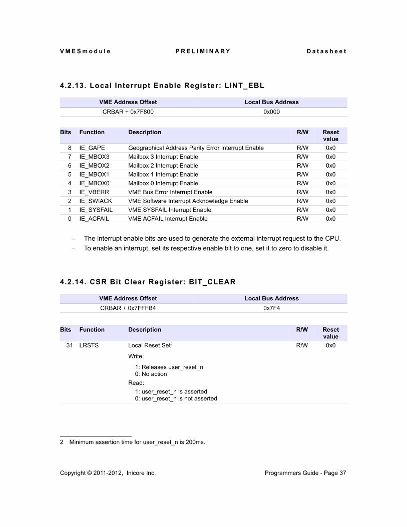
4.2.13. Local Interrupt Enable Register: LINT_EBL
VME Address Offset Local Bus AddressCRBAR + 0x7F800 0x000
Bits Function Description R/W Resetvalue
8 IE_GAPE Geographical Address Parity Error Interrupt Enable R/W 0x07 IE_MBOX3 Mailbox 3 Interrupt Enable R/W 0x06 IE_MBOX2 Mailbox 2 Interrupt Enable R/W 0x05 IE_MBOX1 Mailbox 1 Interrupt Enable R/W 0x04 IE_MBOX0 Mailbox 0 Interrupt Enable R/W 0x03 IE_VBERR VME Bus Error Interrupt Enable R/W 0x02 IE_SWIACK VME Software Interrupt Acknowledge Enable R/W 0x01 IE_SYSFAIL VME SYSFAIL Interrupt Enable R/W 0x00 IE_ACFAIL VME ACFAIL Interrupt Enable R/W 0x0
– The interrupt enable bits are used to generate the external interrupt request to the CPU.– To enable an interrupt, set its respective enable bit to one, set it to zero to disable it.
4.2.14. CSR Bit Clear Register: BIT_CLEAR
VME Address Offset Local Bus AddressCRBAR + 0x7FFFB4 0x7F4
Bits Function Description R/W Resetvalue
31 LRSTS Local Reset Set2
Write:
1: Releases user_reset_n0: No action
Read:1: user_reset_n is asserted0: user_reset_n is not asserted
R/W 0x0
2 Minimum assertion time for user_reset_n is 200ms.
Copyright © 2011-2012, Inicore Inc. Programmers Guide - Page 37
V M E S m o d u l e P R E L I M I N A R Y D a t a s h e e t
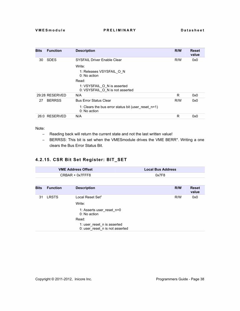
Bits Function Description R/W Resetvalue
30 SDES SYSFAIL Driver Enable Clear
Write:1: Releases VSYSFAIL_O_N0: No action
Read:1: VSYSFAIL_O_N is asserted0: VSYSFAIL_O_N is not asserted
R/W 0x0
29:28 RESERVED N/A R 0x027 BERRSS Bus Error Status Clear
1: Clears the bus error status bit (user_reset_n=1)0: No action
R/W 0x0
26:0 RESERVED N/A R 0x0
Note:– Reading back will return the current state and not the last written value!– BERRSS: This bit is set when the VMESmodule drives the VME BERR*. Writing a one
clears the Bus Error Status Bit.
4.2.15. CSR Bit Set Register: BIT_SET
VME Address Offset Local Bus AddressCRBAR + 0x7FFF8 0x7F8
Bits Function Description R/W Resetvalue
31 LRSTS Local Reset Set2
Write:
1: Asserts user_reset_n=00: No action
Read:1: user_reset_n is asserted0: user_reset_n is not asserted
R/W 0x0
Copyright © 2011-2012, Inicore Inc. Programmers Guide - Page 38
V M E S m o d u l e P R E L I M I N A R Y D a t a s h e e t
Bits Function Description R/W Resetvalue
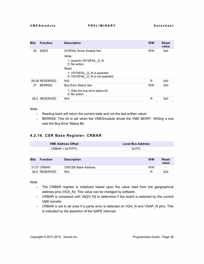
30 SDES SYSFAIL Driver Enable Set
Write:1: Asserts VSYSFAIL_O_N0: No action
Read:1: VSYSFAIL_O_N is asserted0: VSYSFAIL_O_N is not asserted
R/W 0x0
29:28 RESERVED N/A R 0x027 BERRSS Bus Error Status Set
1: Sets the bus error status bit0: No action
R/W 0x0
26:0 RESERVED N/A R 0x0
Note:– Reading back will return the current state and not the last written value!– BERRSS: This bit is set when the VMESmodule drives the VME BERR*. Writing a one
sets the Bus Error Status Bit.
4.2.16. CSR Base Register: CRBAR
VME Address Offset Local Bus AddressCRBAR + 0x7FFFC 0x7FC
Bits Function Description R/W Resetvalue
31:27 CRBAR CR/CSR Base Address R/W -26:0 RESERVED N/A R 0x0
Note:– The CRBAR register is initialized based upon the value read from the geographical
address pins (VGA_N). This value can be changed by software.– CRBAR is compared with VA[23:19] to determine if the board is selected by the current
VME transfer.– CRBAR is set to all ones if a parity error is detected on VGA_N and VGAP_N pins. This
is indicated by the assertion of the GAPE interrupt.
Copyright © 2011-2012, Inicore Inc. Programmers Guide - Page 39

V M E S m o d u l e P R E L I M I N A R Y D a t a s h e e t
Ab ou t In i c or e
FPGA and ASIC Design
Easy-to-use IP Cores
System-on-Chip Solutions
Consulting Services
ASIC to FPGA Migration
Obsolete ASIC Replacements
Inicore is an experienced system design house providing FPGA / ASIC and SoC design services. The company's expertise in architecture, intellectual property, methodology and tool handling provides a complete design environment that helps customers shorten their design cycle and speed time to market. Our offering covers feasibility study, concept analysis, architecture defini -tion, code generation and implementation. When ready, we deliver you a FPGA or take your design to an ASIC provider, whatever is more suitable for your unique solution.
Customer Advantages
We offer one-stop shopping for everything from the specifications to the chip or module solution. Our experience and fast turnaround time reduces your development costs and increases your returns from the market. Your system is not limited by the level of expertise and standard chip solutions you happen to have in-house. Achieve market success by differentiating and optimizing your product. Reusability builds the basis for further developments in the ever-decreasing product life cycle.
Visit us @ www.inicore.com
INICORE INC. has made every attempt to ensure that the information in this document is accurate and complete. However, INICORE INC. assumes no responsibility for any errors, omissions, or for any consequences resulting from the information included in this document or the equipments it accompanies. INICORE INC. reserves the right to make changes in its products and specifications at any time without notice.
Copyright © 2011-2012, INICORE INC. All rights reserved.
Copyright © 2011-2012, Inicore Inc. Programmers Guide - Page 40