helixeon hmep-c1pm hmep-c1pnsabalight.com/wp-content/uploads/2017/09/helixeon_ir_ehmep-c1pmn.pdf ·...
TRANSCRIPT
Doc. No.:DS-35-11-02
HELIO Optoelectronics Corp.
The information contained herein is the exclusive property of HELIO and shall not be distributed reproduced, or
disclosed in whole or in part without prior written permission of HELIO.
1
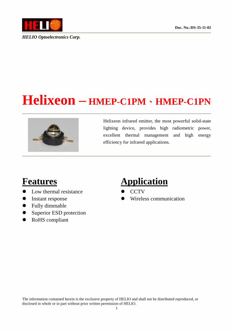
Helixeon – HMEP-C1PM、HMEP-C1PN
Helixeon infrared emitter, the most powerful solid-state
lighting device, provides high radiometric power,
excellent thermal management and high energy
efficiency for infrared applications.
Features Low thermal resistance
Instant response
Fully dimmable
Superior ESD protection
RoHS compliant
Application CCTV
Wireless communication
Doc. No.:DS-35-11-02
HELIO Optoelectronics Corp.
The information contained herein is the exclusive property of HELIO and shall not be distributed reproduced, or
disclosed in whole or in part without prior written permission of HELIO.
2
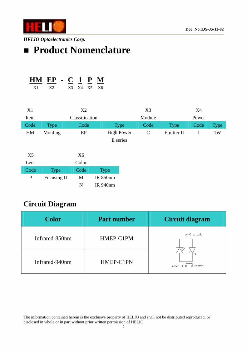
Product Nomenclature
HM EP - C 1 P M X1 X2 X3 X4 X5 X6
X1 X2 X3 X4
Item Classification Module Power
Code Type Code Type Code Type Code Type
HM Molding EP High Power C Emitter II 1 1W
E series
X5 X6
Lens Color
Code Type Code Type
P Focusing II M IR 850nm
N IR 940nm
Circuit Diagram
Color Part number Circuit diagram
Infrared-850nm HMEP-C1PM
Infrared-940nm HMEP-C1PN
Doc. No.:DS-35-11-02
HELIO Optoelectronics Corp.
The information contained herein is the exclusive property of HELIO and shall not be distributed reproduced, or
disclosed in whole or in part without prior written permission of HELIO.
3
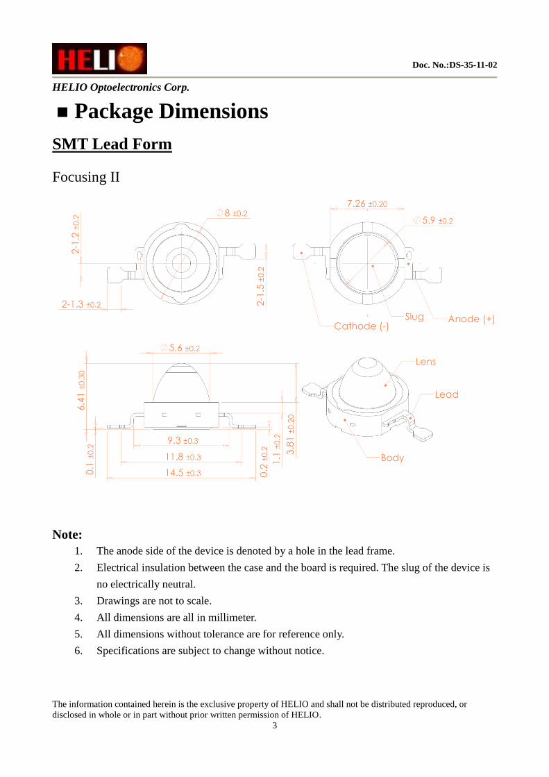
Package Dimensions
SMT Lead Form
Focusing II
Note:
1. The anode side of the device is denoted by a hole in the lead frame.
2. Electrical insulation between the case and the board is required. The slug of the device is
no electrically neutral.
3. Drawings are not to scale.
4. All dimensions are all in millimeter.
5. All dimensions without tolerance are for reference only.
6. Specifications are subject to change without notice.
Doc. No.:DS-35-11-02
HELIO Optoelectronics Corp.
The information contained herein is the exclusive property of HELIO and shall not be distributed reproduced, or
disclosed in whole or in part without prior written permission of HELIO.
4
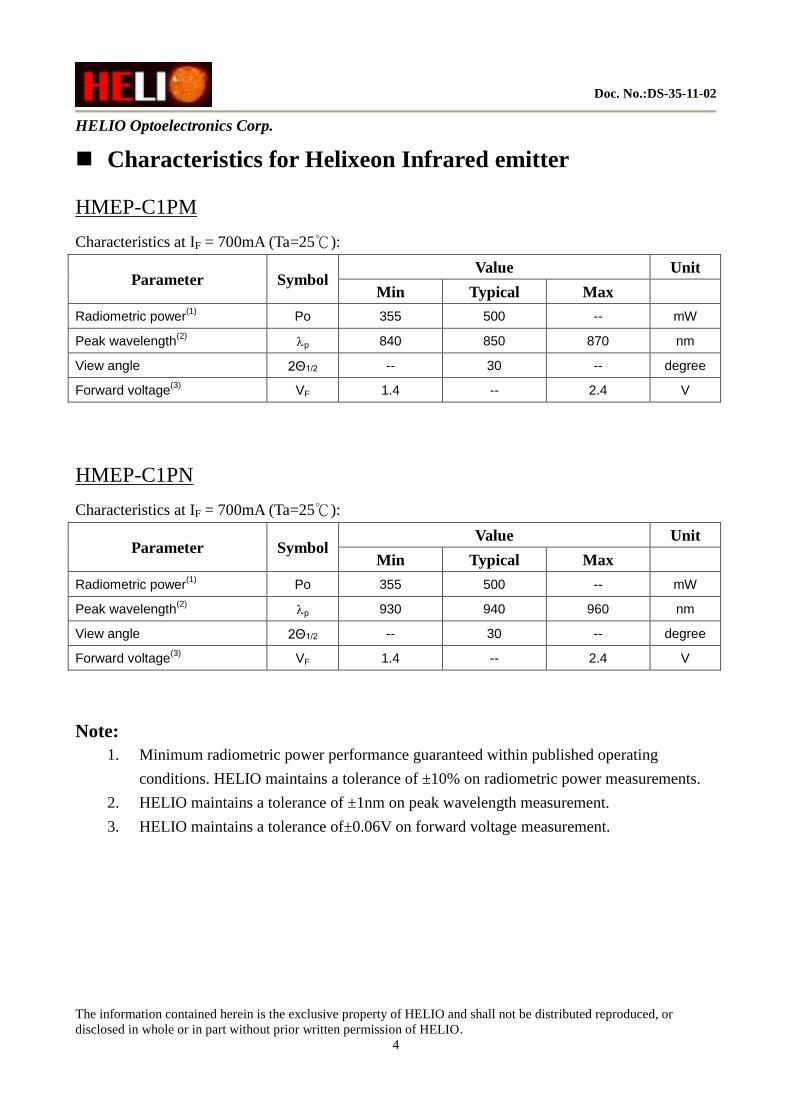
Characteristics for Helixeon Infrared emitter
HMEP-C1PM
Characteristics at IF = 700mA (Ta=25℃):
Parameter Symbol Value Unit
Min Typical Max
Radiometric power(1)
Po
355 500 -- mW
Peak wavelength(2)
p 840 850 870 nm
View angle 2Θ1/2 -- 30 -- degree
Forward voltage(3)
VF 1.4 -- 2.4 V
HMEP-C1PN
Characteristics at IF = 700mA (Ta=25℃):
Parameter Symbol Value Unit
Min Typical Max
Radiometric power(1)
Po
355 500 -- mW
Peak wavelength(2)
p 930 940 960 nm
View angle 2Θ1/2 -- 30 -- degree
Forward voltage(3)
VF 1.4 -- 2.4 V
Note:
1. Minimum radiometric power performance guaranteed within published operating
conditions. HELIO maintains a tolerance of ±10% on radiometric power measurements.
2. HELIO maintains a tolerance of ±1nm on peak wavelength measurement.
3. HELIO maintains a tolerance of±0.06V on forward voltage measurement.
Doc. No.:DS-35-11-02
HELIO Optoelectronics Corp.
The information contained herein is the exclusive property of HELIO and shall not be distributed reproduced, or
disclosed in whole or in part without prior written permission of HELIO.
5
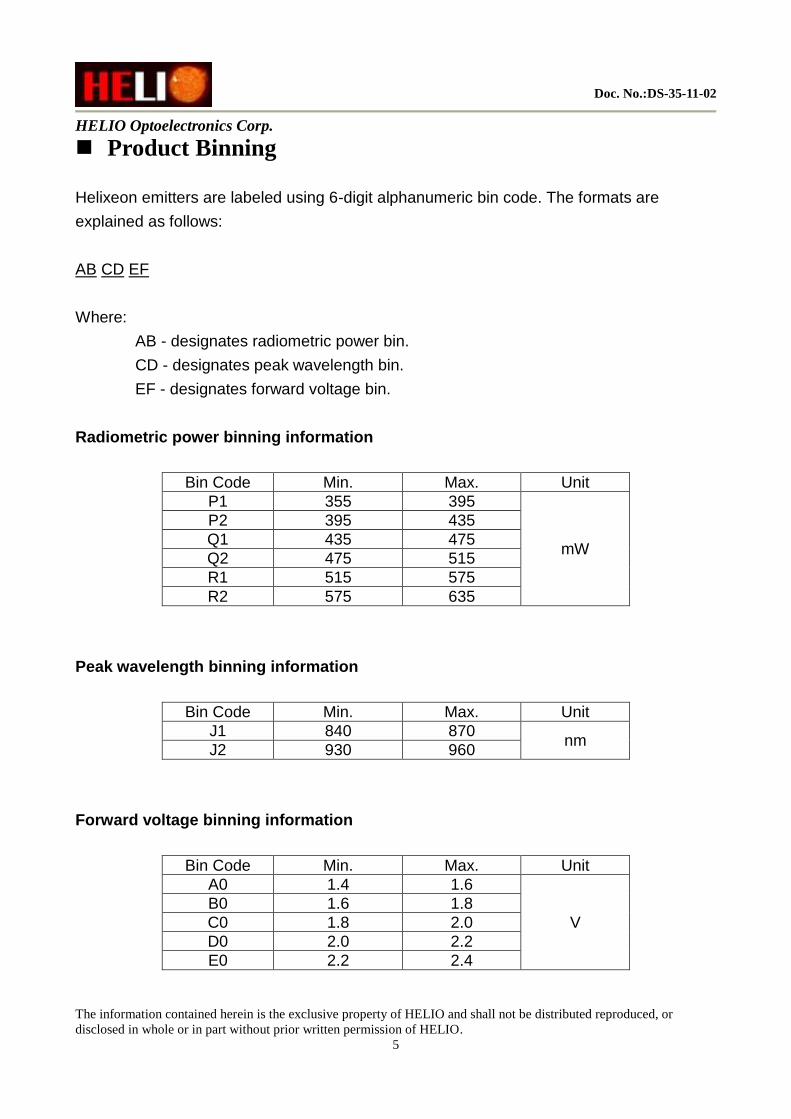
Product Binning
Helixeon emitters are labeled using 6-digit alphanumeric bin code. The formats are
explained as follows:
AB CD EF
Where:
AB - designates radiometric power bin.
CD - designates peak wavelength bin.
EF - designates forward voltage bin.
Radiometric power binning information
Bin Code Min. Max. Unit
P1 355 395
mW
P2 395 435
Q1 435 475
Q2 475 515
R1 515 575
R2 575 635
Peak wavelength binning information
Bin Code Min. Max. Unit
J1 840 870 nm
J2 930 960
Forward voltage binning information
Bin Code Min. Max. Unit
A0 1.4 1.6
V
B0 1.6 1.8
C0 1.8 2.0
D0 2.0 2.2
E0 2.2 2.4
Doc. No.:DS-35-11-02
HELIO Optoelectronics Corp.
The information contained herein is the exclusive property of HELIO and shall not be distributed reproduced, or
disclosed in whole or in part without prior written permission of HELIO.
6
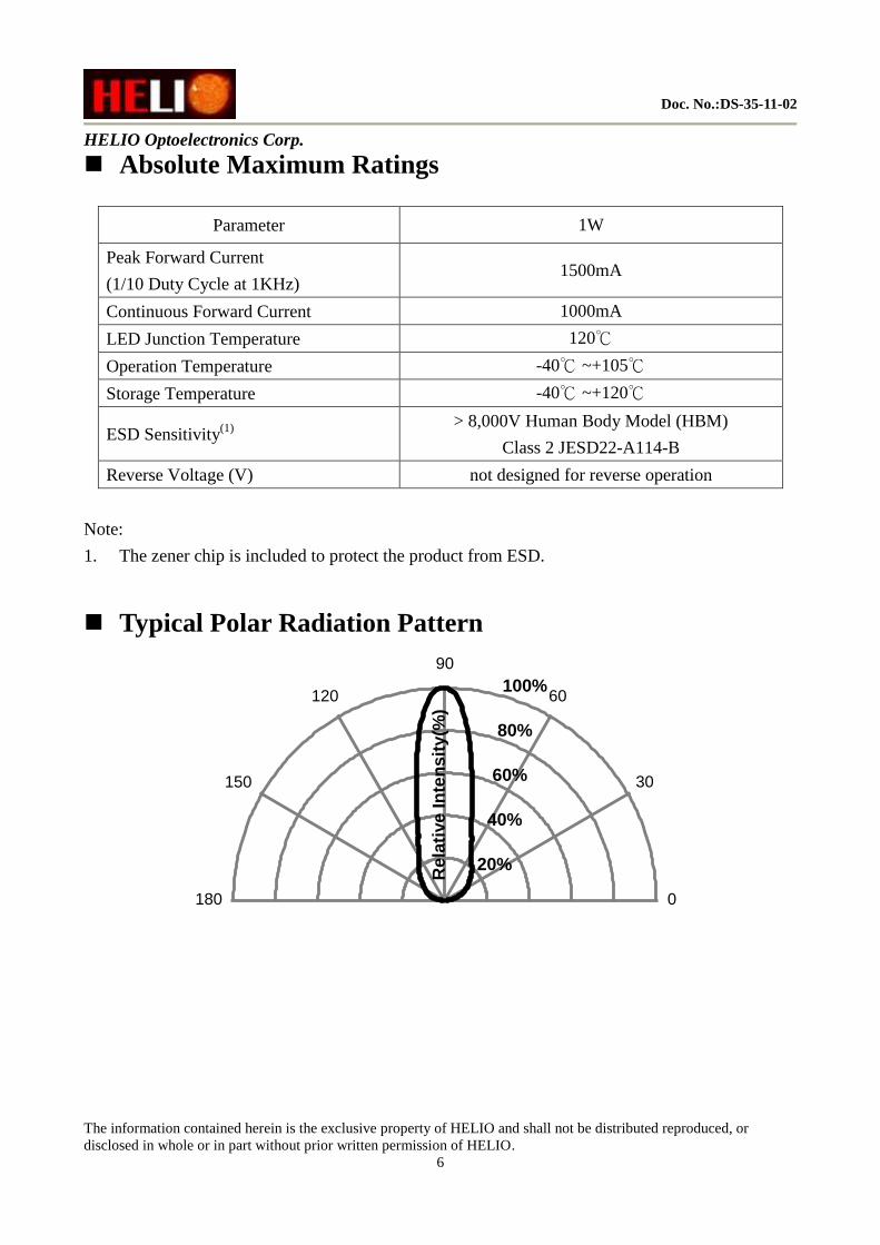
Absolute Maximum Ratings
Parameter 1W
Peak Forward Current
(1/10 Duty Cycle at 1KHz) 1500mA
Continuous Forward Current 1000mA
LED Junction Temperature 120℃
Operation Temperature -40℃ ~+105℃
Storage Temperature -40℃ ~+120℃
ESD Sensitivity(1)
> 8,000V Human Body Model (HBM)
Class 2 JESD22-A114-B
Reverse Voltage (V) not designed for reverse operation
Note:
1. The zener chip is included to protect the product from ESD.
Typical Polar Radiation Pattern
0
30
60
90
120
150
180
R
ela
tive In
ten
sit
y(%
)
100%
80%
60%
40%
20%
Doc. No.:DS-35-11-02
HELIO Optoelectronics Corp.
The information contained herein is the exclusive property of HELIO and shall not be distributed reproduced, or
disclosed in whole or in part without prior written permission of HELIO.
7
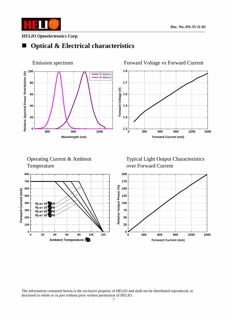
Optical & Electrical characteristics
Emission spectrum Forward Voltage vs Forward Current
800 900 10000
20
40
60
80
100
Re
lati
ve
Sp
ec
tra
l P
ow
er
Dis
trib
uti
on
(%
)
Wavelength (nm)
IR 940nm
IR 850nm
0 300 600 900 1200 15001.3
1.4
1.5
1.6
1.7
1.8
Fo
rward
Vo
ltag
e (
V)
Forward Current (mA)
Operating Current & Ambient Typical Light Output Characteristics
Temperature over Forward Current
0 20 40 60 80 100 1200
100
200
300
400
500
600
700
800
Rj-a= 15 ℃/W
Rj-a= 20 ℃/W
Rj-a= 25 ℃/W
Rj-a= 30 ℃/W
Fo
rwa
rd C
urr
en
t (m
A)
Ambient Temperature (℃)
0 300 600 900 1200 15000
25
50
75
100
125
150
175
200
Re
lati
ve
Ou
tpu
t P
ow
er
(%)
Forward Current (mA)
Doc. No.:DS-35-11-02
HELIO Optoelectronics Corp.
The information contained herein is the exclusive property of HELIO and shall not be distributed reproduced, or
disclosed in whole or in part without prior written permission of HELIO.
8
Storage
Do not open the moisture proof bag before the devices are ready to use. Before the package is opened, LEDs should be stored at temperatures less than 30℃ and
humidity less than 50%. After the package is opened, LEDs should be stored at temperatures less than 30℃ and
humidity less than 30%. LEDs should be used within 168 hours (7 days) after the package is opened. Before using LEDs, baking treatment should be implemented based on the following
conditions: pre-curing at 60±5℃ for 24 hours.

Doc. No.:DS-35-11-02
HELIO Optoelectronics Corp.
The information contained herein is the exclusive property of HELIO and shall not be distributed reproduced, or
disclosed in whole or in part without prior written permission of HELIO.
9
Handling Precaution The softness and dust affinity of silicone molding lens constrain the handling of LED. Thus, some
handling indications of HELIXEON emitters are presented for possible damage prevention and
excellent reliability.
Avoid leaving fingerprints or scratches (by sharp tools) on the silicone resin parts.
Do not force over 2000g impact or pressure on the silicone molding lens.
The LEDs should only be picked up by making contact with the sides of the LED body.
In case of pick-and-place nozzle for surface mount assembly, avoid directly contacting the
lens with nozzle. The pickup tool was recommended and shown as below.
Units:mm
Doc. No.:DS-35-11-02
HELIO Optoelectronics Corp.
The information contained herein is the exclusive property of HELIO and shall not be distributed reproduced, or
disclosed in whole or in part without prior written permission of HELIO.
10
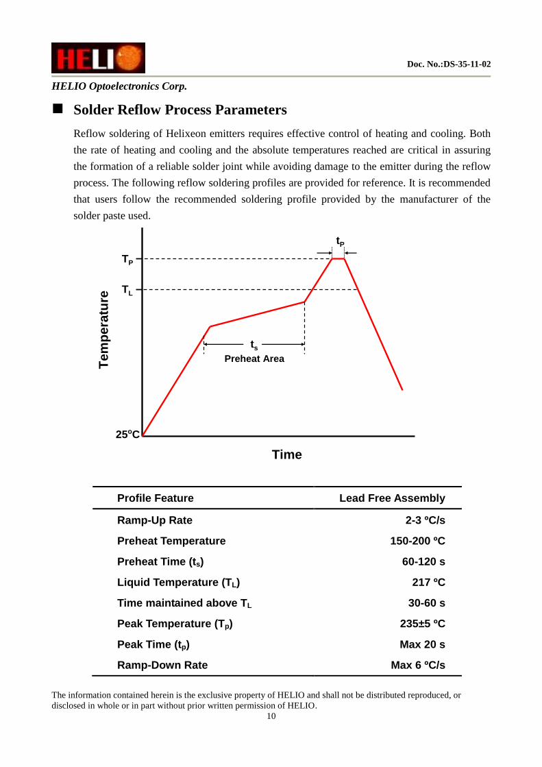
Solder Reflow Process Parameters
Reflow soldering of Helixeon emitters requires effective control of heating and cooling. Both
the rate of heating and cooling and the absolute temperatures reached are critical in assuring
the formation of a reliable solder joint while avoiding damage to the emitter during the reflow
process. The following reflow soldering profiles are provided for reference. It is recommended
that users follow the recommended soldering profile provided by the manufacturer of the
solder paste used.
Time
Tem
pera
ture
ts
Preheat Area
TL
TP
25oC
tP
Profile Feature Lead Free Assembly
Ramp-Up Rate 2-3 ºC/s
Preheat Temperature 150-200 ºC
Preheat Time (ts) 60-120 s
Liquid Temperature (TL) 217 ºC
Time maintained above TL 30-60 s
Peak Temperature (Tp) 235±5 ºC
Peak Time (tp) Max 20 s
Ramp-Down Rate Max 6 ºC/s
Doc. No.:DS-35-11-02
HELIO Optoelectronics Corp.
The information contained herein is the exclusive property of HELIO and shall not be distributed reproduced, or
disclosed in whole or in part without prior written permission of HELIO.
11
Reliability Test List
Test Item Standard
Test Method
Test Conditions Note Number of
Damaged
Resistance to
soldering heat
(reflow soldering)
JEITA ED-4701
300 301
Ta=260℃, 10sec.
(Pre treatment 25℃,70%,168hrs.) 2 times 0/10
Solderability
(reflow soldering)
JEITA ED-4701
300 303
Tsld=245±5℃, 3sec.
(Lead Solder)
1 time over
95% 0/10
Steady state
operating life
Ta=25℃, IF = 350mA
Tested with Helio standard circuit board
1000 hrs. 0/10
Steady state
operating life of
high humidity heat
60℃, RH=90%, IF =350mA
Tested with Helio standard circuit board 1000 hrs. 0/10
Temperature cycle JEITA ED-4701
100 105
-40℃ ~ 25℃ ~ 100℃ ~ 25℃
30min. 5min. 30min. 5min. 100 cycles 0/10
Thermal shock JEITA ED-4701
300 307
0℃ ~ 100℃
15sec. 15sec. 20 cycles 0/10
High temperature
storage
JEITA ED-4701
200 201 Ta=100℃ 1000 hrs. 0/10
Low temperature
storage
JEITA ED-4701
200 202 Ta=-40℃ 1000 hrs. 0/10
Vibration 2000 Hz, 2directions 60min. 0/10
Failure Criteria:
Forward Voltage shift :> 200 mV
Luminous Flux degradation :> 30 %
Forward or Reverse Leakage:>10μ A
Doc. No.:DS-35-11-02
HELIO Optoelectronics Corp.
The information contained herein is the exclusive property of HELIO and shall not be distributed reproduced, or
disclosed in whole or in part without prior written permission of HELIO.
12
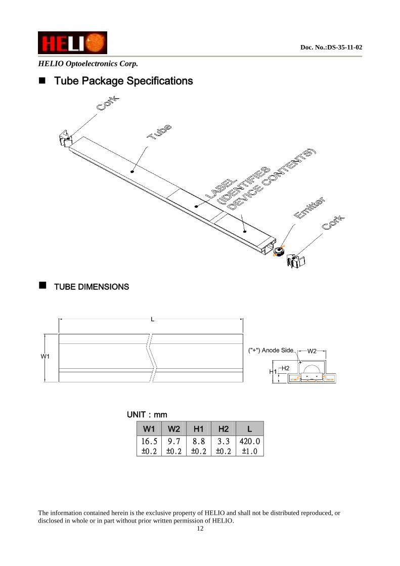
Tube Package Specifications
TUBE DIMENSIONS
UNIT:mm
W1 W2 H1 H2 L
16.5 ±0.2
9.7 ±0.2
8.8 ±0.2
3.3 ±0.2
420.0 ±1.0
Doc. No.:DS-35-11-02
HELIO Optoelectronics Corp.
The information contained herein is the exclusive property of HELIO and shall not be distributed reproduced, or
disclosed in whole or in part without prior written permission of HELIO.
13
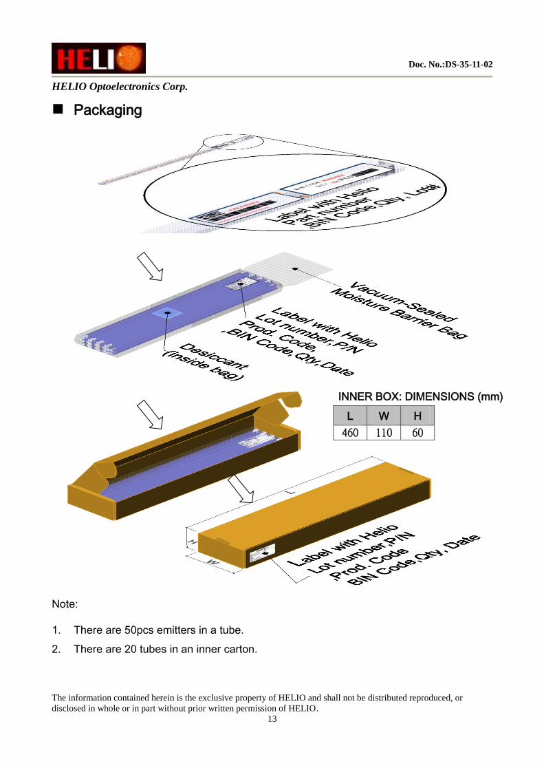
Packaging
Note:
1. There are 50pcs emitters in a tube.
2. There are 20 tubes in an inner carton.
INNER BOX: DIMENSIONS (mm)
L W H
460 110 60
Doc. No.:DS-35-11-02
HELIO Optoelectronics Corp.
The information contained herein is the exclusive property of HELIO and shall not be distributed reproduced, or
disclosed in whole or in part without prior written permission of HELIO.
14
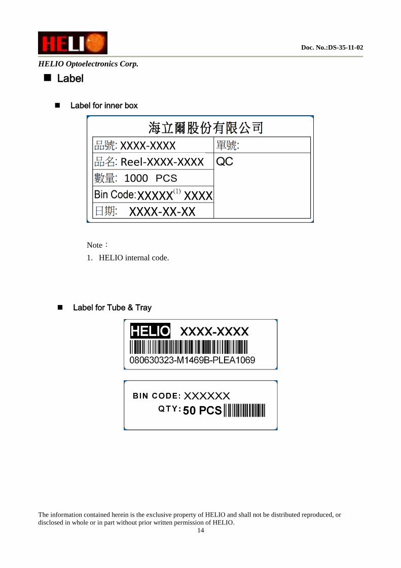
Label
Label for inner box
XXXX-XXXX
XXXXX(1)
XXXX XXXX-XX-XX
Reel-XXXX-XXXX
1000
Note:
1. HELIO internal code.
Label for Tube & Tray
XXXXXX
XXXX-XXXX