high bandwidth automotive power supply for low-cost … papers/016 - norpie2004... · high...
TRANSCRIPT
1
High Bandwidth Automotive Power Supply for Low-cost PWM Audio Amplifiers
Mikkel C. W. Høyerby
Ørsted/DTU Building 325
Dk-2800 Lyngby Denmark
Dennis R. Andersen Ørsted/DTU Building 325
Dk-2800 Lyngby Denmark
Michael A. E. Andersen Ørsted/DTU Building 325
Dk-2800 Lyngby Denmark
Lars Petersen Bang & Olufsen ICEpower
a/s Gl. Lundtoftevej 1b
Dk-2800 Lyngby Denmark
[email protected] Abstract - This paper presents the derivation of a practical solution for constructing a signal tracking power supply for single-ended switching audio amplifiers, motivated by requirements for reduced EMI. The cause and effects of ‘supply pumping’ in single-ended switching amplifiers are investigated, and simulation results for a power supply to meet the specified demands are presented, as well as the results obtained from the constructed prototype.
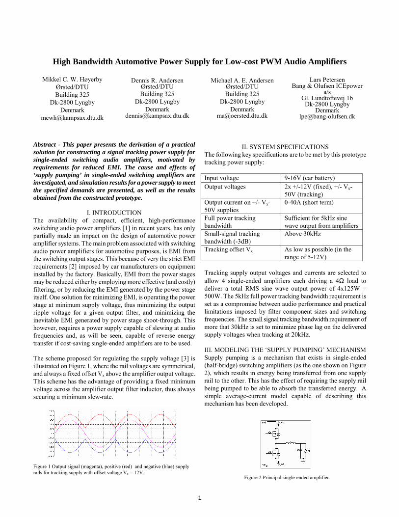
I. INTRODUCTION The availability of compact, efficient, high-performance switching audio power amplifiers [1] in recent years, has only partially made an impact on the design of automotive power amplifier systems. The main problem associated with switching audio power amplifiers for automotive purposes, is EMI from the switching output stages. This because of very the strict EMI requirements [2] imposed by car manufacturers on equipment installed by the factory. Basically, EMI from the power stages may be reduced either by employing more effective (and costly) filtering, or by reducing the EMI generated by the power stage itself. One solution for minimizing EMI, is operating the power stage at minimum supply voltage, thus minimizing the output ripple voltage for a given output filter, and minimizing the inevitable EMI generated by power stage shoot-through. This however, requires a power supply capable of slewing at audio frequencies and, as will be seen, capable of reverse energy transfer if cost-saving single-ended amplifiers are to be used. The scheme proposed for regulating the supply voltage [3] is illustrated on Figure 1, where the rail voltages are symmetrical, and always a fixed offset Vx above the amplifier output voltage. This scheme has the advantage of providing a fixed minimum voltage across the amplifier output filter inductor, thus always securing a minimum slew-rate.
II. SYSTEM SPECIFICATIONS
The following key specifications are to be met by this prototype tracking power supply: Input voltage 9-16V (car battery) Output voltages 2x +/-12V (fixed), +/- Vx-
50V (tracking) Output current on +/- Vx-50V supplies
0-40A (short term)
Full power tracking bandwidth
Sufficient for 5kHz sine wave output from amplifiers
Small-signal tracking bandwidth (-3dB)
Above 30kHz
Tracking offset Vx As low as possible (in the range of 5-12V)
Tracking supply output voltages and currents are selected to allow 4 single-ended amplifiers each driving a 4Ω load to deliver a total RMS sine wave output power of 4x125W = 500W. The 5kHz full power tracking bandwidth requirement is set as a compromise between audio performance and practical limitations imposed by filter component sizes and switching frequencies. The small signal tracking bandwidth requirement of more that 30kHz is set to minimize phase lag on the delivered supply voltages when tracking at 20kHz. III. MODELING THE ‘SUPPLY PUMPING’ MECHANISM Supply pumping is a mechanism that exists in single-ended (half-bridge) switching amplifiers (as the one shown on Figure 2), which results in energy being transferred from one supply rail to the other. This has the effect of requiring the supply rail being pumped to be able to absorb the transferred energy. A simple average-current model capable of describing this mechanism has been developed.
Figure 1 Output signal (magenta), positive (red) and negative (blue) supply rails for tracking supply with offset voltage Vx = 12V.
Figure 2 Principal single-ended amplifier.

2
For a sinusoidal output voltage with amplitude A, it can be shown that the average current in Q1 is:
( ) ( )
+=
sLavgQ V
ftAR
ftAI ππ 2sin12
2sin,1
If the supply voltage is controlled so that it follows the output voltage with a fixed offset Vx, the average current in Q1 becomes:
( ) ( )( )
++=
ftAVftA
RftAI
xLavgQ π
ππ2sin
2sin12
2sin,1
The found expressions for the positive supply current are plotted in Figure 3 for various output levels. The load resistance is set to 1Ω, modeling 4 amplifiers each driving a 4Ω load, operated from the same rails, with identical output signals.
Fixed supply (+/-50V)
Tracking supply, Vx =12V
Tracking supply, Vx =5V
Figure 3 Calculated positive supply currents for single-ended amplifier, RL = 1Ω, f=20Hz, for A=35V (red), A=20V(blue) and A=10V(green).
The results on Figure 3 show that the ‘supply pumping’ current from a +/-50V amplifier can be reduced by employing a tracking power supply, but low values of Vx are required for substantial reduction. This will influence the requirements for control bandwidth and filter component size in the power supply, in general a low value of Vx will require smaller filter components and greater closed-loop bandwidth for the power supply. In addition, low values of Vx impose value restrictions on the amplifier output filter components, if a minimal amplifier slew-rate is to be ensured.
IV. PROPOSED POWER CONVERSION SCHEME
The tracking power supply for the single-ended amplifiers must fulfill the following key requirements:
• High output voltage slew rate (as required by the audio signal) => High control bandwidth
• Ability to deal with ‘supply pumping’ current • High transient output current capacity
All these requirements can be fulfilled by the 2-stage solution shown on Figure 4, with an isolated low-bandwidth pre-converter for providing fixed high voltage (e.g. +/-50V) rails, followed by separate high-bandwidth buck converters on each rail to provide the correct supply voltages for the amplifiers. To minimize EMI problems, a boost topology is employed for the pre-converter. A standard single-inductor push-pull boost converter is chosen over a seemingly advantageous [4] dual-inductor boost converter, due to its much lower minimum input power with a given boost inductor [9]. The buck converters, when implemented with synchronous rectifiers (Q4 and Q6), have the ability to reverse their output currents, thus providing a path for the inevitable ‘supply pumping’ currents. This is essential, since the filter capacitors for each Vs rail (C2 and C4) including decoupling for the amplifiers, may be no more than approximately 10µF (with 5µH for L2 and L3) to allow sufficient Vs slew rate.
Figure 4 Principal topology for tracking power supply for single ended amplifier system
Each bulk capacitors (C1 and C3) must be able to store the energy from the ‘supply pumping’, which is maximal for minimum signal frequencies. It can be shown that the charge delivered to C1 because of ‘supply pumping’ during the negative period with a sinusoidal output voltage waveform, is:
Lb
x
RfVAVQ
π2=∆
Which is useful for finding an appropriate value of C1. Low values of Vx are seen to reduce the demands on the capacitance of C1, as expected from results on Figure 3.
V. PROPOSED CONTROL SCHEME A number of possible schemes exist for realizing high-bandwidth controllers for the buck converters [5]. One of the fastest classes of switching power supply control systems available is self-oscillating (asynchronous) hysteretic control

3
[5], which can also be employed in amplifiers [6] with excellent results. When combined with current control, hysteretic control [7] can provide the high bandwidth and fast transient response required for the tracking converters. With current control, the inductor dynamics are avoided in the small-signal design of the voltage loop, an advantage since the filter frequency is well within the targeted control bandwidth.
Figure 5 Principal structure of proposed control scheme for tracking
converters.
Hysteretic current control requires sensing of the inductor current, where sensing the high-side switch current would suffice with a standard peak-current mode controller. Relocating the current sensing resistor to the output side of the filter inductor results in problems with common-mode rejection in the sense amplifier, since significant HF (ripple) and LF (audio) common-mode voltages need rejection. Estimating the inductor current by integrating the inductor voltage is a different approach that eliminates the loss and expense of the current sensing resistor. Again, common-mode rejection of the differential sense amplifier is critical. An inexpensive sense winding on the inductor [8] represents a much easier way of obtaining the differential inductor voltage, as an additional advantage the sensed voltage is floating, minimizing measurement noise problems. The discussed methods are illustrated on Figure 6.
1. Current measurement using a sensing resistor
2. Current estimation by inductor voltage integration
3. Current estimation by inductor sense winding voltage integration
Figure 6 Different methods for obtaining the inductor current in a buck converter
Feedback of the inductor current estimate, rather than the true inductor current causes alteration of the closed-loop characteristics of the current control loop [9]. Specifically, the inductor current estimate cannot be correct at DC, due to the input offset voltage of any integrator, resulting in the absence of current feedback at low frequencies. The model of power stage, output filter and current loop with current estimation shown on Figure 7 has been used to assess the effects of limited integrator DC performance. The parameters in the model shown, with used values, are: Output filter inductance
L 5µH
Output filter capacitance
C 10µH
Load resistance Rs Variable Inductor winding ratio nsense/ninductor
nL 1:12
‘Integration’ time constant
τi 12µs
Lower cut-off time constant
τc Variable
PWM modulator gain Kmod 10
Figure 7 Model of current controlled buck converter with inductor current estimation.
The closed-loop transfer function from current reference input to output voltage, )(sGcl , is:
CsRRsGsG
s
sIcl +
⋅=1
)()( ,
where the transfer function from current reference to average inductor current, )(sGI , is given by:
)()()())(1(
)( 3mod
2mod
2mod
CLRsCRnKCLRLsnKRLsRCRsCRsK
sGscsicLscicLcss
cscsI τττττττ
ττ+++++++
+++=

4
Bode plots of Gcl(s) with varying Rs and τc are shown on Figure 8. The transition from current mode to voltage mode control when τc is shortened is evident.
Figure 8 Closed-loop bode plots for current loop in buck converter with inductor current estimation, with τc≈∞ (top left), τc=1s (top right), τc=1ms (bottom left) and τc≈0s (bottom right)
With the information on the frequency characteristics of the closed current loop, an output voltage controller can be designed. It is designed around a lag compensator for moving the output filter pole at Rs=1Ω from 16kHz to 10kHz, and incorporates low frequency integration for setting the DC operating point of the current loop correctly.
VI. SIMULATED RESULTS A switching simulation model of the tracking converters is constructed, with the following key parameters:
Buck filter inductor (L2/L3) 5µH Buck filter capacitance (C2/C3)
10µF
Buck supply rails (+/-Vb) +/-60V Load type Switching amplifier
model, RL = 1Ω Switching frequency (nominal)
~ 300kHz
Inductor current ripple 4A (peak) Each converter is fitted with the proposed control system, with compensator blocks tuned to minimize static and dynamic errors, while maintaining stability. Initially, full-power bandwidth is examined. It becomes evident, as seen on Figure 9, that the required 5kHz can be met with Vx greater than 10V, if a minimum of difference of 5V between Vs and Vout is required for the amplifier to function properly. Limiting the negative slew rate of Vs allows the full-power bandwidth test to be passed with slightly lower values of Vx. This is shown on Figure 10, where a 1ms decay time constant is placed on Vref. The small-signal bandwidth of the control system is tested using
a multi-tone input signal, corresponding to an amplifier output voltage with a 30Vpeak, 1kHz component, and a 10Vpeak 20kHz component, amplitude modulated with a 10Vpeak 3kHz sine wave. This is an attempt to model a realistic audio signal. Figure 11 and Figure 12 show the results with this signal, with Vx = 10V, and Vx = 7V, plus 1ms decay time constant, respectively. With a Vx = 10V, the control system performs excellently, with minimal phase lag, even when tracking the 20kHz component. The decay time constant now has a negative influence on tracking behaviour, because it causes sharp ‘edges’ on the reference signal, as seen on Figure 12. If the decay time constant is removed, the tracking function better with the compound signal, as Figure 13 shows for Vx = 7V. The tracking power supply is open-load stable, as shown by the simulation in Figure 14, where both supply rails are stable during the transition from loaded to unloaded state. This is due
Figure 9 Simulated Vout (green) and +/-Vs (red/blue), Vx = 10V. Full power 5kHz output signal.
Figure 10 Simulated Vout (green) and +/-Vs (red/blue), Vx = 7V. Full power 5kHz output signal, 1ms decay time constant.
Figure 11 Simulated Vout (green) and +/-Vs (red/blue), Vx = 10V. Compound 1/3/20kHz signal.
Figure 12 Simulated Vout (green) and +/-Vs (red/blue), Vx = 7V, 1ms decay time constant. Compound 1/3/20kHz signal.
Figure 13 Simulated Vout (green) and +/-Vs (red/blue), Vx = 7V. Compound 1/3/20kHz signal.
Figure 14 Simulated Vout (green) and +/-Vs (red/blue), Vx = 7V. Half-wave 5kHz sine wave.

5
to the Zobel networks connected across each Vs rail. Power loss in the Zobel networks is low, comparable to similar networks used to ensure open-load stability in switching amplifiers.
VII. ACHIEVED PRACTICAL RESULTS A functional prototype power supply has been implemented as shown on Figure 15.
Figure 15 Implemented prototype tracking power supply
Conducted EMI performance of the push-pull boost section of the supply has been examined by measurement of the input current during CCM operation, as shown on Figure 16.
The conducted EMI demands imposed by Class 5 of the CISPR-25 automotive EMC standard are listed for each harmonic of the switching frequency in Table 1. This standard imposed no limits below 150kHz, which is the reason for setting the switching frequency to 120kHz.
Harmonic number Class 5 maximum limits 1. (120kHz) Undefined 2. (240kHz) 558µApeak 3.-4.(360-480kHz) Undefined 5. (600kHz) 78µApeak 6. (720kHz) 67µApeak 7. (840kHz) 59µApeak 8. (960kHz) 54µApeak 9. (1080kHz) 52µApeak Table 1 Maximum limits for harmonic input currents imposed by CISPR-25 class 5, recalculated from dBµV to mApeak.
With the measured 4mA peak-peak ripple at 120kHz, the demand for less than 558µA peak at 240kHz should be met with ease. Due to the usage of a 4th order input filter, the following lower harmonics should also be under control. Examination of higher frequency EMI performance would require proper EMI measurement equipment. Efficiency of the implemented push-pull boost converter has been examined, as shown on Figure 17. The real efficiency is less than the calculated efficiency due to control system power consumption at low output powers, and probably due to proximity losses in transformer windings at higher output powers.
Figure 17 Calculated and measured efficiency of implemented push-pull
boost converter
The performance of the current estimation technique employed in the tracking buck converters is evident from Figure 18. The estimated current is virtually noiseless, in phase and proportional to the actual inductor current. This will only occur as long as the permeability of the core remains constant, which is ensured through proper inductor core selection.
Figure 18 Measured inductor current (below, 500mA/div) and estimated
inductor current (above) in tracking buck converter.
The small-signal closed-loop response of the tracking buck converters can be examined from the closed-loop gain-phase measurement shown on Figure 19.
Figure 19 Measured closed-loop gain-phase characteristics of tracking buck converter, unloaded (left) and driving 4Ω (right)
Figure 16 Measured power supply input current during CCM operation of
push-pull boost converter

6
The bandwidth is well above 20kHz, and is in particular unaffected by loading conditions, while the phase lag at 20kHz is minimal at 15°. The current control loop employs the maximum practical value of τc, so that the transition point from current to voltage-mode is around 350Hz. Further examination of control system performance is done by square wave testing, with an example shown on Figure 20. It is concluded that the control system is stable and fast, as required.
Figure 20 Measured tracking buck converter output voltage, 1kHz square
wave into open load
The output voltages of the tracking power supply are measured while driving an amplifier playing a 1kHz sine wave, as shown on Figure 21. The power supply performs the demanded function of tracking the amplifier output voltage.
Figure 21 Measured positive (top) and negative (bottom) tracking supply voltages, plus amplifier output voltage (middle), 1kHz sine wave into 8Ω.
VIII. CONCLUSION It has been demonstrated, that the possibility exists for fitting single-ended switching amplifiers with a high-bandwidth tracking power supply. Good results have been achieved using inductor current estimation, minimizing power losses. Although more complex than a non-tracking supply, the tracking supply offers the opportunity for utilizing less storage capacitance per rail, and most probably reduces EMI at low output levels.
IX. PATENT NOTE The technique of using tracking supply voltages for PWM audio amplifiers (as shown on Figure 1), also known as PAWM (Pulse Amplitude and Width Modulation), is patent pending by Bang & Olufsen ICEpower a/s.
REFERENCES
[1] Karsten Nielsen, “Audio Power Amplifier Techniques with Energy Efficient Power Conversion”, Department of Applied Electronics, DTU, Denmark, May 1998
[2] Ford Motor Company, “Electronic Component EMC Requirements & Test Procedures”, April 1999
[3] Karsten Nielsen, Lars Michael Fenger, “The Active pulse modulated Transducer (AT) A novel audio power conversion system architecture”, 115th AES Convention, New York, October 2003
[4] Wilson C. P. de Aragão Filho, Ivo Barbi, ”A Comparison Between two Current-Fed Push-Pull DC-DC Converters – Analysis, Design and Experimentation”, IEEE International Telecommunication Energy Conf. Proc. Rec., pp 313-320, 1996
[5] Rais Miftakhutdinov, “An Analytical Comparison of Alternative Control Techniques for Powering Next-Generation Microprocessors”, 2001
[6] Paul van der Hulst, André Veltman, René Groenberg, ”An asynchronous switching high-end power amplifier”, 112th AES Convention, Munich, Germany, May 2002
[7] Robert W. Erickson, Dragan Maksimovic, “Fundamentals of Power Electronics, 2nd ed, p. 657”, 2001
[8] Allen F. Rozman, Jeffrey J. Boylan, ”Band Pass Current Control” – Bell Laboratories AT&T Power Systems 1994
[9] Mikkel C. W. Høyerby, Dennis R. Andersen ”ICEpower Automotive CarFi System” – Master Thesis, Ørsted/DTU, Denmark April 2004