high-k devices by ald for semiconductor applications
TRANSCRIPT

© Fraunhofer
Baltic ALD 2014 conference, Helsinki, May 12-13, 2014
Fraunhofer Institute for Photonic Microsystems
Business Unit Center Nanoelectronic Technologies Dresden (IPMS-CNT)
HIGH-K DEVICES BY ALD FOR SEMICONDUCTOR APPLICATIONS
Jonas Sundqvist, Wenke Weinreich, Johannes Müller, Stefan Riedel, Konrad Seidel , Patrick Polakowski, Malte Czernohorsky
© Fraunhofer
The first high-k devices by ALD for semiconductor applications
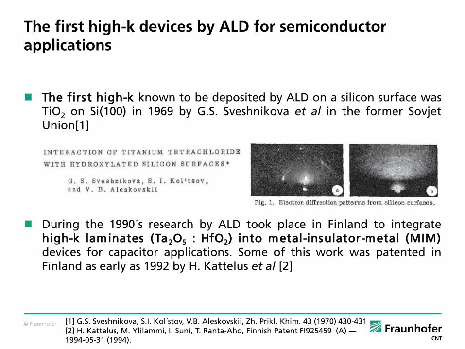
The first high-k known to be deposited by ALD on a silicon surface was TiO2 on Si(100) in 1969 by G.S. Sveshnikova et al in the former Sovjet Union[1]
During the 1990´s research by ALD took place in Finland to integrate high-k laminates (Ta2O5 : HfO2) into metal-insulator-metal (MIM) devices for capacitor applications. Some of this work was patented in Finland as early as 1992 by H. Kattelus et al [2]
[1] G.S. Sveshnikova, S.I. Kol´stov, V.B. Aleskovskii, Zh. Prikl. Khim. 43 (1970) 430-431 [2] H. Kattelus, M. Ylilammi, I. Suni, T. Ranta-Aho, Finnish Patent FI925459 (A) ― 1994-05-31 (1994).

© Fraunhofer
Introduction of high-k devices by ALD for semiconductor applications
Jonas Sundqvist, Baltic ALD 2014 conference, Helsinki, May 12-13, 2014
© Fraunhofer
Outline of recent developments at Fraunhofer CNT
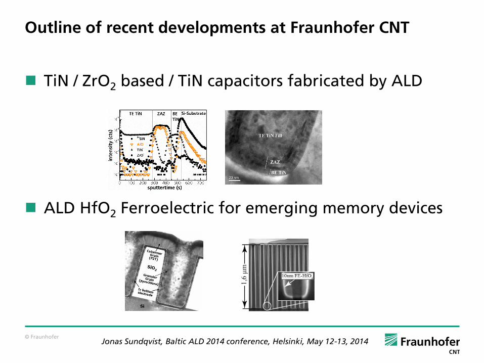
TiN / ZrO2 based / TiN capacitors fabricated by ALD
ALD HfO2 Ferroelectric for emerging memory devices
Jonas Sundqvist, Baltic ALD 2014 conference, Helsinki, May 12-13, 2014
© Fraunhofer
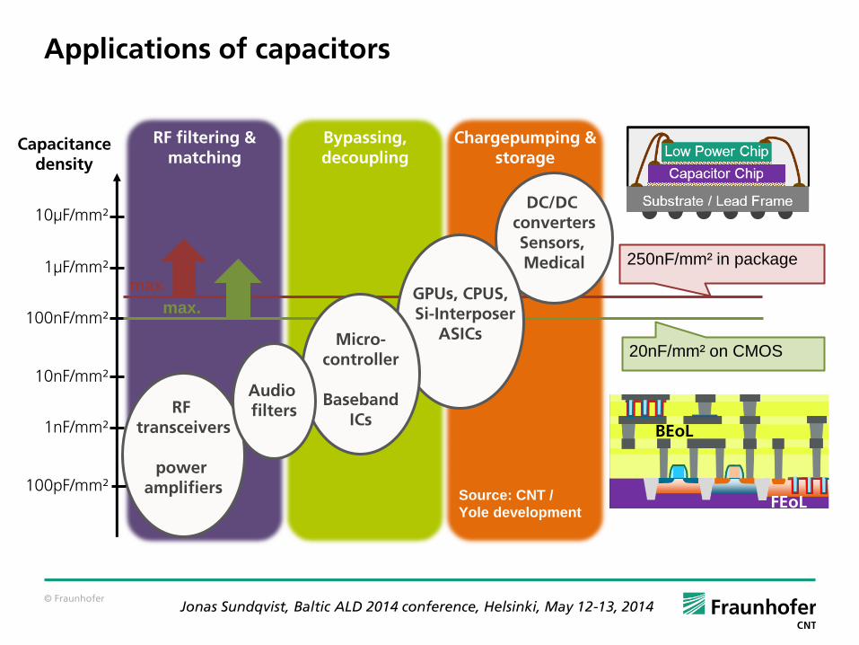
Applications of capacitors
BEoL
100pF/mm²
1nF/mm²
10nF/mm²
100nF/mm²
1µF/mm²
10µF/mm²
RF filtering & matching
Bypassing, decoupling
Chargepumping & storage
RF transceivers
power
amplifiers
250nF/mm² in package
max.
20nF/mm² on CMOS
max.
Capacitance density
Source: CNT /
Yole development
DC/DC converters Sensors, Medical
GPUs, CPUS, Si-Interposer
ASICs
Micro- controller
Baseband
ICs
Audio filters
BEoL
FEoL
BEoL
Jonas Sundqvist, Baltic ALD 2014 conference, Helsinki, May 12-13, 2014
© Fraunhofer
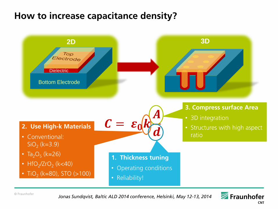
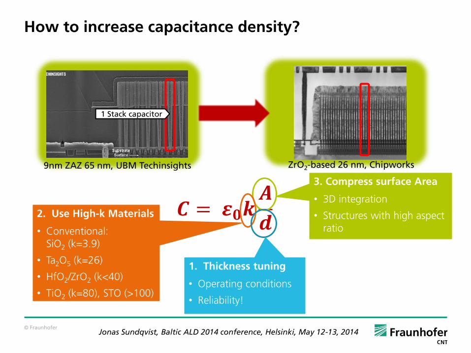
𝑪 = 𝜺𝟎𝒌𝑨
𝒅
Bottom Electrode
Dielectric
2D 3D
3. Compress surface Area
• 3D integration
• Structures with high aspect ratio
2. Use High-k Materials
• Conventional: SiO2 (k=3.9)
• Ta2O5 (k=26)
• HfO2/ZrO2 (k<40)
• TiO2 (k=80), STO (>100)
1. Thickness tuning
• Operating conditions
• Reliability!
How to increase capacitance density?
Jonas Sundqvist, Baltic ALD 2014 conference, Helsinki, May 12-13, 2014
© Fraunhofer
𝑪 = 𝜺𝟎𝒌𝑨
𝒅
3. Compress surface Area
• 3D integration
• Structures with high aspect ratio
2. Use High-k Materials
• Conventional: SiO2 (k=3.9)
• Ta2O5 (k=26)
• HfO2/ZrO2 (k<40)
• TiO2 (k=80), STO (>100)
1. Thickness tuning
• Operating conditions
• Reliability!
9nm ZAZ 65 nm, UBM Techinsights
1 Stack capacitor
ZrO2-based 26 nm, Chipworks
How to increase capacitance density?
Jonas Sundqvist, Baltic ALD 2014 conference, Helsinki, May 12-13, 2014
© Fraunhofer
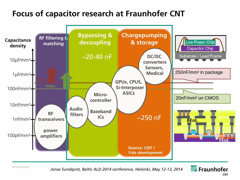
Focus of capacitor research at Fraunhofer CNT
RF filtering & matching
Bypassing & decoupling
BEoL
100pF/mm²
1nF/mm²
10nF/mm²
100nF/mm²
1µF/mm²
10µF/mm²
Chargepumping & storage
RF transceivers
power
amplifiers
250nF/mm² in package
max.
20nF/mm² on CMOS
max.
Capacitance density
Source: CNT /
Yole development
DC/DC converters Sensors, Medical
GPUs, CPUS, Si-Interposer
ASICs
Micro- controller
Baseband
ICs
Audio filters
BEoL
FEoL
BEoL
~20-40 nF
~250 nF
Jonas Sundqvist, Baltic ALD 2014 conference, Helsinki, May 12-13, 2014
© Fraunhofer
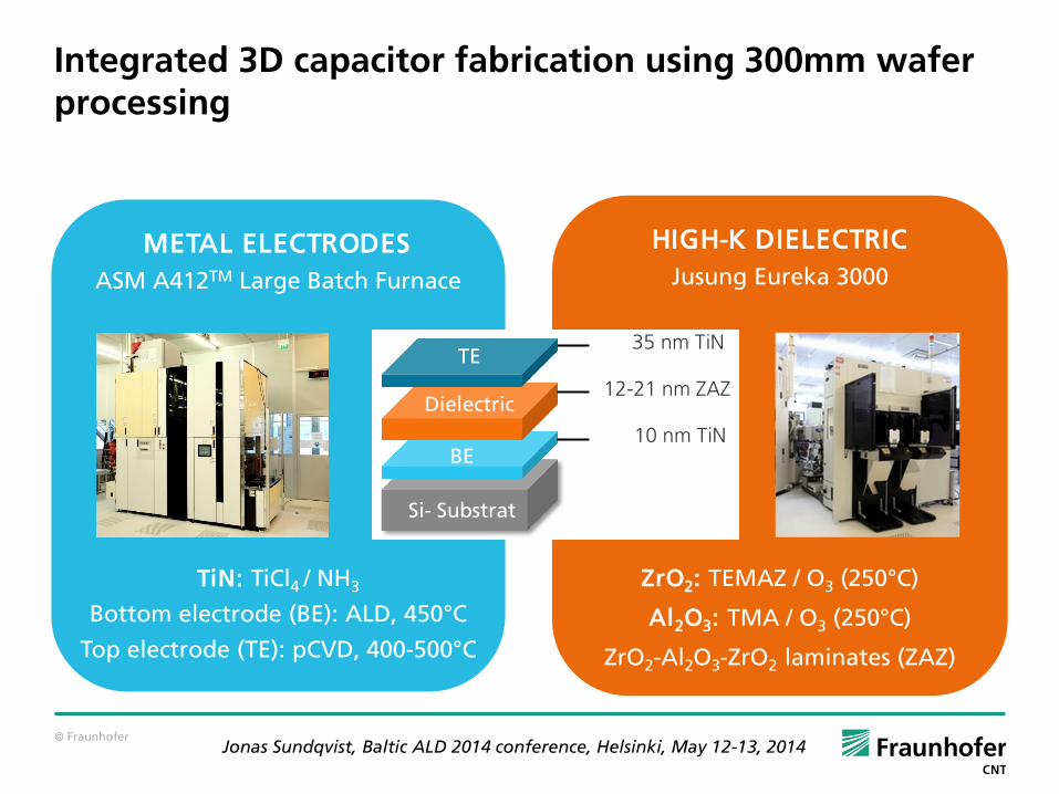
Integrated 3D capacitor fabrication using 300mm wafer processing
HIGH-K DIELECTRIC
Jusung Eureka 3000
ZrO2: TEMAZ / O3 (250°C)
Al2O3: TMA / O3 (250°C)
ZrO2-Al2O3-ZrO2 laminates (ZAZ)
METAL ELECTRODES
ASM A412TM Large Batch Furnace
TiN: TiCl4 / NH3
Bottom electrode (BE): ALD, 450°C
Top electrode (TE): pCVD, 400-500°C
35 nm TiN
10 nm TiN
Dielectric
BE
Si- Substrat
12-21 nm ZAZ
TE
Jonas Sundqvist, Baltic ALD 2014 conference, Helsinki, May 12-13, 2014
© Fraunhofer
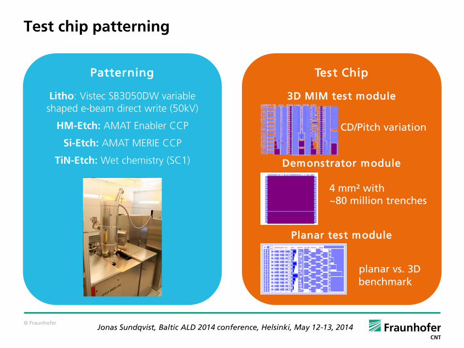
Test chip patterning
Test Chip
3D MIM test module
CD/Pitch variation
Demonstrator module
4 mm² with ~80 million trenches
Planar test module
planar vs. 3D benchmark
Patterning
Litho: Vistec SB3050DW variable shaped e-beam direct write (50kV)
HM-Etch: AMAT Enabler CCP
Si-Etch: AMAT MERIE CCP
TiN-Etch: Wet chemistry (SC1)
Jonas Sundqvist, Baltic ALD 2014 conference, Helsinki, May 12-13, 2014
© Fraunhofer
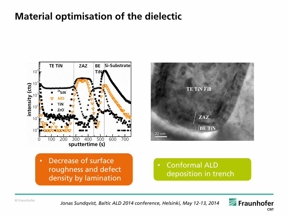
Material optimisation of the dielectic
• Conformal ALD deposition in trench
• Decrease of surface roughness and defect density by lamination
Jonas Sundqvist, Baltic ALD 2014 conference, Helsinki, May 12-13, 2014

© Fraunhofer
• Failures at high temperatures
• Leakage and lifetime improvement by lowering TE to 400°C
TiN
– 5
00 °
C ZAZ
22 nm ZAZ
11 nm TiN
-3 -2 -1 0 1 2 310-11
10-10
10-9
10-8
10-7
10-6
10-5
15 nm ZAZ 450 °C 400 °C
18 nm ZAZ 450 °C 400 °C
Cu
rren
t D
en
sity
(A
/cm
²)
Voltage (V)
1.0 1.5 2.0 2.5 3.0 3.5100
101
102
103
104
105
106
107
108
109
Tim
e t
o B
reakd
ow
n (
s)
Electric Field (MV/cm)
10 years
15 nm ZAZ 400 °C 450 °C
18 nm ZAZ 400 °C 450 °C
Material optimisation of the metal nitride electrode
Jonas Sundqvist, Baltic ALD 2014 conference, Helsinki, May 12-13, 2014
© Fraunhofer
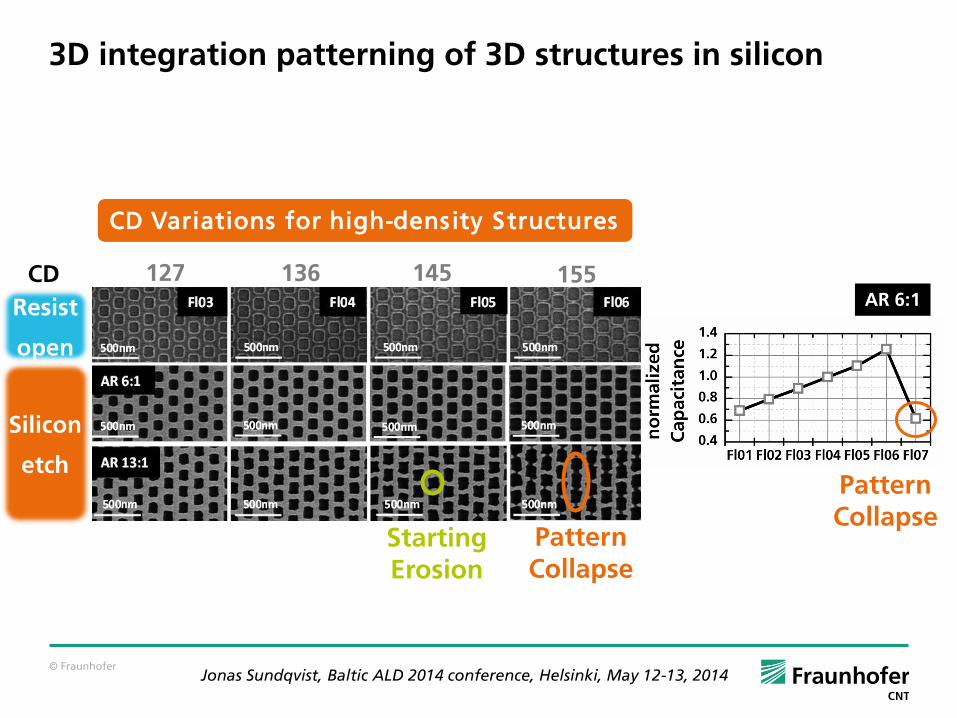
3D integration patterning of 3D structures in silicon
Resist
open
Silicon
etch
Starting Erosion
Pattern Collapse
AR 6:1
Pattern Collapse
127 136 145 155 CD
CD Variations for high-density Structures
Jonas Sundqvist, Baltic ALD 2014 conference, Helsinki, May 12-13, 2014
© Fraunhofer
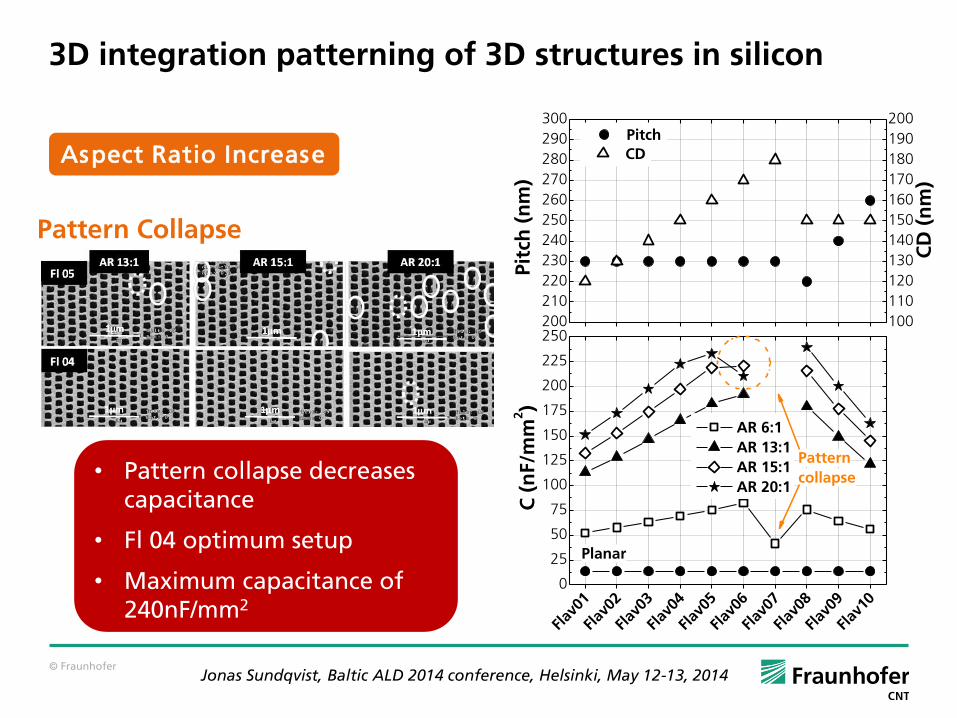
3D integration patterning of 3D structures in silicon
• Pattern collapse decreases capacitance
• Fl 04 optimum setup
• Maximum capacitance of 240nF/mm2
Pattern Collapse
Aspect Ratio Increase
200
210
220
230
240
250
260
270
280
290
300
Flav
01
Flav
02
Flav
03
Flav
04
Flav
05
Flav
06
Flav
07
Flav
08
Flav
09
Flav
100
25
50
75
100
125
150
175
200
225
250
Pitch
Pit
ch (
nm
)
100
110
120
130
140
150
160
170
180
190
200
CD
(n
m)
CD
C (
nF/m
m2)
AR 6:1
AR 13:1
AR 15:1
AR 20:1
Pattern
collapse
Planar
Jonas Sundqvist, Baltic ALD 2014 conference, Helsinki, May 12-13, 2014
© Fraunhofer
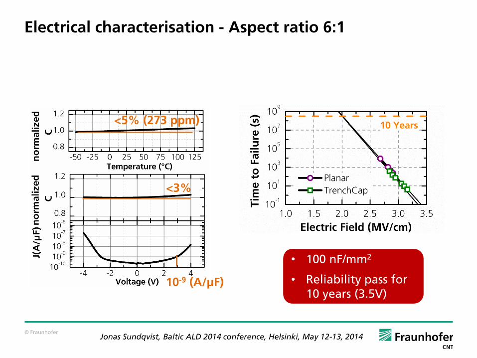
Electrical characterisation - Aspect ratio 6:1
• 100 nF/mm2
• Reliability pass for 10 years (3.5V)
<3% • 100 nF/mm2
• Reliability pass for 10 years (3.5V)
<5% (273 ppm)
10-9 (A/µF)
Jonas Sundqvist, Baltic ALD 2014 conference, Helsinki, May 12-13, 2014
© Fraunhofer
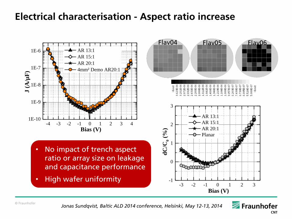
Electrical characterisation - Aspect ratio increase
Flav04 Flav05 Flav06
• No impact of trench aspect ratio or array size on leakage and capacitance performance
• High wafer uniformity
-4 -3 -2 -1 0 1 2 3 41E-10
1E-9
1E-8
1E-7
1E-6 AR 13:1
AR 15:1
AR 20:1
4mm² Demo AR20:1
J (
A/µ
F)
Bias (V)
-3 -2 -1 0 1 2 3-1
0
1
2
3
dC
/C0 (
%)
Bias (V)
AR 13:1
AR 15:1
AR 20:1
Planar
Jonas Sundqvist, Baltic ALD 2014 conference, Helsinki, May 12-13, 2014
© Fraunhofer
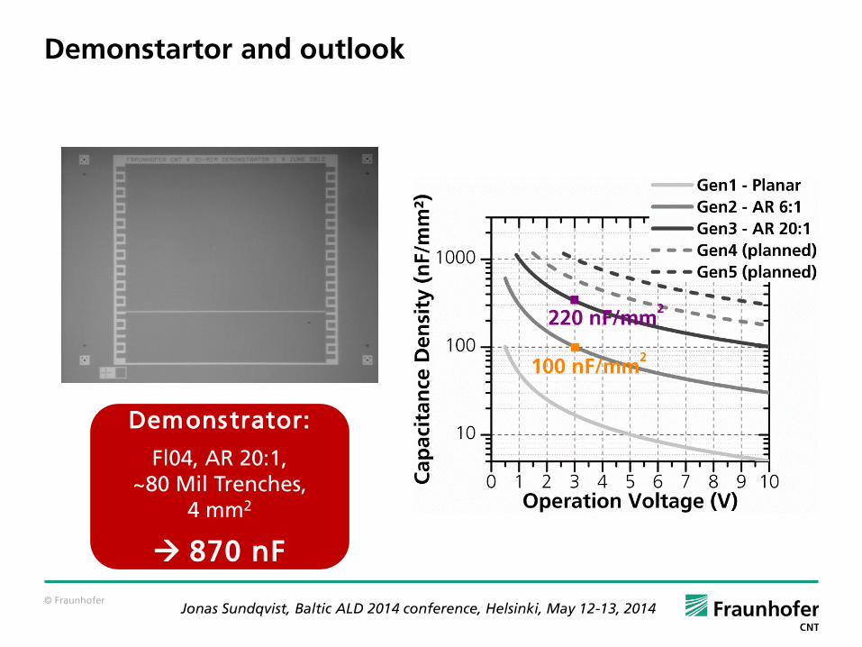
Demonstrator:
Fl04, AR 20:1, ~80 Mil Trenches,
4 mm2
870 nF
Demonstartor and outlook
Jonas Sundqvist, Baltic ALD 2014 conference, Helsinki, May 12-13, 2014
© Fraunhofer
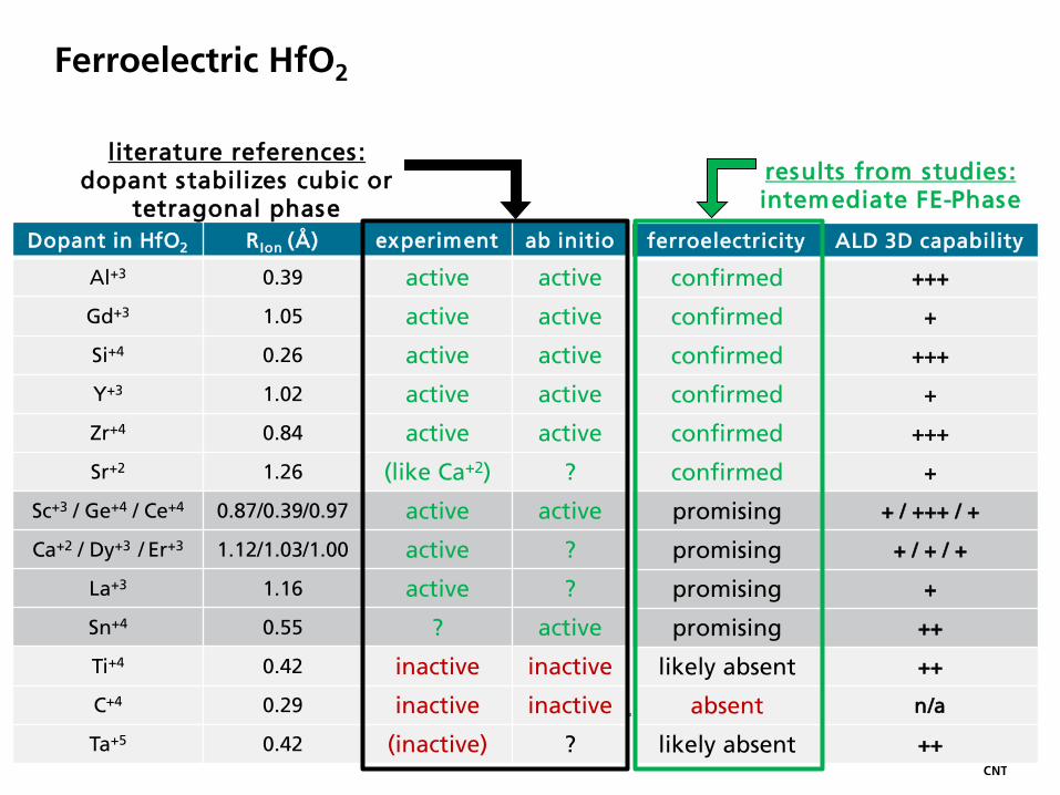
Ferroelectric HfO2
Dopant in HfO2 R Ion (Å) experiment ab initio
Al+3 0.39 active active
Gd+3 1.05 active active
Si+4 0.26 active active
Y+3 1.02 active active
Zr+4 0.84 active active
Sr+2 1.26 (like Ca+2) ?
Sc+3 / Ge+4 / Ce+4 0.87/0.39/0.97 active active
Ca+2 / Dy+3 / Er+3 1.12/1.03/1.00 active ?
La+3 1.16 active ?
Sn+4 0.55 ? active
Ti+4 0.42 inactive inactive
C+4 0.29 inactive inactive
Ta+5 0.42 (inactive) ?
literature references : dopant stabilizes cubic or
tetragonal phase
results from studies : intemediate FE-Phase
ferroelectricity ALD 3D capability
confirmed +++
confirmed +
confirmed +++
confirmed +
confirmed +++
confirmed +
promising + / +++ / +
promising + / + / +
promising +
promising ++
likely absent ++
absent n/a
likely absent ++
© Fraunhofer
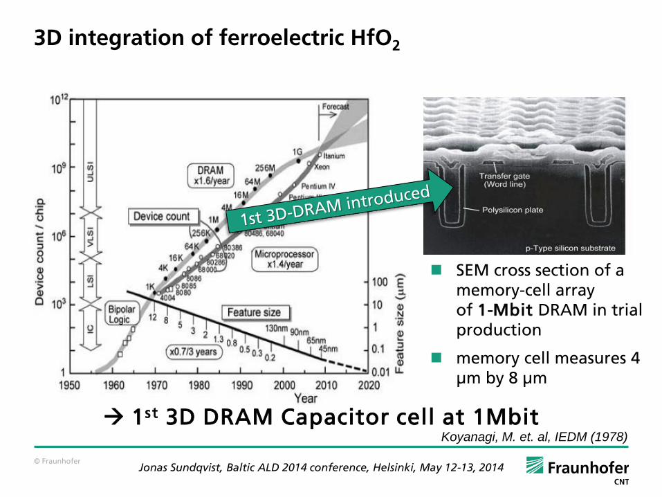
3D integration of ferroelectric HfO2
Koyanagi, M. et. al, IEDM (1978)
SEM cross section of a memory-cell array of 1-Mbit DRAM in trial production
memory cell measures 4 μm by 8 μm
1st 3D DRAM Capacitor cell at 1Mbit
Jonas Sundqvist, Baltic ALD 2014 conference, Helsinki, May 12-13, 2014
© Fraunhofer
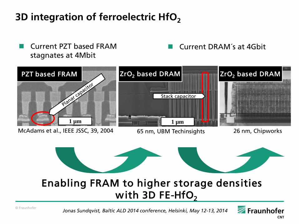
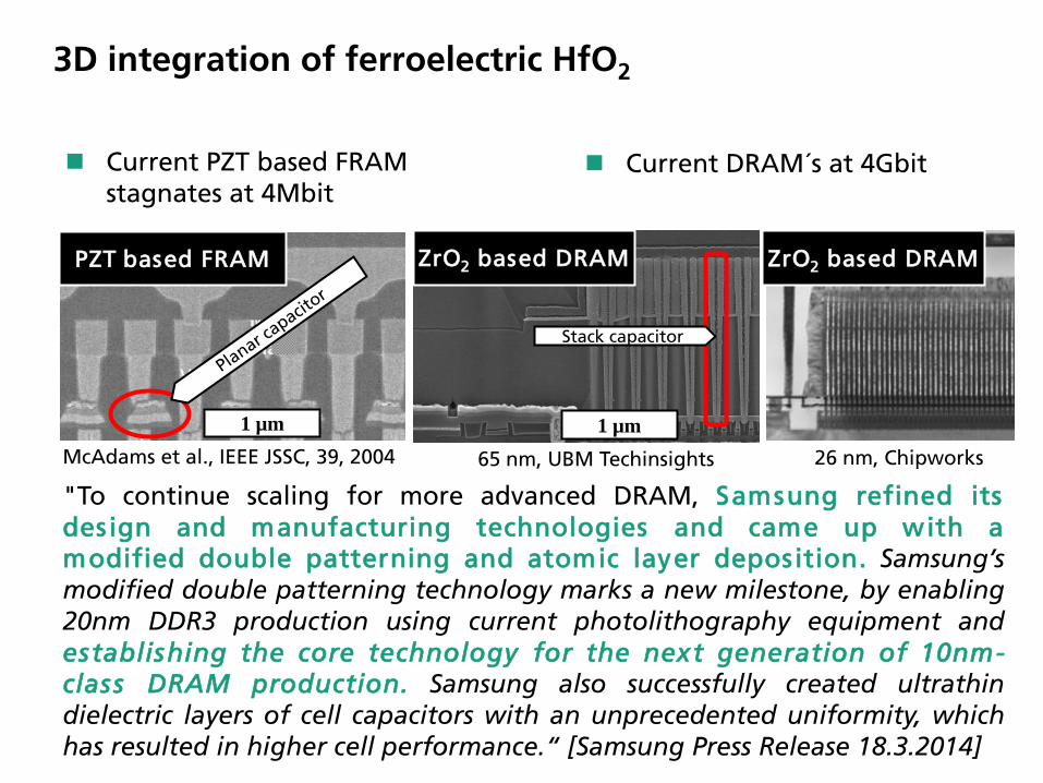
3D integration of ferroelectric HfO2
McAdams et al., IEEE JSSC, 39, 2004
PZT based FRAM
1 µm
65 nm, UBM Techinsights
ZrO2 based DRAM
1 µm
Stack capacitor
Current PZT based FRAM stagnates at 4Mbit
Current DRAM´s at 4Gbit
Enabling FRAM to higher storage densities with 3D FE-HfO2
26 nm, Chipworks
ZrO2 based DRAM
Jonas Sundqvist, Baltic ALD 2014 conference, Helsinki, May 12-13, 2014
© Fraunhofer
3D integration of ferroelectric HfO2
McAdams et al., IEEE JSSC, 39, 2004
PZT based FRAM
1 µm
65 nm, UBM Techinsights
ZrO2 based DRAM
1 µm
Stack capacitor
Current PZT based FRAM stagnates at 4Mbit
Current DRAM´s at 4Gbit
26 nm, Chipworks
ZrO2 based DRAM
"To continue scaling for more advanced DRAM, Samsung refined its des ign and manufacturing technologies and came up with a modified double patterning and atomic layer deposition. Samsung’s modified double patterning technology marks a new milestone, by enabling 20nm DDR3 production using current photolithography equipment and establishing the core technology for the next generation of 10nm-class DRAM production. Samsung also successfully created ultrathin dielectric layers of cell capacitors with an unprecedented uniformity, which has resulted in higher cell performance.“ [Samsung Press Release 18.3.2014]
© Fraunhofer
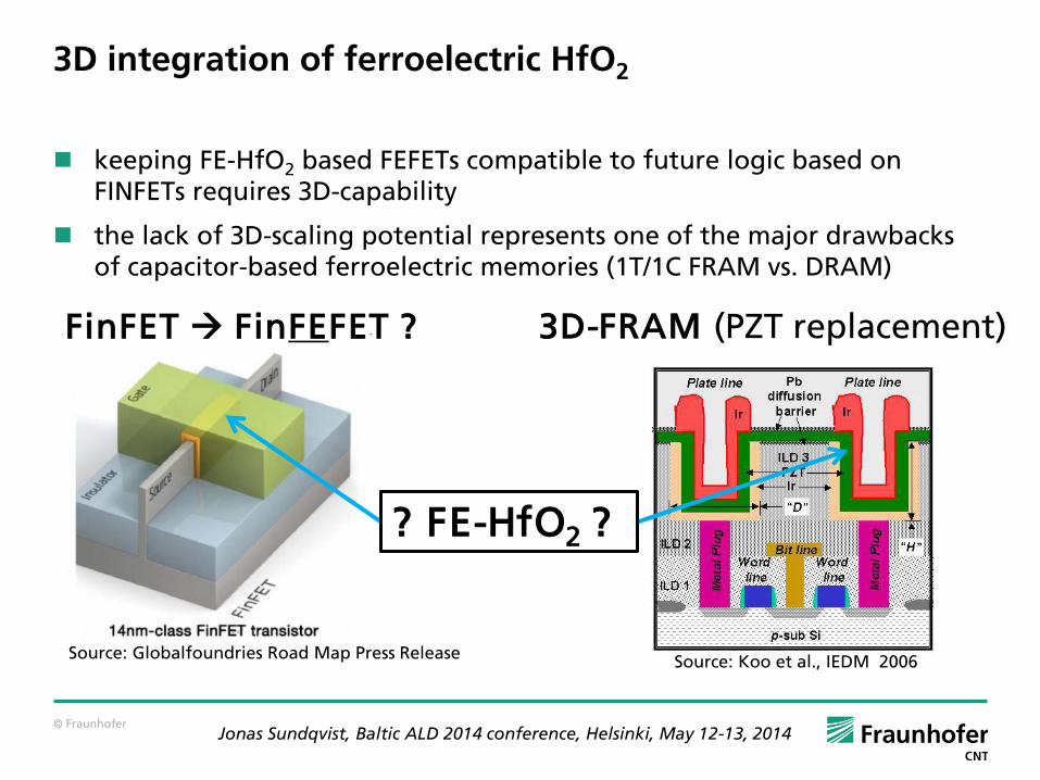
3D integration of ferroelectric HfO2
Source: Globalfoundries Road Map Press Release Source: Koo et al., IEDM 2006
FinFET FinFEFET ? 3D-FRAM (PZT replacement)
? FE-HfO2 ?
keeping FE-HfO2 based FEFETs compatible to future logic based on FINFETs requires 3D-capability
the lack of 3D-scaling potential represents one of the major drawbacks of capacitor-based ferroelectric memories (1T/1C FRAM vs. DRAM)
Jonas Sundqvist, Baltic ALD 2014 conference, Helsinki, May 12-13, 2014
© Fraunhofer
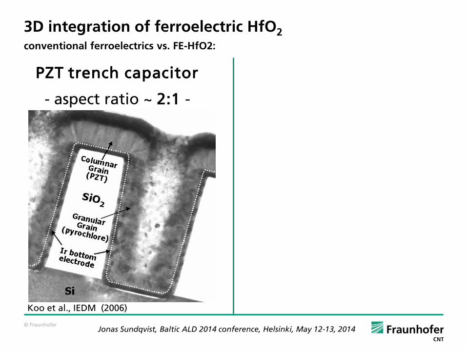
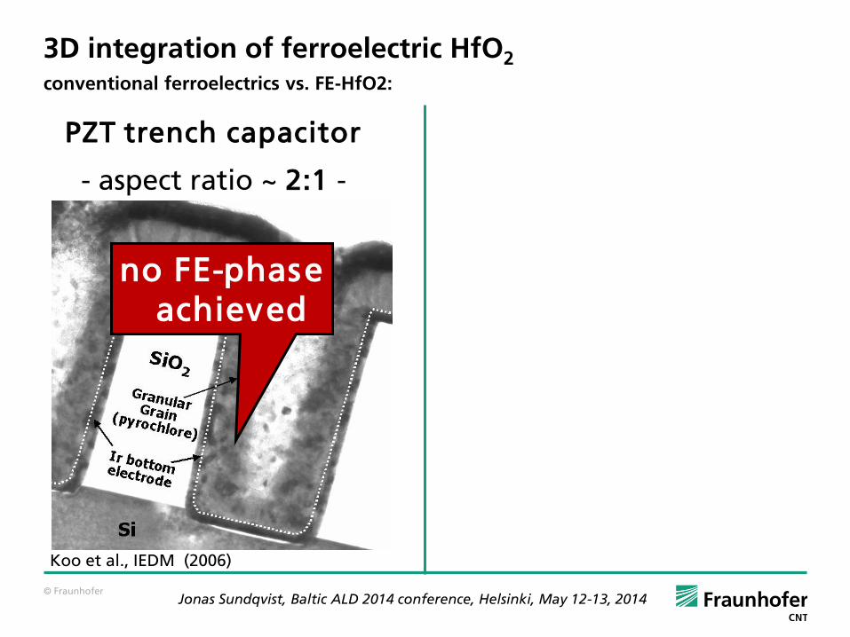
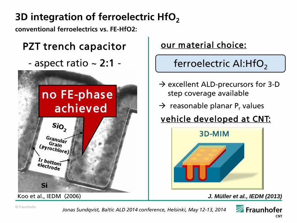
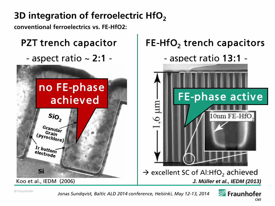
3D integration of ferroelectric HfO2
conventional ferroelectrics vs. FE-HfO2:
Koo et al., IEDM (2006)
PZT trench capacitor
- aspect ratio ~ 2:1 -
Jonas Sundqvist, Baltic ALD 2014 conference, Helsinki, May 12-13, 2014
© Fraunhofer
3D integration of ferroelectric HfO2
conventional ferroelectrics vs. FE-HfO2:
Koo et al., IEDM (2006)
PZT trench capacitor
- aspect ratio ~ 2:1 -
no FE-phase achieved
Jonas Sundqvist, Baltic ALD 2014 conference, Helsinki, May 12-13, 2014
© Fraunhofer
3D integration of ferroelectric HfO2
conventional ferroelectrics vs. FE-HfO2:
Koo et al., IEDM (2006)
PZT trench capacitor
- aspect ratio ~ 2:1 -
no FE-phase achieved
3D-MIM
vehicle developed at CNT:
J. Müller et al., IEDM (2013)
our material choice:
ferroelectric Al:HfO2
excellent ALD-precursors for 3-D step coverage available
reasonable planar Pr values
Jonas Sundqvist, Baltic ALD 2014 conference, Helsinki, May 12-13, 2014
© Fraunhofer
3D integration of ferroelectric HfO2
conventional ferroelectrics vs. FE-HfO2:
Koo et al., IEDM (2006)
PZT trench capacitor
- aspect ratio ~ 2:1 -
no FE-phase achieved
J. Müller et al., IEDM (2013)
FE-HfO2 trench capacitors
- aspect ratio 13:1 -
excellent SC of Al:HfO2 achieved
FE-phase active
Jonas Sundqvist, Baltic ALD 2014 conference, Helsinki, May 12-13, 2014
© Fraunhofer
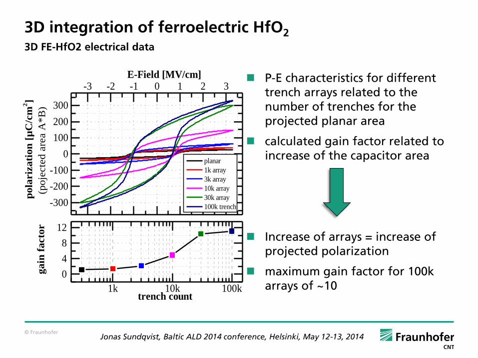
3D integration of ferroelectric HfO2
3D FE-HfO2 electrical data
-3 -2 -1 0 1 2 3
-300
-200
-100
0
100
200
300
E-Field [MV/cm]
planar
1k array
3k array
10k array
30k array
100k trench
pola
riz
ati
on
[µ
C/c
m2]
(poje
cte
d a
rea A
*B
)
1k 10k 100k
0
4
8
12
gain
facto
r
trench count
P-E characteristics for different trench arrays related to the number of trenches for the projected planar area
calculated gain factor related to increase of the capacitor area
Increase of arrays = increase of projected polarization
maximum gain factor for 100k arrays of ~10
Jonas Sundqvist, Baltic ALD 2014 conference, Helsinki, May 12-13, 2014
© Fraunhofer
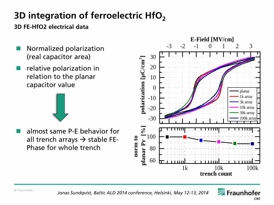
3D integration of ferroelectric HfO2
3D FE-HfO2 electrical data
-3 -2 -1 0 1 2 3
-30
-20
-10
0
10
20
30
E-Field [MV/cm]
planar
1k array
3k array
10k array
30k array
100k array
pola
riz
ati
on
[µ
C/c
m2]
1k 10k 100k
60
80
100n
orm
to
pla
nar P
r
[%]
trench count
Normalized polarization (real capacitor area)
relative polarization in relation to the planar capacitor value
almost same P-E behavior for all trench arrays stable FE-Phase for whole trench
Jonas Sundqvist, Baltic ALD 2014 conference, Helsinki, May 12-13, 2014
© Fraunhofer
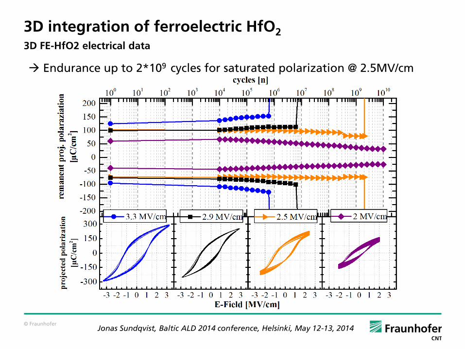
3D integration of ferroelectric HfO2
3D FE-HfO2 electrical data Endurance up to 2*109 cycles for saturated polarization @ 2.5MV/cm
Jonas Sundqvist, Baltic ALD 2014 conference, Helsinki, May 12-13, 2014
© Fraunhofer
3D integration of ferroelectric HfO2
Renewed scaling potential
FE-HfO2 trench capacitor array
minimal Pr penalty for 3D-integration
J. Müller et al., IEDM (2013)
no significant loss of FE-Phase stability observed compared to planar structures
area gain factor completly transfered to gain in polarisation per planar area
-4 -2 0 2 4-400
-200
0
200
400
electric field (MV/cm)
po
lari
zati
on
(µ
C/c
m2)
(pro
ject
ed a
rea A
*B)
2D vs. 3D
x10
A B
3D
A B
2D
Jonas Sundqvist, Baltic ALD 2014 conference, Helsinki, May 12-13, 2014
© Fraunhofer
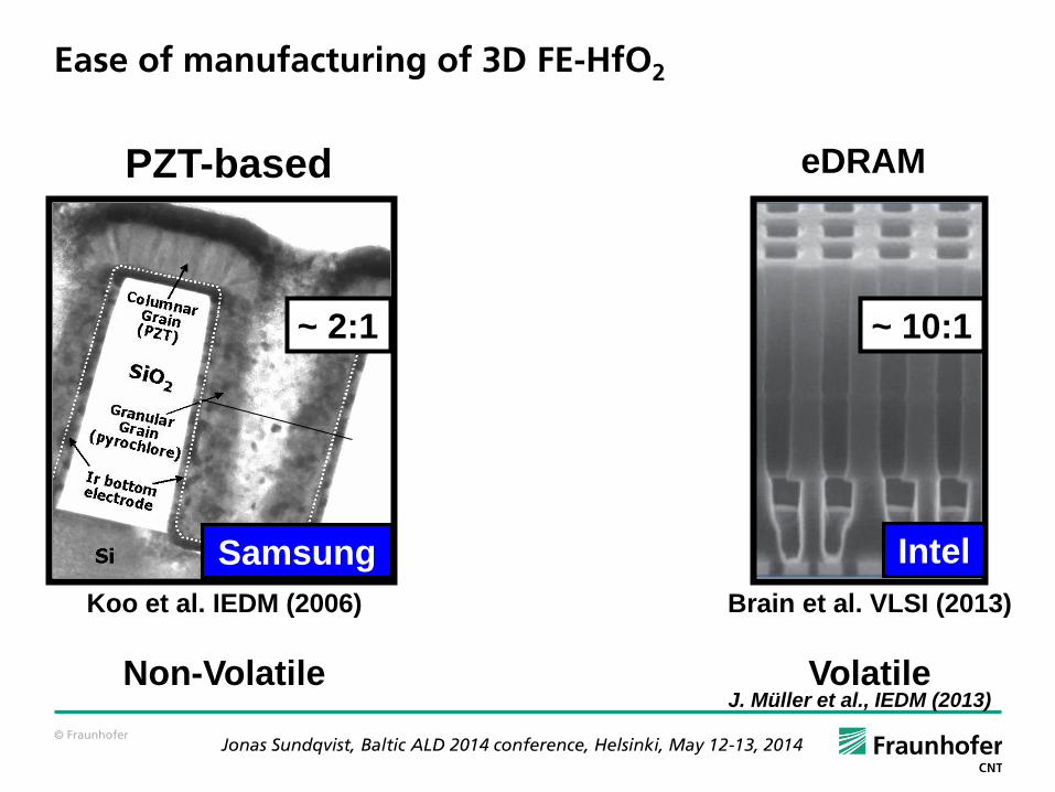
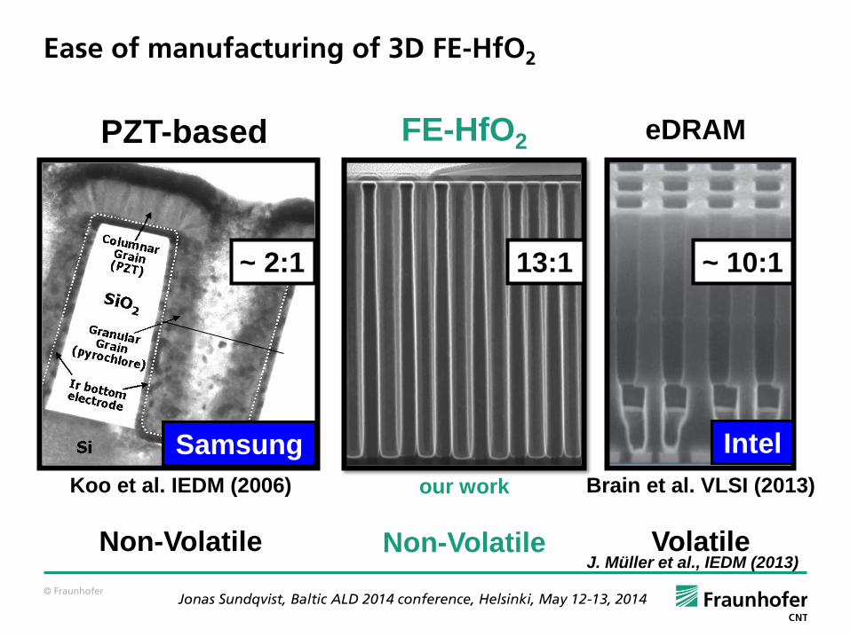
Ease of manufacturing of 3D FE-HfO2
PZT-based eDRAM
~ 10:1 ~ 2:1
Samsung Intel
Koo et al. IEDM (2006)
Non-Volatile
Brain et al. VLSI (2013)
Volatile J. Müller et al., IEDM (2013)
Jonas Sundqvist, Baltic ALD 2014 conference, Helsinki, May 12-13, 2014
© Fraunhofer
Ease of manufacturing of 3D FE-HfO2
PZT-based FE-HfO2 eDRAM
our work
Non-Volatile
~ 10:1 13:1 ~ 2:1
Samsung Intel
Brain et al. VLSI (2013)
Volatile J. Müller et al., IEDM (2013)
Koo et al. IEDM (2006)
Non-Volatile
Jonas Sundqvist, Baltic ALD 2014 conference, Helsinki, May 12-13, 2014
© Fraunhofer
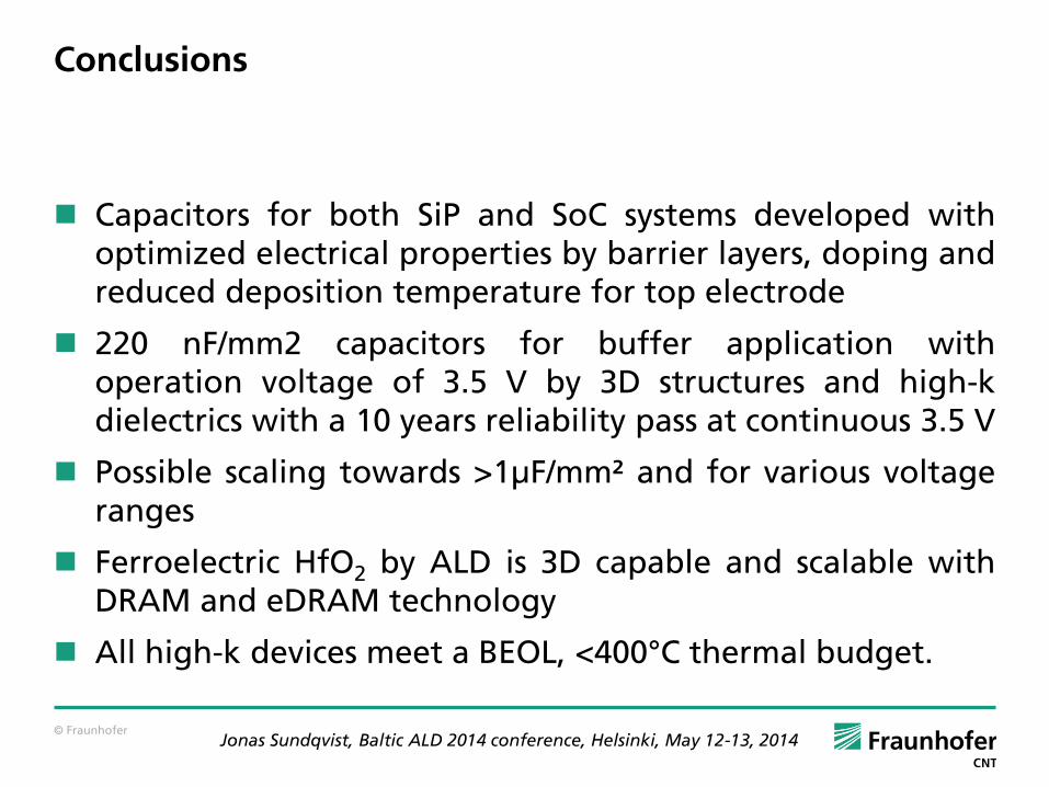
Conclusions
Capacitors for both SiP and SoC systems developed with optimized electrical properties by barrier layers, doping and reduced deposition temperature for top electrode
220 nF/mm2 capacitors for buffer application with operation voltage of 3.5 V by 3D structures and high-k dielectrics with a 10 years reliability pass at continuous 3.5 V
Possible scaling towards >1µF/mm² and for various voltage ranges
Ferroelectric HfO2 by ALD is 3D capable and scalable with DRAM and eDRAM technology
All high-k devices meet a BEOL, <400°C thermal budget.
Jonas Sundqvist, Baltic ALD 2014 conference, Helsinki, May 12-13, 2014
© Fraunhofer high-k Workshop 2014 Jonas Sundqvist
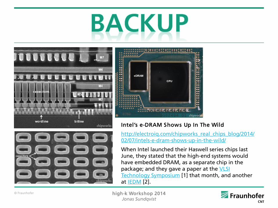
Intel’s e-DRAM Shows Up In The Wild
http://electroiq.com/chipworks_real_chips_blog/2014/02/07/intels-e-dram-shows-up-in-the-wild/
When Intel launched their Haswell series chips last June, they stated that the high-end systems would have embedded DRAM, as a separate chip in the package; and they gave a paper at the VLSI Technology Symposium [1] that month, and another at IEDM [2].

© Fraunhofer
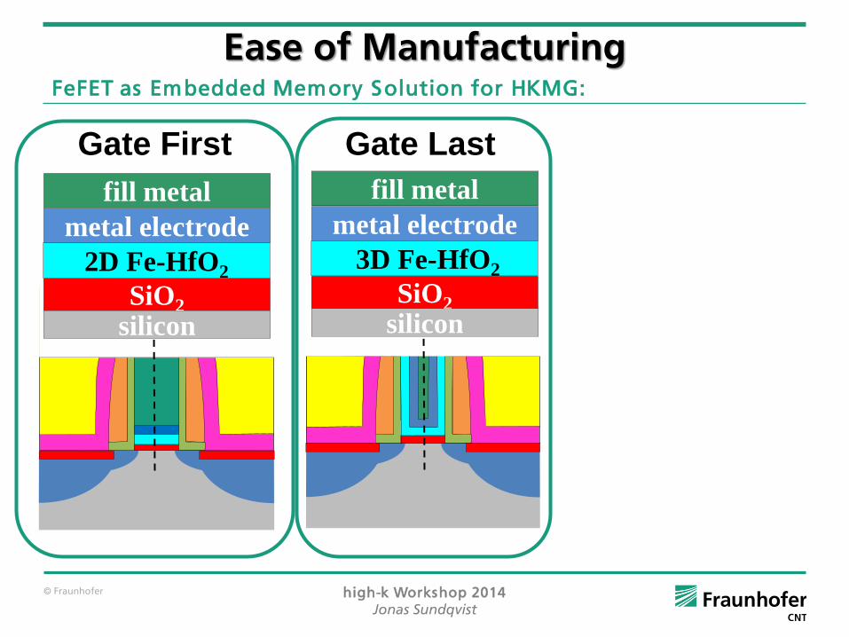
Gate First
Ease of Manufacturing FeFET as Embedded Memory Solution for HKMG:
high-k Workshop 2014 Jonas Sundqvist
SiO2
silicon
2D Fe-HfO2
metal electrode
fill metal
© Fraunhofer
Gate First Gate Last
Ease of Manufacturing FeFET as Embedded Memory Solution for HKMG:
high-k Workshop 2014 Jonas Sundqvist
SiO2
silicon
3D Fe-HfO2
metal electrode
fill metal
SiO2
silicon
2D Fe-HfO2
metal electrode
fill metal
© Fraunhofer
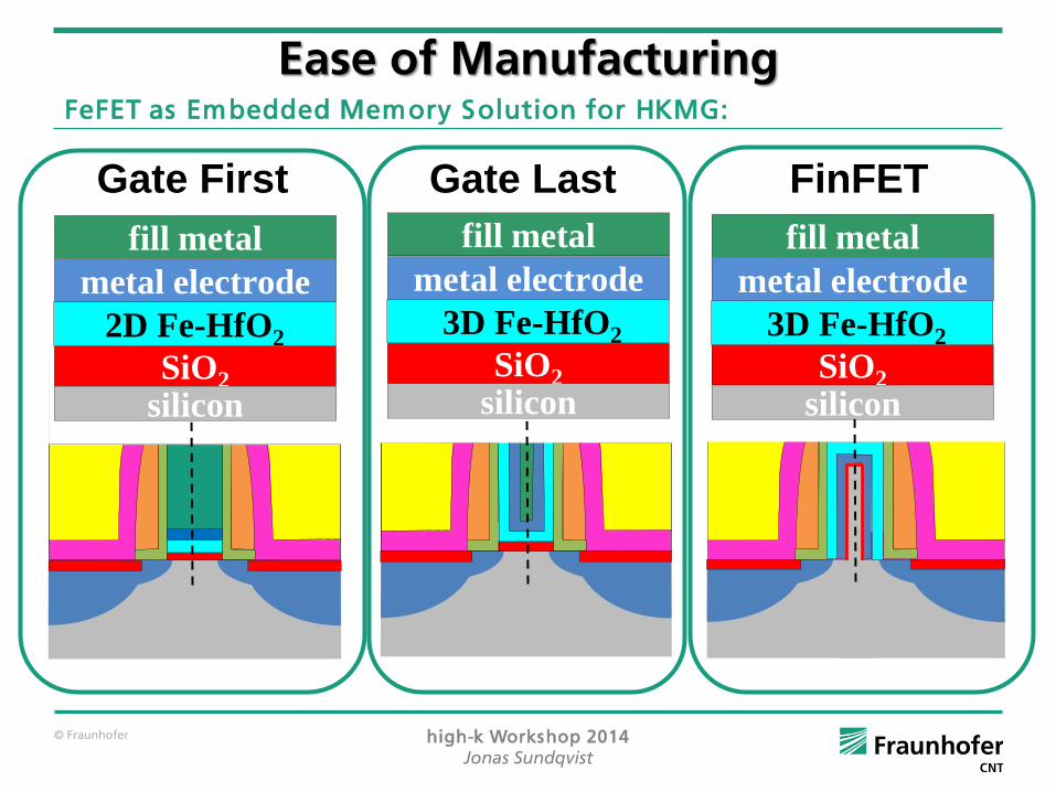
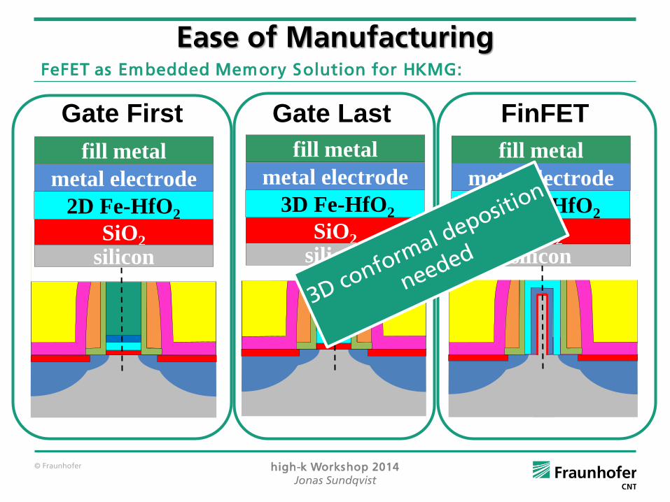
Gate First Gate Last FinFET
Ease of Manufacturing FeFET as Embedded Memory Solution for HKMG:
high-k Workshop 2014 Jonas Sundqvist
SiO2
silicon
3D Fe-HfO2
metal electrode
fill metal
SiO2
silicon
2D Fe-HfO2
metal electrode
fill metal
SiO2
silicon
3D Fe-HfO2
metal electrode
fill metal
© Fraunhofer
Gate First Gate Last FinFET
Ease of Manufacturing FeFET as Embedded Memory Solution for HKMG:
high-k Workshop 2014 Jonas Sundqvist
SiO2
silicon
3D Fe-HfO2
metal electrode
fill metal
SiO2
silicon
2D Fe-HfO2
metal electrode
fill metal
SiO2
silicon
3D Fe-HfO2
metal electrode
fill metal