high quality factor etchless silicon photonic ring resonators quality factor etchless silicon...
TRANSCRIPT
High quality factor etchless silicon photonic ring resonators
Lian-Wee Luo,1,*
Gustavo S. Wiederhecker,1 Jaime Cardenas,
1 Carl Poitras,
1 and
Michal Lipson1,2
1School of Electrical and Computer Engineering, Cornell University, Ithaca, NY 14853, USA 2Kavli Institute at Cornell for Nanoscale Science, Cornell University, Ithaca, NY 14853, USA
Abstract: We demonstrate high quality factor etchless silicon photonic ring resonators fabricated by selective thermal oxidation of silicon without the silicon layer being exposed to any plasma etching throughout the fabrication process. We achieve a high intrinsic quality factor of 510,000 in 50 µm-radius ring resonators, corresponding to a ring loss of 0.8 dB/cm. The device has a total chip insertion loss of 2.5 dB, achieved by designing etchless silicon inverse nanotapers at both the input and output of the chip.
©2011 Optical Society of America
OCIS codes: (230.5750) Resonators; (230.7370) Waveguides.
References and links
1. D. A. B. Miller, “Optical interconnects to silicon,” IEEE J. Sel. Top. Quant. 6(6), 1312–1317 (2000). 2. L. Pavesi, and D. J. Lockwood, Silicon Photonics, Topics in applied physics (Springer, Berlin; New York, 2004),
pp. xvi, 397 p. 3. R. Soref, “The past, present, and future of silicon photonics,” IEEE J. Sel Top. Quant. 12(6), 1678–1687 (2006). 4. M. Haurylau, G. Q. Chen, H. Chen, J. D. Zhang, N. A. Nelson, D. H. Albonesi, E. G. Friedman, and P. M.
Fauchet, “On-chip optical interconnect roadmap: Challenges and critical directions,” IEEE J. Sel. Top. Quant. 12(6), 1699–1705 (2006).
5. F. N. Xia, L. Sekaric, and Y. Vlasov, “Ultracompact optical buffers on a silicon chip,” Nat. Photonics 1(1), 65–71 (2007).
6. Q. F. Xu, P. Dong, and M. Lipson, “Breaking the delay-bandwidth limit in a photonic structure,” Nat. Phys. 3(6), 406–410 (2007).
7. J. Cardenas, M. A. Foster, N. Sherwood-Droz, C. B. Poitras, H. L. R. Lira, B. Zhang, A. L. Gaeta, J. B. Khurgin, P. Morton, and M. Lipson, “Wide-bandwidth continuously tunable optical delay line using silicon microring resonators,” Opt. Express 18(25), 26525–26534 (2010).
8. U. Fischer, T. Zinke, J. R. Kropp, F. Arndt, and K. Petermann, “0.1 dB/cm waveguide losses in single-mode SOI rib waveguides,” IEEE Photon. Tech. L 8(5), 647–648 (1996).
9. S. Lardenois, D. Pascal, L. Vivien, E. Cassan, S. Laval, R. Orobtchouk, M. Heitzmann, N. Bouzaida, and L. Mollard, “Low-loss submicrometer silicon-on-insulator rib waveguides and corner mirrors,” Opt. Lett. 28(13), 1150–1152 (2003).
10. M. A. Webster, R. M. Pafchek, G. Sukumaran, and T. L. Koch, “Low-loss quasi-planar ridge waveguides formed on thin silicon-on-insulator,” Appl. Phys. Lett. 87(23), 231108 (2005).
11. H. S. Rong, A. S. Liu, R. Jones, O. Cohen, D. Hak, R. Nicolaescu, A. Fang, and M. Paniccia, “An all-silicon Raman laser,” Nature 433(7023), 292–294 (2005).
12. P. Dong, W. Qian, S. R. Liao, H. Liang, C. C. Kung, N. N. Feng, R. Shafiiha, J. A. Fong, D. Z. Feng, A. V. Krishnamoorthy, and M. Asghari, “Low loss shallow-ridge silicon waveguides,” Opt. Express 18(14), 14474–14479 (2010).
13. I. Kiyat, A. Aydinli, and N. Dagli, “High-Q silicon-on-insulator optical rib waveguide racetrack resonators,” Opt. Express 13(6), 1900–1905 (2005).
14. L. K. Rowe, M. Elsey, N. G. Tarr, A. P. Knights, and E. Post, “CMOS-compatible optical rib waveguides defined by local oxidation of silicon,” Electron. Lett. 43(7), 392–393 (2007).
15. F. Y. Gardes, G. T. Reed, A. P. Knights, G. Mashanovich, P. E. Jessop, L. Rowe, S. McFaul, D. Bruce, and N. G. Tarr, “Sub-micron optical waveguides for silicon photonics formed via the local oxidation of silicon (LOCOS),” SPIE (2008).
16. R. Pafchek, R. Tummidi, J. Li, M. A. Webster, E. Chen, and T. L. Koch, “Low-loss silicon-on-insulator shallow-ridge TE and TM waveguides formed using thermal oxidation,” Appl. Opt. 48(5), 958–963 (2009).
17. P. Dumon, W. Bogaerts, V. Wiaux, J. Wouters, S. Beckx, J. Van Campenhout, D. Taillaert, B. Luyssaert, P. Bienstman, D. Van Thourhout, and R. Baets, “Low-loss SOI photonic wires and ring resonators fabricated with deep UV lithography,” IEEE Photon. Tech. L 16(5), 1328–1330 (2004).
18. Y. A. Vlasov, and S. J. McNab, “Losses in single-mode silicon-on-insulator strip waveguides and bends,” Opt. Express 12(8), 1622–1631 (2004).
#141283 - $15.00 USD Received 19 Jan 2011; revised 7 Mar 2011; accepted 8 Mar 2011; published 18 Mar 2011(C) 2011 OSA 28 March 2011 / Vol. 19, No. 7 / OPTICS EXPRESS 6284

19. T. Tsuchizawa, K. Yamada, H. Fukuda, T. Watanabe, J. Takahashi, M. Takahashi, T. Shoji, E. Tamechika, S. Itabashi, and H. Morita, “Microphotonics devices based on silicon microfabrication technology,” IEEE J. Sel. Top. Quant. 11(1), 232–240 (2005).
20. J. Niehusmann, A. Vorckel, P. H. Bolivar, T. Wahlbrink, W. Henschel, and H. Kurz, “Ultrahigh-quality-factor silicon-on-insulator microring resonator,” Opt. Lett. 29(24), 2861–2863 (2004).
21. S. J. Xiao, M. H. Khan, H. Shen, and M. H. Qi, “Compact silicon microring resonators with ultra-low propagation loss in the C band,” Opt. Express 15(22), 14467–14475 (2007).
22. G. S. Oehrlein, “Dry Etching Damage of Silicon - a Review,” Mat. Sci. Eng. B. 4(1-4), 441–450 (1989). 23. F. P. Payne, and J. P. R. Lacey, “A Theoretical-Analysis of Scattering Loss from Planar Optical Wave-Guides,”
Opt. Quantum Electron. 26(10), 977–986 (1994). 24. K. K. Lee, D. R. Lim, L. C. Kimerling, J. Shin, and F. Cerrina, “Fabrication of ultralow-loss Si/SiO(2)
waveguides by roughness reduction,” Opt. Lett. 26(23), 1888–1890 (2001). 25. M. Borselli, T. J. Johnson, and O. Painter, “Beyond the Rayleigh scattering limit in high-Q silicon microdisks:
theory and experiment,” Opt. Express 13(5), 1515–1530 (2005). 26. J. Cardenas, C. B. Poitras, J. T. Robinson, K. Preston, L. Chen, and M. Lipson, “Low loss etchless silicon
photonic waveguides,” Opt. Express 17(6), 4752–4757 (2009). 27. Silvaco Athena, retrieved http://www.silvaco.com/products/process_simulation/athena.html. 28. COMSOL 3.5a, Comsol Multiphysics ®, retrieved http://www.comsol.com/. 29. A. Yariv, “Universal relations for coupling of optical power between microresonators and dielectric
waveguides,” Electron. Lett. 36(4), 321–322 (2000). 30. V. R. Almeida, R. R. Panepucci, and M. Lipson, “Nanotaper for compact mode conversion,” Opt. Lett. 28(15),
1302–1304 (2003). 31. P. E. Barclay, K. Srinivasan, and O. Painter, “Nonlinear response of silicon photonic crystal microresonators
excited via an integrated waveguide and fiber taper,” Opt. Express 13(3), 801–820 (2005). 32. P. Rabiei, W. H. Steier, C. Zhang, and L. R. Dalton, “Polymer micro-ring filters and modulators,” J. Lightwave
Technol. 20(11), 1968–1975 (2002).
1. Introduction
Silicon photonics has been studied extensively for on-chip optical interconnects during the past decade as optical interconnects offer a larger bandwidth and lower power consumption in microelectronic chips [1–4]. To realize the goal of optical interconnects in silicon chips, storing or slowing down of optical signals is essential during the routing of the signals. Several on-chip optical buffers based on silicon ring resonators have been demonstrated [5–7]. However, the major challenge faced by these silicon-based optical buffers is the need for low-loss silicon waveguides and high-Q ring resonators.
There are two types of silicon waveguides commonly used by the silicon photonic community, namely rib waveguides and strip waveguides. Rib waveguides with widths of 1-8 μm have exhibited losses down to 0.1 dB/cm but their minimum bending radius is limited to hundreds of micrometers [8–16]. To obtain more compact silicon ring resonators, strip waveguides with dimensions approximately 500 nm wide by 250 nm thick are employed [5–7,17–21]. These strip waveguides have demonstrated intrinsic quality factors up to 400,000 in 10 μm-radius ring resonators with a ring loss not lower than 1.8 dB/cm at λ = 1.53 μm. Here we demonstrate a different type of silicon ring resonators which exhibit lower propagation loss than the strip waveguides and possess smaller bending radius than the rib waveguides.
Losses in silicon waveguides originate largely from the damage of the silicon surfaces by the dry etching processes [22]. The reactive ion etching (RIE) induces surface modifications and results in both the increased scattering losses at the sidewalls due to silicon waveguide roughness and the increased absorption sites at Si/SiO2 interface due to surface residues and lattice damage [23–25]. In order to minimize these losses, we have previously demonstrated an etchless silicon waveguide fabrication process based on selective thermal oxidation of silicon [26]. This etchless silicon waveguide fabrication minimizes the waveguide losses resulting from the dry etching by not exposing the silicon surface to any plasma etching throughout the fabrication process. The etchless silicon waveguides possess the advantages of both the low loss of rib waveguides and the small bending radius of strip waveguides.
In this paper, based on the etchless silicon fabrication, we design and fabricate high-Q etchless silicon photonic ring resonators. We achieve a high intrinsic quality factor of 510,000 in 50 μm-radius ring resonators, corresponding to a ring loss of 0.8 dB/cm. We also design etchless silicon inverse nanotapers to enable efficient coupling from the lensed fiber into the
#141283 - $15.00 USD Received 19 Jan 2011; revised 7 Mar 2011; accepted 8 Mar 2011; published 18 Mar 2011(C) 2011 OSA 28 March 2011 / Vol. 19, No. 7 / OPTICS EXPRESS 6285

chip. The device shows a low coupling loss of approximately 1.5 dB per facet, corresponding to 71% fiber-waveguide coupling efficiency.
2. Etchless silicon photonic ring resonators fabrication process flow
The fabrication of the etchless silicon photonic ring resonator is based on a process of selective thermal oxidation of silicon. The etchless silicon waveguides are fabricated from a silicon-on-insulator (SOI) wafer with an initial silicon layer of 500 nm and a buried oxide layer (BOX) of 3 μm. First we grow a thermal oxide layer of 785 nm on the 500 nm SOI which consumes approximately 360 nm of silicon (see Fig. 1(a)). We then pattern the silicon waveguides with electron beam (e-beam) lithography using ma-N 2405 resist (see Fig. 1(b)). Next we etch the patterned thermally grown oxide layer with a RIE tool using fluorine chemistry, leaving behind a thin 50 nm oxide slab throughout the whole wafer (see Fig. 1(c)). This thin oxide slab protects the silicon surface underneath from the ion bombardment and chemical reactions that occur during the plasma etching. After stripping the e-beam resist, we use wet thermal oxidation to selectively oxidize the silicon (see Fig. 1(d)) and define the silicon waveguides with a thin silicon slab (see Fig. 1(e)). Lastly, the waveguides are clad with 300 nm of high temperature oxide (HTO) to give a highly conformal deposition and 1.8 µm of plasma enhanced chemical vapor deposition (PECVD) silicon dioxide to confine the optical mode completely (see Fig. 1(f)).
Fig. 1. Etchless silicon photonic ring resonator fabrication process flow. (a) Thermal oxidation of a 500 nm silicon-on-insulator (SOI) to leave behind 140 nm thick silicon layer with 785 nm thick thermally grown oxide on top. (b) Patterning of the waveguides using ma-N 2405 resist, leaving a coupling gap between the ring resonator and bus waveguide. (c) Etching of the thermally grown oxide, leaving behind a thin 50 nm oxide slab. (d) Selective wet thermal oxidation of the silicon. (e) Structural profile of the oxidized silicon waveguides. (f) Deposition of 300 nm HTO and 1.8 μm PECVD silicon dioxide.
3. Etchless silicon photonic ring resonators design
The final structural geometry of an etchless silicon photonic device is dependent on the thickness of the thermally grown oxide layer above the silicon, i.e. the thermal oxidation rate of the silicon at the regions with thin oxide slab is faster than that at the regions with thicker oxide layer. The final structural profile of an etchless silicon waveguide has a slowly varying sidewall which is different from the vertical sidewall of an etched silicon waveguide. In
#141283 - $15.00 USD Received 19 Jan 2011; revised 7 Mar 2011; accepted 8 Mar 2011; published 18 Mar 2011(C) 2011 OSA 28 March 2011 / Vol. 19, No. 7 / OPTICS EXPRESS 6286

designing 50 μm-radius etchless silicon photonic ring resonators (see Fig. 2(a)), we use a commercial software Silvaco Athena [27] to simulate the structural profile of the etchless silicon waveguides defined by the selective thermal oxidation process (see Fig. 2(b)). Next we import the simulated profile into Comsol (a finite element modeling software) [28] to compute the modal properties of the etchless silicon waveguides (see Fig. 2(c)). To enable critical coupling at λ = 1.55 μm, the dimensions of the etchless silicon waveguides following the selective thermal oxidation process are designed to be 800 nm wide by 60 nm tall with a coupling gap of 930 nm [29]. The waveguides are fabricated using 800 nm wide by 785 nm thick etched oxide mask and a coupling gap of 930 nm with a wet thermal oxidation time of 20 minutes (see Fig. 1(d)). The scanning electron microscope (SEM) picture in Fig. 2(d) shows the cross-sectional profile of the coupling region and the structural profile of the fabricated device matches with the simulations accurately. This fabrication technique, which avoids any etching of the silicon layer, results in an ultra-smooth top Si/SiO2 interface comparable to the interface between the silicon and the buried oxide, as shown in the transmission electron microscope (TEM) picture of the thin oxidized silicon slab (see Fig. 2(e)).
Fig. 2. (a) SEM picture of the fabricated 50 µm-radius etchless silicon photonic ring resonator. (b) Simulated structural profiles of the etchless silicon ring resonator with coupling gap = 930 nm. (c) Symmetric mode of the bus waveguide and the ring resonator. (d) Cross-sectional SEM picture of the coupling region. (e) Transmission electron microscope (TEM) picture of the thin oxidized silicon slab.
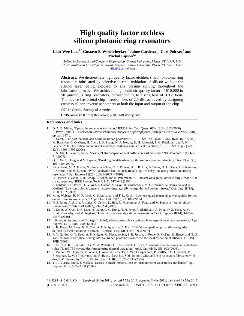
The 800 nm wide etchless silicon waveguide forming the ring resonator supports only one mode, i.e. the fundamental TE mode (see Fig. 3(a)). The advantage of supporting only the fundamental TE mode is that the polarization mode conversion is minimized, thus reducing the crosstalk in polarization. The 800 nm waveguide has an effective index of 1.6 at λ = 1.55 μm and a mode size of 1 μm wide by 0.52 μm high. On the other hand, a lensed fiber has an effective index of 1.468 and a mode field diameter of 2.5 μm. The coupling of light directly from the lensed fiber into the 800 nm waveguide results in a measured coupling loss of more than 10 dB. This coupling loss is high due to both the refractive index mismatch and mode mismatch between the lensed fiber and the etchless silicon waveguide. To minimize the coupling loss, a 220 nm wide etchless silicon inverse nanotaper with a taper length of 100 μm is integrated at both the input waveguide and output waveguide [30]. The designed inverse nanotaper has an effective index of 1.453 and a mode size of 5 µm wide by 2 µm high (see Fig. 3(b)). Due to this improved match in refractive index and mode size, the coupling loss
#141283 - $15.00 USD Received 19 Jan 2011; revised 7 Mar 2011; accepted 8 Mar 2011; published 18 Mar 2011(C) 2011 OSA 28 March 2011 / Vol. 19, No. 7 / OPTICS EXPRESS 6287
from the lensed fiber into the inverse nanotaper is reduced to approximately 1.5 dB. This measured coupling loss is one of the lowest demonstrated in silicon photonic devices.
Fig. 3. Transverse electric (TE) mode profile (Ex-component) of (a) Etchless silicon waveguide. (b) Etchless silicon inverse nanotaper.
4. Results and discussions
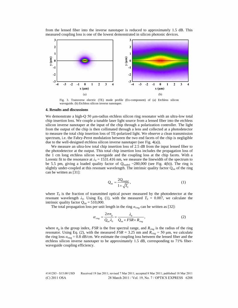
We demonstrate a high-Q 50 μm-radius etchless silicon ring resonator with an ultra-low total chip insertion loss. We couple a tunable laser light source from a lensed fiber into the etchless silicon inverse nanotaper at the input of the chip through a polarization controller. The light from the output of the chip is then collimated through a lens and collected at a photodetector to measure the total chip insertion loss of TE-polarized light. We observe a clean transmission spectrum, i.e. the Fabry-Perot modulation between the two end facets of the chip is negligible due to the well-designed etchless silicon inverse nanotaper (see Fig. 4(a)).
We measure an ultra-low total chip insertion loss of 2.5 dB from the input lensed fiber to the photodetector at the output. This total chip insertion loss includes the propagation loss of the 1 cm long etchless silicon waveguide and the coupling loss at the chip facets. With a Lorentz fit to the resonance at λ0 = 1531.416 nm, we measure the linewidth of the spectrum to be 5.5 pm, giving a loaded quality factor of Qloaded ~280,000 (see Fig. 4(b)). The ring is slightly under-coupled at this resonant wavelength. The intrinsic quality factor Qint of the ring can be written as [31]:
int
0
2,
1
loadedQQ
T
(1)
where T0 is the fraction of transmitted optical power measured by the photodetector at the resonant wavelength λ0. Using Eq. (1), with the measured T0 = 0.007, we calculate the intrinsic quality factor Qint = 510,000.
The total propagation loss per unit length in the ring αring can be written as [32]:
0
int 0 int
2,
g
ring
ring
n
Q Q FSR R
(2)
where ng is the group index, FSR is the free spectral range, and Rring is the radius of the ring resonator. Using Eq. (2), with the measured FSR = 3.25 nm and Rring = 50 μm, we calculate the ring loss αring = 0.8 dB/cm. We estimate the coupling loss between the lensed fiber and the etchless silicon inverse nanotaper to be approximately 1.5 dB, corresponding to 71% fiber-waveguide coupling efficiency.
#141283 - $15.00 USD Received 19 Jan 2011; revised 7 Mar 2011; accepted 8 Mar 2011; published 18 Mar 2011(C) 2011 OSA 28 March 2011 / Vol. 19, No. 7 / OPTICS EXPRESS 6288
Fig. 4. (a) Through-port transmission spectrum of the ring resonator in transverse electric (TE) polarization. (b) Normalized transmission spectrum at λ0 = 1531.416 nm.
5. Conclusion
We designed and fabricated high-Q etchless silicon photonic ring resonators using selective thermal oxidation of silicon without the silicon layer being exposed to any plasma etching throughout the fabrication process. We achieved a high intrinsic quality factor of 510,000 in 50 µm-radius ring resonators, corresponding to a ring loss of 0.8 dB/cm. We also realized an ultra-low total chip insertion loss of 2.5 dB with a fiber-waveguide coupling loss of approximately 1.5 dB by employing etchless silicon inverse nanotapers at both the input and output of the device chip. The low loss etchless silicon photonic ring resonators have promising applications in silicon ring resonators-based optical buffers.
Acknowledgments
The authors acknowledge use of the facilities at the Cornell Center for Materials Research, which is supported by the NSF (award number NSF DMR-0520404), and thank Malcolm Thomas and John Grazul for assistance in operating the focused ion beam and transmission electron microscope. This work was partially funded under the DARPA MTO Si-PhASER project Grant HR0011-09-0013 with the University of California, Davis, and under Grant FA9550-05-1-0414 with Stanford University. This work was performed in part at the Cornell Nanoscale Facility, a member of the National Nanotechnology Infrastructure Network, which is supported by the NSF. Lian-Wee Luo acknowledges a fellowship from Agency of Science, Technology and Research (A*STAR), Singapore.
#141283 - $15.00 USD Received 19 Jan 2011; revised 7 Mar 2011; accepted 8 Mar 2011; published 18 Mar 2011(C) 2011 OSA 28 March 2011 / Vol. 19, No. 7 / OPTICS EXPRESS 6289