high-speed link modeling: analog/digital equalization and...
TRANSCRIPT

HIGH-SPEED LINK MODELING:
ANALOG/DIGITAL EQUALIZATION AND MODULATION TECHNIQUES
A Thesis
by
KEYTAEK LEE
Submitted to the Office of Graduate Studies of Texas A&M University
in partial fulfillment of the requirements for the degree of
MASTER OF SCIENCE
May 2012
Major Subject: Electrical Engineering

HIGH-SPEED LINK MODELING:
ANALOG/DIGITAL EQUALIZATION AND MODULATION TECHNIQUES
A Thesis
by
KEYTAEK LEE
Submitted to the Office of Graduate Studies of Texas A&M University
in partial fulfillment of the requirements for the degree of
MASTER OF SCIENCE
Approved by:
Chair of Committee, Samuel Palermo Committee Members, Jose Silva-Martinez Krishna R. Narayanan Duncan M. Walker Head of Department, Costas Georghiades
May 2012
Major Subject: Electrical Engineering

iii
ABSTRACT
High-speed Link Modeling: Analog/Digital Equalization and Modulation Techniques.
(May 2012)
Keytaek Lee, B.E., State University of New York at Stony Brook
Chair of Advisory Committee: Dr. Samuel Palermo
High-speed serial input-output (I/O) link has required advanced equalization and
modulation techniques to mitigate inter-symbol interference (ISI) caused by multi-Gb/s
signaling over band-limited channels. Increasing demands for transceiver power and area
complexity has leveraged on-going interest in analog-to-digital converter (ADC) based
link, which allows for robust equalization and flexible adaptation to advanced signaling.
With diverse options in ISI control techniques, link performance analysis for
complicated transceiver architectures is very important. This work presents advanced
statistical modeling for ADC-based link, performance comparison of existing
modulation and equalization techniques, and proposed hybrid ADC-based receiver that
achieves further power saving in digital equalization.
Statistical analysis precisely estimates high-speed link margins at given
implementation constrains and low target bit-error-rate (BER), typically ranges from 1e-
12 to 1e-15, by applying proper statistical bound of noise and distortion. The proposed
statistical ADC-based link modeling utilizes bounded probability density function (PDF)
of limited quantization distortion (4-6 bits) through digital feed-forward and decision

iv
feedback equalizers (FFE-DFE) to improve low target BER estimation. Based on
statistical modeling, this work surveys the impact of insufficient equalization, jitter and
crosstalk on modulation selection among two and four level pulse amplitude modulation
(PAM-2 and PAM-4, respectively) and duobinary, and ADC resolution reduction
performance by partial analog equalizer (PAE).
While the information of channel loss at effective Nyquist frequency and
signaling constellation loss initially guides modulation selection, the statistical analysis
results show that PAM-4 best tolerates jitter and crosstalk, and duobinary requires the
least equalization complexity. Meanwhile, despite robust digital equalization, high-speed
ADC complexity and power consumption is still a critical bottleneck, so that PAE is
necessitated to reduce ADC resolution requirement. Statistical analysis presents up to 8-
bit resolution is required in 12.5Gb/s data communications at 46dB of channel loss
without PAE, while 5-bit ADC is enough with 3-tap FFE PAE. For optimal ADC
resolution reduction by PAE, digital equalizer complexity also increases to provide
enough margin tolerating significant quantization distortion. The proposed hybrid
receiver defines unreliable signal thresholds by statistical analysis and selectively takes
additional digital equalization to save potentially increasing dynamic power
consumption in digital. Simulation results report that the hybrid receiver saves at least 64%
of digital equalization power with 3-tap FFE PAE in 12.5Gb/s data rate and up to 46dB
loss channels. Finally, this work shows the use of embedded-DFE ADC in the hybrid
receiver is limited by error propagation.

v
DEDICATION
To my wife and two sons,
for giving me the reason and hope of my life
To my parents and parents in laws,
for their love and support

vi
ACKNOWLEDGEMENTS
I would first and foremost like to thank my advisor, Dr. Samuel Palermo, for his
teaching, guiding, motivating, encouraging and supporting throughout my graduate
studies. His excellence in research and supervision has not only nurtured my research
capability but also trained metal strength and way of thinking. I would like to thank all
my committee members, Dr. Jose Silva-Martinez, Dr. Krishna Narayanan, Dr. Duncan
Walker and also Dr. Rabi Mahapatra who served as a substitute committee member for
my defense, for their concerns, time and valuable suggestions. I thank Ehsan Zhian
Tabasy and Ayman Shafik for great experiences of co-work, helps, and valuable
discussions. I thank Jusung Kim for his advices related to research and studies. I also
thank all my friends, Won Suk Lee, Kyu Ha Choe, Kun Mo Kim, Harish
Krishnamoorthy, and Hao Huang for learning and discussing together in valued course
works.

vii
TABLE OF CONTENTS
Page
ABSTRACT .......................................................................................................... iii
DEDICATION....................................................................................................... v
ACKNOWLEDGEMENTS ................................................................................... vi
TABLE OF CONTENTS ....................................................................................... vii
LIST OF FIGURES ............................................................................................... ix
LIST OF TABLES ................................................................................................. xii
CHAPTER
I INTRODUCTION ................................................................................ 1
1.1 Organization of Thesis ................................................................... 3
II STATISTICAL LINK MODELING ...................................................... 5
2.1 Binary Link Modeling .................................................................... 5 2.1.1 Channel Modeling ............................................................ 6 2.1.2 Equalization and Modulation Modeling ............................ 12 2.1.3 Jitter Modeling .................................................................. 15 2.2 Analog-to-Digital Converter (ADC) Based Link Modeling ............. 19
III MODULATION TECHNIQUES AND ANALYSIS ............................. 26
3.1 Initial Guidance for Modulation Selection ...................................... 26 3.2 Advanced Modulation Selection ..................................................... 28
IV EQUALIZATION TECHNIQUES AND ANALYSIS ........................... 36
4.1 Linear Partial Analog Equalizer (PAE) ............................................ 36 4.2 Hybrid Architecture ........................................................................ 46 4.3 Decision Feedback Equalizer (DFE) for Partial Equalization .......... 51

viii
CHAPTER Page
V CONCLUSION AND FUTURE WORK ................................................ 57
5.1 Future Work .................................................................................... 58
REFERENCES ...................................................................................................... 61
VITA ..................................................................................................................... 66

ix
LIST OF FIGURES
FIGURE Page
1 (a) Binary link with multi-tap DFE and (b) ADC-based link .................... 2 2 Electrical backplane channel.................................................................... 6 3 Channel and crosstalk frequency responses ............................................. 7 4 (a) Channel pulse response and its sampled response and (b) {101} pattern pulse response and its sampled response at 10Gb/s in the thru channel in Fig. 3. ..................................................................................... 8 5 Crosstalk channel pulse response and its sampled response at 10Gb/s in the thru channel in Fig. 3. .................................................................... 8 6 Procedure to create ISI + random noise CDF and estimate statistical eye opening with PAM-2 signaling and 1e-12 of the target BER .................... 10 7 Comparison between CDFs by statistical modeling and approximated normal distribution .................................................................................. 11 8 Equalized pulse response by 3-tap FFE and 1-tap DFE ........................... 12 9 ((a) Through and crosstalk channel frequency responses [18] and (b) statistical eye degradation by 2%UI DJ and 2%UIrms RJ of RX jitter ..... 16 10 Procedure of RX jitter modeling and comparison between statistical eye contour referred to 1e-12 of BER and 1k-bit transient simulation eye diagram ............................................................................................. 17 11 (a) TX impulse jitter model and (b) jitter sensitivity function (JSF) at the channel output ......................................................................................... 18 12 Procedure for duty cycle TX jitter modeling ........................................... 19 13 (a) Quantization distortion in digital FFE-DFE, (b) proposed statistical modeling for ADC-based receiver with digital FFE-DFE, and (c) comparing statistical modeling with Gaussian-approximated quantization distortion ............................................................................. 21

x
FIGURE Page
14 Channel frequency responses [18] .......................................................... 23 15 Bathtub curve comparison at channel 1 in Fig. 14 (a) with 8-bit ADC, (b) 6-bit ADC, (c) 5-bit ADC, and (d) 4-bit ADC .................................... 24 16 Bathtub curve comparison at channel 2 in Fig. 14 (a) with 8-bit ADC, (b) 6-bit ADC, (c) 5-bit ADC, and (d) 4-bit ADC .................................... 25 17 Through and crosstalk channels [18] in (a) case 2 and (b) case 3.............. 27 18 Pre and post equalized channel frequency responses by 3-tap FFE with PAM-2, PAM-4 and duobinary ........................................................ 31 19 Maximum achievable data rate with different number of FFE taps ........... 32 20 Eye degradation by increasing RX random jitter sigma in case 3 ............. 33 21 Crosstalk channel frequency responses filtered by 3-tap FFE in case 3 .... 33 22 Eye degradation by increasing crosstalk in case 3 .................................... 35 23 Modulation selection range changes due to limited equalization, jitter and crosstalk ............................................................................................ 35 24 1k-bits 10Gb/s PAM-2 eye diagram with (a) channel only, (b) channel + 2-tap FFE, and (c) channel + cascaded 2-tap and 6-tap FFE at a channel with -35.1dB loss @5GHz.................................................... 37 25 2-tap TX CML FFE ................................................................................. 38 26 Simplified 2-tap RX SFFE with time-interleaved ADC............................ 39 27 Group 1: channel frequency responses without reflection [18] ................ 40 28 Group 2: channel frequency responses with reflection [18] ..................... 41 29 10Gb/s minimum ADC resolution requirement without PAE ................... 42 30 10Gb/s minimum ADC resolution requirement with 2-tap FFE PAE ....... 43
xi
FIGURE Page
31 10Gb/s minimum ADC resolution requirement with 3-tap FFE PAE ....... 43 32 12.5Gb/s minimum ADC resolution requirement with 6/1-tap digital FFE/DFE and No/2/3-tap FFE PAE at channel 6-11 in group 1 ............... 45 33 12.5Gb/s minimum ADC resolution requirement with 12/2-tap digital FFE/DFE and No/2/3-tap FFE PAE at channel 1-3 in group 2 ................. 45 34 Statistical bathtub curves (a) with open-eye and (b) with closed-eye ....... 47 35 Proposed hybrid architecture .................................................................. 48 36 10Gb/s digital equalization power saving efficiency with No/2/3-tap FFE PAE......................................................................................................... 49 37 12.5Gb/s digital equalization power saving efficiency with 2/3-tap FFE PAE......................................................................................................... 50 38 Modified hybrid architecture for embedded-DFE .................................... 52 39 12.5Gb/s digital equalization power saving efficiency with 2/3-tap FFE and 1-tap ideal DFE PAE ........................................................................ 53 40 12.5Gb/s 1G-bit transient CDF at reflective channel 3 with and without 1-tap DFE ................................................................................................ 54 41 (a) Transient simulation PDF and (b) its CDF and tail extrapolation with 10Gb/s data rate and 1-tap DFE at channel 3 in Fig. 27 ............................ 55 42 Power efficiency improvement by 1-tap DFE ......................................... 56

xii
LIST OF TABLES
TABLE Page I Channel loss profiles .............................................................................. 28 II Modulation gain ..................................................................................... 28 III Simulation setting for the three cases in Table I ...................................... 29 IV Case 1: FFE coefficients and statistical eye opening ............................... 30 V Case 2: FFE coefficients and statistical eye opening ............................... 30 VI Case 3: FFE coefficients and statistical eye opening ............................... 30 VII Modulation gain by statistical analysis ..................................................... 31 IX Simulation settings for ADC resolution requirement ............................... 42

1
CHAPTER I
INTRODUCTION
As the data rate of high-speed input/output (I/O) links exceeds multi-Gb/s,
undesirable interferences from neighbor transmitting symbols and adjacent signal paths
in electrical channel significantly hinder successful wired communications [1]. With
rapidly enhancing transceiver capability with CMOS scaling, equalization techniques are
required to mitigate inter-symbol interference (ISI) arising from signaling over band-
limited channels. Meanwhile, high-density I/O applications have area and power
restrictions, which limits complexity of transceiver architectures. This restriction
obscures fully analog equalization due to resolution limitation [2] and difficulties to
implement integrated analog delay cells [3]. Although a conventional binary receiver
with multi-tap decision-feedback equalizer (DFE) helps further increasing achievable
data rate (Fig. 1(a)) [4]-[6], analog blocks face harsher challenges due to process,
voltage and temperature (PVT) variation. Besides, DFE itself is restricted to cancel post
cursor ISI and less efficient for long tail ISI.
Increasing demands for advanced equalization and modulation techniques have
led on-going interest in ADC-based high-speed links (Fig.1(b)) that leverage digital
signal processing (DSP), which provides 1) robustness and adaptability in equalization, 2)
flexibility for potential modulation schemes, 3) endurableness for PVT variations, and 4)
scalability with CMOS technology improvement [7]-[11]. Despite the advantages of
____________ This thesis follows the style of IEEE Transactions on Circuits and Systems.

2
(a)
(b)
Fig. 1 (a) Binary link with multi-tap DFE and (b) ADC-based link
DSP, the most critical bottleneck in ADC-based receivers is high-speed ADC’s power
and area consumption, which limits typical ADC resolution to 4-6 bits. With limited
resolution of ADC, quantization distortion is significantly issued in digital equalization.
To relax ADC resolution requirement, a partial analog equalizer (PAE) and full-scale
range (FSR) adjustment are necessitated [7], [12].
Rising complexity of ADC-based receivers with various equalization and
modulation techniques motivates elaborate link modeling to quickly and trustfully
survey the optimal combinations in diverse options. Statistical link modeling has been
considered as one of the best approaches in link performance analysis because of its
acceptable computational complexity and reliability. While statistical modeling for fully
analog high-speed links has grown mature [13]-[15], link modeling approaches for
ADC-based receivers and digital equalizers, often use ADC performance metrics based

3
on mean-square error (MSE), such as signal-to-noise and distortion ratio (SNDR) or
effective number of bits (ENOB) [9], [10], [12], [16]. To simplify analysis, ADC
quantization distortion is often approximated as a normal distribution, and the total error
variance is assumed to be the sum of the random noise and quantization distortion
variance. While this is valid when random noise dominates over quantization distortion,
this is not the case for low-resolution high-speed link systems.
The objectives of this thesis are to build statistical model for ADC-based link
with limited quantization levels, explore performances and tradeoffs of existing solutions
in modulation and equalization techniques for high-speed transceivers by statistical
analysis, and propose a hybrid receiver which improves power efficiency of ADC-based
links.
1.1 Organization of Thesis
Chapter 2 presents an overview of statistical binary link modeling including
band-limited channel, analog equalization, controlled signaling and non-ideal TX/RX
timing. To extend previous statistical analysis for ADC-based link, statistical modeling
for significant amount of quantization distortion by limited resolution ADC with
following digital FFE-DFE is proposed.
Chapter 3 introduces an initial guidance in modulation selection among binary
signaling (PAM-2), four-level pulse-amplitude-modulation (PAM-4) and duobinary in
previous work and reviews the impacts of non-sufficient equalization, crosstalk and jitter
on advance modulation selection by statistical analysis.

4
In Chapter 4, ADC resolution requirement reduction performed by PAE is
reexamined by statistical modeling. Then, the new hybrid architecture which allows for
additional saving of digital equalization power by the selective equalization technique is
proposed. In addition, potential uses and drawbacks of embedded-DFE ADC is
discussed.
Finally, Chapter 5 concludes the thesis with performance comparison for
different modulation and equalization techniques and presents expected research
extensions beyond this work.
5
CHAPTER II
STATISTICAL LINK MODELING
Statistical link modeling captures statistical natures of disturbances such as ISI,
crosstalk, jitter and random noise, and estimates bit-error-rate (BER) in probability
density function (PDF) domain. This better performs for fast and accurate link
performance estimation with extremely low target BER, typically ranging from 1e-12 to
1e-15, than the other approaches; transient simulation requires demanding tasks; worst
case analysis is highly pessimistic [13]; mean-square-error (MSE) based analysis is
based on Gaussian approximation for overall noise and distortion which is often invalid
BER estimation for low target BER due to unbounded tail probability of a normal
distribution [14]. This chapter summarizes statistical binary link modeling techniques in
previous works and extends it for ADC-based link modeling.
2.1 Binary Link Modeling
Binary link consists of a channel, transmitter (TX), receiver (RX), analog
equalizer, and timing circuits such as TX phase locked loop (PLL) and RX clock data
recovery (CDR). This section presents an overview of statistical binary link modeling
including the listed link components.

6
2.1.1 Channel Modeling
Fig. 2 Electrical backplane channel
Over a multi-Gb/s wired communications through electrical channels face three
main disturbances causing signal interferences, which are dispersion, reflection and
crosstalk [1]. Fig. 2 describes an electrical backplane channel components and sources of
interferences. At first, dispersion occurs by limited high frequency current density at
conductor surfaces (skin effect) and signal energy absorption into quickly rotating
dielectric atoms along with alternating electric field due to high frequency signal
(dielectric absorption). Secondly, discontinuity at vias and mismatch at on-chip
termination reflect a part of transmitting signal, which affects on following signals.
Thirdly, high frequency signal is leaked into neighbor channels through parasitics
between densely placed and coupled wires. As a result, a high-speed data
communication over an electrical channel suffers from band limitation due to dispersion,
undesirable high frequency boosting due to reflections, and interferers from neighbor
channels called crosstalk. A physical channel is often assumed as linear and time-

7
invariant (LTI) system and measured as a form of s-parameter, which stands for a ratio
between input and output signals at different ports [17]. For instance, S21 in a two-port
network presents the amount of output signal versus the input through the channel, while
S11 shows the input reflection coefficient at given frequency components. Fig. 3 shows
examples of the observed channel frequency responses of a communicating and crosstalk
channels [18]. In addition to ISI and crosstalk, there exists another source increasing a
chance of error, random noise. This is mainly caused by PVT variation and potential
mismatches both in channel and TX/RX driver. Random noise is typically considered as
an additive white Gaussian noise (AWGN) with zero mean and receiver’s input referred
sigma (standard deviation).
Fig. 3 Channel and crosstalk frequency responses [18]
Based on LTI assumption, a received pulse passed through a channel is obtained
by convolving a unit pulse with channel impulse response which is inverse Fourier
transform of the channel frequency response [19]. Channel pulse response in Fig. 4(a)

8
clearly shows how adjacent symbols interfere with each other. Given ‘101’ of the
transmitting data pattern, parts of pre and post ‘1’ symbols appears at ‘0’ symbol
reception and causes an error as shown in Fig. 4(b). Moreover, sampled values from
adjacent crosstalk channel (Fig. 5) and random noise disturb transmitted symbol
detection.
(a) (b)
Fig. 4 (a) Channel pulse response and its sampled response and (b) {101} pattern pulse
response and its sampled response at 10Gb/s in the thru channel in Fig. 3.
Fig. 5 Crosstalk channel pulse response and its sampled response at 10Gb/s in the thru channel in Fig. 3.
9
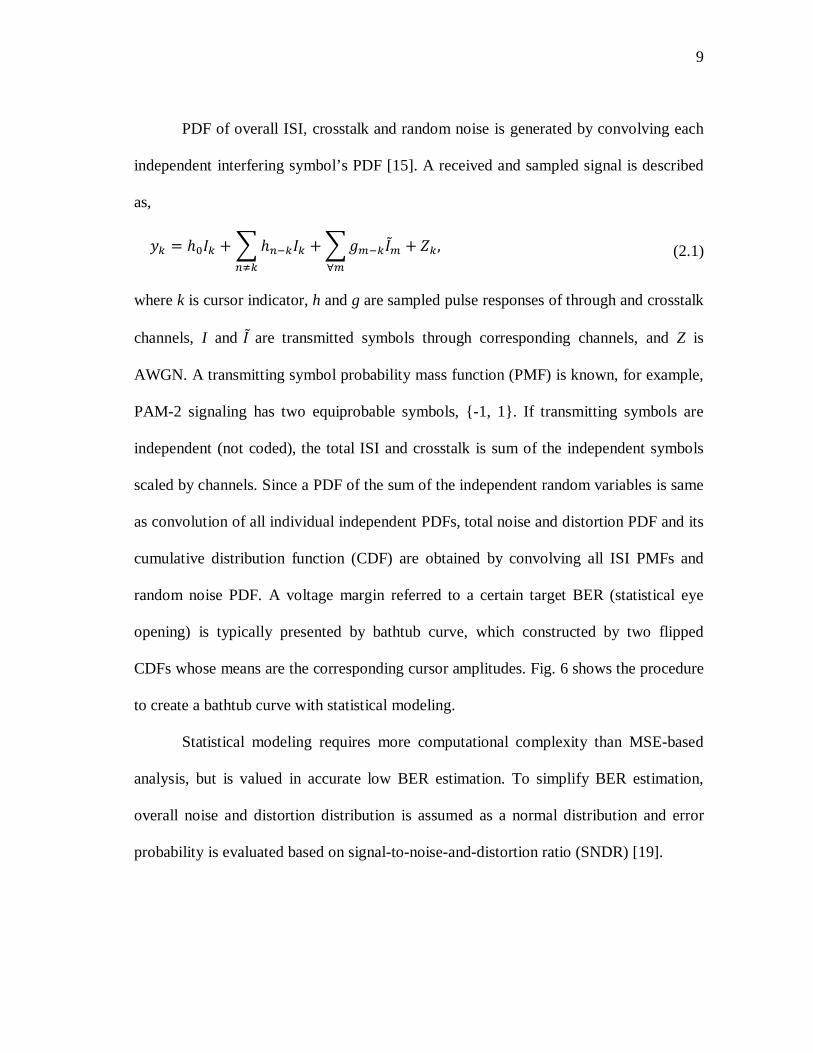
PDF of overall ISI, crosstalk and random noise is generated by convolving each
independent interfering symbol’s PDF [15]. A received and sampled signal is described
as,
𝑦𝑘 = ℎ0𝐼𝑘 + �ℎ𝑛−𝑘𝐼𝑘𝑛≠𝑘
+ �𝑔𝑚−𝑘𝐼𝑚 + 𝑍𝑘∀𝑚
, (2.1)
where k is cursor indicator, h and g are sampled pulse responses of through and crosstalk
channels, I and 𝐼 are transmitted symbols through corresponding channels, and Z is
AWGN. A transmitting symbol probability mass function (PMF) is known, for example,
PAM-2 signaling has two equiprobable symbols, {-1, 1}. If transmitting symbols are
independent (not coded), the total ISI and crosstalk is sum of the independent symbols
scaled by channels. Since a PDF of the sum of the independent random variables is same
as convolution of all individual independent PDFs, total noise and distortion PDF and its
cumulative distribution function (CDF) are obtained by convolving all ISI PMFs and
random noise PDF. A voltage margin referred to a certain target BER (statistical eye
opening) is typically presented by bathtub curve, which constructed by two flipped
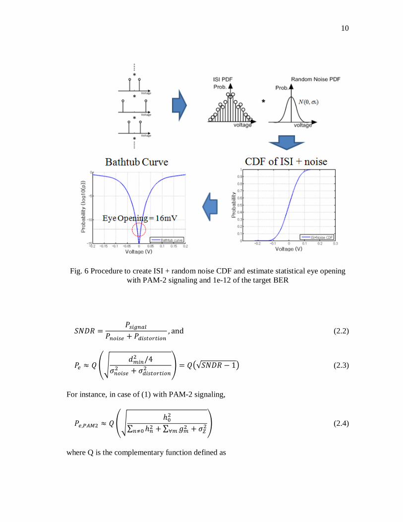
CDFs whose means are the corresponding cursor amplitudes. Fig. 6 shows the procedure
to create a bathtub curve with statistical modeling.
Statistical modeling requires more computational complexity than MSE-based
analysis, but is valued in accurate low BER estimation. To simplify BER estimation,
overall noise and distortion distribution is assumed as a normal distribution and error
probability is evaluated based on signal-to-noise-and-distortion ratio (SNDR) [19].
10
Fig. 6 Procedure to create ISI + random noise CDF and estimate statistical eye opening
with PAM-2 signaling and 1e-12 of the target BER
𝑆𝑁𝐷𝑅 =𝑃𝑠𝑖𝑔𝑛𝑎𝑙
𝑃𝑛𝑜𝑖𝑠𝑒 + 𝑃𝑑𝑖𝑠𝑡𝑜𝑟𝑡𝑖𝑜𝑛, and (2.2)
𝑃𝑒 ≈ 𝑄 ��𝑑𝑚𝑖𝑛2 /4
𝜎𝑛𝑜𝑖𝑠𝑒2 + 𝜎𝑑𝑖𝑠𝑡𝑜𝑟𝑡𝑖𝑜𝑛2 � = 𝑄�√𝑆𝑁𝐷𝑅 − 1� (2.3)
For instance, in case of (1) with PAM-2 signaling,
𝑃𝑒,𝑃𝐴𝑀2 ≈ 𝑄��ℎ02
∑ ℎ𝑛2𝑛≠0 + ∑ 𝑔𝑚2∀𝑚 + 𝜎𝑍2� (2.4)
where Q is the complementary function defined as
11
𝑄(𝑥) =1√2𝜋
� 𝑒𝑥𝑝�−𝑢2
2 �𝑑𝑢,∞
𝑥 (2.5)
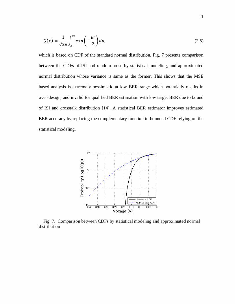
which is based on CDF of the standard normal distribution. Fig. 7 presents comparison
between the CDFs of ISI and random noise by statistical modeling, and approximated
normal distribution whose variance is same as the former. This shows that the MSE
based analysis is extremely pessimistic at low BER range which potentially results in
over-design, and invalid for qualified BER estimation with low target BER due to bound
of ISI and crosstalk distribution [14]. A statistical BER estimator improves estimated
BER accuracy by replacing the complementary function to bounded CDF relying on the
statistical modeling.
Fig. 7. Comparison between CDFs by statistical modeling and approximated normal distribution
12
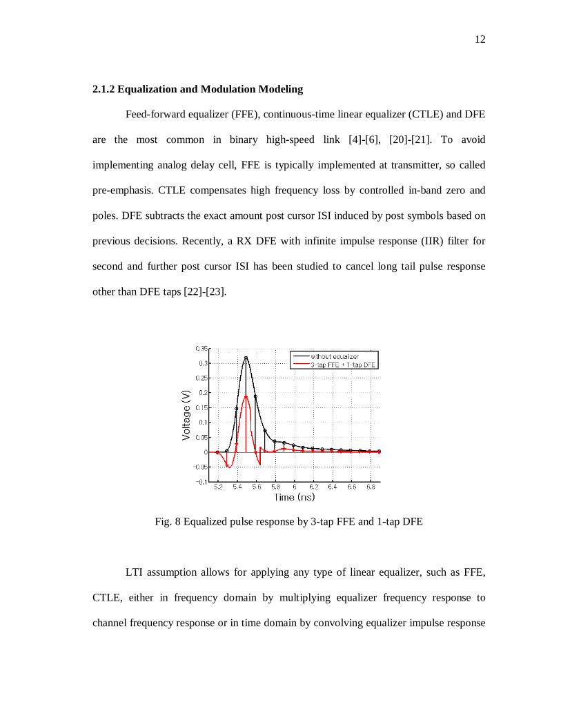
2.1.2 Equalization and Modulation Modeling
Feed-forward equalizer (FFE), continuous-time linear equalizer (CTLE) and DFE
are the most common in binary high-speed link [4]-[6], [20]-[21]. To avoid
implementing analog delay cell, FFE is typically implemented at transmitter, so called
pre-emphasis. CTLE compensates high frequency loss by controlled in-band zero and
poles. DFE subtracts the exact amount post cursor ISI induced by post symbols based on
previous decisions. Recently, a RX DFE with infinite impulse response (IIR) filter for
second and further post cursor ISI has been studied to cancel long tail pulse response
other than DFE taps [22]-[23].
Fig. 8 Equalized pulse response by 3-tap FFE and 1-tap DFE
LTI assumption allows for applying any type of linear equalizer, such as FFE,
CTLE, either in frequency domain by multiplying equalizer frequency response to
channel frequency response or in time domain by convolving equalizer impulse response

13
with channel pulse response. Although DFE is non-linear, ideal functionality without
error propagation due to potential wrong pre-decisions is assumed when achieving low
target BER. Ideal DFE always subtracts the exact amplitude of corresponding post
cursor ISIs for one unit interval (UI) per each DFE tap. Fig. 8 presents the pulse
responses before and after equalization with FFE-DFE. Statistical modeling of residual
ISI after equalization follows the same procedures discussed in previous section with the
equalized pulse response.
Given channel information, FFE coefficients are typically optimized based on
minimum-mean-square-error (MMSE) criteria [19]. Zero forcing FFE has MMSE of ISI
when its coefficients are
𝐶𝑍𝐹−𝐹𝐹𝐸 = (𝐻𝑇𝐻)−1𝐻𝑇𝑌𝑑𝑒𝑠𝑖𝑟𝑒𝑑 , where
𝐻 =
⎣⎢⎢⎢⎡ℎ(0) 0 0 0 0ℎ(1) ℎ(0) 0 0 0⋮ ⋮ ⋮ ⋮ ⋮0 0 0 ℎ(𝑘 − 1) ℎ(𝑘 − 2)0 0 0 0 ℎ(𝑘 − 1)⎦
⎥⎥⎥⎤
, 𝐶𝑍𝐹−𝐹𝐹𝐸 = �
𝑐(0)𝑐(1)⋮
𝑐(𝑙 − 1)
�,
(2.6)
h is k-taps sampled channel pulse response, c is FFE coefficients with l-taps and 𝑌𝑑𝑒𝑠𝑖𝑟𝑒𝑑
is the desired output, such as the vector having 1 for the cursor tap and 0 for all the
others (for PAM modulation). Since FFE scales AWGN either, considerable random
noise should be taken into account. With AWGN, MMSE-FFE coefficients are
optimized when
𝐶𝑀𝑀𝑆𝐸−𝐹𝐹𝐸 = (𝐻𝑇𝐻 + 𝑁)−1𝐻𝑇𝑌𝑑𝑒𝑠𝑖𝑟𝑒𝑑 , (2.7)
14
where N is l by l identical matrix multiplied by variance of independent noise.
Furthermore, with ideal DFE assumption, MMSE-DFE coefficients [24] are optimized
when
𝑊𝑀𝑀𝑆𝐸−𝐷𝐹𝐸 = �𝐻�𝑇𝐻� + 𝑁��−1𝐻�𝑇𝑌𝑑𝑒𝑠𝑖𝑟𝑒𝑑 , where
𝐻� = [𝐻|𝐼𝐷𝐹𝐸], 𝑊𝑀𝑀𝑆𝐸−𝐷𝐹𝐸 =
⎣⎢⎢⎢⎢⎢⎡
𝑐(0)𝑐(1)⋮
𝑐(𝑙 − 1)𝑏(0)⋮
𝑏(𝑚 − 1)⎦⎥⎥⎥⎥⎥⎤
, 𝑁� = �𝑁 00 0�
(2.8)
c and b are l-taps FFE and m-taps DFE coefficients, respectively, and 𝐼𝐷𝐹𝐸 is the matrix
whose components are
𝐼𝐷𝐹𝐸(𝑘, 𝑗) = � 1, if 𝑘 = 𝑘𝑐𝑢𝑟𝑠𝑜𝑟 + 𝑗 0, 𝑜𝑡ℎ𝑒𝑟𝑤𝑖𝑠𝑒.
�
Note that MMSE does not necessarily results in optimal BER when ISI is not controlled
enough, since the ISI PDF differs from a normal distribution PDF as mentioned.
However, it offers useful initial guess for finding optimal equalizer coefficients, and
further optimization can be done by coefficient sweeping in statistical analysis.
Pulse amplitude modulation (PAM) is easily modeled by different transmitting
symbol PDF. For instance, PAM-4 has four symbols, {-1 -1/3 1/3 1} and each ISI tap
has four equiprobable values. Thus, an independent transmitting symbol has four-value
PMF instead of two-value PMF in PAM-2. Equalizer coefficient optimization procedure
is exactly same for any types of PAM. There exist M-1 thresholds for PAM-M and pairs
of thresholds from outer two to inner two excepting zero are symmetric. Ideal thresholds
15
places exactly at the middle of two adjacent constellations, statistical eye opening are the
same for all M-1 thresholds. In practice, thresholds cannot be adapted to non-ideal
sampling point, BER at outer threshold is typically worse than inner one with given
fixed thresholds.
Since duobinary modulator includes a channel [25], MMSE equalizer
coefficients are obtained by simply changing the desired vector to have two cursors
whose values are 0.5 and 0.5 instead of 1 for PAM. Transmitted data is same as PAM-2
but the received signal is
𝑦𝑘 = ℎ0𝐼𝑘 + ℎ1𝐼𝑘+1 + � ℎ𝑛−𝑘𝐼𝑘𝑛≠𝑘,𝑘+1
+ �𝑔𝑚−𝑘𝐼𝑚 + 𝑍𝑘∀𝑚
, (2.9)
where k and k+1 are cursor and the first post cursor, h and g are sampled pulse responses
of through and crosstalk channels, I and 𝐼 are transmitted binary symbols, {1, -1} , and Z
is AWGN. Although duobinary has three possible received symbol, {±(h0 + h1), 0},
mismatch between cursor and the first post cursor separates zero symbol into two and
the distance between constellations is degraded by |h0 − h1|.
2.1.3 Jitter Modeling
While statistical modeling discussed in section 2.1.1-2 is sample-based,
transmitting and sampling timing is not ideal because of jitter at PLL and CDR. Jitter
analysis has been mature with linear modeling of PLL and CDR [14], [26]-[29].
Although phase error of the TX/RX clocks from diverse sources causing jitter in PLL
and CDR is analyzable by jitter transfer function, linearized jitter model often provides

16
too much details with extreme complexity because of various sources of jitter in
clocking circuits that are not necessarily Gaussian distribution [14], and correlation
between TX jitter and RX jitter which is also disturbed by channel ISI, crosstalk and
even DFE subtraction [13]. To simplify statistical analysis, RX jitter is often modeled by
dual-Dirac jitter that approximates jitter distribution as combination of deterministic
jitter (DJ) and random jitter (RJ) [30], and TX jitter is modeled by combination of
periodic and random jitter [14], [31].
(a) (b)
Fig. 9 (a) Thru and crosstalk channel frequency responses [18] and (b) statistical eye
degradation by 2%UI DJ and 2%UIrms RJ of RX jitter
RX jitter distribution in time is transferred to PDF in voltage domain by a family
of PDFs obtained at different sampling timing. Since
𝑃𝑉,𝑇(𝑣, 𝑡) = 𝑃𝑉|𝑇(𝑣|𝑡)𝑃𝑇(𝑡), (2.10)
sum of conditional PDF at the given sampling time multiplied by probability to have that
sampling time is the PDF with RX jitter. Fig. 9(b) presents statistical eye degradation by

17
2%UI of DJ and 2%UI of RJ sigma, which is simulated with the through channel with
two crosstalk channels in Fig. 9(a). The simulation setting are 10Gb/s of data rate, 3-tap
FFE with PAM-2 signaling and 1mVrms random jitter. In Fig. 10, the procedure of
statistical RX jitter modeling and the result is compared to 1k-bit transient simulation
with through channel.
Fig. 10 Procedure of RX jitter modeling and comparison between statistical eye contour referred to 1e-12 of BER and 1k-bit transient simulation eye diagram
TX jitter causes varying TX pulse widths that results in changes of the channel
pulse response. As a result, this does not only affects on RX jitter but also generates
received signal amplitude variation. If TX jitter is totally random and limited to small
variance, random TX jitter is modeled by jitter transfer function from jitter impulse
response. Independent random TX jitter occurs at both of rising and falling edges and
RX signal voltage varies linearly if the TX timing variance is small enough. Thus,
impulse TX timing variance is transferred to jitter sensitivity function (JSF) [14] in
18
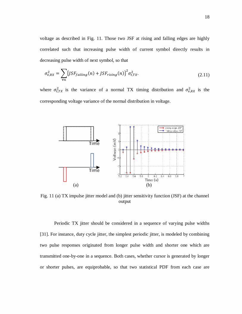
voltage as described in Fig. 11. Those two JSF at rising and falling edges are highly
correlated such that increasing pulse width of current symbol directly results in
decreasing pulse width of next symbol, so that
𝜎𝑣,𝑅𝑋2 = ��𝐽𝑆𝐹𝑓𝑎𝑙𝑙𝑖𝑛𝑔(𝑛) + 𝐽𝑆𝐹𝑟𝑖𝑠𝑖𝑛𝑔(𝑛)�2𝜎𝑡,𝑇𝑋
2
∀𝑛
. (2.11)
where 𝜎𝑡,𝑇𝑋2 is the variance of a normal TX timing distribution and 𝜎𝑣,𝑅𝑋
2 is the
corresponding voltage variance of the normal distribution in voltage.
(a) (b)
Fig. 11 (a) TX impulse jitter model and (b) jitter sensitivity function (JSF) at the channel
output
Periodic TX jitter should be considered in a sequence of varying pulse widths
[31]. For instance, duty cycle jitter, the simplest periodic jitter, is modeled by combining
two pulse responses originated from longer pulse width and shorter one which are
transmitted one-by-one in a sequence. Both cases, whether cursor is generated by longer
or shorter pulses, are equiprobable, so that two statistical PDF from each case are

19
generated and averaged as shown in Fig. 12. This method, however, still requires
demanding tasks as increasing complexity of periodic sequences [13]. Nevertheless,
considering the purpose of statistical analysis, that is providing the qualified guidance
for system-level transceiver design, this modeling is useful by applying proper marginal
conditions with simplified jitter models.
Fig. 12 Procedure for duty cycle TX jitter modeling
2.2 Analog-to-Digital Converter (ADC) Based Link Modeling
Quantization distortion of a uniform ADC is typically modeled as an additive
white uniform distribution whose variance is
𝜎𝑞𝑧2 = 𝐸[(𝑋 − 𝜇)2] = �1𝛥𝑞𝑧
𝑥2𝑑𝑥 =𝛥𝑞𝑧2
12
𝛥𝑞𝑧2
−𝛥𝑞𝑧2
, (2.12)
where ∆𝑞𝑧 is the distance between quantization levels. To simplify analysis, quantization
distortion is often approximated as a normal distribution [9], [10], [12], and BER is
estimated as follows.
𝑆𝑁𝐷𝑅 =𝑃𝑠𝑖𝑔𝑛𝑎𝑙
𝑃𝑛𝑜𝑖𝑠𝑒 + 𝑃𝑑𝑖𝑠𝑡𝑜𝑟𝑡𝑖𝑜𝑛 + 𝑃𝑞𝑢𝑎𝑛𝑡𝑖𝑧𝑎𝑡𝑖𝑜𝑛, and (2.13)

20
𝑃𝑒,𝑃𝐴𝑀2 ≈ 𝑄��𝑑𝑚𝑖𝑛2 /4
𝜎𝑛𝑜𝑖𝑠𝑒2 + 𝜎𝑑𝑖𝑠𝑡𝑜𝑟𝑡𝑖𝑜𝑛2 + 𝜎𝑞𝑢𝑎𝑛𝑡𝑖𝑧𝑎𝑡𝑖𝑜𝑛2 �
= 𝑄 ��ℎ02
∑ ℎ𝑛2𝑛≠0 + ∑ 𝑔𝑚2∀𝑚 + 𝜎𝑍2 + ∆𝑞𝑧2 /12�
= 𝑄�√𝑆𝑁𝐷𝑅 − 1�.
(2.14)
Also, ADC resolution requirements at a given target BER is analyzed relying on the
definition of effective number of bits (ENOB) [16], that is
𝐸𝑁𝑂𝐵 =𝑆𝑁𝐷𝑅 − 1.76
6.02 . (2.15)
Although this is valid when random noise is dominant so that overall noise and
quantization distortion distributes as the closed form of the normal distribution, typical
ADC-based link with limited ADC resolutions to 4-6 bits is not the case.
Previously, in order to improve accuracy for systems with limited quantization
levels, normal and uniform distributions were combined to derive BER for M-PAM with
fading [32]. However, this approach is restricted to analyze the output of the ADC.
When the quantized received signal passes through a following digital FFE, the
quantization error is scaled by FFE coefficients and scaled error distributions at different
sampling times are added up. Since a sum of non-identical uniform distributions has
discontinuous points on its PDF, analytical BER estimation is difficult. This issue is also
discussed in [7], in which it is argued that required noise sigma to achieve BER < 1e-17
is 15~25% of ADC LSB for 3.5bit ADC based on empirical observations, while this is
not a general solution.

21
(a)
(b)
(c)
Fig. 13 (a) Quantization distortion in digital FFE-DFE, (b) proposed statistical modeling for ADC-based receiver with digital FFE-DFE, and (c) comparing statistical modeling
with Gaussian-approximated quantization distortion
In the specific case of digital equalization, digital FFE-DFE (Fig. 13(a)) which is
a common equalizer for low-complexity and power efficient applications, statistical
modeling allows for link performance evaluation without Gaussian approximation. The

22
proposed statistical analysis utilizes the uniformly distributed quantization noise PDFs
scaled by the FFE coefficients for improved BER estimation accuracy with the low ADC
resolutions common in high-speed link systems. A PDF of the sum of the independent
and uniformly distributed random variables is obtained by convolving all the individual
PDFs. This allows for the channel and analog front-end modeling discussed in Section
2.1 to be expanded to the modeling of ADC-based links, as shown in Fig. 13(b). Note
that DFE, which mitigates residual ISI by eliminating corresponding post cursor ISI taps,
does not affect quantization distortion.
The improved BER estimation accuracy by the proposed technique of scaling
quantization error with the FFE coefficients is shown in the bathtub curves at different
ADC resolution settings and FFE tap numbers in Fig. 15-16. For the fair comparison of
the improvement by the proposed method, comparing bathtub curve is generated with
statistical modeling for ISI and Gaussian approximation for quantization distortion (Fig.
13(c)), and digital FFE coefficients are normalized not to scale a normal distribution.
Here, the two quantization distortion modeling techniques of Fig. 13 and also transient
simulation results are compared for a 10Gb/s data rate on two different backplane
channels in Fig. 14. 4/1-tap and 9/1-tap digital FFE/DFEs are used for the channel 1 and
2, respectively. Other simulation settings include the use of PAM-2 signaling, 1mVrms
AWGN, 1Vpp input dynamic range, and 8-bit digital equalizer resolution. To observe the
statistical bound, 1E9 bits are simulated in transient. For this, all three cases are sample-
based simulation, which means the jitter is not considered. However, since jitter in
statistical analysis is applied by combining PDFs built with different transmitting pulse

23
width and sampling time, the verified accuracy in sample-based simulation confirms the
accuracy with jitter. While the interest is the results with 4-6 bits of ADC resolution, 8-
bit ADC is also simulated for sanity check, in which all the three compared cases expect
to be matched.
Fig. 14 Channel frequency responses [18]
As shown in Fig. 15(b)-(d) and Fig. 16(b)-(d), utilizing the proposed quantization
distortion modeling technique allows for improved tracking of transient simulation
results for the typical 4-6 bit ADC resolution settings for high-speed link applications.
Note that when quantization distortion is small, as in Fig. 15(a) and Fig. 16(a) with 8-bit
ADC resolution, both techniques track transient simulation results well. Significance is
Gaussian approximation is often pessimistic and fails to detect large eye opening in Fig.
15(d) that potentially results in over-design. Interestingly, Fig. 16(d) shows possibility of
system fail due to optimistic BER estimation in Gaussian approximation. This is due to

24
the bounded convolution of uniform distributions widening by the absolute sum of the
FFE coefficients, while the variance of the quantization distortion depends on the square
sum of the coefficients. Thus, as the number of FFE taps increases, the magnitude of the
FFE cursor tap increasingly spreads into pre- and post-cursor taps and widens the
quantization distortion bounds.
(a) (b)
(c) (d)
Fig. 15 Bathtub curve comparison at channel 1 in Fig. 14 (a) with 8-bit ADC, (b) 6-bit
ADC, (c) 5-bit ADC, and (d) 4-bit ADC

25
(a) (b)
(c) (d)
Fig. 16 Bathtub curve comparison at channel 2 in Fig. 14 (a) with 8-bit ADC, (b) 6-bit
ADC, (c) 5-bit ADC, and (d) 4-bit ADC

26
CHAPTER III
MODULATION TECHNIQUES AND ANALYSIS
In addition to equalization, modulated signaling allows for controlling ISI over
band-limited channel. Besides, an ADC-based receiver is flexible for different types of
signaling that encourages uses of optimal combinations of equalization and modulation
techniques. Due to limited transceiver complexity by power and area restriction of
compact high-speed I/O applications, a couple of modulation techniques, PAM-4 and
duobinary, have been used in wired communications [25], [29], [33]. In this chapter,
PAM-2, PAM-4 and duobinary are compared by statistical analysis and anticipate the
possible solutions for future ADC-based links.
3.1 Initial Guidance for Modulation Selection
Modulation selection is the critical issue because finding the best performer
among different modulation schemes depends on not only channel loss but also the
distance between signal constellations. While each of PAM-4 and duobinary
performances is compared to PAM-2 in [29], [33], the comparison among three of them
is proposed in [25] with a simple and initial guidance based on effective Nyquist
frequency channel loss. Due to peak power limitation of transmitting signal, maximum
boosting at Nyquist frequency is restricted to 0dB, that is, channel loss at Nyquist
frequency cannot be overcome. Given data rate, PAM-4 has half of symbol rate or half
effective Nyquist frequency compared to PAM-2. Thus, even though ISI is equalized

27
enough for both of cases, PAM-2 suffers from higher channel loss. Controlled ISI by
duobinary provides two third of effective Nyquist frequency reduction.
(a) (b)
Fig. 17 Through and crosstalk channels [18] for (a) case 2 and (b) case 3
However, since PAM-4 and duobinary have four levels and three levels of signal
constellation within given input dynamic, the minimum distances between constellations
are limited by one third and half, respectively. With the assumption of enough
equalization, modulation gain is calculated by subtracting constellation loss from the
gain obtained by relaxed channel loss. For instance, three cases at different channels and
data rates are carefully selected such that each of the cases results in different
modulation selection; case 1 is 10Gb/s at channel in Fig. 9(a); case 2 is 10Gb/s at
channel in Fig. 17(a); case 3 is 8Gb/s at channel in fig. 17(b). Channel losses at effective
Nyquist frequencies and constellation losses are profiled in Table I. Based on the loss
profiles, modulation gain is summarized in Table II. For example, when PAM-4 is used
instead of PAM-2 in case 1, 3.1dB of loss reduction is achieved while the distance
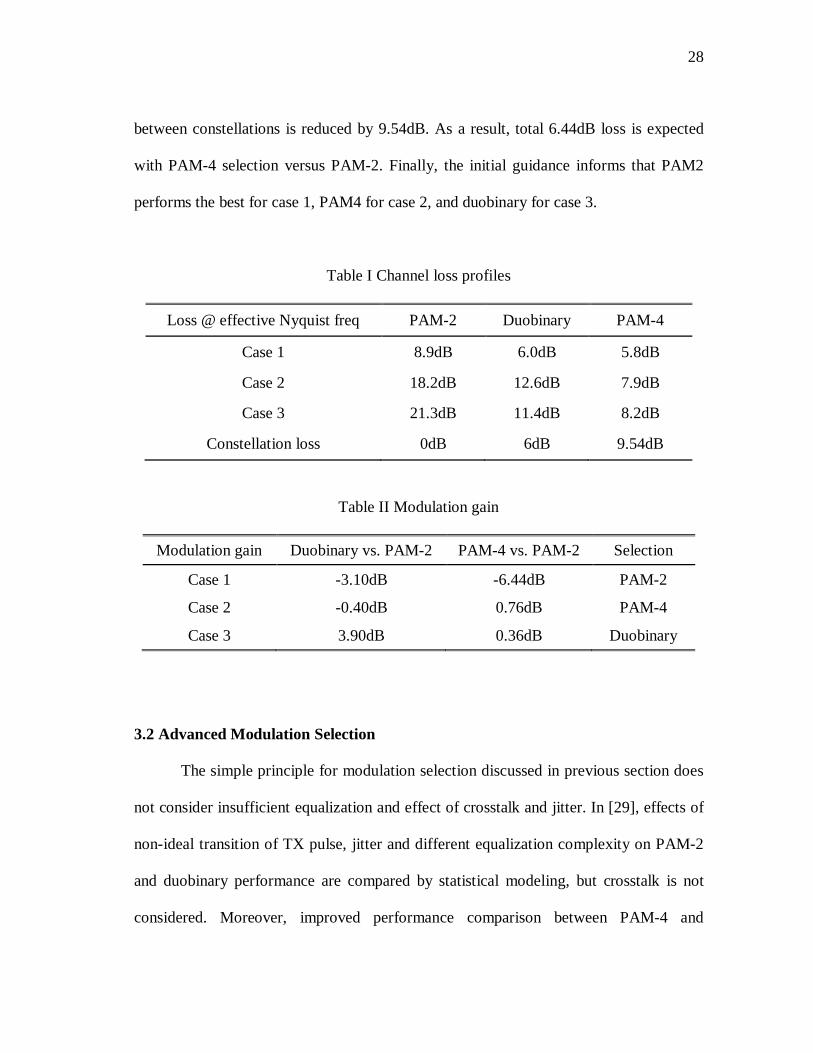
28
between constellations is reduced by 9.54dB. As a result, total 6.44dB loss is expected
with PAM-4 selection versus PAM-2. Finally, the initial guidance informs that PAM2
performs the best for case 1, PAM4 for case 2, and duobinary for case 3.
Table I Channel loss profiles
Loss @ effective Nyquist freq PAM-2 Duobinary PAM-4
Case 1 8.9dB 6.0dB 5.8dB
Case 2 18.2dB 12.6dB 7.9dB
Case 3 21.3dB 11.4dB 8.2dB
Constellation loss 0dB 6dB 9.54dB
Table II Modulation gain
Modulation gain Duobinary vs. PAM-2 PAM-4 vs. PAM-2 Selection
Case 1 -3.10dB -6.44dB PAM-2
Case 2 -0.40dB 0.76dB PAM-4
Case 3 3.90dB 0.36dB Duobinary
3.2 Advanced Modulation Selection
The simple principle for modulation selection discussed in previous section does
not consider insufficient equalization and effect of crosstalk and jitter. In [29], effects of
non-ideal transition of TX pulse, jitter and different equalization complexity on PAM-2
and duobinary performance are compared by statistical modeling, but crosstalk is not
considered. Moreover, improved performance comparison between PAM-4 and

29
duobinary versus PAM-2 is very important to predict future trends in high-speed link
design. From the initial guidance, we know that channel loss range for selecting
duobinary places between those for PAM-2 and PAM-4. In this work, the three
modulation techniques are compared by statistical analysis.
Table III Simulation setting for the three cases in Table I
Input dynamic 1Vppk
Random noise 1mVrms
RX DJ 1%UI
RX RJ 1%UIrms
Target BER 1E-12
Crosstalk FEXT, NEXT
Equalizer 3-tap FFE
Equalizer resolution Ideal
Here, the three cases selected in Table I are reexamined by statistical analysis.
Simulation settings are summarized in Table III and the results are presented in Table
IV-VI, as well as the optimized coefficients of 3-tap FFE by MMSE criteria. Also, from
the statistical eye opening, modulation gain is recalculated and compared in table VII.
As expected, the selected modulation scheme for each case has the largest eye opening.
However, performance differences are not well matched to the estimated modulation
gain by the simple principle presented in Section 3.1. For example, the initial guidance
shows that the expected eye openings for the three modulation schemes in case 3 are

30
similar, but PAM-4 shows remarkable improvement while duobinary has worse
performance than expected. This means, there exists possibility that the selected
modulation scheme is changed by non-ideality of channel and equalizer capability.
Table IV Case 1: FFE coefficients and statistical eye opening
𝑎−1 𝑎0 𝑎1 1e-12 stat.
eye H(mV)
1e-12 stat. eye
W(ps)
PAM2 -0.0492 0.7177 -0.2331 220.4 56 PAM4 -0.0179 0.8824 -0.0997 117.8 80 DUO 0.4951 0.3273 -0.1776 154.7 57
Table V Case 2: FFE coefficients and statistical eye opening
𝑎−1 𝑎0 𝑎1 1e-12 stat.
eye H(mV)
1e-12 stat. eye
W(ps) PAM2 -0.1669 0.5994 -0.2337 14.2 13 PAM4 -0.0470 0.7972 -0.1559 44.4 36 DUO 0.7246 -0.2669 0.0086 8.3 7
Table VI Case 3: FFE coefficients and statistical eye opening
𝑎−1 𝑎0 𝑎1 12-12 stat.
eye H(mV)
1e-12 stat. eye
W(ps)
PAM2 -0.1685 0.5917 -0.2398 54.2 41.25 PAM4 -0.0459 0.7767 -0.1774 58.4 65
DUO 0.7302 -0.2297 -0.0401 62 47.5

31
Table VII Modulation gain by statistical analysis
Modulation gain Duobinary vs. PAM-2 PAM-4 vs. PAM-2 Selection
Case 1 -3.07dB -5.44dB PAM-2
Case 2 -4.66dB 9.90dB PAM-4
Case 3 1.17dB 0.65dB Duobinary
Since equalized frequency response by ideal duobinary has a null at Nyquist
frequency (1/2Tb) as shown in Fig. 18, a band-limited channel is typically included into
the duobinary modulator, which relaxes equalization requirement [25]. Fig. 19 presents
maximum achievable data rate with different complexity of FFE at channel in case 3. As
the number of FFE taps increases, the available data rate also increases in PAM-2 and
PAM-4. However, this trend is not shown in duobinary. Duobinary achieves the highest
data rate with 2-tap FFE due to relaxed equalization requirement, while there is not
notable improvement with increasing FFE taps more than two.
Fig. 18 Pre and post equalized channel frequency responses by 3-tap FFE with PAM-2, PAM-4 and duobinary

32
Fig. 19 Maximum achievable data rate with different number of FFE taps
In addition to limited duobinary transition to the adjacent level, prohibited
patterns in duobinary, {101} and {-10-1}, provide larger voltage margin around ideal
sampling point. However, the duobinary cursor, a combination of two cursors, suffers
from mismatches due to non-ideal sampling timing. Thus, duobinary eye opening is
more quickly degraded than PAM-2 as jitter increases. Clearly, PAM-4 has two times
larger UI than the others, so that it has the best jitter tolerance. Fig. 20 presents the eye
degradation due to increasing random jitter sigma in case 3. As a result, increasing jitter
reduces the duobinary selection range versus PAM-2 and PAM-4.
Finally, crosstalk tolerances in different modulation techniques are analyzed by
statistical modeling. In [33], it is argued that limited transitions to adjacent levels in
duobinary improve immunity to crosstalk and reflection comparing to PAM-2 and PAM-
4. This fact is shown in crosstalk frequency response filtered by FFE in duobinary (Fig.

33
21). However, PAM-4 has diminished average transmitting bit energy by factor of 5/9
since
𝐸𝑏,𝑎𝑣𝑔,𝑃𝐴𝑀4 =14 �
(𝐼)2 + �13 𝐼�
2
+ �−13 𝐼�
2
+ (−𝐼)2� =59𝐸𝑏,𝑎𝑣𝑔,𝑃𝐴𝑀2. (3.1)
Fig. 20 Eye degradation by increasing RX random jitter sigma in case 3
Fig. 21 Crosstalk channel frequency responses filtered by 3-tap FFE in case 3
34
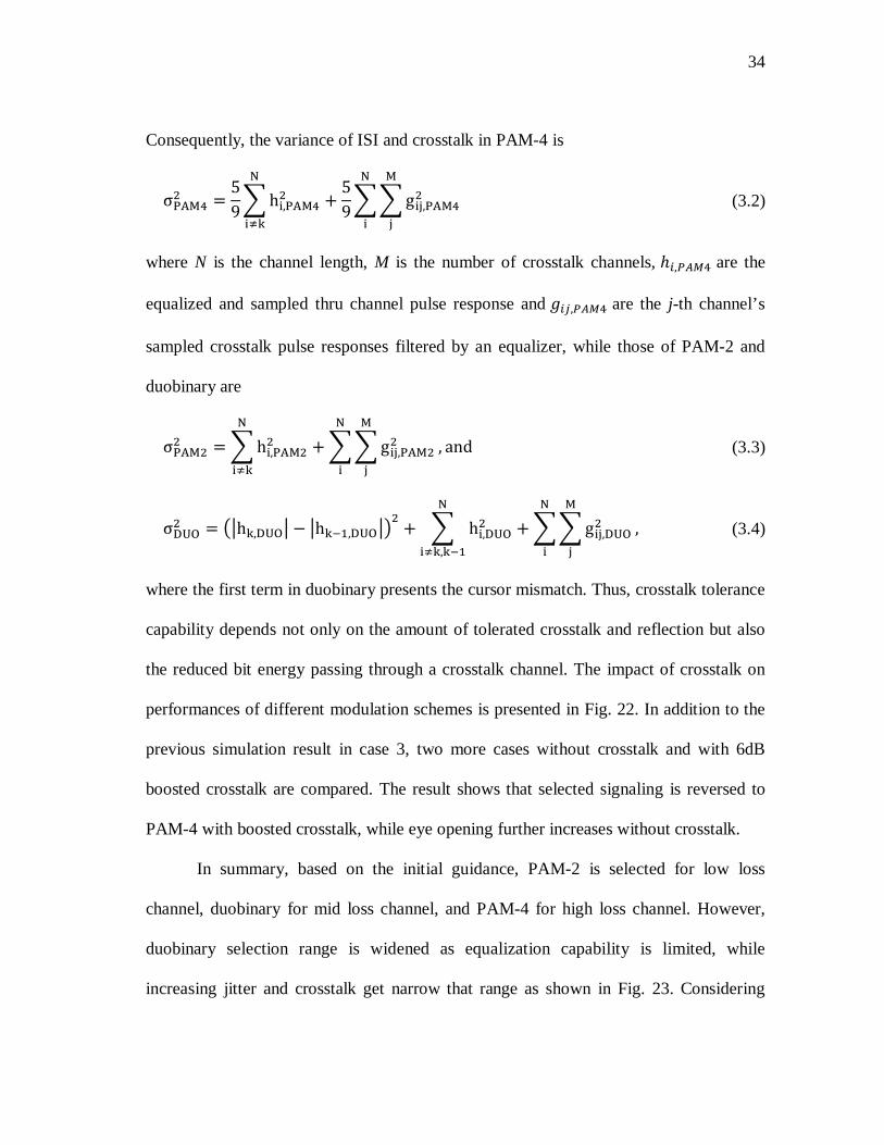
Consequently, the variance of ISI and crosstalk in PAM-4 is
σPAM42 =59� hi,PAM42
N
i≠k
+59�� gij,PAM42
M
j
N
i
(3.2)
where N is the channel length, M is the number of crosstalk channels, ℎ𝑖,𝑃𝐴𝑀4 are the
equalized and sampled thru channel pulse response and 𝑔𝑖𝑗,𝑃𝐴𝑀4 are the j-th channel’s
sampled crosstalk pulse responses filtered by an equalizer, while those of PAM-2 and
duobinary are
σPAM22 = � hi,PAM22N
i≠k
+ �� gij,PAM22M
j
N
i
, and (3.3)
σDUO2 = ��hk,DUO� − �hk−1,DUO��2
+ � hi,DUO2N
i≠k,k−1
+ �� gij,DUO2M
j
N
i
, (3.4)
where the first term in duobinary presents the cursor mismatch. Thus, crosstalk tolerance
capability depends not only on the amount of tolerated crosstalk and reflection but also
the reduced bit energy passing through a crosstalk channel. The impact of crosstalk on
performances of different modulation schemes is presented in Fig. 22. In addition to the
previous simulation result in case 3, two more cases without crosstalk and with 6dB
boosted crosstalk are compared. The result shows that selected signaling is reversed to
PAM-4 with boosted crosstalk, while eye opening further increases without crosstalk.
In summary, based on the initial guidance, PAM-2 is selected for low loss
channel, duobinary for mid loss channel, and PAM-4 for high loss channel. However,
duobinary selection range is widened as equalization capability is limited, while
increasing jitter and crosstalk get narrow that range as shown in Fig. 23. Considering

35
that ADC-based link targets high low channel requiring larger number of FFE to control
significant amount of pre-cursor ISI, jitter and crosstalk become severe as increasing
data rate while enough equalization is applied in DSP. Therefore, PAM-4 is more
promising to use in ADC-based link than duobinary.
Fig. 22 Eye degradation by increasing crosstalk in case 3
Fig. 23 Modulation selection range changes due to limited equalization, jitter and crosstalk

36
CHAPTER IV
EQUALIZATION TECHNIQUES AND ANALYSIS
High-speed ADC power consumption is the most critical bottleneck in ADC-
based receivers to rival binary receivers. ADC resolution requirement as well as its
power dissipation is alleviated either by partially equalizing the signal before
quantization, or by enhancing digital equalizer capability that offers larger margin to
tolerate quantization distortion. This chapter starts with introducing for linear PAE
architectures and evaluating PAE performances on ADC resolution requirement
reduction by statistical analysis. Then, the advanced power efficient ADC-based receiver
architecture is proposed for further saving digital dynamic power consumption. In
addition, a potential use of DFE embedded in ADC as a PAE and its drawbacks are
discussed.
4.1 Linear Partial Analog Equalizer (PAE)
Cascaded analog and digital equalization is initially motivated to use of
additional DFE following analog FFE due to insufficient equalization with limited
analog equalization complexity [34]. As increasing data rate requires more robust
equalization in high-speed wired communications, the idea of partial analog equalizer
(PAE) is extended for general digital equalization, in which main equalization is
performed in digital domain while PAE reduces ADC resolution requirement [12]. Fig.
24 presents signal passed through two cascaded linear equalizers, 2-tap FFE and 6-tap

37
FFE. Although 2-tap FFE is insufficient to have open eye, dynamic range is impressively
limited (Fig. 24(b)) and FSR adjustment allows for relaxing quantization distortion with
reduced ADC input dynamic.
(a) (b) (c)
Fig. 24 1k-bits 10Gb/s PAM-2 eye diagram with (a) channel only, (b) channel + 2-tap FFE, and (c) channel + cascaded 2-tap and 6-tap FFE at a channel with -35.1dB loss
@5GHz
In this work, 3-tap TX FFE (pre-emphasis) [4] and 2-tap sampled-FFE (SFFE)
[35] are considered as linear PAE architectures among different types of existing analog
equalization solutions, considering implementation complexity and power overhead.
Even though continuous-time linear equalizer (CTLE) is also able to serve as a PAE,
CTLE typically has some drawbacks comparing to FFEs. Passive RC CTLE is limited
by impedance discontinuity which potentially causes significant reflection. To relief the
reflection issue, passive LC CTLE is possibly implemented, but inductive network is not
a preferred option for integrated applications [36]. Active CTLE in [20] generates in-
band zero and poles controlled by RC source degeneration for high frequency boosting.
To obtain sufficient Nyquist frequency gain, transconductance and load impedance

38
needs to be increased, while large load impedance significantly limits the bandwidth of
CTLE itself. As a result, active CTLE requires large biasing current or power
consumption. Besides, multiple cascaded stages of CTLE are needed for rapidly
attenuating channel, which also increase further power consumption.
Fig. 25 2-tap TX CML FFE
TX FFE [4] generates controlled transmitting pulses by shared current in multiple
TX drivers. Fig. 25 presents an example of 2-tap TX current-mode logic (CML) FFE.
Since TX signal peak limits maximum total current of drivers, TX FFE coefficients are
normalized by their absolute sum. This means that Nyquist frequency boosting gain to
0dB and corresponding DC loss is unavoidable. Nevertheless, TX drivers sharing total
current do not require additional power consumption and there exists a little power
overhead for latches and coefficient resolution controls. Another important issue is
39
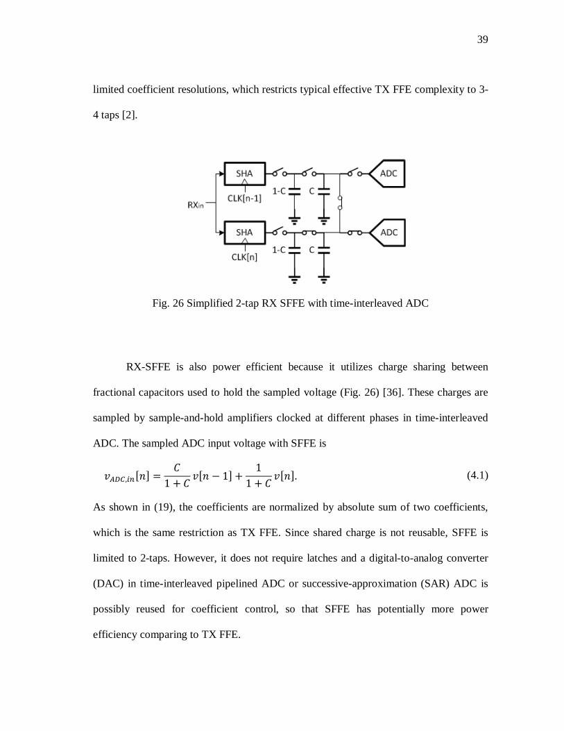
limited coefficient resolutions, which restricts typical effective TX FFE complexity to 3-
4 taps [2].
Fig. 26 Simplified 2-tap RX SFFE with time-interleaved ADC
RX-SFFE is also power efficient because it utilizes charge sharing between
fractional capacitors used to hold the sampled voltage (Fig. 26) [36]. These charges are
sampled by sample-and-hold amplifiers clocked at different phases in time-interleaved
ADC. The sampled ADC input voltage with SFFE is
𝑣𝐴𝐷𝐶,𝑖𝑛[𝑛] =𝐶
1 + 𝐶 𝑣[𝑛 − 1] +
11 + 𝐶 𝑣
[𝑛]. (4.1)
As shown in (19), the coefficients are normalized by absolute sum of two coefficients,
which is the same restriction as TX FFE. Since shared charge is not reusable, SFFE is
limited to 2-taps. However, it does not require latches and a digital-to-analog converter
(DAC) in time-interleaved pipelined ADC or successive-approximation (SAR) ADC is
possibly reused for coefficient control, so that SFFE has potentially more power
efficiency comparing to TX FFE.
40
In previous work [7], ADC resolution requirement reduction with PAE is
analyzed. This previous work compares required ADC resolutions with sampled FFE
and digital DFE to those with digital FFE and digital DFE. However, there is no reason
to limit the use of digital FFE with partial analog FFE. One of the most competitive
advantages of ADC-based receivers is extensibility of equalizer complexity with large
number of FFE taps, which allows for effectively canceling both of pre and post cursor
ISI over high channel attenuation. Moreover, the simulated channel losses range from
15.2dB to 34.5dB at 5GHz of Nyquist frequency. Although these results provides a
guidance how ADC-based receivers rival to binary receivers in terms of power and area
complexity, more interest is higher data rate and channel attenuation, in which ISI
control by analog FFE and multi-tap DFE is extremely challenging. This motivates our
work to explore PAE performance at 12.5Gb/s data communications over higher loss
channels up to 46.4 dB at Nyquist frequency.
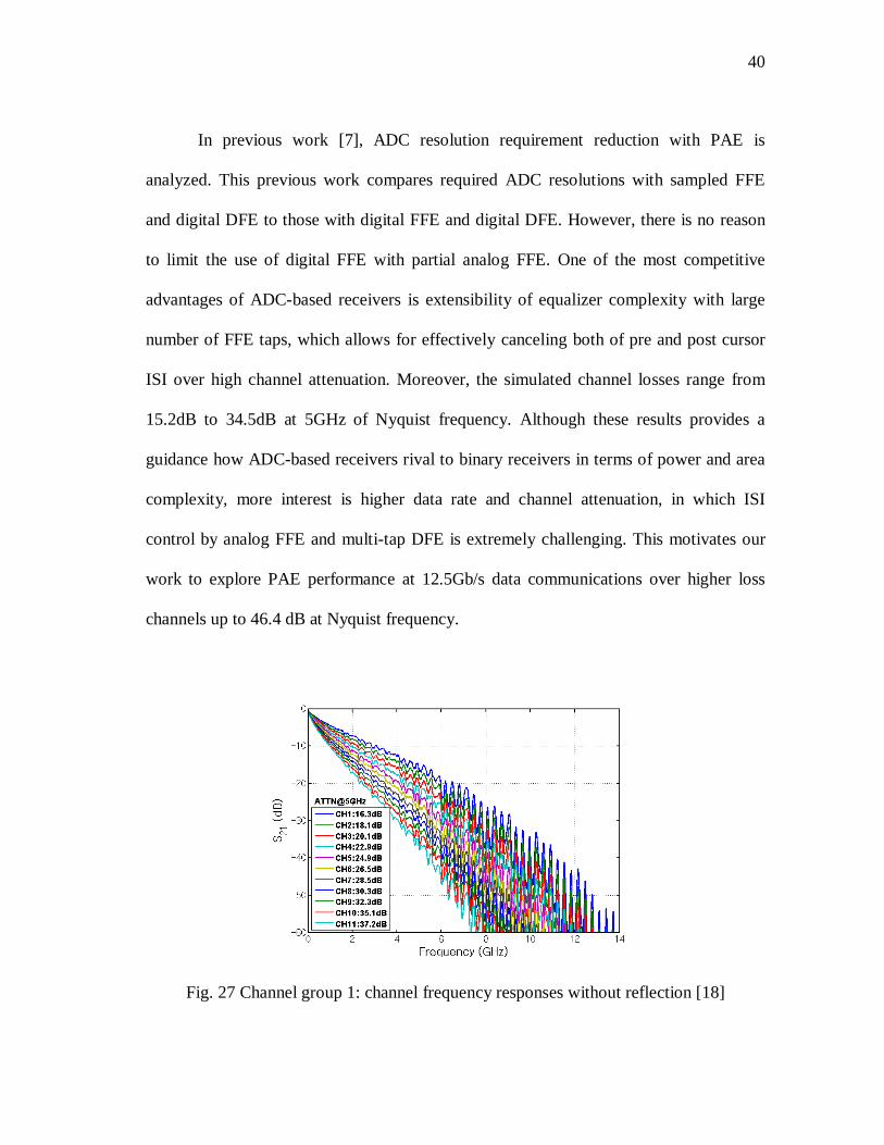
Fig. 27 Channel group 1: channel frequency responses without reflection [18]
41
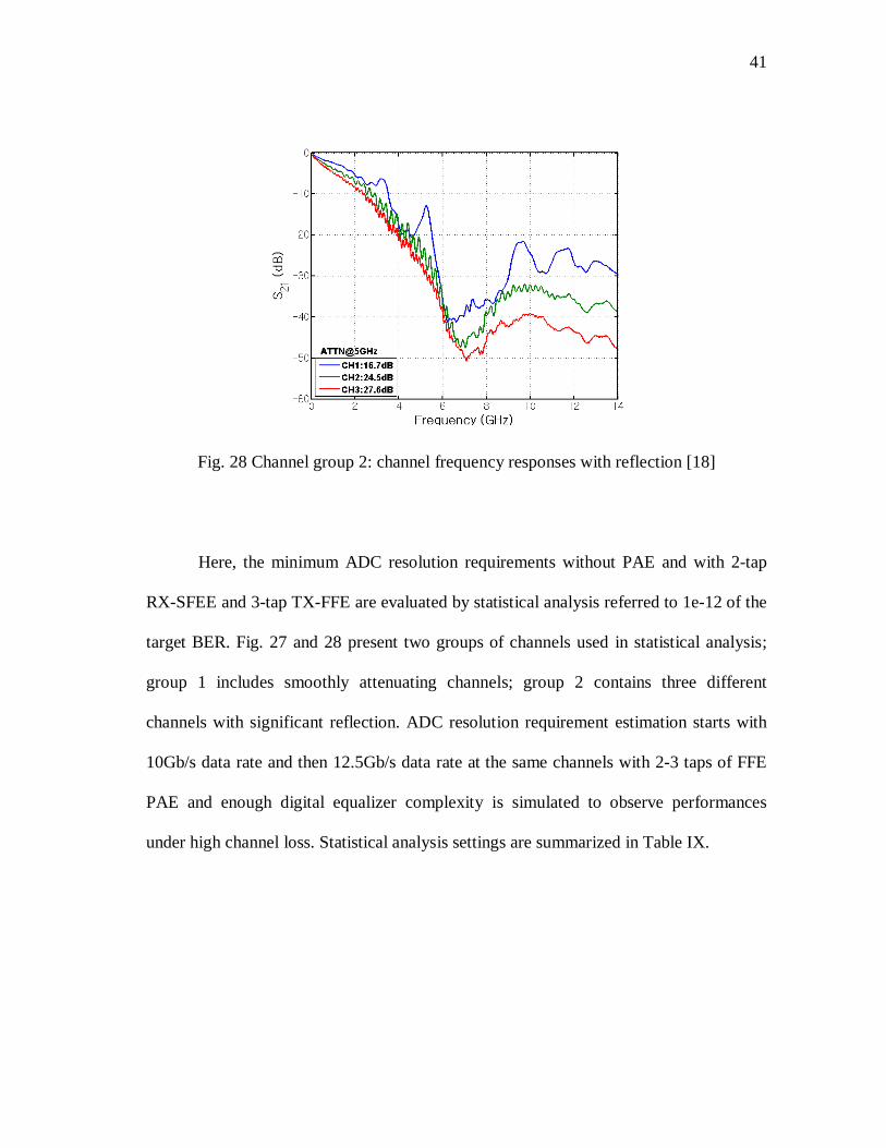
Fig. 28 Channel group 2: channel frequency responses with reflection [18]
Here, the minimum ADC resolution requirements without PAE and with 2-tap
RX-SFEE and 3-tap TX-FFE are evaluated by statistical analysis referred to 1e-12 of the
target BER. Fig. 27 and 28 present two groups of channels used in statistical analysis;
group 1 includes smoothly attenuating channels; group 2 contains three different
channels with significant reflection. ADC resolution requirement estimation starts with
10Gb/s data rate and then 12.5Gb/s data rate at the same channels with 2-3 taps of FFE
PAE and enough digital equalizer complexity is simulated to observe performances
under high channel loss. Statistical analysis settings are summarized in Table IX.
42
Table IX Simulation settings for ADC resolution requirement
Signaling PAM-2
Data rate 10Gb/s and 12.5Gb/s
Input dynamic 1Vppk
Random noise 1mVrms
RX DJ 2%UI
RX RJ 2%UIrms
Target BER 1E-12
ADC res. 3-8 bits
PAE No / 2-tap FFE / 3-tap FFE
PAE res. 5 bits
Digital equalizer 4/1-tap FFE/DFE 6/1-tap FFE/DFE
12/2-tap FFE/DFE (reflective channels)
Digital equalizer res. 1 bit greater than ADC res.
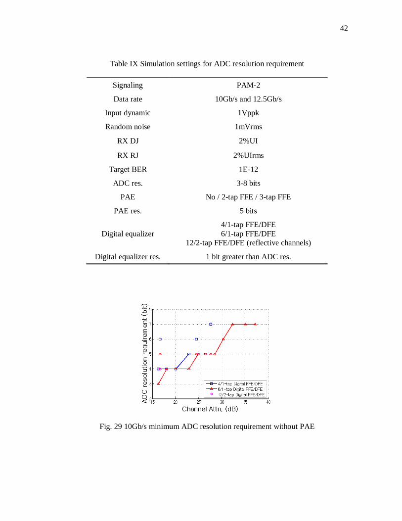
Fig. 29 10Gb/s minimum ADC resolution requirement without PAE

43
Fig. 30 10Gb/s minimum ADC resolution requirement with 2-tap FFE PAE
Fig. 31 10Gb/s minimum ADC resolution requirement with 3-tap PAE
Fig. 29 to 31 shows the results of required ADC resolution reduction by PAE at
10Gb/s. Connected data points are from the smoothly attenuating channel group 1 in Fig.
27 and separated points are from reflective channel group 2 in Fig. 28. ADC-based
receivers without PAE require high ADC resolutions as shown in Fig. 29, which
44
discourages to choose ADC-based receivers against binary receivers. Although all the
simulated channels can be equalized enough by 3-tap analog FFE and 3-tap DFE, an
ADC based receiver with 4-tap digital FFE and 1-tap DFE limitedly tolerates up to
28.5dB of channel loss within 8-bit ADC resolution. To overcome 37.2dB of channel
loss, 7-bit ADC and 6/1-tap digital FFE/DFE is required. Besides, channel reflection
requires further increasing equalization complexity. 4/1 tap and 6/1 tap digital FFE/DFE
are not sufficient for equalizing the three reflection channels and need 1-2 bits more of
ADC resolution comparing to gently attenuating channels having similar channel loss.
With PAE, however, ADC resolution requirements are impressively mitigated at
smoothly attenuating channels. Without reflection, up to 4 bits of resolution requirement
reduction is achieved by 2-tap RX SFFE (Fig. 30) and 3-tap TX FFE accomplishes
maximum 5 bits of ADC resolutions saving at over 35dB of channel loss (Fig. 31). An
importance observation is that significant reflection causing resonant null at lower
frequency than Nyquist frequency (channel 1 in group 2) deadly degrades PAE
performance. In this case, increasing digital equalizer complexity improve ADC
resolution requirement more efficiently than PAE. Overall, with maximum complexity
for both digital equalizer and PAE, only 4-bit ADC resolution is needed for all the
channels.

45
Fig. 32 12.5Gb/s minimum ADC resolution requirement with 6/1-tap digital FFE/DFE and No/2/3-tap PAE at channel 6-11 in group 1
Fig. 33 12.5Gb/s minimum ADC resolution requirement with 12/2-tap digital FFE/DFE
and No/2/3-tap PAE at channel 1-3 in group 2
Simulation results with 12.5Gb/s data rate at channel 6-11 in channel group 1 and
at channel 1-3 in channel group 2 are presented in Fig. 32 and Fig. 33. In these cases,
channel attenuations range from 34.4dB to 46.4dB. Digital equalizer complexities are
selected to 6/1-tap FFE/DFE for channel group 1 and 12/2-tap FFE/DFE for channel
46
group 2 for enough digital equalization to achieve optimal ADC resolution reduction by
PAE. The other simulation settings are the same as the previous 10Gb/s cases in Table
IX. Note that as channel loss exceeds over 40dB, 12.5Gb/s data suffers from extreme
pre-cursor ISI which is uncontrollable by only 3-tap analog FFE. If limited-tap FFE
aggressively forces to cancel the pre-cursor ISI, cursor amplitude is significantly reduced
and post-cursor ISI gets even worse. ADC-based receiver with 3-tap FFE PAE,
meanwhile, requires only 5-bit ADC resolution over all the channels. Considering
growing requirement for large number of FFE taps for pre-cursor ISI and reasonable
ADC complexity with PAE, it is expected that ADC-based high-speed link will become
the main stream in future wired communication with continuously increasing data rate as
long as electrical channel is used.
4.2 Hybrid Architecture
Although PAE improves ADC power consumption by alleviate resolution
requirement, it also limits SNDR due to attenuated cursor amplitude in addition to
channel loss and quantization distortion. This leads potential increasing digital equalizer
complexity to overcome degraded SNDR. Consequently, power consumption of heavy
digital equalizer is going to become as considerable as high-speed ADC power
dissipation. Meanwhile at the input of the ADC, a signal does not include quantization
distortion even though it is not sufficiently equalized by PAE. This means that signal
integrity with PAE at the input of the ADC may not excessively differ from that after
fully equalized by digital equalizer.

47
(a) (b)
Fig. 34 Statistical bathtub curves (a) with open-eye and (b) with closed-eye
The proposed hybrid architecture is motivated to make the utmost use of the
information from the ADC output signal. Fig. 34 presents two statistical bathtub curves
with PAM-2 signaling, one has an open eye (Fig. 34(a)) and the other has a closed eye
(Fig. 34(b)) referring 1E-12 of the target BER. The later may fail to achieve the target
BER if decisions are made relying on the zero-threshold; however, there still exists
reliable region. For instance, if a received signal is low enough than a certain negative
threshold, the probability that is originated from ‘1’ transmitting symbol is lower than
the target BER. Likewise, high enough signal most probably comes from ‘1’ symbol
without any additional equalization. Therefore, the proposed hybrid receiver defines the
region between certain threshold voltages as the unreliable region and selectively
equalizes only unreliable signals in digital in order to save dynamic digital power
consumption.
48
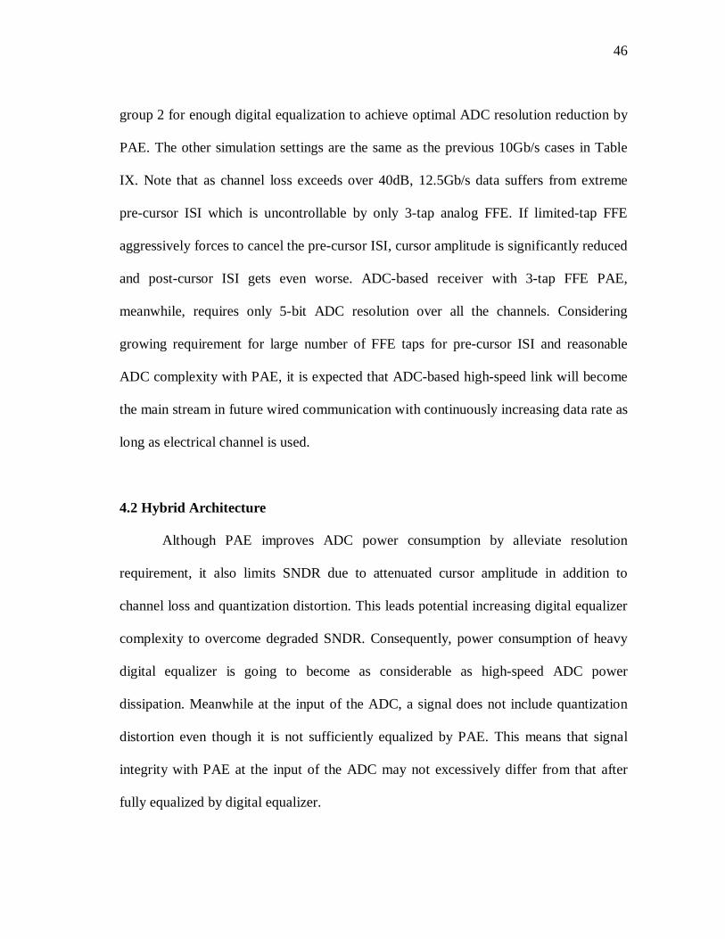
There are two possible types of selective equalization, channel-by-channel
selection and symbol-by-symbol selection. The former is the case having open eye with
PAE in some channels when a transceiver communicates through multiple channels. In
this case, a majority of ADC power is saved by limiting ADC to generate only MSB.
Although this provides better programmability for multi-channel communications,
channel properties are typically known and fixed in wired communications. This more
motivates symbol-by-symbol selection.
Fig. 35 Proposed hybrid architecture
The proposed hybrid architecture targets high attenuation channels in which PAE
does not sufficiently equalizes ISI but enhances ADC resolution requirement. Fig. 35
describes the hybrid receiver. Threshold detector takes the output of ADC and outputs
‘high’ if the received signal is between thresholds. Then, latches passes received signal
in pipelined registers through a digital equalizer and select multiplexer to take the
decision from the digital equalizer. Otherwise, digital equalizer input is fixed, so that
49
there is no dynamic power consumption in digital equalizer. In this case, decision is
made by MSB of the ADC outputs in memory. Power overheads are from threshold
detector, multiplexer and latches and delay cells to synchronize threshold detector with
digital equalizer.
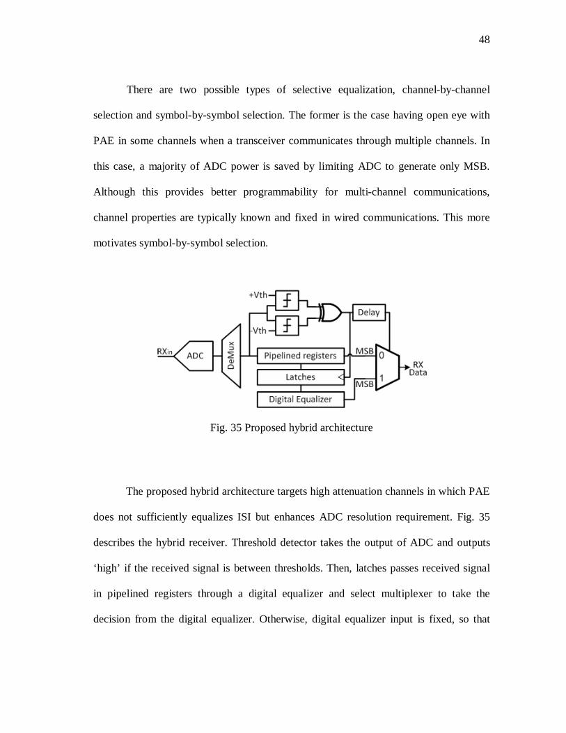
Fig. 36 presents hybrid receiver power efficiency at 10Gb/s with channels in Fig.
27 and 28, in terms of the ratio of disabled digital equalizer versus enabled. Thresholds
are obtained by statistical analysis with the same simulation settings in Table IX. Power
efficiency is estimated by 1M bits of transient simulation because statistical analysis is
not accurate for highly probable events due to correlations between unequalized symbols.
Without PAE, power efficiency is rapidly degraded as channel loss increases because of
large variance of ISI but PAE dramatically improves power efficiency of hybrid
architecture.
Fig. 36 10Gb/s digital equalization power saving efficiency with No/2/3-tap FFE PAE

50
Fig. 37 12.5Gb/s digital equalization power saving efficiency with 2/3-tap FFE PAE
Despite impressive achievement in digital equalization power saving, ADC is
always working so that overall power consumption may be much larger than a simple
binary receiver with a few taps of additional DFE in 10Gb/s cases. More interestingly,
power efficiency in Fig. 37 obtained with 12.5Gb/s data rate still shows impressive
power efficiency, even with considerable complexity of required digital equalizer
complexity. As mentioned in previous section, in these channels requires 6/1-tap digital
FFE/DFE for smoothly attenuating channel and 12/2-tap digital FFE/DFE for channels
with significant reflection. In all the ranges up to 46.4dB of channel loss, at least 64% of
power efficiency is achieved. Another important finding is that the simulation result at
reflective channel 1 implies MMSE does not necessarily results in optimal power saving.
It is because PAE FFE coefficients are simply optimized by MMSE algorithm, and
insufficient equalization by PAE causes significant residual ISI whose PDF does not

51
fallow a normal distribution. This requires custom optimization to achieve optimal
power efficiency, such as parametric sweep by statistical analysis.
4.3 Decision Feedback Equalizer (DFE) for Partial Equalization
A couple of previous works propose embedded DFE into pipelined ADC [37],
and SAR ADC [35]. These applications are time-interleaved ADC and utilize MSB of
the previously sampled symbol at neighbor time-interleaved ADC as the reference for
DFE subtraction. While the embedded-DFE approaches allow DFE to be efficiently
implemented with a little power overhead, the use of those ADC output has to be
carefully considered. Although the full resolution ADC outputs can potentially be used
for FSR or digital CDR, the interest in this work is their possibility to serve as PAE.
Simple calculation of error probability with embedded-DFE and following digital
equalizer predicts that these architectures are not efficient for PAE, because DFE
subtraction relies on pre-decision at the output of ADC, not the final decision after
digital equalization. Assuming that p is the probability of previous wrong decision at
embedded-DFE, q is final error probability after digital equalization with previous
correct decision, and r is that with previous wrong decision, then the total error
probability is,
𝑃𝑒 = (1− 𝑝)𝑞 + 𝑝𝑟. (4.2)
Here exists contradiction. Since a wrong decision doubles corresponding post-cursor ISI,
both of q and r cannot be reduced by fixed digital equalization. Also, p less than the
52
target BER means no need of additional equalization. Thus, the overall error probability
is significantly limited.
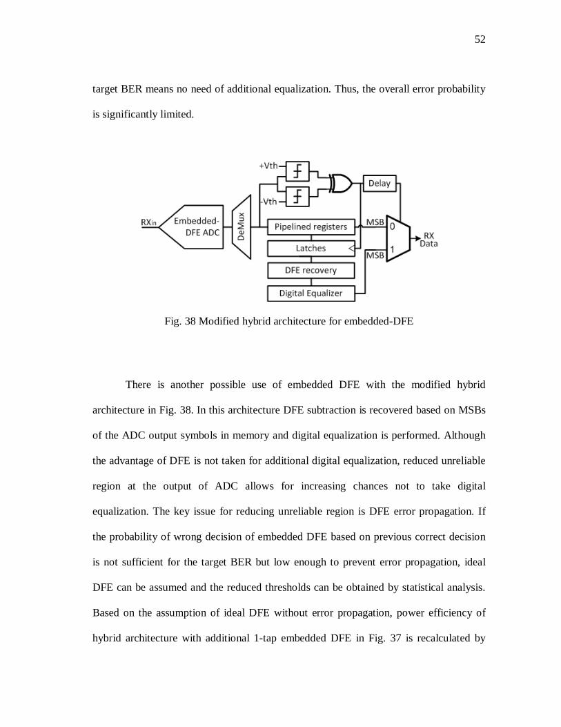
Fig. 38 Modified hybrid architecture for embedded-DFE
There is another possible use of embedded DFE with the modified hybrid
architecture in Fig. 38. In this architecture DFE subtraction is recovered based on MSBs
of the ADC output symbols in memory and digital equalization is performed. Although
the advantage of DFE is not taken for additional digital equalization, reduced unreliable
region at the output of ADC allows for increasing chances not to take digital
equalization. The key issue for reducing unreliable region is DFE error propagation. If
the probability of wrong decision of embedded DFE based on previous correct decision
is not sufficient for the target BER but low enough to prevent error propagation, ideal
DFE can be assumed and the reduced thresholds can be obtained by statistical analysis.
Based on the assumption of ideal DFE without error propagation, power efficiency of
hybrid architecture with additional 1-tap embedded DFE in Fig. 37 is recalculated by

53
statistical analysis. Fig. 39 shows that additional 1-tap DFE achieves maximum 27% of
power efficiency improvement comparing to the case without DFE.
Fig. 39 12.5Gb/s digital equalization power saving efficiency with 2/3-tap FFE and 1-tap ideal DFE PAE
Now, the important two issues are how much pre-decision quality is required for
assumption of ideal DFE without error propagation and how the threshold voltage
changes if error propagation is not negligible. The most common approach for
evaluating error propagation is Markov chain analysis [38]. However, it is not applicable
for this case because of exponentially increasing computational complexity with
significant amount of residual ISI after PAE. In this work, symbol-based transient
simulation with 1Gbits of data is performed and compared to the statistical analysis with
ideal DFE assumption to determine minimum requirement of the pre-decision BER at
54
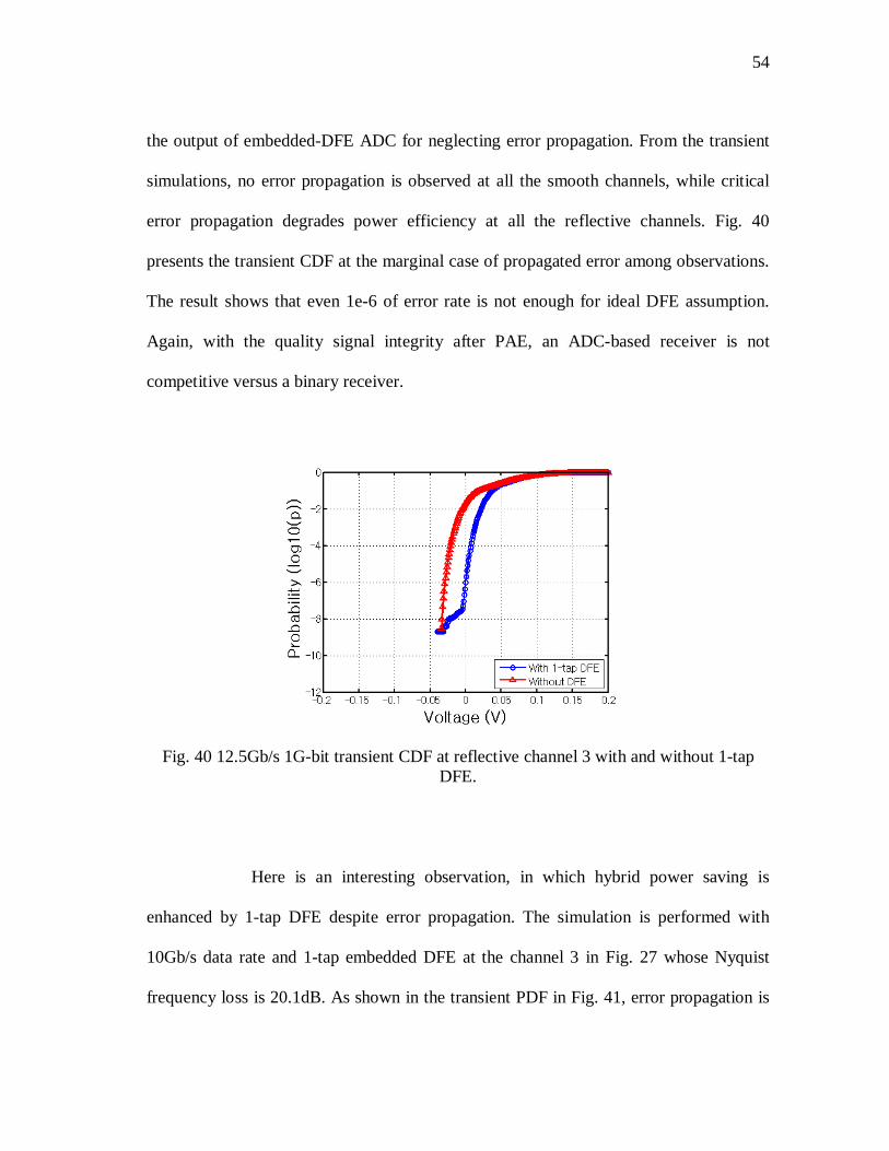
the output of embedded-DFE ADC for neglecting error propagation. From the transient
simulations, no error propagation is observed at all the smooth channels, while critical
error propagation degrades power efficiency at all the reflective channels. Fig. 40
presents the transient CDF at the marginal case of propagated error among observations.
The result shows that even 1e-6 of error rate is not enough for ideal DFE assumption.
Again, with the quality signal integrity after PAE, an ADC-based receiver is not
competitive versus a binary receiver.
Fig. 40 12.5Gb/s 1G-bit transient CDF at reflective channel 3 with and without 1-tap DFE.
Here is an interesting observation, in which hybrid power saving is
enhanced by 1-tap DFE despite error propagation. The simulation is performed with
10Gb/s data rate and 1-tap embedded DFE at the channel 3 in Fig. 27 whose Nyquist
frequency loss is 20.1dB. As shown in the transient PDF in Fig. 41, error propagation is

55
observed and tail probability is extrapolated by polynomial curve fitting to estimate
modified threshold with error propagation. Extended tail provides a new threshold to
define unreliable region referred to 1e-12 of probability. Based on the new threshold
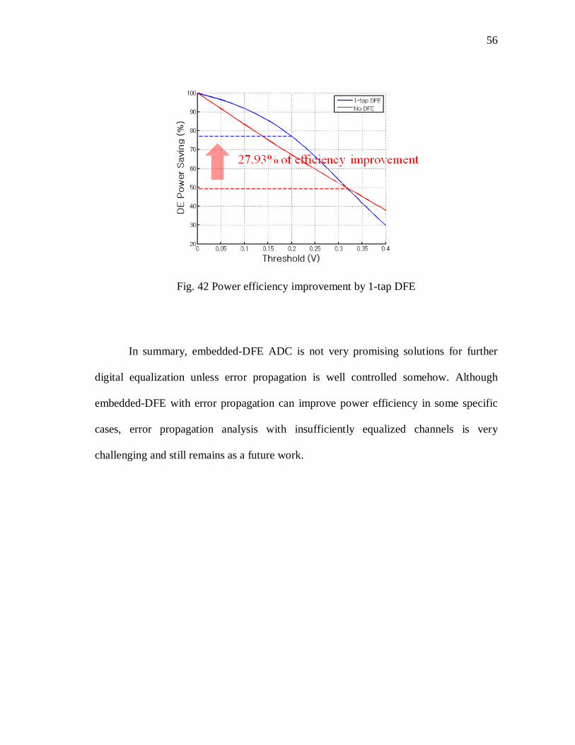
with 1-tap DFE, Fig. 41 shows the power efficiency improvement comparing to the case
without DFE in Fig. 36. Interestingly, 1-tap DFE reduces the threshold from 0.32V to
0.02V and 27.93% of efficiency improvement is achieved even though error propagation
happens. Note that this improvement only shows that the percentage of dynamic power
saving by fixing digital equalizer input. Due to additional power overhead for DFE
subtraction recovery, the actual power saving will be degraded. The observed power
efficiency improvement is because error propagation limits some worst case data
patterns for residual ISI. Since a propagated error from the same polarity of previous
symbol rather helps the current decision, errors propagate only with limited data
sequences.
(a) (b)
Fig. 41 (a) Transient simulation PDF and (b) its CDF and tail extrapolation with 10Gb/s
data rate and 1-tap DFE at channel 3 in Fig. 27.
56
Fig. 42 Power efficiency improvement by 1-tap DFE
In summary, embedded-DFE ADC is not very promising solutions for further
digital equalization unless error propagation is well controlled somehow. Although
embedded-DFE with error propagation can improve power efficiency in some specific
cases, error propagation analysis with insufficiently equalized channels is very
challenging and still remains as a future work.
57
CHAPTER V
CONCLUSION AND FUTURE WORK
In conclusion, this work presents a statistical modeling for ADC-based links with
digital FFE-DFE equalizers. Three cases of digital equalization with 4-6 bit ADC are
simulated and compared with Gaussian approximation based analysis and transient
simulation results. The results show that Gaussian approximation is often pessimistic
due to unbounded tail probability, but it is also possibly optimistic with large variance of
quantization distortion and large number of FFE taps. Proposed modeling better tracks
the actual observations in transient simulation and helps avoid potential over-design or
system fail to satisfy the low target BER.
ISI control and mitigation can be achieved either by using advanced signaling or
by equalization. Since PAM-4 and duobinary worsen eye opening for low-loss channels,
modulation scheme should be carefully selected. From the simple profiling of channel
attenuation profiling, the best performing signaling can be selected. However,
insufficient equalization complexity, jitter and crosstalk possibly change the initial
modulation selection. Specifically, limited equalization encourages duobinary selection,
while jitter and crosstalk increases the chance to select PAM-4.
Power and area consumption of high-speed ADC is the most critical bottle neck
for ADC-based links. However, in future high-speed link with further increasing data
rate, extremely increasing demands for equalization more motivates to take the
advantages of DSP. PAE is a very promising solution to alleviate ADC resolution
58
requirement so as to reduce high-speed ADC power and area consumption. This work
presents that 12.5Gb/s data communication in channels having up to 46dB of loss
requires only 5-bit ADC with 3-tap FFE PAE and 6/1-tap digital FFE/DFE. Even with
significant channel reflection, 5-bit ADC with 3-tap FFE PAE and 12/2-tap digital
FFE/DFE can endure up to 43dB of channel loss at 12.5Gb/s data rate. Moreover, PAE
also improves additional power digital saving with hybrid architecture. With 3-tap PAE,
at least 64% of dynamic power saving is achievable in all the cases simulated in this
work. Meanwhile, DFE cannot serve as a PAE, but can be used in hybrid architecture
with DFE recovery. However, the power saving performance with DFE is significantly
limited by error propagation.
Overall, ADC-based link will become a main stream of high-speed transceiver in
future wired communication as long as electrical channel is used. Considering ADC-
based receivers target high attenuating channel with large data rate and provide robust
equalization capability, a combination of PAM-4 and ADC-based receiver is the most
promising solution for future high-speed I/O links. In addition, enhanced power
efficiency by PAE and hybrid architecture will make this change earlier.
5.1 Future Work
This work could be extended to diverse advanced researches. In this section,
some of possible extensions of research are presented. First of all, ADC-based link with
PAM-4 suffers from additional SNDR degradation due to constellation loss. This may
motivate advanced digital equalizer beyond FFE-DFE, such as maximum-likelihood
59
sequence estimator (MLSE) [19]. However, MLSE is non-linear equalizer so that
statistical analysis is challenging with MLSE. Although one possible analysis approach
is Markov chain modeling, this typically becomes extremely complicated with large taps
of channel modeling with uncontrolled ISI.
Secondly, actual power modeling is not included in this work. It is clear that
ADC-based link performs better with high channel attenuation while binary receiver
may be preferred for low loss channels. Thus, power break-even point between them in
terms of channel loss and data rate needs to be analyzed. Actual power saving from
hybrid architecture is still not clear because digital equalizer power itself may not be
significant comparing to ADC power, and dynamic power consumption for enabling and
disabling digital circuits in hybrid architecture is often critical.
Thirdly, the hybrid architecture with embedded-DFE and error propagation
mitigation techniques could be further researched as well as its statistical modeling. Here
are examples of previously proposed approaches to relax error propagation. In [39],
erasure-DFE is proposed, which is similar idea to hybrid receiver but DFE subtraction is
selectively taken based on a certain thresholds. Also, pre-coded data can help to alleviate
error propagation [40]. The advantage of coding method is that this does not increase
structural complexity of transceivers.
Finally, due to significant channel loss and additional constellation loss with
PAM-4, actual implementation of ADC having tiny LSB for optimal FSR could be
challenging. Generally, small LSB of ADC is not favorable because of many design
issues such as current injection from non-ideal CMOS switch, limited input sensitivity of

60
clocked comparator and inductive kickback to sampled ADC input. Variable gain
amplifiers (VGAs) can help this issue, but limited high frequency gain and bandwidth
makes implementation difficult as well as generated noise by VGAs. Thus, resolution
requirement reduction is potentially limited by non-ideal FSR adjustment and achievable
enhancement in reality could be explored.

61
REFERENCES
[1] W. J. Dally and J. W. Poulton, Digital Systems Engineering, Cambridge, UK,
Cambridge Univ. Press, 1998.
[2] B. Casper, J. Jaussi, F. O’Mahony, M. Mansuri, K. Canagasaby, et al., ‘A 20Gb/s
forwarded clock transceiver in 90nm CMOS,’ IEEE ISSCC, Feb., 2006, pp. 263-
272.
[3] D. Hernandez-Garduno and J. Silva-Martinez, “A CMOS 1Gb/s 5-tap transversal
equalizer based on inductorless 3rd-order delay cells,” IEEE ISSCC, Feb., 2007, pp.
232-599.
[4] R. Payne, P. Landman, B. Bhakta, S. Ramaswamy, S. Wu, et al, “A 6.25Gb/s
binary transceiver in 0.13-um CMOS for serial data transmission across high loss
legacy backplane channels,” IEEE JSSC, vol. 40, no. 12, Dec., 2005, pp. 2646-
2657.
[5] M. Park, J. Bulzacchelli, M. Beakes and D. Friedman, “A 7Gb/s 9.3mW 2-tap
current-integrating DFE receiver,” IEEE ISSCC, Feb., 2007, pp. 230-599.
[6] T. Toifl, C. Menolfi, M. Ruegg, R. Reutemann, A. Prati, et al, “A 2.6mW/Gbps
12.5Gbps RX with 8-tap switched-cap DFE in 32nm CMOS,” IEEE VLSIC, June,
2011, pp. 210-211.
[7] E. Chen and C. K. Yang, “ADC-based serial I/O receivers,” IEEE TCAS-I, vol. 57,
no. 9, Sept. 2010, pp. 2248-2258.
62
[8] M. Harwood, N. Warke, R. Simpson, T. Leslie, A. Amerasekera, et al, “A
12.5Gb/s SerDes in 65nm CMOS using a baud-rate ADC with digital receiver
equalization and clock recovery,” IEEE ISSCC, Feb., 2007, pp. 436-591.
[9] H. Chung and G. Wei, “Design-space exploration of backplane receivers with
high-speed ADCs and digital equalization,” IEEE CICC, Sep., 2009, pp. 555-558.
[10] J. Kim, J. Ren, B. S. Leibowitz, P. Satarzadeh, A. Abbasfar, et al, “Equalizer
design and performance trade-offs in ADC-based serial links,” IEEE TCAS-I, vol.
58, no. 9, Sep., 2011, pp. 2096-2107.
[11] O. Tyshchenko, A. Sheikholeslami, H. Tamura, Y. Tomita, H. Yamaguchi, et al,
“A fractional-sampling-rate ADC-based CDR with feedforward architecture in
65nm CMOS,” IEEE ISSCC, Feb., 2010, pp. 166-167.
[12] A. Hadji-Abdolhamid, “Partial analog equalization and ADC requirements in
wired communications,” Ph. D. Thesis, Univ. of Toronto, 2004.
[13] G. Balamurugan, B. Casper, J. E. Jaussi, M. Mansuri, F. O’Mahony, et al,
“Modeling and analysis of high-speed I/O links,” IEEE Trans. On Adv. Pack., vol.
32, no. 2, May 2009, pp 237-247.
[14] Vladimir Stojanovic, “Channel-limited high-speed links: modeling, analysis and
design,” Ph. D. Thesis, Stanford Univ., 2004.
[15] A. Sanders, M. Resso and J. D’Ambrosia, ‘Channel compliance testing utilizing
novel statistical eye methodology,’ DesignCon, 2004. [Online]. Available:
http://www.stateye.org, Accessed: Mar., 2011.
63
[16] Y. Geerts, Design of multi-bit delta-sigma A/D converters, Boston, MA, Kluwer
Academic Publishers, 2002.
[17] Agilent Tech, “Agilent AN 154 s-parameter design,” Application Note, May, 2005.
[Online]. Available:http://www.cp.literature.agilent.com/litweb/pdf/5952-1087.pdf,
Accessed: Mar., 2011.
[18] IEEE P802.3ap Task Force, Channel Model Material. [Online]. Available:
http://www.ieee802.org, Accessed: Mar., 2011.
[19] J. G. Proakis, Digital Communications, Boston, MA, McGraw-Hill, 2008.
[20] S. Gondi and B. Razavi, “Equalization and clock and data recovery techniques for
10-Gb/s CMOS serial-link receivers,” IEEE JSSC, vol. 42, no. 9, Sep., 2007, pp.
1999-2011.
[21] A. Rylyakov and S. Rylov, “A low power 10 Gb/s serial link transmitter in 90-nm
CMOS,” IEEE CSIC, Oct., 2005, pp. 189-191.
[22] Y. Huang and S. Liu, “A 6Gb/s receiver with 32.7dB adaptive DFE-IIR equalizer,”
IEEE ISSCC, Feb., 2011, pp. 356-358.
[23] B. Kim, Y. Liu, T. O. Dickson, J. F. Bulzacchelli and D. J. Friedman, “A 10-Gb/s
compact low-power serial I/O with DFE-IIR equalization in 65-nm CMOS,” IEEE
JSSC, vol. 44, no. 12, Dec., 2009, pp. 3526-3538.
[24] N. Al-Dhahir and J. M. Cioffi, “MMSE decision-feedback equalizers: finite-length
results,” IEEE Trans. on Information Theory, vol. 41, no. 4, Jul., 1995, pp. 961-
975.
64
[25] J. Lee, M. Chen and H. Wang, “Design and comparison of three 20-Gb/s
backplane transceivers for duobinary, PAM4, and NRZ data,” IEEE JSSC, vol. 43,
no. 9, Sep., 2008, pp. 2120-2133.
[26] F. M. Gardener, Phase Lock Techniques, New York, NY, Wiley, 1979.
[27] R. E. Best, Phase Locked Loops: Theory, Design and Applications, New York, NY,
McGraw Hill, 1984.
[28] J. Lee, K. S. Kundert and B. Razavi, “Modeling of jitter in bang-bang clock and
data recovery circuits,” IEEE JSSC, Sep., 2004, pp. 1571-1580.
[29] K. Hu, L. Wu and P. Y. Chiang, “A comparative study of 20-Gb/s NRZ and
duobinary signaling using statistical analysis,” IEEE VLSIS, 2011.
[30] Agilent Tech., “Jitter analysis: the dual-Dirac model, RJ/DJ, and Q-scale,” Dec.,
2004. [Online]. Avaliable: http://cp.literature.agilent.com/litweb/pdf/5989-
3206EN.pdf, Accessed: Mar., 2011.
[31] B. Casper, G. Balamurugan, J. E. Jaussi, J. Kennedy M. Mansuri, et al, “Future
microprocessor interfaces: analysis, design and optimization,” IEEE CICC, Sep.,
2007, pp. 479-486.
[32] U. H. Rizvi, G. J. M. Janssen and J. H. Weber, “BER analysis for MPAM signal
constellations in the presence fading and ADC quantization noise,” IEEE Comm.
Letters, vol. 13, no. 10, Oct., 2009, pp. 733-735.
[33] K. Yamaguchi, K. Sunaga, S. Kaeriyama, T. Nedachi, M. Takamiya, et al, “12Gb/s
duobinary signaling with x2 oversampled edge equalization,” IEEE ISSCC, Feb.,
2005, pp. 70-585.

65
[34] J. Cheng and D. A. Johns, “A 100MHz partial analog adaptive equalizer for use in
wired data transmission,” ESSCIRC, Sep., 1999, pp. 42-45.
[35] A. Shafik, K. Lee, E. Z. Tabasy and S. Palermo, “Embedded equalization for
ADC-based serial I/O receivers,” IEEE EPEPS, Oct., 2011, pp. 139-142.
[36] P. K. Hanumolu, G. Wei and U. Moon, “Equalizers for high-speed serial links,”
International Journal of High Speed Electronics and Systems, vol. 15, no. 2, 2005,
pp. 429-458.
[37] A. Varzaghani and C. K. Yang, “A 4.8 GS/s 5-bit ADC-based receiver with
embedded DFE for signal equalization,” IEEE JSSC, vol. 44, no. 3, March, 2009,
pp. 901-915.
[38] J. Smee and N. Beaulieu, “Error-rate evaluation of linear equalization and decision
feedback equalization with error propagation,” IEEE Trans. on Communications,
vol. 46, no. 5, May 1998, pp. 656-665.
[39] R. Wang and G. Y. Delisle, “Mitigating error propagation of MMSE-DFE by joint
parameter optimization,” IEEE Trans. on Communications, vol. 57, no. 8, Aug.,
2009, pp. 2239-2243.
[40] M. V. Eyuboglu and G. D. Forney, “Trellis precoding: combined coding,
precoding and shaping for intersymbol interference channels,” IEEE Trans. on
Information Theory, vol. 38, no. 2, Mar., 1992, pp. 301-314.

66
VITA
Name: Keytaek Lee
Address: C/O Dr. Samuel Palermo
Department of Electrical and Computer Engineering
Texas A&M University
College Station, TX 77843-3128
Email Address: [email protected]
Education: Master of Science, Electrical Engineering,
Texas A&M University, 2012
Bachelor of Engineering, Electrical Engineering,
State University of New York at Stony Brook, 2009