highly efficient power and data transmission design … · key system specifications table 3....
TRANSCRIPT

Post Regulators
Half-BridgeDriver
TPS60402
VoltageDoubler
2 x
Iso
lati
on
Isolated SideNon-Isolated Side
Low Iq LDO
TPS715A33
High Efficiency DC/DC
TPS62125
MCU
MSP430FR5969
Data
Power
VCC / 2
Isolated DC/DC
2MCU
MSP430FR5969
JTAG, BoosterPack, Ext. Power
Power, Data, and I/O
JTAG, BoosterPack, Ext. Power
Power, Data, and I/O
Indicator LEDs and Push Buttons Indicator LEDs and Push Buttons
Isolated Data Transmission
VC
C
(3 t
o 3
.6 V
)
VC
C_i
so
(3.3
V)
Data and I/O
Data and I/O
Iso
lati
on
T T
TT
TI DesignsHighly Efficient Power and Data Transmission Design forIsolated Low Power Applications
TI Designs Design FeaturesThe TIDA-00459 provides a turnkey solution for the • Low-Power Isolated Single Wire Bidirectional Datadesign and evaluation of sensor transmitters and other Transmission up to 1 Mbpsapplications requiring isolated data transmission and • Highly Efficient, Optocoupler-Less Isolated DC/DCisolated power conversion. The design is based on the Converter With 3.3-V OutputLaunchPad™ form factor and showcases a unique
• Fully Characterized Over 3- to 3.6-V Input and forpower saving method for transmitting the data acrossLoad Currents up to 10 mAthe isolation barrier. The highly efficient onboard
• Easily Configurable Board With LaunchPad Formisolated DC/DC converter enables its use in low powerFactor, Expandable by BoosterPack™ Plug-Inapplications and applications with limited input powerBoardsbudget like 4- to 20-mA loop powered systems.
• Flexible Use by Multiple Power Options andDesign Resources Programmable MCUs on Non-Isolated and IsolatedSide
Design FolderTIDA-00459MSP430FR5969 Product Folder Featured ApplicationsTPS60402 Product Folder • Factory Automation and Process ControlTPS62125 Product Folder
• Loop Powered 4- to 20-mA Transmitters, OtherTPS715A33 Product FolderSensors, and Field TransmittersTIDA-00245 Tools Folder
• Building AutomationTIDA-00349 Tools FolderTIDA-00167 Tools Folder • Portable InstrumentationTIDA-00189 Tools Folder
ASK Our E2E ExpertsWEBENCH® Calculator Tools
1TIDUA35A–June 2015–Revised September 2015 Highly Efficient Power and Data Transmission Design for Isolated Low PowerApplicationsSubmit Documentation Feedback
Copyright © 2015, Texas Instruments Incorporated

Key System Specifications www.ti.com
An IMPORTANT NOTICE at the end of this TI reference design addresses authorized use, intellectual property matters and otherimportant disclaimers and information.
1 Key System Specifications
Table 1. Key System Specifications
PARAMETER SPECIFICATION MIN TYP MAX UNITVCC Supply voltage range 3 3.6 VTA Operating free-air temperature –40 85 °C
Processor frequencyfSYSTEM 16 MHz(maximum MCLK frequency)
Table 2. Isolated Data Transmission Path
PARAMETER SPECIFICATION MIN TYP MAX UNITData rate 1 MbpsOverall system supply current Both CPUs in active mode at 8 MHz andfor half-duplex bidirectional communication with 1 MBaud 2750 µAcommunication with low Iq at 3.3 VLDO as post regulatorOverall system supply currentfor half-duplex Both CPUs in Active Mode at 8 MHz andcommunication with high bidirectional communication with 1 MBaud 2200 µAefficiency DC/DC as post at 3.3 Vregulator
System standby in LPM0 and receive 605 µAready at 3.3 VStandby current with low IqLDO as post regulator System standby in LPM3 and receive 175 µAready at 3.3 V
System standby in LPM0 and receive 530 µAStandby current with high ready at 3.3 Vefficiency DC/DC as post
System standby in LPM3 and receiveregulator 195 µAready at 3.3 VShutdown current with low Iq System shutdown current at 3.3 V 112 µALDO as post regulatorShutdown current with highefficiency DC/DC as post System shutdown current at 3.3 V 150 µAregulatorFRAM write speed 8 MBps
2 Highly Efficient Power and Data Transmission Design for Isolated Low Power TIDUA35A–June 2015–Revised September 2015Applications Submit Documentation Feedback
Copyright © 2015, Texas Instruments Incorporated
www.ti.com Key System Specifications
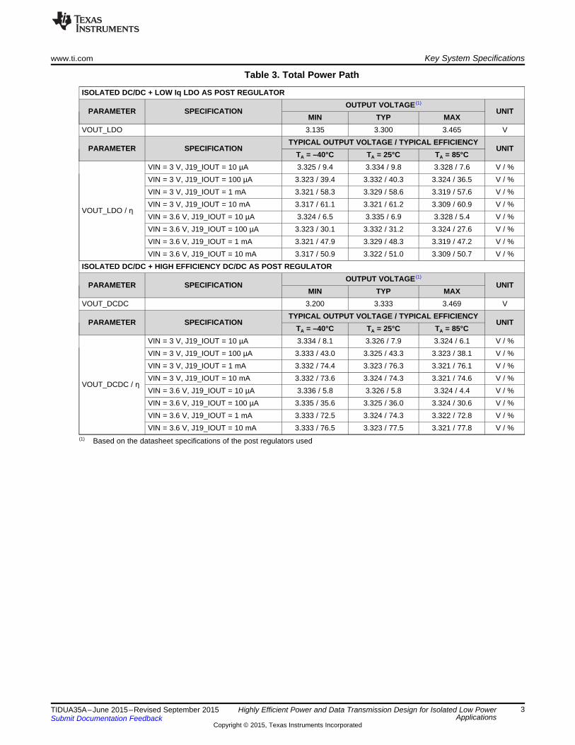
Table 3. Total Power Path
ISOLATED DC/DC + LOW Iq LDO AS POST REGULATOROUTPUT VOLTAGE (1)
PARAMETER SPECIFICATION UNITMIN TYP MAX
VOUT_LDO 3.135 3.300 3.465 VTYPICAL OUTPUT VOLTAGE / TYPICAL EFFICIENCY
PARAMETER SPECIFICATION UNITTA = –40°C TA = 25°C TA = 85°C
VIN = 3 V, J19_IOUT = 10 µA 3.325 / 9.4 3.334 / 9.8 3.328 / 7.6 V / %VIN = 3 V, J19_IOUT = 100 µA 3.323 / 39.4 3.332 / 40.3 3.324 / 36.5 V / %VIN = 3 V, J19_IOUT = 1 mA 3.321 / 58.3 3.329 / 58.6 3.319 / 57.6 V / %VIN = 3 V, J19_IOUT = 10 mA 3.317 / 61.1 3.321 / 61.2 3.309 / 60.9 V / %
VOUT_LDO / ηVIN = 3.6 V, J19_IOUT = 10 µA 3.324 / 6.5 3.335 / 6.9 3.328 / 5.4 V / %VIN = 3.6 V, J19_IOUT = 100 µA 3.323 / 30.1 3.332 / 31.2 3.324 / 27.6 V / %VIN = 3.6 V, J19_IOUT = 1 mA 3.321 / 47.9 3.329 / 48.3 3.319 / 47.2 V / %VIN = 3.6 V, J19_IOUT = 10 mA 3.317 / 50.9 3.322 / 51.0 3.309 / 50.7 V / %
ISOLATED DC/DC + HIGH EFFICIENCY DC/DC AS POST REGULATOROUTPUT VOLTAGE (1)
PARAMETER SPECIFICATION UNITMIN TYP MAX
VOUT_DCDC 3.200 3.333 3.469 VTYPICAL OUTPUT VOLTAGE / TYPICAL EFFICIENCY
PARAMETER SPECIFICATION UNITTA = –40°C TA = 25°C TA = 85°C
VIN = 3 V, J19_IOUT = 10 µA 3.334 / 8.1 3.326 / 7.9 3.324 / 6.1 V / %VIN = 3 V, J19_IOUT = 100 µA 3.333 / 43.0 3.325 / 43.3 3.323 / 38.1 V / %VIN = 3 V, J19_IOUT = 1 mA 3.332 / 74.4 3.323 / 76.3 3.321 / 76.1 V / %VIN = 3 V, J19_IOUT = 10 mA 3.332 / 73.6 3.324 / 74.3 3.321 / 74.6 V / %
VOUT_DCDC / ηVIN = 3.6 V, J19_IOUT = 10 µA 3.336 / 5.8 3.326 / 5.8 3.324 / 4.4 V / %VIN = 3.6 V, J19_IOUT = 100 µA 3.335 / 35.6 3.325 / 36.0 3.324 / 30.6 V / %VIN = 3.6 V, J19_IOUT = 1 mA 3.333 / 72.5 3.324 / 74.3 3.322 / 72.8 V / %VIN = 3.6 V, J19_IOUT = 10 mA 3.333 / 76.5 3.323 / 77.5 3.321 / 77.8 V / %
(1) Based on the datasheet specifications of the post regulators used
3TIDUA35A–June 2015–Revised September 2015 Highly Efficient Power and Data Transmission Design for Isolated Low PowerApplicationsSubmit Documentation Feedback
Copyright © 2015, Texas Instruments Incorporated

Key System Specifications www.ti.com
Table 4. Isolated DC/DC
PARAMETER COMMENTType of converter Half-bridge on primary, voltage doubler on secondaryLoop control Open-loop, optocoupler-lessTransformer insulation dielectric Functional, 1500-V AC 1 min, 1875-V AC 1 sec
VALUEPARAMETER SPECIFICATION UNIT
MIN TYP MAXVCC_IN Input voltage range 3.0 3.6 V
TYPICAL OUTPUT VOLTAGE / TYPICAL EFFICIENCYPARAMETER SPECIFICATION UNIT
TA = –40°C TA = 25°C TA = 85°CVIN = 3 V, J24_IOUT = 10 µA 5.6 / 16.0 5.8 / 18.5 5.5 / 12.7 V / %VIN = 3 V, J24_IOUT = 100 µA 4.8 / 58.5 5.0 / 63.0 5.2 / 59.6 V / %VIN = 3 V, J24_IOUT = 1 mA 4.6 / 81.4 4.8 / 85.1 5.0 / 86.9 V / %VIN = 3 V, J24_IOUT = 10 mA 4.1 / 75.4 4.2 / 77.3 4.2 / 78.0 V / %J24_VOUT /
ηIsolatedDC/DC VIN = 3.6 V, J24_IOUT = 10 µA 7.0 / 14.4 7.3 / 16.5 6.7 / 11.0 V / %VIN = 3.6 V, J24_IOUT = 100 µA 5.9 / 55.4 6.1 / 59.0 6.3 / 54.0 V / %VIN = 3.6 V, J24_IOUT = 1 mA 5.7 / 82.6 5.9 / 85.9 6.1 / 87.0 V / %VIN = 3.6 V, J24_IOUT = 10 mA 5.2 / 79.5 5.3 / 81.1 5.3 / 81.8 V / %
Table 5. Post Regulator
PARAMETER COMMENTType of post regulator Low Iq LDO or high efficiency DC/DC; selectable by jumperJ24_VIN Input voltage; equal to output voltage of isolated DC/DC (J24_VOUT)LOW Iq LDO
VALUE (1)
PARAMETER SPECIFICATION UNITMIN TYP MAX
VIN_operating Operating input voltage range 3.6 24 VIq Ground pin current 3.2 5.8 VVOUT Output voltage (VIN > 4.3 V) 3.135 3.3 3.465 V
Dropout voltage (IOUT = 10 mA;VDO 84 140 VVOUT = VOUT(NOM) – 0.1 V)η Efficiency See Section 7.1.5HIGH EFFICIENCY DC/DC
VALUE (1)
PARAMETER SPECIFICATION UNITMIN TYP MAX
VIN_operating Operating input voltage range 3 17 VVIN_startup VIN at which converter starts 4.122 4.32 4.535 VVIN_stop VIN at which converter stops 3.012 3.133 3.283 VVOUT Output voltage 3.2 3.333 3.469 Vη Efficiency See Section 7.1.4
(1) Based on the datasheet specifications of the post regulators used
4 Highly Efficient Power and Data Transmission Design for Isolated Low Power TIDUA35A–June 2015–Revised September 2015Applications Submit Documentation Feedback
Copyright © 2015, Texas Instruments Incorporated

Isolated DC/DC
8 to 33 V
Wide Input
Voltage
Sensor Element
AFE, ADC MCU MCU DAC
Analog or Digital
Interface
Pre-Regulator
TIDA-00459
GNDGND_iso
Highly Efficient Power and Data Transmission Design
for Isolated Low Power Applications
3.3 V
Post-Regulator
Half-BridgeDriver
Power
Isolation
GND
3.3 V
Analog /Digital
Data
GND_iso
Non-Isolated SideIsolated Side
Data
www.ti.com System Description
2 System DescriptionThe main purpose of this design is to provide a highly efficient low-power solution for avoiding groundloops in signal conditioning and bidirectional data transmission applications by providing isolation for thepower path as well as for the data transmission path.
Because ground potential differences are common in a large variety of different applications such asfactory automation, process control, building automation, energy harvesting and portable instrumentation,some sensors (like thermocouple sensors) and signal conditioning circuitry must be galvanically isolatedfrom the ground. In such isolated sensor transmitters, both the power supply and the data transmissionpath have to be isolated (Figure 1).
Figure 1. TIDA-00459 Used in Isolated Sensor Transmitter System
The data transmission path in such applications can be either unidirectional or bidirectional, of which thebidirectional is more challenging.
A bidirectional communication is needed in systems in which not only the isolated sensor side sends thedata, but also the host provides (for example, configuration data to the isolated sensor side). The mainchallenge of such a solution is the limited size within industry standard sensor transmitters and, in case ofa loop-powered system, the overall current consumption.
A single-wire interface is crucial to ensure space and power consumption constrains. In the realapplication, one MCU (placed on the isolated side) takes care of the signal conditioning (linearization,calibration, data acquisition routine) while the second MCU (placed on the non-isolated side) takes care ofthe communication (in case of HART or more complex communications than just 4 to 20 mA) and sendingdifferent configurations to the isolated sensor side.
The other challenge is related to the low power level of such applications, often ranging from tens ofmilliwatts down into the sub-milliwatt range. While solutions are already available for high efficiencyisolated DC/DC converters addressing an output power range above hundreds of milliwatts [1], therequired isolated power solution needs to be uniquely efficient even at much lower power levels aspreviously mentioned. A high power efficiency enables applications with limited input power or inputcurrent budgets such as loop powered 4- to 20-mA transmitters or bus powered applications where thebus power is limited.
5TIDUA35A–June 2015–Revised September 2015 Highly Efficient Power and Data Transmission Design for Isolated Low PowerApplicationsSubmit Documentation Feedback
Copyright © 2015, Texas Instruments Incorporated

System Description www.ti.com
Figure 1 shows a typical fully isolated sensor transmitter system where the TIDA-00459 is powered on thenon-isolated system side by a pre-regulated non-isolated 3.3-V rail. The TIDA-00459 is then used topower the signal conditioning and signal processing of the isolated side. The isolated rail generated by theTIDA-00459 is a well regulated isolated 3.3 V, eliminating the need for an additional 3.3-V post regulatoron the isolated side.
The galvanic isolation of the TIDA-00459 is transformer based and has an inherent life span advantageover an optocoupler isolator. Industrial devices typically operate for much longer periods of time thanconsumer electronics. Therefore, maintenance of effective isolation over a period of over 15 years isimportant. In systems requiring galvanic isolation between the transmitter and the receiver, the commonlyused coupling element are therefore transformers.
The TIDA-00459 provides functional isolation for the data transmission and power path between the non-isolated and the isolated system side. The design can also be used in similar applications where thefunctional isolation of the used transformers is sufficient. Other use cases may require modifiedtransformers to fulfill more stringent isolation requirements.
6 Highly Efficient Power and Data Transmission Design for Isolated Low Power TIDUA35A–June 2015–Revised September 2015Applications Submit Documentation Feedback
Copyright © 2015, Texas Instruments Incorporated

Post Regulators
Half-BridgeDriver
TPS60402
VoltageDoubler
2 x
Iso
lati
on
Isolated SideNon-Isolated Side
Low Iq LDO
TPS715A33
High Efficiency DC/DC
TPS62125
MCU
MSP430FR5969
MCU
MSP430FR5969
GND
GND GND_iso
J11
J15
J16J9
J19J24
J14
J13
J21
J20
S6 S5
S4D4 D5 D6 S1 D3 D2 D1
S2 S3
J17
J7
J23
J22
GND isoGND
J10
GND
DataTransformer
Power Transformer
VCC
3V to 3.6V
VCC / 2
J1 J4
VCC_iso
(+3.3V)
BoosterPack Interface
BoosterPack Interface
BoosterPack Interface
BoosterPack Interface
JTA
G In
terf
ace
JTA
G In
terf
ace
GND_iso
Pulse Former Pulse Former
J18
3.3V
3.3V
3 to 3.6-VExternal Power
3 to 3.6-VExternal Power
Isolated DC/DC
1 2
3
1 21 2 3
12
3
1 2
3
1 23
GND_iso
1
2
U3
U5
U4
U2
U1
2
1
1 2 3
2
1
2
1
21
T
T
T
T
T
www.ti.com Block Diagram
3 Block Diagram
Figure 2. TIDA-00459 Block Diagram
7TIDUA35A–June 2015–Revised September 2015 Highly Efficient Power and Data Transmission Design for Isolated Low PowerApplicationsSubmit Documentation Feedback
Copyright © 2015, Texas Instruments Incorporated

Block Diagram www.ti.com
Figure 2 shows the block diagram of the TIDA-00459. The design consists of:• the isolated bidirectional data transmission path• the isolated power path• the peripherals and interface components
The block diagram is split into the non-isolated and the isolated side, both separated from each other bythe isolation barrier. Each side has a dedicated ground (GND on the non-isolated side, GND_iso on theisolated side).
Isolated Bidirectional Data Transmission PathThis design provides a method for transmitting digital data bidirectional over an isolation boundary fromone MCU to another MCU using a single isolation component, a pulse transformer. The use of thetransformers to cross the isolation boundary is typical in industrial applications due to their robustness,low-power consumption, and low cost. The challenge of such a solution is first of all the limited size withinsensor transmitters (industry standard) and in case of a loop-powered system the overall currentconsumption.
For the MCUs, the MSP430FR5969 has been chosen because of its ULP system architecture, integratedcomparator, and integrated UART module, which is used for the isolated data transmission.
Isolated Power PathThe power path of the design spans from the header J7 on the non-isolated side to the header J19 on theisolated side. The input voltage on the non-isolated side is a 3.3-V rail, which can range from 3 to 3.6 Vand can be provided either by the JTAG interface (J10) or by the connector J18. The isolation barrier iscrossed by the power transformer of the isolated DC/DC. The isolated DC/DC is using a half-bridgetopology on the primary side and uses a voltage doubler on the secondary. The half bridge is running witha fixed frequency and with a fixed 50% duty cycle. It uses an open-loop control approach, which makesthe use of optocoupler needles. The design offers two different user-selectable post regulators on theisolated side: a low Iq LDO (U5) as well as a high efficiency DC/DC (U4). The selection of the postregulator is done by a simple jumper setting (J24, J19). The output voltage on the isolated side of thepower path is a regulated 3.3-V, which can be loaded with up to 10 mA. It is used to power the MCU (U1)on the isolated side. This isolated and regulated 3.3-V rail is brought out on the connector J11 and theBoosterPack connector J13 to power external circuits (sensor element, AFE, ADC, and so on) on theisolated side as shown in Figure 1.
Peripherals and Interface ComponentsTo showcase the functionality, the hardware of the TIDA-00459 includes BoosterPack connectors on bothsides of the isolation. BoosterPack plug-in modules allow the user to extend the functionality of thehardware and add features like wireless connectivity, capacitive touch, temperature sensing, displays, andmuch more (www.ti.com/boosterpack). The design files include design considerations, block diagrams,schematics, bill of materials (BOM), layer plots, Altium files, Gerber files, and MSP430™ firmware.
8 Highly Efficient Power and Data Transmission Design for Isolated Low Power TIDUA35A–June 2015–Revised September 2015Applications Submit Documentation Feedback
Copyright © 2015, Texas Instruments Incorporated

www.ti.com Block Diagram
3.1 Highlighted Products
3.1.1 MSP430FR5969The TIDA-00459 reference design uses the MSP430 ULP ferroelectric RAM (FRAM) platform. TheMSP430 combines a uniquely embedded FRAM and a holistic ULP system architecture, allowinginnovators to increase performance at lowered energy budgets. FRAM is much faster to write to than flashand has near infinite endurance, which means that in a remote sensor, data could be written more oftenfor improved data accuracy, or it could collect data for a longer period of time. Due to the lack of a chargepump, FRAM enables lower average and peak power during writes. Writing to FRAM does not require asetup sequence or additional power when compared to reading from FRAM. The FRAM read current isincluded in the active mode current consumption numbers already.
The bitwise programmable memory can be used at the programmer’s convenience for data or programstorage. It also does not require things like pre-erasure of segments before a write. Security is anotherarea where FRAM can offer advantages. FRAM is inherently more secure due to its makeup, and de-layering is not effective. FRAM is also resistant to alpha radiation and SER effects. There are two maindifferences between FRAM and static RAM (SRAM):• FRAM is nonvolatile; that is, it retains contents on loss of power.• The embedded FRAM on MSP430 devices can be accessed (read or write) at a maximum speed of
8 MHz.
In comparison to MSP430 flash, FRAM:• Is very easy to use• Requires no setup or preparation such as unlocking of control registers• Is not segmented and each bit is individually erasable, writable, and addressable• Does not require an erase before a write• Allows low-power write accesses (does not require a charge pump)• Can be written to across the full voltage range (1.8 to 3.6 V)• Can be written to at speeds close to 8MBps (maximum flash write speed including the erase time is
approximately 14 kBps)
Writing to FRAM does not require additional power when compared to reading from FRAM. The FRAMread current is included in the active mode current consumption numbers already. Table 6 summarizesthe FRAM advantages versus other memory technologies.
Table 6. FRAM Advantages
SPECIFICATION FRAM SRAM FLASHWrite speed per word 125 ns < 125 ns 85 us
Erase time No pre-erase required No pre-erase required 23 ms for 512 bytesBit-wise programmable Yes Yes No
Write endurance 1015 write per erase cycle N/A 1015 write per erase cycleNonvolatile Yes No Yes
Internal write voltage 1.5 V 1.5 V 12 to 14 V (charge pump required)
Features:• Embedded microcontroller
– 16-bit RISC architecture up to 16-MHz clock– Wide supply voltage range (1.8 to 3.6 V; Minimum supply voltage is restricted by SVS levels.)
• Optimized ULP modes– Active mode: Approximately 100 μA/MHz– Standby (LPM3 with VLO): 0.4 μA (typical)– Real-time clock (LPM3.5): 0.25 μA (typical; RTC is clocked by a 3.7-pF crystal.)– Shutdown (LPM4.5): 0.02 μA (typical)
9TIDUA35A–June 2015–Revised September 2015 Highly Efficient Power and Data Transmission Design for Isolated Low PowerApplicationsSubmit Documentation Feedback
Copyright © 2015, Texas Instruments Incorporated
Block Diagram www.ti.com
• ULP FRAM– Up to 64KB of nonvolatile memory– ULP writes– Fast write at 125 ns per word (64KB in 4 ms)– Unified memory = Program + Data + Storage in one single space– 1015 write cycle endurance– Radiation resistant and nonmagnetic
• Intelligent digital peripherals– 32-bit hardware multiplier (MPY)– Three-channel internal DMA– RTC with calendar and alarm functions– Five 16-bit timers with up to seven capture/compare registers each– 16-bit cyclic redundancy checker (CRC)
• High-performance analog– 16-channel analog comparator– 12-bit analog-to-digital converter (ADC) with internal reference and sample-and-hold and up to
16 external input channels• Multifunction I/O ports
– All pins support capacitive touch capability with no need for external components– Accessible bit-, byte-, and word-wise (in pairs)– Edge-selectable wake from LPM on all ports– Programmable pullup and pulldown on all ports
• Code security and encryption– 128-bit or 256-bit AES security encryption and decryption coprocessor– Random number seed for random number generation algorithms
• Enhanced serial communication– eUSCI_A0 and eUSCI_A1 support
• UART with automatic baud-rate detection• IrDA encode and decode• SPI at rates up to 10 Mbps
– eUSCI_B0 supports• I2C with multiple slave addressing• SPI at rates up to 8Mbps
– Hardware UART and I2C bootstrap loader (BSL)• Flexible clock system
– Fixed-frequency DCO with 10 selectable factory-trimmed frequencies– Low-power low-frequency internal clock source (VLO)– 32-kHz crystals (LFXT)– High-frequency crystals (HFXT)
• Development tools and software– Free professional development environments with EnergyTrace™++ technology development kit
(MSP-TS430RGZ48C)
For complete module descriptions, See the MSP430FR58xx, MSP430FR59xx, MSP430FR68xx, andMSP430FR69xx Family User's Guide (SLAU367).
10 Highly Efficient Power and Data Transmission Design for Isolated Low Power TIDUA35A–June 2015–Revised September 2015Applications Submit Documentation Feedback
Copyright © 2015, Texas Instruments Incorporated

EEM(S: 3 + 1)
RTC_A
Comp_E
(up to 16inputs)
FRAM
64KB48KB32KB
RAM
2KB1KB
PowerMgmt
LDOSVS
Brownout
SMCLK
ACLK
MDB
MAB
LFXOUT,HFXOUT
LFXIN,HFXIN
Spy-Bi-Wire
CRC16
BusControlLogic
MAB
MDB
MAB
MDB
MCLK
P1.x, P2.x
2x8
I/O PortPJ
1x8 I/Os
I/O PortsP3 4
2x8 I/Os
PB1x16 I/Os
, PI/O PortsP1, P2
2x8 I/Os
PA1x16 I/Os
P3.x, P4.x PJ.x
2 1x x8 8
MPY32
AES256
SecurityEnDecryption(128, 256)
cryption,
ADC12_B
(up to 16standardinputs,up to 8
differentialinputs)
ClockSystem
CPUXV2incl. 16
Registers
JTAG
Interface
DMA
Controller
3 Channel
Watchdog
REF_A
VoltageReference
MPUIP Encap
TB0
Timer_B7 CC
Registers(int, ext)
TA0
Timer_A3 CC
Registers(int, ext)
TA1
Timer_A3 CC
Registers(int, ext)
TA2TA3
Timer_A2 CC
Registers(int. only)
RTC_B
eUSCI_A0eUSCI_A1
(UART,IrDA,SPI)
eUSCI_B0
(I2C,SPI)
Capacitive Touch IO 0/1
LPM3.5 Domain
EnergyTrace++
www.ti.com Block Diagram
Figure 3. MSP430FR5969 Block Diagram
The MSP430 ULP FRAM portfolio consists of a diverse set of devices featuring FRAM, the ULP 16-bitMSP430 CPU, and intelligent peripherals targeted for various applications. The Comparator_E (COMP_E)and the eUSCI_A modules are used in this application.
The COMP_E module supports precision slope ADCs, supply voltage supervision, and monitoring ofexternal analog signals. Features of COMP_E include:• Inverting and non-inverting terminal input multiplexer• Software-selectable RC filter for the comparator output• Output provided to Timer_A capture input• Software control of the port input buffer• Interrupt capability• Selectable reference voltage generator and voltage hysteresis generator• Reference voltage input from shared reference• ULP comparator mode• Interrupt driven measurement system for low-power operation support
11TIDUA35A–June 2015–Revised September 2015 Highly Efficient Power and Data Transmission Design for Isolated Low PowerApplicationsSubmit Documentation Feedback
Copyright © 2015, Texas Instruments Incorporated

Block Diagram www.ti.com
The enhanced universal serial communication interface A (eUSCI_A) supports multiple serialcommunication modes with one hardware module. In this design, the UART mode is used. UART modefeatures include:• 7-bit or 8-bit data with odd, even, or non-parity• Independent transmit and receive shift registers• Separate transmit and receive buffer registers• LSB-first or MSB-first data transmit and receive• Built-in idle-line and address-bit communication protocols for multiprocessor systems• Receiver start-edge detection for auto wake up from LPMx modes (wake up from LPMx.5 is not
supported)• Programmable baud rate with modulation for fractional baud-rate support• Status flags for error detection and suppression• Status flags for address detection• Independent interrupt capability for receive, transmit, start bit received, and transmit complete
12 Highly Efficient Power and Data Transmission Design for Isolated Low Power TIDUA35A–June 2015–Revised September 2015Applications Submit Documentation Feedback
Copyright © 2015, Texas Instruments Incorporated

Start
FF
R
S
Q
VI – VCFLY+ < 0.5 V
VI
MEASVI < 1 V
VI
VO > Vbe
VO
MEAS
VO
OSC
OSCCHG
50 kHz
VO > –1 V
VI / VO
MEAS
VI VO
VCO_CONT
VO < –VI – Vbe
Phase
Generator
DC_ Startup
C(fly)
+
Q3Q2
Q1
Q4
VI
VO
GND
Q5
Q
QB
DC_ Startup
www.ti.com Block Diagram
3.1.2 TPS60402The TPS60402 [6] is used in a modified way to drive the power transformer T2 of the open loop isolatedDC/DC in this TIDA-00459 reference design. The device was selected due to its integrated FETs whichare sized for such low power application and which are usable as half-bridge driver. The TPS60402comes furthermore with an internal oscillator generating the complementary 50% duty cycle control signalfor the half-bridge FETs (Q1 and Q2) as illustrated in Figure 4. Finally, the device features a low quiescentcurrent, which is mandatory to use in this design.
Figure 4. TPS60400 Family—Functional Block Diagram
The primary applicable and beneficial specifications of the TPS60400 device family can be summarized asfollows:• Input voltage range from 1.6 to 5.5 V• Small 5-pin SOT23 package• Integrated switches (FETs)• Internal fixed frequency oscillator (for TPS60401 to TPS60403)• Multiple switching frequency versions, as shown in Table 7• Devices available with quiescent current down to 65 μA
Table 7. TPS60400 Family—Device Versions
PARAMETER TPS60400 TPS60401 TPS60402 TPS60403Variable switching frequencySwitching frequency (typ) 20 kHz 50 kHz 250 kHz50 to 250 kHz
Quiescent current (typ) 125 µA 65 µA 120 µA 425 µA
The TPS60402 was selected from the TPS60400 family. With a 50-kHz switching frequency, theTPS60402 offers a good trade-off between efficiency and solution size.
13TIDUA35A–June 2015–Revised September 2015 Highly Efficient Power and Data Transmission Design for Isolated Low PowerApplicationsSubmit Documentation Feedback
Copyright © 2015, Texas Instruments Incorporated

_ +
Current
Sense Leakage Null
Control CircuitR1
R2
V(IN)
GND
V(OUT)
ILIM
Bandgap
Reference
V = 1.205 Vref
TPS715A33
IN OUTVIN
VOUT
C1
0.1 mF0.47 mF
GND
Block Diagram www.ti.com
3.1.3 TPS715A33The TPS715A33 [2] is an low Iq LDO, used as one of the two user selectable post regulators, generatinga well regulated 3.3-V rail from the open-loop, isolated DC/DC’s non-regulated output. An LDO-based postregulator is by far the simplest, less complex, and the most cost effective approach for doing the requiredpost regulation. The specific device was selected due to its wide input voltage range, its low and loadindependent quiescent current (Iq), and the fact that the accuracy of its output voltage is specified down to0 mA. The fixed 3.3-V output voltage version was chosen to simplify the design and to eliminate theadditional tolerances and temperature drift of the external voltage setting resistors otherwise needed whenthe adjustable version would have been used (see Figure 5 and Figure 6).
Figure 5. Typical Application Circuit Figure 6. Functional Block Diagram(Fixed-Voltage Version) (Fixed Version)
The TPS715A low-dropout voltage regulators (LDO) offer the benefits of high input voltage, low-dropoutvoltage, low-power operation, and miniaturized packaging. The devices, which operate over an inputrange of 2.5 to 24 V, are stable with any capacitor (> 0.47 μF). The high maximum input voltage combinedwith excellent power dissipation capability makes this part particularly well-suited to industrial andautomotive applications. A PMOS pass element behaves as a low-value resistor. The low-dropout voltage,typically 670 mV at 80 mA of load current, is directly proportional to the load current. The low quiescentcurrent (3.2 μA typically) is nearly constant over the entire range of output load current (0 to 80 mA). TheTPS715A is available in 3×3-mm package ideal for high power dissipation and small 2×2-mm packageideal for handheld and ultra-portable applications. The 3×3-mm package is also available as a non-magnetic package for medical imaging applications.
Features:• 24-V maximum input voltage• Low 3.2-μA quiescent current at 80 mA• Stable with any capacitor (≥ 0.47 μF)• 80-mA specified current• Available in fixed and adjustable (1.2 to 15 V) versions• Specified current limit• 3×3-mm and 2×2-mm SON packages• –40°C to 125°C specified junction temperature range
14 Highly Efficient Power and Data Transmission Design for Isolated Low Power TIDUA35A–June 2015–Revised September 2015Applications Submit Documentation Feedback
Copyright © 2015, Texas Instruments Incorporated
50
55
60
65
70
75
80
85
90
95
100
0.01 0.1 1 10 100 1000
Output Current (mA)
Effic
iency (
%)
VIN = 4.0V
VIN = 5V
VIN = 7.5V
VIN = 9V
VIN = 12V
VIN = 15V
V = 3.3V
L = 15 H VLF302515
C = 10µF
OUT
OUT
µ
VIN
FB
TPS62125
PG
L 15 HµSW
C
10OUT
µFCurrentSource0.5mA10V max
GND
R1
R2
VOS
C
10IN
Fµ
Rpullup
PWR Good
EN_hys
EN
576k
1.8MREN1
R2
110k
610k
REN2
REN_hys
120k
C
22IN
FPoscap
µ
100k
V = 3.3V
up to 300mAOUTV = 6.82VIN_Start
V = 4.55VIN_Stop
www.ti.com Block Diagram
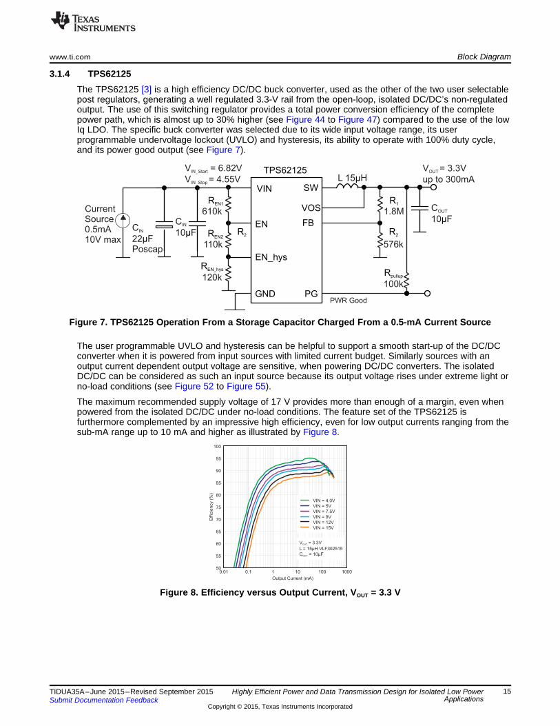
3.1.4 TPS62125The TPS62125 [3] is a high efficiency DC/DC buck converter, used as the other of the two user selectablepost regulators, generating a well regulated 3.3-V rail from the open-loop, isolated DC/DC’s non-regulatedoutput. The use of this switching regulator provides a total power conversion efficiency of the completepower path, which is almost up to 30% higher (see Figure 44 to Figure 47) compared to the use of the lowIq LDO. The specific buck converter was selected due to its wide input voltage range, its userprogrammable undervoltage lockout (UVLO) and hysteresis, its ability to operate with 100% duty cycle,and its power good output (see Figure 7).
Figure 7. TPS62125 Operation From a Storage Capacitor Charged From a 0.5-mA Current Source
The user programmable UVLO and hysteresis can be helpful to support a smooth start-up of the DC/DCconverter when it is powered from input sources with limited current budget. Similarly sources with anoutput current dependent output voltage are sensitive, when powering DC/DC converters. The isolatedDC/DC can be considered as such an input source because its output voltage rises under extreme light orno-load conditions (see Figure 52 to Figure 55).
The maximum recommended supply voltage of 17 V provides more than enough of a margin, even whenpowered from the isolated DC/DC under no-load conditions. The feature set of the TPS62125 isfurthermore complemented by an impressive high efficiency, even for low output currents ranging from thesub-mA range up to 10 mA and higher as illustrated by Figure 8.
Figure 8. Efficiency versus Output Current, VOUT = 3.3 V
15TIDUA35A–June 2015–Revised September 2015 Highly Efficient Power and Data Transmission Design for Isolated Low PowerApplicationsSubmit Documentation Feedback
Copyright © 2015, Texas Instruments Incorporated

Block Diagram www.ti.com
The TPS62125 is a high efficiency synchronous step-down converter optimized for low and ultra-lowpower applications providing up to a 300-mA output current. The wide input voltage range of 3 to 17-Vsupports four cell alkaline and 1- to 4-cell Li-Ion batteries in series configuration as well as 9-V to 15-Vpowered applications. The device includes a precise low-power enable comparator that can be used as aninput supply voltage supervisor (SVS) to address system specific power up and down requirements. Theenable comparator consumes only 6-μA quiescent current and features an accurate threshold of 1.2 Vtypical as well as an adjustable hysteresis. With this feature, the converter can generate a power supplyrail by extracting energy from a storage capacitor fed from high impedance sources such as solar panelsor current loops. With its DCS-Control™ scheme the converter provides power save mode operation tomaintain highest efficiency over the entire load current range. At light loads, the converter operates inPFM mode (pulse frequency modulation) and transitions seamlessly and automatically in pulse widthmodulation (PWM) mode at higher load currents. The DCS-Control scheme is optimized for low outputripple voltage in PFM mode in order to reduce output noise to a minimum and features excellent AC loadregulation. An open drain power good output indicates once the output voltage is in regulation.
Features:• Wide input voltage range: 3 to 17 V• Input SVS with adjustable threshold / hysteresis• Wide output voltage range: 1.2 to 10 V• Typical 13-μA quiescent current• 350-nA typical shutdown current• Seamless power save mode transition• DCS-Control scheme• Low output ripple voltage• Up to 1-MHz switching frequency• Highest efficiency over wide VIN and VOUT range• 100% duty cycle mode• Power good open drain output• Output discharge function• Small 2×2-mm2 SON 8-pin package
16 Highly Efficient Power and Data Transmission Design for Isolated Low Power TIDUA35A–June 2015–Revised September 2015Applications Submit Documentation Feedback
Copyright © 2015, Texas Instruments Incorporated
MSP430FR5969 MSP430FR5969
COUT
eUSCI_AeUSCI_A
MUX
MUXC2
COUT/C1
+
± C2COUT
+
±
RX
VCC/2 Vref0/Vref1
C1/COUT
TX TX
RX
TX/RX RX/TX
Isol
atio
n
t t
www.ti.com System Design Theory
4 System Design Theory
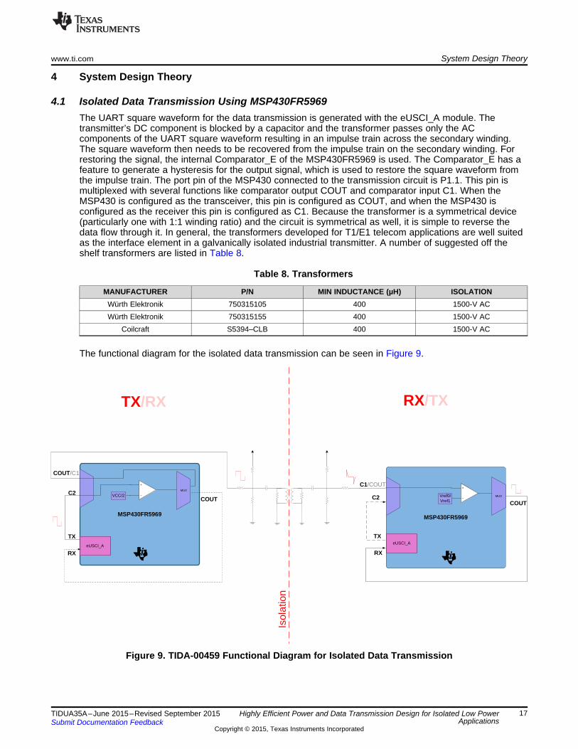
4.1 Isolated Data Transmission Using MSP430FR5969The UART square waveform for the data transmission is generated with the eUSCI_A module. Thetransmitter’s DC component is blocked by a capacitor and the transformer passes only the ACcomponents of the UART square waveform resulting in an impulse train across the secondary winding.The square waveform then needs to be recovered from the impulse train on the secondary winding. Forrestoring the signal, the internal Comparator_E of the MSP430FR5969 is used. The Comparator_E has afeature to generate a hysteresis for the output signal, which is used to restore the square waveform fromthe impulse train. The port pin of the MSP430 connected to the transmission circuit is P1.1. This pin ismultiplexed with several functions like comparator output COUT and comparator input C1. When theMSP430 is configured as the transceiver, this pin is configured as COUT, and when the MSP430 isconfigured as the receiver this pin is configured as C1. Because the transformer is a symmetrical device(particularly one with 1:1 winding ratio) and the circuit is symmetrical as well, it is simple to reverse thedata flow through it. In general, the transformers developed for T1/E1 telecom applications are well suitedas the interface element in a galvanically isolated industrial transmitter. A number of suggested off theshelf transformers are listed in Table 8.
Table 8. Transformers
MANUFACTURER P/N MIN INDUCTANCE (µH) ISOLATIONWürth Elektronik 750315105 400 1500-V ACWürth Elektronik 750315155 400 1500-V AC
Coilcraft S5394–CLB 400 1500-V AC
The functional diagram for the isolated data transmission can be seen in Figure 9.
Figure 9. TIDA-00459 Functional Diagram for Isolated Data Transmission
17TIDUA35A–June 2015–Revised September 2015 Highly Efficient Power and Data Transmission Design for Isolated Low PowerApplicationsSubmit Documentation Feedback
Copyright © 2015, Texas Instruments Incorporated

MSP430FR5969
eUSCI_A
MUX
COUT
+
±Vref0/Vref1
C1/COUT
RX
TX RXIs
olat
ion
R2
R8
R4C2
R7
t
System Design Theory www.ti.com
4.1.1 Receiving DataIf the MSP430 is in receiving mode, the P1.1 pin connected to the transmission circuit is configured ascomparator input C1. The comparator output COUT is mapped to a different pin P3.5, which is externallyconnected to the UART RX pin (see Figure 10).
Figure 10. Receiving Block Diagram
18 Highly Efficient Power and Data Transmission Design for Isolated Low Power TIDUA35A–June 2015–Revised September 2015Applications Submit Documentation Feedback
Copyright © 2015, Texas Instruments Incorporated
www.ti.com System Design Theory
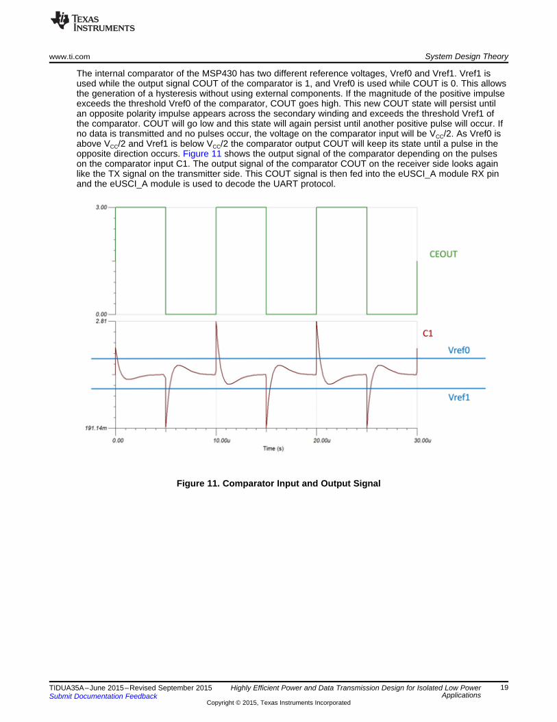
The internal comparator of the MSP430 has two different reference voltages, Vref0 and Vref1. Vref1 isused while the output signal COUT of the comparator is 1, and Vref0 is used while COUT is 0. This allowsthe generation of a hysteresis without using external components. If the magnitude of the positive impulseexceeds the threshold Vref0 of the comparator, COUT goes high. This new COUT state will persist untilan opposite polarity impulse appears across the secondary winding and exceeds the threshold Vref1 ofthe comparator. COUT will go low and this state will again persist until another positive pulse will occur. Ifno data is transmitted and no pulses occur, the voltage on the comparator input will be VCC/2. As Vref0 isabove VCC/2 and Vref1 is below VCC/2 the comparator output COUT will keep its state until a pulse in theopposite direction occurs. Figure 11 shows the output signal of the comparator depending on the pulseson the comparator input C1. The output signal of the comparator COUT on the receiver side looks againlike the TX signal on the transmitter side. This COUT signal is then fed into the eUSCI_A module RX pinand the eUSCI_A module is used to decode the UART protocol.
Figure 11. Comparator Input and Output Signal
19TIDUA35A–June 2015–Revised September 2015 Highly Efficient Power and Data Transmission Design for Isolated Low PowerApplicationsSubmit Documentation Feedback
Copyright © 2015, Texas Instruments Incorporated

RX TX
Isol
atio
n
MSP430FR5969
eUSCI_A
MUX
C2
COUT/C1
+
±VCC/2
TX
t
System Design Theory www.ti.com
4.1.2 Sending DataIn this circuit, the default VCC level on the connected MCU pin is VCC/2 when no data is transmitted. Thisis necessary to have the negative pulses not be going below 0 V as the I/O pins of the MSP430 do notaccept negative voltage. But when voltage levels around VCC / 2 are applied to digital CMOS gates,parasitic current can flow from VCC to GND inside the pin. This parasitic current occurs if the input voltageis near the transition level of the gate. As the TX pin of the eUSCI module is a digital CMOS gate, itshould not be directly connected to the transmission circuitry as parasitic current would flow from VCC toGND inside the pin. But on the P1.1/COUT/C1 pin, the port pin buffer can be disabled and this eliminatesthe parasitic current flow. Therefore, P1.1/COUT/C1 pin is connected to the transmission circuit. Fortransmitting, P1.1 is configured as comparator output COUT and the TX signal of the eUSCI module isconnected to the comparator input pin C2 (see Figure 12). The inverting input of the comparator isconnected to VCC/2 as a reference and the comparator output signal COUT then follows directly the TXsignal on pin C2. To transmit data, the eUSCI_A module is used in UART mode. The transmitter’s DCcomponent is blocked by a capacitor and only the AC components of the TX square waveform are passedto the secondary winding of the transformer.
Figure 12. Transmitting Block Diagram
20 Highly Efficient Power and Data Transmission Design for Isolated Low Power TIDUA35A–June 2015–Revised September 2015Applications Submit Documentation Feedback
Copyright © 2015, Texas Instruments Incorporated

www.ti.com System Design Theory
When one side of the MSP430FR5969 isolation is configured for RX and the other MSP430FR5969 on theother side is configured for TX, data transmission in one direction can be done continuously without anydelay (see Figure 13). The turquoise signal is the transmitted data, and the green signal is the receivedsignal on the other side of the isolation.
Figure 13. Transmitting Data
21TIDUA35A–June 2015–Revised September 2015 Highly Efficient Power and Data Transmission Design for Isolated Low PowerApplicationsSubmit Documentation Feedback
Copyright © 2015, Texas Instruments Incorporated
System Design Theory www.ti.com
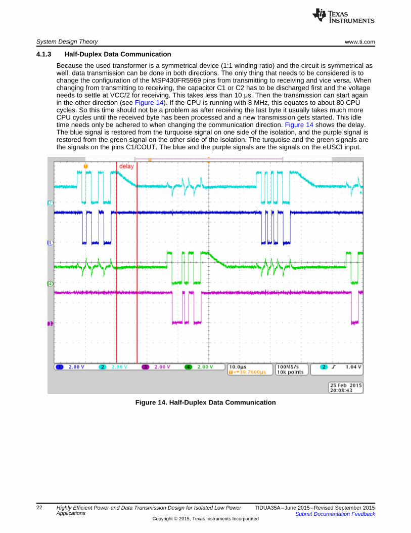
4.1.3 Half-Duplex Data CommunicationBecause the used transformer is a symmetrical device (1:1 winding ratio) and the circuit is symmetrical aswell, data transmission can be done in both directions. The only thing that needs to be considered is tochange the configuration of the MSP430FR5969 pins from transmitting to receiving and vice versa. Whenchanging from transmitting to receiving, the capacitor C1 or C2 has to be discharged first and the voltageneeds to settle at VCC/2 for receiving. This takes less than 10 μs. Then the transmission can start againin the other direction (see Figure 14). If the CPU is running with 8 MHz, this equates to about 80 CPUcycles. So this time should not be a problem as after receiving the last byte it usually takes much moreCPU cycles until the received byte has been processed and a new transmission gets started. This idletime needs only be adhered to when changing the communication direction. Figure 14 shows the delay.The blue signal is restored from the turquoise signal on one side of the isolation, and the purple signal isrestored from the green signal on the other side of the isolation. The turquoise and the green signals arethe signals on the pins C1/COUT. The blue and the purple signals are the signals on the eUSCI input.
Figure 14. Half-Duplex Data Communication
22 Highly Efficient Power and Data Transmission Design for Isolated Low Power TIDUA35A–June 2015–Revised September 2015Applications Submit Documentation Feedback
Copyright © 2015, Texas Instruments Incorporated

Synch
Start
Bit
Stop
Bit0 1 2 3 4 5 6 7
8 Bit Times
Break Delimiter Synch
www.ti.com System Design Theory
4.1.4 Automated Baud-Rate Detection and Break and Synch Sequence FeatureThe automatic baud-rate (ABR) detection feature of the eUSCI module allows matching of baud ratesbetween the different isolations sides. For ABR detection, a data frame is preceded by a synchronizationsequence that consists of a break and a synch field. A break is detected when 11 or more continuouszeros (spaces) are received. If the length of the break exceeds 21 bit times, the break timeout error flagUCBTOE is set. The synch field follows the break as shown in Figure 15.
Figure 15. ABR Detection—Break/Synch Sequence
The synch field consists of the data 055h inside a byte field (see Figure 16). The synchronization is basedon the time measurement between the first and the last falling edge of the pattern. The result of themeasurement is transferred into the baud-rate control registers.
Figure 16. ABR Detection—Synch Field
The break field can be used to detect the beginning of a new frame. The UCDORM bit is used to controldata reception in this mode. When UCDORM is set, all characters are received but not transferred into theeUSCI receive buffer UCA0RXBUF, and interrupts are not generated. When UCDORM is set, in UARTmode with ABR detection, only the combination of a break and synch field sets the UCRXIFG. When abreak/synch field is detected, the character following the break/synch field is transferred into UCA0RXBUFand the UCRXIFG interrupt flag is set. When a break/synch field is received, user software must resetUCDORM to continue receiving data. If UCDORM remains set, only the character after the next receptionof a break/synch field is received. This feature can make the communication really robust in noisyenvironments. In addition the MSP430FR5969 includes a hardware CRC module (CRC16). The CRC16produces a signature based on a sequence of entered data values and can be used for data checkingpurposes. The CRC16 module signature is based on the CRC-CCITT standard.
23TIDUA35A–June 2015–Revised September 2015 Highly Efficient Power and Data Transmission Design for Isolated Low PowerApplicationsSubmit Documentation Feedback
Copyright © 2015, Texas Instruments Incorporated

System Design Theory www.ti.com
Figure 17 shows a scope screenshot of the communication using the ABR Detection and Break/SynchSequence Feature followed by one data byte.
Figure 17. ABR Detection — Break/Synch Sequence Plus One Data Byte
24 Highly Efficient Power and Data Transmission Design for Isolated Low Power TIDUA35A–June 2015–Revised September 2015Applications Submit Documentation Feedback
Copyright © 2015, Texas Instruments Incorporated

MSP430F5172 MSP430F5172
COUT
eUSCI_AeUSCI_A
MUX
MUX
TX/C1+
±
COUT
+
±
RX
Vref0/Vref1
C1/TX
TX TX
RX
TX/RX RX/TX
Isol
atio
n
Vref0/Vref1
t t
www.ti.com System Design Theory
4.2 Isolated Data Transmission Using an MSP430 With Port Mapping FunctionalityThe port mapping controller allows the flexible and reconfigurable mapping of digital functions to port pins.The port mapping is configured with user software. If an MSP430 with port mapping functionality (forexample, MSP430F5172) is used for the isolated data transmission, the TX function of the eUSCI modulecan be directly mapped to the same pin as the comparator input C1. This makes the half-duplex datatransmission easier as the comparator is only needed for receiving data. (see Figure 18).
Figure 18. Isolated Data Transmission With MSP430F5172
25TIDUA35A–June 2015–Revised September 2015 Highly Efficient Power and Data Transmission Design for Isolated Low PowerApplicationsSubmit Documentation Feedback
Copyright © 2015, Texas Instruments Incorporated
GND
VCC_IN (3 to 3.6 V)
Con
trol
Lo
gic
TPS60402
GND_iso
VOUT_isoDCDC
C224.7�F
C2610�F
C2510�F
C244.7�F
C194.7�F
D8
D7
C216.8�F
T2C1822�F
VCC_IN / 2
n = 1 : 1.8
> 2.5mH
U3
VP VS VC19
VF_D7
VC24
VF_D8
VC21 = VOUT
VIN
F_DV2n
VINu�VOUT §
VF_'�§�VF_D7 §�9)_D8 at 2 x IOUT
SW 1(SWITCH-NODE 1)
GND
IN
CFLY+
GND
IOUT
Q1
Q2
System Design Theory www.ti.com
4.3 Isolated Power ConversionAs outlined in Section 3, the complete power path consists of the isolated DC/DC converter and twodifferent post regulators. The post regulator to be used can be selected by the user.
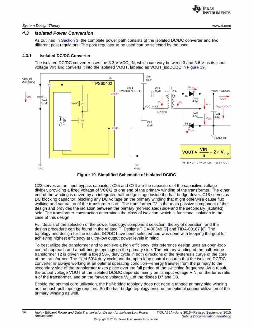
4.3.1 Isolated DC/DC ConverterThe isolated DC/DC converter uses the 3.3-V VCC_IN, which can vary between 3 and 3.6 V as its inputvoltage VIN and converts it into the isolated VOUT, labeled as VOUT_isoDCDC in Figure 19.
Figure 19. Simplified Schematic of Isolated DC/DC
C22 serves as an input bypass capacitor. C25 and C26 are the capacitors of the capacitive voltagedivider, providing a fixed voltage of VCC/2 to one end of the primary winding of the transformer. The otherend of the winding is driven by an integrated half-bridge stage inside the half-bridge driver. C18 serves asDC blocking capacitor, blocking any DC voltage on the primary winding that might otherwise cause fluxwalking and saturation of the transformer core. The transformer T2 is the main passive component of thedesign and provides the isolation between the primary (non-isolated) side and the secondary (isolated)side. The transformer construction determines the class of isolation, which is functional isolation in thecase of this design.
Full details of the selection of the power topology, component selection, theory of operation, and thedesign procedure can be found in the related TI Designs TIDA-00349 [7] and TIDA-00167 [8]. Thetopology and design for the isolated DC/DC have been selected and was done with keeping the goal forachieving highest efficiency at ultra-low output power levels in mind.
To best utilize the transformer and to achieve a high efficiency, this reference design uses an open-loopcontrol approach and a half-bridge topology on the primary side. The primary winding of the half-bridgetransformer T2 is driven with a fixed 50% duty cycle in both directions of the hysteresis curve of the coreof the transformer. The fixed 50% duty cycle and the open-loop control ensures that the isolated DC/DCconverter is always working at an optimal operating condition—energy transfer from the primary to thesecondary side of the transformer takes place over the full period of the switching frequency. As a result,the output voltage VOUT of the isolated DC/DC depends mainly on its input voltage VIN, on the turns ration of the transformer, and on the forward voltage VF_D of the diodes D7 and D8.
Beside the optimal core utilization, the half-bridge topology does not need a tapped primary side windingas the push-pull topology requires. So the half-bridge topology ensures an optimal copper utilization of theprimary winding as well.
26 Highly Efficient Power and Data Transmission Design for Isolated Low Power TIDUA35A–June 2015–Revised September 2015Applications Submit Documentation Feedback
Copyright © 2015, Texas Instruments Incorporated

Np NsVp Vs
IsIp
Np NsVNp Vs
ISIm
LL
Lm
RIp
VpVLm
IS‘
Ideal Transformer Simplified Model of Real Transformer
www.ti.com System Design Theory
To further keep the goal of getting a maximum efficiency at the ultra-low power levels, all losses need tobe minimized. The quiescent current of almost all ICs with integrated power MOSFETs targeted for low-power isolated DC/DC converters is too high (hundreds of microamps up to milliamps) to finally provide ahigh enough efficiency. Even worse, in most cases the quiescent current is specified with the devices noteven switching. As soon as they start switching, their switching losses will raise or lower the efficiencysignificantly—the higher the switching frequency, the higher the switching losses will be (which lowers theefficiency). Therefore, switching frequencies in the range of tens of kilohertz are better suited than usinghundreds of kilohertz.
While a low switching frequency reduces the switching losses, another challenge appears as outlined ingreater detail in Section 5.3 of the TIDA-00349 reference design [7]: The primary winding of thetransformer, which represents the magnetizing inductance Lm, sees almost the full primary voltageVLm ≈ VP, which is applied for a relatively long time when operated at a low switching frequency. This leadsto a high ∫VLmdt, also called the V-s product. The transformer used in the isolated DC/DC needs towithstand this V-s product without going into saturation. This is best demonstrated in Figure 21.
The gray hysteresis curve in Figure 21 is also known as the B-H curve and is used to characterize thecore material of the transformer itself. The slope of the curve represents the permeability, μ in this case.Applying the "Transformation of Axes" as described in Section 1 of the Magnetics Design Handbook [9],the vertical axis can also be used for the V-s applied to a specific inductor when the horizontal axis isused for the current flowing through this specific inductor. This specific inductor is in this case themagnetizing inductance Lm of the transformer and is then represented by the slope of the hysteresis curveas well. The horizontal axis is then specifically showing the magnetizing current Im. The blue curvebetween A and A' represents the so-called minor loop that is the practical range of excursion used in realapplications.
If the applied V-s product (or the flux-density B) violates a certain limit (the red dotted lines), then theslope changes from a linear to a nonlinear behavior. Any further increase in the applied V-s will cause adrastic increase of the magnetizing current. The inductive characteristic diminishes, leaving finally only thecopper resistance of the winding. A drastic increase of the magnetizing current also causes shorting of theprimary side of the ideal transformer block used in the simplified model of the real transformer (Figure 20).
Figure 20. Ideal Transformer versus Simplified Model of Real Transformer
Any voltage applied to the magnetizing inductance can cause such an effect, no matter how small. Thequestion is just how long the voltage is applied. This information explains why transformers can work forAC signals, but not for DC signals.
Even AC signals can cause this effect if the AC signals violate the V-s limit of the specific inductor. Such aviolation can happen, if the magnitude of the voltage is too large or the time the voltage is applied is toolong (for example, when operated at low frequency). The violation can also happen if the AC signal has aDC voltage superimposed. To avoid this situation, the V-s applied to an inductor (or the flux in the core)needs to be balanced. Therefore, any positive V-s excursion in one direction needs to be cancelled out byexactly the same excursion in the opposite direction. Otherwise, flux walking can happen driving the coreearlier or later into saturation.
27TIDUA35A–June 2015–Revised September 2015 Highly Efficient Power and Data Transmission Design for Isolated Low PowerApplicationsSubmit Documentation Feedback
Copyright © 2015, Texas Instruments Incorporated

��9Lmdt
H
B
Im
Slope of Hysteresis Curve Represents
�� Lm
V-s LimitViolated
A
$¶
or
or
V-s LimitViolated
or
System Design Theory www.ti.com
By adding a DC blocking capacitor (C18 in Figure 19), a potential flux walking can be addressed andavoided effectively in a half-bridge topology—a significant advantage compared to the push-pull.
Figure 21. Hysteresis Curve of Ferrite and Specific Inductor
The applied V-s product can be reduced only by reducing the ON-time tON of the integrated switches or thevoltage VLm respectively VP applied to the magnetizing inductance. The ON-time is determined by theswitching frequency and equals to almost 50% of the switching period and the applied voltage VP isdetermined by the input voltage VCC_IN. The use of the half-bridge topology to drive the transformerexcels the push-pull in respect of the applied voltage VP as well: it drives the primary winding with one halfof VCC_IN only instead of the full voltage, which is applied in case of a push-pull. This reduces theneeded V-s capability of the transformer used in a half-bridge configuration to one half compared to apush-pull operated with the same switching frequency.
On the other side, providing only half the VCC_IN to the primary winding of transformer T2 will transferonly half of the voltage to the secondary winding. This can be compensated by adapting the turns ratio nof the transformer or by the used rectifier topology on the secondary side.
Because the output voltage of the isolated DC/DC needs to incorporate enough headroom for thefollowing 3.3-V post regulators, an additional boost of that output voltage is required. Using solely themodification of the turns ratio of the transformer to achieve this boost and to compensate for driving theprimary winding of the transformer with only VCC_IN / 2 might complicate the transformer design more.More number of turns and even additional layers on the secondary would be required, increasing thecopper resistance of the winding and making the coupling and capacity between primary and secondaryworse.
Therefore, the design uses a voltage doubler topology for the rectification on the secondary side tocompensate for the half-voltage drive on the primary. The voltage doubler consists of D7, D8, C19, andC24. The modification of the transformers turns ratio is used to address the need for the post regulators’headroom voltage as well as for the compensation of the forward voltage drops in the diodes and theother losses in the parasitic elements of the circuit. In the special case of this design, the primary-to-secondary side turns ratio n was chosen to be 1:1.8, resulting in enough headroom voltage to enable bothpost regulators to operate with their full dynamic performance under all load and temperature conditions.
28 Highly Efficient Power and Data Transmission Design for Isolated Low Power TIDUA35A–June 2015–Revised September 2015Applications Submit Documentation Feedback
Copyright © 2015, Texas Instruments Incorporated

FRM_DI 2 IOUT> ´
( )F AVI IOUT=
D F _DVR VOUT _ isoDCDC V= +
F _D
VCC _INVOUT _ isoDCDC 2 V
n= - ´
www.ti.com System Design Theory
4.3.1.1 Isolated DC/DC Converter—Design EquationsThis section presents the design equations for selecting the transformer and the diodes of the isolatedDC/DC converter. Adequate margins have to be factored in when selecting the components and valuesneeds to be confirmed by real measurements to see the effects of parasitics and non-ideal circuit behaviorand to adapt the circuit and components selection accordingly. Additional details can be found in therespective section of the TIDA-00349 reference design [7].
The basic voltage conversion of the isolated DC/DC converter is described by Equation 1. It outlines veryclearly the dependency of the output voltage on the input voltage of the isolated DC/DC converter. Thediodes’ forward voltage is one of the main contributor of losses as well as of the dependency of the outputvoltage on the output current and temperature. All those dependencies are a typical characteristic of anyopen loop converter not incorporating a control mechanism.
space
(1)
where• VOUT_isoDCDC is the output voltage of the isolated DC/DC• VCC_IN is the input voltage of the isolated DC/DC• VF_D is the forward voltage drop of each diode D7 and D8 at twice the output current IOUT of the
isolated DC/DC• n is the primary-to-secondary turns ratio of transformer T2
NOTE: This is only one possible way to define the turns ratio. Some literature or transformermanufacturer define the turns ratio to the exact contrary as a secondary-to-primary turnsratio.
The diodes D7 and D8 need to be selected by their reverse voltage, average, and repetitive forwardcurrent. Their forward voltage, reverse current, diode capacitance, and reverse recovery times should beas small as possible to maximize efficiency. When deciding, consider their behavior at temperatureextremes.
space
(2)
where• VRD is the minimum required reverse voltage of each of the diodes D7 and D8
space
(3)
where• IF(AV) is the minimum required average forward current of each diodes D7 and D8
space
(4)
where• IFRM_D is the minimum required repetitive peak forward current of each of the diodes D7 and D8.
29TIDUA35A–June 2015–Revised September 2015 Highly Efficient Power and Data Transmission Design for Isolated Low PowerApplicationsSubmit Documentation Feedback
Copyright © 2015, Texas Instruments Incorporated

VCC _IN_maxVt
4 f _min>
´
F _D _ max_ T _ min
VCC _IN_minn
VOUT _ isoDCDC _min 2 V=
+ ´
System Design Theory www.ti.com
Re-arranging Equation 1 and knowing the diodes’ forward voltages at the respective current levels allowsthe calculation of the needed turns ratio for the transformer. Considering the worst case condition,Equation 1 can be re-arranged to
space
(5)
where• VOUT_isoDCDC_min is the minimum output voltage of the isolated DC/DC needed to ensure proper
operation of the post regulators• VCC_IN_min is the minimum available input voltage of the isolated DC/DC• VF_D_max_T_min is the maximum forward voltage drop at the minimum temperature of each of the diodes
D7 and D8 at twice the output current IOUT of the isolated DC/DC• n is the primary-to-secondary turns ratio of transformer T2
To avoid saturation of the transformer, the transformer must be able to withstand the maximum V-sproduct, which can happen in the design.
space
(6)
where• Vt is the V-s product the transformer must be able to operate over the full temperature range without
going into saturation.• VCC_IN_max is the maximum input voltage, which might be applied to the isolated DC/DC• f_min is the minimum switching frequency; 30 kHz for TPS60402
Beside the V-s product, there is another key design parameter for the transformer: the magnetizingcurrent, Im. This current does not contribute to the energy transfer from the primary to the secondary, butis circulating in the primary circuits contributing to conduction losses and switching losses. This isespecially important for the light load efficiency of the isolated DC/DC converter. The specification of Imfinally allows to calculate a value for the magnetizing inductance Lm of the primary winding.
30 Highly Efficient Power and Data Transmission Design for Isolated Low Power TIDUA35A–June 2015–Revised September 2015Applications Submit Documentation Feedback
Copyright © 2015, Texas Instruments Incorporated

m minm _ pp _ max m _ pp _ max
VCC _IN_max Vt _maxL _
4 f _min I I= =
´ ´
m _ pp _ maxm _ rms _ max
m min m min
I Vt _max VCC _IN_maxI
2 3 2 3 L _ 8 3 f _min L _= = =
´ ´ ´ ´ ´ ´
m _ pp _ maxm min m min
VCC _IN_max Vt _maxI
4 f _min L _ L _= =
´ ´
www.ti.com System Design Theory
The maximum peak-to-peak and rms value of the magnetizing current can be calculated as shown inEquation 7 and Equation 8.
space
(7)
space
(8)
where• Lm_min is the minimum value of the magnetizing inductance, in most cases applicable for the lowest
temperature• Vt_max is the maximum V-s product the transformer is driven with• Im_pp_max is the maximum peak-peak value of the magnetizing current (triangular waveform)• Im_rms_max is the maximum RMS value of the magnetizing current (triangular waveform)
Re-arranging Equation 7 leads to Equation 9, which calculates a minimum magnetizing inductance to keepthe magnetizing current below its targeted maximum value.
space
(9)
Note that the magnetic properties of a transformer’s core have a certain dependency on temperature. Thisshould be factored in by applying an adequate margin when calculating Lm_min.
31TIDUA35A–June 2015–Revised September 2015 Highly Efficient Power and Data Transmission Design for Isolated Low PowerApplicationsSubmit Documentation Feedback
Copyright © 2015, Texas Instruments Incorporated

GND_iso
4.7µFC22
1µFC23
1.00k
R17
1µF
C17
10.0R19
DNP
22µF
C18
4.7µFC19
4.7µFC24
6.8µFC21
499kR20
499kR21
OUT1
IN2
CFLY-3
GND4
CFLY+5
U3
TPS60402DBV
10µFC25
10µFC26
12
J17
560pFC20DNP
SH-J17
GND GND GND GND
GNDGND
D7
RB520S30,115
D8
RB520S30,115
Primary Current
VCC: 3V to 3.6VSwitch Node 1
!
Read Design Guide
VCC_IN
SW 1
1
J5
DNP
1
J6
DNP
1000 ohm
L2
1000 ohm
L3
1
2 7
8
3
4 5
6
T2
750315504
1 2
J7
VCC
SH-J7
Non-Isolated Side Isolated Side
VOUT_isoDCDC
Isolated DC/DC
Power
System Design Theory www.ti.com
4.3.1.2 Isolated DC/DC Converter—Circuit ImplementationFigure 19 only shows a simplified schematic of the isolated DC/DC converter. The real circuitryimplemented on the board is provided in Figure 22. This circuitry adds the following list of additionalcomponents and tweaks to ease the test and enable user-specific modifications:
Figure 22. Isolated DC/DC—Real Implementation
• C17, C23, and R17: The TPS60402 requires a negative voltage on its OUT pin (pin 1) to ensureproper operation. This is because the device’s main use case is operation as an inverting chargepump. C17 can be therefore considered as the flying capacitor of the charge pump, C23 as its outputcapacitor for the negative voltage and R17 to reduce the peak currents related to the charge pumpoperation inside the TPS60402. Besides the added R17, the capacitance values of C17 and C23 havebeen reduced compared to the standard application of the TPS60402 as outlined in its datasheet.
• Header J17 provides an easy way of measuring the primary current of the transformer by combining astandard current probe with a self-made adapter (Figure 23). The self-made adapter must be pluggedon header J17 instead of the respective jumper SH-J17.
Figure 23. Combination of Current Probe With Self-Made Adapter for Primary Side Current Measurement
32 Highly Efficient Power and Data Transmission Design for Isolated Low Power TIDUA35A–June 2015–Revised September 2015Applications Submit Documentation Feedback
Copyright © 2015, Texas Instruments Incorporated
Tip of Probe
Ground Spring
www.ti.com System Design Theory
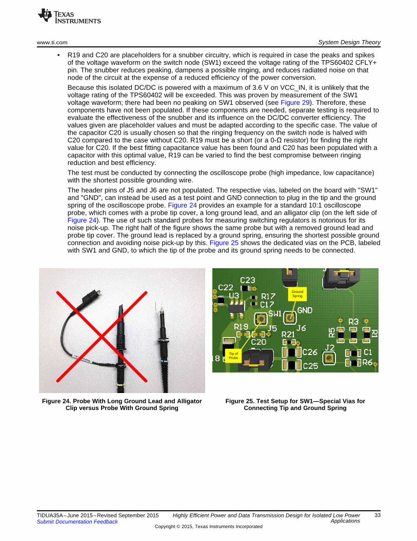
• R19 and C20 are placeholders for a snubber circuitry, which is required in case the peaks and spikesof the voltage waveform on the switch node (SW1) exceed the voltage rating of the TPS60402 CFLY+pin. The snubber reduces peaking, dampens a possible ringing, and reduces radiated noise on thatnode of the circuit at the expense of a reduced efficiency of the power conversion.Because this isolated DC/DC is powered with a maximum of 3.6 V on VCC_IN, it is unlikely that thevoltage rating of the TPS60402 will be exceeded. This was proven by measurement of the SW1voltage waveform; there had been no peaking on SW1 observed (see Figure 29). Therefore, thesecomponents have not been populated. If these components are needed, separate testing is required toevaluate the effectiveness of the snubber and its influence on the DC/DC converter efficiency. Thevalues given are placeholder values and must be adapted according to the specific case. The value ofthe capacitor C20 is usually chosen so that the ringing frequency on the switch node is halved withC20 compared to the case without C20. R19 must be a short (or a 0-Ω resistor) for finding the rightvalue for C20. If the best fitting capacitance value has been found and C20 has been populated with acapacitor with this optimal value, R19 can be varied to find the best compromise between ringingreduction and best efficiency.The test must be conducted by connecting the oscilloscope probe (high impedance, low capacitance)with the shortest possible grounding wire.The header pins of J5 and J6 are not populated. The respective vias, labeled on the board with "SW1"and "GND", can instead be used as a test point and GND connection to plug in the tip and the groundspring of the oscilloscope probe. Figure 24 provides an example for a standard 10:1 oscilloscopeprobe, which comes with a probe tip cover, a long ground lead, and an alligator clip (on the left side ofFigure 24). The use of such standard probes for measuring switching regulators is notorious for itsnoise pick-up. The right half of the figure shows the same probe but with a removed ground lead andprobe tip cover. The ground lead is replaced by a ground spring, ensuring the shortest possible groundconnection and avoiding noise pick-up by this. Figure 25 shows the dedicated vias on the PCB, labeledwith SW1 and GND, to which the tip of the probe and its ground spring needs to be connected.
Figure 24. Probe With Long Ground Lead and Alligator Figure 25. Test Setup for SW1—Special Vias forClip versus Probe With Ground Spring Connecting Tip and Ground Spring
33TIDUA35A–June 2015–Revised September 2015 Highly Efficient Power and Data Transmission Design for Isolated Low PowerApplicationsSubmit Documentation Feedback
Copyright © 2015, Texas Instruments Incorporated

System Design Theory www.ti.com
A comparison of the same switch-node signal measured with the standard probe configuration or withthe approach using the modified probe with the ground spring is shown in Figure 27 and Figure 29,respectively. The latter method provides a clean waveform compared to the standard probe usage,which shows peaking and ringing (highlighted by the red circles in Figure 27).The real measurementsetup is shown in Figure 26 and Figure 28, respectively.
Figure 26. Test Setup for SW1—Switch Node Voltage; Figure 27. SW1—Switch Node Voltage Waveform UsingUsing Probe With Long Ground Lead and Alligator Clip Probe With Long Ground Lead and Alligator Clip
Figure 28. Test Setup for SW1—Switch Node Voltage Figure 29. SW1—Switch Node Voltage Waveform UsingUsing Probe With Ground Spring Probe With Ground Spring
• R20 and R21 are used to keep the capacitive divider C25 and C26 balanced to cancel out theirpossible tolerances.
• L2 and L3 are ferrite beads used to filter high frequency noise (spikes with the switching frequency ofthe isolated DC/DC), which can be observed on C19+C24 but should be kept from C21.
34 Highly Efficient Power and Data Transmission Design for Isolated Low Power TIDUA35A–June 2015–Revised September 2015Applications Submit Documentation Feedback
Copyright © 2015, Texas Instruments Incorporated

GND1
VIN2
EN3
EN_HYS4
FB5
VOS6
SW7
PG8
PAD9
U4
TPS62125DSGR
10µFC30
10µFC29
10µFC28
10µFC27
GND_iso
GND_iso
GND_iso
L1
VLF302515MT-150M
PG_iso
2.00MR25
1.8MR22
576kR24
GND_iso
1.30MR23
499kR26
255kR27
GND_iso
IN1
7
OUT6
3
GND
U5A
TPS715A33DRVR NC2
NC4
NC5
U5B
TPS715A33DRVR
1µFC32
1
2
3
J191
2
3
J24SH-J19SH-J24
VCC_iso
GND_iso
1µFC31
1
J8
DNP
3.3V
3.3V
VOUT_isoDCDC
VIN_LDO
VIN_DCDC
VOUT_DCDC
VOUT_LDO
High Efficiency DC/DC
Switch Node 2SW 2
Low Iq LDO
www.ti.com System Design Theory
4.3.2 Post RegulatorsThe design offers the user the ability to select either a TPS715A33 as low Iq LDO (U5) or a high-efficiencyDC/DC converter based on a TPS62125 (U4) switching regulator as post regulator solution(see Figure 30). The LDO solution is by far the simplest solution for the implementation of the postregulator as long as the reduced efficiency compared to the switching regulator solution is acceptable.
The post regulators are powered off VOUT_isoDCDC, the non-regulated output of the isolated DC/DCconverter. Both post regulators are able to provide a stable and well regulated 3.3 V on their outputsVOUT_LDO or VOUT_DCDC. The design is characterized for output currents up to 10 mA.
space
Figure 30. Post Regulators—Real Implementation
The selection of the post regulators is done by simple jumper setting. Jumper J24 connects the output ofthe isolated DC/DC converter with the input VIN_LDO or VIN_DCDC of the selected post regulators. The 3.3-Voutput of the selected post regulator is connected through jumper J19 to VCC_iso on the isolated side. Thedetailed jumper settings applicable for the different power options and including the settings for J15 aredescribed in Section 5.2 and Table 11.
35TIDUA35A–June 2015–Revised September 2015 Highly Efficient Power and Data Transmission Design for Isolated Low PowerApplicationsSubmit Documentation Feedback
Copyright © 2015, Texas Instruments Incorporated

VIN_LDO VOUT_LDO
GND_iso
GND_iso
GND_iso
System Design Theory www.ti.com
4.3.2.1 Low Iq LDO—Circuit ImplementationThe TPS715A33 is shown as U5A and U5B in the schematic of Figure 30, where U5A is representing theLDO functionality and U5B is symbolizing the not connected pins of the device. The used LDO is a fixed3.3-V version, not needing any additional resistors to set up the output voltage. Tolerances andtemperature coefficients of external voltage setting resistors, as would be needed with the adjustableversion, do not need to be considered with the fixed 3.3-V device. The datasheet gives the output voltageaccuracy spec for the used 3.3-V version over the complete full input voltage (4.3 to 24 V), output current(0 to 80 mA) and operating junction temperature range (–40°C to 125°C). The circuit design follows theguidelines and recommendations of the datasheet.
External CapacitorsC31 and C32 are the bypass capacitors of the LDO’s input and output. 1-μF X5R capacitors have beenselected, fulfilling the datasheet recommendations of 0.47 μF with a reasonable margin. The voltage ratingfor the capacitors is 16 V for the input capacitor C31 and 10 V for the output capacitor C32 to reduce theeffects of DC bias (up to about 9 V for C31, 3.3 V for C32) on the capacitance values. Both capacitors areplaced as close as possible on the respective pins of the LDO as shown in Figure 31. The input andoutput of the LDO are forced to pass through the pads of the bypass caps. The GND pin of the LDO (pin 3of U5) is directly connected with C31 and C32 too. The LDO, the two bypass capacitors and theirinterconnections are placed on the same side of the PCB, not relying on vias for the electricalconnections. Vias are used only to connect the "GND-iso" net of the circuit and the PowerPAD of the LDOto the "GND_iso" plane inside the PCB.
Figure 31. Low Iq LDO—Board Layout and LDO’s Grounding
36 Highly Efficient Power and Data Transmission Design for Isolated Low Power TIDUA35A–June 2015–Revised September 2015Applications Submit Documentation Feedback
Copyright © 2015, Texas Instruments Incorporated

VIN
- Input Voltage - V
3 4 5 6 7 8 9 10 11 12 13 14 15
1400
1200
1000
800
600
400
200
0
VD
O-
Dro
po
ut
Vo
lta
ge
-m
V
TJ = +125ºC
TJ
= +25ºC
TJ
= –40ºC
DO _ max_125C _ 80mADO _ max_125C _10mA DO _ typ _ 25C _10mA
DO _ typ _ 25C _ 80mA
V 1120 mVV V 100 mV 167 mV
V 670 mV» ´ = ´ =
TJ
– Junction Temperature – ° C
-40 -25 -10 5 20 35 50 65 80 95 110 125
1000
900
800
700
600
500
400
300
200
100
0
VD
O–
Dro
pou
tV
oltag
e–
mV
VIN
= 4.3 V
IOUT
= 80 mA
IOUT
= 10 mA
www.ti.com System Design Theory
Dropout VoltageAs outlined in the TPS715A datasheet, the specification of the dropout voltage VDO is valid for thecondition when the pass-FET of the LDO is fully enhanced, so the LDO is performing under the VDO testcondition more as a (FET-) switch with a given RDS(ON) than a real voltage regulator. The VDO at an outputcurrent of 80 mA, which the LDO is rated for, is given in the datasheet with a typical value of 670 mV at25°C and a maximum value of 1.12 V at 125°C. The VDO can be scaled down for lower output currents asillustrated in Figure 32, giving also a typical value of roughly 100 mV at 125°C for an output current of10 mA.
Figure 32. TPS715A Dropout Voltage versus Junction
Applying the same ratio VDO_max_125C_80mA/VDO_typ_25C_80mA as given for the 80-mA output current to the 100 mVgiven as VDO_typ_25C_10mA will lead to an estimated maximum value for the dropout voltage at 10-mA outputcurrent and 125°C.
(10)
The 100 mV used as VDO_typ_25C_10mA in Equation 10 are valid for an input voltage of the LDO ≥ 4.3 V. Thevalue of the LDO’s VDO goes up with a lower input voltage as highlighted in Figure 33.
Figure 33. TPS715A Dropout Voltage versus Input Voltage
Nevertheless, as can be seen in the following section, the VDO is much smaller than VHR and does nottherefore need any further considerations in this design.
37TIDUA35A–June 2015–Revised September 2015 Highly Efficient Power and Data Transmission Design for Isolated Low PowerApplicationsSubmit Documentation Feedback
Copyright © 2015, Texas Instruments Incorporated

( ) ( )maxD _ 85C _10mA LDOP VIN_LDO _max VOUT _LDO _min IOUT 5.3 V 3.135 V 10 mA 22 mW+= - ´ = - ´ »
_ 40C _ 3mA HRVIN_LDO _min V VOUT _LDO _max 1 V 3.465 V 4.465 V 4.5 V-
= + = + = »
System Design Theory www.ti.com
Headroom VoltageBesides the dropout voltage, there is the so called headroom voltage VHR = VIN – VOUT, which needs tobe considered to get the full dynamical performance out of the LDO, namely the power supply ripplerejection (PSRR), as specified in the datasheet. In the case of the TPS715A, a 1-V headroom voltage wasused to perform PSRR measurements and to get the PSRR specifications as given in the electricalcharacteristics table and the PSRR versus Frequency graph of its datasheet. The needed VHR is related tothe output current, similarly as the VDO is. With the 10-mA output current specification of this design, theneeded VHR can be scaled down from its 1-V value given in the datasheet for the full 80-mA outputcurrent, but the down-scaling is not linear with IOUT as it can be done for the VDO. For this design, thedown-scaling was not applied.
Minimum Input VoltageBecause the main targeted applications of this design are loop-powered 4- to 20-mA transmitters, the goalis to ensure the best dynamic performance of the LDO for output currents of up to 3 mA. Therefore, theminimum needed input voltage of the LDO, VIN_LDO_min_-40C_3mA at the 3-mA level, and at –40°C were inthe range of 4.5 V as shown in Equation 11:
space
(11)
The voltage was defined at –40°C, because the output voltage of the isolated DC/DC (which is the inputvoltage of the LDO) is going down with lower temperatures. This is due to the negative temperaturecoefficient of the output diodes used in the isolated DC/DC. Furthermore, this voltage level needs to begenerated by the isolated DC/DC even at its lowest input voltage, VCC_IN_min of 3.0 V (see the blackVOUT curve in Figure 52).
Power DissipationThe LDO’s power dissipation PD needs to be calculated under worst case conditions, which areVIN_LDO_max_+85C_10mA, VOUT_LDO_min, and IOUT_LDO_max.
space
(12)
where• VIN_LDO_max_+85C_10mA is the maximum input voltage applied on the LDO at 85°C and at a 10-mA
output current. It equals the VOUT_isoDCDC at the respective temperature and current conditions andat an input voltage of the isolated DC/DC VCC_IN of 3.6 V
• VOUT_LDO_min is the minimum output voltage of the LDO as given in the TPS715A33 datasheetunder "Output Voltage Accuracy" in the "Electrical Characteristics" section of its datasheet
• IOUT_LDO_max is the maximum output current the LDO is providing in this design (10 mA)
The 22-mW power dissipation is much smaller than the dissipation ratings given in the respective sectionof the LDO’s datasheet.
38 Highly Efficient Power and Data Transmission Design for Isolated Low Power TIDUA35A–June 2015–Revised September 2015Applications Submit Documentation Feedback
Copyright © 2015, Texas Instruments Incorporated
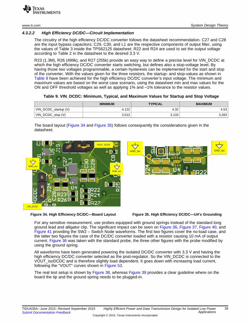
VIN_DCDC
VOUT_DCDC
GND_iso
GND_iso
GND_iso GND_iso
www.ti.com System Design Theory
4.3.2.2 High Efficiency DC/DC—Circuit ImplementationThe circuitry of the high efficiency DC/DC converter follows the datasheet recommendation. C27 and C28are the input bypass capacitors; C29, C30, and L1 are the respective components of output filter, usingthe values of Table 3 inside the TPS62125 datasheet. R22 and R24 are used to set the output voltageaccording to Table 2 in the datasheet to the desired 3.3 V.
R23 (1.3M), R26 (499k), and R27 (255k) provide an easy way to define a precise level for VIN_DCDC atwhich the high efficiency DC/DC converter starts switching, but defines also a stop-voltage level. Byhaving those two voltages programmable, a certain hysteresis can be implemented for the start and stopof the converter. With the values given for the three resistors, the startup- and stop-values as shown inTable 9 have been achieved for the high efficiency DC/DC converter’s input voltage. The minimum andmaximum values are based on the worst case scenario, using the datasheet min and max values for theON and OFF threshold voltages as well as applying 1% and –1% tolerance to the resistor values.
Table 9. VIN_DCDC: Minimum, Typical, and Maximum Values for Startup and Stop Voltage
MINIMUM TYPICAL MAXIMUMVIN_DCDC_startup (V) 4.122 4.32 4.53VIN_DCDC_stop (V) 3.012 3.133 3.283
The board layout (Figure 34 and Figure 35) follows consequently the considerations given in thedatasheet.
Figure 34. High Efficiency DC/DC—Board Layout Figure 35. High Efficiency DC/DC—U4’s Grounding
For any sensitive measurement, use probes equipped with ground springs instead of the standard longground lead and alligator clip. The significant impact can be seen on Figure 36, Figure 37, Figure 40, andFigure 41 providing the SW2 – Switch Node waveforms. The first two figures cover the no-load case, andthe latter two figures the case of the DC/DC converter loaded with a resistor causing 10 mA of outputcurrent. Figure 36 was taken with the standard probe, the three other figures with the probe modified byusing the ground spring.
All waveforms have been generated powering the isolated DC/DC converter with 3.3 V and having thehigh efficiency DC/DC converter selected as the post-regulator. So the VIN_DCDC is connected to theVOUT_isoDCDC and is therefore slightly load dependent. It goes down with increasing load current,following the "VOUT" curves shown in Figure 53.
The real test setup is shown by Figure 38, whereas Figure 39 provides a clear guideline where on theboard the tip and the ground spring needs to be plugged-in.
39TIDUA35A–June 2015–Revised September 2015 Highly Efficient Power and Data Transmission Design for Isolated Low PowerApplicationsSubmit Documentation Feedback
Copyright © 2015, Texas Instruments Incorporated
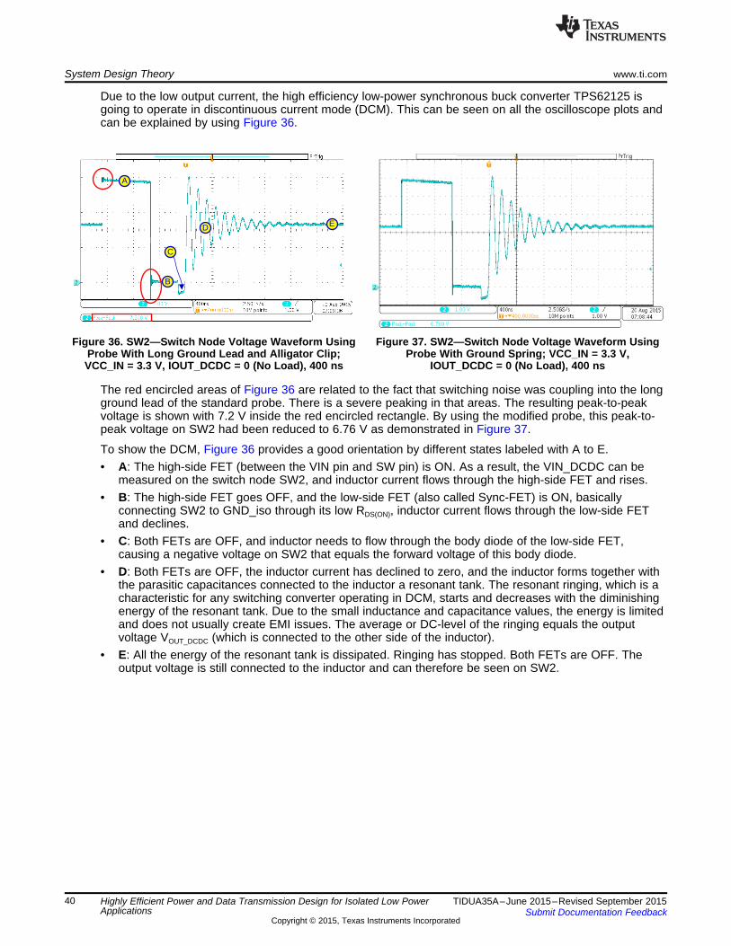
A
B
C
D E
System Design Theory www.ti.com
Due to the low output current, the high efficiency low-power synchronous buck converter TPS62125 isgoing to operate in discontinuous current mode (DCM). This can be seen on all the oscilloscope plots andcan be explained by using Figure 36.
Figure 36. SW2—Switch Node Voltage Waveform Using Figure 37. SW2—Switch Node Voltage Waveform UsingProbe With Long Ground Lead and Alligator Clip; Probe With Ground Spring; VCC_IN = 3.3 V,VCC_IN = 3.3 V, IOUT_DCDC = 0 (No Load), 400 ns IOUT_DCDC = 0 (No Load), 400 ns
The red encircled areas of Figure 36 are related to the fact that switching noise was coupling into the longground lead of the standard probe. There is a severe peaking in that areas. The resulting peak-to-peakvoltage is shown with 7.2 V inside the red encircled rectangle. By using the modified probe, this peak-to-peak voltage on SW2 had been reduced to 6.76 V as demonstrated in Figure 37.
To show the DCM, Figure 36 provides a good orientation by different states labeled with A to E.• A: The high-side FET (between the VIN pin and SW pin) is ON. As a result, the VIN_DCDC can be
measured on the switch node SW2, and inductor current flows through the high-side FET and rises.• B: The high-side FET goes OFF, and the low-side FET (also called Sync-FET) is ON, basically
connecting SW2 to GND_iso through its low RDS(ON), inductor current flows through the low-side FETand declines.
• C: Both FETs are OFF, and inductor needs to flow through the body diode of the low-side FET,causing a negative voltage on SW2 that equals the forward voltage of this body diode.
• D: Both FETs are OFF, the inductor current has declined to zero, and the inductor forms together withthe parasitic capacitances connected to the inductor a resonant tank. The resonant ringing, which is acharacteristic for any switching converter operating in DCM, starts and decreases with the diminishingenergy of the resonant tank. Due to the small inductance and capacitance values, the energy is limitedand does not usually create EMI issues. The average or DC-level of the ringing equals the outputvoltage VOUT_DCDC (which is connected to the other side of the inductor).
• E: All the energy of the resonant tank is dissipated. Ringing has stopped. Both FETs are OFF. Theoutput voltage is still connected to the inductor and can therefore be seen on SW2.
40 Highly Efficient Power and Data Transmission Design for Isolated Low Power TIDUA35A–June 2015–Revised September 2015Applications Submit Documentation Feedback
Copyright © 2015, Texas Instruments Incorporated

Tip of Probe
Ground Spring
www.ti.com System Design Theory
Figure 38. Test Setup for SW2—Switch Node Voltage Figure 39. Test Setup for SW2—Dedicated "Vias" forUsing Probe With Ground Spring Connecting Tip and Ground Spring
Figure 40. SW2—Switch Node Voltage Waveform Using Figure 41. SW2—Switch Node Voltage Waveform UsingProbe With Ground Spring; VCC_IN = 3.3 V, Probe With Ground Spring; VCC_IN = 3.3 V,
IOUT_DCDC = 10 mA, 4 μs IOUT_DCDC = 10 mA, 400 ns
Figure 40 and Figure 41 show the SW2 waveform for output currents of 10 mA. Figure 41 is similar toFigure 37; the time of state A is slightly prolonged and the voltage level during state A is reduced inFigure 41 due to the load dependency of the isolated DC/DC’s output voltage. Figure 40 covers the samecondition as Figure 41 but was taken with a larger time scale, allowing to see now the switching frequencyof the high efficiency DC/DC converter as well. Because the device is operating in DCM, the switchingfrequency is a function of the load current as well.
41TIDUA35A–June 2015–Revised September 2015 Highly Efficient Power and Data Transmission Design for Isolated Low PowerApplicationsSubmit Documentation Feedback
Copyright © 2015, Texas Instruments Incorporated

JTAG ConnectorJTAG Connector
BoosterPackConnectors
BoosterPackConnectors
Isolated Board SideNon-Isolated Board Side
J16
J15
J11J18
J23
J22
J19J7
Isolation
J24
J4
J17
J1
Getting Started Hardware www.ti.com
5 Getting Started Hardware
5.1 Headers and Jumper LocationsFigure 42 shows the jumpers found on TIDA-00459.
Figure 42. TIDA-00459 Jumper Locations
Table 10 shows the different functions of the headers.
Table 10. Jumper Functions
HEADERS DESCRIPTIONJ1 and J4 can be used to disconnect the two MSP430FR5969 from the isolation circuitry and the transformer onJ1, J4 the board. Instead, the jumpers can be used to connect different isolation circuits and transformers.
J7 J7 can be used to measure the current into the isolated side.J11 Isolated VCC and GND connection.
If the MSP430 on the isolated side is not powered from the MSP-FET Debugger, make sure pin 2 and pin 3 areJ15 connected on header J15. If power from the MSP-FET Debugger must be used, make sure pin 1 and pin 2 are
connected on header J15.J16 can be used to measure the current on the isolated side if the isolated side is powered from external VCC orJ16 MSP-FET Debugger.
J17 J17 can be used to measure the current on the primary side of the power transformer.J18 Non-isolated VCC and GND connection.
The LDO is selected for the isolated VCC if pin 1 and pin 2 are connected on J19. The DC/DC is selected for theJ19 isolated VCC if pin 2 and pin 3 are connected on J19.If the MSP430 on the non-isolated side is not powered from the MSP-FET Debugger, make sure pin 2 and pin 3
J22 are connected on jumper J22. If power from the MSP-FET Debugger must be used, make sure pin 1 and pin 2 areconnected on header J22.
J23 J23 can be used to measure the overall current of the board.The DC/DC is powered if pin 1 and pin 2 are connected on J24. The LDO is powered if pin 2 and pin 3 areJ24 connected on J24.
42 Highly Efficient Power and Data Transmission Design for Isolated Low Power TIDUA35A–June 2015–Revised September 2015Applications Submit Documentation Feedback
Copyright © 2015, Texas Instruments Incorporated
www.ti.com Getting Started Hardware
5.2 Power OptionsOn the TIDA-00459 are different power options for the non-isolated side and the isolated side. The non-isolated side can be powered from the external VCC on header J18 or from the JTAG MSP-FETDebugger.
The isolated side can be powered from the LDO, from the high efficiency DC/DC, from the external VCCon header J11, or from the MSP-FET Debugger.
If an external power supply is used during debug, make sure pin 2 and pin 3 are connected on header J22for the non-isolated side and respectively on header J15 for the isolated side. If there is no external powerconnected and power from the MSP-FET Debugger Interface should be used, make sure pin 1 and pin 2are connected on header J22 and respectively on header J15. The different jumper settings for the poweroptions on the isolated side can be found in Table 11.
Table 11. Power Options on Isolated Side
JUMPER PLACEMENT ON HEADERSPOWER OPTIONS ON ISOLATED SIDE
J15 J19 J24Power from LDO 2→3 1→2 1→2Power from high efficiency DC/DC 2→3 2→3 2→3Power from external VCC on J11 2→3 — —Power from MSP-FET Debugger on J9 1→2 — —
43TIDUA35A–June 2015–Revised September 2015 Highly Efficient Power and Data Transmission Design for Isolated Low PowerApplicationsSubmit Documentation Feedback
Copyright © 2015, Texas Instruments Incorporated
Getting Started Firmware www.ti.com
6 Getting Started FirmwareTo download the software files for this reference design, please see the link athttp://www.ti.com/tool/TIDA-00459.
6.1 Software Setup
1. Install Code Composer Studio™ (CCS) before connecting the MSP-FET to PC. While CCS installs,USB drivers are installed automatically. Make sure to use the latest CCS version; otherwise, the USBdrivers might not be able to recognize the MSP-FET.
2. Connect the MSP-FET to a USB port on the PC with the provided USB cable.3. The following procedure applies when using Windows®:
(a) After connecting to the PC, the MSP-FET should be recognized automatically, as the USB devicedriver has been already installed together with the IDE.
(b) If the driver has not been installed yet, the Found New Hardware wizard starts. Follow theinstructions and point the wizard to the driver files.
(c) The default location for CCS is c:\ti\ccsv6\ccs_base\emulation\drivers\msp430\USB_CDC.4. After connecting to a PC, the MSP-FET performs a self-test. If the self-test passes successfully, the
green LED stays on.5. If an external power supply is used during debug, make sure pin 2 and pin 3 are connected on jumper
J15 and respectively on jumper J22. If there is no external power connected and power from theMSP-FET Debugger Interface should be used, make sure pin 1 and pin 2 are connected on jumperJ15 and respectively on jumper J22.
6. Connect the MSP-FET with the 14-conductor cable to the JTAG connector J10 on the non-isolatedside of the TIDA-00459 board.
7. Import the CCS project (TIDA-00459) into CCS.8. Make sure following line has been commented out in the file main.h:
// #define MSP430_IS_ON_ISOLATED_SIDE9. Compile and download the firmware to the MSP430FR5969 on the non-isolated side of the
TIDA-00459 board.10. Connect the MSP-FET with the 14-conductor cable to the JTAG connector J9 on the isolated side of
the TIDA-00459 board.11. Make sure following line has been uncommented in the file main.h:
#define MSP430_IS_ON_ISOLATED_SIDE12. Compile and download the firmware to the MSP430FR5969 on the isolated side of the TIDA-00459
board.13. To start the data transmission from the non-isolated side, hit the button S4. To start the data
transmission from the isolated side, hit the button S1.
44 Highly Efficient Power and Data Transmission Design for Isolated Low Power TIDUA35A–June 2015–Revised September 2015Applications Submit Documentation Feedback
Copyright © 2015, Texas Instruments Incorporated

www.ti.com Getting Started Firmware
6.2 Software Function DocumentationThe file swif.c contains the functions for the data transmission:• void initCompE(void)
This function is called to configure the Comparator_E• void config_USCIA0_UART(uint16_t div)
This function is called to configure the eUSCIA0 module in UART mode.• void sendByte(uint8_t x)
This function is called to send the break/synch field plus one byte. The parameter x is the byte to send.• void sendByte_RX(uint8_t x)
This function is called to send the break/synch field plus one byte. After transmission is completed, theMSP430 is configured for receive again. The parameter x is the byte to send.
• void prepareTX(void)This function is called to prepare the MSP430 for TX mode.
• void prepareRX(void)This function is called to prepare the MSP430 for RX mode.
6.3 Demo Software: Bidirectional CommunicationThe software files can be downloaded at http://www.ti.com/tool/TIDA-00459. The CCS projectTIDA-00459_bidirectional is an example project for bidirectional communication.
The transmission starts on the non-isolated side with the button S4 or on the isolated side with the buttonS1. The value for the first transmitted byte is 0x00. When the byte has been received on the other side ofthe isolation, it is echoed back. The value is then incremented by one and sent again. If the value of theechoed back byte is not the same as the transmitted byte, the red LED lights up to show an error. Aftertransmitting 1k bytes, the green LED toggles. The transmission can be stopped with button S1 or S4. TheLEDs can be disabled with the buttons S2 and S3 or S5 and S6 to measure the current consumption ofthe data transmission.
45TIDUA35A–June 2015–Revised September 2015 Highly Efficient Power and Data Transmission Design for Isolated Low PowerApplicationsSubmit Documentation Feedback
Copyright © 2015, Texas Instruments Incorporated

Test Setup and Test Data www.ti.com
7 Test Setup and Test DataSeveral tests have been conducted. The complete isolated power path as well as the isolated datatransmission have been first tested separately from each other, followed by the test of the complete board.
7.1 Power PathThe test of the complete power path includes the performance evaluation of all power blocks of this designat ambient temperatures of –40°C, 25°C, and 85°C:• Isolated DC/DC• Post regulators
– Low Iq LDO– High efficiency DC/DC
The test was conducted by measuring and recording the input voltage and current on the input header J7of the open loop isolated DC/DC. SMU 1 was used as programmable power supply, the output voltage ofSMU1 was stepped from 3 to 3.6 V in 300-mV steps to evaluate the performance over the full inputvoltage range as specified in Section 1.
The regulated 3.3-V output voltage and current of the two different post regulators were measured andrecorded on the respective pins of header J19 (see Table 13). This output currents can be considered asthe load current of the post regulators. A second SMU (SMU 2) was set up to sweep this load current from1 μA up to 10 mA. By using such a wide output current range for this test, the performance of the powerpath can be evaluated for the different load situation commonly seen in applicable applications, rangingfrom low power modes (Shutdown, Standby) up to maximum load situation (active mode at different clockspeed + additional application specific current consumption). In addition the voltage and currents on theinterface header J24, connecting the output of the isolated DC/DC with the input of the post regulators,have been recorded. The current measurement was done by DMM 1, a high-resolution voltmeter using anexternal 1-Ω precision resistor as a current sense shunt. This approach was preferred versus the normalway of configuring the DMM as an ammeter. The latter ammeter configuration would have been causinghigher voltage drops based on the larger internal precision shunt (often 5 Ω) and the protection fuses(often two fuses: one inside the DMM, the other one a replaceable fuse located on the DMM’s rear panel).These protection fuses are connected in series to the internal precision shunt but their resistance is notspecified at all.
By having all the voltages and currents on the input (J7), on the output (J19), and on the interface header(J24), the performance of the total power path (isolated DC/DC + post regulator) as well of the separatepower blocks can be evaluated and characterized.
46 Highly Efficient Power and Data Transmission Design for Isolated Low Power TIDUA35A–June 2015–Revised September 2015Applications Submit Documentation Feedback
Copyright © 2015, Texas Instruments Incorporated
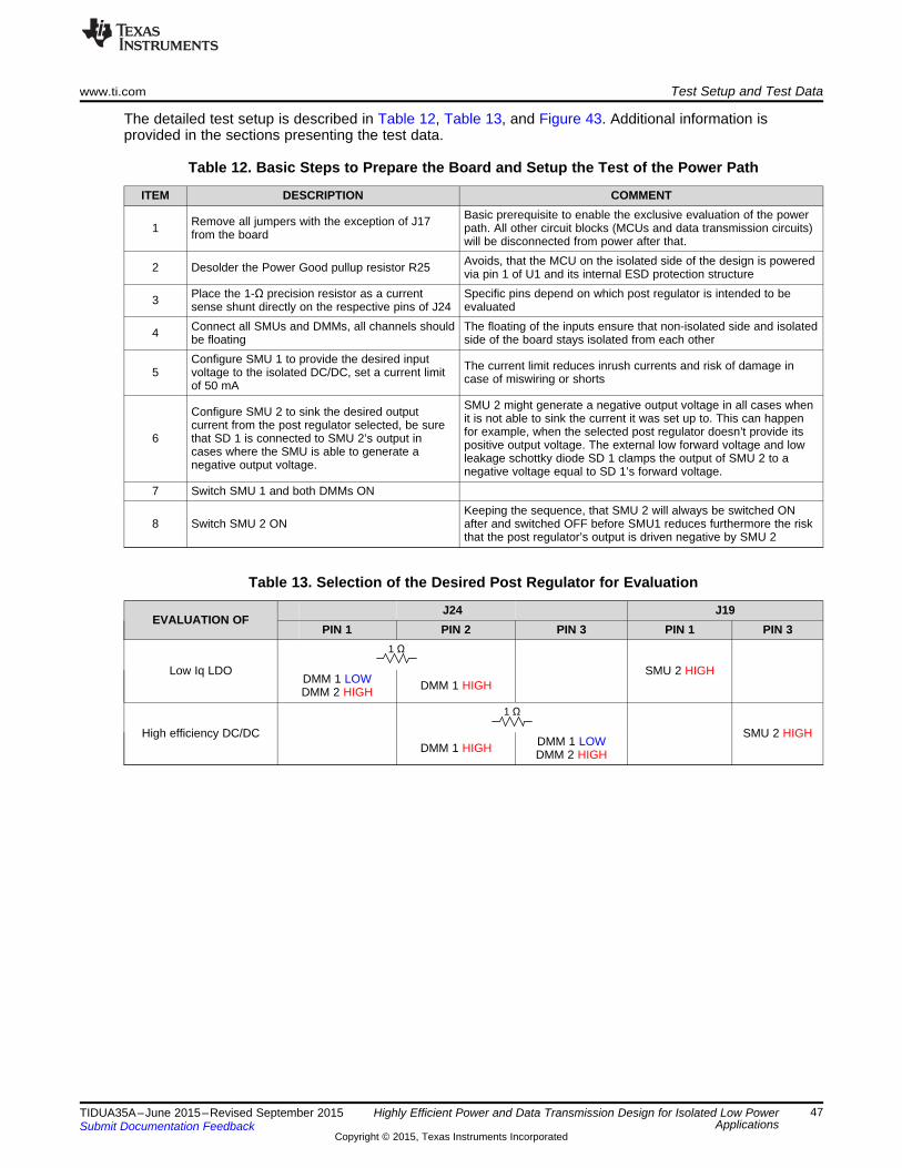
1
1
www.ti.com Test Setup and Test Data
The detailed test setup is described in Table 12, Table 13, and Figure 43. Additional information isprovided in the sections presenting the test data.
Table 12. Basic Steps to Prepare the Board and Setup the Test of the Power Path
ITEM DESCRIPTION COMMENTBasic prerequisite to enable the exclusive evaluation of the powerRemove all jumpers with the exception of J171 path. All other circuit blocks (MCUs and data transmission circuits)from the board will be disconnected from power after that.Avoids, that the MCU on the isolated side of the design is powered2 Desolder the Power Good pullup resistor R25 via pin 1 of U1 and its internal ESD protection structure
Place the 1-Ω precision resistor as a current Specific pins depend on which post regulator is intended to be3 sense shunt directly on the respective pins of J24 evaluatedConnect all SMUs and DMMs, all channels should The floating of the inputs ensure that non-isolated side and isolated4 be floating side of the board stays isolated from each otherConfigure SMU 1 to provide the desired input The current limit reduces inrush currents and risk of damage in5 voltage to the isolated DC/DC, set a current limit case of miswiring or shortsof 50 mA
SMU 2 might generate a negative output voltage in all cases whenConfigure SMU 2 to sink the desired output it is not able to sink the current it was set up to. This can happencurrent from the post regulator selected, be sure for example, when the selected post regulator doesn’t provide its6 that SD 1 is connected to SMU 2’s output in positive output voltage. The external low forward voltage and lowcases where the SMU is able to generate a leakage schottky diode SD 1 clamps the output of SMU 2 to anegative output voltage. negative voltage equal to SD 1’s forward voltage.7 Switch SMU 1 and both DMMs ON
Keeping the sequence, that SMU 2 will always be switched ON8 Switch SMU 2 ON after and switched OFF before SMU1 reduces furthermore the risk
that the post regulator’s output is driven negative by SMU 2
Table 13. Selection of the Desired Post Regulator for Evaluation
J24 J19EVALUATION OF
PIN 1 PIN 2 PIN 3 PIN 1 PIN 3
Low Iq LDO SMU 2 HIGHDMM 1 LOW DMM 1 HIGHDMM 2 HIGH
High efficiency DC/DC SMU 2 HIGHDMM 1 LOWDMM 1 HIGH DMM 2 HIGH
47TIDUA35A–June 2015–Revised September 2015 Highly Efficient Power and Data Transmission Design for Isolated Low PowerApplicationsSubmit Documentation Feedback
Copyright © 2015, Texas Instruments Incorporated

Post Regulators
Half-BridgeDriver
TPS60402
VoltageDoubler
2 x
Isol
atio
n
Isolated SideNon-Isolated Side
Low Iq LDO
TPS715A33
High Efficiency DC/DC
TPS62125
MCU
MSP430FR5969
MCU
MSP430FR5969
GND
GND GND_iso
J11
J15
J16
J19
J24
J17
J7
J23
J22
GND
Power Transformer
VCC
3 to 3.6 V
VCC / 2
J1 J4
VCC_iso
GND_iso
J18
3.3V
3.3V
Isolated DC/DC
R25 2M
PG_iso
1 21 2 3
12
3
SMU 1 used as Programmable Power Supply(VCCIN and J7 ± IIN)
HIGH
LOW
SENSE FORCEV A
HIGH
LOW
SENSE FORCEV A
HIGH LOW
IN
VHIGH LOW
IN
V
SMU 2 used as Programmable Load Current Sink (VOUT and J19 ± IOUT of Regulated 3.3-V Rail)
DMM 1 (8 ½ Digit)(J24 ± IOUT of Isolated DC/DC)
DMM 2 (6 ½ Digit)(J24 ± VIN of Post Regulators and
VOUT of Isolated DC/DC)
1
External
Precision
Shunt *
J24 ± pin 1** o
r
J24 ± pin 3**
J19 ± pin 1** orJ19 ± pin 3**
* place as close as possible on J24
** depending on which post regulator is intended for evaluation
*** desolder for power path performance evaluation
1 2
3 1 2
3
SD1External Schottky Diode
(Low VF, low IR)
Protection of Post Regulators Outputs Against Negative Voltage of SMU2 in Case RI�0LVVLQJ�3RVW�5HJXODWRUV¶�2XWSXW�9ROWDJH�
***
t
tt
t
Test Setup and Test Data www.ti.com
Figure 43. Test Setup for Evaluation of the Power Path
48 Highly Efficient Power and Data Transmission Design for Isolated Low Power TIDUA35A–June 2015–Revised September 2015Applications Submit Documentation Feedback
Copyright © 2015, Texas Instruments Incorporated

J19 - IOUT (mA)
To
talE
ffic
ien
cy (
%)
0.001 0.01 0.1 1 100
10
20
30
40
50
60
70
80
D003
with Low Iq LDOas Post Regulator
with High EfficiencyDC/DC as Post Regulator
T = +85°C
VCCIN = 3.0 VVCCIN = 3.3 VVCCIN = 3.6 V
A
J19 - IOUT (mA)
To
talE
ffic
ien
cy (
%)
0.001 0.01 0.1 1 100
10
20
30
40
50
60
70
80
D016
with Low Iq LDOas Post Regulator
with High EfficiencyDC/DC as Post Regulator
VCCIN = 3.3 V
T = -40°CT = +25°CT = +85°CA
A
A
J19 - IOUT (mA)
To
talE
ffic
ien
cy (
%)
0.001 0.01 0.1 1 100
10
20
30
40
50
60
70
80
D001
with Low Iq LDOas Post Regulator
with High EfficiencyDC/DC as Post Regulator
T = -40°C
VCCIN = 3.0 VVCCIN = 3.3 VVCCIN = 3.6 V
A
J19 - IOUT (mA)
To
talE
ffic
ien
cy (
%)
0.001 0.01 0.1 1 100
10
20
30
40
50
60
70
80
D002
with Low Iq LDOas Post Regulator
with High EfficiencyDC/DC as Post Regulator
T = +25°C
VCCIN = 3.0 VVCCIN = 3.3 VVCCIN = 3.6 V
A
www.ti.com Test Setup and Test Data
7.1.1 Efficiency of Complete Power PathFigure 44 to Figure 47 present the total efficiency numbers of the complete power path ranging from theinput of the isolated DC/DC (J7) to the output of the selected post regulator (J19). Each of the chartsshows the curves taken with the high efficiency DC/DC as well as with the low Iq LDO as post regulatorfor easy comparison. The post regulators are set up to provide an output voltage of 3.3 V.
In Figure 44 to Figure 46, the three curves provided for each version of the selected post regulatorrepresent the performance at the three different input voltages VCCIN (3, 3.3, and 3.6 V) of the isolatedDC/DC. The version using the high efficiency DC/DC provides a better efficiency, especially for outputcurrents larger than 100 μA. The efficiency improvement is up to 30% for output currents exceeding a2-mA level. Figure 47 highlights the temperature dependency of the efficiency at the nominal input voltageof 3.3 V.
Figure 44. Total Efficiency at TA = –40°C Figure 45. Total Efficiency at TA = 25°C
Figure 46. Total Efficiency at TA = 85°C Figure 47. Total Efficiency at VCCIN = 3.3 V
49TIDUA35A–June 2015–Revised September 2015 Highly Efficient Power and Data Transmission Design for Isolated Low PowerApplicationsSubmit Documentation Feedback
Copyright © 2015, Texas Instruments Incorporated

J19 - IOUT (mA)
J7
- I I
N(m
A)
0.001 0.01 0.1 1 100.1
1
10
2020
D015
with Low Iq LDOas Post Regulator
with HighEfficiencyDC/DC asPost Regulator
T = +85°C
VCCIN = 3.0 VVCCIN = 3.3 VVCCIN = 3.6 V
A
J19 - IOUT (mA)
J7
- I I
N(m
A)
0.001 0.01 0.1 1 100.1
1
10
2020
D020
VCCIN = 3.3 V
with Low Iq LDOas Post Regulator
with HighEfficiencyDC/DC asPost Regulator
T = -40°CT = +25°CT = +85°C
A
A
A
J19 - IOUT (mA)
J7
- I I
N(m
A)
0.001 0.01 0.1 1 100.1
1
10
2020
D013
with Low Iq LDOas Post Regulator
with HighEfficiencyDC/DC asPost Regulator
T = -40°C
VCCIN = 3.0 VVCCIN = 3.3 VVCCIN = 3.6 V
A
J19 - IOUT (mA)
J7
- I I
N(m
A)
0.001 0.01 0.1 1 100.1
1
10
2020
D014
with Low Iq LDOas Post Regulator
with HighEfficiencyDC/DC asPost Regulator
T = +25°C
VCCIN = 3.0 VVCCIN = 3.3 VVCCIN = 3.6 V
A
Test Setup and Test Data www.ti.com
7.1.2 Input Current Consumption of the Complete Power PathFigure 48 to Figure 50 present the total input current J7 – IIN, which is drawn by the complete power path.
The graphs provide a straight-forward way to cross check whether the current consumption will stay belowa certain value for a given output current. This is especially helpful in applications with a limited currentbudget, such as loop-powered 4- to 20-mA sensor transmitters, metering applications, or systems usingenergy harvesting. The input current is measured by SMU 1, which feeds the isolated DC/DC converterwith an input voltage VCCIN of 3, 3.3, and 3.6 V. J19-IOUT is the output current of the selected postregulator, which is controlled by SMU 2 operating as current sink.
The plotted curves using solid lines to present the total input current when using the high efficiency DC/DCas post regulator. The case of using the low Iq LDO as post regulator is represented by the curves usingdifferent dashed and dotted lines. Figure 51 highlights the temperature dependency of the input currentconsumption of the complete power path at the nominal input voltage of 3.3 V.
Figure 48. Total Input Current at TA = –40°C Figure 49. Total Input Current at TA = 25°C
Figure 50. Total Input Current at TA = 85°C Figure 51. Total Input Current at VCCIN = 3.3 V
50 Highly Efficient Power and Data Transmission Design for Isolated Low Power TIDUA35A–June 2015–Revised September 2015Applications Submit Documentation Feedback
Copyright © 2015, Texas Instruments Incorporated

J24 - IOUT (mA)
Effic
ien
cy
of
Iso
late
d D
C/D
C(%
)
J2
4 -
VO
UT
(V)
0.001 0.01 0.1 1 100 1.0
10 2.0
20 3.0
30 4.0
40 5.0
50 6.0
60 7.0
70 8.0
80 9.0
90 10.0
D004
Vout
Efficiency
T = -40°C
VCCIN = 3.0 VVCCIN = 3.3 VVCCIN = 3.6 V
A
J24 - IOUT (mA)
Effic
ien
cy
of
Iso
late
d D
C/D
C(%
)
J2
4 -
VO
UT
(V)
0.001 0.01 0.1 1 100 1.0
10 2.0
20 3.0
30 4.0
40 5.0
50 6.0
60 7.0
70 8.0
80 9.0
90 10.0
D005
Vout
Efficiency
T = +25°C
VCCIN = 3.0 VVCCIN = 3.3 VVCCIN = 3.6 V
A
www.ti.com Test Setup and Test Data
7.1.3 Efficiency and Output Voltage of Isolated DC/DCFigure 52 to Figure 55 present the curves for the efficiency and for the output voltage of the isolatedDC/DC, based on the measurements of SMU 1, DMM 1, and DMM 2. The SMU 1 sets the input voltage(VCCIN of 3, 3.3, and 3.6 V) and measures the input current J7 – IIN to get the total input power.
To load the isolated DC/DC, the complete power path was used as described in Section 7.1.1 andSection 7.1.2. The low Iq LDO was selected as post regulator by adequate J24 and J19 setup andconfiguration according to Table 13. SMU 2 was used to sink a current from the post regulator’s outputfrom 1 μA up to 10 mA. SMU 2 was used in this case for controlling the sinking current only. The voltageand current values measured by SMU 2 have not been used in this case, because they do not representthe output voltage and output current of the isolated DC/DC but the values on the output of the postregulator.
The output current of the isolated DC/DC is derived instead by the voltage drop measured with DMM1across the external 1-Ω precision shunt resistor. The output voltage of the isolated DC/DC (J24-VOUT) ismeasured with DMM 2 on the input of the low Iq LDO. This voltage differs at 10-mA current flow throughthe 1-Ω shunt only by 10 mV from the real voltage at the output of the isolated DC/DC. This small 10-mVerror is neglectable at the respective output voltage level of at least 4 V.
The derived output voltage and current of the isolated DC/DC was used to calculate its output power andfinally to calculate its efficiency by factoring in the before calculated input power. Beside the efficiency, theoutput voltage (J24-VOUT) is plotted into the same graphs to show the output voltage’s load, inputvoltage, and temperature dependency. The light or no load output voltage is especially important to knowwhen it comes to the selection of a linear or switching post regulator. The post regulator needs to be ableto withstand the high output voltage of the isolated DC/DC under such load conditions. Factor in anadditional adequate margin.
Figure 55 highlights the temperature dependency of the isolated DC/DC’s efficiency and output voltage atthe nominal input voltage of 3.3 V.
Figure 52. Efficiency and Output Voltage of Isolated Figure 53. Efficiency and Output Voltage of IsolatedDC/DC at TA = –40°C DC/DC at TA = 25°C
51TIDUA35A–June 2015–Revised September 2015 Highly Efficient Power and Data Transmission Design for Isolated Low PowerApplicationsSubmit Documentation Feedback
Copyright © 2015, Texas Instruments Incorporated

J24 - IOUT (mA)
Effic
ien
cy
of
Iso
late
d D
C/D
C(%
)
J2
4 -
VO
UT
(V)
0.001 0.01 0.1 1 100 1.0
10 2.0
20 3.0
30 4.0
40 5.0
50 6.0
60 7.0
70 8.0
80 9.0
90 10.0
D006
Vout
Efficiency
T = +85°C
VCCIN = 3.0 VVCCIN = 3.3 VVCCIN = 3.6 V
A
J24 - IOUT (mA)
Effic
ien
cy
of
Iso
late
d D
C/D
C(%
)
J2
4 -
VO
UT
(V)
0.001 0.01 0.1 1 100 1.0
10 2.0
20 3.0
30 4.0
40 5.0
50 6.0
60 7.0
70 8.0
80 9.0
90 10.0
D017
VCCIN = 3.3 V
Vout
Efficiency
T = -40°CT = +25°CT = +85°CA
A
A
Test Setup and Test Data www.ti.com
Figure 54. Efficiency and Output Voltage of Isolated Figure 55. Efficiency and Output Voltage of IsolatedDC/DC at TA = 85°C DC/DC at VCCIN = 3.3 V
7.1.4 Efficiency and Output Voltage of High Efficiency DC/DCFigure 56 to Figure 59 present the curves for the efficiency and for the output voltage of the high efficiencyDC/DC, based on the measurements of SMU 1, DMM 1, DMM 2, and SMU 2. The high efficiency DC/DCwas selected as post regulator by adequate J24 and J19 setup and configuration according to Table 13.
The SMU 1 sets the input voltage (VCCIN of 3, 3.3, and 3.6 V) of the isolated DC/DC applied to pin 2 ofJ7. SMU 2 was used to sink a current from 1 μA up to 10 mA as load current from the output of the highefficiency DC/DC. This load current (J19-IOUT) was used together with the output voltage (J19-VOUT)measured by SMU 2 to calculate the output power of the high efficiency DC/DC.
The input power of the high efficiency DC/DC have been derived by using the voltage drop measured withDMM1 across the external 1-Ω precision shunt resistor as input current. The input voltage of the highefficiency DC/DC was measured with DMM 2 on the pin 3 of J24.
The measured values of SMU 1 of the input voltage and input current on J7 have not been used in thiscase to create the efficiency curves directly because they do not represent the input power of the highefficiency DC/DC but the input power of the isolated DC/DC. Nevertheless, the three different values thatSMU 1 was set up to provide as VCCIN have been finally used to create for each chart three differentefficiency and VOUT curves. Those three different curves can be used to characterize the input voltagedependency of the high efficiency DC/DC. VCCIN is the input voltage applied to the isolated DC/DC but notthe real input voltage of the high efficiency DC/DC. The input voltage of the high efficiency DC/DCbasically equals the output voltage of the isolated DC/DC, so it changes with loading of the isolatedDC/DC as shown in Figure 52 to Figure 55. This restriction is based on the fact that all the performanceevaluation and data collection had been done for the complete power path but not for the single powerblocks separately. The real input voltage of the high efficiency DC/DC can be approximated by using thedifferent test data graphs using the following steps:1. Know the following parameters and conditions: ambient temperature T, input voltage VCCIN applied to
J7-pin 2, output load current J19-IOUT.Example: T = 25°C, VCCIN = 3.3 V, J19-IOUT = 100 μA
2. Determine the efficiency ηHigh Efficiency DC/DC of the high efficiency DC/DC at the given conditions using therespective graphs provided in Section 7.1.4.Example: using Figure 57; ηHigh Efficiency DC/DC ≈ 68%
3. Determine the total efficiency ηTotal of the complete power path at the given conditions using the "withHigh Efficiency DC/DC as Post Regulator" curves of the respective graphs provided in Section 7.1.1.Example: using Figure 45; ηTotal ≈ 39.5%
52 Highly Efficient Power and Data Transmission Design for Isolated Low Power TIDUA35A–June 2015–Revised September 2015Applications Submit Documentation Feedback
Copyright © 2015, Texas Instruments Incorporated

J19 - IOUT (mA)
Effic
ien
cy o
fH
igh
Eff
icie
ncy D
C/D
C(%
)
J1
9-
VO
UT
(V)
0.001 0.01 0.1 1 100 3.310
10 3.312
20 3.314
30 3.316
40 3.318
50 3.320
60 3.322
70 3.324
80 3.326
90 3.328
100 3.330
D009
Vout
Efficiency
T = +85°C
VCCIN = 3.0 VVCCIN = 3.3 VVCCIN = 3.6 V
A
J19 - IOUT (mA)
Effic
ien
cy o
fH
igh
Eff
icie
ncy D
C/D
C(%
)
J1
9-
VO
UT
(V)
0.001 0.01 0.1 1 100 3.308
10 3.312
20 3.316
30 3.320
40 3.324
50 3.328
60 3.332
70 3.336
80 3.340
90 3.344
100 3.348
D018
VCCIN = 3.3 V
Vout
Efficiency
T = -40°CT = +25°CT = +85°CA
A
A
J19 - IOUT (mA)
Effic
ien
cy o
fH
igh
Eff
icie
ncy D
C/D
C(%
)
J1
9-
VO
UT
(V)
0.001 0.01 0.1 1 100 3.320
10 3.322
20 3.324
30 3.326
40 3.328
50 3.330
60 3.332
70 3.334
80 3.336
90 3.338
100 3.340
D007
Vout
Efficiency
T = -40°C
VCCIN = 3.0 VVCCIN = 3.3 VVCCIN = 3.6 V
A
J19 - IOUT (mA)
Effic
ien
cy o
fH
igh
Eff
icie
ncy D
C/D
C(%
)
J1
9-
VO
UT
(V)
0.001 0.01 0.1 1 100 3.310
10 3.312
20 3.314
30 3.316
40 3.318
50 3.320
60 3.322
70 3.324
80 3.326
90 3.328
100 3.330
D008
Vout
Efficiency
T = +25°C
VCCIN = 3.0 VVCCIN = 3.3 VVCCIN = 3.6 V
A
TotalIsolatedDC/DC
High Efficiency DC/DC
0.3950.58
0.68
hh = » »
h
TotalIsolated DC/DC
High Efficiency DC/DC
hh =
h
www.ti.com Test Setup and Test Data
4. Calculate the efficiency ηIsolated DC/DC of the isolated DC/DC using
(13)
5. Use the graphs provided in Section 7.1.3 to determine an approximated value for the input voltage ofthe high efficiency DC/DC (J24-VIN), which is equal to the J24-VOUT value shown on the right verticalaxis of the graphs. If the graphs and curves for the applicable ambient temperature T and input voltageVCCIN are used, the J24-VIN can be found on the VOUT curves at the J24-IOUT value resulting in theefficiency ηIsolated DC/DC of the isolated DC/DC as calculated in the previous step. See the followingexample:• Using the efficiency curves of Figure 53 to find J24-IOUT at which ηIsolated DC/DC ≈ 0.58
J24-IOUT = 90 μA• Using VOUT curves of Figure 53 to determine the VOUT at the previously found J24-IOUT:
VOUT ≈ 5.55 V at J24-IOUT = 90 μA
Figure 56. Efficiency and Output Voltage of High Figure 57. Efficiency and Output Voltage of HighEfficiency DC/DC at TA = –40°C Efficiency DC/DC at TA = 25°C
Figure 58. Efficiency and Output Voltage of High Figure 59. Efficiency and Output Voltage of HighEfficiency DC/DC at TA = 85°C Efficiency DC/DC at VCCIN = 3.3 V
53TIDUA35A–June 2015–Revised September 2015 Highly Efficient Power and Data Transmission Design for Isolated Low PowerApplicationsSubmit Documentation Feedback
Copyright © 2015, Texas Instruments Incorporated

J24 _IOUT 10 A 3.2 A 13.2 A
J24 VIN at 13.2 µA 6.25 V- »
» m + m = m
U5J24 _IOUT J19 _IOUT Iq J19 _IOUT 3.2 A= + » + m
Test Setup and Test Data www.ti.com
7.1.5 Efficiency and Output Voltage of Low Iq LDOFigure 60 to Figure 63 present the curves for the efficiency and for the output voltage of the low Iq LDO,based on the measurements of SMU 1, DMM 1, DMM 2, and SMU 2. The low Iq LDO was selected aspost regulator by adequate J24 and J19 setup and configuration according to Table 13.
The SMU 1 sets the input voltage (VCCIN of 3, 3.3, and 3.6 V) of the isolated DC/DC applied to pin 2 ofJ7. SMU 2 was used to sink a current from 1 μA up to 10 mA as a load current from the low Iq LDO. Thisload current (J19-IOUT) was used together with the output voltage (J19-VOUT) measured by SMU 2 tocalculate the output power of the low Iq LDO.
The input power of the low Iq LDO have been derived by using the voltage drop measured with DMM1across the external 1-Ω precision shunt resistor as input current. The input voltage of the low Iq LDO wasmeasured with DMM 2 on the pin 1 of J24.
The measured values of SMU 1 of the input voltage and input current on J7 have not been used in thiscase to create the efficiency curves directly because they do not represent the input power of the low IqLDO but the input power of the isolated DC/DC. Nevertheless, the three different values that SMU 1 wasset up to provide as VCCIN have been used to create for each chart three different efficiency and VOUTcurves. Those three different curves can be used for kind of characterizing the input voltage dependencyof the low Iq LDO. VCCIN is the input voltage applied to the isolated DC/DC but not the real input voltageof the low Iq LDO. The input voltage of the low Iq LDO basically equals the output voltage of the isolatedDC/DC, so it changes with loading of the isolated DC/DC as shown in Figure 52 to Figure 55. Thisrestriction is based on the fact that all the performance evaluation and data collection had been done forthe complete power path but not for the single power blocks separately.
Because the low Iq LDO was also selected as post regulator for the creation of the efficiency and outputvoltage curves of the isolated DC/DC (Figure 52 to Figure 55), approximating the real input voltage of thelow Iq LDO is more straightforward compared to the method described before in Section 7.1.4. Theneeded steps are as follows:1. Know the following parameters and conditions: ambient temperature T, input voltage VCCIN applied to
J7-pin 2, output load current J19-IOUT. See the following example:T = 25°C, VCCIN = 3.3 V, J19-IOUT = 10 μA
2. Use the VOUT curves of the graphs provided in Section 7.1.3 to determine an approximated value forthe input voltage of the low Iq LDO (J24-VIN). This input voltage is equal the J24-VOUT value at
(14)where IqU5 is the quiescent current of the low Iq LDO U5. Iq is given with a typical value of 3.2 µA inthe datasheet of the TPS715A33 [2]
54 Highly Efficient Power and Data Transmission Design for Isolated Low Power TIDUA35A–June 2015–Revised September 2015Applications Submit Documentation Feedback
Copyright © 2015, Texas Instruments Incorporated

J19 - IOUT (mA)
Effic
ien
cy o
fL
ow
Iq
LD
O (
%)
J1
9 -
VO
UT
(V)
0.001 0.01 0.1 1 100 3.27
10 3.28
20 3.29
30 3.30
40 3.31
50 3.32
60 3.33
70 3.34
80 3.35
90 3.36
100 3.37
D019
VCCIN = 3.3 V
Vout
EfficiencyT = -40°CT = +25°CT = +85°C
A
A
A
J19 - IOUT (mA)
Effic
ien
cy o
fL
ow
Iq
LD
O (
%)
J1
9-
VO
UT
(V)
0.001 0.01 0.1 1 100 3.290
10 3.295
20 3.300
30 3.305
40 3.310
50 3.315
60 3.320
70 3.325
80 3.330
90 3.335
100 3.340
D012
Vout
Efficiency
T = +85°C
VCCIN = 3.0 VVCCIN = 3.3 VVCCIN = 3.6 V
A
J19 - IOUT (mA)
Effic
ien
cy o
fL
ow
Iq
LD
O (
%)
J1
9-
VO
UT
(V)
0.001 0.01 0.1 1 100 3.310
10 3.312
20 3.314
30 3.316
40 3.318
50 3.320
60 3.322
70 3.324
80 3.326
90 3.328
100 3.330
D010
Vout
EfficiencyT = -40°C
VCCIN = 3.0 VVCCIN = 3.3 VVCCIN = 3.6 V
A
J19 - IOUT (mA)
Effic
ien
cy o
fL
ow
Iq
LD
O (
%)
J1
9-
VO
UT
(V)
0.001 0.01 0.1 1 100 3.300
10 3.305
20 3.310
30 3.315
40 3.320
50 3.325
60 3.330
70 3.335
80 3.340
90 3.345
100 3.350
D011
Vout
Efficiency
T = +25°C
VCCIN = 3.0 VVCCIN = 3.3 VVCCIN = 3.6 V
A
www.ti.com Test Setup and Test Data
Figure 60. Efficiency and Output Voltage of Low Iq LDO Figure 61. Efficiency and Output Voltage of Low Iq LDOat TA = –40°C at TA = 25°C
Figure 62. Efficiency and Output Voltage of Low Iq LDO Figure 63. Efficiency and Output Voltage of Low Iq LDOat TA = 85°C at VCCIN = 3.3 V
55TIDUA35A–June 2015–Revised September 2015 Highly Efficient Power and Data Transmission Design for Isolated Low PowerApplicationsSubmit Documentation Feedback
Copyright © 2015, Texas Instruments Incorporated

Test Setup and Test Data www.ti.com
7.2 Isolated Data Transmission Testing
7.2.1 Functional TestingThe data transmission has been successfully tested from –40°C to 85°C. Random data has beentransmitted in unidirectional mode and in half-duplex mode. For the half-duplex mode, the transmissiondirection was changed after every byte. The tested data rates were 9.6 kBaud, 31.25 kBaud, 62.5 kBaud,125 kBaud, 250 kBaud, 500 kBaud, and 1 MBaud.
7.2.2 Current ConsumptionTable 14 shows the results for the shutdown and the standby current.
Table 14. Standby and Shutdown Currents
CURRENT FOR OVERALLCURRENT INTOPARAMETER SPECIFICATION NON-ISOLATED SYSTEM UNITISOLATED SIDESIDE CURRENTSystem standby and receive ready 175.0 417.5 592.5 µA@ 3.0 V
Standby current System standby and receive readywith LDO and 177.1 428.0 605.1 µA@ 3.3 VLPM0System standby and receive ready 179.3 438.5 617.8 µA@ 3.6 VSystem standby and receive ready 22.5 141.0 163.5 µA@ 3.0 V
Standby current System standby and receive readywith LDO and 23.8 152.3 176.1 µA@ 3.3 VLPM3System standby and receive ready 25.0 163.3 188.3 µA@ 3.6 VSystem shutdown current @ 3.0 V 1.4 100.3 101.7 µA
Shutdown current System shutdown current @ 3.3 V 1.5 111.0 112.5 µAwith LDOSystem shutdown current @ 3.6 V 1.6 121.9 123.5 µASystem standby and receive ready 175.0 363.1 538.1 µA@ 3.0 V
Standby current System standby and receive readywith High Efficiency 177.1 353.2 530.3 µA@ 3.3 VDC/DC and LPM0System standby and receive ready 179.3 346.9 526.2 µA@ 3.6 VSystem standby and receive ready 22.5 163.4 185.9 µA@ 3.0 V
Standby current System standby and receive readywith high efficiency 23.8 172.1 195.9 µA@ 3.3 VDC/DC and LPM3System standby and receive ready 25.0 181.7 206.7 µA@ 3.6 VSystem shutdown current @ 3.0 V 1.4 136.6 138.0 µAShutdown current
with high efficiency System shutdown current @ 3.3 V 1.5 147.5 149.0 µADC/DC System shutdown current @ 3.6 V 1.6 159.5 161.1 µA
56 Highly Efficient Power and Data Transmission Design for Isolated Low Power TIDUA35A–June 2015–Revised September 2015Applications Submit Documentation Feedback
Copyright © 2015, Texas Instruments Incorporated

www.ti.com Test Setup and Test Data
Figure 64 shows the current consumption of the complete system in half-duplex mode. BothMSP430FR5969s are active and the CPU is running with 8 MHz. The communication is continuouslyrunning in both directions. One byte is sent and then echoed back from the other side of the isolation.
Figure 64. Overall System Supply Current
Figure 65. Isolated System Supply Current
57TIDUA35A–June 2015–Revised September 2015 Highly Efficient Power and Data Transmission Design for Isolated Low PowerApplicationsSubmit Documentation Feedback
Copyright © 2015, Texas Instruments Incorporated

Test Setup and Test Data www.ti.com
Figure 66. Non-Isolated System Supply Current
58 Highly Efficient Power and Data Transmission Design for Isolated Low Power TIDUA35A–June 2015–Revised September 2015Applications Submit Documentation Feedback
Copyright © 2015, Texas Instruments Incorporated
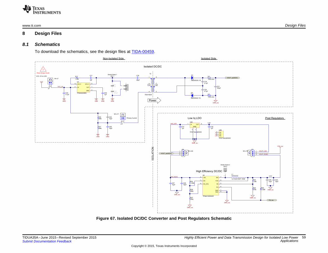
GND_iso
4.7µFC22
1µFC23
1.00k
R17
1µF
C17
10.0R19
DNP
22µF
C18
4.7µFC19
4.7µFC24
6.8µFC21
499kR20
499kR21
OUT1
IN2
CFLY-3
GND4
CFLY+5
U3
TPS60402DBV
10µFC25
10µFC26
12
J17
560pFC20DNP
SH-J17
GND GND GND GND
GNDGND
D7
RB520S30,115
D8
RB520S30,115
Primary Current
VCC: 3V to 3.6VSwitch Node 1
ISO
LA
TIO
N
!
Read Design Guide
VCC_IN
SW 1
GND1
VIN2
EN3
EN_HYS4
FB5
VOS6
SW7
PG8
PAD9
U4
TPS62125DSGR
10µFC30
10µFC29
10µFC28
10µFC27
GND_iso
GND_iso
GND_iso
L1
VLF302515MT-150M
PG_iso
2.00MR25
1.8MR22
576kR24
GND_iso
1.30MR23
499kR26
255kR27
GND_iso
IN1
7
OUT6
3
GND
U5A
TPS715A33DRVR NC2
NC4
NC5
U5B
TPS715A33DRVR
1µFC32
1
2
3
J191
2
3
J24SH-J19SH-J24
VCC_iso
GND_iso
1
J5
DNP
1
J6
DNP
1000 ohm
L2
1000 ohm
L3
1
2 7
8
3
4 5
6
T2
750315504
1µFC31
1 2
J7
VCC
SH-J7
1
J8
DNP
Non-Isolated Side Isolated Side
3.3V
3.3V
VOUT_isoDCDC
VOUT_isoDCDC
VIN_LDO
VIN_DCDC
VOUT_DCDC
VOUT_LDO
High Efficiency DC/DC
Switch Node 2SW 2
Low Iq LDO
Isolated DC/DC
Post Regulators
Power
www.ti.com Design Files
8 Design Files
8.1 SchematicsTo download the schematics, see the design files at TIDA-00459.
Figure 67. Isolated DC/DC Converter and Post Regulators Schematic
59TIDUA35A–June 2015–Revised September 2015 Highly Efficient Power and Data Transmission Design for Isolated Low PowerApplicationsSubmit Documentation Feedback
Copyright © 2015, Texas Instruments Incorporated
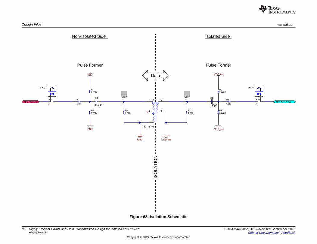
2.00MR1
2.00MR5
2.00MR2
2.00MR8
1.0k
R3
VCC VCC_iso
GND GND_iso
GND GND_iso
220pF
C1
220pF
C2
1 2
J1
1 2
J4
1
J2
DNP
1
J3
DNP
ISO_RX/TX ISO_RX/TX_iso
SH-J1 SH-J4
1.50kR6
1.0k
R4
1.50kR7
1
2
3
4
6T1
750315155
ISO
LA
TIO
N
Non-Isolated Side Isolated Side
Pulse Former Pulse Former
Data
Design Files www.ti.com
Figure 68. Isolation Schematic
60 Highly Efficient Power and Data Transmission Design for Isolated Low Power TIDUA35A–June 2015–Revised September 2015Applications Submit Documentation Feedback
Copyright © 2015, Texas Instruments Incorporated
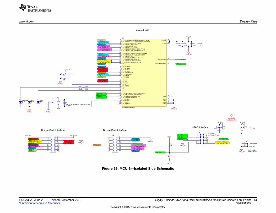
SH-J15
VCC_iso
47kR12
2200pFC9DNP
GND_iso
VCC_iso
VCC_TOOL_isoVCC_TARGET_iso
TEST_iso
RST_iso
P2.6_UCA1RXD_iso
P2.5_UCA1TXD_iso
10pF
C8
10pF
C7
GND_iso
GND_iso
0.1µFC6
GND_iso
10µFC5
0.1µFC4
10µFC3
GND_iso
GND_iso
VCC_iso
470R9470R10470R11
Super Red
21
D1Green
21
D2Yellow
21
D3
ISO_RX/TX_iso
ISO_RX_iso
ISO_TX_iso
ISO_RX_iso
ISO_TX_iso
GND_isoGND_iso
+5V_LP_iso
P1.7_UCB0SOMI_iso
P1.6_UCB0SIMO_iso
P1.4_SPI_CS_iso
1 2
S2
1 2
S3
1 2 3
J15
12
J16
VCC_iso
P1.5_SPI_CS_iso
P2.7_iso
P1.3_isoP3.0_iso
RST_iso
P1.0/TA0.1/DMAE0/RTCCLK/A0/C0/VREF-/VeREF-1
P1.1/TA0.2/TA1CLK/COUT/A1/C1/VREF+/VeREF+2
P1.2/TA1.1/TA0CLK/COUT/A2/C23
P3.0/A12/C124
P3.1/A13/C135
P3.2/A14/C146
P3.3/A15/C157
P4.78
P1.3/TA1.2/UCB0STE/A3/C39
P1.4/TB0.1/UCA0STE/A4/C410
P1.5/TB0.2/UCA0CLK/A5/C511
PJ.0/TDO/TB0OUTH/SMCLK/SRSCG1/C612
PJ.1/TDI/TCLK/MCLK/SRSCG0/C713
PJ.2/TMS/ACLK/SROSCOFF/C814
PJ.3/TCK/SRCPUOFF/C915
P4.0/A816
P4.1/A917
P4.2/A1018
P4.3/A1119
P2.5/TB0.0/UCA1TXD/UCA1SIMO20
P2.6/TB0.1/UCA1RXD/UCA1SOMI21
TEST/SBWTCK22
RST/NMI/SBWTDIO23
P2.0/TB0.6/UCA0TXD/UCA0SIMO/TB0CLK/ACLK24
P2.1/TB0.0/UCA0RXD/UCA0SOMI/TB0.025
P2.2/TB0.2/UCB0CLK26
P3.4/TB0.3/SMCLK27
P3.5/TB0.4/COUT28
P3.6/TB0.529
P3.7/TB0.630
P1.6/TB0.3/UCB0SIMO/UCB0SDA/TA0.031
P1.7/TB0.4/UCB0SOMI/UCB0SCL/TA1.032
P4.4/TB0.533
P4.534
P4.635
DVSS36
DVCC37
P2.738
P2.3/TA0.0/UCA1STE/A6/C1039
P2.4/TA1.0/UCA1CLK/A7/C1140
AVSS41
PJ.6/HFXIN42
PJ.7/HFXOUT43
AVSS44
PJ.4/LFXIN45
PJ.5/LFXOUT46
AVSS47
AVCC48
PAD49
U1
MSP430FR5969IRGZ
P2.2_UCB0CLK_iso
P1.7_UCB0SOMI_iso
P1.6_UCB0SIMO_iso
P1.4_SPI_CS_iso
P1.5_SPI_CS_iso
P1.3_iso
P3.0_iso
P2.7_iso
P2.3_iso
P2.4_iso
P3.1_A13_iso
P3.1_A13_iso
P2.3_iso
P2.4_iso
P3.2_A14_iso
P3.3_A15_iso
P4.1_A9_iso
P4.0_A8_iso
P4.1_A9_iso
P3.2_A14_iso
P3.3_A15_iso
P3.4_iso
P3.6_iso
P3.7_iso
P3.4_iso
P3.6_iso
P3.7_iso
1 2
S1
P2.5_UCA1TXD_iso
P2.6_UCA1RXD_iso
P2.5_UCA1TXD_iso
P2.6_UCA1RXD_iso
TDO_iso
TDI_iso
TMS_iso
TCK_iso
TDO_iso
TDI_iso
TMS_iso
TCK_iso
RST_iso
TEST_iso
GND_iso
32.768kHz12
Y1MS3V-T1R 32.768KHZ +/-20PPM 12.5PF
P4.0_A8_iso
P2.2_UCB0CLK_iso
1
2
3
J11
GND_iso
SH-J16
1
3
5 6
4
2
7
9 10
8
1211
1413
1615
1817
2019
J131
3
5 6
4
2
7
9 10
8
1211
1413
1615
1817
2019
J141 2
3 4
5 6
7 8
9 10
11 12
13 14
J9
PG_iso
Int Ext
ext_pwr_iso
GND_iso
Isolated Side
Read Design Guide
!
3.0V to 3.6VExternal Power
BoosterPack Interface BoosterPack Interface
JTAG Interface
www.ti.com Design Files
Figure 69. MCU 1—Isolated Side Schematic
61TIDUA35A–June 2015–Revised September 2015 Highly Efficient Power and Data Transmission Design for Isolated Low PowerApplicationsSubmit Documentation Feedback
Copyright © 2015, Texas Instruments Incorporated
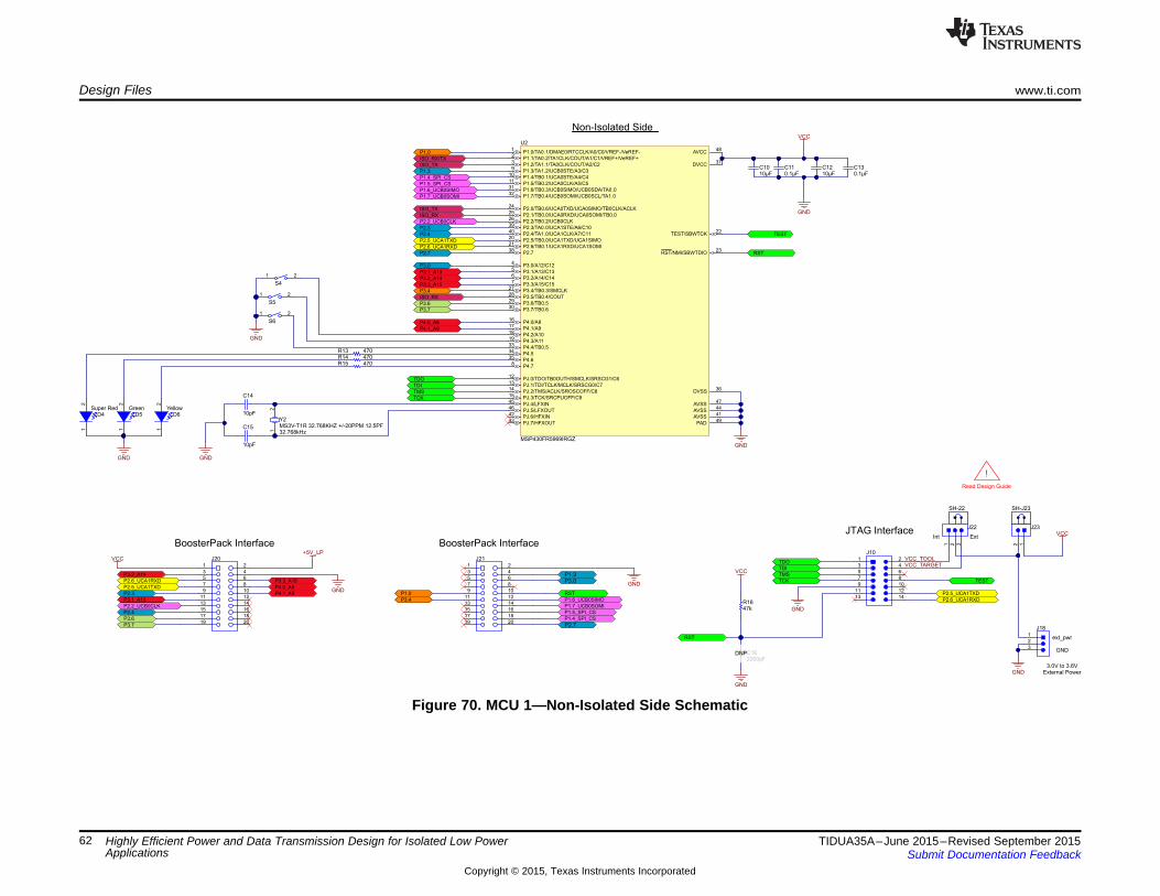
SH-22
VCC
47kR16
2200pFC16DNP
GND
VCC
VCC_TOOLVCC_TARGET
TEST
RST
P2.6_UCA1RXD
P2.5_UCA1TXD
10pF
C15
10pF
C14
GND
0.1µFC13
GND
10µFC12
0.1µFC11
10µFC10
GND
GND
VCC
470R13470R14470R15
Super Red
21
D4Green
21
D5Yellow
21
D6
ISO_RX/TX
ISO_RX
ISO_TX
ISO_RX
ISO_TX
GNDGND
+5V_LP
P1.7_UCB0SOMI
P1.6_UCB0SIMO
P1.4_SPI_CS
1 2
S5
1 2
S6
1 2 3
J22
12
J23
VCC
P1.5_SPI_CS
P2.7
P1.3P3.0
RST
P1.0/TA0.1/DMAE0/RTCCLK/A0/C0/VREF-/VeREF-1
P1.1/TA0.2/TA1CLK/COUT/A1/C1/VREF+/VeREF+2
P1.2/TA1.1/TA0CLK/COUT/A2/C23
P3.0/A12/C124
P3.1/A13/C135
P3.2/A14/C146
P3.3/A15/C157
P4.78
P1.3/TA1.2/UCB0STE/A3/C39
P1.4/TB0.1/UCA0STE/A4/C410
P1.5/TB0.2/UCA0CLK/A5/C511
PJ.0/TDO/TB0OUTH/SMCLK/SRSCG1/C612
PJ.1/TDI/TCLK/MCLK/SRSCG0/C713
PJ.2/TMS/ACLK/SROSCOFF/C814
PJ.3/TCK/SRCPUOFF/C915
P4.0/A816
P4.1/A917
P4.2/A1018
P4.3/A1119
P2.5/TB0.0/UCA1TXD/UCA1SIMO20
P2.6/TB0.1/UCA1RXD/UCA1SOMI21
TEST/SBWTCK22
RST/NMI/SBWTDIO23
P2.0/TB0.6/UCA0TXD/UCA0SIMO/TB0CLK/ACLK24
P2.1/TB0.0/UCA0RXD/UCA0SOMI/TB0.025
P2.2/TB0.2/UCB0CLK26
P3.4/TB0.3/SMCLK27
P3.5/TB0.4/COUT28
P3.6/TB0.529
P3.7/TB0.630
P1.6/TB0.3/UCB0SIMO/UCB0SDA/TA0.031
P1.7/TB0.4/UCB0SOMI/UCB0SCL/TA1.032
P4.4/TB0.533
P4.534
P4.635
DVSS36
DVCC37
P2.738
P2.3/TA0.0/UCA1STE/A6/C1039
P2.4/TA1.0/UCA1CLK/A7/C1140
AVSS41
PJ.6/HFXIN42
PJ.7/HFXOUT43
AVSS44
PJ.4/LFXIN45
PJ.5/LFXOUT46
AVSS47
AVCC48
PAD49
U2
MSP430FR5969IRGZ
P2.2_UCB0CLK
P1.7_UCB0SOMI
P1.6_UCB0SIMO
P1.4_SPI_CS
P1.5_SPI_CS
P1.3
P3.0
P2.7
P2.3
P2.4
P3.1_A13
P3.1_A13
P2.3
P2.4
P3.2_A14
P3.3_A15
P4.1_A9
P4.0_A8
P4.1_A9
P3.2_A14
P3.3_A15
P1.0
P3.4
P3.6
P3.7
P1.0
P3.4
P3.6
P3.7
1 2
S4
P2.5_UCA1TXD
P2.6_UCA1RXD
P2.5_UCA1TXD
P2.6_UCA1RXD
TDO
TDI
TMS
TCK
TDO
TDI
TMS
TCK
RST
TEST
GND
32.768kHz12
Y2MS3V-T1R 32.768KHZ +/-20PPM 12.5PF
P4.0_A8
P2.2_UCB0CLK
1
2
3
J18
GND
GND
SH-J23
1
3
5 6
4
2
7
9 10
8
1211
1413
1615
1817
2019
J201
3
5 6
4
2
7
9 10
8
1211
1413
1615
1817
2019
J21 1 2
3 4
5 6
7 8
9 10
11 12
13 14
J10
Int Ext
ext_pwr
GND
Non-Isolated Side
Read Design Guide
!
3.0V to 3.6VExternal Power
BoosterPack Interface BoosterPack Interface
JTAG Interface
Design Files www.ti.com
Figure 70. MCU 1—Non-Isolated Side Schematic
space
space
62 Highly Efficient Power and Data Transmission Design for Isolated Low Power TIDUA35A–June 2015–Revised September 2015Applications Submit Documentation Feedback
Copyright © 2015, Texas Instruments Incorporated

www.ti.com Design Files
8.2 Bill of MaterialsTo download the bill of materials (BOM), see the design files at TIDA-00459.
Table 15. BOM
PACKAGEITEM DESIGNATOR QTY VALUE PARTNUMBER MANUFACTURER DESCRIPTION REFERENCE1 !PCB1 1 TIDA-00459 Any Printed Circuit Board
CAP, CERM, 220 pF, 50 V, +/- 5%,2 C1, C2 2 220pF C1608C0G1H221J TDK 0603C0G/NP0, 0603C3, C5, C10, C12, CAP, CERM, 10 µF, 16 V, +/- 10%,3 8 10uF GRM21BR61C106KE15L MuRata 0805C27, C28, C29, C30 X5R, 0805
CAP, CERM, 0.1 µF, 10 V, +/- 10%,4 C4, C6, C11, C13 4 0.1uF GRM155R71A104KA01D MuRata 0402X7R, 0402CAP, CERM, 10 pF, 50 V, +/- 5%,5 C7, C8, C14, C15 4 10pF GRM1555C1H100JA01D MuRata 0402C0G/NP0, 0402CAP, CERM, 1uF, 10V, +/-10%,6 C17 1 1uF GRM155R61A105KE15D MuRata 0402X5R, 0402CAP, CERM, 22uF, 10V, +/-10%,7 C18 1 22uF GRM31CR61A226KE19L MuRata 1206X5R, 1206CAP, CERM, 4.7 µF, 10 V, +/- 10%,8 C19, C24 2 4.7uF CGB3B1X5R1A475K055AC TDK 0603X5R, 0603CAP, CERM, 6.8 µF, 25 V, +/- 10%,9 C21 1 6.8uF C1608X5R1E685K080AC TDK 0603X5R, 0603CAP, CERM, 4.7uF, 10V, +/-10%,10 C22 1 4.7uF C0603C475K8PACTU Kemet 0603X5R, 0603CAP, CERM, 1uF, 10V, +/-10%,11 C23 1 1uF GRM188R71A105KA61D MuRata 0603X7R, 0603CAP, CERM, 10uF, 10V, +/-10%,12 C25, C26 2 10uF GRM21BR71A106KE51L MuRata 0805X7R, 0805CAP, CERM, 1 µF, 16 V, +/- 10%,13 C31 1 1uF GRM188R61C105KA93D MuRata 0603X5R, 0603CAP, CERM, 1 µF, 10 V, +/- 10%,14 C32 1 1uF GRM188R61A105KA61D MuRata 0603X5R, 0603
15 D1, D4 2 Super Red 150060SS75000 Wurth Elektronik eiSos LED, Super Red, SMD LED_060316 D2, D5 2 Green 150060VS75000 Wurth Elektronik eiSos LED, Green, SMD LED_060317 D3, D6 2 Yellow 150060YS75000 Wurth Elektronik eiSos LED, Yellow, SMD LED_0603
Diode, Schottky, 30 V, 0.2 A, SOD-18 D7, D8 2 30V RB520S30,115 NXP Semiconductor SOD-523523J1, J4, J7, J16, J17, Header, 2.54mm, 2x1,19 6 61300211121 Wurth Elektronik Header, 2.54 mm, 2x1, Gold, THJ23 TH
63TIDUA35A–June 2015–Revised September 2015 Highly Efficient Power and Data Transmission Design for Isolated Low PowerApplicationsSubmit Documentation Feedback
Copyright © 2015, Texas Instruments Incorporated

Design Files www.ti.com
Table 15. BOM (continued)PACKAGEITEM DESIGNATOR QTY VALUE PARTNUMBER MANUFACTURER DESCRIPTION REFERENCE
Header (Shrouded), 2.54 mm, 7x2, Header (Shrouded),20 J9, J10 2 SBH11-PBPC-D07-RA-BK Sullins Connector Solutions Gold, R/A, TH 2.54 mm, 7x2, R/A, TH21 J11, J18 2 TSW-103-08-G-S-RA Samtec Header, 100mil, 3x1, Gold, R/A, TH 3x1 R/A Header
Connector, Receptacle, 100mil,22 J13, J14, J20, J21 4 SSW-110-23-F-D Samtec 10x2 Receptacle10x2, Gold plated, THHeader, 2.54mm, 3x1,23 J15, J19, J22, J24 4 61300311121 Wurth Elektronik Header, 2.54 mm, 3x1, Gold, TH TH
Inductor, Shielded, Ferrite, 15 µH,24 L1 1 15uH VLF302515MT-150M TDK IND_3x1.5x3mm0.56 A, 0.275 ohm, SMDFerrite Bead, 1000 ohm @ 10025 L2, L3 2 1000 ohm 742792662 Wurth Elektronik 0603MHz, 0.6 A, 0603
26 R1, R2, R5, R8, R25 5 2.00Meg CRCW06032M00FKEA Vishay-Dale RES, 2.00 M, 1%, 0.1 W, 0603 060327 R3, R4 2 1.0k CRCW06031K00JNEA Vishay-Dale RES, 1.0 k, 5%, 0.1 W, 0603 060328 R6, R7 2 1.50k CRCW06031K50FKEA Vishay-Dale RES, 1.50 k, 1%, 0.1 W, 0603 0603
R9, R10, R11, R13,29 6 470 CRCW0402470RJNED Vishay-Dale RES, 470, 5%, 0.063 W, 0402 0402R14, R1530 R12, R16 2 47k CRCW040247K0JNED Vishay-Dale RES, 47 k, 5%, 0.063 W, 0402 040231 R17 1 1.00k CRCW04021K00FKED Vishay-Dale RES, 1.00k ohm, 1%, 0.063W, 0402 040232 R20, R21 2 499k CRCW0402499KFKED Vishay-Dale RES, 499k ohm, 1%, 0.063W, 0402 040233 R22 1 1.8Meg CRCW06031M80FKEA Vishay-Dale RES, 1.8 M, 1%, 0.1 W, 0603 060334 R23 1 1.30Meg CRCW06031M30FKEA Vishay-Dale RES, 1.30 M, 1%, 0.1 W, 0603 060335 R24 1 576k CRCW0603576KFKEA Vishay-Dale RES, 576 k, 1%, 0.1 W, 0603 060336 R26 1 499k CRCW0603499KFKEA Vishay-Dale RES, 499 k, 1%, 0.1 W, 0603 060337 R27 1 255k CRCW0603255KFKEA Vishay-Dale RES, 255 k, 1%, 0.1 W, 0603 0603
S1, S2, S3, S4, S5,38 6 434121025816 Wurth Elektronik eiSos Switch, Tactile, SPST, 12 V, SMD SMD, 6x3.9mmS6SH-22, SH-J1, SH-J4, SH-J7, SH-J15,
39 SH-J16, SH-J17, 10 1x2 969102-0000-DA 3M Shunt, 100mil, Gold plated, Black ShuntSH-J19, SH-J23,SH-J24
SMD, Body40 T1 1 400 uH 750315155 Wurth Elektronik eiSos Transformer, 400 uH, SMT 8.26x6.6mm41 T2 1 1.8 mH 750315504 Wurth Elektronik Transformer, 1.8 mH, SMT 8.38x7.87mm
Mixed Signal Microcontroller,42 U1, U2 2 MSP430FR5969IRGZ Texas Instruments RGZ0048BRGZ0048B
64 Highly Efficient Power and Data Transmission Design for Isolated Low Power TIDUA35A–June 2015–Revised September 2015Applications Submit Documentation Feedback
Copyright © 2015, Texas Instruments Incorporated

www.ti.com Design Files
Table 15. BOM (continued)PACKAGEITEM DESIGNATOR QTY VALUE PARTNUMBER MANUFACTURER DESCRIPTION REFERENCE
UNREGULATED 60-mA CHARGE43 U3 1 TPS60402DBV Texas Instruments PUMP VOLTAGE INVERTER, DBV0005A
DBV0005A3V-17V, 300mA Step DownConverter With Adjustable Enable44 U4 1 TPS62125DSGR Texas Instruments DSG0008AThreshold And Hysteresis,DSG0008ASingle Output LDO, 80 mA, Fixed3.3 V Output, 2.5 to 24 V Input, with45 U5 1 TPS715A33DRVR Texas Instruments DRV0006ALow IQ, 6-pin SON (DRV), -40 to 85degC, Green (RoHS & no Sb/Br)
MS3V-T1R 32.768KHZ +/-46 Y1, Y2 2 Micro Crystal AG Crystal, 32.768kHz, 12.5pF, SMD 1.4x1.4x5.0mm SMD20PPM 12.5PFCAP, CERM, 2200 pF, 6.3 V, +/-47 C9, C16 0 2200pF GRM155R70J222KA01D MuRata 040210%, X7R, 0402CAP, CERM, 560pF, 50V, +/-10%,48 C20 0 560pF GRM155R71H561KA01D MuRata 0402X7R, 0402Fiducial mark. There is nothing to49 FID1, FID2, FID3 0 N/A N/A N/Abuy or mount.Machine Screw, Round, #4-40 x 1/4,50 H1, H2, H3, H4 0 NY PMS 440 0025 PH B&F Fastener Supply ScrewNylon, Philips panhead
51 H5, H6, H7, H8 0 1902C Keystone Standoff, Hex, 0.5"L #4-40 Nylon StandoffHeader, 2.54 mm, 1x1,52 J2, J3, J5, J6, J8 0 61300111121 Wurth Elektronik Header, 2.54 mm, 1x1, Gold, TH TH
53 R19 0 10.0 CRCW040210R0FKED Vishay-Dale RES, 10.0 ohm, 1%, 0.063W, 0402 0402
65TIDUA35A–June 2015–Revised September 2015 Highly Efficient Power and Data Transmission Design for Isolated Low PowerApplicationsSubmit Documentation Feedback
Copyright © 2015, Texas Instruments Incorporated
Design Files www.ti.com
8.3 PCB Layout RecommendationsThe TIDA-00459 board has the form factor of a LaunchPad. A LaunchPad is an easy-to-use developmenttool intended for beginners and experienced users alike for creating microcontroller-based applications.For the LaunchPad, there are BoosterPack plug-in boards available to expand the LaunchPad'sfunctionality. BoosterPack plug-in modules (www.ti.com/boosterpack) allow the user to add features likewireless connectivity, capacitive touch, temperature sensing, displays, and much more.
To create a BoosterPack for specific needs, use the resources found athttp://www.ti.com/ww/en/launchpad/byob.html to create your BoosterPack design files, get support fromour community, and take your idea from concept to PCB to product in a few easy steps.
8.3.1 Layer PlotsTo download the layer plots, see the design files at TIDA-00459.
8.4 Altium ProjectTo download the Altium project files, see the design files at TIDA-00459.
8.5 Gerber FilesTo download the Gerber files, see the design files at TIDA-00459.
8.6 Assembly DrawingsTo download the assembly drawings, see the design files at TIDA-00459.
66 Highly Efficient Power and Data Transmission Design for Isolated Low Power TIDUA35A–June 2015–Revised September 2015Applications Submit Documentation Feedback
Copyright © 2015, Texas Instruments Incorporated

www.ti.com Software Files
9 Software FilesTo download the software files, see the design files at TIDA-00459.
10 References
1. Texas Instruments, SN6501 Transformer Driver for Isolated Power Supplies, SN6501 Datasheet,(SLLSEA0)
2. Texas Instruments, TPS715A, 24-V High Input Voltage, Micropower, 80-mA LDO Voltage Regulator,TPS715A Datasheet; (SBVS047)
3. Texas Instruments, TPS62125, 3-V to 17-V, 300-mA Step-Down Converter With Adjustable EnableThreshold and Hysteresis, TPS62125 Datasheet; (SLVSAQ5)
4. Texas Instruments, MSP430FR59xx Mixed-Signal Microcontrollers, MSP430FR5969 Datasheet(SLAS704)
5. Texas Instruments, MSP430FR58xx, MSP430FR59xx, MSP430FR68xx, and MSP430FR69xx FamilyUser's Guide, MSP430FR5969 User's Guide (SLAU367)
6. Texas Instruments, TPS6040x Unregulated 60-mA Charge Pump Voltage Inverter, TPS60402Datasheet (SLVS324)
7. Texas Instruments, Uniquely Efficient Isolated DC/DC Converter for Ultra-Low Power and Low-PowerApplications, TIDA-00349 Reference Design (TIDU813)
8. Texas Instruments, Isolated, Ultra-Low Power Design for 4- to 20-mA Loop-Powered Transmitters,TIDA-00167 Reference Guide (TIDU414)
9. Texas Instruments, Magnetics Design for Switching Power Supplies, Design Handbook (SLUP123)10. Würth Elektronik, Power Transformer Spec Sheet 50315504 (PDF)
11 About the AuthorTHOMAS SCHNEIDER is a Systems Engineer at Texas Instruments where he is responsible fordeveloping reference design solutions for the industrial segment. Thomas brings to this role his wideexperience in TI microcontrollers, especially MSP430. Thomas earned his Dipl.-Ing. (Univ.) degree inelectrical engineering from the Technical University Munich (TUM) in Munich, Germany.
JÜERGEN SCHNEIDER is a Systems Engineer at Texas Instruments where he is responsible fordeveloping TI Designs for the industrial automation segment. He holds a Dipl.-Ing. (FH) degree inindustrial electronics and has worked 13 years as a design engineer for semiconductor manufacturingequipment, telemetry systems, and electro-medical devices before joining TI in 1999. Jüergen has workedwith TI as an analog field specialist, FAE, and systems engineer for power solutions. He presents attechnical conferences and seminars and has been one of the presenters of the industry-wide known TIPower Supply Design Seminar for multiple years. Jüergen also has the distinguishment of being electedas a Member, Group Technical Staff.
67TIDUA35A–June 2015–Revised September 2015 Highly Efficient Power and Data Transmission Design for Isolated Low PowerApplicationsSubmit Documentation Feedback
Copyright © 2015, Texas Instruments Incorporated

Revision History www.ti.com
Revision History
Changes from Original (June 2015) to A Revision ......................................................................................................... Page
• Changed from preview page............................................................................................................. 1
NOTE: Page numbers for previous revisions may differ from page numbers in the current version.
68 Revision History TIDUA35A–June 2015–Revised September 2015Submit Documentation Feedback
Copyright © 2015, Texas Instruments Incorporated

IMPORTANT NOTICE FOR TI REFERENCE DESIGNS
Texas Instruments Incorporated ("TI") reference designs are solely intended to assist designers (“Buyers”) who are developing systems thatincorporate TI semiconductor products (also referred to herein as “components”). Buyer understands and agrees that Buyer remainsresponsible for using its independent analysis, evaluation and judgment in designing Buyer’s systems and products.TI reference designs have been created using standard laboratory conditions and engineering practices. TI has not conducted anytesting other than that specifically described in the published documentation for a particular reference design. TI may makecorrections, enhancements, improvements and other changes to its reference designs.Buyers are authorized to use TI reference designs with the TI component(s) identified in each particular reference design and to modify thereference design in the development of their end products. HOWEVER, NO OTHER LICENSE, EXPRESS OR IMPLIED, BY ESTOPPELOR OTHERWISE TO ANY OTHER TI INTELLECTUAL PROPERTY RIGHT, AND NO LICENSE TO ANY THIRD PARTY TECHNOLOGYOR INTELLECTUAL PROPERTY RIGHT, IS GRANTED HEREIN, including but not limited to any patent right, copyright, mask work right,or other intellectual property right relating to any combination, machine, or process in which TI components or services are used.Information published by TI regarding third-party products or services does not constitute a license to use such products or services, or awarranty or endorsement thereof. Use of such information may require a license from a third party under the patents or other intellectualproperty of the third party, or a license from TI under the patents or other intellectual property of TI.TI REFERENCE DESIGNS ARE PROVIDED "AS IS". TI MAKES NO WARRANTIES OR REPRESENTATIONS WITH REGARD TO THEREFERENCE DESIGNS OR USE OF THE REFERENCE DESIGNS, EXPRESS, IMPLIED OR STATUTORY, INCLUDING ACCURACY ORCOMPLETENESS. TI DISCLAIMS ANY WARRANTY OF TITLE AND ANY IMPLIED WARRANTIES OF MERCHANTABILITY, FITNESSFOR A PARTICULAR PURPOSE, QUIET ENJOYMENT, QUIET POSSESSION, AND NON-INFRINGEMENT OF ANY THIRD PARTYINTELLECTUAL PROPERTY RIGHTS WITH REGARD TO TI REFERENCE DESIGNS OR USE THEREOF. TI SHALL NOT BE LIABLEFOR AND SHALL NOT DEFEND OR INDEMNIFY BUYERS AGAINST ANY THIRD PARTY INFRINGEMENT CLAIM THAT RELATES TOOR IS BASED ON A COMBINATION OF COMPONENTS PROVIDED IN A TI REFERENCE DESIGN. IN NO EVENT SHALL TI BELIABLE FOR ANY ACTUAL, SPECIAL, INCIDENTAL, CONSEQUENTIAL OR INDIRECT DAMAGES, HOWEVER CAUSED, ON ANYTHEORY OF LIABILITY AND WHETHER OR NOT TI HAS BEEN ADVISED OF THE POSSIBILITY OF SUCH DAMAGES, ARISING INANY WAY OUT OF TI REFERENCE DESIGNS OR BUYER’S USE OF TI REFERENCE DESIGNS.TI reserves the right to make corrections, enhancements, improvements and other changes to its semiconductor products and services perJESD46, latest issue, and to discontinue any product or service per JESD48, latest issue. Buyers should obtain the latest relevantinformation before placing orders and should verify that such information is current and complete. All semiconductor products are soldsubject to TI’s terms and conditions of sale supplied at the time of order acknowledgment.TI warrants performance of its components to the specifications applicable at the time of sale, in accordance with the warranty in TI’s termsand conditions of sale of semiconductor products. Testing and other quality control techniques for TI components are used to the extent TIdeems necessary to support this warranty. Except where mandated by applicable law, testing of all parameters of each component is notnecessarily performed.TI assumes no liability for applications assistance or the design of Buyers’ products. Buyers are responsible for their products andapplications using TI components. To minimize the risks associated with Buyers’ products and applications, Buyers should provideadequate design and operating safeguards.Reproduction of significant portions of TI information in TI data books, data sheets or reference designs is permissible only if reproduction iswithout alteration and is accompanied by all associated warranties, conditions, limitations, and notices. TI is not responsible or liable forsuch altered documentation. Information of third parties may be subject to additional restrictions.Buyer acknowledges and agrees that it is solely responsible for compliance with all legal, regulatory and safety-related requirementsconcerning its products, and any use of TI components in its applications, notwithstanding any applications-related information or supportthat may be provided by TI. Buyer represents and agrees that it has all the necessary expertise to create and implement safeguards thatanticipate dangerous failures, monitor failures and their consequences, lessen the likelihood of dangerous failures and take appropriateremedial actions. Buyer will fully indemnify TI and its representatives against any damages arising out of the use of any TI components inBuyer’s safety-critical applications.In some cases, TI components may be promoted specifically to facilitate safety-related applications. With such components, TI’s goal is tohelp enable customers to design and create their own end-product solutions that meet applicable functional safety standards andrequirements. Nonetheless, such components are subject to these terms.No TI components are authorized for use in FDA Class III (or similar life-critical medical equipment) unless authorized officers of the partieshave executed an agreement specifically governing such use.Only those TI components that TI has specifically designated as military grade or “enhanced plastic” are designed and intended for use inmilitary/aerospace applications or environments. Buyer acknowledges and agrees that any military or aerospace use of TI components thathave not been so designated is solely at Buyer's risk, and Buyer is solely responsible for compliance with all legal and regulatoryrequirements in connection with such use.TI has specifically designated certain components as meeting ISO/TS16949 requirements, mainly for automotive use. In any case of use ofnon-designated products, TI will not be responsible for any failure to meet ISO/TS16949.IMPORTANT NOTICE
Mailing Address: Texas Instruments, Post Office Box 655303, Dallas, Texas 75265Copyright © 2015, Texas Instruments Incorporated