hoffman lab microscopes - harvard...
TRANSCRIPT

Scanning Tunneling Microscope
Ultra-high vacuum STM
Force Microscope
Hoffman Lab Microscopes
NdFeAsO1-xFx VO2 Nd2Fe14B
Bi-2212
PrxCa1-xFe2As2
Bi-2201 Ba(Fe1-xCox)2As2
Bi2Se3
NbSe2
Sb(111)
2 nm
Li0.9Mo6O17
SmB6
KxSr1-xFe2As2
Ca-YBCO

Jenny Hoffman
Nanoscale Imaging of Topological Materials: Sb and SmB6
Funding:
Experiments:
(Harvard)
Samples: Sb: Dillon Gardner, Young Lee SmB6: Dae-Jeong Kim, Zach Fisk
Theory: Hsin Lin, Arun Bansil Jay Sau, Anton Akhmerov, Bert Halperin
Anjan Soumyanarayanan
Mike Yee Yang He Jason Zhu

Outline
3
• Topological Insulators
• Scanning Tunneling Microscopy
• Nanoscale Band Structure • Topological: Sb
• Insulator: SmB6
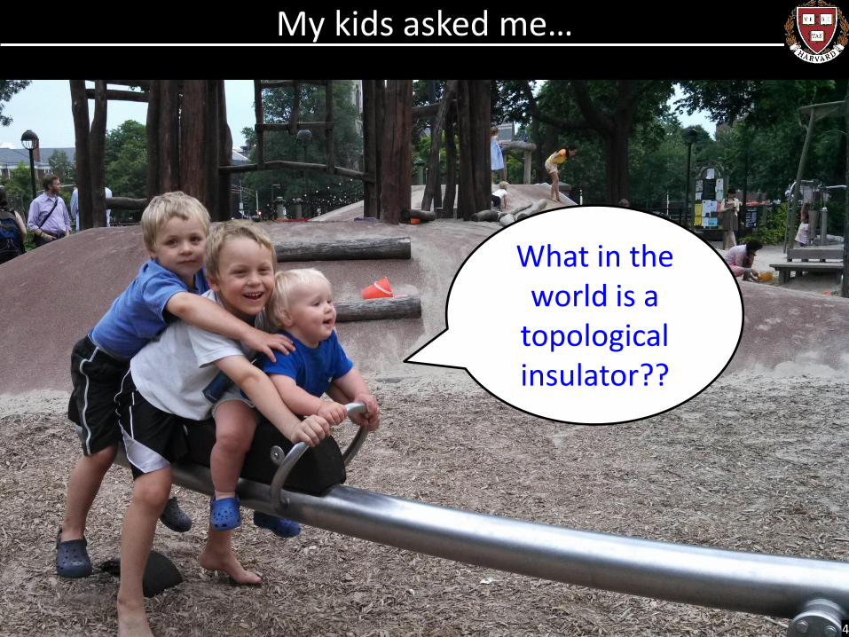
My kids asked me…
What in the world is a
topological insulator??
4

A topological insulator is a material with…
insulating bulk
conducting surface
But what makes it
topological?
5

Band Theory
Single atom:
1s
2s
2p
3s
E
Crystal:
6
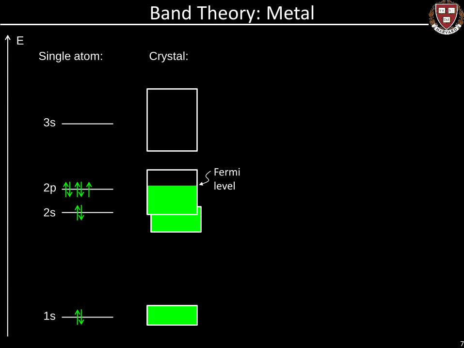
Band Theory: Metal
Single atom:
1s
2s
2p
3s
E
Crystal:
Fermi level
7
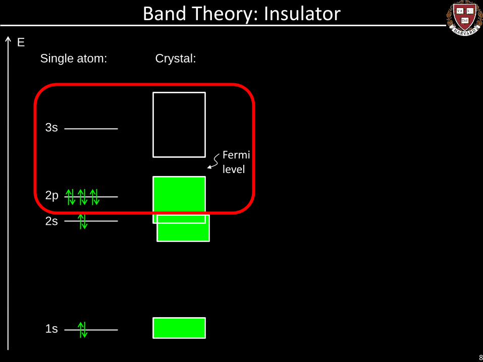
Band Theory: Insulator
Single atom:
1s
2s
2p
3s
E
Crystal:
Fermi level
8

Spin-Orbit Coupling
9
Material Vacuum
𝜀𝐹
Ener
gy
p3/2
s
Vacuum
Band gap: 2𝑚𝑒𝑐2~ 106 eV
→ Band Inversion

Spin-Orbit Coupling
10
Material Vacuum Vacuum
𝜀𝐹
Ener
gy
p3/2
s
Metallic surface states
→ topologically protected spin-polarized surface states
Why spin-polarized?
Band gap: 2𝑚𝑒𝑐2~ 106 eV
→ Band Inversion

Band Theory: Insulator
Single atom:
1s
2s
2p
3s
E
Crystal: Add momentum information:
k
E
Brillouin zone edge
Fermi level
11

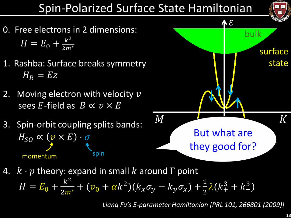
Spin-Polarized Surface State Hamiltonian 𝜀
12
𝑘
bulk

Spin-Polarized Surface State Hamiltonian 𝜀
13
𝑘
bulk
surface state
0. Free electrons in 2 dimensions:
𝐻 = 𝐸0 + 𝑘2
2𝑚∗
1. Rashba: Surface breaks symmetry 𝐻𝑅 = 𝐸𝑧
2. Moving electron with velocity 𝑣 sees 𝐸-field as 𝐵 ∝ 𝑣 × 𝐸

14
𝜀
𝑘
bulk
surface state
Spin-Polarized Surface State Hamiltonian
0. Free electrons in 2 dimensions:
𝐻 = 𝐸0 + 𝑘2
2𝑚∗
1. Rashba: Surface breaks symmetry 𝐻𝑅 = 𝐸𝑧
2. Moving electron with velocity 𝑣 sees 𝐸-field as 𝐵 ∝ 𝑣 × 𝐸
3. Spin-orbit coupling splits bands: 𝐻𝑆𝑂 ∝ 𝑣 × 𝐸 ⋅ 𝜎 momentum spin
𝐻𝑆𝑂 ∝ 𝑣 × 𝐸 ⋅ 𝜎

15
𝜀 bulk
surface state
𝑘
Spin-Polarized Surface State Hamiltonian
0. Free electrons in 2 dimensions:
𝐻 = 𝐸0 + 𝑘2
2𝑚∗
1. Rashba: Surface breaks symmetry 𝐻𝑅 = 𝐸𝑧
2. Moving electron with velocity 𝑣 sees 𝐸-field as 𝐵 ∝ 𝑣 × 𝐸
3. Spin-orbit coupling splits bands: 𝐻𝑆𝑂 ∝ 𝑣 × 𝐸 ⋅ 𝜎 4. 𝑘 ⋅ 𝑝 theory: expand in small 𝑘 around Γ point
𝐻 = 𝐸0 +𝑘2
2𝑚∗ + 𝑣(𝑘𝑥𝜎𝑦 − 𝑘𝑦𝜎𝑥)
momentum spin
𝐻𝑆𝑂 ∝ 𝑣 × 𝐸 ⋅ 𝜎

16
𝜀
surface state
𝑘
bulk 0. Free electrons in 2 dimensions:
𝐻 = 𝐸0 + 𝑘2
2𝑚∗
1. Rashba: Surface breaks symmetry 𝐻𝑅 = 𝐸𝑧
2. Moving electron with velocity 𝑣 sees 𝐸-field as 𝐵 ∝ 𝑣 × 𝐸
3. Spin-orbit coupling splits bands: 𝐻𝑆𝑂 ∝ 𝑣 × 𝐸 ⋅ 𝜎 4. 𝑘 ⋅ 𝑝 theory: expand in small 𝑘 around Γ point
𝐻 = 𝐸𝐷 +𝑘2
2𝑚∗ + 𝑣(𝑘𝑥𝜎𝑦 − 𝑘𝑦𝜎𝑥) 𝐻 = 𝐸0 +𝑘2
2𝑚∗ + (𝑣0 + 𝛼𝑘2)(𝑘𝑥𝜎𝑦 − 𝑘𝑦𝜎𝑥)
Spin-Polarized Surface State Hamiltonian
new term to bend band down
momentum spin
𝐻𝑆𝑂 ∝ 𝑣 × 𝐸 ⋅ 𝜎

17
𝜀 bulk
𝐾 𝑀
surface state
0. Free electrons in 2 dimensions:
𝐻 = 𝐸0 + 𝑘2
2𝑚∗
1. Rashba: Surface breaks symmetry 𝐻𝑅 = 𝐸𝑧
2. Moving electron with velocity 𝑣 sees 𝐸-field as 𝐵 ∝ 𝑣 × 𝐸
3. Spin-orbit coupling splits bands: 𝐻𝑆𝑂 ∝ 𝑣 × 𝐸 ⋅ 𝜎 4. 𝑘 ⋅ 𝑝 theory: expand in small 𝑘 around Γ point
𝐻 = 𝐸𝐷 +𝑘2
2𝑚∗ + 𝑣(𝑘𝑥𝜎𝑦 − 𝑘𝑦𝜎𝑥)
momentum spin
𝐻𝑆𝑂 ∝ 𝑣 × 𝐸 ⋅ 𝜎
𝐻 = 𝐸0 +𝑘2
2𝑚∗ + (𝑣0 + 𝛼𝑘2)(𝑘𝑥𝜎𝑦 − 𝑘𝑦𝜎𝑥) +1
2𝜆(𝑘+
3 + 𝑘−3 )
crystal symmetry
Spin-Polarized Surface State Hamiltonian
18
𝜀 bulk
𝐾 𝑀
surface state
0. Free electrons in 2 dimensions:
𝐻 = 𝐸0 + 𝑘2
2𝑚∗
1. Rashba: Surface breaks symmetry 𝐻𝑅 = 𝐸𝑧
2. Moving electron with velocity 𝑣 sees 𝐸-field as 𝐵 ∝ 𝑣 × 𝐸
3. Spin-orbit coupling splits bands: 𝐻𝑆𝑂 ∝ 𝑣 × 𝐸 ⋅ 𝜎 4. 𝑘 ⋅ 𝑝 theory: expand in small 𝑘 around Γ point
𝐻 = 𝐸𝐷 +𝑘2
2𝑚∗ + 𝑣(𝑘𝑥𝜎𝑦 − 𝑘𝑦𝜎𝑥)
momentum spin
𝐻𝑆𝑂 ∝ 𝑣 × 𝐸 ⋅ 𝜎
𝐻 = 𝐸0 +𝑘2
2𝑚∗ + (𝑣0 + 𝛼𝑘2)(𝑘𝑥𝜎𝑦 − 𝑘𝑦𝜎𝑥) +1
2𝜆(𝑘+
3 + 𝑘−3 )
crystal symmetry
𝐻 = 𝐸0 +𝑘2
2𝑚∗ + (𝑣0 + 𝛼𝑘2)(𝑘𝑥𝜎𝑦 − 𝑘𝑦𝜎𝑥) +1
2𝜆(𝑘+
3 + 𝑘−3 )
Liang Fu’s 5-parameter Hamiltonian [PRL 101, 266801 (2009)]
But what are they good for?
Spin-Polarized Surface State Hamiltonian

Applications of Topological Insulators
1. Spintronics
2. Topological quantum computing
𝑡
Majorana fermion = self-antiparticle (non-Abelian anyon)
“braid” the world-lines → information is encoded topologically
Topological-superconductor interface
19
How can we realize these applications?
Fu & Kane, PRL 100, 096407 (2008)
SC
proximity ½ triplet: (↑↓+↓↑)/ 𝟐 TI
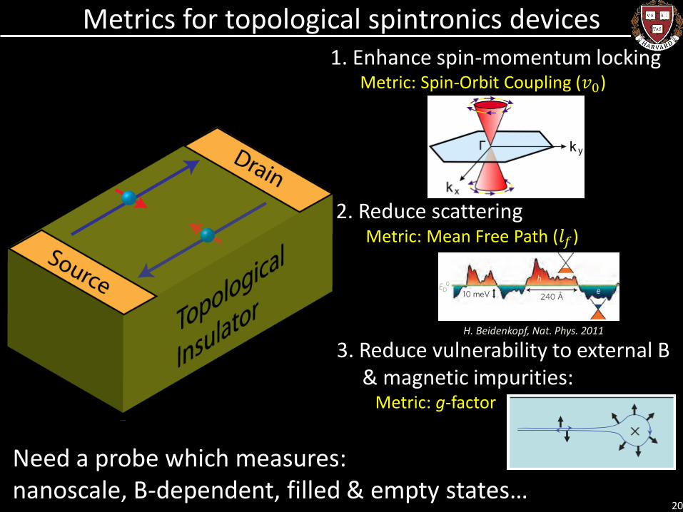
Metrics for topological spintronics devices
20
Need a probe which measures: nanoscale, B-dependent, filled & empty states…
1. Enhance spin-momentum locking Metric: Spin-Orbit Coupling (𝑣0)
3. Reduce vulnerability to external B & magnetic impurities:
Metric: g-factor
H. Beidenkopf, Nat. Phys. 2011
2. Reduce scattering Metric: Mean Free Path (𝑙𝑓)
Outline
21
• Topological Insulators
• Scanning Tunneling Microscopy
• Nanoscale Band Structure • Topological: Sb
• Insulator: SmB6

Scanning Tunneling Microscopy
E
EF (sample) EF (tip)
Sample LDOS under tip
TIP DOS
vacuum
E
GW Tip
Sample
V
Tip
Sample
22

E
EF (sample)
EF (tip)
Sample LDOS under tip
TIP DOS
vacuum
E
GW Tip
Sample
V
Tip
Sample
Scanning Tunneling Microscopy
( ) LDOS( )
F
eV
E
I V E dE
23

Types of STM Measurements
Local Density of
States (x, y, E)
Constant
current
mode:
Topography
dI/dV Spectrum
dI/dV Map x y
E
dI
dV24
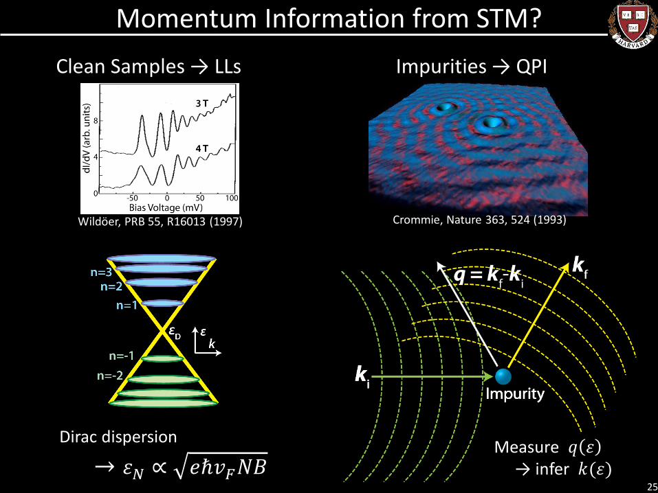
Momentum Information from STM?
Crommie, Nature 363, 524 (1993)
Impurities → QPI
Wildöer, PRB 55, R16013 (1997)
Clean Samples → LLs
25
Measure 𝑞 𝜀 → infer 𝑘(𝜀)
Dirac dispersion
→ 𝜀𝑁 ∝ 𝑒ℏ𝑣𝐹𝑁𝐵

Single Layer Graphene
26
Landau levels Quasiparticle interference
𝑣𝐿𝐿 = 1.07 × 10⁶ m/s
Luican+Andrei, PRB 83, 041405 (2012)
𝑣𝑄𝑃𝐼 = 1.5 × 10⁶ m/s 40% Discrepancy!
Zhang+Crommie, Nat. Phys. 5, 722 (2009)
Outline
27
• Topological Insulators
• Scanning Tunneling Microscopy
• Nanoscale Band Structure • Topological: Sb
• Insulator: SmB6

Sb(111): Topography
31
100 mV, 1 GΩ
100 mV, 1/8 GΩ
A
C
B
A
C
B
A
𝑎 = 4.31 Å
3 bilayers c = 11.3 Å

Sb(111): Spectroscopy and Band Structure
32
Surface states: 𝐻 = 𝐸𝐷 +𝑘2
2𝑚∗ + (𝑣0 + 𝛼𝑘2)(𝑘𝑥𝜎𝑦 − 𝑘𝑦𝜎𝑥) +1
2𝜆(𝑘+
3 + 𝑘−3 )
extrapolate inner cone
Γ 𝑀
𝐾
𝜀𝑆
𝜀𝑇
Theory
𝜀𝑆 𝜀𝑇
Experimental Data

extrapolate inner cone
Γ 𝑀
𝐾
Sb(111): Spectroscopy and Band Structure
33
Surface states: 𝐻 = 𝐸𝐷 +𝑘2
2𝑚∗ + (𝑣0 + 𝛼𝑘2)(𝑘𝑥𝜎𝑦 − 𝑘𝑦𝜎𝑥) +1
2𝜆(𝑘+
3 + 𝑘−3 )
𝜀𝑆
𝜀𝑇
𝜀𝑆
𝜀𝑇
Theory
Data

Spectroscopy in Magnetic Field
34
300 mV, 0.5 GΩ 300 mV, 0.5 GΩ 100 mV, 0.2 GΩ

Landau Levels
Rashba: 2 split parabolas
𝜔𝑐 = 𝑒𝐵𝑚𝑐
; 𝜀0 = 12
ℏ𝜔𝑐 + 𝑔𝜇𝐵𝐵
𝜀𝑛± = ℏ𝜔𝑐𝑛 ± 2𝑛𝑣0
2𝑚ℏ𝜔𝑐 + 𝜀02
𝜀
𝑘
35
LL QPI
Dirac Fermions: 𝜀 = ℏ𝑣𝐹𝑘
𝜀𝑁 = 𝜀𝐷 + 𝑒ℏ𝑣𝐹𝑁𝐵
𝜀
𝑘
𝜀1
𝜀2 𝜀3
𝜀𝑆
𝜀𝑇

Landau Levels
Rashba: 2 split parabolas
𝜔𝑐 = 𝑒𝐵𝑚𝑐
; 𝜀0 = 12
ℏ𝜔𝑐 + 𝑔𝜇𝐵𝐵
𝜀𝑛± = ℏ𝜔𝑐𝑛 ± 2𝑛𝑣0
2𝑚ℏ𝜔𝑐 + 𝜀02
𝜀
𝑘
Let’s focus on Dirac-like first…
36
LL QPI
Dirac Fermions: 𝜀 = ℏ𝑣𝐹𝑘
𝜀𝑁 = 𝜀𝐷 + 𝑒ℏ𝑣𝐹𝑁𝐵
𝜀
𝑘
𝜀1
𝜀2 𝜀3
𝜀𝑆
𝜀𝑇

Landau Levels: Data
37
𝑁 > 6
𝜀𝑁 = 𝜀𝐷 + 𝑒ℏ𝑣𝐿𝐿𝑁𝐵 𝑣𝐿𝐿 = 6.38 × 10⁵ m/s
N=1 2 3
4
Hold that thought…

Quasiparticle Interference Imaging
ME (experimentalist)
perturbation
unperturbed H2O
interference
patterns
Sb
defects
38

2-dim band structure: topographic map for e-
𝒒
scattering between any degenerate 𝑘 points gives a standing wave with wavevector 𝑞
𝒌𝒙
𝒌𝒚
Contours of Constant Energy

Γ 𝑀
𝐾
QPI in Sb(111)
41
Surface states: 𝐻 = 𝐸𝐷 +𝑘2
2𝑚∗ + (𝑣0 + 𝛼𝑘2)(𝑘𝑥𝜎𝑦 − 𝑘𝑦𝜎𝑥) +1
2𝜆(𝑘+
3 + 𝑘−3 )
𝜀3
𝒒 𝜀𝑆
𝜀𝑇

Quasiparticle Interference on Sb(111)
42
Sb(111) Topography dI/dV (density of states)

Quasiparticle Interference on Sb(111)
44
QPI disperses ~linearly
Dominant modes along Γ − 𝑀 and Γ − 𝐾
Fourier transform
Γ-M
Γ-K
Will this agree with Landau
levels??
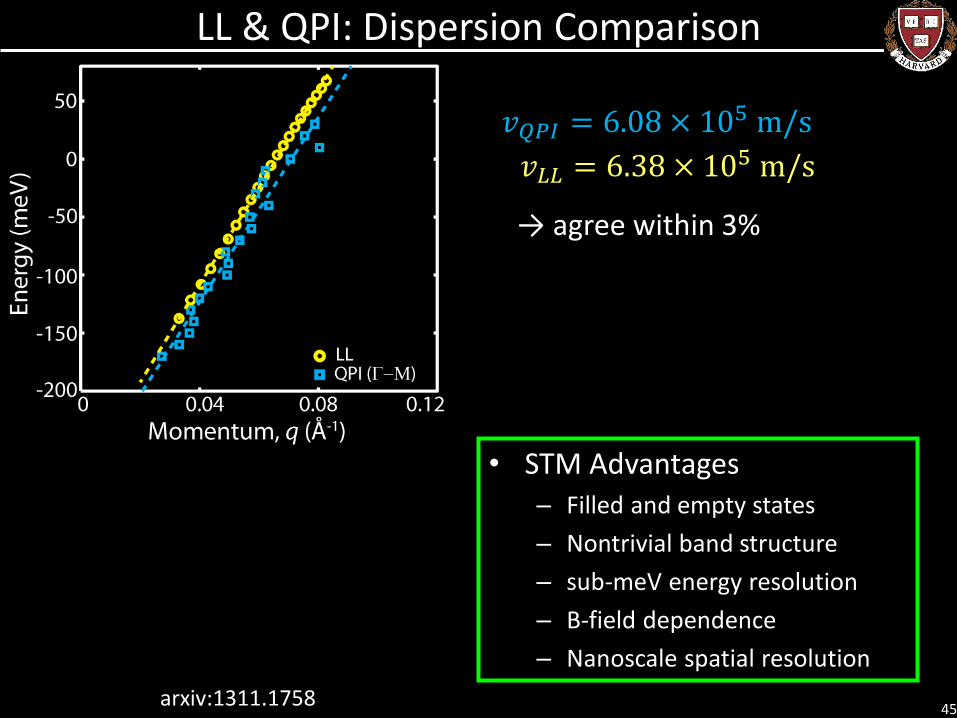
LL & QPI: Dispersion Comparison
45
→ agree within 3%
𝑣𝑄𝑃𝐼 = 6.08 × 10⁵ m/s
𝑣𝐿𝐿 = 6.38 × 10⁵ m/s
• STM Advantages – Filled and empty states
– Nontrivial band structure
– sub-meV energy resolution
– B-field dependence
– Nanoscale spatial resolution
arxiv:1311.1758

Outline
46
• Topological Insulators
• Scanning Tunneling Microscopy
• Nanoscale Band Structure • Topological: Sb
• Insulator: SmB6

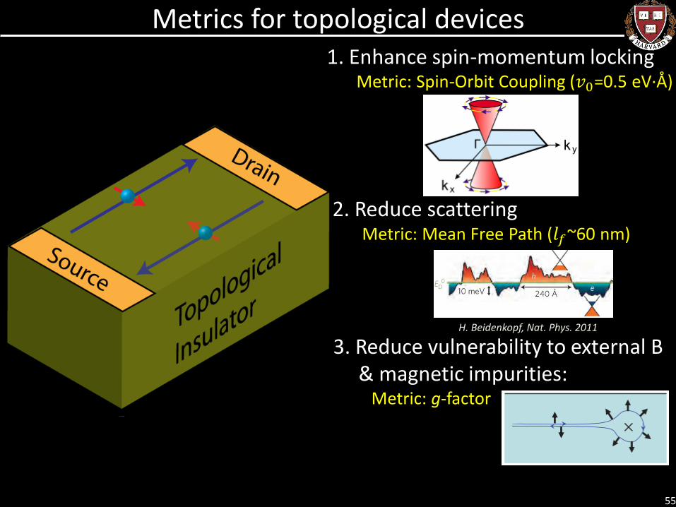
Metrics for topological devices
47
1. Enhance spin-momentum locking Metric: Spin-Orbit Coupling (𝑣0)
3. Reduce vulnerability to external B & magnetic impurities:
Metric: g-factor
H. Beidenkopf, Nat. Phys. 2011
2. Reduce scattering Metric: Mean Free Path (𝑙𝑓)

Reconstruct multi-component band structure
49
LL QPI
Γ 𝑀
𝐾
𝜀𝑆
𝜀𝑇

Reconstruct multi-component band structure
50
LL QPI
Γ 𝑀
𝐾
𝜀𝑆
𝜀𝑇
𝜀 > 𝜀𝑆

Reconstruct multi-component band structure
𝐻 = 𝐸𝐷 +𝑘2
2𝑚∗ + (𝑣0 + 𝛼𝑘2)(𝑘𝑥𝜎𝑦 − 𝑘𝑦𝜎𝑥) +1
2𝜆(𝑘+
3 + 𝑘−3 )
𝐸𝐷 = −210 mV; 𝑚∗ = 0.1𝑚𝑒; 𝑣0 = 0.51 eV⋅Å;
𝛼 = 110eV⋅Å3; 𝜆 = 230 eV⋅Å3
51
LL QPI
𝜀𝑆
𝜀𝑇
𝜀 > 𝜀𝑆

Metrics for topological devices
52
1. Enhance spin-momentum locking Metric: Spin-Orbit Coupling (𝑣0=0.5 eV·Å)
3. Reduce vulnerability to external B & magnetic impurities:
Metric: g-factor
H. Beidenkopf, Nat. Phys. 2011
2. Reduce scattering Metric: Mean Free Path (𝑙𝑓)

LL ‘Sharpness’ & Lifetime Broadening
53
• LLs are sharpest at 𝜀𝐹
in agreement with Fermi liquid theory:
𝜏𝑒−𝑒(𝜀)~1/𝜀2
• Sb(111) mean free path
ℓ ~ℏ
Γ(𝜀𝐹)⋅ 𝑣𝐹
Sample 1: 𝜆𝐹 ~ 65 nm Sample 2: 𝜆𝐹 ~ 59 nm (same for 7.5T & 9T)
Sb(111)

LL ‘Sharpness’ & Lifetime Broadening
54
• LLs are sharpest at 𝜀𝐹
in agreement with Fermi liquid theory:
𝜏𝑒−𝑒(𝜀)~1/𝜀2
• Sb(111) mean free path
ℓ ~ℏ
Γ(𝜀𝐹)⋅ 𝑣𝐹
Sample 1: 𝜆𝐹 ~ 65 nm Sample 2: 𝜆𝐹 ~ 59 nm (same for 7.5T & 9T)
Sb(111)
H. Beidenkopf, Nat. Phys. 2011
c.f. Bi2Se3 Bi2Te3
24 nm
Comparable to distance between strong surface defects
Metrics for topological devices
55
1. Enhance spin-momentum locking Metric: Spin-Orbit Coupling (𝑣0=0.5 eV·Å)
3. Reduce vulnerability to external B & magnetic impurities:
Metric: g-factor
H. Beidenkopf, Nat. Phys. 2011
2. Reduce scattering Metric: Mean Free Path (𝑙𝑓~60 nm)

Quantify g-factor from low-energy LLs
Rashba: 2 split parabolas
𝜀0 = 12
ℏ𝜔𝑐 + 𝑔𝜇𝐵𝐵
𝜀𝑛± = ℏ𝜔𝑐𝑛 ± 2𝑛𝑣0
2𝑚ℏ𝜔𝑐 + 𝜀02
(where 𝜔𝑐 = 𝑒𝐵
𝑚𝑐)
𝜀
𝑘
57
LL QPI
Dirac Fermions: 𝜀 = ℏ𝑣𝐹𝑘
𝜀𝑁 = 𝜀𝐷 + 𝑒ℏ𝑣𝐹𝑁𝐵
𝜀
𝑘
𝜀1
𝜀2 𝜀3
Need to look at low N to get the 𝑔-factor…
𝜀𝑆
𝜀𝑇

Landau level identification in Sb(111)
58
n=0 n=1+
n=2+
n=3+
𝜀0 = 12
ℏ𝜔𝑐 + 𝑔𝜇𝐵𝐵
→ 𝑔 = 12.8

Metrics for topological devices
59
1. Enhance spin-momentum locking Metric: Spin-Orbit Coupling (𝑣0=0.5 eV·Å)
3. Reduce vulnerability to external B & magnetic impurities:
Metric: g-factor (𝑔 = 12.8)
H. Beidenkopf, Nat. Phys. 2011
2. Reduce scattering Metric: Mean Free Path (𝑙𝑓~60 nm)

Robust Surface States in Semimetal Sb
60
Material (Group) LL Range (N) Bulk Overlap (N)
Bi2Se3 (RIKEN) PRB 82, 081305 (2010)
0 : 22 (9 T) ~ 18 (VB)
Sb2Te3 (MBE, CAS) PRL 108, 016401 (2012)
-4 : 8 (7 T) ~ -3 (VB), ~6 (CB)
Bi2Te3 (BC) PRL 109, 166407 (2012)
~ 0 : 14 (7 T) ~ N = 0-15
Pb1-xSnxSe (BC) Science 341, 1496 (2013)
-2 :18 (3-7.5T) ~ N = 7-18
Bi2Te2Se (RIKEN) ACS Nano 7, 4105 (2013)
~ 0 : 17 (11 T) ~ N = 0
Sb (Harvard) 1 : 27 (4 – 9 T) Full
LL
Sb(111)
→ suggests to shift focus from topological insulators to topological semimetals 𝜀𝑆
𝜀𝑇

Topological Semimetal vs. Insulator
61
Sb: bulk semimetal Flat topography, electronic modulations primarily around impurities
100 mV, 1 GΩ
Bi0.92Sb0.08: bulk insulator Large chemical potential fluctuations
Roushan, Nature 460, 1106 (2009)

Sb vs. “canonical” Bi2Se3
Bi2Se3 Sb
Zhu, … Elfimov, Damascelli, PRL 107, 186405 (2011) Zhu, … Elfimov, Damascelli, PRL 110, 216401 (2013)
→ Sb is an excellent platform for exploring topological proximity effects
𝜀𝑆
𝜀𝑇
62

Outline
65
• Topological Insulators
• Scanning Tunneling Microscopy
• Nanoscale Band Structure • Topological: Sb
• Insulator: SmB6

Topological Kondo Insulator
Tk Tk 0K High T
conduction band
f band
Hybridization gap, Δ
f band hybridization
66
Kondo metal Kondo insulator
Topological Kondo Insulator
Tk Tk 0K High T
conduction band
f band
Hybridization gap, Δ
𝐸𝐹
topological surface states
topological Kondo insulator
67

SmB6 as possible TKI
Resistivity
LDA
Lu, PRL 110, 096401 (2013)
68
Zhang, PRX 3, 011011 (2013)
Kondo insulator transition?
resistance saturates
Wolgast, PRB 88, 180405 (2013)

Hybridization gap in SmB6 Transport: Δ = 4.6 meV …… Menth, PRL 22, 295 (1969)
Δ = 11.2 meV ……Flachbart, PRB 64, 085104 (2001)
Δ = 3.47 meV ……Wolgast, PRB 88, 180405 (2013)
Reflectivity & transmissivity: Δ = 4.7 meV ……Travaglini, PRB 29, 893 (1984)
Δ = 19 meV ……Gorshunov, PRB 59, 1808 (1999)
Raman spectroscopy: Δ = 36 meV ……Nyhus, PRB 52, R14308 (1995)
Planar tunneling / point contact spectroscopy: Δ = 2.7 meV ……Güntherodt, PRL 49, 1030 (1982)
Δ = 14 meV ……Amsler, PRB 57, 8747 (1998)
Δ = 22 meV ……Flachbart ,PRB 64, 085104 (2001)
Δ = 18 meV ……Zhang, PRX 3, 011011 (2013)
ARPES: (seven contradictory papers in last few months!) Δ ranges from < 5 meV (entirely below 𝐸𝐹) to > 20 meV (spanning 𝐸𝐹)
69

SmB6 ARPES
Miyazaki, PRB 86, 075105 (2012) Xu, PRB 88, 121102 (2013)
Jiang, Nat Comm 4, 3010 (2013) Neupane, Nat Comm 4, 2991 (2013)
Frantzeskakis, PRX 3, 041024 (2013)
But where is the hybridization gap??
Zhu + Damascelli, PRL 111, 216402 (2013)
Suga, JPSJ 83, 014705 (2014)
70

SmB6 ARPES
6H7/2 (meV)
6H5/2 (meV)
𝚫 (meV)
Spans 𝑬𝑭?
In-gap state? Reference
-200 -15 (X) to -20 (Γ)
~ 15 YES -4 to -8 meV, weakly dispersing
Miyazaki, PRB 86, 075105 (2012)
-160 -20 ~ 20 YES 2 dispersing bands Xu (H. Ding), PRB 88, 121102 (2013)
-150 -18 > 18 YES 2 dispersing bands, circular dichroism
Jiang (D.L. Feng), Nat Com 4, 3010 (2013)
-150 -15 14 NO -4 meV, non-dispersing
Neupane (Z. Hasan), Nat Com 4, 2991 (2013)
-170 -40 < 5 meV NO cannot resolve Frantzeskakis (M. Golden),
PRX 3, 041024 (2013)
-150 -20 ∼ 𝐸𝐹 , ∼ −2 eV dispersing
Zhu (A. Damascelli), PRL 111, 216402 (2013)
-150 -18 Suga, JPSJ 83, 014705 (2014)
SmB6 is not even a Kondo insulator !?!?!
→ Need reliable, spatially resolved, empty + filled state measure of Δ
f band energies
71

SmB6 single crystal
• grown by Al flux method • cleaved in cryogenic UHV • exposes (001) plane • surface B:Sm ratio > 6:1
→ insert into STM
4.13 Å
72

SmB6 atomic surface morphologies
Sm 1 x 1 Sm 2 x 1 B filamentary disordered
c.f. ARPES: 6H7/2 ~ -160 to -150 6H5/2 ~ -20 to -14 → band bending at this polar 1 x 1 surface
73
-28 -165 -8 -155

1x1 surfaces: Polarity-driven surface states?
4.13 Å
Zhu & Damascelli, PRL 111, 216402 (2013) 74

2x1 non-polar: SmB6 hybridization gap?
Can we just read Δ off from the spectrum?
Δ ≈ 20 mV ??
Not so fast… 75

Tunneling into Kondo impurity: Fano resonance
STM tip
tunneling into conduction band
tunneling into Co d orbital
Madhavan, Science 280, 567 (1998)
Co on Au(111)
𝑑𝐼
𝑑𝑉V ∝
𝑞 + 𝜖 2
1 + 𝜖2
Interference between two tunneling channels gives Fano resonance: 𝑞 = ratio between tunneling channels 𝜖 = (eV − 𝜖0)/𝑤 ; 𝜖0 = bare resonance; 𝑤 = resonance width
Not a gap: energy range of destructive interference
76

Tunneling into a Kondo Lattice
Maltseva, Dzero & Coleman, PRL 103, 206402 (2009)
Figgins & Morr, PRL 104, 187202 (2010)
Dirty Kondo lattice: Fano is the limiting case
Clean Kondo lattice: analytic model, structureless conduction band
Clean Kondo lattice: computational model, realistic conduction band
Yang, PRB 79, 241107 (2009) Wolfle, Dubi & Balatsky, PRL 105, 246401 (2010)
77

SmB6 bands from ARPES ARPES filled states
Jiang, Nat Comm 4, 3010 (2013)
LDA for empty states
Antonov, PRB 66, 165209 (2002)
our model
Sm 5d conduction band −𝐷1= −1.6 eV ; 𝐷2 = 3 eV
78

Figgins vs. Maltseva Models
Maltseva Figgins Raw data
Both models: 𝛾 = 𝑘𝐵𝑇 (𝑇 = 8 K)
𝑡𝑓
𝑡𝑐= −0.055
⇒ 𝑣 ~155 meV in both models
Raw dI/dV data
79
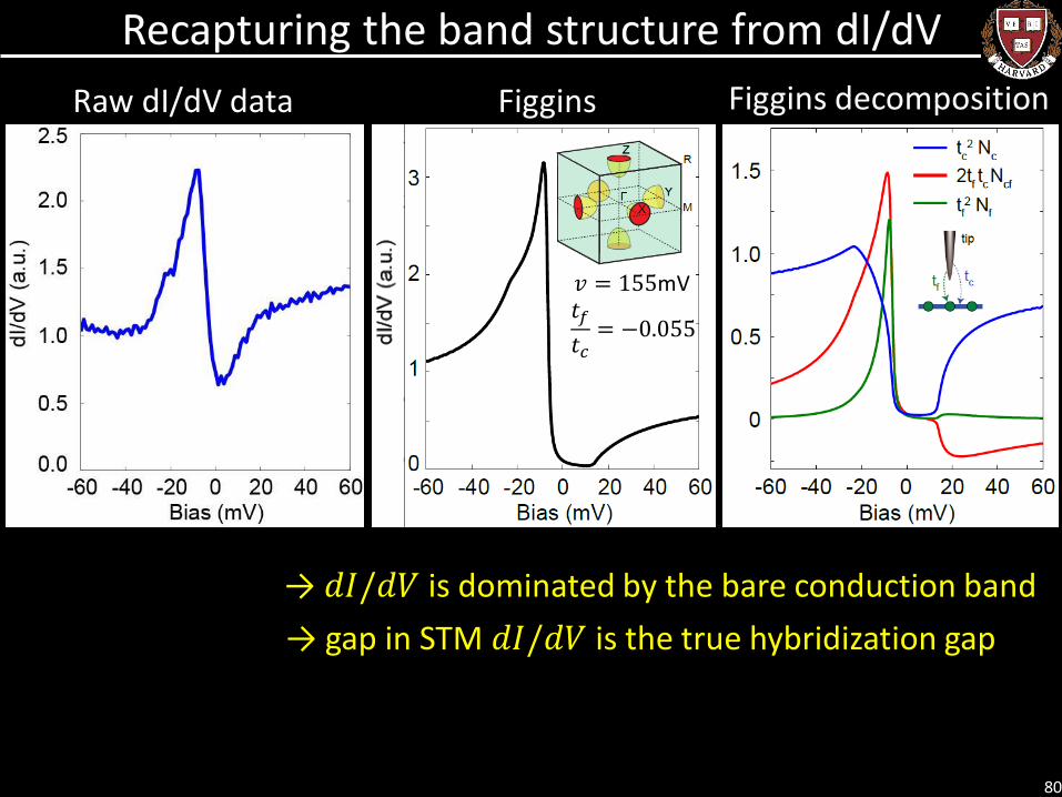
Recapturing the band structure from dI/dV
Figgins Figgins decomposition
→ 𝑑𝐼/𝑑𝑉 is dominated by the bare conduction band
→ gap in STM 𝑑𝐼/𝑑𝑉 is the true hybridization gap
Raw dI/dV data
80
Δ ∼2𝑣2
𝐷∼ 13 𝑚𝑒𝑉
𝑣 = 155mV 𝑡𝑓
𝑡𝑐= −0.055
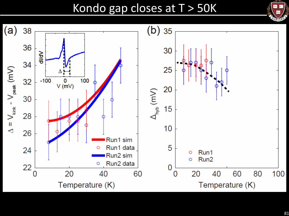
Kondo gap closes at T > 50K
81

Comparison to “Point Contact Spectroscopy”
STM (vacuum tunneling)
Amsler, PRB 57, 8747 (1998)
Zhang, PRX 3, 011011 (2013)
Ag contact, ~ 100 mm
Pb contact, unknown size
→ prominent peak is on opposite side
Planar tunneling
82

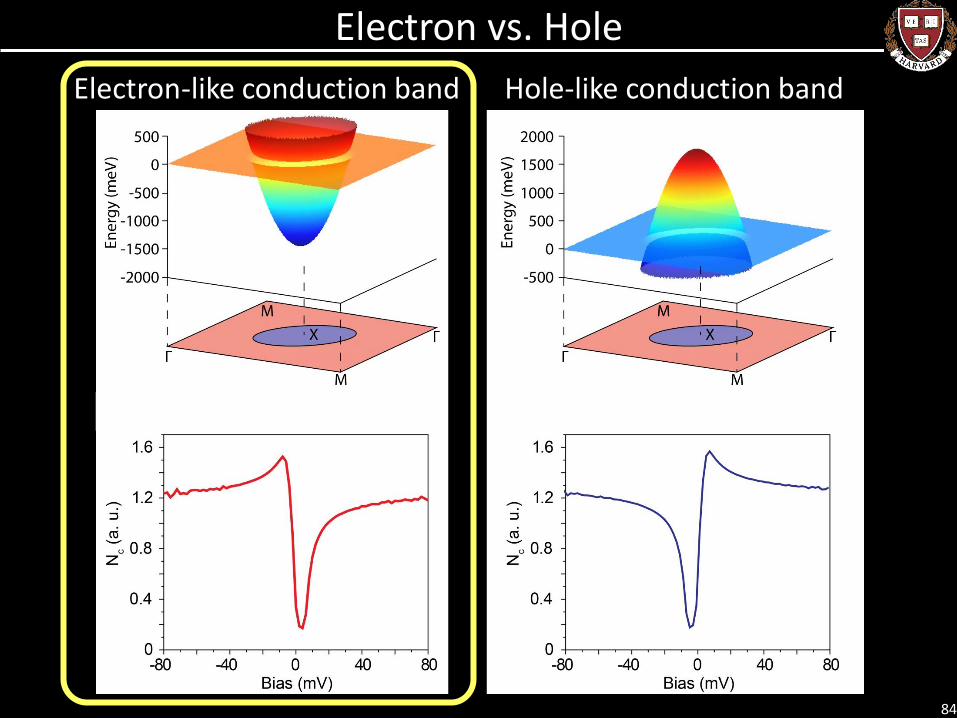
Electron vs. hole
Hole-like conduction
band
Electron-like conduction
band
→ Expect conduction band peak on negative side
83
In 3-dim, “outside shell” will give more prominent peak than “inside shell”
Electron vs. Hole
Hole-like conduction band Electron-like conduction band
84
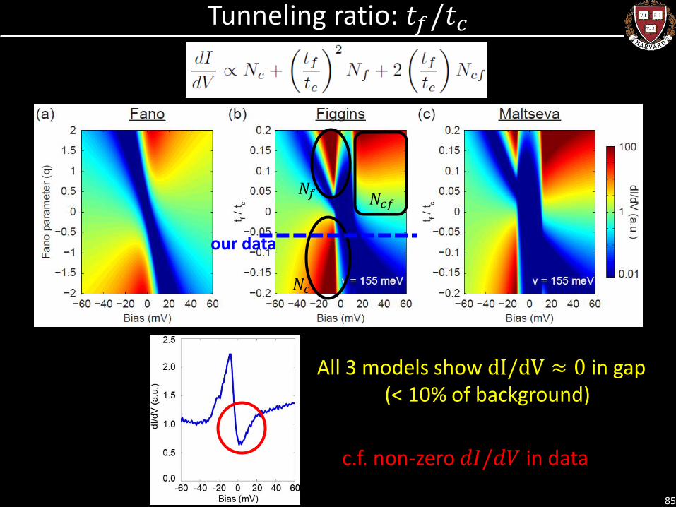
Tunneling ratio: 𝑡𝑓/𝑡𝑐
𝑁𝑐
𝑁𝑓 𝑁𝑐𝑓
our data
All 3 models show dI/dV ≈ 0 in gap (< 10% of background)
c.f. non-zero 𝑑𝐼/𝑑𝑉 in data
85

Comparison to ARPES 6H7/2
(meV)
6H5/2 (meV)
𝚫 (meV)
Spans 𝑬𝑭?
In-gap state? 2x1 ? Reference
-200 -15 (X) to -20 (Γ)
~ 15 YES -4 to -8 meV, weakly dispersing
yes (LEED)
Miyazaki, PRB 86, 075105 (2012)
-160 -20 ~ 20 YES 2 dispersing bands yes (folding)
Xu (H. Ding), PRB 88, 121102 (2013)
-150 -18 > 18 YES 2 dispersing bands, circular dichroism
yes (folding)
Jiang (D.L. Feng), Nat Com 4, 3010 (2013)
-150 -15 14 NO -4 meV, non-dispersing
? Neupane (Z. Hasan), Nat Com 4, 2991 (2013)
-170 -40 < 5
meV NO cannot resolve no (LEED)
Frantzeskakis (Golden), PRX 3, 041024 (2013)
-150 -20 ∼ 𝐸𝐹, ∼ −2 eV dispersing
no (LEED)
Zhu (Damascelli), PRL 111, 216402 (2013)
-150 -18 ? Suga,
JPSJ 83, 014705 (2014)
→ partial 2x1 surface gives the -8 meV state: this is the f band itself, not an “in-gap” state!! f band energies
→ complete 1x1 surface causes band-bending, looks like Kondo metal? 86

-28 -165 -8 -155
SmB6 conclusions
1. Band bending on varying surface morphologies
Sm 1 x 1 Sm 2 x 1
3. Residual ‘in-gap’ spectral weight
Next step: QPI to look for Dirac cone
87 arxiv:1308.1085
2. Hybridization gap spans 𝐸𝐹 → Kondo insulator
Need to decompose dI/dV into DOS & interference

Conclusions
88
• Nanoscale Band Structure o Quasiparticle Interference
o Landau Quantization
→ Reconciled!!
• Topological surface states in Sb: o mean free path → ℓ = 65 nm
o spin-orbit coupling → 𝑣0 = 0.51 eV⋅Å
o g-factor → 𝑔 = 12.8
• SmB6: Topological Kondo Insulator? o Hybridization gap spans 𝐸𝐹 → Kondo insulator
o In-gap spectral weight → topological surface state?
arxiv:1308.1085
arxiv:1311.1758