hx6256 32k x 8 static ram - honeywell · hx6256 32k x 8 static ram . ... threshold shift...
TRANSCRIPT

HX6256 32K x 8 Static RAM
The 32K x 8 Radiation Hardened Static RAM is a high performance 32,768
word x 8-bit static random access memory with industry-standard
functionality. It is fabricated with Honeywell’s radiation hardened
technology, and is designed for use in systems operating in radiation
environments. The RAM operates over the full military temperature range
and requires only a single 5 V ± 10% power supply. The RAM is available
with either TTL or CMOS compatible I/O. Power consumption is typically
less than 15 mW/MHz in operation, and less than 5 mW when de-selected.
The RAM read operation is fully asynchronous, with an associated typical
access time of 17 ns at 5 V.
Honeywell’s enhanced SOI RICMOS™ IV (Radiation Insensitive CMOS)
technology is radiation hardened through the use of advanced and
proprietary design, layout, and process hardening techniques. The
RICMOS™ IV process is a 5-volt, SOI CMOS technology with a 150 Å gate oxide and a minimum drawn feature size of
0.7 µm (0.6 µm effective gate length—Leff). Additional features include tungsten via plugs, Honeywell’s proprietary SHARP
planarization process, and a lightly doped drain (LDD) structure for improved short channel reliability. A 7 transistor (7T)
memory cell is used for superior single event upset hardening, while three layer metal power bussing and the low
collection volume SOI substrate provide improved dose rate hardening.
FEATURES
RADIATION • Fabricated with RICMOS™ IV Silicon on Insulator
(SOI) 0.7 µm Process (Leff = 0.6 µm) • Total Dose Hardness through 1x10⁶
rad(SiO2) • Neutron Hardness through 1x1014 cm-2 • Dynamic and Static Transient Upset Hardness
through 1x10⁹ rad(Si)/s • Dose Rate Survivability through 1x10¹¹ rad(Si)/s • Soft Error Rate of <1x10⁻¹⁰ upsets/bit-day in
Geosynchronous Orbit • Immune from Latchup
OTHER • Listed On SMD#5962–95845 • Fast Cycle Times
o ≤ 17 ns (Typical) o ≤ 25 ns (-55 to 125°C) Read Write Cycle
• Asynchronous Operation
o CMOS or TTL Compatible I/O • Single 5 V ± 10% Power Supply • Packaging Options
o 28-Lead CFP (0.500 in. x 0.720 in.) o 28-Lead DIP, MIL-STD-1835, CDIP2-T28 o 36-Lead CFP—Bottom Braze (0.630 x 0.650 in.) o 36-Lead CFP—Top Braze (0.630 x 0.650 in.)
HX6256
2 www.honeywellmicroelectronics.com
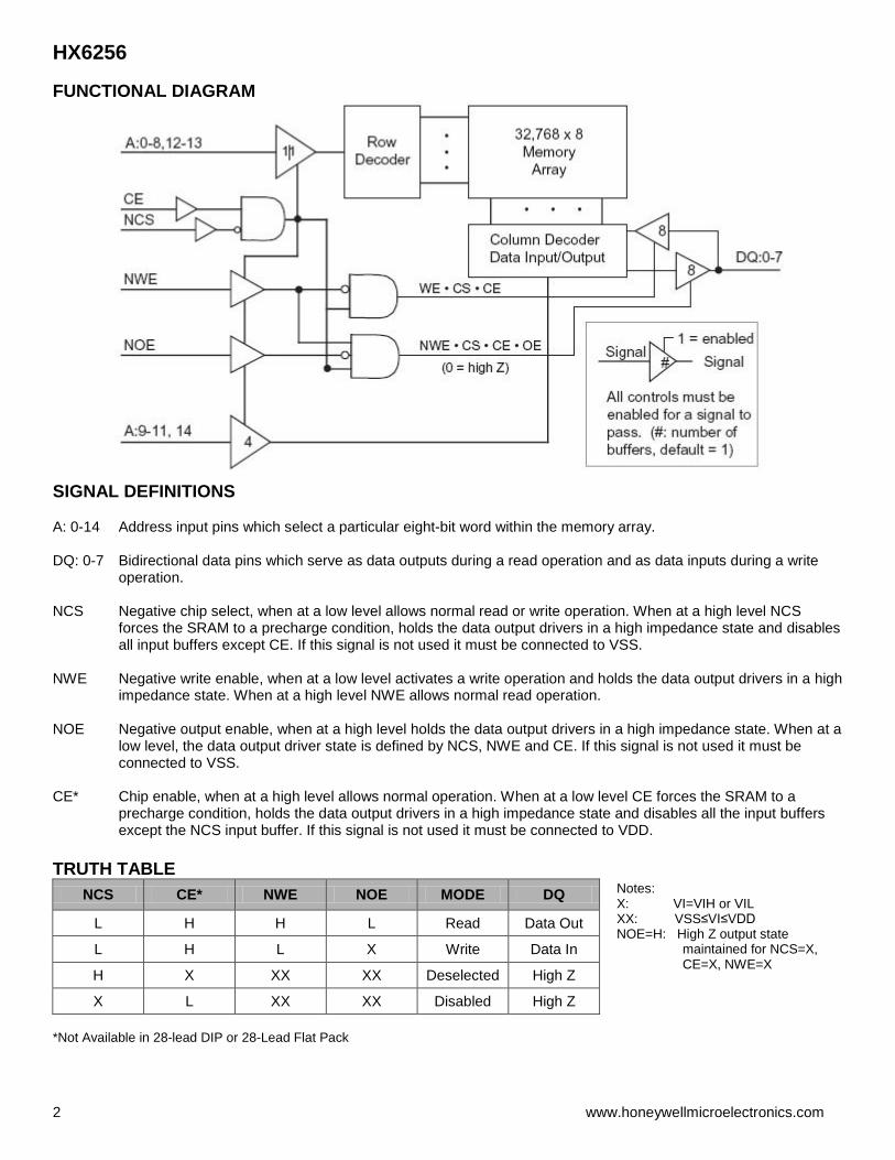
FUNCTIONAL DIAGRAM
SIGNAL DEFINITIONS A: 0-14 Address input pins which select a particular eight-bit word within the memory array. DQ: 0-7 Bidirectional data pins which serve as data outputs during a read operation and as data inputs during a write
operation. NCS Negative chip select, when at a low level allows normal read or write operation. When at a high level NCS
forces the SRAM to a precharge condition, holds the data output drivers in a high impedance state and disables all input buffers except CE. If this signal is not used it must be connected to VSS.
NWE Negative write enable, when at a low level activates a write operation and holds the data output drivers in a high
impedance state. When at a high level NWE allows normal read operation. NOE Negative output enable, when at a high level holds the data output drivers in a high impedance state. When at a
low level, the data output driver state is defined by NCS, NWE and CE. If this signal is not used it must be connected to VSS.
CE* Chip enable, when at a high level allows normal operation. When at a low level CE forces the SRAM to a
precharge condition, holds the data output drivers in a high impedance state and disables all the input buffers except the NCS input buffer. If this signal is not used it must be connected to VDD.
TRUTH TABLE
NCS CE* NWE NOE MODE DQ
L H H L Read Data Out
L H L X Write Data In
H X XX XX Deselected High Z
X L XX XX Disabled High Z *Not Available in 28-lead DIP or 28-Lead Flat Pack
Notes: X: VI=VIH or VIL XX: VSS≤VI≤VDD NOE=H: High Z output state
maintained for NCS=X, CE=X, NWE=X

HX6256
www.honeywellmicroelectronics.com 3
RADIATION CHARACTERISTICS Total Ionizing Radiation Dose The SRAM will meet all stated functional and electrical specifications over the entire operating temperature range after the specified total ionizing radiation dose. All electrical and timing performance parameters will remain within specifications after rebound at VDD = 5.5 V and T =125°C extrapolated to ten years of operation. Total dose hardness is assured by wafer level testing of process monitor transistors and RAM product using 10 KeV X-ray and Co60 radiation sources. Transistor gate threshold shift correlations have been made between 10 KeV X-rays applied at a dose rate of 1x10⁵
rad(SiO2)/min at T = 25°C and gamma rays (Cobalt 60 source) to ensure that wafer level X-ray testing is consistent with standard military radiation test environments. Transient Pulse Ionizing Radiation The SRAM is capable of writing, reading, and retaining stored data during and after exposure to a transient ionizing radiation pulse up to the transient dose rate upset specification, when applied under recommended operating conditions. To ensure validity of all specified performance parameters before, during, and after radiation (timing degradation during transient pulse radiation is ≤10%), it is suggested that stiffening capacitance be placed on or near the package VDD and VSS, with a maximum inductance between the package (chip) and stiffening capacitance of 0.7 nH per part. If there are no operate-through or valid stored data requirements, typical circuit board mounted de-coupling capacitors are recommended.
The SRAM will meet any functional or electrical specification after exposure to a radiation pulse up to the transient dose rate survivability specification, when applied under recommended operating conditions. Note that the current conducted during the pulse by the RAM inputs, outputs, and power supply may significantly exceed the normal operating levels. The application design must accommodate these effects. Neutron Radiation The SRAM will meet any functional or timing specification after exposure to the specified neutron fluence under recommended operating or storage conditions. This assumes equivalent neutron energy of 1 MeV. Soft Error Rate The SRAM is immune to Single Event Upsets (SEU’s) to the specified Soft Error Rate (SER), under recommended operating conditions. This hardness level is defined by the Adams 90% worst case cosmic ray environment for geosynchronous orbits. Latchup The SRAM will not latch up due to any of the above radiation exposure conditions when applied under recommended operating conditions. Fabrication with the SOI substrate material provides oxide isolation between adjacent PMOS and NMOS transistors and eliminates any potential SCR latchup structures. Sufficient transistor body tie connections to the p- and n-channel substrates are made to ensure no source/drain snapback occurs.
RADIATION HARDNESS RATINGS (1)
Parameter Limits (2) Units Test Conditions
Total Dose ≥1x10⁶ rad(Si) TA=25°C
Transient Dose Rate Upset (3) ≥1x10⁹ rad(Si)/s Pulse width ≤ 50ns
Transient Dose Rate Survivability (3) ≥1x10¹¹ rad(Si)/s Pulse width ≤50 ns, X-ray, VDD=6.0V, TA=25°C
Soft Error Rate (SER) <1x10⁻¹⁰ upsets/bit-day TA=25°C, Adams 90% worst case environment
Neutron Fluence ≥1x10¹⁴ N/cm2 1 MeV equivalent energy, Unbiased, TA=25°C (1) Device will not latch up due to any of the specified radiation exposure conditions. (2) Operating conditions (unless otherwise specified): VDD=4.5 V to 5.5 V, TA=-55°C to 125°C. (3) Not guaranteed with 28–Lead DIP.

HX6256
4 www.honeywellmicroelectronics.com
ABSOLUTE MAXIMUM RATINGS (1)
Symbol Parameter Rating
Units Min Max VDD Supply Voltage Range (2) -0.5 7.0 V VPIN Voltage on Any Pin (2) -0.5 VDD +0.5 V TSTORE Storage Temperature (Zero Bias) -65 150 °C TSOLDER Soldering Temperature (5 Seconds) 270 °C PD Maximum Power Dissipation (3) 2.5 W IOUT DC or Average Output Current 25 mA VPROT ESD Input Protection Voltage (4) 2000 V
ΘJC Thermal Resistance (Jct-toCase) 28 FP/36 FP 2
°C/W 28 DIP 10
TJ Junction Temperature 175 °C (1) Stresses in excess of those listed above may result in permanent damage. These are stress ratings only, and operation at these
levels is not implied. Frequent or extended exposure to absolute maximum conditions may affect device reliability. (2) Voltage referenced to VSS. (3) RAM power dissipation (IDDSB + IDDOP) plus RAM output driver power dissipation due to external loading must not exceed this
specification. (4) Class 2 electrostatic discharge (ESD) input protection. Tested per MIL-STD-883, Method 3015 by DESC certified lab. RECOMMENDED OPERATING CONDITIONS
Symbol Parameter Description
Units Min Typ Max VDD Supply Voltage (referenced to VSS) 4.5 5.0 5.5 V TA Ambient Temperature -55 25 125 °C VPIN Voltage on Any Pin (referenced to VSS) -0.3 VDD+0.3 V VDDRAMP VDD Turn on ramp time 50 ms
CAPACITANCE (1)
Symbol Parameter Typical (1) Worst Case
Units Test Conditions Min Max CI Input Capacitance 5 7 pF VI=VDD or VSS, f=1 MHz CO Output Capacitance 7 9 pF VIO=VDD or VSS, f=1 MHz
(1) This parameter is tested during initial design characterization only. DATA RETENTION CHARACTERISTICS
Symbol Parameter Typical (1) Worst Case (2)
Units Test Conditions Min Max
VDR Data Retention Voltage 2.5 V NCS=VDR VI=VDR or VSS
IDR Data Retention Current 500 μA NCS=VDD=2.5V, VI=VDD or VSS
(1) Typical operating conditions: TA= 25°C, pre-radiation. (2) Worst case operating conditions: TA= -55°C to +125°C, post total dose at 25°C.

HX6256
www.honeywellmicroelectronics.com 5
DC ELECTRICAL CHARACTERISTICS
Symbol Parameter Worst Case (2)
Units Test Conditions Min Max
IDDSB1 Static Supply Current 1.5 mA VIH=VDD, IO=0 VIL=VSS, f=0MHz
IDDSBMF Standby Supply Current – Deselected 1.5 mA NCS=VDD, IO=0,
f=40 MHZ
IDDOPW
Dynamic Supply Current – Selected (Write) 1MHz 2MHz 10MHz 25MHz 40MHz
4 8 40 100 160
mA IO=0, CE=VIH=VDD NCS=VIL=VSS (3)
IDDOPR
Dynamic Supply Current – Selected (Read) 1MHz 2MHz 10MHz 25MHz 40MHz
4 8 40 100 160
mA IO=0, CE=VIH=VDD NCS=VIL=VSS (3)
II Input Leakage Current -5 +5 μA VSS ≤ VI ≤ VDD
IOZ Output Leakage Current -10 +10 μA VSS ≤ VI ≤ VDD Output = high Z
VIL Low-Level Input Voltage CMOS TTL 0.3xVDD
0.8 V March Pattern
VIH High-Level Input Voltage CMOS TTL
0.7xVDD 2.2 V March Pattern
VOL Low-Level Output Voltage 0.4 0.05 V
VDD=4.5V, IOL = 10 mA (CMOS),= 8 mA (TTL) VDD=4.5V, IOL = 200 μA
VOH High-Level Output Voltage 4.2 VDD-0.05 V VDD=4.5V, IOH=-5mA
VDD=4.5V, IOH=-200 μA (1) Not applicable (2) Worst case operating conditions: VDD=4.5 V to 5.5 V, TA=-55°C to +125°C, post total dose at 25°C. (3) All inputs switching. DC average current. TESTER EQUIVALENT LOAD CIRCUIT
HX6256
6 www.honeywellmicroelectronics.com
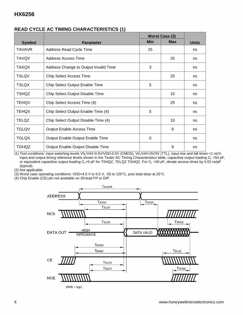
READ CYCLE AC TIMING CHARACTERISTICS (1)
Symbol Parameter Worst Case (3)
Units Min Max
TAVAVR Address Read Cycle Time 25 ns
TAVQV Address Access Time 25 ns
TAXQX Address Change to Output Invalid Time 3 ns
TSLQV Chip Select Access Time 25 ns
TSLQX Chip Select Output Enable Time 5 ns
TSHQZ Chip Select Output Disable Time 10 ns
TEHQV Chip Select Access Time (4) 25 ns
TEHQX Chip Select Output Enable Time (4) 5 ns
TELQZ Chip Select Output Disable Time (4) 10 ns
TGLQV Output Enable Access Time 9 ns
TGLQX Output Enable Output Enable Time 0 ns
TGHQZ Output Enable Output Disable Time 9 ns (1) Test conditions: input switching levels VIL/VIH=0.5V/VDD-0.5V (CMOS), VIL/VIH=0V/3V (TTL), input rise and fall times <1 ns/V,
input and output timing reference levels shown in the Tester AC Timing Characteristics table, capacitive output loading CL >50 pF, or equivalent capacitive output loading CL=5 pF for TSHQZ, TELQZ TGHQZ. For CL >50 pF, derate access times by 0.02 ns/pF (typical).
(2) Not applicable. (3) Worst case operating conditions: VDD=4.5 V to 5.5 V, -55 to 125°C, post total dose at 25°C. (4) Chip Enable (CE) pin not available on 28-lead FP or DIP.

HX6256
www.honeywellmicroelectronics.com 7
WRITE CYCLE AC TIMING CHARACTERISTICS (1)
Symbol Parameter Worst Case (3)
Units Min Max TAVAVW Write Cycle Time 25 ns
TWLWH Write Enable Write Pulse Width 20 ns
TSLWH Chip Select to End of Write Time 20 ns
TDVWH Data Valid to End of Write Time 15 ns
TAVWH Address Valid to End of Write Time 20 ns
TWHDX Data Hold Time after End of Write Time 0 ns
TAVWL Address Valid Setup to Start of Write Time 0 ns
TWHAX Address Valid Hold after End of Write Time 0 ns
TWLQZ Write Enable to Output Disable Time 0 9 ns
TWHQX Write Disable to Output Enable Time 5 ns
TWHWL Write Disable to Write Enable Pulse Width (5) 5 ns
TEHWH Chip Enable to End of Write Time (6) 20 ns (1) Test conditions: input switching levels VIL/VIH=0.5V/VDD-0.5V (CMOS), VIL/VIH=0V/3V (TTL), input rise and fall times <1 ns/V,
input and output timing reference levels shown in the Tester AC Timing Characteristics table, capacitive output loading >50 pF, or equivalent capacitive load of 5 pF for TWLQZ.
(2) Typical operating conditions: VDD=5.0 V, TA=25°C, pre-radiation. (3) Worst case operating conditions: VDD=4.5 V to 5.5 V, -55 to 125°C, post total dose at 25°C. (4) TAVAV = TWLWH + TWHWL (5) Guaranteed but not tested. (6) Chip Enable (CE) pin not available on 28-lead FP or DIP.

HX6256
8 www.honeywellmicroelectronics.com
DYNAMIC ELECTRICAL CHARACTERISTICS Read Cycle The RAM is asynchronous in operation, allowing the read cycle to be controlled by address, chip select (NCS), or chip enable (CE) (refer to Read Cycle timing diagram). To perform a valid read operation, both chip select and output enable (NOE) must be low and chip enable and write enable (NWE) must be high. The output drivers can be controlled independently by the NOE signal. Consecutive read cycles can be executed with NCS held continuously low, and with CE held continuously high, and toggling the addresses. For an address activated read cycle, NCS and CE must be valid prior to or coincident with the activating address edge transition(s). Any amount of toggling or skew between address edge transitions is permissible; however, data outputs will become valid TAVQV time following the latest occurring address edge transition. The minimum address activated read cycle time is TAVAV. When the RAM is operated at the minimum address activated read cycle time, the data outputs will remain valid on the RAM I/O until TAXQX time following the next sequential address transition. To control a read cycle with NCS, all addresses and CE must be valid prior to or coincident with the enabling NCS edge transition. Address or CE edge transitions can occur later than the specified setup times to NCS, however, the valid data access time will be delayed. Any address edge transition, which occurs during the time when NCS is low, will initiate a new read access, and data outputs will not become valid until TAVQV time following the address edge transition. Data outputs will enter a high impedance state TSHQZ time following a disabling NCS edge transition. To control a read cycle with CE, all addresses and NCS must be valid prior to or coincident with the enabling CE edge transition. Address or NCS edge transitions can occur later than the specified setup times to CE; however, the valid data access time will be delayed. Any address edge transition which occurs during the time when CE is high will initiate a new read access, and data outputs will not become valid until TAVQV time following the address edge transition. Data outputs will enter a high impedance state TELQZ time following a disabling CE edge transition.
Write Cycle The write operation is synchronous with respect to the address bits, and control is governed by write enable (NWE), chip select (NCS), or chip enable (CE) edge transitions (refer to Write Cycle timing diagrams). To perform a write operation, both NWE and NCS must be low, and CE must be high. Consecutive write cycles can be performed with NWE or NCS held continuously low, or CE held continuously high. At least one of the control signals must transition to the opposite state between consecutive write operations. The write mode can be controlled via three different control signals: NWE, NCS, and CE. All three modes of control are similar except the NCS and CE controlled modes actually disable the RAM during the write recovery pulse. Both CE and NCS fully disable the RAM decode logic and input buffers for power savings. Only the NWE controlled mode is shown in the table and diagram on the previous page for simplicity. However, each mode of control provides the same write cycle timing characteristics. Thus, some of the parameter names referenced below are not shown in the write cycle table or diagram, but indicate which control pin is in control as it switches high or low. To write data into the RAM, NWE and NCS must be held low and CE must be held high for at least TWLWH/TSLSH/TEHEL time. Any amount of edge skew between the signals can be tolerated, and any one of the control signals can initiate or terminate the write operation. For consecutive write operations, write pulses must be separated by the minimum specified TWHWL/TSHSL/TELEH time. Address inputs must be valid at least TAVWL/TAVSL/TAVEH time before the enabling NWE/NCS/CE edge transition, and must remain valid during the entire write time. A valid data overlap of write pulse width time of TDVWH/TDVSH/TDVEL, and an address valid to end of write time of TAVWH/TAVSH/TAVEL also must be provided for during the write operation. Hold times for address inputs and data inputs with respect to the disabling NWE/NCS/CE edge transition must be a minimum of TWHAX/TSHAX/TELAX time and TWHDX/TSHDX/TELDX time, respectively. The minimum write cycle time is TAVAV.

HX6256
www.honeywellmicroelectronics.com 9
TESTER AC TIMING CHARACTERISTICS
QUALITY AND RADIATION HARDNESS ASSURANCE Honeywell maintains a high level of product integrity through process control, utilizing statistical process control, a complete “Total Quality Assurance System,” a computer data base process performance tracking system, and a radiation- hardness assurance strategy. The radiation hardness assurance strategy starts with a technology that is resistant to the effects of radiation. Radiation hardness is assured on every wafer by irradiating test structures as well as SRAM product, and then monitoring key parameters which are sensitive to ionizing radiation. Conventional MIL-STD-883 TM 5005 Group E testing, which includes total dose exposure with Cobalt 60, may also be performed as required. This Total Quality approach ensures our customers of a reliable product by engineering in reliability, starting with process development and continuing through product qualification and screening. SCREENING LEVELS Honeywell offers several levels of device screening to meet your system needs. “Engineering Devices” are available with limited performance and screening for breadboarding and/or evaluation testing. Hi-Rel Level B and S devices undergo additional screening per the requirements of MILSTD-883. As a QML supplier, Honeywell also offers QML Class Q and V devices per MIL-PRF-38535 and are available per the applicable Standard Microcircuit Drawing (SMD). QML devices offer ease of procurement by eliminating the need to create detailed specifications and offer benefits of improved quality and cost savings through standardization.
RELIABILITY Honeywell understands the stringent reliability requirements for space and defense systems and has extensive experience in reliability testing on programs of this nature. This experience is derived from comprehensive testing of VLSI processes. Reliability attributes of the RICMOS™ process were characterized by testing specially designed irradiated and non-irradiated test structures from which specific failure mechanisms were evaluated. These specific mechanisms included, but were not limited to, hot carriers, electromigration and time dependent dielectric breakdown. This data was then used to make changes to the design models and process to ensure more reliable products. In addition, the reliability of the RICMOS™ process and product in a military environment was monitored by testing irradiated and non-irradiated circuits in accelerated dynamic life test conditions. Packages are qualified for product use after undergoing Groups B & D testing as outlined in MIL-STD-883, TM 5005, Class S. The product is qualified by following a screening and testing flow to meet the customer’s requirements. Quality conformance testing is performed as an option on all production lots to ensure the ongoing reliability of the product.
* Input rise and fall times <1 ns/V
HX6256
10 www.honeywellmicroelectronics.com
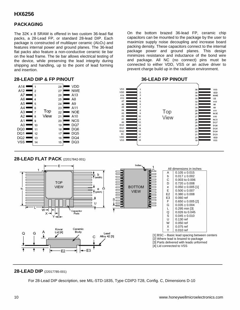
PACKAGING The 32K x 8 SRAM is offered in two custom 36-lead flat packs, a 28-Lead FP, or standard 28-lead DIP. Each package is constructed of multilayer ceramic (Al2O3) and features internal power and ground planes. The 36-lead flat packs also feature a non-conductive ceramic tie bar on the lead frame. The tie bar allows electrical testing of the device, while preserving the lead integrity during shipping and handling, up to the point of lead forming and insertion.
On the bottom brazed 36-lead FP, ceramic chip capacitors can be mounted to the package by the user to maximize supply noise decoupling and increase board packing density. These capacitors connect to the internal package power and ground planes. This design minimizes resistance and inductance of the bond wire and package. All NC (no connect) pins must be connected to either VDD, VSS or an active driver to prevent charge build up in the radiation environment.
28-LEAD DIP & FP PINOUT 36-LEAD FP PINOUT
28-LEAD FLAT PACK (22017842-001)
28-LEAD DIP (22017785-001)
For 28-Lead DIP description, see MIL-STD-1835, Type CDIP2-T28, Config. C, Dimensions D-10
All dimensions in inches A b C D e E E2 E3 F G L Q S U W X Y
0.105 ± 0.015 0.017 ± 0.002 0.003 to 0.006 0.720 ± 0.008 0.050 ± 0.005 [1] 0.500 ± 0.007 0.380 ± 0.008 0.060 ref 0.650 ± 0.005 [2] 0.035 ± 0.004 0.295 min [3] 0.026 to 0.045 0.045 ± 0.010 0.130 ref 0.050 ref 0.075 ref 0.010 ref
[1] BSC – Basic lead spacing between centers [2] Where lead is brazed to package [3] Parts delivered with leads unformed [4] Lid connected to VSS

HX6256
www.honeywellmicroelectronics.com 11
36-LEAD FLAT PACK—BOTTOM BRAZE (22018131-001)
36-LEAD FLAT PACK—TOP BRAZE (22019627-001)
All dimensions in inches A b C D E e F G H I J L
0.095 ± 0.014 0.008 ± 0.002 0.005 to 0.0075 0.650 ± 0.010 0.630 ± 0.007 0.025 ± 0.002 [2] 0.425 ± 0.005 [2] 0.525 ± 0.005 0.135 ± 0.005 0.030 ± 0.005 0.080 typ. 0.285 ± 0.015
M N O P R S T U V W X Y
0.008 ± 0.003 0.050 ± 0.010 0.090 ref 0.015 ref 0.075 ref 0.113 ± 0.010 0.050 ref 0.030 ref 0.080 ref 0.005 ref 0.450 ref 0.400 ref
All dimensions in inches A b C D E e F G H I J L M S
0.085 ± 0.010 0.008 ± 0.002 0.005 to 0.0075 0.650 ± 0.010 0.630 ± 0.007 0.025 ± 0.002 [2] 0.425 ± 0.005 [2] 0.525 ± 0.005 0.135 ± 0.005 0.030 ± 0.005 0.080 typ. 0.285 ± 0.015 0.009 ± 0.003 0.113 ± 0.010
[1] Parts delivered with leads unformed [2] At tie bar [3] Lid tied to VSS
[1] Parts delivered with leads unformed [2] At tie bar [3] Lid tied to VSS

HX6256
12 www.honeywellmicroelectronics.com
DYNAMIC BURN-IN DIAGRAM*
*36-lead Flat Pack burn-in diagram has similar connections and is available on request. ORDERING INFORMATION (1)
Notes: (1) Orders may be faxed to 763-954-2051. (2) For CMOS I/O type only. (3) Engineering Device description: Parameters are tested from -55 to 125°C, 24 hr burn-in, no radiation guaranteed.
The QML Certified SRAM can also be ordered under the SMD drawing 5962–95845. FIND OUT MORE For more information on Honeywell’s SRAM products visit us online at www.honeywell.com/radhard or contact us at 800-323-8295 (763-954-2474 internationally). This product and related technical data is subject to the U.S. Department of State International Traffic in Arms Regulations (ITAR) 22 CFR 120-130 and may not be exported, as defined by the ITAR, without the appropriate prior authorization from the Directorate of Defense Trade Controls, United States Department of State. Diversion contrary to U.S. export laws and regulations is prohibited. The application circuits herein constitute typical usage and interface of Honeywell product. Honeywell does not warranty or assume liability of customer-designed circuits derived from this description or depiction. Honeywell reserves the right to make changes to improve reliability, function or design. Honeywell does not assume any liability arising out of the application or use of any product or circuit described herein; neither does it convey any license under its patent rights nor the rights of others. Honeywell 12001 Highway 55 Plymouth, MN 55441 Tel: 800-323-8295 www.honeywellmicroelectronics.com
Form # ADS-14227 December 2012 ©2012 Honeywell International Inc.
VDD = 5.6V, R ≤ 10 KΩ, VIH = VDD, VIL = VSS Ambient Temperature ≥ 125°C, F0 ≥ 100 KHz Sq Wave
Frequency of F1 = F0/2, F2 = F0/4, F3 = F0/8, etc.
VDD = 5.5V, R ≤ 10 KΩ Ambient Temperature ≥125°C
H X 6256 V H N
SOURCE H = Honeywell
PROCESS X = SOI CMOS
PACKAGE DESIGNATION N = 28 Lead Flatpack
R=28 Lead DIP X=36 Lead FP(bottom braze)(2)
P=36 Lead FP (top braze) - = Bare die
PART NUMBER
SCREEN LEVEL V = QML Class V Q = QML Class Q
S = Class S B = Class B
E = Eng. Model (3)
TOTAL DOSE HARDNESS R = 1x10⁵ rad (Si) F = 3x10⁵ rad (Si) H = 1x10⁶ rad (Si)
N = No Level Guaranteed (3)
C
Input Buffer Type C = CMOS
T = TTL