ibc module - vicor - power supply manufacturer | high ... · pdf fileibc module rev 1.1 page 1...
TRANSCRIPT

IBC Module Rev 1.1 vicorpower.comPage 1 of 17 09/2016 800 927.9474
4:1 Intermediate Bus Converter Module: Up to 500W Output
IBC ModuleIB0xE120T40xx-xx
C US® S
NRTLC US
Size:2.30 x 0.9 x 0.38in58.4 x 22.9 x 9.5mm
Features & Benefits
• Input: 36 – 60VDC (38 – 55VDC for IB048x)
• Output: 12.0VDC at 48VIN
• Output current up to 40A
• Output power: up to 500W *
• 2250VDC isolation (1500VDC isolation for IB048x)
• 97.8% peak efficiency
• Low profile: 0.38” height above board
• Industry standard 1/8 Brick pinout
• Sine Amplitude Converter™ (SAC™)
• Low noise 1MHz ZVS/ZCS
Typical Applications
• Enterprise networks
• Optical access networks
• Storage networks
• Automated test equipment
Product Description
The Intermediate Bus Converter (IBC) Module is a very efficient, low profile, isolated, fixed ratio converter for power system applications in enterprise and optical access networks. Rated at up to 360W from 36 to 60VIN and up to 500W from 50 to 55VIN, the IBC conforms to an industry standard eighth-brick footprint. Its leading efficiency enables full load operation at 55°C with only 200LFM airflow. Its small cross section facilitates unimpeded airflow — above and below its thin body — to minimize the temperature rise of downstream components.
* For lower power applications, see 300W model IB0xxE120T32xx-xx
Part Ordering Information
Product Function
Input Voltage
PackageOutput Voltage
(Nom.) x 10Temperature
GradeOutput Current
Enable Logic
Pin Length Options
I B 0 x x E 1 2 0 T 4 0 x x – x x
IB = Intermediate Bus Converter
048 = 38 – 55VDC
050 = 36 – 60VDC
054 = 36 – 60VDC ** Operating transient to 75VDC
E = Eighth Brick Format
120 = (VOUT nominal @ VIN = 48VDC x 10 (4:1 transfer ratio)
T = -40ºC ≤ TOPERATING ≤ +100ºC -40ºC ≤ TSTORAGE ≤ +125ºC
N = Negative P = Positive
40 = Max Rated Output Current 1 = 0.145” 2 = 0.210” 3 = 0.180”
00 = Open frame

IBC Module Rev 1.1 vicorpower.comPage 2 of 17 09/2016 800 927.9474
IB0xxE120T40xx-xx
Absolute Maximum Ratings
The absolute maximum ratings below are stress ratings only. Operation at or beyond these maximum ratings can cause permanent damage to the device.
Parameter Comments Min Max Unit
Input voltage (+IN to –IN) See Input Range Specific Characteristics for details -0.5 75 VDC
Input voltage slew rate 5 V / µs
EN to –IN -0.5 20 VDC
Output voltage (+OUT to –OUT) See OVP setpoint max -0.5 (see note) VDC
Output current POUT ≤ 500W 40 A
Dielectric withstand (input to output) 1min2250
1500 for IB048xVDC
Temperature
Operating junction Hottest semiconductor -40 125ºC
Storage -55 125
Attribute Symbol Conditions / Notes Min Typ Max Unit
Input Range Specific Characteristics
Part Number IB048E120T40xx-xx
Operating input voltage 38 48 55 VDC
Non-operating input surge withstand < 100ms 75 VDC
Operating input dV / dt 0.003 5 V / µs
Undervoltage protection
Turn–on 33 38 VDC
Turn–off 31 36 VDC
Turn–on / turn–off hysteresis 2 VDC
Time constant 7 µs
Undervoltage blanking time UV blanking time is enabled after start up 50 100 200 µs
Overvoltage protection
Turn–off 60 64 VDC
Turn–on 55 64 VDC
Time constant 4 µs
Peak short circuit input current 30 A
DC output voltage band No load, over VIN range 9.5 12.0 13.75 VDC
Output OVP set point Module will shut down 15 16 VDC
Dielctric withstand Input to output; 1min 1500 VDC
Insulation resistance Input to output 30 MΩ
Electrical Specifications
Specifications valid at 48VIN, 100% rated load and 25ºC ambient, unless otherwise indicated.

IBC Module Rev 1.1 vicorpower.comPage 3 of 17 09/2016 800 927.9474
IB0xxE120T40xx-xx
Electrical Specifications (Cont.)
Specifications valid at 48VIN, 100% rated load and 25ºC ambient, unless otherwise indicated.
Attribute Symbol Conditions / Notes Min Typ Max Unit
Input Range Specific Characteristics
Part Number IB050E120T40xx-xx
Operating input voltage 36 48 60 VDC
Non-operating input surge withstand < 100ms 75 VDC
Operating input dV / dt 0.003 5 V / µs
Undervoltage protection
Turn–on 31 36 VDC
Turn–off 29 34 VDC
Turn–on / turn–off hysteresis 2 VDC
Time constant 7 µs
Undervoltage blanking time UV blanking time is enabled after start up 50 100 200 µs
Overvoltage protection
Turn–off 65 69 VDC
Turn–on 60 69 VDC
Time constant 4 µs
Peak short circuit input current 40 A
DC output voltage band No load, over VIN range 9 12 15 VDC
Output OVP set point Module will shut down 16.2 17.2 VDC
Dielctric withstand Input to output; 1min 2250 VDC
Insulation resistance Input to output 30 MΩ
IBC Module Rev 1.1 vicorpower.comPage 4 of 17 09/2016 800 927.9474
IB0xxE120T40xx-xx
Electrical Specifications (Cont.)
Specifications valid at 48VIN, 100% rated load and 25ºC ambient, unless otherwise indicated.
Attribute Symbol Conditions / Notes Min Typ Max Unit
Input Range Specific Characteristics
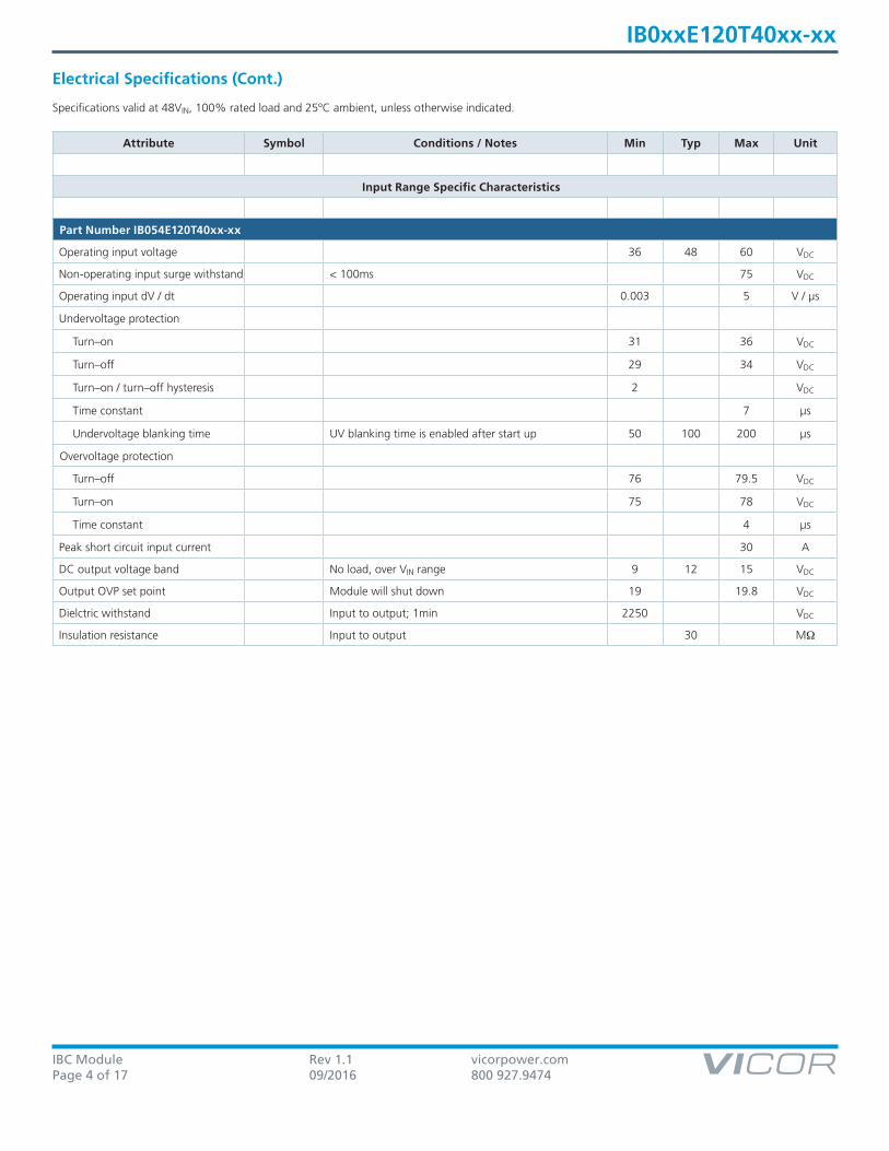
Part Number IB054E120T40xx-xx
Operating input voltage 36 48 60 VDC
Non-operating input surge withstand < 100ms 75 VDC
Operating input dV / dt 0.003 5 V / µs
Undervoltage protection
Turn–on 31 36 VDC
Turn–off 29 34 VDC
Turn–on / turn–off hysteresis 2 VDC
Time constant 7 µs
Undervoltage blanking time UV blanking time is enabled after start up 50 100 200 µs
Overvoltage protection
Turn–off 76 79.5 VDC
Turn–on 75 78 VDC
Time constant 4 µs
Peak short circuit input current 30 A
DC output voltage band No load, over VIN range 9 12 15 VDC
Output OVP set point Module will shut down 19 19.8 VDC
Dielctric withstand Input to output; 1min 2250 VDC
Insulation resistance Input to output 30 MΩ

IBC Module Rev 1.1 vicorpower.comPage 5 of 17 09/2016 800 927.9474
IB0xxE120T40xx-xx
Attribute Symbol Conditions / Notes Min Typ Max Unit
Common Input Specifications
Turn ON delay
Start-up inhibitVIN reaching turn-on voltage to enable function operational, see Figure 6
20 25 30 ms
Turn-on delayEnable to 10% VOUT; pre-applied VIN, 0 load capacitance, see Figure 7
50 µs
Output voltage rise timeFrom 10% to 90% VOUT, 10% load, 0 load capacitance. See Figure 8
50 µs
Restart turn-on delay See page 14 for restart after EN pin disable 250 ms
No load power dissipation
Enabled 3.0 3.9 W
Disabled 0.17 0.24 W
Input current Low line, full load 10.1 A
Inrush current overshoot Using test circuit in Figure 21, 15% load, high line 18 A
Input reflected ripple currentAt max power;Using test circuit in Figure 22; see Figure 5
400 mArms
Repetitive short circuit peak current 25 A
Internal input capacitance 8.8 µF
Internal input inductance 5 nH
Recommended external input capacitance
200nH maximum source inductance 47 470 µF
Electrical Specifications (Cont.)
Specifications valid at 48VIN, 100% rated load and 25ºC ambient, unless otherwise indicated.
IBC Module Rev 1.1 vicorpower.comPage 6 of 17 09/2016 800 927.9474
IB0xxE120T40xx-xx
Electrical Specifications (Cont.)
Specifications valid at 48VIN, 100% rated load and 25ºC ambient, unless otherwise indicated.
Attribute Symbol Conditions / Notes Min Typ Max Unit
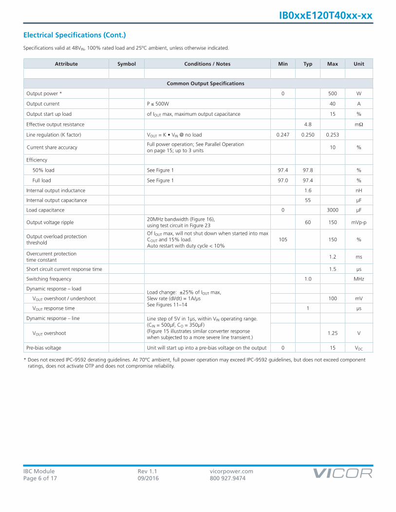
Common Output Specifications
Output power * 0 500 W
Output current P ≤ 500W 40 A
Output start up load of IOUT max, maximum output capacitance 15 %
Effective output resistance 4.8 mΩ
Line regulation (K factor) VOUT = K • VIN @ no load 0.247 0.250 0.253
Current share accuracyFull power operation; See Parallel Operationon page 15; up to 3 units
10 %
Efficiency
50% load See Figure 1 97.4 97.8 %
Full load See Figure 1 97.0 97.4 %
Internal output inductance 1.6 nH
Internal output capacitance 55 µF
Load capacitance 0 3000 µF
Output voltage ripple20MHz bandwidth (Figure 16),using test circuit in Figure 23
60 150 mVp-p
Output overload protection threshold
Of IOUT max, will not shut down when started into max COUT and 15% load. Auto restart with duty cycle < 10%
105 150 %
Overcurrent protection time constant
1.2 ms
Short circuit current response time 1.5 µs
Switching frequency 1.0 MHz
Dynamic response – loadLoad change: ±25% of IOUT max, Slew rate (dI/dt) = 1A/µs See Figures 11–14
VOUT overshoot / undershoot 100 mV
VOUT response time 1 µs
Dynamic response – line Line step of 5V in 1µs, within VIN operating range. (CIN = 500µF, CO = 350µF) (Figure 15 illustrates similar converter response when subjected to a more severe line transient.)
VOUT overshoot 1.25 V
Pre-bias voltage Unit will start up into a pre-bias voltage on the output 0 15 VDC
* Does not exceed IPC-9592 derating guidelines. At 70ºC ambient, full power operation may exceed IPC-9592 guidelines, but does not exceed component ratings, does not activate OTP and does not compromise reliability.

IBC Module Rev 1.1 vicorpower.comPage 7 of 17 09/2016 800 927.9474
IB0xxE120T40xx-xx
Attribute Symbol Conditions / Notes Min Typ Max Unit
Control & Interface Specifications
Enable (negative logic) Referenced to –IN
Module enable threshold 0.8 VDC
Module enable current VEN = 0.8V 130 200 µA
Module disable threshold 2.4 VDC
Modeule disable current VEN = 2.4V 130 µA
Disable hysteresis 500 mV
Enable pin open circuit voltage 2.5 3.0 VDC
EN to –IN resistance Open circuit, 10V applied between EN and –IN 35 kΩ
Enable (positive logic) Referenced to –IN
Module enable threshold 2.0 2.5 3.0 VDC
Module disable threshold 1.45 VDC
EN source current (operating) VEN = 5V 2 mA
EN voltage (operating) 4.7 5 5.3 VDC
Electrical Specifications (Cont.)
Specifications valid at 48VIN, 100% rated load and 25ºC ambient, unless otherwise indicated.
General Characteristics
• Conditions: TCASE = 25ºC, 75% rated load and specified input voltage range unless otherwise specified.
Attribute Symbol Conditions / Notes Min Typ Max Unit
MTBF Calculated per Telcordia SR-332, 40°C 1.0 Mhrs
Service life Calculated at 30°C 7 Years
Overtemperature shut downTJ ; Converter will reset when overtemperature condition is removed
125 130 135 ºC
Mechanical
Weight 0.71 / 20.3 oz / g
Length 2.30 / 58.4 in / mm
Width 0.9 / 22.9 in / mm
Height above customer board 0.39 / 9.9 in / mm
Pin solderability Storage life for normal solderability 1 Years
Moisture sensitivity level MSL Not applicable, for wave soldering only N/A
Clearance to customer board From lowest component on IBC 0.12 / 3.1 in / mm
Altitude, operatingDerate operating temp 1°C per 1000 feet above sea level
-500 10000 Feet
Relative humidity, operating Non condensing 10 90 %
RoHS compliance Compatible with RoHS directive 2002/95/EC
Agency approvals
UL/CSA 60950-1 cURus
UL/CSA 60950-1, EN60950-1 cTUVus
Low voltage directive (2006/95/EC) CE
IBC Module Rev 1.1 vicorpower.comPage 8 of 17 09/2016 800 927.9474
IB0xxE120T40xx-xx
Electrical Specifications (Cont.)
Specifications valid at 48VIN, 100% rated load and 25ºC ambient, unless otherwise indicated.
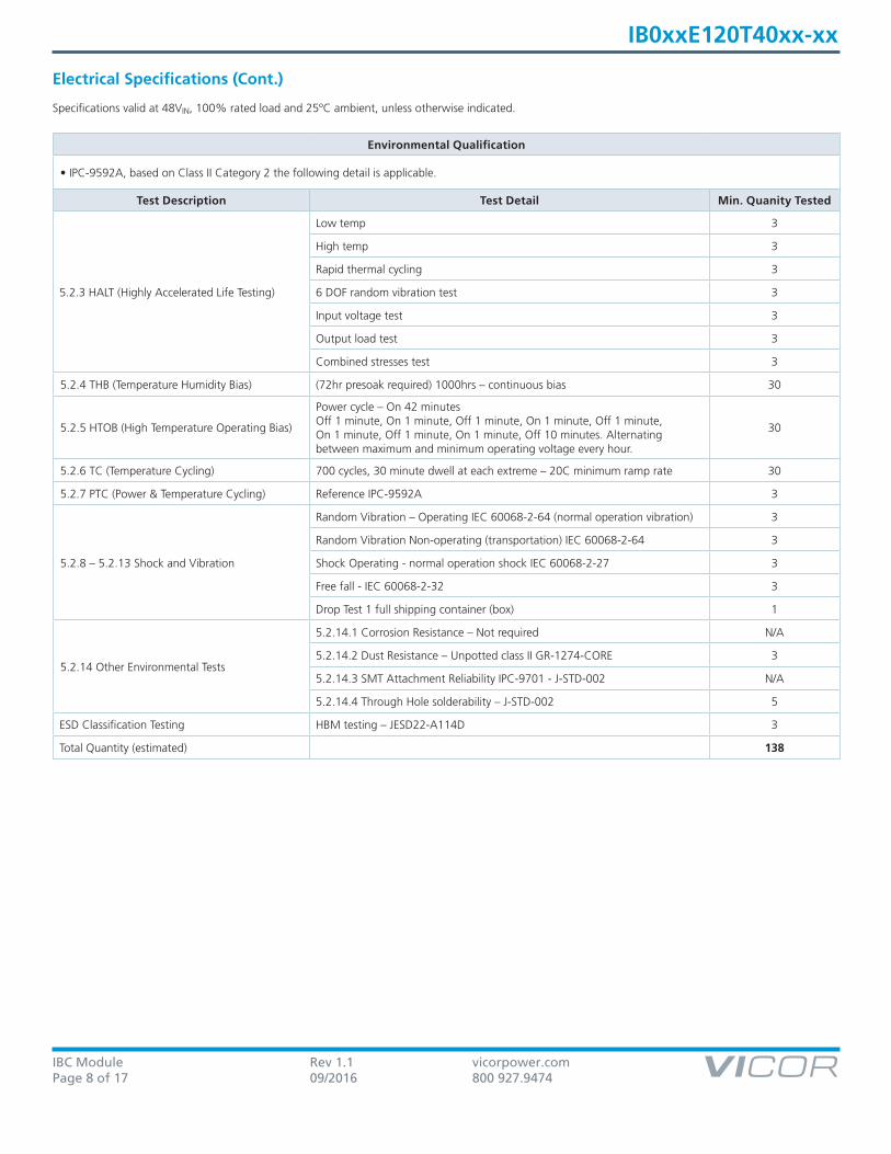
Environmental Qualification
• IPC-9592A, based on Class II Category 2 the following detail is applicable.
Test Description Test Detail Min. Quanity Tested
5.2.3 HALT (Highly Accelerated Life Testing)
Low temp 3
High temp 3
Rapid thermal cycling 3
6 DOF random vibration test 3
Input voltage test 3
Output load test 3
Combined stresses test 3
5.2.4 THB (Temperature Humidity Bias) (72hr presoak required) 1000hrs – continuous bias 30
5.2.5 HTOB (High Temperature Operating Bias)
Power cycle – On 42 minutesOff 1 minute, On 1 minute, Off 1 minute, On 1 minute, Off 1 minute, On 1 minute, Off 1 minute, On 1 minute, Off 10 minutes. Alternating between maximum and minimum operating voltage every hour.
30
5.2.6 TC (Temperature Cycling) 700 cycles, 30 minute dwell at each extreme – 20C minimum ramp rate 30
5.2.7 PTC (Power & Temperature Cycling) Reference IPC-9592A 3
5.2.8 – 5.2.13 Shock and Vibration
Random Vibration – Operating IEC 60068-2-64 (normal operation vibration) 3
Random Vibration Non-operating (transportation) IEC 60068-2-64 3
Shock Operating - normal operation shock IEC 60068-2-27 3
Free fall - IEC 60068-2-32 3
Drop Test 1 full shipping container (box) 1
5.2.14 Other Environmental Tests
5.2.14.1 Corrosion Resistance – Not required N/A
5.2.14.2 Dust Resistance – Unpotted class II GR-1274-CORE 3
5.2.14.3 SMT Attachment Reliability IPC-9701 - J-STD-002 N/A
5.2.14.4 Through Hole solderability – J-STD-002 5
ESD Classification Testing HBM testing – JESD22-A114D 3
Total Quantity (estimated) 138
IBC Module Rev 1.1 vicorpower.comPage 9 of 17 09/2016 800 927.9474
IB0xxE120T40xx-xx
Application Characteristics: WaveformsEf
ficie
ncy
(%)
IOUT (A)38V 48V 55VVIN:
92
93
94
95
96
97
98
99
0 8 16 24 32 40
Effic
ienc
y (%
)
IOUT (A)38V 48V 55VVIN:
92
93
94
95
96
97
98
99
0 8 16 24 32 40
Effic
ienc
y (%
)
IOUT (A)38V 48V 55VVIN:
92
93
94
95
96
97
98
99
0 8 16 24 32 40
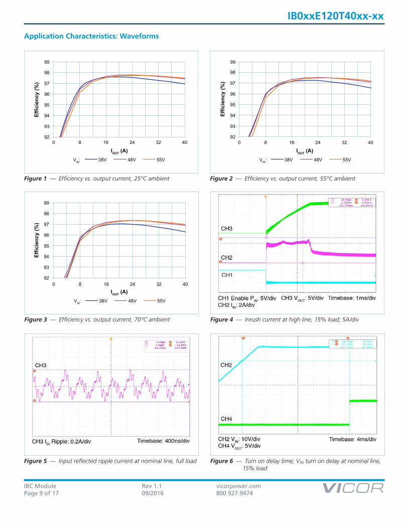
Figure 1 — Efficiency vs. output current, 25ºC ambient Figure 2 — Efficiency vs. output current, 55ºC ambient
Figure 3 — Efficiency vs. output current, 70ºC ambient
Figure 5 — Input reflected ripple current at nominal line, full load
Figure 4 — Inrush current at high line, 15% load; 5A/div
Figure 6 — Turn on delay time; VIN turn on delay at nominal line, 15% load

IBC Module Rev 1.1 vicorpower.comPage 10 of 17 09/2016 800 927.9474
IB0xxE120T40xx-xx
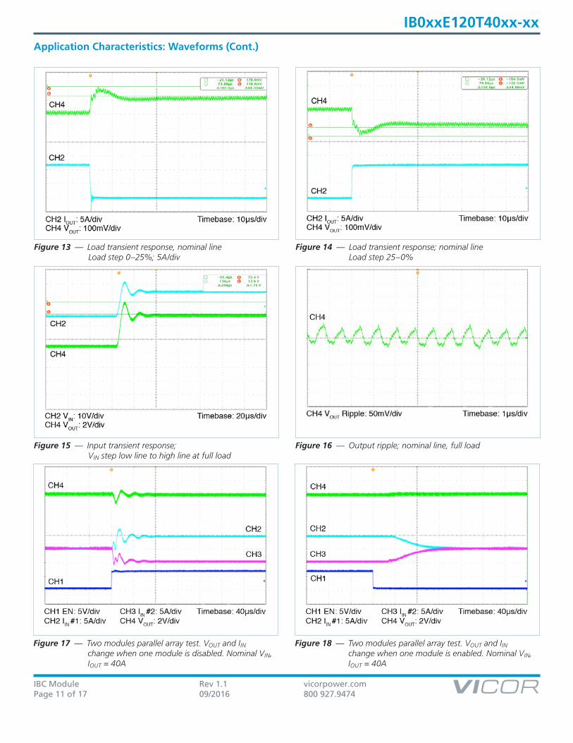
Application Characteristics: Waveforms (Cont.)
Figure 7 — Turn on delay time; enable turn on delay at nominal line, 15% load
Figure 8 — Output voltage rise time at nominal line, 10% load
Figure 9 — Overshoot at turn on at nominal line, 15% load Figure 10 — Undershoot at turn off at nominal line. 10% load
Figure 11 — Load transient response; nominal line Load step 75–100%
Figure 12 — Load transient response; full load to 75%; nominal line
IBC Module Rev 1.1 vicorpower.comPage 11 of 17 09/2016 800 927.9474
IB0xxE120T40xx-xx
Figure 15 — Input transient response; VIN step low line to high line at full load
Figure 16 — Output ripple; nominal line, full load
Figure 13 — Load transient response, nominal line Load step 0–25%; 5A/div
Figure 14 — Load transient response; nominal line Load step 25–0%
Application Characteristics: Waveforms (Cont.)
Figure 17 — Two modules parallel array test. VOUT and IIN change when one module is disabled. Nominal VIN, IOUT = 40A
Figure 18 — Two modules parallel array test. VOUT and IIN change when one module is enabled. Nominal VIN, IOUT = 40A

IBC Module Rev 1.1 vicorpower.comPage 12 of 17 09/2016 800 927.9474
IB0xxE120T40xx-xx
Application Characteristics: Waveforms (Cont.)O
utpu
t Cur
rent
(A)
Ambient Temperature (°C)200LFM 400LFM 600LFM
45
40
35
30
25
20
15
10
5
03525 45 55 65 75 85 95
Figure 19 — Maximum output current derating vs. ambient air temperature. Transverse airflow. Board and junction temperatures within IPC-9592 derating guidelines
Out
put C
urre
nt (A
)
Ambient Temperature (°C)200LFM 400LFM 600LFM
45
40
35
30
25
20
15
10
5
03525 45 55 65 75 85 95
Figure 20 — Maximum output current derating vs. ambient air temperature. Longitudinal airflow. Board and junction temperatures within IPC-9592 derating guidelines
Vsource
+
_
Current Probe
47µFIBC
+IN
EN
–IN
+OUT
–OUT
Load
C*
*Maximum load capacitance
Vsource
+
_
Current Probe
470µF IBC
+IN
EN
–IN
+OUT
–OUT
Load
10µH
Figure 21 — Test circuit; inrush current overshoot
+IN
–IN
+OUT
–OUT
IBC E – Load
Cy = 4700pF
20MHz BW
10µF 0.1µF
Cyb Cyd
CycCya
a-d
Figure 22 — Test circuit; input reflected ripple current
Figure 23 — Test circuit; output voltage ripple

IBC Module Rev 1.1 vicorpower.comPage 13 of 17 09/2016 800 927.9474
IB0xxE120T40xx-xx
Application Characteristics: Thermal Data
Figure 24 — Thermal plot, 200LFM, 25ºC, 48VIN, 450W output power
Figure 25 — Thermal plot, 200LFM, 25ºC, 48VIN, 450W output power
Figure 26 — Thermal plot, 400LFM, 25ºC, 48VIN, 450W output power
Figure 28 — Thermal plot, 600LFM, 25ºC, 48VIN, 450W output power
Figure 27 — Thermal plot, 400LFM, 25ºC, 48VIN, 450W output power
Figure 29 — Thermal plot, 600LFM, 25ºC, 48VIN, 450W output power
IBC Module Rev 1.1 vicorpower.comPage 14 of 17 09/2016 800 927.9474
IB0xxE120T40xx-xx
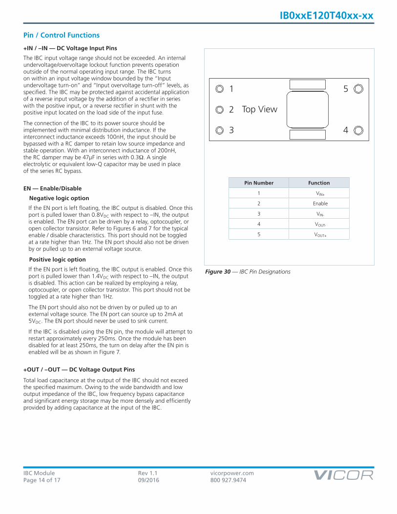
Pin / Control Functions
+IN / –IN — DC Voltage Input Pins
The IBC input voltage range should not be exceeded. An internal undervoltage/overvoltage lockout function prevents operation outside of the normal operating input range. The IBC turns on within an input voltage window bounded by the “Input undervoltage turn-on” and “Input overvoltage turn-off” levels, as specified. The IBC may be protected against accidental application of a reverse input voltage by the addition of a rectifier in series with the positive input, or a reverse rectifier in shunt with the positive input located on the load side of the input fuse.
The connection of the IBC to its power source should be implemented with minimal distribution inductance. If the interconnect inductance exceeds 100nH, the input should be bypassed with a RC damper to retain low source impedance and stable operation. With an interconnect inductance of 200nH, the RC damper may be 47µF in series with 0.3Ω. A single electrolytic or equivalent low-Q capacitor may be used in place of the series RC bypass.
EN — Enable/Disable
Negative logic option
If the EN port is left floating, the IBC output is disabled. Once this port is pulled lower than 0.8VDC with respect to –IN, the output is enabled. The EN port can be driven by a relay, optocoupler, or open collector transistor. Refer to Figures 6 and 7 for the typical enable / disable characteristics. This port should not be toggled at a rate higher than 1Hz. The EN port should also not be driven by or pulled up to an external voltage source.
Positive logic option
If the EN port is left floating, the IBC output is enabled. Once this port is pulled lower than 1.4VDC with respect to –IN, the output is disabled. This action can be realized by employing a relay, optocoupler, or open collector transistor. This port should not be toggled at a rate higher than 1Hz.
The EN port should also not be driven by or pulled up to an external voltage source. The EN port can source up to 2mA at 5VDC. The EN port should never be used to sink current.
If the IBC is disabled using the EN pin, the module will attempt to restart approximately every 250ms. Once the module has been disabled for at least 250ms, the turn on delay after the EN pin is enabled will be as shown in Figure 7.
+OUT / –OUT — DC Voltage Output Pins
Total load capacitance at the output of the IBC should not exceed the specified maximum. Owing to the wide bandwidth and low output impedance of the IBC, low frequency bypass capacitance and significant energy storage may be more densely and efficiently provided by adding capacitance at the input of the IBC.
Top View
1
2
3
5
4
Figure 30 — IBC Pin Designations
Pin Number Function
1 VIN+
2 Enable
3 VIN-
4 VOUT-
5 VOUT+

IBC Module Rev 1.1 vicorpower.comPage 15 of 17 09/2016 800 927.9474
IB0xxE120T40xx-xx
Applications Note
Parallel Operation
The IBC will inherently current share when operated in an array. Arrays may be used for higher power or redundancy in an application. Current sharing accuracy is maximized when the source and load impedance presented to each IBC within an array are equal. The recommended method to achieve matched impedances is to dedicate common copper planes within the PCB to deliver and return the current to the array, rather than rely upon traces of varying lengths. In typical applications the current being delivered to the load is larger than that sourced from the input, allowing narrower traces to be utilized on the input side if necessary. The use of dedicated power planes is, however, preferable.
One or more IBCs in an array may be disabled without adversely affecting operation or reliability as long as the load does not exceed the rated power of the enabled IBCs.
The IBC power train and control architecture allow bi-directional power transfer, including reverse power processing from the IBC output to its input. The IBC’s ability to process power in reverse improves the IBC transient response to an output load dump.
Thermal Considerations
The temperature distribution of the VI Brick® can vary significantly with its input / output operating conditions, thermal management and environmental conditions. Although the PCB is UL rated to 130°C, it is recommended that PCB temperatures be maintained at or below 125°C. For maximum long term reliability, lower PCB temperatures are recommended for continuous operation, however, short periods of operation at 125°C will not negatively impact performance or reliability.
WARNING: Thermal and voltage hazards. The IBC can operate with surface temperatures and operating voltages that may be hazardous to personnel. Ensure that adequate protection is in place to avoid inadvertent contact.
Input Impedance Recommendations
To take full advantage of the IBC capabilities, the impedance presented to its input terminals must be low from DC to approximately 5MHz. The source should exhibit low inductance and should have a critically damped response. If the interconnect inductance is excessive, the IBC input pins should be bypassed with an RC damper (e.g., 47µF in series with 0.3Ω) to retain low source impedance and proper operation. Given the wide bandwidth of the IBC, the source response is generally the limiting factor in the overall system response.
Anomalies in the response of the source will appear at the output of the IBC multiplied by its K factor. The DC resistance of the source should be kept as low as possible to minimize voltage deviations. This is especially important if the IBC is operated near low or high line as the overvoltage/undervoltage detection circuitry could be activated.
Input Fuse Recommendations
The IBC is not internally fused in order to provide flexibility in configuring power systems. However, input line fusing of VI Bricks must always be incorporated within the power system. A fast acting fuse should be placed in series with the +IN port.
Application Notes
For IBC and VI Brick application notes on soldering, thermal management, board layout, and system design visit www.vicorpower.com.

IBC Module Rev 1.1 vicorpower.comPage 16 of 17 09/2016 800 927.9474
IB0xxE120T40xx-xx
Top View
.153.8
2.300±.01058.42±.25
.153.8
.900±.01022.86±.25
.392±.0259.95±.64
TYPSEE CHART
.093
93) PL.2.36
.040
(3) PL.1.02
.386±.0259.80±.64
.123.1
.125
(2) PL.3.18
.060
(2) PL.1.52PIN LENGTH CHART
DESIGNATOR LENGTH
1 .145 [3.68]
2 .210 [5.33]
3 .180 [4.57]
2.000±.00350.80±.08
.300±.0037.62±.08
.300±.0037.62±.08
.080±.003
PLATED THRU HOLE.125±.003
[3.18±.08]ANNULAR RING
(3) PL.
2.03±.08.100±.003
PLATED THRU HOLE.180±.003
[4.57±.08]ANNULAR RING
(2) PL.
2.54±.08
1
2
3 4
5
Figure 31 — IBC outline drawing
Top View
.153.8
2.300±.01058.42±.25
.153.8
.900±.01022.86±.25
.392±.0259.95±.64
TYPSEE CHART
.093
93) PL.2.36
.040
(3) PL.1.02
.386±.0259.80±.64
.123.1
.125
(2) PL.3.18
.060
(2) PL.1.52PIN LENGTH CHART
DESIGNATOR LENGTH
1 .145 [3.68]
2 .210 [5.33]
3 .180 [4.57]
2.000±.00350.80±.08
.300±.0037.62±.08
.300±.0037.62±.08
.080±.003
PLATED THRU HOLE.125±.003
[3.18±.08]ANNULAR RING
(3) PL.
2.03±.08.100±.003
PLATED THRU HOLE.180±.003
[4.57±.08]ANNULAR RING
(2) PL.
2.54±.08
1
2
3 4
5
Figure 32 — IBC PCB recommended hole pattern
Mechanical Drawings
inch(mm)
inch(mm)
IBC Module Rev 1.1 vicorpower.comPage 17 of 17 09/2016 800 927.9474
IB0xxE120T40xx-xx
Vicor Corporation25 Frontage Road
Andover, MA, USA 01810Tel: 800-735-6200Fax: 978-475-6715
emailCustomer Service: [email protected]
Technical Support: [email protected]
Vicor’s comprehensive line of power solutions includes high density AC-DC and DC-DC modules and accessory components, fully configurable AC-DC and DC-DC power supplies, and complete custom power systems.
Information furnished by Vicor is believed to be accurate and reliable. However, no responsibility is assumed by Vicor for its use. Vicor makes no representations or warranties with respect to the accuracy or completeness of the contents of this publication. Vicor reserves the right to make changes to any products, specifications, and product descriptions at any time without notice. Information published by Vicor has been checked and is believed to be accurate at the time it was printed; however, Vicor assumes no responsibility for inaccuracies. Testing and other quality controls are used to the extent Vicor deems necessary to support Vicor’s product warranty. Except where mandated by government requirements, testing of all parameters of each product is not necessarily performed. Specifications are subject to change without notice.
Vicor’s Standard Terms and ConditionsAll sales are subject to Vicor’s Standard Terms and Conditions of Sale, which are available on Vicor’s webpage or upon request.
Product WarrantyIn Vicor’s standard terms and conditions of sale, Vicor warrants that its products are free from non-conformity to its Standard Specifications (the “Express Limited Warranty”). This warranty is extended only to the original Buyer for the period expiring two (2) years after the date of shipment and is not transferable. UNLESS OTHERWISE EXPRESSLY STATED IN A WRITTEN SALES AGREEMENT SIGNED BY A DULY AUTHORIZED VICOR SIGNATORY, VICOR DISCLAIMS ALL REPRESENTATIONS, LIABILITIES, AND WARRANTIES OF ANY KIND (WHETHER ARISING BY IMPLICATION OR BY OPERATION OF LAW) WITH RESPECT TO THE PRODUCTS, INCLUDING, WITHOUT LIMITATION, ANY WARRANTIES OR REPRESENTATIONS AS TO MERCHANTABILITY, FITNESS FOR PARTICULAR PURPOSE, INFRINGEMENT OF ANY PATENT, COPYRIGHT, OR OTHER INTELLECTUAL PROPERTY RIGHT, OR ANY OTHER MATTER.
This warranty does not extend to products subjected to misuse, accident, or improper application, maintenance, or storage. Vicor shall not be liable for collateral or consequential damage. Vicor disclaims any and all liability arising out of the application or use of any product or circuit and assumes no liability for applications assistance or buyer product design. Buyers are responsible for their products and applications using Vicor products and components. Prior to using or distributing any products that include Vicor components, buyers should provide adequate design, testing and operating safeguards.
Vicor will repair or replace defective products in accordance with its own best judgment. For service under this warranty, the buyer must contact Vicor to obtain a Return Material Authorization (RMA) number and shipping instructions. Products returned without prior authorization will be returned to the buyer. The buyer will pay all charges incurred in returning the product to the factory. Vicor will pay all reshipment charges if the product was defective within the terms of this warranty.
Life Support PolicyVICOR’S PRODUCTS ARE NOT AUTHORIZED FOR USE AS CRITICAL COMPONENTS IN LIFE SUPPORT DEVICES OR SYSTEMS WITHOUT THE EXPRESS PRIOR WRITTEN APPROVAL OF THE CHIEF EXECUTIVE OFFICER AND GENERAL COUNSEL OF VICOR CORPORATION. As used herein, life support devices or systems are devices which (a) are intended for surgical implant into the body, or (b) support or sustain life and whose failure to perform when properly used in accordance with instructions for use provided in the labeling can be reasonably expected to result in a significant injury to the user. A critical component is any component in a life support device or system whose failure to perform can be reasonably expected to cause the failure of the life support device or system or to affect its safety or effectiveness. Per Vicor Terms and Conditions of Sale, the user of Vicor products and components in life support applications assumes all risks of such use and indemnifies Vicor against all liability and damages.
Intellectual Property NoticeVicor and its subsidiaries own Intellectual Property (including issued U.S. and pending patent applications) relating to the products described in this data sheet. No license, whether express, implied, or arising by estoppel or otherwise, to any intellectual property rights is granted by this document. Interested parties should contact Vicor’s Intellectual Property Department.
The products described on this data sheet are protected by the following U.S. Patents Numbers:5,945,130; 6,403,009; 6,710,257; 6,911,848; 6,930,893; 6,934,166; 6,940,013; 6,969,909; 7,038,917; 7,145,786; 7,166,898; 7,187,263; 7,361,844; D496,906; D505,114; D506,438; D509,472; and for use under 6,975,098 and 6,984,965.