ibrahim mark - university of waterloo
TRANSCRIPT

CMOS Transimpedance Amplifier for
Biosensor Signal Acquisition
by
Mark Ibrahim
A thesis
presented to the University of Waterloo
in fulfillment of the
thesis requirement for the degree of
Master of Applied Science
in
Electrical and Computer Engineering
Waterloo, Ontario, Canada, 2014
c© Mark Ibrahim 2014


I hereby declare that I am the sole author of this thesis. This is a true copy of the thesis,
including any required final revisions, as accepted by my examiners.
I understand that my thesis may be made electronically available to the public.
iii

Abstract
A 1-GΩ CMOS transimpedance amplifier (TIA) suitable for processing sub-nA-level
currents in electrochemical biosensor signal-acquisition circuits is presented. Use of a two-
stage active transconductor provides resistive feedback in place of a large-area linear resis-
tor. The TIA feedback loop is engineered to suppress output offset caused by DC input
leakage currents of ±0.9 nA. A mechanism to tune the low-frequency cutoff of the TIA
from 0.7 Hz to 500 Hz is implemented which permits operation under variable environ-
mental conditions. Simulated and experimental results from a custom TIA fabricated in a
3.3-V 0.35-µm CMOS process are presented.
v

Acknowledgements
I would like to thank all the people who made this thesis possible. First, I would
like to thank my supervisor, Professor Peter Levine, for his mentorship, encouragement
and patience throughout my graduate studies. My thanks to Professor David Nairn and
Professor Slim Boumaiza for serving as my thesis readers as well as for their constructive
feedback.
I would also like to thank my peers including Ayman, Alex, and Areeb. Thank you for
all the time I had to bounce ideas off you and help with debugging.
Many people outside the group have helped me through my Master’s. I would like
acknowledge my friends for giving me someone to vent to and reinvigorate me throughout
my studies.
Finally, I am indebted to my parents for their unconditional support in my endeavours.
This thesis would not have been possible without them.
vi


Dedication
This thesis is dedicated to the kids and youth at St. Mary’s Coptic Orthodox Church
in Kitchener.
viii


Table of Contents
List of Tables xv
List of Figures xvii
1 Introduction 1
1.1 Outline . . . . . . . . . . . . . . . . . . . . . . . . . . . . . . . . . . . . . . 6
2 Review of Transimpedance Amplifiers 8
2.1 Resistor-Feedback Transimpedance Amplifier . . . . . . . . . . . . . . . . . 9
2.1.1 Gain and Bandwidth . . . . . . . . . . . . . . . . . . . . . . . . . . 9
2.1.2 Output Voltage Saturation . . . . . . . . . . . . . . . . . . . . . . . 11
2.1.3 Noise Performance . . . . . . . . . . . . . . . . . . . . . . . . . . . 11
2.1.4 Design Tradeoffs . . . . . . . . . . . . . . . . . . . . . . . . . . . . 12
2.2 Capacitive Transimpedance Amplifier . . . . . . . . . . . . . . . . . . . . . 13
2.2.1 Gain and Bandwidth . . . . . . . . . . . . . . . . . . . . . . . . . . 14
2.2.2 Output Voltage Saturation . . . . . . . . . . . . . . . . . . . . . . . 15
x

2.2.3 Noise Performance . . . . . . . . . . . . . . . . . . . . . . . . . . . 16
2.2.4 Design Tradeoffs . . . . . . . . . . . . . . . . . . . . . . . . . . . . 17
2.3 Resistive-Feedback Transimpedance Amplifier with Proportional-integrative
Amplifier . . . . . . . . . . . . . . . . . . . . . . . . . . . . . . . . . . . . . 18
2.3.1 Gain and Bandwidth . . . . . . . . . . . . . . . . . . . . . . . . . . 19
2.3.2 Output Voltage Saturation . . . . . . . . . . . . . . . . . . . . . . . 20
2.3.3 Noise Performance . . . . . . . . . . . . . . . . . . . . . . . . . . . 21
2.3.4 Design Tradeoffs . . . . . . . . . . . . . . . . . . . . . . . . . . . . 22
2.4 Continuous Active Reset TIA . . . . . . . . . . . . . . . . . . . . . . . . . 22
2.4.1 Gain and Bandwidth . . . . . . . . . . . . . . . . . . . . . . . . . . 23
2.4.2 Active Resistor Design . . . . . . . . . . . . . . . . . . . . . . . . . 28
2.4.3 Output Voltage Saturation . . . . . . . . . . . . . . . . . . . . . . . 30
2.4.4 Noise Performance . . . . . . . . . . . . . . . . . . . . . . . . . . . 30
2.4.5 Design Tradeoffs . . . . . . . . . . . . . . . . . . . . . . . . . . . . 31
2.5 Performance Comparison of TIA Architectures . . . . . . . . . . . . . . . . 32
3 Proposed Transimpedance Amplifier Architecture 33
3.1 Selecting the Feedback Type . . . . . . . . . . . . . . . . . . . . . . . . . . 33
3.2 Feedback Transconductor Implementation . . . . . . . . . . . . . . . . . . 35
3.2.1 Noise Performance . . . . . . . . . . . . . . . . . . . . . . . . . . . 38
3.3 Low-Frequency Input Signal Suppression . . . . . . . . . . . . . . . . . . . 38
xi

3.3.1 Bandwidth Tuning . . . . . . . . . . . . . . . . . . . . . . . . . . . 41
3.4 Comparison of Proposed TIA with other Architectures . . . . . . . . . . . 45
4 Circuit Design and Implementation 47
4.1 Bandwidth Tuning . . . . . . . . . . . . . . . . . . . . . . . . . . . . . . . 49
4.2 Transconductor Design . . . . . . . . . . . . . . . . . . . . . . . . . . . . . 50
4.2.1 Resistor Layout . . . . . . . . . . . . . . . . . . . . . . . . . . . . . 50
4.3 Amplifier Design . . . . . . . . . . . . . . . . . . . . . . . . . . . . . . . . 52
4.3.1 Design of Amplifier A1 . . . . . . . . . . . . . . . . . . . . . . . . . 54
4.3.2 Design of Amplifier A2 . . . . . . . . . . . . . . . . . . . . . . . . . 58
4.3.3 Design of Amplifier A3 and A4 . . . . . . . . . . . . . . . . . . . . . 61
4.3.4 Output Buffers . . . . . . . . . . . . . . . . . . . . . . . . . . . . . 63
4.3.5 Bias Circuit . . . . . . . . . . . . . . . . . . . . . . . . . . . . . . . 65
4.3.6 Summary . . . . . . . . . . . . . . . . . . . . . . . . . . . . . . . . 66
4.4 Stability . . . . . . . . . . . . . . . . . . . . . . . . . . . . . . . . . . . . . 67
4.5 System Simulation . . . . . . . . . . . . . . . . . . . . . . . . . . . . . . . 68
5 Experimental Results 71
5.1 Test Apparatus . . . . . . . . . . . . . . . . . . . . . . . . . . . . . . . . . 72
5.2 Measured Results from TIA Chip . . . . . . . . . . . . . . . . . . . . . . . 75
5.2.1 Frequency Response . . . . . . . . . . . . . . . . . . . . . . . . . . 75
xii

5.2.2 Linearity . . . . . . . . . . . . . . . . . . . . . . . . . . . . . . . . . 76
5.2.3 Noise . . . . . . . . . . . . . . . . . . . . . . . . . . . . . . . . . . . 78
5.2.4 Transient Response . . . . . . . . . . . . . . . . . . . . . . . . . . . 79
5.3 Performance Comparison . . . . . . . . . . . . . . . . . . . . . . . . . . . . 80
6 Conclusion 82
6.1 Contributions . . . . . . . . . . . . . . . . . . . . . . . . . . . . . . . . . . 82
6.2 Future Work . . . . . . . . . . . . . . . . . . . . . . . . . . . . . . . . . . . 83
6.2.1 Additional Transconductor Stages . . . . . . . . . . . . . . . . . . . 83
6.2.2 Parasitic Capacitance . . . . . . . . . . . . . . . . . . . . . . . . . . 83
6.3 Improvements . . . . . . . . . . . . . . . . . . . . . . . . . . . . . . . . . . 84
6.3.1 Reduced Noise . . . . . . . . . . . . . . . . . . . . . . . . . . . . . 84
6.3.2 Transimpedance Variation . . . . . . . . . . . . . . . . . . . . . . . 84
APPENDICES 86
A Design of PCB for Testing 87
References 92
xiii


List of Tables
2.1 Summary of performance for various TIA architectures. . . . . . . . . . . . 32
4.1 Summary of performance for various TIA architectures. . . . . . . . . . . . 48
4.2 Aspect ratio of bias transistors for each amplifier. All dimensions in µm. . 66
4.3 Simulated performance of individual amplifiers in TIA. . . . . . . . . . . . 67
5.1 Specifications for amplifiers used in discrete current source of Fig 5.2. . . . 73
5.2 Summary of performance for various TIA architectures in comparison with
the presented work. . . . . . . . . . . . . . . . . . . . . . . . . . . . . . . . 81
A.1 Mapping table for chip pins. . . . . . . . . . . . . . . . . . . . . . . . . . . 90
xv


List of Figures
1.1 Gating in single sodium channels: Patch clamp recording of unitary Na
currents in a toe muscle of adult mouse. (a) Applied voltage step from -80
to -40 mV. Ion channels are closed prior to initial voltage step. (b) Current
transient response for a single patch containing over 10 sodium channels.
(c) The ensemble mean of 352 repetitions of the single patch current. . . . 2
1.2 (a) Conventional whole-cell patch clamp recording using discrete TIA. A
skilled technician uses pipette and micromanipulator to probe the cell. (b)
Planar patch clamp system where the pipette electrode is replaced with a
CMOS micro-pore electrode. Cells adhere to the aperture using suction.
TIA is also integrated in CMOS . . . . . . . . . . . . . . . . . . . . . . . . 3
1.3 Block diagram for a typical electrochemical biosensor. . . . . . . . . . . . . 5
2.1 Transimpedance amplifier with linear feedback resistor. . . . . . . . . . . . 10
2.2 A conventional capacitive transimpedance amplifier with a parallel reset
switch. . . . . . . . . . . . . . . . . . . . . . . . . . . . . . . . . . . . . . . 13
2.3 CTIA transfer function for (a) varying values of Tint (Cf = 100 fF) and (b)
varying values of Cf (Tint = 100 µs). . . . . . . . . . . . . . . . . . . . . . 15
xvii

2.4 Parallel MOS reset switch in CTIA modeled as ideal switch with series on
resistance Ron. . . . . . . . . . . . . . . . . . . . . . . . . . . . . . . . . . . 16
2.5 RTIA-PI circuit architecture. PI controller added in feedback loop to atten-
uate effects of input DC current at the output. . . . . . . . . . . . . . . . . 19
2.6 Frequency magnitude response of the resistive feedback TIA with PI con-
troller shown in Figure 2.5. . . . . . . . . . . . . . . . . . . . . . . . . . . . 21
2.7 Continuous active reset TIA schematic. Consists of integrator stage similar
to the RTIA-PI followed by a second differentiator stage. . . . . . . . . . . 23
2.8 Magnitude response of the H(s) amplifier within the integrator stage of the
CARTIA in Figure 2.7. . . . . . . . . . . . . . . . . . . . . . . . . . . . . . 24
2.9 Frequency magnitude response of the active reset integrator stage of the
TIA in Figure 2.7. . . . . . . . . . . . . . . . . . . . . . . . . . . . . . . . 25
2.10 Frequency magnitude response of the differentiator stage of the TIA in Fig-
ure 2.7. . . . . . . . . . . . . . . . . . . . . . . . . . . . . . . . . . . . . . . 26
2.11 Frequency magnitude response of the continuous active reset stage of the
TIA in Figure 2.7 as a result of cascading an integrator with a differentiator. 27
2.12 Circuit implementation of amplifier H(s) for the CARTIA shown in Figure 2.7. 28
2.13 Schematic of current divider cell (dashed box, Iout/Iin) as the core of a
high-linearity full-swing transconductor circuit Iout/Vin. . . . . . . . . . . . 29
3.1 Transimpedance amplifier with feedback transconductor. . . . . . . . . . . 35
3.2 Transimpedance amplifier with two-stage feedback transconductor. . . . . . 36
3.3 Transimpedance amplifier architecture with feedback transconductor and
integrator to suppress input currents below the low-frequency cutoff. . . . . 40
xviii

3.4 Expected frequency magnitude response of the proposed TIA. . . . . . . . 40
3.5 Transimpedance amplifier with transconductor feedback and integrator to
suppress input currents below the low-frequency cutoff. . . . . . . . . . . . 41
3.6 Diode-connected PMOS pseudo-resistor, where the gate-drain and source-
body terminals are shorted. . . . . . . . . . . . . . . . . . . . . . . . . . . 42
3.7 Transient simulation of VGS for PMOS pseudo-resistor shown in Figure 3.6. 43
3.8 (a) IDS vs VDS curve in the 0.35-µm CMOS technology of a diode-connected
PMOS transistor with width and length of 4 µm and 2 µm, respectively.
Terminal pairs gate-drain and source-body are shorted. (b) The effective
resistance of the diode-connected PMOS. Calculated by taking the derivative
of (a) and inverting (dVGS/dIin). The sharp drop in resistance at 0 V is a
result of the numerical modeling of the simulator. . . . . . . . . . . . . . . 44
3.9 PMOS devices connected in series to reduce distortion by subdividing ap-
plied voltage equally across all devices operating (a) as diode-connected
PMOS/lateral BJT devices and (b) in the subthreshold regime with an ap-
plied control voltage VCTRL. . . . . . . . . . . . . . . . . . . . . . . . . . . 44
3.10 Simulation of (a) the IDS vs. VDS curve and (b) effective resistance under
various control voltages (Vctrl) for a single subthreshold PMOS device. . . . 45
4.1 Transimpedance amplifier with transconductor feedback and PI controller
to suppress input currents below the low-frequency cutoff. . . . . . . . . . 48
4.2 Simulated tuning range of the TIA low-frequency cutoff. . . . . . . . . . . 49
4.3 P+ diffusion resistor layout of Rb interspersed throughout MRb. . . . . . . 51
4.4 Circuit schematic for general folded-cascode amplifier. . . . . . . . . . . . . 53
xix

4.5 Circuit schematic for amplifier A1 with channel widths specified. All tran-
sistors have a channel length of 1 µm. . . . . . . . . . . . . . . . . . . . . 56
4.6 Open-loop frequency response of amplifier A1a. . . . . . . . . . . . . . . . 56
4.7 Open-loop frequency response of amplifier A1. . . . . . . . . . . . . . . . . 57
4.8 Differential voltage transfer characteristic of amplifier A1. . . . . . . . . . 57
4.9 Circuit schematic for three-stage amplifier A2 with channel widths specified.
All transistors have a channel length of 2 µm. . . . . . . . . . . . . . . . . 59
4.10 Open-loop frequency response of amplifier A2. . . . . . . . . . . . . . . . . 60
4.11 Differential voltage transfer characteristic of amplifier A2. . . . . . . . . . 60
4.12 Circuit schematic for cascode amplifier A3 with output buffer stage. Ampli-
fier A4 is identical except without the buffer stage composed of M6 and M7.
Channel widths are specified. All transistors have a channel length of 1 µm. 61
4.13 Open-loop frequency response of amplifier A3. . . . . . . . . . . . . . . . . 62
4.14 Open-loop frequency response of amplifier A4. . . . . . . . . . . . . . . . . 62
4.15 Differential voltage transfer characteristic of amplifier A3. . . . . . . . . . 63
4.16 Differential voltage transfer characteristic of amplifier A4. . . . . . . . . . 63
4.17 Circuit schematic for two-stage amplifier used for unity-gain feedback buffers
at TIA output nodes Vout and Vx. All transistors have a channel length of 1
µm. . . . . . . . . . . . . . . . . . . . . . . . . . . . . . . . . . . . . . . . . 64
4.18 Open-loop frequency response of unity-gain buffer. . . . . . . . . . . . . . 64
4.19 Current mirror circuit used to bias cascode amplifiers A1, A2, A3, and A4 . 65
xx

4.20 Loop gain magnitude (a) and phase (b) of the system shown in Figure 4.1
for various values of Vctrl . . . . . . . . . . . . . . . . . . . . . . . . . . . . 69
4.21 Transimpedance magnitude of the system shown in Figure 4.1 for various
values of Vctrl. . . . . . . . . . . . . . . . . . . . . . . . . . . . . . . . . . . 70
5.1 Chip photo showing key TIA components. . . . . . . . . . . . . . . . . . . 71
5.2 Discrete current source used to provide a controllable current to the TIA
under test. A discrete TIA to calibrate current source is also shown. . . . . 72
5.3 Frequency response of the discrete test TIA driven by current source in
Figure 5.2. . . . . . . . . . . . . . . . . . . . . . . . . . . . . . . . . . . . . 74
5.4 Measured transimpedance over frequency with variable low-frequency cutoff. 75
5.5 Simulated and measured tuning range of the TIA low-frequency cutoff. . . 76
5.6 Measured relative linearity error of the TIA with an ac input current. . . . 77
5.7 TIA output voltage Vout and internal node Vx as a function of dc input current. 78
5.8 Measured input-referred current noise PSD of the TIA. . . . . . . . . . . . 79
5.9 Response of the TIA as a result of a 40 pA step input current. The low-
frequency cutoff of the TIA has been set to 200 Hz. . . . . . . . . . . . . . 80
A.1 Discrete voltage divider circuit used to generate off chip voltages. . . . . . 88
A.2 Bonding diagram of TIA for CQFP44A package. . . . . . . . . . . . . . . . 89
A.3 Test board circuit schematic the fabricated chip. . . . . . . . . . . . . . . . 91
A.4 Physical layout of PCB for testing the fabricated chip. . . . . . . . . . . . 91
xxi


Chapter 1
Introduction
Transimpedance amplifiers (TIAs) are integral components of complementary metal-oxide-
semiconductor (CMOS) integrated low-current measurement systems. Resistor and capacitor-
based TIAs for processing nA-level currents and below have found numerous applications
in CMOS electrochemical biosensors, including patch-clamp electrophysiology chips [1][2],
integrated nanopore and ion channel sensors [3][4][5], and on-chip electrochemical DNA
sensor arrays [6][7].
Patch clamp electrophysiology is a technique used to measure the current that flows
through a cell membrane which has applications in drug discovery and research for phar-
maceutical development [2]. Ion channels along the cell membrane control the flow of ions
in and out of the cell which gives rise to a current. Ion channels are categorized by the way
in which they are gated, that is, ion channels are open or closed by different mechanisms.
Voltage-gated ion channels react to changes in the membrane potential while ligand-gated
channels are open or blocked in response to binding chemical messengers [8]. A single ion
channel generates a short current pulse while the sum of multiple ion channels can produce
1

larger pulses as shown in Figure 1.1. These transient signal currents generated by the flow
Figure 1.1: Gating in single sodium channels: Patch clamp recording of unitary Na currents
in a toe muscle of adult mouse. (a) Applied voltage step from -80 to -40 mV. Ion channels
are closed prior to initial voltage step. (b) Current transient response for a single patch
containing over 10 sodium channels. (c) The ensemble mean of 352 repetitions of the single
patch current [9][10].
of ions are in the pA to nA range and require a typical recording bandwidth ranging from
1 Hz to 10 kHz [11].
Electrophysiologists are interested in measuring the amplitude, duration and frequency
of the current pulses generated by ion channels to determine the effects of foreign substances
and/or pharmaceutical compounds. Additionally, patch clamp is a primary tool in the
2

study of genetic disorders which disrupt normal functioning ion channels such as cystic
fibrosis, fibromyalgia, and epilepsy [12][13][14].
Figure 1.2(a) shows a traditional patch clamp system. The cell of interest lies within
an electrolyte that is biased to a reference voltage. A micro-pipette with an embedded
electrode is clamped over a single ion channel and is connected to the TIA. Small currents
flow through the large feedback resistor in the TIA to develop an output voltage.
Figure 1.2: (a) Conventional whole-cell patch clamp recording using discrete TIA. A skilled
technician uses pipette and micromanipulator to probe the cell. (b) Planar patch clamp
system where the pipette electrode is replaced with a CMOS micro-pore electrode. Cells
adhere to the aperture using suction. TIA is also integrated in CMOS [1].
Patch clamp systems on chip can be realized by implementing the TIA in a CMOS
process. Conventional patch clamping is a labour intensive process is carried out by skilled
technicians with the use of micro-pipette to probe the cell membrane and as a result it is a
costly and slow process [15]. However, a planar patch clamp system can be developed using
CMOS electrodes as shown in Figure 1.2(b) [16]. By integrating the signal acquisition
3

circuitry (TIA and any proceeding stages) with the electrode in CMOS, large arrays of
biosensor systems can be developed to reduce costs and increase measurement throughput.
A second application of TIAs for biosensor signal acquisition is in impedance spec-
troscopy. This is a small-signal technique which involves applying an AC voltage to a
biochemical specimen over a range of frequencies while measuring the resulting ac current.
Using these quantities, changes in the electrical impedance can be related to physiological
changes in the specimen [17].
Figure 1.3 shows a typical electrochemical biosensor signal acquisition system consisting
of an electrochemical interface and signal acquisition circuit. The interface is represented
by an electrical model of the working electrode, electrolyte which sustains the biochemical
reaction of interest, and test specimen [18]. The biochemical reaction or specimen is
modeled with the current source is which represents the input signal of interest along with
parallel resistance and capacitance Rp and Cp respectively which, in the case of patch
clamp, models the cell membrane. RWE and CWE represent the impedance of the interface
between the biochemical reaction site and working electrode. While the TIA drives the
working electrode to virtual ground, VGND, a secondary voltage source, VREF , is required
to bias the electrolyte in order to establish a potential difference between the electrolyte
and the working electrode. As a result of the applied potential, freely moving ions readily
available in the electrolyte interact with the working electrode and give rise to a standing
(DC) current applied to the TIA. This current leakage between the electrolyte and the
electrode is illustrated by the signal path from VREF through Rp and RWE.
DC currents may be inherent to the signal source is. For example, in whole-cell patch
clamp applications, the total current measured through the cell membrane is a result of the
cumulative effect of hundreds of ion channels opening and closing [19]. Each type of ion
channel is responsible for regulating the concentration of a particular ion on either side of
4

Figure 1.3: Block diagram for a typical electrochemical biosensor.
the cell membrane [20]. There exists passive ion channels which are continuously passing
current through the cell membrane that gives rise to an average or DC leakage current on
the order of nA [21][22].
In the biosensor signal acquisition circuit shown in Figure 1.3, the TIA holds the working
electrode at virtual ground and converts the bidirectional input signal current iin to an
amplified voltage. The TIA may be followed by additional gain stages, filters, and an
analog-to-digital converter (ADC) to enable further gain and signal processing. Each
additional stage injects noise into the system until the measured signal is digitized, at
which point it is essentially immune to noise. The TIA must provide high gain to reduce
input-referred noise so that an adequate signal-to-noise ratio (SNR) can be achieved.
A desirable function of the TIA is to prevent the passage of large offset voltage caused by
DC input current produced by the biochemical process under investigation and external
low-frequency interference. Output offset voltage can saturate subsequent amplification
stages of the acquisition circuit, reducing the dynamic range of the measurement system.
While AC coupling subsequent stages can prevent saturation, integration of large DC-
blocking capacitors may be impractical in some applications due to chip area constraints.
To combat this issue, a CMOS integrator-differentiator-based TIA with a continuous-time
capacitor reset network for impedance spectroscopy has previously been reported which
5

prevents saturation of the first-stage integrator [23]. In addition, a TIA constructed from
discrete components for semiconductor radiation detection has been reported which uses
a proportional-integral control amplifier in the feedback path to zero the DC level of the
TIA output [24].
This thesis presents a 1-GΩ CMOS resistive-feedback TIA with adjustable low-frequency
cutoff. The proposed design is intended for use in electrochemical impedance spectroscopy
(EIS) biosensor applications to record nA-level AC currents in the 1-Hz to 1-kHz range.
Unlike [24], this TIA is amenable to CMOS integration because a two-stage op-amp-based
transconductor [25] is integrated in the feedback path to achieve 1-GΩ transimpedance.
Use of a single linear resistor to achieve such high gain would consume excessive chip area.
While [23] and [24] are effective in reducing TIA output offset, no mechanism is provided
to adjust the low-frequency cutoff in order to adapt to changes in input-signal bandwidth or
measurement conditions. However, frequency tuning is supported in the proposed design by
adjusting a MOS active resistor through gate-voltage control within the TIA feedback loop.
The ability to dynamically adjust the low-frequency cutoff is unique to this design and has
several applications in biosensor signal acquisition systems. For patch clamp applications,
bandwidth tuning allows for selective measurement of the membrane current by filtering out
the effects of passive and other high-conductance ion channels. Additionally, interference
can be filtered out, such as 60 Hz line interference that may couple to the electrolyte
potential or the TIA bias.
1.1 Outline
This thesis is structured as follows: Chapter 2 reviews several TIA architectures and pro-
vides background on design considerations and constraints. Popular techniques for current
6

to voltage amplification are also discussed. Chapter 3 builds upon the TIAs discussed
in Chapter 2 and other system-level design decisions to present a unique TIA architec-
ture. Circuit design and implementation details of the TIA are discussed in Chapter 4. In
Chapter 5, the experimental results from the proposed TIA implemented in a five-metal,
double-poly, 0.35-µm CMOS process are presented. Chapter 6 concludes the thesis and
discusses improvements to the chip design and future work.
7

Chapter 2
Review of Transimpedance
Amplifiers
TIAs are generally used as the first stage of low-current sensor interfaces like the one
shown in Figure 1.3. The TIA is designed to provide sufficient gain so that the input
signal is within the input range of the ADC after passing through subsequent gain and
filtering stages. The TIA must contribute minimal noise since the first stage of any signal
acquisition system has the greatest effect on the SNR [26].
As discussed in Chapter 1, the DC offset at the TIA output must be reduced to prevent
saturation of the following stages of the acquisition channel. The input signals for the
applications described in Chapter 1 consist of a standing (DC) current IIN and an AC
signal current of interest iin. In this thesis, IIN is defined for signal currents below 100
Hz while iin represents signal currents above 100 Hz. With respect to TIAs, IIN and iin
stimulate the system to produce DC and AC signal voltages VOUT and vout, respectively.
This chapter provides background information on TIAs. Sections 2.1 and 2.2 review
8

classical TIAs with resistive feedback and capacitive feedback, respectively. Sections 2.3
and 2.4 comprise a short literature review of two additional TIA architectures that inspired
the work of this thesis.
2.1 Resistor-Feedback Transimpedance Amplifier
A conventional resistor-feedback TIA (RTIA) is shown in Figure 2.1 where input signal
current iIN flows through resistor Rf in the feedback path, providing an output voltage
vOUT . The operational amplifier (op amp) input resistance is assumed to be large enough
such that any input bias current drawn by the op amp is several orders of magnitude less
than the input current. The transfer function of the TIA is given by
vOUT
iIN
(s) = − A(s)
1 + A(s)
Rf
1 + sRfCp
, (2.1)
where A(s) is the op amp open-loop frequency response and Cp is the parasitic capaci-
tance that exists between the inverting input and output. Capacitance Cp can limit the
bandwidth of the TIA as suggested by the equation above. For DC input signals, the
transimpedance becomes VOUT/IIN ≈ −Rf .
2.1.1 Gain and Bandwidth
To obtain further insight into the frequency response of the TIA in Figure 2.1, A(s) is
modeled with a single-pole roll-off:
A(s) =A0
1 + s/ω0
, (2.2)
9

Figure 2.1: Transimpedance amplifier with linear feedback resistor.
where A0 is the open-loop DC gain of the op amp and ω0 is the -3-dB cutoff frequency.
Eq. (3.2) can be rewritten as
vOUT
iIN
≈ − A0
1 + A0
Rf
[1 + s/(A0ω0)][1 + sRfCp], (2.3)
where A0ω0 is the gain-bandwidth product (GBP) of the op amp.
As evident from the denominator of Eq. (2.3), the pole frequencies, fp1 and fp2 (in Hz)
of the TIA with resistive feedback are given by
fp1 =1
2πω0A0
and fp2 =1
2πRfCp
. (2.4)
The dominant pole is dependent on the choice of components. If the GBP of the op amp is
sufficiently large, which is usually the case, fp2 is lower than fp1 and the 3-dB bandwidth
is determined by the choice of Rf and parasitic capacitance Cp.
Here the tradeoff between gain and bandwidth is apparent. Increasing Rf will increase
the transimpedance of the TIA at the expense of reduced bandwidth. In the case of a
discrete component implementation, Cp is mostly a result of the resistor package, circuit
board parasitics, and the op amp.
10

2.1.2 Output Voltage Saturation
The non-inverting terminal of the TIA in Figure 2.1 is connected to a constant virtual
ground voltage VGND which is often set midway between the op amp power supply rails
VDD and VSS. If the input current has a zero DC component, then there is no DC voltage
drop across Rf and the output voltage node is set to the mid-rail voltage. In this way,
signal currents are provided with maximum headroom, assuming the output swing of the
op amp is symmetric about zero. However, when a positive DC input current IIN flows,
then
VOUT = −RfIIN + VGND. (2.5)
VOUT may saturate near VSS depending on the magnitude of IIN and the value of Rf .
Likewise, VOUT may saturate at VDD when IIN becomes sufficiently negative. In either
case, when VOUT has saturated, input signal currents will either be clipped or undetectable
by the TIA.
2.1.3 Noise Performance
The main source of noise in the RTIA is the thermal noise generated by Rf which is given
by
i2Rf(f) =
4kT
Rf
, (2.6)
where i2Rf(f) is the current noise power spectral density (PSD) of resistor Rf , k is Boltz-
mann’s constant, and T is the absolute temperature in Kelvin (K). Accordingly, the input-
referred current noise PSD of the TIA is i2n,RTIA(f) = i2Rf(f).
The spectrum of the noise produced by the resistor is shaped by the frequency response
of the system. If the TIA is modeled as low-pass filter (LPF) with a single-pole roll off,
11

the equivalent noise bandwidth fn [27] is given by
fn =π
2fp1 . (2.7)
The total input-referred RMS current noise of the system, iin,RTIA, can now be calculated
using
in,RTIA =1
Rf
√kT
Cp
. (2.8)
Since Cp may be difficult to control, the total thermal noise can only be reduced by in-
creasing Rf .
The input-referred noise of the op amp will also contribute to the total input current
noise of the TIA. However, the op amp is usually designed to contribute much less noise
than the thermal noise of Rf [27].
The SNR of the RTIA (in dB) is given by
SNRRTIA = 10 log10
[i2in
i2n,RTIA
]= 10 log10
[PsigR
2f
kT/Cp
], (2.9)
where i2in is the input signal power and i2n is the total input-referred noise power due to
Rf . Eq. (2.9) illustrates that increasing Rf improves the SNR of the RTIA.
2.1.4 Design Tradeoffs
From the analysis above it is clear that the value of Rf simultaneously sets the gain, 3-dB
bandwidth, and noise of the circuit. At the same time, Rf influences the amount of DC
current the TIA can process while ensuring the output does not saturate. Reducing Rf
may increase the bandwidth and allow the TIA to sink more DC current, but this is only
possible at the expense of reduced SNR. To keep i2n(f) at a level of fA2/Hz for applications
12

discussed in [1], [3], and [6], Rf must be on the order of GΩ. While discrete resistor
implementations are possible, fully-integrated solutions in CMOS would limit the value of
Rf to a few MΩ due to chip area constraints.
2.2 Capacitive Transimpedance Amplifier
A conventional capacitive (integrating) TIA (CTIA) consists of a capacitor in negative
feedback with a parallel reset switch as shown in Figure 2.2. Similar to the RTIA, the
virtual ground at the inverting op amp input ensures that charge is accumulated on Cf
due to the input current. This charge develops a voltage across Cf such that vout is non-
zero. Once the switch is closed, however, the terminals of Cf are shorted which then
reduces vOUT to zero.
Figure 2.2: A conventional capacitive transimpedance amplifier with a parallel reset switch.
13

2.2.1 Gain and Bandwidth
Current is integrated onto Cf until either the output voltage node saturates as a result of
the limited output swing of the op amp, or the switch is closed and Cf is shorted. Assuming
that the input current begins to flow at time t = 0, the output voltage at the end of the
integration period is given by
vOUT (t) = − 1
Cf
Tint∫0
iIN(t) dt, (2.10)
where Tint is the integration time (i.e., the time between the opening and closing of the
switch). Modeling the op amp in Figure 2.2 with a finite gain and bandwidth as before,
and applying the Laplace transform to Eq. (2.10), the CTIA transfer function is given by
vOUT
iIN(s) = − A(s)
1 + A(s)
1
sCf
(1− e−sTint), (2.11)
Substituting s = jω, applying Euler’s formula, and taking the magnitude yields∣∣∣∣vOUT
iIN(jω)
∣∣∣∣ =
∣∣∣∣ A(jω)
1 + A(jω)
∣∣∣∣ TintCf
sinc(πfTint), (2.12)
where sinc(x) = sin(x)/x. For DC input signals, the transimpedance becomes VOUT/IIN ≈
Tint/Cf . Figure 2.3 shows the magnitude of the transfer function in Eq. (2.12) for various
values of Cf and Tint. Given a fixed value of Cf , the gain can be adjusted by changing
Tint. Since the transimpedance is proportional to 1/Cf , high gain can be achieved using a
small capacitor instead of a very large resistor as in the RTIA. As shown in Figure 2.3, the
gain goes to zero when f = (nTint)−1, where n ≥ 1. The -3-dB bandwidth of the CTIA is
approximated by 1/Tint, assuming the GBP of the op amp is large.
14

(a) (b)
Figure 2.3: CTIA transfer function for (a) varying values of Tint (Cf = 100 fF) and (b)
varying values of Cf (Tint = 100 µs).
2.2.2 Output Voltage Saturation
As long as DC current flows through Cf , VOUT will continue to rise or fall until it saturates
at one of the op amp supply rails. At this point, no more signal current can be integrated.
In order to continue operating the CTIA, the switch must be closed in order to discharge
Cf . This gives rise to a constraint on Tint. Considering only the DC component of the
input current, Eq. (2.10) becomes VOUT = Tint/(IINCf ). It is evident that the amount
of DC input current that the CTIA can sink or source depends on the value of Tint. If
the virtual ground is set to VDD/2, then the maximum current that the CTIA can process
IDCmax without saturating the output is given by
IDCmax =
∣∣∣∣VDDCf
2Tint
∣∣∣∣ =
∣∣∣∣∣VDD
2
(TintCf
)−1∣∣∣∣∣ . (2.13)
As the equation shows, IDCmax is inversely proportional to the DC gain of the CTIA.
When the switch is closed and Cf is discharged, no signal current can be integrated. As
15

a result, a sample-and-hold circuit may be required at the output so that a measurement
can be taken at the end of the integration phase.
2.2.3 Noise Performance
Although an ideal capacitor does not produce noise, it does accumulate noise generated by
other sources. The parallel switch shown in Figure 2.2 is usually implemented using a MOS
transistor having an on resistance and a finite off resistance. As a result, thermal noise
from this device is integrated onto Cf [28]. Flicker noise is also produced by a MOS switch,
however its effect will be neglected in the following analysis for simplicity. Consequently,
the MOS switch can be modeled as an ideal switch with a series on resistance as shown in
Figure 2.4. Also for simplicity, the off resistance of the switch is assumed to be infinite.
The effect of the op amp noise is neglected for the same reasons discussed in Section 2.1.3.
Figure 2.4: Parallel MOS reset switch in CTIA modeled as ideal switch with series on
resistance Ron.
During the reset phase, switch S1 is closed and the on resistance of the switch Ron,
appears in parallel with Cf . Since the input current is measured during the integration
16

phase and not while the circuit is resetting, only the noise integrated onto Cf will pass
from the reset phase into the next integration period. Therefore, the thermal noise voltage
PSD v2Ron(f) of S1 is given by
v2ron(f) = 4kTRon. (2.14)
Assuming negligible decay over time Tint, v2out = v2Ron, where v2out is the output referred
voltage noise at the end of the next integration period. To calculate the input-referred
current noise PSD i2n,CITA(f), v2out(f) is divided by the squared magnitude of the DC gain
of the CTIA, which is
i2n,CTIA(f) = 4kTRon
∣∣∣∣ Cf
Tint
∣∣∣∣2 . (2.15)
The RMS input current noise of the TIA can then be found using
in,CTIA =Cf
Tint
√2πkTRon
Tint. (2.16)
The input-referred SNR of the CTIA (in dB) is given by
SNRCTIA = 10 log10
[i2in
(TintCf
)2Tint
2πkTRon
], (2.17)
where Psig is the input signal power. The equation above illustrates that increasing the
DC gain Tint/Cf improves the SNR of the capacitive feedback TIA.
2.2.4 Design Tradeoffs
The same tradeoff between gain and bandwidth exists with the CTIA as with the RTIA
because Tint is directly proportional to the DC gain and inversely proportional to the
bandwidth. Decreasing the component value Cf does provide some leeway for increased
gain since it does not directly set the bandwidth. However, as before, there is also a trade
off between the DC gain and the amount of DC current that the TIA can sink or source.
17

The CTIA is much more sensitive to DC currents than the RTIA. Even low DC currents
over extended periods of time will, eventually, saturate the output since Cf is continuously
accumulating charge until the end of Tint [29]. The input DC current thus limits how long
a single continuous measurement can be taken. For example, for an input DC current on
the order of nA and a minimum Cf of 100 fF, the input current can only be measured for
several hundred µs. Moreover, Tint must be readjusted each time the DC current changes.
For an RTIA, the DC current may give rise to a voltage offset at the output. However, the
signal current can still be measured indefinitely as long as the output does not rail.
The primary advantage of using a CTIA is the reduced noise in comparison with the
RTIA. If the DC gain for both architectures is equal, then Rf = Tint/Cf and the total
input-referred current noise of the CTIA will be less than that of the RTIA (assuming
the op amp in each circuit is ideal). The current noise generated by Rf is much more
significant than the noise presented by Ron of the parallel switch in the CTIA.
While minimizing Ron improves the SNR, Ron also determines the reset settling time of
the CTIA. The time constant τ = RonCf should be established such that 5τ ≤ Trst, where
Trst is the time allotted for the reset phase. After five time constants the voltage across
Cf will have reached 0.993% of its final value [27].
2.3 Resistive-Feedback Transimpedance Amplifier with
Proportional-integrative Amplifier
A recurring problem with both the standard RTIA and CTIA is saturation of the output
voltage due to the standing current IDC . In order to address this issue, [24] invokes
a discrete-component RTIA with Proportional-Integrative amplifier (RTIA-PI) as shown
18

in Figure 2.5. The frequency response between the input current and the proportional-
integrative (PI) amplifier output VPI is identical to that of the typical RTIA discussed in
Section 2.1, that is vPI/iIN = −Rf . However, unlike the typical RTIA the, the PI amplifier
zeroes the DC output voltage VOUT irrespective of IDC .
Figure 2.5: RTIA-PI circuit architecture (adapted from [30]). PI controller added in feed-
back loop to attenuate effects of input DC current at the output.
2.3.1 Gain and Bandwidth
Time constant τ1 = R1C1 of the PI amplifier sets the low-frequency cutoff used to reduce
the input effects of DC currents on output node Vout. The error voltage ve depicted across
the terminals of amplifier API in Figure 2.5 is used to explain the frequency response of
the system.
19

For input signal frequencies f < 1/(2πτ1) no current passes through C1 or R1 and the
error voltage ve = VOUT−VGND. API drives ve to zero through the feedback loop consisting
of Rf and A1 resulting in VOUT = VGND. The transimpedance for f < 1/2πτ1 is given by
vOUT
iIN(s) ≈ − Rf
API0
1 + sτ1API0
1 + sτ1, (2.18)
where API0 is the open-loop DC gain of API . The PI amplifier has effectively injected
a pole and zero into the system. For f < 1/(2πτ1API0), vOUT/iIN = Rf/API0 . For
1/(2πτ1API0) < f < 1/(2πτ1) vOUT/iIN rises at a rate of 20 dB/decade until it reaches Rf .
For f > 1/(2πτ1), current flows freely through C1 and ve = VOUT − VPI . Once again API
drives ve to zero resulting in VOUT = VPI . At this point the frequency response is limited
by the feedback capacitor Cf and the transfer function is given by
vOUT
iIN(s) ≈ − Rf
1 + sRf (Cf + Cp), (2.19)
just as with the standard RTIA. The system operates as a bandpass filter with a passband
transimpedance of −Rf . Since VOUT = VPI , Cf and Cp are effectively in parallel. The
value of Cf is selected to maintain stability of the overall system. The magnitude response
of the RTIA-PI is shown in Figure 2.6.
Note that the RTIA-PI could also be viewed as a bandpass filter implemented using a
single biquad stage [31].
2.3.2 Output Voltage Saturation
The RTIA-PI can process the same amount of current as that of the standard RTIA since
vPI/iIN = −Rf . Although VPI is still prone to saturation as a result of input DC currents,
vOUT does not saturate as long as VPI does not saturate. As shown by Eq. (2.18), input
20

Figure 2.6: Frequency magnitude response of the resistive feedback TIA with PI controller
shown in Figure 2.5.
currents at f < 1/(2πτ1)are amplified by a factor Rf/API0 at the output. As long as
API0 is sufficiently high, the voltage offset at the output due to DC input current will be
negligible.
2.3.3 Noise Performance
The primary contributor to the input-referred current noise is Rf just as it was for the
standard RTIA. However, the RTIA-PI architecture utilizes several additional components,
including a second op amp and resistor R1, which contribute additional noise. Therefore,
the noise performance of the standard RTIA is marginally better.
21

2.3.4 Design Tradeoffs
The tradeoffs among gain, bandwidth, and SNR for the RTIA-PI are identical to those for
the standard RTIA in Section 2.1.4. One additional tradeoff exists between the settling
time and low-frequency cutoff since both are controlled by τ1. If τ1 is set to filter frequencies
below 1 Hz, the RTIA-PI output voltage will take several seconds to settle. If the input
current changes abruptly, signal measurements made before the system can settle may be
clipped or distorted. It is possible to improve the settling time by adding a resistance in
series with C1, however this would reduce the passband transimpedance [24].
A large value of for τ1 can be achieved because R1 and C1 are implemented using
discrete components. In a CMOS process, passive resistors are limited to MΩ and parallel-
plate capacitors to pF which are not sufficient to set τ1. Therefore, the circuit presented
in Figure 2.5 cannot be integrated on a CMOS chip due to the large chip area occupied by
passive components.
2.4 Continuous Active Reset TIA
The continuous active reset TIA (CARTIA) presented in [23] uses resistive feedback to
shunt DC input currents and capacitive feedback to amplify signal input currents. This
requires a two-stage approach as shown in Figure 2.7. The first stage is an integrator
consisting of feedback capacitor Ci with an additional parallel feedback loop formed by
resistor RDC and a voltage amplifier with transfer function H(s) = vB/vA, where vA and
vB are the voltages at nodes A and B, respectively, in Figure 2.7. The latter feedback loop
prevents Ci from saturating due to the DC current, IDC . In contrast with the standard
CTIA which uses a parallel switch, RDC and H(s) actively reset Ci without disrupting the
22

measurement period with an explicit reset phase.
The second stage of the CARTIA TIA is a differentiator with large coupling capacitor
Cd and feedback resistor Rd. The feedback capacitor Cfd is used to set the 3-dB bandwidth
of the overall system. Cfd is usually a result of the parasitic capacitance across Rd.
Figure 2.7: Continuous active reset TIA schematic (adapted from [30]). Consists of inte-
grator stage similar to the RTIA-PI followed by a second differentiator stage.
2.4.1 Gain and Bandwidth
It is first necessary to consider H(s) amplifier before analyzing the frequency response of
the complete TIA. As depicted in Figure 2.8, H(s) has a low-pass filter (LPF) response
from node A to node B with a single-pole roll-off and a high-frequency zero fz. The DC gain
of H(s) is made large so that the DC value of the integrator output VA in Figure 2.7 is kept
regulated at the virtual ground voltage regardless of the input current. The attenuation at
frequencies above fz ensures that the feedback loop composed of RDC and H(s) is inactive
23

for AC input currents so that the signal current is passes through Ci towards the output
of the integrator. The frequency response of H(s) is given by
H(s) = H01 + s/ωH
1 + sH0γ/ωH
, (2.20)
where H0 is the open-loop DC gain of H(s), γ is the high-frequency attenuation factor
(i.e., 1/γ << 1), ωH = 2πfz = 2πγfp. Effectively the H(s) amplifier performs the same
operation as the PI amplifier in the RTIA-PI, that is, DC currents are attenuated by a
factor of H0 at the output, while signal currents are allowed to propagate to the output
through RDC with a gain of γRDC .
Figure 2.8: Magnitude response of the H(s) amplifier within the integrator stage of the
CARTIA in Figure 2.7 [23].
Assuming the integrator amplifier Ai and H(s) provide sufficiently high DC gain, the
frequency response of the active reset integrator is given by
vAiDC
(s) ≈ −RDC
H0
[1 + sH0γ/ωH ]
[1 + sγ/(Ai0ωi0)][1 + sRDCCiγ][1 + s/ωH ], (2.21)
where Ai0ωi0 is the GBP of amplifier Ai. The above equation shows that the pole and zero
of H(s) are directly transferred to the zero and pole respectively of the overall integrator.
The zero of the integrator lies at an extremely low-frequency as defined by ωH/2πH0γ as
24

long as H0 is large. The frequency fm defines the lowest signal frequency that is amplified
by integrator stage and is given by
fm =1
2πRDCCiγ. (2.22)
Amplifier H(s) is designed such that ωH << γRDCCi so that the frequency response
shown in Figure 2.8 can be realized. In this way, the frequency response of the integrator
stage is shaped as a bandpass filter as shown in Figure 2.9. The low-frequency gain of
the integrator is given by RDC/H0, while the passband gain is γRDC . For f < fm, H(s)
supplies high gain and signal currents are shunted away from Ci and into the active reset
feedback loop. H(s) will either sink or source these currents as a result of the voltage rise
or fall they induce at node B as they pass through RDC . For f > fm, H(s) has strong
attenuation thereby shutting off the active reset feedback loop and causing signal currents
to flow through Ci.
Figure 2.9: Frequency magnitude response of the active reset integrator stage of the TIA
in Figure 2.7.
The transfer function of the second-stage differentiator of the TIA in Figure 2.7 is given
25

byvOUT
vA(s) ≈ − sRDCd
[1 + sγ/(Ad0ωd0)][1 + sRDCdf ], (2.23)
where Ad0ωd0 is GBP of the differentiator amplifier Ad. The frequency response of the
differentiator is depicted in Figure 2.10. The coupling capacitor Cd puts a zero at zero and
effectively blocks any DC voltage passed from the integrator stage. The overall shape of
the frequency response is that of a high-pass filter (HPF) with a passband determined by
the time constant RDCdf and GBP of Ad.
Figure 2.10: Frequency magnitude response of the differentiator stage of the TIA in Fig-
ure 2.7.
The overall frequency response of the CARTIA is determined by the product of the
transfer functions expressed in Eqs. (2.21) and (2.23) and is shown in Figure 2.11. The
passband gain is no longer determined by γRDC but by the RDCd/Ci. The zero injected
into the system by Cd of the differentiator effectively boosts the bandwidth and is now
characterized by the low-frequency cutoff fm and high-frequency cutoff fh = 1/2πRDCdf .
It is possible that fh is a function GBP of amplifier Ai depending on the size of Cdf .
26

Figure 2.11: Frequency magnitude response of the continuous active reset stage of the TIA
in Figure 2.7 as a result of cascading an integrator with a differentiator.
As a stand-alone CTIA, the first-stage integrator of the CARTIA provides a similar
response to that of the RTIA-PI discussed in Section 2.3. However, the circuit in Figure 2.7
is more amenable to CMOS integration. The attenuation of the DC output offset is carried
out by amplifier H(s) in the CARTIA rather than by a PI amplifier as is the case with
the RTIA-PI. Figure 2.12 shows the circuit implementation of the H(s) transfer function.
Referring to Eq. (2.20), ωH = RaC2 and γ = C1/C2. Since fm is a function of γ, the
27

low frequency cutoff can be adjusted by setting capacitors C1 and C2. Some variability
in fm is achieved using a switch to select between two different capacitors for C1. Rather
than using a linear resistor, the large resistances for RDC and Ra in the is implemented
using an active resistor that will be discussed in Section 2.4.2. In this way the CARTIA in
Figure 2.7 can be implemented in a CMOS process without consuming a disproportionate
amount of area on chip unlike the RTIA-PI.
Figure 2.12: Circuit implementation of amplifier H(s) for the CARTIA shown in Figure 2.7
(adapted from [30]).
2.4.2 Active Resistor Design
The resistance RDC must have a high value such that fm is well below 100 Hz and it must
also exhibit low noise since it is the primary contributor to the input current noise. The
linear transconductor presented in [25] and shown in Figure 2.13 meets these requirements.
The foundation of the transconductor is the current divider that consists of PMOS transis-
tors T1 and T2. The source-n-well and drain-gate connections of these devices are shorted
28
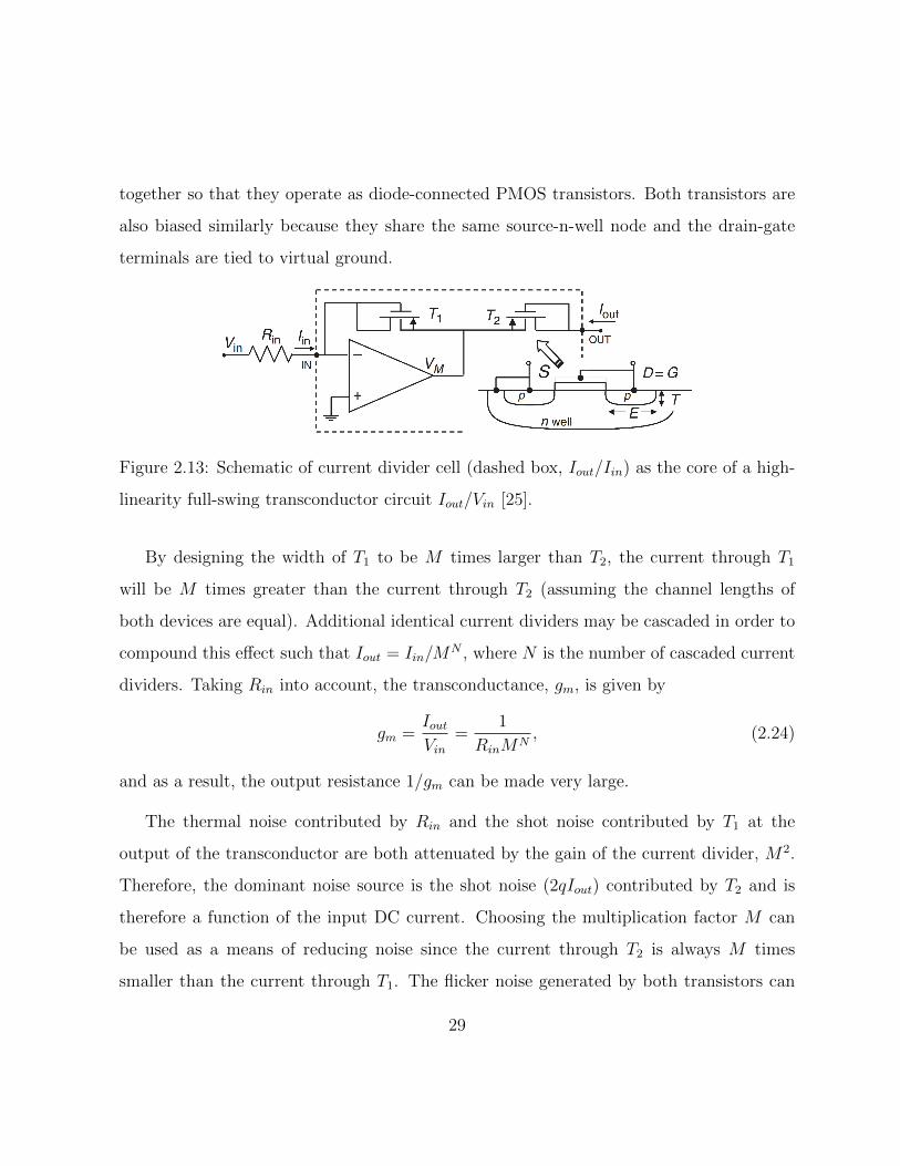
together so that they operate as diode-connected PMOS transistors. Both transistors are
also biased similarly because they share the same source-n-well node and the drain-gate
terminals are tied to virtual ground.
Figure 2.13: Schematic of current divider cell (dashed box, Iout/Iin) as the core of a high-
linearity full-swing transconductor circuit Iout/Vin [25].
By designing the width of T1 to be M times larger than T2, the current through T1
will be M times greater than the current through T2 (assuming the channel lengths of
both devices are equal). Additional identical current dividers may be cascaded in order to
compound this effect such that Iout = Iin/MN , where N is the number of cascaded current
dividers. Taking Rin into account, the transconductance, gm, is given by
gm =IoutVin
=1
RinMN, (2.24)
and as a result, the output resistance 1/gm can be made very large.
The thermal noise contributed by Rin and the shot noise contributed by T1 at the
output of the transconductor are both attenuated by the gain of the current divider, M2.
Therefore, the dominant noise source is the shot noise (2qIout) contributed by T2 and is
therefore a function of the input DC current. Choosing the multiplication factor M can
be used as a means of reducing noise since the current through T2 is always M times
smaller than the current through T1. The flicker noise generated by both transistors can
29

be reduced by maximizing the the total area of the PMOS devices used (large channel
length and width).
2.4.3 Output Voltage Saturation
Node B in the integrator stage of Figure 2.7 is vulnerable to saturation. Assuming the
virtual ground is set to mid-rail, the maximum current that H(s) can process IDCmax is
given by
IDCmax =
∣∣∣∣ VDD
2RDC
∣∣∣∣ . (2.25)
This is unique since IDCmax is not a function of the overall passband gain of the system
(vOUT/iIN = RDCd/Ci).
2.4.4 Noise Performance
As with the analysis of the previous TIAs, the noise of the input op amp Ai is ignored.
The input current noise contributed by the differentiator op amp Ad and resistor Rd is
attenuated by a factor of (Cd/Ci)2 and thus negligible in comparison with the thermal noise
of RDC . Since RDC is implemented using the transconductor discussed in Section 2.4.2,
the input-referred current noise PSD i2n,CARITA(f) due to RDC is given by
i2in,CARTIA(f) = 2qIDCmax , (2.26)
where q is the electronic charge. The current noise generated by an equivalently-sized
linear resistor would be 4kT/RDC . In comparison, the transconductor implementation of
RDC may exhibit reduced noise for low DC currents.
Ignoring the low-frequency attenuation shown in Figure 2.11 and assuming the band-
width is limited by 1/(2πRDCdf ), the RMS input current noise of the CARTIA can then
30

be found using
in,CARTIA =
√qIDCmax
RDCdf
. (2.27)
The SNR of the TIA, in dB, is given by
SNRCARTIA = 10 log10
[iin
2 RDCdf
qIDCmax
]. (2.28)
2.4.5 Design Tradeoffs
The active resistor RDC can be adjusted to set IDCmax for a given application without
affecting the passband transimpedance of the system. This is not so with the TIAs pre-
viously discussed where saturation due to the DC current is always dependent on the DC
gain.
Due to the complexity of the feedback system, each component value must be considered
carefully in order to ensure the system is stable. RDC and the design ofH(s) directly impact
the stability of the system [30]. In order to provide sufficient phase margin in the integrator
stage, RDC should be designed large enough to separate it from the GBP of amplifier Ai
(refer to Figure 2.9).
Implementing RDC as a transconductor makes it possible to achieve the large time
constants required in a CMOS process. The resulting input-referred current noise, however,
is a function of the standing current. The more current that the CARTIA sinks (or sources)
the higher the input-referred current noise. Therefore it is possible that RDC exhibits lower
noise when implemented as a transconductor rather than a linear resistor as long as IDC
is low enough.
31

2.5 Performance Comparison of TIA Architectures
Table 2.1 tabulates the performance of the four TIA architectures discussed in this chapter.
Table 2.1: Summary of performance for various TIA architectures.
Criteria RTIA [1] CTIA [2] RTIA-PI [24] CARTIA [30]
Supply Voltage 3.3 V 3.3 V – 3.3 V
CMOS Process 0.5 µm 0.5 µm discrete 0.35 µm
Transimpedance 25 MΩ 100 MΩ 1.2 GΩ 1.8 GΩ
-3-dB Bandwidth 10 kHz a10 kHz 250 Hz b100 Hz
Input DC Current ±1 nA ±12 nA ±0.4 nA ±25 nA
Range
Input Referred RMS 5 pA 1.35 pA 0.8 pA 0.5 pA
Noise (10 kHz BW)
a Integration time (Tint) is set to 100 µs.
b Bandwidth of the first stage integrator. With the addition of a second stage differentiator,
the bandwidth is extended to 4 MHz while the transimpedance is reduced to 20 MΩ.
32

Chapter 3
Proposed Transimpedance Amplifier
Architecture
This chapter develops a single stage TIA circuit architecture that has sufficient gain to
sense signal currents on the order of tens of pA while maintaining a zero output offset
voltage for DC currents on the order of nA and a noise floor within the fA/√
Hz range.
The proposed TIA also offers continuous-time measurement of input current signals and
an adjustable low-frequency cutoff which is advantageous in several biosensing applications
as discussed in Chapter 1.
3.1 Selecting the Feedback Type
The first step is to determine whether to use a resistive or capacitive feedback architecture
to process the input signal current. In either case, the input DC current can saturate
the circuit and the maximum DC current that the TIA can sink or source is proportional
33

to the DC gain (transimpedance). However, the effect on the resistive feedback is subtly
different from that on the capacitive feedback. Irrespective of the DC current level, the
feedback capacitor Cf must be reset since charge will continuously accumulate until the
output node voltage is saturated. Even for small currents that would otherwise result
in a negligible DC voltage offset in resistive feedback (for an equivalent DC gain), the
capacitive feedback must still be reset eventually. This dependence sets an unnecessary
limit on the measurement time allotted for current measurement (Tint). Moreover, Tint
must be readjusted for every different DC input current level. While it may be trivial to
readjust Tint adjusting Cf is not. Since the gain and bandwidth of the system are also
dependent on Tint and Cf , it is impossible to maintain the same frequency response while
accommodating for different DC input currents. This is not true for resistive feedback
which provides an unlimited measuring time and constant frequency response regardless of
the input DC current level and for this reason, resistive feedback is preferable for current
sensor applications.
The advantages of capacitive feedback are reduced noise and chip area consumption
in comparison with the resistive feedback TIA. In the case of a feedback resistor, these
two aspects must be addressed simultaneously. As shown in Section 2.1.3, input-referred
current noise is inversely proportional to the resistance Rf . Therefore, reducing the noise
comes at the expense of chip area. For the applications discussed in Chapter 1 Rf must be
set to at least 1 GΩ for the TIA to provide sufficient current sensitivity (in the nA range).
The input-referred current noise PSD generated by a 1 GΩ resistor is approximately 4
fA/√
Hz which is satisfactory. However the difficulty lies in implementing such a large
resistance on chip. As a result, the TIA with feedback transconductor in Figure 3.1 is
considered.
A high transimpedance can be achieved using an active transconductor in the feedback
34

Figure 3.1: Transimpedance amplifier with feedback transconductor.
loop of the TIA instead of a single linear resistor. In the same way a conventional TIA
with feedback resistor Rf has an overall transimpedance given by Vout/Iin = −Rf , this TIA
architecture, with active transconductor Gm, provides a feedback resistance Rf = 1/Gm.
3.2 Feedback Transconductor Implementation
The transconductor used in the proposed TIA shown in Figure 3.2 is inspired by [25].
As with previous TIA architectures, the transconductor connects amplifier A1 in negative
feedback which sets a virtual ground at the inverting input. Since the impedance looking
into the inverting input is extremely large, the input current iIN is forced through the
feedback branch and into Gm.
The two-stage transconductor in Figure 3.2 is formed using amplifiers A3 and A4 and
resistors Rb and MRb, where M is a multiplicative factor. Amplifiers A3 and A4 are
connected in negative feedback and drive their respective inverting input node voltages
35

Figure 3.2: Transimpedance amplifier with two-stage feedback transconductor.
towards virtual ground. Therefore, the only node voltages that can vary are Vout, V3 and
V4. In addition, the voltage across each pair of Rb and MRb resistors is the same. As a
result, iIN = i1 flows through the resistor MRb which raises the output voltage of A4 to V4.
Now the voltage across Rb is also V4 and current i2 flows. Currents i1 and i2 can therefore
be expressed as follows:
i1 =−V4MRb
and i2 =−V4Rb
. (3.1)
Equating i1 and i2 yields i2 = Mi1. Note that the that currents i1 and i2 have been defined
in the schematic to flow in opposite directions since this will always be the case. Nodal
analysis is applied to the second stage and gives
i2 =V3MRb
and i3 =V3Rb
, (3.2)
which adds another current gain factor of M since i3 = Mi2. It should be evident at this
point that the node voltages Vout, V3, and V4 may drop below the virtual ground as a result
of the input current which is expected to be bidirectional [29]. Therefore, the voltage rails
36

along with the virtual ground must be chosen in order to accommodate for this. This is
discussed further in Chapter 4.
Aggregating the effect of these two transconductance stages means that Iout = IinM2.
This current gain is used to provide a large 1/Gm such that the overall gain of the TIA is
Vout
Iin
= − 1
Gm
= −M2Ra. (3.3)
Therefore, large gain can be achieved by adjusting the factor M . This transimpedance
can only be obtained as long as the base resistance Rb remains constant over both stages
(and any subsequent stages). It is possible however, to use a different M factor across the
two stages so that Eq. (3.3) becomes 1/Gm = −M1M2Ra where M1 and M2 are the gain
factors for first and second stages of the transconductor respectively.
The fact thatM is effectively the ratio of two resistors is advantageous since the specified
resistance values for Rb and MRb are subject to error due to process variation. Considering
that Ra is obviously subject to the same error, the design strategy used to implement this
TIA is to make M as large as possible by interleaving Rb and MRb while taking more care
with the layout of Ra to ensure negligible error.
In contrast to the transconductor presented in [25], linear resistors are used in the feed-
back transconductor instead of MOS-bipolar pseudo-resistors in order to improve linearity.
In [25], diode-connected PMOS devices with different widths are used in order to obtain
the current division behaviour mentioned above. These PMOS pseudo-resistors contribute
only shot noise and flicker noise which are, in general, much less significant and more eas-
ily remedied than thermal noise as mentioned in Section 2.4.2. For this design linearity is
preferred over noise performance.
It should be noted that resistors implemented in CMOS 0.35 µm technology are not
perfectly linear. Integrated resistors exhibit both voltage and temperature dependencies,
37

the extent of which is determined by the mask layer used. The physical layout of each
individual resistor will also contribute to the linearity of the system. However, similar
dependencies exist for PMOS devices and thus linear resistors are best suited to ensure
system linearity.
3.2.1 Noise Performance
Resistors Rb and MRb contribute thermal noise to the total input-referred current noise
of the TIA. The input-referred current noise PSD i2in(f) contributed by all the resistors in
the transconductor chain is given by
i2in(f) =kT
MRb
[4 +
1
M2+
1
M3+
1
M4
]+
kT
M4Ra
(3.4)
The above equation has three useful design implications. First, the most significant term is
4kT/MRb which is contributed by the MRb resistor in the transconductor that is connected
to the TIA input. Thus MRb should be maximized to reduce the thermal noise. Second,
the multiplication factor M should be maximized to reduce the effect of each noise term
in Eq. (3.4). Finally, the thermal noise generated by Ra is negligible since it is attenuated
by a factor of M4.
3.3 Low-Frequency Input Signal Suppression
The effects of low-frequency input currents are suppressed by zeroing the output DC level
of the TIA using the non-inverting integrator composed of amplifier A2, resistor R2, and
capacitor C2 shown in Figure 3.3 [24]. The low-frequency behaviour of the TIA is estab-
lished by the zero and pole generated by integrator time constant R2C2. In order to aid in
38

the analysis that proceeds low-frequency cutoff, fL is defined as
fL =1
2πR2C2
. (3.5)
This frequency characterizes two modes of operation for the system in Figure 3.3, one mode
for frequencies below fL, and another for frequencies above fL. The TIA gain for input
signals at frequencies near fL is given by
Vout(s)
Iin(s)≈ − 1
GmA20
1 + sR2C2A20
1 + sR2C2
, (3.6)
where A20 is the open-loop DC gain of A2. As demonstrated by the above equation, the
pole and zero are separated by a factor A20 and the TIA gain is attenuated by the same
factor. At input-signal frequencies below fL, the impedance of C2 becomes very large and
behaves as an open circuit. In this way amplifier A2 operates in open-loop and the voltage
gain Vx/Vout is nearly equal to A20 , where Vx is an intermediate node in the TIA feedback
loop as shown in Figure 3.3. Since the current through R2 is zero, the voltage at the
non-inverting input of A2 is grounded (midway between VDD and VSS). As a result, A2
regulates Vout through the overall feedback. Note here that the transimpedance Vx/Iin is
still 1/Gm and is prone to saturation due to DC input current.
Conversely, at input signals at frequencies above fL, the impedance of C2 becomes very
small and behaves as a short circuit. This allows signals to propagate directly to Vout as
A2 operates in a unity-gain configuration at these frequencies. However, A2 successfully
decouples any voltage amplification due to DC current from Vout . Figure 3.3 also illustrates
the parasitic capacitance Cp in parallel with the feedback transconductor which affects the
high-frequency response of the TIA. A reasonable estimate for Cp is on the order of 100 fF.
At frequencies greater than fL, the TIA gain is given by
Vout(s)
Iin(s)≈ − 1
Gm
1
1 + sCp/Gm
, (3.7)
39

Figure 3.3: Transimpedance amplifier architecture with feedback transconductor and inte-
grator to suppress input currents below the low-frequency cutoff.
which shows the high-frequency cutoff of the TIA. Figure 3.4 depicts the expected frequency
response of the TIA.
Figure 3.4: Expected frequency magnitude response of the proposed TIA.
40

3.3.1 Bandwidth Tuning
The low-frequency cutoff of the TIA can be adjusted by modifying the zero and pole
generated by the integrator time constant R2C2. In order filter out the effect of the DC
current on the output fL must be 100 Hz or lower. Using Eq. (3.5), this means that
R2C2 must be on the order of ms or lower. The available technology, CMOS 0.35 µm,
limits resistor values to only tens of MΩ and capacitor values to tens of pF. The solutions
discussed in this section addresses this issue by using alternative implementations of R2 to
achieve high resistances.
First, it is necessary to show that R2 cannot be implemented using the transconductor
outlined in Section 3.2. The reason for this is that the input to the transconductor is set
to ground as shown in Figure 3.5. The voltage across Ra is zero since it is grounded on
one side (VGND = 0) and a virtual ground is regulated by A3 on the other. Consequently,
current i3 must be zero and V4 = VGND. By the same logic i2 = 0 and A3 will either sink
or source the input current i1. Regardless of the input current i1 to the transconductor,
i2 and i3 will remain zero since VGND cannot fluctuate. Therefore, the effective resistance
that the transconductor supplies is that of MRb which is insufficient.
Figure 3.5: Transimpedance amplifier with transconductor feedback and integrator to sup-
press input currents below the low-frequency cutoff.
41

A more practical alternative is to use a PMOS transistor as a pseudo-resistor as shown
in Figure 3.6 where ID is the drain current. This device was mentioned briefly in Section
2.4.2 and will now be analyzed further. The PMOS pseudo-resistor has two modes of
operation defined by the applied VGS. For negative VGS, the device functions as a diode-
connected PMOS transistor. As long as the PMOS operates in the subthreshold regime
(|VGS| < |Vtp|), the relationship between voltage and current is exponential. For positive
VGS, the p-n junction diode formed between the drain and the body is forward biased and
the device is operating as a lateral BJT [32]. In either case, the incremental resistance is
extremely high.
Figure 3.6: Diode-connected PMOS pseudo-resistor, where the gate-drain and source-body
terminals are shorted.
Figure 3.7 shows a transient simulation of ID for a single PMOS pseudo-resistor given a
0.5 V amplitude 1 kHz signal where significant distortion is observed. Large-signal voltages
give rise to variations in VGS on the order of mV. This exceeds the linear region of the diode
IDS vs. VDS curve shown in Figure 3.8(a). Figure 3.8(b) shows the effective resistance of
the diode-connected PMOS pseudo-resistor (dVGS/dIin). Variations on the order of tens
of mV can cause large scale variations in the impedance of the PMOS device.
In order to reduce this distortion, identical devices are connect in series [33]. The
total potential drop across the chain of PMOS devices as a result of the large signal is
42

Figure 3.7: Transient simulation of VGS for PMOS pseudo-resistor shown in Figure 3.6.
equally subdivided across individual devices as shown in Figure 3.9(a). Therefore, with
every additional PMOS, the potential drop across each individual device is reduced and
by extension, the distortion as well.
Although this method does provide sufficient resistance, fL is not well controlled. While
it may be possible to set fL accurately in simulation using these devices, fL will vary due
to process variations. Also, once the transistors are laid out, fL cannot be modified.
Alternatively, the PMOS devices can be configured as shown in Figure 3.9(b) where
the gate terminal of the PMOS devices are shorted together and connected to an I/O pad.
To achieve very high on resistance, the PMOS devices can be operated in the subthreshold
regime. Figure 3.10 shows the IDS vs VDS curve in the 0.35-µm CMOS technology of a
subthreshold PMOS transistor with width and length of 4 µm by 2 µm.
As Vctrl increases the effective resistance will also increase pushing fL to lower frequen-
cies and vice-versa.
43

(a) (b)
Figure 3.8: (a) IDS vs VDS curve in the 0.35-µm CMOS technology of a diode-connected
PMOS transistor with width and length of 4 µm and 2 µm, respectively. Terminal pairs
gate-drain and source-body are shorted. (b) The effective resistance of the diode-connected
PMOS. Calculated by taking the derivative of (a) and inverting (dVGS/dIin). The sharp
drop in resistance at 0 V is a result of the numerical modeling of the simulator.
(a) (b)
Figure 3.9: PMOS devices connected in series to reduce distortion by subdividing applied
voltage equally across all devices operating (a) as diode-connected PMOS/lateral BJT
devices and (b) in the subthreshold regime with an applied control voltage VCTRL.
44

(a) (b)
Figure 3.10: Simulation of (a) the IDS vs. VDS curve and (b) effective resistance under
various control voltages (Vctrl) for a single subthreshold PMOS device.
3.4 Comparison of Proposed TIA with other Archi-
tectures
While the system shown in Figure 3.3 is still subject to saturation at Vx, unlike the classical
resistive feedback TIA, the effects of the input DC current on Vout are suppressed and the
voltage swing is maximized. Also, by implementing a transconductor in the feedback path,
high gain and low noise are achieved. Though capacitive feedback with switching does
have better noise performance, the proposed design is preferable since no constraint exists
on the time allotted for current measurement.
In contrast to the RTIA-PI discussed in Section 2.3, the proposed TIA architecture
is more amenable to CMOS integration since the transconductor outlined in Section 3.2
is used to achieve the desired gain rather then a single linear resistor. Furthermore, the
large time constant invoked by the feedback integrator is controlled and adjustable using
45

subthreshold PMOS devices.
There are two main differences between the proposed design presented above and the
continuous active reset architecture [23] discussed in Section 2.4. First, [23] utilizes two
stages (an integrator and differentiator) while Figure 3.3 can supply sufficient gain in a
single stage. Considering the integrator stage alone, [23] does not provide sufficient gain for
the applications mentioned in Chapter 1. However, this reduced gain in the integrator is
beneficial for sinking or sourcing large input DC currents. Additionally, the integrator alone
is subject to the same bandwidth limitations mentioned in Section 3.3. The differentiator is
required in order to provide the necessary gain and extend the bandwidth. A differentiator
could be added to the output of Figure 3.3, however, the transimpedance between the
input and differentiator output would no longer be 1/Gm. Second, the TIA in Figure 4.1
has an adjustable low-frequency cut off while [23] does not. The ability to manually tune
R2 and adjust the low-frequency cutoff is not available in the implementation of H(s) in
[23].
46

Chapter 4
Circuit Design and Implementation
This chapter discusses the design of the TIA architecture proposed in Chapter 3. The
complete TIA with active resistor for tuning the low-frequency cutoff is shown in Figure 4.1.
This design was implemented using a 3.3-V 0.35-µm CMOS technology. Accordingly, the
positive supply voltage VDD is set to 3.3 V and VSS is 0 V. In order to maximize the
available voltage swing and accommodate bidirectional current flow, the virtual ground
VGND is set to the mid-rail voltage 1.65 V. On-chip voltage buffers (not shown) transmit
the circuit output Vout and intermediate node Vx off chip. Capacitor Cin in Figure 4.1
represents the pad, chip package, and PCB trace parasitics at the input of the TIA.
The overall transfer function of the TIA, H(s) = vOUT (s)/iIN(s), is given by
H(s) =−MRb
[1+M(1+A4(s))
A4(s)
][Ra(1+A3(s))+Rb
RbA3(s)
][1+(1+A2(s))sR2C2(1+sR2C2)A2(s)
]1+
[1+sMRb[Cp(1+A1(s))+Cin]
A1(s)
][1+M(1+A4(s))
A4(s)
][Ra(1+A3(s))+Rb
A3(s)Rb
][1+(1+A2(s))sR2C2(1+sR2C2)A2(s)
] , (4.1)
where R2 is the effective resistance of the subthreshold PMOS devices and A1(s), A2(s),
A3(s), and A4(s) are the open-loop transfer functions of each amplifier in Figure 4.1 re-
47

Figure 4.1: Transimpedance amplifier with transconductor feedback and PI controller to
suppress input currents below the low-frequency cutoff.
spectively. As the gain of each amplifier becomes large, H(s) is given by
H(s) ≈ −M2RasR2C2
[1 + sR2C2][1 + s(M2Ra)Cp], (4.2)
as expected. The desired response in the above equation is achievable only if each amplifier
supplies sufficient open-loop gain. Table 4.1 shows the component values selected for the
TIA in Figure 4.1.
Table 4.1: Summary of performance for various TIA architectures.
Component M Ra Rb MRb C2
Value 150 50 kΩ 10 kΩ 1.5 MΩ 1 pF
48

4.1 Bandwidth Tuning
The low-frequency cutoff fL is tuned by implementing an active resistor comprised of two
identical series PMOS transistors operated in the subthreshold regime. Two devices are
used in order to minimize the signal distortion as discussed in Section 3.3.1. Each PMOS
is sized with width and length of 4 µm and 2 µm, respectively.
The effective resistance of these devices is controlled by adjusting the gate voltage,
Vctrl , supported by an off-chip source. Increasing Vctrl increases the overall resistance of
the PMOS devices. Figure 5.5 shows the simulated variation in fL as the control voltage
of the active resistor changes. With C2 = 10 pF, fL can be varied from less than 1 Hz to
more than 10 kHz.
Figure 4.2: Simulated tuning range of the TIA low-frequency cutoff.
Parallel plate capacitor C2 is implemented using two polysilicon layers available in the
49

CMOS process. A unit-size capacitor of 500 fF with dimensions 26.5 µm × 26.0µm, is
used to implement all capacitors in the TIA. Therefore C2 = 1 pF consumes a total area
of approximately 0.0014 mm2.
4.2 Transconductor Design
In order to obtain a nominal transimpedance of M2Ra = 1 GΩ, the two-stage feedback
transconductor has been designed with M = 150, Rb = 10 kΩ, and Ra = 50 kΩ. These
values were selected in order to reduce the overall input-referred current noise as discussed
in Section 3.2.1. As per Eq. (3.4), the larger Rb the lower the noise. However, the upper
limit for the resistance value of Rb is based on the total area that each resistor in the
transconductor occupies. Having Rb = 10 kΩ means MRb = 1.5 MΩ which occupies signif-
icant area. Using Eq. (3.4), the expected input-referred current noise PSD is approximately
1.1064× 10⁻²⁶ A2/Hz or 1.1052× 10⁻¹³ A/√
Hz.
The CMOS 0.35 µm technology supports several resistor types, each exhibiting a par-
ticular resistivity as well as temperature and voltage dependence. A p+ diffusion resistor
is used for Rb and MRb. Although n-well diffusion resistors provide higher sheet resistance
per unit area than p+ diffusion (1050 Ω/sq vs. 150 Ω/sq), MRb is more area efficient when
implemented in p+ diffusion due to the minimum spacing requirement of at least 3 µm
between adjacent n-wells. Resistor Ra is also implemented using a p+ diffusion resistor.
4.2.1 Resistor Layout
The margin of error associated with the transconductance Gm lies in the precision of Ra
and the factor M and not in the specific resistance values of Rb and MRb. Though process
50

variation will introduce some margin of error in the exact resistance value, as long as Rb
and MRb are affected the same way, the designed value of M will be maintained. However,
any variation in Ra will directly affect Gm. This is taken into consideration when designing
the physical layout of each resistor.
The effect of process variation onM is minimized by interleaving the layouts for resistors
Rb and MRb. Having a unit p+ diffusion 20 kΩ resistor of minimum width, MRb = 1.5 MΩ
is constructed using a series combination of 75 unit resistors while Rb = 10 kΩ is realized
using four parallel pairs of two unit resistors in series ([20 kΩ + 20 kΩ]/4 = 10 kΩ). The
purpose of breaking up Rb into eight unit resistors is so that Rb can be evenly distributed
throughout MRb as shown in in Figure 4.3. The 20 kΩ unit resistor has dimensions 320 µm
Figure 4.3: P+ diffusion resistor layout of Rb interspersed throughout MRb.
× 2.5 µm. Therefore, the chip area consumed by a single Rb-MRb pair, with the necessary
spacing between unit resistors, is 0.082 mm2.
Resistor Ra is implemented using ten unit sized 5 kΩ p+ diffusion resistors connected
in series. This unit resistor has dimensions 482.5 µm × 12.8 µm. The layout area of Ra,
51

with spacing, is approximately 0.065 mm2.
The total chip area of all the resistors used in the transconductor (2 × Rb, 2 ×MRb
and Ra) is approximately 0.23 mm2. In comparison, a single 1 GΩ on-chip linear resistor
would consume an area of around 50 mm2 using p+ diffusion.
4.3 Amplifier Design
A single-ended output folded-cascode architecture with PMOS inputs, shown in Figure 4.4,
is utilized as the input stage for each amplifier in the TIA. The tail current Itail supplies
a drain current of Itail/2 to each of the input PMOS devices while Ibias is used to set the
drain current of the cascode current mirror devices. The high output resistance attainable
by cascoded devices is advantageous in achieving the necessary open-loop voltage gain
in a single stage. The load capacitance at this single high impedance node is usually
sufficient for stability. This is desirable for the overall stability of the feedback TIA which
is dependent on the closed-loop stability of each amplifier. PMOS devices are used at the
input as these generally produce less input-referred flicker noise than NMOS devices for a
given area. The folded-cascode also provides reasonable voltage swing at the output.
Each amplifier is designed such that VGND = 1.65 V lies within the common mode
input range. Transistor aspect ratios are selected to reduce the systematic offset voltage at
the output. Bias voltages are adjusted ensure transistors operate in strong inversion and
to maximize the output voltage swing given by
− VSS + 2Vov < Vout < VDD − |Vt| − 2|Vov|, (4.3)
where Vtp is the threshold voltage of PMOS transistors in the CMOS technology used (
≈-600 mV) and Vov is the overdrive voltage VGS − |Vtp|. The voltage gain of the cascode
52

Figure 4.4: Circuit schematic for general folded-cascode amplifier.
amplifier Av is given by the following simplified expression
Av ≈ gm1[gm2Aro2A(ro2||ro12)]||[gm4Aro4Aro4] (4.4)
where gmx and rox is the small-signal transconductance and output resistance of transistor
Mx, respectively. The output resistance of each transistor is set by the bias and tail currents
applied since ro = 1/(λID), where λ is the channel length modulation parameter. For a
given current aspect ratio, gm1 is a function of the Itail as shown by the following expression
gm =
√2ID
µCoxWL
=
√Itail
µCoxWL
. (4.5)
The remainder of this section will summarize the specifications of each amplifier in
53

the TIA and the design decisions required to meet them. A simulation of the open-
loop frequency response and differential transfer characteristic curve are provided for each
amplifier under the load conditions defined by the TIA architecture. The design of the
output buffer used to drive signals off chip is also discussed.
4.3.1 Design of Amplifier A1
In general A1 must have sufficient gain to drive the transconductor feedback system. This
has implications for the overall transimpedance, bandwidth and stability of the TIA. In
order to determine the specifications for A1 Eq. (4.1) can be approximated as
H(s) ≈ −M2RasR2C2
1 + sR2C2
(1 +
[MRa
Rb
] [1 + sMRb[Cp(1 + A10) + Cin]
A10
])−1
, (4.6)
where A10 is the open-loop DC gain of amplifier A1 and A2(s), A3(s), and A4(s) are
assumed to be large and Cin is the parasitic capacitance at the input of the TIA as shown
in Figure 4.1. From Eq. (4.6) it is evident that Cin forms an additional pole with resistor
MRb. However, this pole can be shifted to very high frequencies if
A10 >>Cin
Cp
(4.7)
where Cp is the parasitic capacitance between the input and output nodes. It is reasonable
to assume that Cin will be on the order of tens of pA and Cp on the order of hundreds of
fA. As a result A1 must be designed with a DC gain of at least 60 dB in order to regulate
the input node at VGND.
Using the assumption made in Eq (4.7) and assuming a single-pole roll-off model where
A1(s) = A10/(1 + s/ω10), Eq. (4.6) becomes,
H(s) ≈ −M2RasR2C2
[1 + sR2C2][1 + s(M2Ra)Cp]
([1 +
MRa
A10Rb
] [1 + s
Cp + Cin
A10ω10Cp
])−1
, (4.8)
54

where A10ω10 is the GBP of amplifier A1. The above equations illustrates two additional
constraints on A1. First, the coefficient [1 + (MRa)/(A10Rb)]−1 attenuates the mid-band
gain of H(s) and, therefore, A10 >> MRa/Rb. Given that M = 150, Ra = 50kΩ, and
Rb = 10kΩ, A10 >> 750 V/V. Having already constrained A10 to a minimum of 60 dB (1000
V/V) this condition is redundant. Second, Eq. (4.8) shows an additional high-frequency
pole f3 = A10ω10Cp/2π(Cp + Cin). As this is the third pole of H(s), the TIA may be
vulnerable to instability. In order to ensure stability, f3 must lie at least three decades
above 1/(2πM2RaCp), at approximately 1.5 MHz. Therefore the minimum specified GBP
of A1 is 10 MHz. The stability of the TIA is discussed further in Section 4.4.
Figure 4.5 shows the schematic diagram for A1 with the corresponding transistor widths.
All transistor channel lengths are 1 µm to reduce short-channel effects. Amplifier A1 is
implemented using two identical folded-cascode amplifiers in cascade, A1a and A1b, each
with a DC gain of 70 dB and GBP of approximately 128 MHz. Therefore, the total DC
gain of A1 is 140 dB while the GBP of A1 only increases slightly to 156 MHz. In this
way, sufficient loop gain is provided to regulate the virtual ground at the TIA input while
ensuring stability of the system.
Bias transistors M11 and M12 are at least twice as wide as any other transistor in the
signal path in order to sink high DC current and push out the 3-dB bandwidth of the open-
loop response. Figure 4.6 and 4.7 show the open-loop frequency response of amplifiers A1a
and A1 respectively. The widths of M1A and M2A are reduced in order to minimize the
capacitance at the high-impedance output node, thereby boosting the 3-dB bandwidth.
Maximizing the voltage swing was not a priority for the design of A1. The non-inverting
integrator at the output of A1 ensures low-frequency input signal suppression and regulates
the output voltage of A1 at mid-rail 1.65 V. The maximum input signal current expected
is 1 nA. With a transimpedance of 1 GΩ, the required voltage swing at the output is only
55

Figure 4.5: Circuit schematic for amplifier A1 with channel widths specified. All transistors
have a channel length of 1 µm.
1 V. A1 supplies an output voltage swing of 1.0 V as shown by the differential voltage
transfer characteristic of amplifier A1 Figure 4.8.
Figure 4.6: Open-loop frequency response of amplifier A1a.
56

Figure 4.7: Open-loop frequency response of amplifier A1.
Figure 4.8: Differential voltage transfer characteristic of amplifier A1.
57

4.3.2 Design of Amplifier A2
Amplifier A2 is the core of the non-inverting integrator in the TIA feedback loop used for
low-frequency input signal suppression. As before, the specifications of A2 can be identified
by re-examining Eq. (4.1). Defining the low-frequency cutoff fL = 1/(2πR2C2), becomes
Eq. (4.1)
H(s) ≈ −M2Ra
A20
1 + sA20/(2πfL)
1 + s/2πfL
1
1 + s(M2Ra)Cp
. (4.9)
where A20 is the open-loop DC gain of amplifier A2 and A1, A3, and A4 are assumed
to be large. As described in Section 3.3, A2 operates in open-loop for frequencies below
fL and in unity feedback at frequencies above fL. Therefore, the attenuation of the DC
currents is directly proportional to the open-loop DC gain of A2 and should be maximized.
Additionally, A2 must also be unity-gain stable with a phase margin (PM) of at least 60
degrees. At the same time, A2 drives the internal node Vx which is prone to saturation.
Therefore, the output voltage swing of A2 controls the amount of DC current that the TIA
can sink or source and must be maximized.
Figure 4.9 shows the schematic for amplifier A2 which consists of three stages: a PMOS
input cascode stage, source follower, and PMOS common-source (CS) amplifier. The source
follower is used to provide a voltage rise between the cascode output and the gate input
of the CS to ensure that this stage operates in saturation. It is sized to reduce the CS
overdrive voltage thereby enhancing the output swing. The CS stage contributes extra
gain and is also sized to drive the resistive load Ra. Transistors M1 and M2 have a width
of 10 µm in order to reduce the capacitance at the output node. By Eq. (4.4) and (4.5),
reducing the widths of input devices M1 and M2 (while keeping ID and Vov constant)
increases gm1 and gm2 and by extension the total voltage gain of the cascode stage.
Miller compensation capacitor Cz is used to separate the poles generated at the output
58

Figure 4.9: Circuit schematic for three-stage amplifier A2 with channel widths specified.
All transistors have a channel length of 2 µm.
of the cascode and CS amplifiers. However, the zero introduced by Cgs8 is moved to lower
frequencies as a result of the parallel addition of Cz. Resistor Rz (implemented using the
p+ diffusion layer) is sized such that Rz = 1/gm8 in order to move the zero to very high
frequencies. Setting Cz = 2.5 pF and Rz = 1.5 kΩ yields a phase margin of 68 degrees.
The DC gain of A2 is 100 dB to ensure the attenuation of DC signals between Vx and
Vout . The amplifier gain is enhanced due to the increased output resistance provided by
2-µm-channel-length devices in the cascode stage. The 3-dB bandwidth of A2 is 56 Hz to
ensure this amplifier remains stable under unity-feedback operation. Figure 4.10 shows the
open-loop frequency response of amplifier A2. The output voltage swing of A2 is 3.03 V as
indicated by Figure 4.11 shows the differential voltage transfer characteristic of amplifier
A2.
59

Figure 4.10: Open-loop frequency response of amplifier A2.
Figure 4.11: Differential voltage transfer characteristic of amplifier A2.
60

4.3.3 Design of Amplifier A3 and A4
The specifications for amplifiers A3 and A4 are not demanding. Analyzing Eq. (4.1) gives
the following conditions
A30 >>Rb
Ra
and A40 >> 1, (4.10)
where A30 and A40 are the open-loop DC gains of A3 and A4 respectively. Given M = 150,
Ra = 50 kΩ, and Rb = 10 kΩ, A30 >> 0.2 and A40 >> 1 which is easily achieved using a
folded cascode.
Amplifiers A3 and A4 have an identical folded-cascode input stage. Amplifier A3 also
includes an output stage to drive Rb. However, A4 does not require an output stage because
it only has to deliver nA-level currents or less. Figures 4.13 and 4.14 show the open-loop
frequency response of amplifiers A3 and A4, respectively. Figures 4.15 and 4.16 show the
differential voltage transfer characteristic of amplifiers A3 and A4, respectively.
Figure 4.12: Circuit schematic for cascode amplifier A3 with output buffer stage. Amplifier
A4 is identical except without the buffer stage composed of M6 and M7. Channel widths
are specified. All transistors have a channel length of 1 µm.
61

Figure 4.13: Open-loop frequency response of amplifier A3.
Figure 4.14: Open-loop frequency response of amplifier A4.
62

Figure 4.15: Differential voltage transfer characteristic of amplifier A3.
Figure 4.16: Differential voltage transfer characteristic of amplifier A4.
4.3.4 Output Buffers
Two identical unity-gain buffers are used to reduce loading effects at Vout and Vx presented
by the I/O pads and other off-chip elements. A standard two-stage op amp, consisting of63
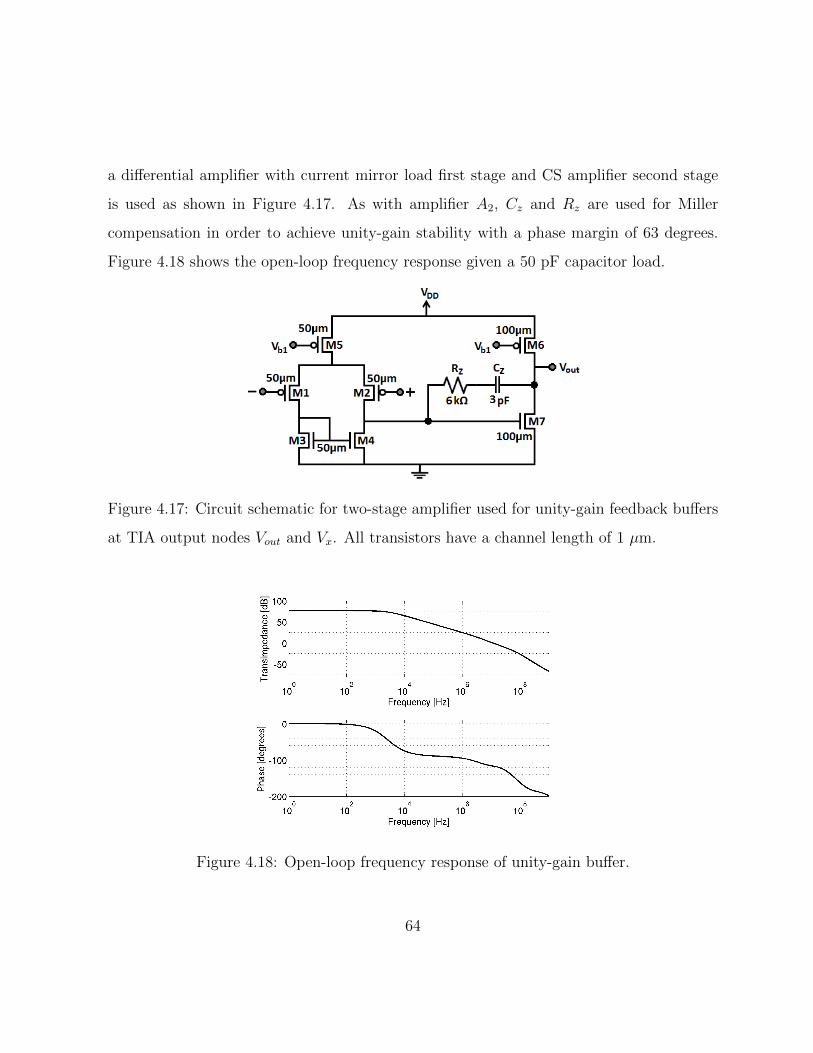
a differential amplifier with current mirror load first stage and CS amplifier second stage
is used as shown in Figure 4.17. As with amplifier A2, Cz and Rz are used for Miller
compensation in order to achieve unity-gain stability with a phase margin of 63 degrees.
Figure 4.18 shows the open-loop frequency response given a 50 pF capacitor load.
Figure 4.17: Circuit schematic for two-stage amplifier used for unity-gain feedback buffers
at TIA output nodes Vout and Vx. All transistors have a channel length of 1 µm.
Figure 4.18: Open-loop frequency response of unity-gain buffer.
64

4.3.5 Bias Circuit
The bias circuit architecture shown in Figure 4.19 is used for amplifiers A1 − A4. A
PMOS current mirror is used since all folded cascodes have a PMOS differential input.
Transistor Mb1 is loaded with two diode-connected NMOS transistors, Mb2 and Mb3,
which provide the bias voltages Vb2 and Vb3. Transistor Mbias and variable off-chip resistor
(potentiometer) Rbias are used to set the current that will be mirrored over to Mb1 and M5
of the associated cascode (or two stage) amplifier to provide the appropriate tail current,
Itail. According to Eqs. (4.4) and (4.5), increasing the tail current increases the ID through
the input PMOS devices and thus increases the transconductance and overall cascode gain.
Figure 4.19: Current mirror circuit used to bias cascode amplifiers A1, A2, A3, and A4
The dotted line between transistors Mbias and Mb1 is used to illustrate the substantial
distance that may exist between their associated gates. Mbias is kept in close proximity
to the pad that will drive Rbias while the physical layout of Mb1 is interleaved with M5 of
the associated amplifier. Metal traces and vias exhibit a sheet resistance and, therefore,
65

the voltage along a long trace may vary as a result of the current that flows. However, this
arrangement of transistors ensures that the voltage set by Rbias at the gate of Mbias is the
same at the gate of Mb1 since the current through the trace connecting the gates is negligi-
ble. If Mbias had been interleaved along with Mb1 where the amplifier is located, and the
trace between the drain of Mbias and Rbias were extended, the voltage difference between
the Rbias pad and the gates of Mbias and Mb1 could be several milli-volts. Transmitting a
the gate voltage rather than the drain current reduces this discrepancy.
The unity-gain buffer amplifiers only require a single bias voltage for the tail current. In
this case, transistors Mb1, Mb2, and Mb3 in Figure 4.19 are not required and only Mbias
and Rbias are used. Table 4.2 specifies the transistor dimensions used for each amplifier.
Table 4.2: Aspect ratio of bias transistors for each amplifier. All dimensions in µm.
Amplifier Mbias Mb1 Mb2 Mb3
A1 100/1 120/1 50/1 100/1
A2 100/2 120/2 50/2 100/2
A3 100/1 120/1 50/1 100/1
A4 100/1 120/1 50/1 100/1
Abuff 100/1 – – –
4.3.6 Summary
Table 4.3 summarizes the simulated performance of each amplifier used in the TIA under
typical process corners.
66
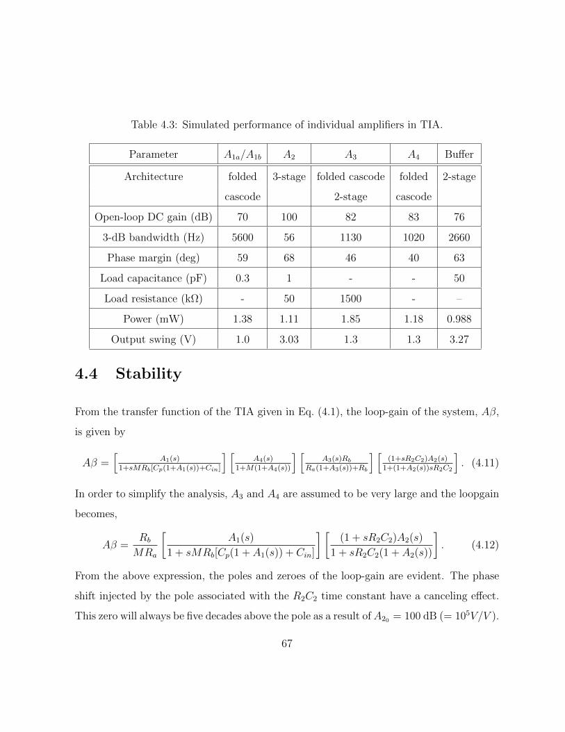
Table 4.3: Simulated performance of individual amplifiers in TIA.
Parameter A1a/A1b A2 A3 A4 Buffer
Architecture folded 3-stage folded cascode folded 2-stage
cascode 2-stage cascode
Open-loop DC gain (dB) 70 100 82 83 76
3-dB bandwidth (Hz) 5600 56 1130 1020 2660
Phase margin (deg) 59 68 46 40 63
Load capacitance (pF) 0.3 1 - - 50
Load resistance (kΩ) - 50 1500 - –
Power (mW) 1.38 1.11 1.85 1.18 0.988
Output swing (V) 1.0 3.03 1.3 1.3 3.27
4.4 Stability
From the transfer function of the TIA given in Eq. (4.1), the loop-gain of the system, Aβ,
is given by
Aβ =[
A1(s)1+sMRb[Cp(1+A1(s))+Cin]
] [A4(s)
1+M(1+A4(s))
] [A3(s)Rb
Ra(1+A3(s))+Rb
] [(1+sR2C2)A2(s)
1+(1+A2(s))sR2C2
]. (4.11)
In order to simplify the analysis, A3 and A4 are assumed to be very large and the loopgain
becomes,
Aβ =Rb
MRa
[A1(s)
1 + sMRb[Cp(1 + A1(s)) + Cin]
] [(1 + sR2C2)A2(s)
1 + sR2C2(1 + A2(s))
]. (4.12)
From the above expression, the poles and zeroes of the loop-gain are evident. The phase
shift injected by the pole associated with the R2C2 time constant have a canceling effect.
This zero will always be five decades above the pole as a result of A20 = 100 dB (= 105V/V ).
67

Figure 4.20 shows the loopgain magnitude and phase of the TIA as R2 is varied using Vctrl.
As Vctrl decreases, R2 decreases, and the pole and zero move to to higher frequencies. The
phase margin is approximately 90O for Vctrl = 1.20V or higher. If Vctrl is decreased to the
extent that 1/(R2C2) ¿ 1/(MRbA10Cp) then the system will become unstable.
4.5 System Simulation
The entire TIA in Figure 4.1, including the buffers (not shown), was simulated in Cadence
Spectre. Figure 4.21 shows the transimpedance magnitude with variable low-frequency
cutoff as set by Vctrl. As Vctrl increases, the low-frequency pole moves closer to zero. Signal
frequencies below the pole set by Vctrl are attenuated by 100 dB, the open-loop gain of A2,
at which point the gain rises at a constant slope of 20 dB/decade. The pass-band gain is
180 dB which is equivalent to a 1 GΩ transimpedance indicating that the effective output
resistance of the transconductor is in fact 1/Gm = M2Ra. We estimate Cp to be on the
order of 100 fF. This leads to a high-frequency cutoff of approximately 1 kHz.
68

(a)
(b)
Figure 4.20: Loop gain magnitude (a) and phase (b) of the system shown in Figure 4.1 for
various values of Vctrl69

Figure 4.21: Transimpedance magnitude of the system shown in Figure 4.1 for various
values of Vctrl.
70

Chapter 5
Experimental Results
The TIA has been implemented in a five-metal, two-poly, 3.3-V 0.35-µm CMOS process.
The fabricated chip is shown in Figure 5.1 where the TIA occupies an area of approximately
0.68 mm2. The input node of the TIA is tied to a pin and the input signal current is supplied
Figure 5.1: Chip photo showing key TIA components.
71

by an off-chip current source to test the chip.
5.1 Test Apparatus
Generating the low currents required to test the proposed TIA is non-trivial given that its
transimpedance is on the order of GΩ. Figure 5.2 shows the circuit schematic of the external
discrete-component current source used to test the TIA. The current source operates by
applying voltage vIN across a large resistor R to generate the test current.
Figure 5.2: Discrete current source used to provide a controllable current to the TIA under
test. A discrete TIA to calibrate current source is also shown.
The transconductance of the current source Itest/Vin can be found by first applying
nodal analysis at V1 and V2 yields,
ItestR[1+A2(s)]R3+R4
A2(s)(R3+R4)=[
A1(s)1+A1(s)
R1
R1+R2− [1+A2(s)]R3+R4
A2(s)(R3+R4)
]Vo + R2
R1+R2Vin . (5.1)
The output voltage node Vo is regulated at virtual ground, VGND by the TIA, which is
buffered by op amp A1 to node V1. If A1 does not supply ample gain, or if Vo is not
72

held precisely at VGND, then some additional current will flow as a result of the Vo term.
Otherwise Eq. (5.1) simplifies to,
Itest
Vin
≈ 1
R
R2
(R1 +R2)R3
[R3 +R4
1 + sω0A20
R3+R4
R3
], (5.2)
where the response of amplifierA2 has been approximated such thatA2(s) = A20/(1+s/ω0),
where A20 is the DC gain of the op amp A2. Eq. (5.3) shows that the bandwidth of the
current source is limited by the GBP of A2. Table 5.1 summarizes the specifications of the
amplifiers used for the current source in Figure 5.2. The low-input bias current of A1 is
highly desirable since Itest is on the order of nA or less.
Table 5.1: Specifications for amplifiers used in discrete current source of Fig 5.2.
A1 A2
Part Number LMP7715MF/NOPB MAX4490AXK+T
Supply Voltage 5.0 V 5.0 V
Gain-Bandwidth Product 17 MHz 10 MHz
Output Voltage Noise PSD 5.8 nV/√
Hz 12 nV/√
Hz
Input Bias Current 100 fA 50 pA
Provided that GBP of A2 is sufficient, the relation of output current to input voltage
is given byIout
Vin
≈ 1
R
R2
R3
R3 +R4
R1 +R2
. (5.3)
By choosing the resistor values appropriately, the input voltage can be attenuated to
supply the desired current to the TIA. Resistors R1−R4 are chosen as 10 kΩ while R = 1
GΩ such that Iout/Vin = 1/R = 1 GΩ. It is necessary for R to be as large as possible
in order to maximize the output resistance of the current source. However, there is a
73

parasitic capacitance Csp associated with R as shown in Figure 5.2 that injects a zero at
1/(2πRCsp). This low-frequency zero makes testing difficult since the zero adds a linear
error to all measurements. In order to characterize this behaviour an on-board TIA made of
discrete components is implemented as shown in Figure 5.2. Figure 5.3 shows the measured
frequency response of the current source when applied to the test TIA. A low-pass filter
(LPF) response is expected, however, due to the zero injected by the current source at
low frequencies the response is irregular. From this it can be shown that the zero lies at
approximately 300 Hz and Csp ≈ 500 fF. Therefore all measurements from the TIA chip
must be post-processed to account for this zero results.
Figure 5.3: Frequency response of the discrete test TIA driven by current source in Fig-
ure 5.2.
74

5.2 Measured Results from TIA Chip
5.2.1 Frequency Response
Figure 5.4 shows the frequency response of the TIA for different Vctrl values. As Vctrl
increases, the resistance of the PMOS active resistor also increases which reduces fL. The
measured passband gain of the system is approximately 1.71 GΩ. This is greater than the
desired 1 GΩ transimpedance due to mismatch between resistors Rb and MRb, as well as
deviation in Ra due to tolerances inherent in the fabrication process. Input current signals
Figure 5.4: Measured transimpedance over frequency with variable low-frequency cutoff.
at frequencies below fL are attenuated at a rate of 20 dB/decade. This decay should
continue steadily to a minimum of approximately 84 dB (the passband gain minus the
open-loop gain of A2). This is not apparent in the measured data since the output signal
drops below the noise floor of the system at very low frequencies. As Vctrl increases from
75

about 0.85 V to 1.2 V, fL decreases from 500 Hz to 0.7 Hz. This variation is in agreement
with the simulated results in Figure 5.5 where the small discrepancies can be attributed
to process variation. The measured high-frequency cutoff of the TIA is approximately
Figure 5.5: Simulated and measured tuning range of the TIA low-frequency cutoff.
650 Hz. With the measured transimpedance of 1.58 GΩ, Cp is estimated to be 150 fF. For
impedance spectroscopy applications requiring higher input signal frequencies, the TIA
bandwidth can be increased by effectively reducing 1/Gm.
5.2.2 Linearity
Figure 5.6 shows the ac output voltage as a function of a 200-Hz input current signal to
illustrate the TIA linearity. At an input current of approximately 0.8 nApp, the output
voltage Vout begins to saturate. This occurs due to the nonlinear behaviour of the active
resistor for large output voltage swings. The slope of the best-fit line to the measured data
76

indicates a transimpedance of approximately 1.79 GΩ before saturation occurs, which is
nearly that measured from the frequency response in Figure 5.4. Figure 5.6 also shows that
the relative linearity error does not exceed 1.1% over an input current range from 0.2 nApp
to 0.8 nApp.
Figure 5.6: Measured relative linearity error of the TIA with an ac input current.
Figure 5.7 shows the measured Vout and Vx for positive and negative dc input currents.
The Vx output follows the current with a constant slope equal to the transimpedance gain
because the low-frequency part of the input signal is not attenuated at this node. The
TIA can process a dc current of ±0.9 nA before Vx saturates at the supply rails. However,
Vout is regulated at the 1.65-V common-mode level over the input current range due to
the low-frequency suppression. The slope of the Vx curve in Figure 5.7 represents the DC
transimpedance of the system.
77

Figure 5.7: TIA output voltage Vout and internal node Vx as a function of dc input current.
5.2.3 Noise
Figure 5.9 shows the PSD of the input-referred current noise of the TIA. The total in-
tegrated noise is 26.7 pArms from 1 Hz to 1 kHz and 27.8 pArms from 1 Hz to 10 kHz.
The thermal noise generated by the feedback transconductor is 10 pArms over a 10 kHz
bandwidth and accounts for a little more than a third of the total input-referred current
noise. The remainder of the noise is likely a result of the flicker noise generated by the
input stages of amplifiers A1 and A2. This is supported by the fact that the majority of
the noise measured lies at low frequencies within the first 1 kHz bandwidth.
78

Figure 5.8: Measured input-referred current noise PSD of the TIA.
5.2.4 Transient Response
Figure 5.9 shows the output voltage transient of the TIA chip as a result of a step input.
A 40 mV input square wave is applied at the input of the discrete current source described
in Section 5.1 to generate a 40 pA step input. As a result of the negative feedback of the
TIA, sharp drops in the input current correspond to large spikes at the output voltage
node. Given enough time the output voltage will settle to virtual ground, at 1.65 V. The
settling time of the system is set as a function of the Vctrl which controls the location of
the low-frequency pole.
79

Figure 5.9: Response of the TIA as a result of a 40 pA step input current. The low-
frequency cutoff of the TIA has been set to 200 Hz.
5.3 Performance Comparison
Table 5.2 tabulates the performance of the work presented in this thesis with that of the
four TIA architectures discussed in Chapter 2.
80

Table 5.2: Summary of performance for various TIA architectures in comparison with the
presented work.
Criteria RTIA [1] CTIA [2] RTIA-PI [24] CARTIA [30] This Work
Supply Voltage 3.3 V 3.3 V – 3.3 V 3.3 V
CMOS Process 0.5 µm 0.5 µm discrete 0.35 µm 0.35 µm
Transimpedance 25 MΩ 100 MΩ 1.2 GΩ 1.8 GΩ 1.71 GΩ
-3-dB Bandwidth 10 kHz a10 kHz 250 Hz b100 Hz 900 Hz
Input DC Current ±1 nA ±12 nA ±0.4 nA ±25 nA ±0.9 nA
Range
Input Referred RMS 5 pA 1.35 pA 0.8 pA 0.5 pA 51.8 pA
Noise (10 kHz BW)
a Integration time (Tint) is set to 100 µs.
b Bandwidth of the first stage integrator. With the addition of a second stage differentiator,
the bandwidth is extended to 4 MHz while the transimpedance is reduced to 20 MΩ.
81

Chapter 6
Conclusion
A CMOS TIA having a measured gain of 1.58 GΩ suitable for low-current electrochemical
biosensors was presented. Use of a feedback transconductor instead of a single linear
resistor to achieve high gain results in chip area savings. The TIA suppresses the effect
of undesirable low frequency input leakage currents on the output. By using an active
resistor in the feedback path, a tunable low-frequency cutoff ranging from 0.7 Hz to 500 Hz
is achieved. A test chip was designed, laid out, and fabricated in a 0.35 µm CMOS process.
6.1 Contributions
The TIA topology introduced in this dissertation is unique in several ways. Unlike the
classical resistive-feedback TIA, the effect of low-frequency currents on the output voltage
is suppressed. Although a capacitive feedback TIAs may provide higher gain for an inte-
grated solution, the TIA presented in this thesis supplies sufficient transimpedance without
limiting the measurement time.
82

The charge-sensitive preamplifier presented in [24] was improved in this thesis by mak-
ing it more amenable to CMOS integration by implementing subthreshold PMOS pseudo-
resistors. These devices enable an adjustable low-frequency cutoff demonstrated in Chap-
ter 4. This additional enhancement also sets this TIA apart from [23]. Though [23] does
provide a larger bandwidth, it makes use of an additional differentiator stage. Taking the
the first stage integrator of [23] alone, the TIA presented in this thesis offers increased
gain, a tunable low-frequency cutoff, and similar bandwidth restrictions.
6.2 Future Work
6.2.1 Additional Transconductor Stages
The advantages of using a transconductor in feedback may be investigated further. It
may be possible to utilize additional transconductor stages in order to further reduce the
chip area required to obtain the necessary transimpedance. In this case the multiplication
factor M may be reduced. However, care must be taken in order to ensure that the overall
feedback of the TIA is negative to avoid issues with stability.
6.2.2 Parasitic Capacitance
Further examination is required in order to identify the parasitic capacitance that con-
tributes to Cp. It may be possible to reduce Cp and thereby increase the overall bandwidth
of the system. However, there will always be a trade-off between gain using the topology
presented in this thesis.
83

6.3 Improvements
Several methods to improve the performance of this TIA were noted during the design pro-
cess. This section will discuss several possible design alternatives that may be incorporated
but were not due to time constraints.
6.3.1 Reduced Noise
Two methods are now described for reducing the overall noise of the TIA. First, the
primary contributor to the input-referred current noise is the thermal noise generated by
resistor MRb as discussed in Section 3.2.1. It may be possible to replace all the MRb and
Rb resistors with subthreshold PMOS devices. The non-linearity of the system may be
mitigated using the methods discussed in Section 3.3.1. Using this technique, the thermal
noise of MRb is replaced by the much lower shot noise of the subthreshold devices.
Second, the input PMOS devices of amplifier A2 in Figure 4.9 are likely contributing
unnecessarily high flicker noise since they are directly connected to the output node of the
TIA. The primary contributors of the flicker noise are the transistors M1 and M2 since they
are 10 mum in width. A2 can thus be redesigned to achieve a lower overall input-referred
current noise by using non-minimal PMOS area for the input devices.
6.3.2 Transimpedance Variation
The precision of the pass-band transimpedance can be improved by addressing the layout
of resistors Ra, MRb and Rb. P-diffusion resistors were favoured in this design because
it accommodated the high resistance and low area restrictions of Rb and MRb. However,
these same restrictions do not apply to Ra which is almost two orders of magnitude less
84

than MRb. An n+ diffusion base resistor is a better choice for Ra as its resistance is less
dependent on the voltage across it as demonstrated by its reduced voltage coefficients in
comparison with the p+ diffusion resistor. As for Rb and MRb, p-diffusion is adequate but
the physical layout of these resistors can be improved in the following way. Although Rb and
MRb are already interleaved to avoid error on M due to process variation, the M generated
by both stages must also match for 1/Gm = M2Ra to hold true. Since each MRb − Rb
transconductor pair is separate, it is possible that the multiplication factor introduced
by the first stage does not match the second. This can be avoided by interleaving both
MRb −Rb pairs within one another.
85

APPENDICES
86

Appendix A
Design of PCB for Testing
Supply and reference voltages are generated off chip using a simple discrete voltage divider
circuit consisting of resistors Rc and Rvar, capacitors Ccer and Ctant, and unity-gain buffer
Abuff as shown in Figure A.1. Resistor Rc remains constant at 10 kΩ while Rvar is a 20 kΩ
potentiometer. By increasing or decreasing Rvar, the output voltage Vn can be increased
or decreased. Ceramic and tantalum capacitors, Ccer and Ctant, are used to filter high
frequency noise from Vn.
Amplifier Abuff is used to avoid loading the voltage divider, to buffer the chip from
undesirable parasitic capacitance, and to supply the necessary bias current for the chip.
An external DC source followed by a low-dropout (LDO) voltage regulator to generate the
5 V rail that is divided down to produce VDD.
A voltage divider similar to that of Figure A.1 is also used to set the control voltage
Vctrl off chip for low-frequency bandwidth tuning. In this case, VDD = 3.3V is divided
down and Rvar is set to 100 kΩ to provide a wide voltage tuning range.
Figure A.2 shows the pin layout of the TIA chip presented in this thesis. The chip was
87

Figure A.1: Discrete voltage divider circuit used to generate off chip voltages.
packaged in the CQFP44A package to be interfaced with the PCB.
Table A.1 maps each of the pins in Figure A.2 to a particular input signal. The package
contains two TIAs with separate bias circuits as well as on additional A1a amplifier for
testing.
Figure A.3 shows the circuit schematic of the test board used for testing the fabricated
chip.
Figure A.4 shows the physical layout of the test board.
88

Figure A.2: Bonding diagram of TIA for CQFP44A package.
89

Table A.1: Mapping table for chip pins.
Pin Number Signal Pin Number Signal
1 – 23 –
2 vb21 24 vb22
3 vb31 25 vb32
4 vb41 26 vb42
5 vbuff1 27 vbuff2
6 avn 28 avp
7 vin1 29 vin2
8 vgnd1 30 vgnd2
9 vout1 31 vout2
10 vnode1 (vx1) 32 vnode2
11 – 33 –
12 – 34 –
13 vsscore1b 35 vsscore2b
14 vsscore1a 36 vsscore2a
15 vddcore1b 37 vddcore2b
16 vddcore1a 38 vddcore2a
17 vssring1 39 vssring2
18 vddring1 40 vddring2
19 vst (vctrl) 41 avout
20 vgnda2 42 vgnda1
21 vb12 43 vb11
22 – 44 –
90

Figure A.3: Test board circuit schematic the fabricated chip.
Figure A.4: Physical layout of PCB for testing the fabricated chip.
91

References
[1] P. Weerakoon, E. Culurciello, K. G. Klemic, and F. J. Sigworth, “An integrated patch-
clamp potentiostat with electrode compensation,” IEEE Transactions on Biomedical
Circuits and Systems, vol. 3, no. 2, pp. 117–125, 2009.
[2] B. Goldstein, D. Kim, J. Xu, T. K. Vanderlick, and E. Culurciello, “CMOS low current
measurement system for biomedical applications,” IEEE Transactions on Biomedical
Circuits and Systems, vol. 6, no. 2, pp. 111–119, 2012.
[3] F. Thei, M. Rossi, M. Bennati, M. Crescentini, F. Lodesani, H. Morgan, and
M. Tartagni, “Parallel recording of single ion channels: a heterogeneous system ap-
proach,” IEEE Transactions on Nanotechnology, vol. 9, no. 3, pp. 295–302, 2010.
[4] J. K. Rosenstein, M. Wanunu, C. A. Merchant, M. Drndic, and K. L. Shepard, “Inte-
grated nanopore sensing platform with sub-microsecond temporal resolution,” Nature
Methods, vol. 9, no. 5, pp. 487–492, 2012.
[5] J. K. Rosenstein, S. Ramakrishnan, J. Roseman, and K. L. Shepard, “Single ion
channel recordings with CMOS-anchored lipid membranes,” Nano Letters, vol. 13,
no. 6, pp. 2682–2686, 2013.
92

[6] P. M. Levine, P. Gong, R. Levicky, and K. L. Shepard, “Active CMOS sensor array for
electrochemical biomolecular detection,” IEEE Journal of Solid-State Circuits, vol. 43,
no. 8, pp. 1859–1871, 2008.
[7] H. Jafari, L. Soleymani, and R. Genov, “16-channel CMOS impedance spectroscopy
DNA analyzer with dual-slope multiplying ADCs,” IEEE Transactions on Biomedical
Circuits and Systems, vol. 6, no. 5, pp. 468–478, 2012.
[8] J. Kew and C. Davies, Ion Channels: From Structure to Function. Oxford, UK:
Oxford University Press, 2010.
[9] B. Hille, Ionic Channels of Excitable Membranes. Sunderland, MA, USA: Sinauer
Associates, Incorporated, 2001.
[10] J. B. Patlak and M. Ortiz, “Two modes of gating during late Na+ channel currents
in frog sartorius muscle,” J. Gen. Physiol., vol. 87, no. 2, pp. 305–326, Feb 1986.
[11] D. Kim, B. Goldstein, W. Tang, F. Sigworth, and E. Culurciello, “Noise analysis and
performance comparison of low current measurement systems for biomedical appli-
cations,” Biomedical Circuits and Systems, IEEE Transactions on, vol. 7, no. 1, pp.
52–62, 2013.
[12] G. I. Marino and B. A. Kotsias, “Cystic fibrosis transmembrane regulator (CFTR) in
human trophoblast BeWo cells and its relation to cell migration,” Placenta, Dec 2013.
[13] S.-Y. Wang, J. Calderon, and G. K. Wang, “Block of Neuronal Na+ Channels by
Antidepressant Duloxetine in a State-dependent Manner,” Anesthesiology, 2010.
93

[14] F. Kirchheim, S. Tinnes, C. A. Haas, M. Stegen, and J. Wolfart, “Regulation of action
potential delays via voltage-gated potassium Kv1.1 channels in dentate granule cells
during hippocampal epilepsy,” Front Cell Neurosci, vol. 7, p. 248, 2013.
[15] A. Brueggemann, M. George, M. Klau, M. Beckler, J. Steindl, J. C. Behrends, and
N. Fertig, “Ion channel drug discovery and research: the automated Nano-Patch-
Clamp technology,” Curr Drug Discov Technol, vol. 1, no. 1, pp. 91–96, Jan 2004.
[16] N. Fertig, A. Tilke, R. H. Blick, J. P. Kotthaus, J. C. Behrends, and G. ten
Bruggencate, “Stable integration of isolated cell membrane patches in a nanomachined
aperture,” Applied Physics Letters, vol. 77, no. 8, p. 1218, 2000. [Online]. Available:
http://link.aip.org/link/APPLAB/v77/i8/p1218/s1&Agg=doi
[17] E. Barsoukov and J. Macdonald, Impedance Spectroscopy: Theory, Experiment, and
Applications. Hoboken, New Jersey, USA: John Wiley & Sons, 2005.
[18] D. Kim, B. Goldstein, W. Tang, F. Sigworth, and E. Culurciello, “Noise analysis and
performance comparison of low current measurement systems for biomedical appli-
cations,” Biomedical Circuits and Systems, IEEE Transactions on, vol. 7, no. 1, pp.
52–62, 2013.
[19] S. Inayat, Y. Zhao, D. Cantrell, D. Dikin, L. Pinto, and J. Troy, “A novel way to go
whole cell in patch-clamp experiments,” Biomedical Engineering, IEEE Transactions
on, vol. 57, no. 11, pp. 2764–2770, 2010.
[20] M. Siksik and V. Krishnamurthy, “An asymmetric approach to modeling ion channels
using finite element analysis,” in Engineering in Medicine and Biology Society, 2009.
EMBC 2009. Annual International Conference of the IEEE, 2009, pp. 3873–3876.
94

[21] C. Krebs, Neuroscience, ser. Lippincott’s Illustrated Reviews Series. Alphen aan den
Rijn, Netherlands: Wolters Kluwer Health, 2011.
[22] G. Wang and W. Dunbar, “An integrated, low noise patch-clamp amplifier for biologi-
cal nanopore applications,” in Engineering in Medicine and Biology Society (EMBC),
2010 Annual International Conference of the IEEE, 2010, pp. 2718–2721.
[23] G. Ferrari, F. Gozzini, A. Molari, and M. Sampietro, “Transimpedance amplifier for
high sensitivity current measurements on nanodevices,” IEEE Journal of Solid-State
Circuits, vol. 44, no. 5, pp. 1609–1616, 2009.
[24] A. Pullia and F. Zocca, “Automatic offset cancellation and time-constant reduction in
charge-sensitive preamplifiers,” IEEE Transactions on Nuclear Science, vol. 57, no. 2,
pp. 732–736, 2010.
[25] F. Gozzini, G. Ferrari, and M. Sampietro, “Linear transconductor with rail-to-rail
input swing for very large time constant applications,” Electronics Letters, vol. 42,
no. 19, pp. 1069–1070, 2006.
[26] B. Leung, VLSI for Wireless Communication. New York, New York, USA: Springer
Publishing, 2011.
[27] D. Johns and K. Martin, Analog integrated circuit design. Hoboken, New Jersey,
USA: John Wiley & Sons, 1997.
[28] C.-A. Gobet and A. Knob, “Noise analysis of switched capacitor networks,” Circuits
and Systems, IEEE Transactions on, vol. 30, no. 1, pp. 37–43, 1983.
[29] I. Axon Instruments, The Axon guide for electrophysiology & biophysics laboratory
techniques. Union City, CA, USA: Axon Instruments, 1993.
95

[30] G. Ferrari and M. Sampietro, “Wide bandwidth transimpedance amplifier for ex-
tremely high sensitivity continuous measurements,” Review of Scientific Instruments,
vol. 78, no. 9, pp. 094 703–094 703–7, 2007.
[31] A. Sedra and K. Smith, Microelectronic Circuits. New York, New York, USA: Oxford
University Press, Incorporated, 2010.
[32] T. Delbruck and C. Mead, “Adaptive photoreceptor with wide dynamic range,” in
Circuits and Systems, 1994. ISCAS ’94., 1994 IEEE International Symposium on,
vol. 4, 1994, pp. 339–342 vol.4.
[33] R. Harrison and C. Charles, “A low-power low-noise cmos amplifier for neural record-
ing applications,” Solid-State Circuits, IEEE Journal of, vol. 38, no. 6, pp. 958–965,
2003.
96