icp etching of silicon - caltechthesis · icp etching of silicon . for micro and nanoscale devices...
TRANSCRIPT

ICP ETCHING OF SILICON
FOR MICRO AND NANOSCALE DEVICES
Thesis by
Michael David Henry
In Partial Fulfillment of the Requirements for the
degree of
Doctor of Philosophy
CALIFORNIA INSTITUTE OF TECHNOLOGY
Pasadena, California
2010
Defended May 19, 2010

ii
2010
Michael David Henry
All Rights Reserved

iii
I would like to dedicate this thesis to multiple people:
Most importantly I dedicate this work to my wife Shaleigh.
I also dedicate this work to the scientists and engineers who have invested much of their time to mentor, teach, and inspire me: Stuart Shacter, Brian Anderson, Axel Scherer, and especially Mike Henry –
my Father.
Finally, I dedicate this work to my sisters Lara, Gina, and Ann.

iv LIST OF PUBLICATIONS
· M.D. Henry, M. Shearn, A. Scherer, Ga Beam Lithography for Nanoscale Silicon
Reactive Ion Etching, Nanotechnology, 21 (2010).
· S. Walavalkar, A. Homyk, M.D. Henry, A. Scherer, Controllable Deformation of Silicon
Nanowires with Strains up to 24%, Physical Review Letters, (2010).
· M.D. Henry, S. Walavalkar, A. Homyk, A. Scherer, Alumina etch masks for fabrication of
high-aspect-ratio silicon micro- and nanopillars, Nanotechnology, 20 (2009).
· Chen, Z. Li, D. Henry, A. Scherer, Optofluidic Circular Grating Distributed Feedback Dye
Laser, Appl. Phys. Lett., (2009).
· M.D. Henry, C. Welch, A. Scherer, Techniques of cryogenic reactive ion etching in silicon
for fabrication of sensors, J. Vac. Sci. Technol. A. (2009).
· Y. Chen, Z. Li, D. Henry, A. Scherer, Optofluidic Circular Grating Distributed Feedback
Dye Laser, CLEO|IQEC Conference Proceeding, (2008).
· G. DeRose, M. Shearn, D. Henry, Y. Chen, A. Scherer, Deep RIE and Cryo-Etching of
Nanostructures in Silicon and Polymers. Microsc. Microanal., S2, 14, (2008).
· B. M. Kayes, M. A. Filler, M. D. Henry, J. R. Maiolo, M. D. Kelzenberg, M. C. Putnam, J.
M. Spurgeon, K. E. Plass, A. Scherer, N. S. Lewis, and H. A. Atwater Radial pn Junction,
Wire Array Solar Cells Conference Record of the Thirty-third IEEE Photovoltaic Specialists
Conference (2008).
· M. Borselli, T.J. Johnson, C.P. Michael, M.D. Henry, O. Painter, Surface encapsulation
for low-loss silicon photonics. Appl. Phys. Lett. , v91 (13), art. no 131117 (2007).

v ·M.D. Henry, A. Homyk, S. Walavalkar, A. Scherer, Selecting the Best Etch Chemistry
and Etch Mask for Achieving Silicon Nanoscale Structures , Oxford News, (2009).
· M. Shearn, X. Sun, M.D. Henry, A.Yariv, A. Scherer, Advanced Plasma Processing:
Etching, Deposition, and Wafer Bonding Techniques for Semiconductor Applications,
Semiconductor Technologies, intechweb.org, (2010).

vi
ACKNOWLEDGEMENTS
I would like to first, gratefully acknowledge the Fannie and John Hertz Foundation for
their generous support for 5 of my years performing research at the California Institute of
Technology. Both the financial support and mentoring received from the Foundation has
been nothing less than spectacular. For this I offer my sincerest gratitude. I would also
like to thank the Robert J. Lang scholarship for a summer of research support.
Scherer Nanofab Research Group: Working for Dr. Axel Scherer and his group has
been one of the highest privileges I have had at Caltech. I have enjoyed learning from him
vacuum technologies, hearing about all the etching stories, and generally learning from
him how to be a balanced and ethical researcher. Kate Finigan has been not only a
fantastic admin, but also a friend. I am indebted to her willingness to help me through
these challenging years. I have closely worked with Andrew Homyk, whom I must say has
greatly impressed me with his knowledge and abilities, and would like to thank him for all
of his help and friendship. Mike Shearn has been one of my closest friends, colleagues,
and my technical diving partner; I have greatly enjoyed working with him and sincerely
hope to continue doing so. I would like to thank Sameer Walavalkar for his collaborating
and friendship over the years. I have always learned from others, including those that
were once my students and are now my peers; thank you Tom Gwinn, Aditya Rajagopal
and Dvin Adalian. I would like to offer my best wishes to them on their future endeavors. I
would also like to extend my gratitude to JQ Huang for her tireless efforts helping me and
correcting my errors.
Professors and Mentors: There are those whom give their most precious commodity,
time, to better others. It is a selfless act which I hope to pay forward. Every now and then

vii they receive a small reward for their efforts; however small this is I hope they receive this
acknowledgment and thanks as such. My most sincerely thanks goes to Tom Tombrello
for always entertaining and encouraging my ideas and directing me forward. I extend my
thanks to Mike Tyszka for his countless work in teaching me NMR and MRI and guiding
my science. Several men at National Semiconductor have spent countless hours teaching
me integrated electronics and design; thank you Stuart Shacter, Greg Smith, and Wade
Leitner. I would like to thank my undergraduate advisor and my very good friend, Brian
Anderson, for introducing physics and quantum mechanics to me. He has spent many
hours teaching and helping me. I am at this point in my education, to a large extent,
because of you.
Caltech Colleagues and Collaborators: Research is no longer the efforts of a single
person; it is now in the realm of the many. I am grateful to this because it has generated
many wonderful friendships and collaborations. I would like to extend my gratitude to Julia
Greer and Andrew Jennings for their efforts and time to teach and work with me
investigating mechanical properties. I hope that our work together continues, mostly
because they are very enjoyable people to work with. I would also like to thank all the
people of the Kavli Nanoscience Institute for all of their efforts and time spent driving my
work forward: Mary Sikora, Guy Derose, Melissa Melendes, and Bophan Chimm. I would
like to particularly thank Nils Asplund. He is the most talented machinist I have ever
encountered and any time I have needed any work done, he immediately has taken care
of it. He has also been a good friend, for that I also thank him.
Friends: Throughout all my successes and failures at Caltech there have always been
the friends whom encourage, support and inspire me. They have always given me their
very best and I hope that I might give them mine. For those that I have already mentioned

viii earlier, you are still in this category. My thanks go to: Raviv Perahia, Tom Johnson, Chris
Michaels, Ryan Briggs, Carrie and Doug Hoffmann, Anna Beck, Andy Downard, Auna
Moser, David Scherer, Chad Weiler, and Uday Khankhoje. I would especially like to thank
my very closest friends whom have been my wingmen in my very best and worst times
and whom I gratefully think of as my greatest friends: Brandon and Matt Blair, Eric Brown,
Matt Eichenfield, and Mike Shearn.
Family: I would like to especially thank those who have stood by me longest. For their
love, understanding and help through the many years, thank you: my wife and very best
friend - Shaleigh Henry, Mike Henry, Carol Price, Lara Sparks, Gina Henry, Ann Hickox,
Shari Henry, Kenny Price, Bill Sparks, Scott Lentine, Brian and Cindy McArdle, Brian
McArdle, Bill and Rae Polkinhorn, Bill and Carla Bergschneider, Anita and Harrison Noe,
Trina Polkinhorn, Ally Polkinhorn, the Whitlows, and the Yosts.
To these people, I humbly offer my most sincere gratitude.

ix ABSTRACT
The physical structuring of silicon is one of the cornerstones of modern
microelectronics and integrated circuits. Typical structuring of silicon requires generating a
plasma to chemically or physically etch silicon. Although many tools have been created to
do this, the most finely honed tool is the Inductively Couple Plasma Reactive Ion Etcher.
This tool has the ability to finesse structures from silicon unachievable on other machines.
Extracting structures such as high aspect ratio silicon nanowires requires more than just
this tool, however. It requires etch masks which can adequately protect the silicon without
interacting with the etching plasma and highly tuned etch chemistry able to protect the
silicon structures during the etching process.
In the work presented here, three highly tuned etches for silicon, and its oxide, will be
described here in detail. The etches presented utilize a type of etch chemistry which
provides passivation while simultaneously etching, thus permitting silicon structures
previously unattainable. To cover the range of applications, one etch is tuned for deep
reactive ion etching of high aspect ratio micro-structures in silicon, while another is tuned
for high aspect ratio nanoscale structures. The third etch described is tuned for creating
structures in silicon dioxide. Following the description of these etches, two etch masks for
silicon will be described. The first mask will detail a highly selective etch mask uniquely
capable of protecting silicon for both etches described while being compatible with
mainstream semiconductor fabrication facilities. This mask is aluminum oxide. The
second mask detailed permits for a completely dry lithography on the micro and
nanoscale, FIB implanted Ga etch masks. The third chapter will describe the fabrication
and in situ electrical testing of silicon nanowires and nanopillars created using the
methods previously described. A unique method for contacting these nanowires is also

x described which has enabled investigation into the world of nanoelectronics. The fourth
and final chapter will detail the design and construction of high magnetic fields and
integrated planar microcoils, work which was enabled by the etching detailed here. This
research was directed towards creation of a portable NMR machine.

xi TABLE OF CONTENTS
List of Publications .................................................................................................... iv
Acknowledgements ................................................................................................... vi
Abstract .................................................................................................................... vii
Table of Contents ................................................................................................... viii
List of Illustrations ..................................................................................................... x
Nomenclature ........................................................................................................ xxii
Preface ...................................................................................................................... 1
Inductively coupled plasma reactive ion etching ...................................................... 3
Overview of Etching ......................................................................................................... 3
Physical Description of Etching ................................................................................. 4
Engineering the Etch ................................................................................................. 9
Cryogenic Silicon Etching .............................................................................................. 14
General Characteristics of Cryogenic Etching ........................................................ 15
SiOxFy Passivation Control ...................................................................................... 19
Aspect Ratio Dependent Etching ............................................................................ 24
Pseudo Bosch Silicon Etching ....................................................................................... 32
General Characteristics of Pseudo Bosch Etching ................................................. 32
Silicon Dioxide Etching .................................................................................................. 38
General Characteristics of the Silicon Dioxide Etch ................................................ 38
Etch Applications ..................................................................................................... 43
Silicon Etch masks .................................................................................................. 47
Etch Mask Requirements ............................................................................................... 47
The Etch Mask Problem .......................................................................................... 47
Undercutting with Metal Masks ................................................................................ 51
Alumina Etch Mask ........................................................................................................ 53
Mask Fabrication Sequence .................................................................................... 55
Alumina Mask Evaluation ........................................................................................ 64
Focused Ion Beam Implanted Gallium Etch Masks ...................................................... 66
Ga Implantation using a FIB .................................................................................... 67
Silicon Etching ......................................................................................................... 70

xii Nanometer Scaled Devices .................................................................................... 86
Vertical Silicon Nanowires ............................................................................................. 86
Alumina Etch Masked Nanowires ............................................................................ 86
Vertical Ga-Silicon Nanopillars ................................................................................ 95
Electrical Properties of Vertical Nanopillars .......................................................... 102
Lateral Ga-Silicon Nanowires / Nanobeams ......................................................... 110
Micrometer Scaled Devices .................................................................................. 121
Components of a Portable NMR Apparatus ................................................................ 121
1 Tesla Magnetic Field and Shimming .................................................................. 121
Copper Planar Microcoils ....................................................................................... 141
Silicon Micropillars Point Schottky Diodes .................................................................. 163
Appendix A – Fabrication Recipes ....................................................................... 173
Resist Patterning .......................................................................................................... 173
Photoresist – Clarion AZ 5214e ............................................................................. 173
Electron beam resist – PMMA 950 A2 .................................................................. 173
Silicon Cleans .............................................................................................................. 174
RCA -1 and BHF Clean Cycle ............................................................................... 174
Etch and Deposition Recipes....................................................................................... 174
Cryogenic Silicon Etch ........................................................................................... 174
Pseudo Bosch Silicon Etch .................................................................................... 175
Silicon Dioxide Etch ............................................................................................... 176
Bosch Silicon Etch ................................................................................................. 176
Appendix B – Conductance of Etch Products from a Trench ............................... 178
Appendix C – Notching Effect in Cryogenic Etching ............................................ 181
Appendix D – Mathematica Code for Microcoil Calculations ............................... 184
Appendix E – Effect of Point Contacts on Resistance.......................................... 185

xiii LIST OF ILLUSTRATIONS
Fig I.1 Isometric (left) and cross-sectional view (right) of an Oxford Instruments
ICPRIE. ................................................................................................................... 6
Fig I.2 Illustration of the ion angular and ion energy distribution functions, with
hypothetical resultant etched profile distortion. Points in IEDF correspond to
different ion kinetic energies, while points in the IADF correspond to different
angles of incidence. ................................................................................................ 9
Fig I.3 Changes in DC bias voltage as ICP power (left) and Fwd power (right) are
increased for the cryogenic silicon etch. .............................................................. 17
Fig I.4 Changes in etch rates as ICP power (left) and Fwd power (right) are increased
for the cryogenic silicon etch. ............................................................................... 18
Fig I.5 Black silicon beginning to form between silicon micropillars. The oxygen flow
rate is too high for the given forward power creating a passivation layer on the
horizontal surface. ................................................................................................. 19
Fig I.6 Demonstration of the effect substrate temperature has on the angle of the
cryogenic etch. The pattern was 20 micron diameter pillars arranged in a
hexagonal array. The etch temperature varied from -130 C down to -122 C. .... 21
Fig I.7 Angle control using O2 flow rate for the cryogenic etch. A linear
correspondence was established for each of the diameter pillars: 5 micron, 10
micron, 20 micron, and 50 micron. ....................................................................... 23
Fig I.8 Cryogenic etch data for various aspect ratios of silicon micropillars. The data
was width normalized to solve for the E and b coefficients. ................................ 27
Fig I.9 Cryogenic etch depth dependence on time for silicon micropillars. The curves
are generated from the solutions to the generalized etching rate equation with
E coefficient set to 1.15 microns per minute and b coefficient set to 0.041. ....... 28
Fig I.10 Cross sectional SEM of a cryogenic etch of 10 micron diameter silicon
micropillars. The etched height was 76.5 microns (aspect ratio of 8.1), masked
with 1.6 microns of AZ 5214e for a selectivity of 89:1. Predicted height was
77.8 microns. Without taking ARDE into account, the predicted height would
be 92 microns. ...................................................................................................... 29

xiv Fig I.11 SEMs of a cryogenic etch of multiple diameter silicon micropillars, etched
approximately 55 microns (left) and 25 microns (right). The outside of the
pillars were predicted to taper inward and a 5 micron gap was expected to
close before the etch depth of 35 microns was achieved. ................................... 31
Fig I.12 Cryogenic etch angle dependence on aspect ratio for silicon micropillars. ......... 31
Fig I.13 Ball and stick models of C4F8 (left) and CF4 (right) molecules. When the
C4F8 molecule ionizes in a plasma, it primarily forms a protective CF2 polymer
chain. Introduction of F ions from an SF6 plasma can neutralize the CF2 into
CF4. Reproduced from www.wikipedia.org. ........................................................ 33
Fig I.14 Changes in DC bias voltage as ICP power (left) and Fwd power (right) are
increased for the pseudo Bosch silicon etch. ....................................................... 35
Fig I.15 Etch depth for various etch times for the pseudo Bosch silicon etch. A linear
least squares fit to the curve yields an etch rate of 284 nm per minute. ............. 35
Fig I.16 Etch rate variation for various ICP powers for the pseudo Bosch silicon etch.
The etches were conducted for 3 minutes and the etch depth averaged over
the sample............................................................................................................. 36
Fig I.17 Etch rate variation for various Fwd powers for the pseudo Bosch silicon etch.
The etches were conducted for 3 minutes and the etch depth averaged over
the sample............................................................................................................. 37
Fig I.18 Etch depth for various etch times for the silicon dioxide etch. A linear least
squares fit to the curve yields an etch rate of 388 nm per minute. ...................... 40
Fig I.19 Etch rate variation for various ICP powers for the silicon dioxide etch. These
etches were conducted for 4 minutes and the etch depth averaged over the
sample. .................................................................................................................. 41
Fig I.20 Two silicon dioxide etches etched under similar conditions except ICP was
3100 W (left) as compared to 1100 W (right) with no significant change in
undercut. This aspect demonstrates the protective nature of the polymer
sidewall passivation. ............................................................................................. 42
Fig I.21 Etch rates for silicon dioxide and silicon etched using the silicon dioxide etch
while varying the oxygen flow rate. Note that no significant change was
noticed but there was an observation of a large amount of oxide grass present
when oxygen was missing. ................................................................................... 43

xv Fig I.22 Cross sectional SEMs of the silicon dioxide grating nanoimprint mold. This
mold was used to create a hybrid PDMS microfluidic dye laser. ......................... 44
Fig I.23 Cross sectional SEMs of the silicon nanowires etched 1.2 microns tall with a 10
nm thermal oxide around the side of the pillars. The silicon dioxide etch was
used to remove the oxide layer from the top of the pillar (the darker circle on
top) and the substrate surface. The left pillar is 100 nm in diameter and the
right pillar is 300 nm in diameter. .......................................................................... 45
Fig I.24 Cross sectional SEMs of planar copper microcoils embedded into an etch
quartz wafer. The silicon dioxide etch was performed for 7.5 microns masked
with chrome. .......................................................................................................... 46
Fig II.1 Loss of photoresist selectivity for the cryogenic etch as oxygen is varied. The
etch conditions were SF6-70sccm, ICP-900W, Fwd-5W, temperature-(-120)C,
and pressure of 10 milliTorr. ................................................................................. 49
Fig II.2 Cross sectional SEM of a pseudo Bosch etch of 30 nm (left) and 100 nm (right)
silicon ridges masked using approximately 55 nm of PMMA. This etch was
terminated before the onset of mask erosion at 256 nm. .................................... 50
Fig II.3 Cross sectional SEM of a cryogenic etch of 10 (left), 20 (middle), and 50 (right)
micron diameter silicon micropillars. The etched height was 30 microns and
was masked with chrome. This etch demonstrates a failure of metal etch
masks not seen with dielectric etch masks. ......................................................... 51
Fig II.4 Cross sectional SEM of a cryogenic etch of 50 (left) and 20 (right) micron
diameter silicon micropillars. The etched height was 37 microns and was
masked with copper. This etch demonstrates a failure of metal etch masks not
seen with dielectric etch masks. ........................................................................... 52
Fig II.5 SEM of 5 micron diameter alumina etch mask on silicon after liftoff. .................. 56
Fig II.6 Cryogenic etch data for various aspect ratios of silicon micropillars. The data
was width normalized to solve for the E and b coefficients. ................................ 57
Fig II.7 Cross sectional SEM of a cryogenic etch of 5 micron diameter silicon
micropillars. The etched height was 83 microns. The alumina mask was
approximately 110 nm thick. ................................................................................. 58

xvi Fig II.8 Cross sectional SEM of a cryogenic etch of 10 (left) and 20 (right) micron
diameter silicon micropillars. The etched height was 103 and 126 microns
respectively. The alumina mask was approximately 110 nm thick. .................... 59
Fig II.9 Cross sectional SEM of a cryogenic etch of 20 micron diameter silicon
micropillars. The etched height was 30 microns. The alumina mask was
approximately 30 nm thick for a selectivity of 1000:1. ......................................... 59
Fig II.10 Cross sectional SEM of a cryogenic etch of 5 (left) and 20 (right) micron
diameter silicon holes. The etched height was 41and 64 microns respectively.
The alumina mask was approximately 20 nm thick. ............................................ 60
Fig II.11 Pseudo Bosch etch data averaged over all the aspect ratios of silicon
nanopillars. ............................................................................................................ 61
Fig II.12 Cross sectional SEM of a pseudo Bosch etch of silicon nanopillars. The pillar
diameters alternated between 40 and 65 nm and were etched 780 nm tall. The
alumina etch mask used was 30 nanometers thick. ............................................ 62
Fig II.13 Demonstration of the difference between a nickel etch mask (left) and alumina
etch mask (right). Cross sectional image of approximately 80 nm diameter
pillars etched to 970 nm (left) and 780 nm (right). The etch conditions were
identical. Note the mask undercut problems of the nickel mask are not present
on the alumina etch mask. .................................................................................... 62
Fig II.14 Bright field reflection microscopy of a 100 nm diameter pillar taken in a FEI
transmission electron microscope. The pillar was etched using the pseudo
Bosch silicon etch and masked using alumina. Note the image is rotated
approximately 60 degrees. ................................................................................... 63
Fig II.15 SEM of alumina masked nanopillar array etched 2.75 microns tall. The
diameters in the array started at approximately 420 nm and cascaded down to
20 nm and then back up to 180 nm. The pillars were etched for 10 minutes
and had 30 nm thick alumina etch mask. ............................................................ 64
Fig II.16 SEM of alumina masked nanowire etched 2.54 microns tall and is 57 nm in
diameter; the etch angle is approximately 90.6 degrees. SEM of alumina
masked silicon nanopillars, with diameters of approximately 50,110,150, 200
nm, etched 2.1 microns tall. .................................................................................. 64

xvii Fig II.17 EDAX measurement of the sputtered alumina film. The peaks are centered
around Oxygen, Aluminum, and Silicon with a ratio of nearly 3:2 of Oxygen to
Aluminum; the same as stoichiometric alumina. .................................................. 65
Fig II.18 Ga+ implantation depth for varying FIB beam voltages as simulated using
TRIM. The etch mask thickness is approximated by 2 times the straggle
length. ................................................................................................................... 69
Fig II.19 Scanning electron micrograph of a dose array for nanoscale SF6/C4F8 etch.
Etch depth was 460 nm with the squares ranging from 500 nm down to 50 nm
in 50 nm increments. Inset is a scanning electron micrograph of Ga implanted
nanoscale dose array in silicon. The large square was where the ion beam
was focused and used as a visual marker. .......................................................... 71
Fig II.20 Ga dose array; the dose required for a given etch depth for the Pseudo Bosch
silicon etch. The diagonal line describes the minimum dose required for
achieving a desired etch depth. Area to the right of the diagonal line, the
dosed structures were successfully masked. Etch mask selectivity is
determined by dividing the etch depth by the Ga mask thickness of 20 nm. ...... 72
Fig II.21 Scanning electron micrograph of a silicon nanopillar, 72 nm in diameter and
800 nm tall. ............................................................................................................ 74
Fig II.22 Scanning electron micrograph of second dose array for nanoscale SF6/C4F8
etch. Etch depth was 448 nm with the squares ranging from 200 nm down to
20 nm in 20 nm increments. ................................................................................. 75
Fig II.23 Scanning electron micrograph of third dose array for nanoscale SF6/C4F8
etch. Etch depth was 448 nm with the pillars ranging from 100 nm down to 10
nm diameters in 10 nm increments. ..................................................................... 76
Fig II.24 Ga dose array; the dose required for a given etch depth for the Cryogenic
silicon etch. The diagonal line describes the minimum dose required for
achieving a desired etch depth. Area to the right of the diagonal line, the
dosed structures were successfully masked. Etch mask selectivity is
determined by dividing the etch depth by the Ga mask thickness of 20 nm. ...... 77
Fig II.25 Scanning electron micrograph of a dose array the cryogenic etch. Etch depth
was 10.1 μm with 5 μm squares. The dose was varied in this array from
1x1016 cm-2 to 5x1016 cm-2 in 0.5x1016 cm-2 increments. .............................. 78

xviii Fig II.26 Scanning Electron Micrograph of Ga masked silicon squares, cryogenically
etched 1 micron tall, to quantify the mask undercut associated with cryogenic
etching. The pattern etched is identical to that used for the pseudo Bosch dose
array. ..................................................................................................................... 79
Fig II.27 Scanning electron micrograph 10 micron diameter silicon pillars, etched 5
microns tall, with an 80 by 20 nm silicon nanowire suspended in between. The
wire is connected 500 nm below the tops of the pillars........................................ 82
Fig II.28 Scanning electron micrograph 5 μm squares with varied doses. When the etch
depth increases over the critical dose depth, the structure begins to etch but
maintains its relative height to its neighbor. ......................................................... 83
Fig II.29 Plot of implanted dose as a function of incident dose, with limiting value is
3*1017 Ga atoms-cm-2. .......................................................................................... 84
Fig III.1 Scanning electron micrograph of a silicon nanowire array, etched 1.5 microns
tall and spatially arranged to allow access for electrical probing. ........................ 88
Fig III.2 Scanning electron micrograph of a 45 nm diameter silicon nanowire, etched
2.5 microns tall, is being electrically probed by a tungsten probe tip and
electrically measured. An interesting observation is the amount of flexing of
the nanowire. ........................................................................................................ 91
Fig III.3 Scanning electron micrograph of a 60, 80, and 100 nm diameter silicon
nanowires, etched 1.5 microns tall spatially arranged to allow access for
electrical probing. .................................................................................................. 91
Fig III.4 Current vs. Voltage measurements of silicon nanopillars; sizes vary from 240
nm to 50 nm in diameter and the lengths are 2.5 microns long. These curves
demonstrate ‘s’ curves with symmetric and non-symmetric behavior. ................ 92
Fig III.5 Current vs. Voltage measurements of silicon nanopillars; sizes vary from 422
nm to 215 nm in diameter and the lengths are 1.5 microns long. Note, the 371
diameter is reduced by a factor of 0.005 for plotting purposes. These curves
demonstrate type 3 curves with symmetric and non-symmetric behavior. .......... 94
Fig III.6 Current vs. Voltage measurements of silicon nanowires; sizes were under 100
nm in diameter and the lengths are 1.5 microns long. ......................................... 95
xix Fig III.7 Scanning electron micrograph of Ga implanted Si nanowires etched 707 nm
tall. The array sizes began at 200 nm and were decreased in 20 nm
increments down to 40 nm. The areal dose applied increases from right to left. 96
Fig III.8 Scanning electron micrograph of Ga implanted Si nanopillars. A tungsten
probe tip makes electrical contact to the top of a 70 nm diameter pillar etched
660 nm tall. ............................................................................................................ 97
Fig III.9 Current vs. Voltage measurements of silicon nanopillars squares masked using
the implanted Ga from the FIB. Sizes were 500 nm stepped down in 50 nm
increments to 150 nm; with the length of 0.615 microns tall. The high currents
seen here demonstrate the improvement the a-Si Ga layer provides for
contacting. ............................................................................................................. 99
Fig III.10 Current density vs. Voltage data from the implanted Ga masked nanopillars.
The pillar heights were 620 nm and the diameters ranged from 220 nm down to
140 nm. Note that the 159 nm and 139 nm current densities are multiplied by
100 for scaling. .................................................................................................... 100
Fig III.11 Current density vs. Voltage data from the implanted Ga masked nanopillars.
The pillar heights were 620 nm and the diameters ranged from 180 nm down to
58 nm. As the diameter decreased, the quadrant I exponential decreased to
very small conduction. ........................................................................................ 100
Fig III.12 Contact resistance for pillars contacted directly by the tungsten probe tip and
for pillars with a a-Si Ga interface between the silicon and tungsten probe. The
black line shows thermionic field emission theory for a 0.7 V barrier height. .... 104
Fig III.13 Illustration of a possible method for the reduction of the contact barrier when
using implanted Ga etch masks. It was observed that the implantation reduces
contact barrier height from 0.7 V to 0.26 V. ....................................................... 106
Fig III.14 Contact resistance for pillars contacted directly by the tungsten probe tip and
for pillars with a-Si Ga interface between the silicon and tungsten probe. The
lines shows thermionic field emission theory for a 0.7 V barrier height (dotted)
and 0.26 V reduced barrier height (solid). .......................................................... 107
Fig III.15 Theoretical saturation current densities, Ja and Jc, reducing as barrier height
increases, as predicted from thermionic field emission theory. The values
used are the same as stated earlier in this section. The forward bias, Ja, is
constantly a smaller than Jb for the same barrier. ............................................. 109

xx Fig III.16 109
Fig III.17 Scanning electron micrograph of Ga implanted Si nanowires 10 microns long
and suspended 3 microns high. The nanowire diameters intended were 75,
50, and 25 nm. Top left shows a 87.5 nm wire, top right and bottom left show a
65.7 nm wire, and bottom right shows a 40.5 nm wire. ..................................... 112
Fig III.18 Scanning electron micrograph of Ga implanted Si nanowires 40 nm in diameter
and 16 microns long. .......................................................................................... 112
Fig III.19 Transmission electron micrograph of Ga implanted Si nanowires 40 nm in
diameter and 10 microns long. ........................................................................... 113
Fig III.20 SEM of 2 tungsten probe tips contacting one of three lateral Ga-Si beams 10
microns long. The I-V measurements of these beam indicates a resistivity
improvement from 40 to ~1 -cm. ...................................................................... 115
Fig III.21 Current vs. Voltage measurements of implanted Ga masked lateral silicon
nanobeams. From the geometry, resistivity of less than 5 Ohm-cm was
inferred. The red curves was for a ~150 nm wide beam, the green curve was
for a ~200 nm wide beam, and the blue curve for a ~250 nm wide beam. ....... 116
Fig III.22 SEM of a lateral implanted Ga masked silicon nanobeam. The beam was
constructed on SOI with a 1 micron thick silicon layer. Note the bright regions
on both the beam and the pad which is interpreted as Ga segregating out of
the etch mask due to a high areal dose. ............................................................ 117
Fig III.23 SEM of a lateral implanted Ga masked silicon nanobeam after a 12 hour
thermal anneal at 1000 C. All of the beams broke under tensile stress (right).
From the chipped region on the pad (left), it is hypothesized that
recrystallization of the silicon occurred and the lack of segregated Ga indicates
that activation occurred. ...................................................................................... 119
Fig III.24 SEMs of a lateral implanted Ga masked silicon nanobeam before (left) and
after (right) a 50 minute thermal anneal at 580 C. Comparison of the two
SEMs indicate that the beam was laterally extended by 10 nm and upon
annealing, the material forcing the extension is pushed to the surface returning
the beam to horizontal. ....................................................................................... 120

xxi Fig IV.1 Demagnetization curves for KJ Magnetics NdFeB magnets of N42 and N52.
The red line is the theoretical demagnetization line; the intersection of the two
lines indicate the magnetic field in the air gap. .................................................. 124
Fig IV.2 Model of the NdFeB magnetic circuit. The blue represents the steel loop and
the brown represents the Garolite holders. ........................................................ 124
Fig IV.3 Picture of the NdFeB magnetic circuit mounted in the apparatus which slowly
brings the magnets together. All of the frame was constructed from non-
ferromagnetic materials. ..................................................................................... 125
Fig IV.4 Comsol simulation for determination of the magnetic field. The pink sections
are contain the magnetic flux, the steel loop and the magnets. The white field
is simulated as free space. ................................................................................. 126
Fig IV.5 Simulation for determination of the magnetic field homogeneity. The top graph
depicts the magnetic field, Bz, plotted radially at the center of the air gap. The
bottom graph shows Bz plotted azimuthally along r=0. ..................................... 127
Fig IV.6 Gaussmeter measurement of the magnetic field homogeneity. The top graph
depicts the magnetic field, Bz, plotted radially at the center of the air gap. The
bottom graph shows Bz plotted azimuthally along r=0. Data points are marked
with an ‘x’. ........................................................................................................... 128
Fig IV.7 Simulation (blue circles) and measurement (red x) of Bz field as the air gap
was increased. The measurement was made using a LakeShore 455
Gaussmeter with the Hall probe mounted on a micrometer. The arrows show
the change in simulations results as the magnets are adjusted from supplier’s
characteristics to the measured Br. .................................................................... 130
Fig IV.8 Simulation of Bz field radial homogeneity as the passive shim diameter is
increased. The susceptibility used was 5000, approximate to that of iron, and
the thickness was 7 microns. .............................................................................. 132
Fig IV.9 Simulation of Bz field radial homogeneity as the passive shim’s susceptibility-
thickness product is increased. The shim diameter used is 25.4 mm or 1 inch.133
Fig IV.10 Effect of combination of 5 shims. The locations and widths were designed to
counter the magnetic field inhomogeneity. ......................................................... 136
Fig IV.11 Effect of adding the shim rings to the collimating lens. The combined effect is a
6 mm diameter range with homogeneity of 50 ppm. These curves were
generated using a finite element magnetics simulator. ...................................... 136

xxii Fig IV.12 SEM of iron shim rings embedded in a silicon substrate (left). A cross sectional
SEM (right) shows the thickness of the layer. The iron was evaporated into
cryogenically etched silicon and the metallization liftoff procedure performed
using the etch mask; this eliminated the need for patterning thick photoresist. 138
Fig IV.13 SEM of iron shim rings embedded in a silicon substrate. By cryogenically
cooling the substrate during evaporation, more than 10 microns of iron was
deposited into the etched silicon. ....................................................................... 139
Fig IV.14 Magnetic field measurements using a Hall Probe mounted on a micrometer
stage. Three conditions were tested, an unshimmed field (black), using one 1
inch diameter Metglas 2605s3a shim (blue), and using two 1 inch diameter
Metglas 2605s3a shims (red). ............................................................................ 140
Fig IV.15 Simulation of Bz field for a 500 micron radius planar microcoil. The simulation
was run at 50 MHz for a 2 turn microcoil. These FEMM simulations allowed for
the signal to noise ratio to be optimized. ............................................................ 144
Fig IV.16 Simulation of the signal to noise ratio for the various microcoils. These FEMM
simulations allowed for the signal to noise ratio to be optimized. ...................... 144
Fig IV.17 Cross sectional SEM of a microcoil ridge separating two trenches where
copper was to be deposited. The cryogenic silicon etch was masked with 1.6
microns of resist. Following the etch, an insulating 1.6 micron thick silicon
dioxide layer was PECVD deposited. ................................................................. 147
Fig IV.18 Deposition rate of low temperature PECVD of Silicon Dioxide. Data was fitted
to a linear deposition rate of 42 nm per minute with an offset of 207 nm. This
data is untested for less than 20 minute deposition times. ................................ 149
Fig IV.19 SEM of the center contact after being mechanically cleaved off and copper
thermally evaporated over the clean P+ silicon. This contact established an
Ohmic tunnel-contact from the copper microcoil to the substrate eliminating the
need for a bridging wire and the required additional fabrication steps. ............. 150
Fig IV.20 Cross sectional SEM of copper wire runs embedded in the etched silicon wafer
and insulated from the substrate using a silicon dioxide CVD layer. ................. 152
Fig IV.21 SEM of silicon planar microcoil with radius of 1000 microns. The center
contact shunts the current to substrate via Ohmic contact. ............................... 153
Fig IV.22 Resistance of a 2 probe measurement of planar microcoils taken using an
Agilent Semiconductor Parameter Analyzer. Measured lead resistance was

xxiii 1.9 Ohms (from probe tip to probe tip). The diagonal line is when the machine
enters current compliance and will not permit the current to increase. The flat
resistance denotes that the copper silicon contact is Ohmic to under 50 mΩ. . 154
Fig IV.23 Magnetic Field measurements along the z-axis for the microcoils using a Hall
probe and Gauss meter. The data, ‘x’, was curve fit using the radius and an
offset from z=0 as the fit parameters to R-square values better than 0.95. The
voltage required for driving the coils at 1 Amp were 2.57, 2.11, 2.42, and 1.64
volts for the large, medium, small, and extra small coils respectively. .............. 156
Fig IV.24 Magnetic Field simulations in FEMM along the z-axis for the microcoils. This
simulation was for a DC current of 1 Amp and shows very good agreement
with measurements. ............................................................................................ 157
Fig IV.25 Top Spice schematic of the large planar microcoil. This model includes the
parasitic capacitances of the coil and contact pad, the coil, lead wires, and
Ohmic contact resistances, and adds matching capacitors C1 and C2 (used to
tune the circuit's resonance). .............................................................................. 160
Fig IV.26 Top Spice simulation of the large planar microcoil. This model includes the
parasitic capacitances of the coil and contact pad, the coil, lead wires, and
Ohmic contact resistances, and adds matching capacitors C1 and C2 (used to
tune the circuits resonance). .............................................................................. 161
Fig IV.27 Reflectance measurement using a Network Analyzer of the microcoil chip
holder. The measured ‘Q’ is approximately 262, with the y-axis in dB. ............ 162
Fig IV.28 Reflectance measurement using a Network Analyzer of the silicon planar
microcoils. The measured ‘Q’s are approximately 22, 5.9, 7.0, and 6.3 for the
extra small, small, medium, and large coils. ...................................................... 162
Fig IV.29 SEM taken in the Quanta as a 10 micron diameter pillar was contacted with a
tungsten probe tip. .............................................................................................. 165
Fig IV.30 I-V measurements of the silicon micropillars etched 25 microns tall. The pillars
were cleaned, mounted in the SEM, and measured identically to that of the
nanopillars. The tungsten probe tip creates a Schottky diode and the backside
contact is Ohmic. ................................................................................................ 167
Fig IV.31 I-V measurements of the silicon micropillars etched 25 microns tall. The
change in barrier height from the ideal height of 0.5 V was removed. .............. 169

xxiv Fig IV.32 I-V simulations of an ideal diode in series with a resistor. The resistor values
were 0 (blue), 0.7 (red), 3.5 (green), 12 (cyan), and 44 (purple) ohms. ............ 170
Fig IV.33 I-V simulations of an ideal diode in series with a resistor modified to account for
the point contact. The resistor values were 0 (blue), 9 (red), 17 (green), 24
(cyan), and 41 (purple) ohms. ............................................................................ 171
Fig A.1 Pressure difference from the between the bottom of the etched channel and
the chamber. ....................................................................................................... 180
Fig A.2 Scanning electron micrographs of 5 micron width silicon ridges. The left image
was a silicon ridge 5.105 microns wide, 530 nm undercut, and etched for 20
min, middle was a silicon ridge 5.018 microns, 1.165 microns, and 40 min, and
the right image was a silicon ridge 5.338 microns, 2.1495 microns, and 60
minutes. ............................................................................................................... 181
Fig A.3 Plot of error factor in resistance (delta R / R) due to contacting the structure
with a point contact. As the aspect ratio gets large, the effect of the contact
diminishes quickly. .............................................................................................. 188

xxv NOMENCLATURE
ICP. Inductively Coupled Plasma
RIE. Reactive Ion Etch
CCP. Capacitively Coupled Plasma
RF. Radio Frequency
IADF. Ion Angular Distribution Function
LN2. Liquid Nitrogen
MFC. Mass Flow Controller
ARDE. Aspect Ratio Dependant Etching
SOI. Silicon on Insulator
SEM. Scanning Electron Microscope
TEM. Transmission Electron Microscope
FIB. Focused Ion Beam
Pseudo Bosch. Term describing a SF6 / C4F8 mixed mode silicon etch
PMMA. Polymethylmethacrylate
CVD. Chemical Vapor Deposition
EDX. Energy Dispersive X-Ray Spectroscopy
SCLI. Space Charge Limited Current
SNR. Signal to Noise Ratio
a-Si. Amorphous Silicon

1 P r e f a c e
Although ultimately this thesis is in partial fulfillment of the requirements for PhD, this
work is also meant for continuity of group knowledge (referred to in the Navy as ‘tribal
knowledge’). The layout of this work is setup to ensure that what I have come to
understand with etching and fabrication are available for the future generations of the
Scherer Nanofabrication Group and users of the Kavli Nanoscience Institute at Caltech.
The basis of the knowledge I have gained has come from installing, repairing, calibrating,
and using four different Inductively Coupled Plasma Reactive Ion Etchers and a Plasma
Enhance Chemical Vapor Deposition tool from Oxford Systems. If others find some use or
value from my work, then I am further rewarded.
Chapter I describes, in a general manner, Inductively Coupled Plasma Reactive Ion
Etching using Oxford Systems Plasma Lab 180 and 380s. Working from this general
description, three etches are detailed: Cryogenic silicon etching, Pseudo Bosch silicon
etching, and Silicon Dioxide etching. Data and measurements are displayed showing
specifics needed for tuning etches over a limited phase space with explanations of how to
qualitatively understand these etches. Chapter II then details a few etch masks we have
come to heavily utilize due to the quality resulting from them. Specifically by using a
sputtered alumina etch mask, high aspect ratio silicon nanowires were achievable; better
than 50:1. By using an ion implanted Ga etch mask, a completely dry lithography
fabrication sequence was achieved to fabricate nanoscale devices. This etch mask also
provided the ability to create very low resistance contacts to the silicon nanowires.
Chapter III details the results of probing the silicon nanowires using a SEM and tungsten
probe tips. Details and techniques are also provided for using this tool for other potential

2 applications. Chapter IV provides details on creating microscale devices. Designs and
measurements are provided for devices such as a homogenous 1 Tesla magnetic field,
high ‘Q’ integrated silicon planar microcoils, and vertical micropillars. In the appendices,
one can find calculations detailing all of the fabrication recipes I have developed and used:
calculations useful for understanding problems associated with ICP etching, code for
calculating magnetic fields from microcoils, and calculations for understanding how
bonding wires act to reduce the expected sheet resistance of planar resistors.

3 C h a p t e r I
Inductively coupled plasma reactive ion etching Plasma etching and processing are an essential component for semiconductor fabrication.
Low pressure plasmas can generate high density ion fluxes for anisotropic etching of a
wide array of materials. These etching systems are routinely employed in industry for
fabrication of integrated circuits and microelectromechanical systems. Further, by
independently controlling both the plasma density and the momentum imparted to the
ions, significant improvements in achievable structures can be attained. For the work
described here inductively coupled plasma reactive ion etchers, ICPRIE, are utilized for
fabrication in silicon and silicon dioxide substrates. In particular, this work used 4 etching
apparatus, 3 differently configured Oxford PlasmaLab System 100 ICPRIE 380’s and a
PlasmaLab System 100 ICPRIE 180. This chapter will describe the basic principles of the
ICPRIE, two optimized etch chemistries for silicon, and an optimized etch recipe for silicon
dioxide.
Overview of Etching Plasma etching has two basic requirements, the generation of ions and then imparting
the ions with momentum to direct them at their target. Once the ions reach their target,
the ions can either mechanically or chemically remove atoms from the substrate. Although
this seems like a simplistic overview, careful examination of how to control these aspects
of etching defines the etching system used and examination of the etching mechanisms
defines the chemistry and required etch mask. First, will be a discussion of plasma
generation and how to impart momentum to ions with an incorporated discussion of the
mechanical system used. This chapter will then move to describe requirements to achieve
anisotropic etches, etch masks typically utilized, and finally the different modes of etching.

4 Physical Description of Etching
To create and sustain a plasma for etching, energy input is required. Generally, this
energy is transferred via coupling of an external electric field to ions located in this field.
Generation of the plasma commences with the collisions of initial ions with gas molecules;
the gas is injected into a vacuum system separated by an anode and cathode. The
collisions are produced as ionized electrons are accelerated between the plates, and
collide with the gas. These collisions impart enough energy to further ionize the gas and
further generate an increasing population of ions and electrons. As the voltage increases,
the creation of ions increases over the loss mechanisms until breakdown occurs. This
event is known as the Townsend Discharge. The voltage, at which this breakdown
occurs, V, is highly dependent on the pressure, P, and physical characteristics of the
anode and cathode, known as Paschen’s Law. Here d is the distance between the two
plates and ‘b’ and ‘a’ are fitting parameters.
𝑉𝑉 =𝑎𝑎 ∗ (𝑃𝑃𝑃𝑃)
𝐿𝐿𝐿𝐿(𝑃𝑃𝑃𝑃) + 𝑏𝑏
Different methods exist to generate plasmas with different characteristics [1]. Most
useful to reactive ion etching, RIE, are those generated by capacitive coupled plasmas,
CCP, inductively coupled plasmas, ICP, or some combination thereof. In a CCP process,
energy is supplied as a voltage between an anode and a cathode plate, but in a time-
varying fashion. Most commonly, a radio frequency (RF) voltage is applied to the plates;
the frequency of operation is a band reserved for industrial use by the Federal
Communications Commission in the United State, 13.56 MHz. In this time-varying electric
field, injected gas is ionized by electrons more efficiently than in a static field. The reason
for efficiency improvement is due to the difference in masses between the electrons and
the ions in the plasma oscillating between the anode and the cathode plates. Massive

5 ions are less mobile and cannot track the rapidly oscillating electric field changes.
Although the ionization region is reduced, alternating electrons get multiple opportunities
to scatter and further ionize the gas. Then, by placing a capacitor between the anode
plate and the RF supply, negative charge accumulates on the plate (typically referred to as
the table). The resulting potential difference between the charge neutral plasma and the
negatively charged plate is called the self-bias Vb. The electric field due to Vb drives the
positive ions in plasma towards the negatively charged table. This is the basis for
traditional RIE.
In an ICP process, the excitation is again using a time-varying RF source, but is
instead delivered inductively, via a coil wrapped around the RIE plasma discharge region,
resulting in a changing magnetic field. This changing magnetic field, through the Maxwell-
Faraday equation, induces an electric field that tends to circulate the plasma in the plane
parallel to the CCP plates. Similarly to a CCP, collisions of the rapidly moving electrons
with the slowly moving ions cause further ionizations. Loss of electrons from the plasma
through the grounded chamber walls tends to create a static voltage, deemed the plasma
voltage Vplasma. This is distinct from the self bias Vb, and will be examined later. Inductive
coupling is generally realized through a large 4 to 5 turn copper coil encircling the plasma
chamber.
Arrangement of the ICP with the RIE creates a very powerful combination. In the
typical geometry, the combination means that one is able to change ion density, and other
plasma parameters, using the ICP without significantly perturbing the incident energy of
the ions which is controlled by the CCP. When etching with these combined sources,
generally speaking, the ICP can then control the number of ions reaching the substrate to

6 chemically etch whereas the CCP controls the momentum of the ions reaching the
substrate to mechanically etch.
Analysis Port
ICPGenerator
CCPGenerator
Cryo Stage(–150°C to 400°C)
Helium Backing
Wafer Clamping
Gas Inlet
Pumping
DarkSpace
Glow Discharge
Analysis Port
ICPGenerator
CCPGenerator
Cryo Stage(–150°C to 400°C)
Helium Backing
Wafer Clamping
Gas Inlet
Pumping
DarkSpace
Glow Discharge
Fig I.1 Isometric (left) and cross-sectional view (right) of an Oxford Instruments ICPRIE.
The experimental results discussed here are realized on Oxford Systems Plasma Lab
100 ICPRIE 380 and 180 systems, which utilize a CCP and an ICP power source, as seen
in Fig. 1. Throughout this text, CCP power will frequently be referred to as the “forward
power” or Fwd power, in order to distinguish it from the ICP power and to emphasize its
role in driving ions toward the substrate’s surface. This dual plasma powering affords the
greatest flexibility in altering plasma characteristics such as ion density and bias voltage
independently of each other. These systems have been extensively studied, particularly
for silicon etching [2].
There are a few important features of ICPRIE plasmas that have an effect on etching.
Most noticeable during operation is the region of glow discharge, where visible light
emission occurs from a cloud of energetic ions and electrons. As the gas particles move
in the plasma, collisions occur transferring energy to bound electrons. When these
electrons return to their ground state, a photon may be emitted. The color of the plasma is
7 characteristic of the excited gas species, because the photon energy is a function of the
electronic structure of the gas molecules and their interactions with surrounding molecules
[3]. This can be a useful diagnostic for incorrect plasma striking conditions or other
adverse changes in your plasma. For example, in a multiple gas recipe, sometimes the
emission looks like only one of the gas species, instead of the average of the colors. This
happens when the other species are not being ionized, and thus will cause the process to
take on a completely different character from a calibrated recipe. A second plasma
condition visibly recognizable is that although the CCP has generated a plasma, the ICP
power might not be increasing the ion density due to large power reflections. The two
conditions are distinguishable by the luminosity of the plasmas, whereas the RIE is dim
and the ICPRIE is bright. This is typically due to improper impedance matching between
the ICP’s power supply and the ICP’s coil.
Impedance matching refers to the optimization process of maximizing the power
delivered from the RF power supply to the plasma. For maximum power transfer from the
RF supply to the plasma, the impedance of the load should be the same as the supply.
Furthermore, the impedance of the plasma varies with changes in the injected gas
species, chamber pressure, and desired ICP and Fwd powers. The matching condition
will change even as the plasma transitions from off, high impedance, to lit, low impedance.
To ensure the matched impedance condition, a network of reactive elements are tuned,
typically two capacitors. As an illustration of matching a simplified schematic will be
detailed here for the ICP coils. Assume a plasma has started and now the capacitors are
beginning to automatically tune to minimize the power reflected back to the supply. The
ICP coil (and plasma) can be modeled as an inductor with a series resistance (s*Lcoil +Rcoil)
which is needed to be matched to a supply’s output resistance, typically 50 Ohms and

8 completely real (Rsupply). To match the load impedance, consisting of both real and
reactive terms, to a real resistance, a capacitive term is placed in parallel with the ICP coil
(s*Lcoil +Rcoil||1/s*C1). The capacitive element, C1, is then tuned to make the real term
equivalent to that of the supply. To tune the reactive part of the load, a second capacitive
element is placed in series with the load, C2. Typical RF supplies are tuned to be strictly
50 or 75 ohms with no reactance, leaving the series capacitor to zero out the reactive
component of the load; equivalently stated as it matches the phase of the load to the
power supply. Since the inductance of the ICP coil is directly proportional to the
susceptibility of the space the induced magnetic field encompasses, changing the
characteristics of the plasma will change the inductance. For this reason, different etch
recipes will have different matching conditions and significant variations in the values of
the matching capacitors can indicate deviations from the desired etch. Matching circuits
are never as simple as stated here; it is commonplace to find inductive elements in the
tuning circuits. However the analysis can be generalized and is still the basis of the
matching circuitry. The first equation below permits solving for C1. The second equation
was found by setting the reactance to zero and is used to solve for C2.
𝑅𝑅𝑠𝑠𝑠𝑠𝑠𝑠𝑠𝑠𝑠𝑠𝑠𝑠 =𝑅𝑅𝑐𝑐𝑐𝑐𝑐𝑐𝑠𝑠
(1 − 𝜔𝜔2𝐿𝐿𝐶𝐶1)2 + 𝜔𝜔2𝑅𝑅𝑐𝑐𝑐𝑐𝑐𝑐𝑠𝑠 2𝐶𝐶12
1𝜔𝜔𝐶𝐶2
= 𝜔𝜔[𝐿𝐿 ∗ (1 −𝜔𝜔2𝐿𝐿𝐶𝐶1) − 𝑅𝑅𝑐𝑐𝑐𝑐𝑐𝑐𝑠𝑠 2𝐶𝐶1](1 − 𝜔𝜔2𝐿𝐿𝐶𝐶1)2 + 𝜔𝜔2𝑅𝑅𝑐𝑐𝑐𝑐𝑐𝑐𝑠𝑠 2𝐶𝐶1
2
Beneath the glow discharge region is a dark space, where atoms are no longer excited
into emitting photons due to the depletion of electrons. This dark space is also the part of
the plasma that most directly affects the paths of incoming ions that will accomplish the
etching. Neutral atoms and other ions will tend to scatter the otherwise straight path of the
ions from the edge of the glow discharge to the cathode.

9
++
IEDFDark Space
Glow Discharge Region
IADF
Fig I.2 Illustration of the ion angular and ion energy distribution functions, with hypothetical
resultant etched profile distortion. Points in IEDF correspond to different ion kinetic energies, while points in the IADF correspond to different angles of incidence.
To characterize this spread in both energy and trajectory into probability distributions,
the ion angular distribution function, IADF, and the ion energy distribution function, IEDF,
are used (Jansen et al., 2009). These distributions, depicted in Fig. 2, describe the
likelihood that an incident ion has a given energy and trajectory. IADF strongly affects the
sidewall profile, as a wider IADF corresponds to a higher flux of ions reaching the
sidewalls. Similarly, the IEDF controls the types of processes the ions can be engaged in
when they reach the surface, including removing passivation species, overcoming
activation energies for chemical reactions, and enhancing sputtering yield. These
processes determine the performance characteristics of the etch, so understanding these
effects and recognizing associated faults are paramount to optimizing a recipe.
Parameters controlling the IADF and IEDF include the bias voltage Vb, the ion density, the
gas composition, and the mean free path (which also depends on the aforementioned
parameters).
Engineering the Etch
So far, the physics and physical characteristics of the ICPRIE have been described
with respect to the plasma and ion characteristics. But engineers are typically more

10 interested in how the etched features change with each of the parameters mentioned.
Unfortunately, etch characteristics change dramatically as the gases and substrates
change. A few generalizations can be made, though, and these can serve as general
guidelines.
Increase in the Fwd power generally increases the bias voltage. Since the Faraday
dark space changes little the static electric field will increase, thereby imparting more
energy to the ions. This increases the milling aspect of an etch for both the substrate and
the mask. A faster deterioration of the mask implies that one cannot etch the substrate as
long. Further, if the etch rate of the substrate is not significantly increased with the
increase in Fwd power, indicating that the chemical etch rate is faster than the milling rate,
then the mask with etch faster for the Fwd power increase while the substrate etch rate is
left relatively unaffected. Hence the selectivity of the mask is reduced. An increase in the
electric field also imparts more velocity in a direction normal to the substrate. This means
that collisions in the dark space will not change the direction of the ions as much, so the
IADF will become narrower.
Increasing the ICP power directly increases the vertical magnetic field through the
plasma. This will dramatically increase the number of electron-gas collisions in the plasma
to create more ions. Since the electrons and ions remain in the charge neutral plasma,
there will be an insignificant amount of bias voltage increase. Since the ion density in the
plasma is increased, there will be more reactive ions being sent to the substrate increasing
the chemical aspect of the etch. This leads to highlighting the most significant advantage
of etching with an ICPRIE, changes in ion density and changes in ion velocity become
decoupled unlike other RIE systems.

11 Chamber pressure is conventionally controlled using a throttle valve and by
changing the flow rate of gas into the chamber. The throttle valve is situated between the
chamber and the mechanical pumping systems used to modulate the vacuum during
etching, typically backed by some combination of turbo, cryogenic, or direct drive vacuum
pump. Automatic controls on the throttle valve will either control chamber pressure, by
sensing the pressure and opening or closing the throttle valve accordingly, or by setting
the valve to a given position. Gas flow rate is usually established for a given chamber size
to hold a desired pressure. What is more important is the ratio of flow rates if multiple
gases are utilized. Correctly setting the ratio can enable a chosen chemistry to dominate.
In general, addition of more gas will alter the generation rate of ions but the effect is
usually insignificant to ICP power modifications. Controlling the pressure together, the
throttle valve and gas flow do have a significant effects on etched features. In general, in
order to strike a plasma the pressure needs to be set for the gas based on a modified
Paschen’s Law, and this may or may not be the pressure at which the etch is conducted.
Further, once the etch is struck, modification of the etch pressure can change the electric
field. Decreasing the pressure increases the distance for Debye length of the ions in the
plasma, allowing for the plasma to spread; this reduces the dark space which in turn
increases the electric field driving the ions. Further, collisions in the dark space are
reduced which in turn reduces the IADF. Hence a lower pressure can reduce the undercut
seen on the sidewalls.
Although changing the physical parameters of the etch using power and pressure has
a significant amount of control over profile, the most essential aspect of the etch is the gas
chemistry used. Etch chemistries vary widely, even for the same substrate [4]. Here the
focus will be on silicon and silicon dioxide; several etch chemistries will be discussed.

12 Etch chemistries can be generalized into two basic groups, unpassivated and
passivated. Unpassivated etch chemistries are easiest to control, such as with sulfur-
hexafluoride (SF6) or the combination of tetrafluoromethane (CF4) mixed with oxygen (O2).
With the SF6 chemistry, the ICP controls the density of F ions in the plasma and the Fwd
Power controls the momentum applied. Three basic etching mechanisms for the Si exist
under this chemistry: 1) F ions reach the substrate, chemically combine with the Si to form
a volatile SiF4 and are pumped away (chemical etching), 2) F ions impinge on the
substrate and knock away a Si ion (milling or mechanical etching), and 3) F ions impinge
on the substrate, chemically bind with the Si (ion assisted etching). Using the generalities
from earlier, the ICP predominately controls the chemical etch rate, the Fwd Power
predominately controls the milling rate and the IADF, and the pressure controls the IADF.
Changing ratios of different gases can add another parameter to control separate from
those already mentioned, such as with the combination of CF4 and O2. By increasing the
O2 for a given CF4, the etch rate of silicon can be suppressed while the etch rate of silicon
dioxide, slower than that of silicon for low oxygen levels, can be left unaffected. Gottlieb et
al. [5] demonstrated that although the silicon etch rate peaks when the CF4/O2 ratio
reaches 12%, by continually increasing the ratio past 23% silicon etch rate can be reduced
below the etch rate of the silicon dioxide. This idea is intriguing since it adds a new
parameter to control for etching. The biggest disadvantage of unpassivated silicon etches
is that there does not exist any means to protect the etched sidewalls from non-vertical
ions. While increasing the Fwd power and decreasing the pressure can narrow the IADF,
there will always be some ions that will laterally etch the silicon sidewalls. When this
lateral etching becomes an issue passivated silicon etch chemistries are utilized, such as
with nanoscale etching
13 Passivated silicon etches are designed to protect the etched sidewalls from this
lateral etching. Just as a second gas, O2, was used to modify the etch rates of silicon and
silicon dioxide in the CF4/O2 etch, other gases can be used to create passivation layers.
Further, the timing of when the passivation gas is used can be changed as well. This idea
leads to a useful categorization of etches suggested by Jansen et al [2] and will be used
here, pulsed mode and mixed mode silicon etches. Both etch schemes employ forms of
etching combined with passivation that actively protect sidewalls during etching and
improve anisotropy. Each has their own advantages and disadvantages which will
become clear during the discussion. The pulsed mode etch, sometimes referred to as a
chopping etch, uses gas “chopping” to alternately etch and deposit inhibitor on the sidewall
surface. The mixed mode etch uses a gas chemistry to form passivating compounds at the
sidewalls at the same time as etching.
As mentioned, the chopping etch requires two alternating plasma steps. The first step
etches the silicon for a short period then rapidly shuts off the gas and plasma. The second
step then initiates a plasma that deposits an inhibitor film on exposed surfaces. This
alternating sequence continues as the etch progresses in depth. Inherent in the
discreteness of the etching is notching on the sidewalls that occurs every step. The duty
cycle between steps controls the etch angle and the total length of the combined steps
controls the depth of the notching. In contrast, mixed mode etching combines the discrete
etch and passivation steps into a single continuous etch. As the etching gas is driven
down to the substrate, the passivation gas is also directed downward and creates a
protective layer. The passivation rate is selected such that the milling rate for the vertically
directed ions is enough to etch through the horizontal passivation layers and continue
etching into the substrate. When the laterally directed ion etch rate, as determined by the

14 IADF, is less than the horizontal passivation rate, the sidewalls develop a protective
layer. By balancing the ratio of etch and passivation gases for both the pulsed and mixed
mode etches, not only can undercutting be reduced but the angle at which the silicon is
etched can also be controlled.
In this work, multiple passivated etch chemistries are used for silicon etching. The
majority of the silicon etching relies on SF6 etch gas. Described earlier, the F ions and
radicals interact with silicon to generate the etch product SiF4. For passivation gases, O2
and Octafluorocyclobutane (C4F8) are utilized here. The first chemistry discussed involves
using SF6 and O2 at cryogenic temperatures, known as the Cryogenic silicon etch. For
this mixed mode etch chemistry, a reduction in temperature below -85 C permits a SiOxFy
to grow on the sidewalls to act as a passivation layer while the F etches the silicon. A
second mixed mode silicon etch described here uses a SF6 etch gas while simultaneously
passivation with C4F8 [6]. This etch is referred to here as pseudo Bosch; this name refers
to the fact that the Bosch etch utilizes same gas chemistry but in pulsed mode. A
passivated etch chemistry is also demonstrated here for silicon dioxide. This etch
chemistry is similar to the CF4/O2 described earlier, but using C4F8/O2 instead. The
interesting aspect of this etch is that the same gas which creates the passivation is also
the same gas that is etching the silicon dioxide.
Cryogenic Silicon Etching The first etch discussed here is a mixed-mode silicon etch performed with substrate
temperatures ranging from -85 C to -140 C. The cooler wafer temperature encourages
growth reactions of silicon with oxygen to generate thin passivation layers while
simultaneously etching. This section on the Cryogenic silicon etch will detail the

15 characteristics of the etch, etch rate control, angle control, and the notching effects
seen at the top of the etched structures. Finally, techniques are demonstrated for where
this etch is most useful and coupled with a discussion of the appropriateness of specific
etch masks.
General Characteristics of Cryogenic Etching
The cryogenic silicon etch is a passivated etch utilizing SF6 as the etch gas and O2 as
a catalyst for the passivation and was first demonstrated by Tachi et al [7]. As described
earlier, the SF6 is ionized in the plasma to create a mixture of SFx and F species; where x
denotes a number between 1 and 5. The most useful ion from this splitting is the fluorine
ion. When the F ion reaches the substrate, the F can remove a Si atom using one of the 3
etch mechanisms described earlier. When the ions chemically recombine with the silicon
a volatile gas is created, SiF4, and the etch product is pumped from the chamber. What is
specifically unique about this etch is that a passivation layer can be created with O ions
and the partially etch product SiFx. By lowering the temperature below -85 C,
recombination of Si, O, and F becomes energetically favorable and a thin SiOxFy layer is
created [8]. Essentially, as one or two F atoms diffuse into the Si lattice, O atoms can
arrive and bond, Mellhaoui et al [9]. This thin film acts as a thin protection layer from
milling ions such as SF5. If the flux of milling ions is low, for example on the sidewall of the
etched structure, then the passivation can reduce the chemical etching and improve the
anisotropic nature of the etch. It should be noted that the passivation can be created from
other means, such as ionization of the etch gas SiF4. In fact, it has been demonstrated
that injection of SiF4 and O2 can actively passivate during the etch; chopping-mode etches
using this chemistry have also been demonstrated [10]. Upon bringing the wafer back up
to room temperature, this passivation layer then becomes volatile and evaporates away.
16 This passivation scheme becomes very attractive for deep reactive ion etching,
DRIE. Using the mixed-mode scheme, the plasma density and chemical etch rate can be
significantly increased while protecting the sidewalls of the etched structure. Upon
warming the substrate up, the etch mask evaporates. Further, the gases required for the
etch are substantially cleaner and less costly than that required for chopping-Bosch
etching. Since the etching and passivation are continuous, the sidewalls of the etch are
significantly smoother than possible with the chopping-Bosch due to its scalloping etch
characteristics [11]. Indeed, this etch chemistry has generated much interest due to all of
its positive attributes. In particular, two influential papers by de Boer and Jensen et al
[2,12] provide a significant amount of discussion on control over the cryogenic etch. To
assist the reader with developing intuitions with regards to this etch, a qualitative
description of etch control will be discussed here.
It is useful to understand how essential parameters may affect the etching rate and
profile of the etched structure. As stated earlier, the advantage of using an ICPRIE is the
separation of control over the chemical etch rate and milling etch rate. The cryogenic etch
is predominately a chemical etch, so controlling the F ion density greatly controls the etch
rate. Control mechanisms over the ion density include ICP power, SF6 flow rate into the
etcher, and pressure control. Increasing the ICP power essentially ionizes more of the SF6
injected into the chamber. As the ICP power increases, an increase in etch rate is noted
with etch rates recorded from 1 to 10 microns per minute. This increase is easily
attributed to the improvement of the ionization efficiency of the gas. In the same manner,
increasing the injected gas also increases the amount of ionization. Unlike increasing the
ICP power, however, increasing the flow rate of the gas past a critical point for a given ICP
power can lead to a decrease in etch rate, possibly due to an increase in scattering of

17 ions. Although increasing pressure does permit a slight increase in etch rate, significant
pressure increases without increasing the SF6 flow rate can lead to instabilities in the
plasma and difficulty in striking the plasma.
As just stated, the cryogenic etch is predominantly a chemical etch. It was also stated
that DC bias gives a measure of the amount of milling occurring and that Fwd power
generally dominates the DC bias. Evidence for this fact is seen from varying the ICP and
Fwd power. From the data displayed, although ICP power is varied over a range 100
times as big as the Fwd power, it only has 1/5th the effect on DC bias. However, the data
also clearly shows that the overall etch rate is dominated by the ICP power.
Fig I.3 Changes in DC bias voltage as ICP power (left) and Fwd power (right) are increased
for the cryogenic silicon etch.
Increase in the Fwd power, around the 0 to 40 W range, results in almost
immeasurable etch rate changes, although it does offer significant increase in DC bias
voltage. Conversely, increasing the ICP power shows relatively little change in DC bias
voltage but significant increase in etch rate. Clearly, the cryogenic etch is predominantly
more of a chemical etch than a milling etch.

18
Fig I.4 Changes in etch rates as ICP power (left) and Fwd power (right) are increased for the
cryogenic silicon etch.
The starting etch conditions for the measurements made here are as follows:
SF6 70 sccm ICP Power 900 W
O2 5 sccm Fwd Power 5 W
Temperature -120C Pressure 10 mt
As seen, the cryogenic etch is usually performed under very low DC bias conditions.
This demonstrates the significant advantage of low Fwd power etching; if the milling rate is
low, then the etch mask can survive for much deeper etches. For this reason, the
cryogenic etch has been measured to achieve etch mask selectivity values of 100:1 for
photoresist etch masks, 200:1 for silicon dioxide etch masks, and more recently 3000:1 for
alumina. Etch masks and mask selectivity will be discussed in more detail later. From the
selectivity standpoint, one finds that lowering the Fwd power generally increases the etch
mask selectivity. Some amount of milling is required, however. Injection of O2 into the
etcher provided the needed chemistry for passivation. This passivation is highly desired
on the sidewalls for protection, but on the horizontal surfaces the passivation layer needs
to be milled away for the silicon etching to occur. If the Fwd power is too low for a given

19 O2 flow rate at a given temperature, incomplete removal of the passivation on exposed
horizontal silicon surfaces can occur and black silicon can initiate. Black silicon is
essentially silicon spikes that occur due to micro-masking [12]. Presumably, the name
stems from the observation that these spikes appear optically absorbing, flat black. If
black silicon begins for a given etch condition, increasing the Fwd power a few watts can
remove the effect. There is also an aspect ratio dependence on when black silicon occurs
which will be discussed later.
Fig I.5 Black silicon beginning to form between silicon micropillars. The oxygen flow rate is
too high for the given forward power creating a passivation layer on the horizontal surface.
SiOxFy Passivation Control
Passivation control is had using both the temperature and O2 flow. Essentially,
increasing passivation requires improvement in reaction probability; several examples are

20 reducing temperature, requiring more O ions to reach the silicon sidewalls, or
increasing O2 flow rate. Substrate temperatures are automatically controlled by throttling
LN2 to the plate. Typically, lowering the temperature improves the passivation with typical
temperatures in the range of -110 C to -140 C. Holding temperature stable can be critical
as seen from wavy etch sidewall profiles generated as the plate temperature fluctuates by
10 degrees. This effect was demonstrated by the following etch performed under these
conditions:
SF6/O2 70 / 4 sccm ICP Power 900 W
Time 30 Fwd Power 2 W
Temperature -130C Pressure 10 mt
During this 30 minute etch, the temperature dropped to -122 C then cooled back to
-130 C. Qualitatively, as the etch became warmer less sidewall passivation occurred
forcing the etch to become slightly reentrant. As the etch began to slowly cool back to -
130 C the etching angle returned to the optimized 90 degrees. The pattern was
hexagonally spaced pillars of 20 micron diameters separated by 20 microns. The mask
used was AZ 5214e photoresist 1.6 microns thick.
Typically then, it is advantageous to hold the table temperature as steady as possible.
To assist the LN2 regulator on the Oxford machine, the LN2 dewer was pressurized to 35
psi using house nitrogen and regulated. This example is useful in that it clearly shows that
temperature controls passivation.

21
Fig I.6 Demonstration of the effect substrate temperature has on the angle of the cryogenic
etch. The pattern was 20 micron diameter pillars arranged in a hexagonal array. The etch temperature varied from -130 C down to -122 C.
A second method for controlling passivation, and hence etch angle, is the Oxygen
flow rate. Flow rates of O2 typically range from 2 to 10 sccm and can change the angle of
the etch around 10 degrees. The range is based on two extremes, no passivation and the
beginning of black silicon. In the first case, too little oxygen implies that the SiOxFy layer
will not have enough atoms to act as a protective layer. Further, controlling the flow rate in
these low flow regimes becomes difficult based upon the size of the Oxygen mass flow
controller, MFC. The Oxford machines used had 100 sccm Oxygen MFCs which implies
that flows below 2 sccm were unstable. In the second case, so much O2 is present that,
for a given milling rate, small islands of passivation begin to form on the horizontal
surfaces. These stochastically located passivation areas then begin to act as masking for
the silicon and the black silicon forms. For the -120 C cryogenic etching temperatures, it
22 was experimentally determined that for low aspect ratio trenches the maximum O2 flow
rate was 7.5 sccm when Fwd power was set to 5 W.
Controlling O2, then, provides a useful mechanism for controlling the angle of the
silicon etch. This work has be detailed elsewhere [13] and the results will be summarized
here. To determine the angle, silicon micropillars were etched with different O2 flow rates.
The mask used was 1.6 microns of AZ 5214e of photoresist. The pattern utilized was 5
micron circles separated by 5 microns, 10 micron circles separated by 10 microns, 20
micron circles separated by 20 microns and 50 micron circles separated by 50 microns in
a hexagonal packed array all on the same substrate. Having multiple diameter pillars on
the same substrate permitted aspect ratio dependence to be ascertained. Since the
spacing was equal to the pillar diameter, the pattern also permitted the definition of aspect
ratio to be defined by both the ratio of the pillars height to the pillars width as well as the
etched trench’s ratio of height to width; the latter definition is more utilized in the etching
community. The etch was performed under the following cryogenic conditions:
SF6 70 sccm ICP Power 900 W
Time 40 min Fwd Power 5 W
Temperature -120C Pressure 10 mt
The angle, etch depth, and photoresist remaining was measured using a FEI Quanta
SEM. By sweeping the O2 from 3.5 to 7.5 sccm, a linear dependence was ascertained for
each of the micropillar diameters. The 7.5 sccm data points were removed since black
silicon was observed in the trenches. The aspect ratio dependence of the O2 flow rate is

23 evident by the observation that for a given O2 flow rate, the width of the etched trench
increases the angle of the etched pillar traverses from positive taper to reentrant. This
aspect ratio dependence will be discussed later in this chapter.
Fig I.7 Angle control using O2 flow rate for the cryogenic etch. A linear correspondence was
established for each of the diameter pillars: 5 micron, 10 micron, 20 micron, and 50 micron.
This implies that precision flow rates are required for reproducibility. More generally,
any factor which changes the bonding characteristic or probability of bonding, such as
preventing the oxygen from reaching the etched sidewalls, will change the angle of the
etch. It is also obvious from the low flow rates that any minor change will have drastic
effects on the angle. One such effect could be a dirty chamber in which oxygen is
scavenged. For this reason, it is highly recommended to begin cryogenic etching with a
recently cleaned chamber. A typical cleaning includes: opening the chamber and
scrubbing the sidewalls clean, immediately following is a high pressure SF6/O2 plasma at
room temperature. Once clean, the chamber is then seasoned by running the desired

24 etch recipe on a blank silicon wafer. If a cleaning is not permitted, a temporary fix can
be achieved by lowering the table temperature.
Aspect Ratio Dependent Etching
As the title implies, etch rates in a trench have a complicated dependence on the
aspect ratio; the etched trench’s depth to width ratio. The fundamental problem is that as
the aspect ratio increases, the etch rate significantly decreases [14]. This etch rate
decrease is not associated with increasing substrate surface area; this particular comment
leads to a slight diversion. As the exposed silicon surface increases, by either etching a
trench and thereby creating more exposed surface area, or by changing the etch mask
and exposing more substrate, etch rates are known to change [15]. Further, with etch
chemistries such as the cryogenic etch, changing the exposed silicon also changes the
etch chemistry slightly. The term for etch chemistry changing with increasing surface area
is ‘microloading’. For single sample processing, a simple trick can eliminate both of these
problems. By placing the masked sample on a much larger carrier wafer one can make
both the effects a small perturbation to the overall surface area exposed. As an example,
a 1 cm square silicon masked sample placed on a 6 inch carrier wafer becomes rather
unaffected by changing mask patterns or increased surface area from the sidewalls. This
technique does not solve the problem with whole wafer processing, however, and remains
an open problem plaguing industry.
Aspect ratio dependent etching (ARDE) is widely seen in ICP etching. Multiple
possible culprits have been suggested, summarized by Gottscho et al [16], and will be
quickly reviewed here. First what is not the culprit is the conductance of etch products
from the etched trenches preventing incoming etch gas from reaching the silicon. Coburn
et al. studied this problem using very simple conductance arguments and ruled it as invalid

25 [17]. Unfortunately, Coburn did not detail his calculation or give underlying geometry
assumptions. Appendix B computes the conductance of a trench with assumptions stated
and gives a formula for various geometrical configurations. The most likely 4 contributors
to ARDE are Knudsen transport of neutrals, ion shadowing, neutral shadowing and
differential insulating charging.
Although each of these will be described here, what first needs to be clarified is the
difference between ions, neutrals, and radicals. Previously, it was explained that etching
is separated into chemical etching and milling and that ions performed both. While not
untrue, a deeper description can be made. When ions recombine with the many
electrons, they become known as neutrals. When the neutrals have incomplete
ionizations, they remain chemically active and are referred to as radicals. This
recombination event can occur at anytime but as soon as it does, the atom no longer
becomes influenced by the electric field but instead is dominated by diffusion. In
cryogenic etching the neutrals are predominantly responsible for the chemical etching with
measured radical to ion flux ratios of 1500 to 8300 [8]. Ions are still required, however, to
break up the passivation layer that forms on the horizontal surfaces, milling. Ions also play
a role in transport of the neutrals and an overall interacting dependence of using both the
ions and the neutrals is referred to as ion-neutral synergy. Measurement of the ion density
is directly preformed using a Langmuir probe and measurement of the neutrals is
performed using optical emission spectroscopy. Since these measurement tools are not
typically found on etching machines, it becomes appropriate to use the ideas of chemical
etching and ion milling. Similar to the radical to ion flux ratios, recall that etch rate
variations due to chemical etching and milling variations (ICP and Fwd power changes
respectively) were 1-2 microns per minute and less than 10 nm per minute respectively.

26 Knudsen transport of neutrals is the movement of atoms with which have long mean
free paths but are travelling in a channel of dimensions significantly smaller with reflections
off the sidewalls [18]. The channel dimensions are typically 10 times smaller than the
mean free path. Since mean free paths are approximately 1 cm at 10 mTorr, most etched
structures have some dependence on Knudsen transport. Ion shadowing refers to the
principle of IADF referred to earlier. As the etched structure becomes deeper, the angle
subtended from the bottom of the trench to the plasma reduces; as the angle reduces so
does the possible number of ions to reach the bottom of the trench to etch. Neutral
shadowing is the same fundamental effect as the ion shadowing but instead with neutrals
instead of ions which move under different mechanisms. Finally, if the etched substrate
cannot conduct the positive charge, as is the case when etching the top silicon layer of
silicon on insulator (SOI), then the positive charge can begin to repel the incoming ions.
This reduction is referred to as differential insulating charging.
As stated earlier, differentiation and measurement between these contributors in
etching systems is difficult. Instead a different approach is to model ARDE as a
perturbation from aspect ratio independent etching. Using this method, a set of differential
equations can be established.
WDbE
dtdD *−=
Where D is the etch depth, E is the etch rate for an aspect ratio of zero, b is a
coefficient to be fitted describing the etch rate reduction due to aspect ratio, and W is the
width of the minimum etched spacing between the pillars. This model is intended as an
approximation for etching rates and should closely approximate the rates seen for etching
trenches of similar aspect ratios. The assumption made for this model is that the ARDE

27 rate scales linearly, the simplest possible model describing the aspect ratio effects.
Solution to this ODE yields the following equation.
)1(** *w
tb
eb
wED−
−=
E was determined to be 1.15 microns per minute and b was 0.04099 microns per
minute by curve fitting the width normalized data, D/w and t/w, resulting in an R-square fit
of 0.9972.
Fig I.8 Cryogenic etch data for various aspect ratios of silicon micropillars. The data was
width normalized to solve for the E and b coefficients.

28
Fig I.9 Cryogenic etch depth dependence on time for silicon micropillars. The curves are
generated from the solutions to the generalized etching rate equation with E coefficient set to 1.15 microns per minute and b coefficient set to 0.041.
Although this model predicts etch height accurately, it does have several drawbacks.
This first is that it is a non-physical model; it is not modeled on the underlying physics of
etching. So if the etch is dramatically changed, the model would require etch data for
determination of the etch coefficients. Second, it does not offer any understanding as to
how ARDE might be eliminated. What this model does offer, however, is a rapid
characterization method. One etch of the multi-diameter pillar mask offers 4 data points to
solve for two coefficients and yields an accurate and predictive tool. As an example, a 10
micron diameter pillar (actual spacing between pillars was 9.5 microns) was etched for 80
minutes. Not accounting for ARDE, one would predict the etched height to 92 microns
based on the 1.14 etch rate. Using the rate equation model, an etch height of 77.8
microns was predicted. The actual height, measured in an SEM was 76.5 microns; 1.7%
error from predicted etched depth.

29
Fig I.10 Cross sectional SEM of a cryogenic etch of 10 micron diameter silicon micropillars.
The etched height was 76.5 microns (aspect ratio of 8.1), masked with 1.6 microns of AZ 5214e for a selectivity of 89:1. Predicted height was 77.8 microns. Without taking ARDE into account, the predicted height would be 92 microns.
Control over the etch depth is only part of what is needed for control over the total
etched profile. The other needed control is over the angle, which was previously
discussed. It was seen that a first approximation to the oxygen dependence on angle was
a linear fit and permitted over 6 degrees of angle control. One can begin to exercise more
control over the structure now by creating a similar rate equation for trench width control.
This begins by creating a differential equation for relating the width of the trench to the
depth of the trench based on a geometrical argument. A small deviation of width with
respect to a small deviation in height is related by the tangent of an angle. If the etch is
perfectly vertical, then this angle is zero. Then recognizing that a factor of 2 is needed to
account for the fact that both sides of the trench is etching, the following differential

30 equations can be created. Similar to solving for the b and Eo coefficients in the etch
depth dependence, β and ε are coefficients to be similarly solved for. Results can be quite
dramatic. As a demonstration of this effect several sets of micron sized pillars were
etched. Qualitatively, the outside of the pillar has an aspect ratio of zero; hence the b
coefficient should be 0. From the angle dependence on the oxygen graph, interpolating
the angle for a very large width, it is clear that the angle would be a negative value.
Hence, the outside of the pillars which see an effective aspect ratio of 0, the pillars should
taper inward. For a spacing of 5 microns between pillars, the oxygen dependence yields
an etch angle of approximately 4 degrees. This means that the spacing between the two
pillars should close faster than for an etch depth of 35 microns. Note that as the pillars
close, the aspect ratio increases which increases the angle due to the oxygen
dependence. This positive feedback mechanism will force the spacing to close faster than
expected. For this reason, it is clear that more analysis should be performed on the
aspect ratio dependence of angle to permit accounting of this feature.
𝑃𝑃𝑑𝑑𝑃𝑃𝑑𝑑
= 2𝑇𝑇𝑎𝑎𝐿𝐿(𝛽𝛽 ∗ [𝑂𝑂2] + 𝜖𝜖) ∗ 𝐸𝐸𝑐𝑐 − 𝑏𝑏𝐷𝐷𝑑𝑑
𝑃𝑃𝐷𝐷𝑃𝑃𝑑𝑑
= (𝐸𝐸𝑐𝑐 − 𝑏𝑏𝐷𝐷𝑑𝑑
)
Fundamentally, the ARDE problem is one of getting etching ions and neutrals to the
base of the trench; in this case it is fluorine atoms. It stands to reason if the fluorine flux is
restricted, so should the oxygen flux. Further, if Knudsen transport relies on reflection off
the sidewalls, then if the oxygen has a different binding probability than that of the fluorine
the aspect ratio dependence might strongly differ. It was previously shown how the etch
angle is dependent on the oxygen flow rate, so any change in flow rate due to aspect ratio
should be manifest on the angle.

31
Fig I.11 SEMs of a cryogenic etch of multiple diameter silicon micropillars, etched
approximately 55 microns (left) and 25 microns (right). The outside of the pillars were predicted to taper inward and a 5 micron gap was expected to close before the etch depth of 35 microns was achieved.
Fig I.12 Cryogenic etch angle dependence on aspect ratio for silicon micropillars.
32 Pseudo Bosch Silicon Etching
The second etch described in this thesis is the SF6/C4F8 silicon etch dubbed pseudo
Bosch etch here. This etch is a mixed-mode passivated etch which etches slower than
the cryogenic etch making it indispensible for nanoscale etching. Unlike the cryogenic
etch, the passivation gas and the etch gas injected for ionization are different. This leads
to the etching rate equation and the passivation rate equation to be completely decoupled
making control over the etch profile significantly easier. Although this etch has been
widely used in the semiconductor industry, details on this etch are scarce; due to the
nature of the industry. To illuminate this subject, this section is dedicated to understanding
this etch more.
General Characteristics of Pseudo Bosch Etching
As stated, this etch uses the same chemistry as the Bosch etch. SF6 is injected and
ionized in the chamber to provide fluorine ions and radicals to etch silicon; the etch
product is SiF4. C4F8 is injected and ionized to create a polymer chain of CF2 which is
deposited on the substrate. This polymer protects the surface of the silicon from chemical
etching. However, the milling generated by the acceleration of SFx and Fy ions in the DC
bias electric field can remove the passivation layer on the horizontal surfaces faster than
the polymer can redeposit. Overall, the effect is a sidewall coated in polymer with the
horizontal surfaces free to etch. The Sisyphean task of removing the horizontal polymer
deposition prior to etching silicon is the reason why this etch rate is an order of magnitude
slower than chopping Bosch etching. But unlike Bosch etching, the continuous
passivation and etching prevents scalloping inherent in the Bosch etch. The slower etch
rate and smoother sidewalls makes this etch ideal for nanoscale structures.

33 Due to the high popularity of Bosch etching in industry, C4F8 has been widely
studied. Although it is widely used, there is active research in replacing the gas with other
mixtures of carbon and fluorine since the gas is a perfluorocarbon which is considered a
green house gas. The C4F8 gas is a molecule in which each of the carbon atoms are
connected together with a single C-C bond. Two fluorine atoms are then bound to each of
the carbon atoms. When the gas ionizes, the C-C and C-F bonds are broken up. Using
optical emission spectra, Rhee et al., the predominant ion species have been determined
to be CF2, C2, and C3. Ideally, the CF2 form long polymer chains that cross link, deposit,
and protect etched sidewalls on the silicon surface. The fluorocarbon film is typically
characterized by measuring the fluorine to carbon ratio; the higher the less strong the
cross linking.
Fig I.13 Ball and stick models of C4F8 (left) and CF4 (right) molecules. When the C4F8
molecule ionizes in a plasma, it primarily forms a protective CF2 polymer chain. Introduction of F ions from an SF6 plasma can neutralize the CF2 into CF4. Reproduced from www.wikipedia.org.
The SF6 is then simultaneously injected into the chamber and ionizes into mixtures of
SFx and Fy for use in etching. However, the fluorine ions can scavenge the CF2 molecules

34 to create CF4 molecule [2]. If the gas is pumped away, the overall effect is a reduction
in passivation and etching. This recombination also acts to slow the etch rate as
compared to the chopping Bosch. Another interesting aspect of the fluorocarbon polymer
is the deposition rate, approximately 20 to 30 nanometers per minute. This is important
because it describes the minimum milling rate required for silicon etching to occur. When
thinking about a hypothetical etch rate equation, additions from chemical etching and
milling are reduced due to the polymer deposition rate. From the cryogenic etch it was
seen that chemical etching was significantly dominant over the milling and hence the etch
was considered chemical. With the pseudo Bosch etch, a significant amount of milling
must occur to remove the much thicker passivation layer for silicon etching to occur. For
this reason, the pseudo Bosch etch is considered more of a milling silicon etch than a
chemical etch.
To understand the general characteristics of this etch, several experiments were
performed. First is parameter sweeps to understand what occurs with DC bias voltages.
Similar to the cryogenic etch, the DC bias increases linearly as Fwd power is increased
and decreases as ICP power is increased for the same reasons described previously. A
major difference is that the cryogenic etch was operated around 35 V where as this etch is
typically closer to 100 V attesting to the milling required by this etch.

35
Fig I.14 Changes in DC bias voltage as ICP power (left) and Fwd power (right) are increased
for the pseudo Bosch silicon etch.
Fig I.15 Etch depth for various etch times for the pseudo Bosch silicon etch. A linear least
squares fit to the curve yields an etch rate of 284 nm per minute.
The conditions for the pseudo Bosch etch are as follows:
SF6 33 sccm ICP Power 1200 W
C4 F8 55 sccm Fwd Power 20 W
Temperature 15 C Pressure 10 mt

36 As a further comparison to the cryogenic etch, it was seen that the passivation gas
flow rate, oxygen, was small when comparing the etch gas flow rate. When the ICP power
increased, the cryogenic etch rate increased since the passivation amount changed very
little. Unlike the cryogenic etch, the pseudo Bosch etch behaves significantly different.
Since the passivation gas flow rate is almost twice that of the etch gas, increasing the ICP
power creates more passivation ions than fluorine ions. Instead of increasing the chemical
etch rate, increasing the ICP power of a pseudo Bosch etch actually slows the etch down,
significantly! Doubling the ICP power from the standard 1200 W to 2400 W cuts the
etching rate in half, down to 150 nm per minute. This data set was measured by etching
silicon masked with PMMA and patterned using a Leica EBPG. The etches were
conducted using the parameters mentioned earlier and the patterned trench widths were
greater than 20 microns to eliminate any aspect ratio dependent etching. Each etch was
performed for 3 minutes to average out the effect of the strike step.
Fig I.16 Etch rate variation for various ICP powers for the pseudo Bosch silicon etch. The
etches were conducted for 3 minutes and the etch depth averaged over the sample.

37 In a similar methodology, the etch rate was also measured for varying the Fwd
power. The most important aspect of the curve is the dramatic decrease in etch rate as
Fwd power lowers below 10 W. It is at this point, the milling is becoming comparable to
polymer deposition rate.
Fig I.17 Etch rate variation for various Fwd powers for the pseudo Bosch silicon etch. The
etches were conducted for 3 minutes and the etch depth averaged over the sample.
A dramatic difference between the pseudo Bosch etch and the cryogenic etch is the
selectivity of silicon to photoresist. Where the cryogenic demonstrated a 100:1 selectivity,
pseudo Bosch shows, at best, a 5:1 selectivity. As a specific example, a 55 nm thick
PMMA resist was patterned with ridges with widths starting at 1 micron and increasing;
this ensured that aspect ratio would not be a factor. The etch was performed for 1.3
minutes with a trench depth of 257 nm. Although all of the resist was etched away, the
depth of the trench demonstrated exactly how deep the etch was able to perform before
the mask completely failed. Once the mask failed, the top of the ridge was etched at the
same rate as the bottom preserving the relative height between the top and bottom of the
trench. This yields a selectivity of 4.7:1 for electron beam resist and silicon. Although,
38 PMMA is useful for patterning nanoscale features, such low selectivity implies that
mask erosion is the primary concern when using it as an etch mask.
Silicon Dioxide Etching The silicon dioxide etch employed here is the easiest to understand. Unlike the two
silicon etches described earlier, this etch is mostly from a single gas etch. Injection of
C4F8 into the chamber is ionized and accelerated to the silicon dioxide surface for etching.
Although this etch is modeled after a classic CF4 etch, some subtle differences arise and
will be discussed. A fabrication sequence will also be described for using this etch to
define metal structures in quartz wafers.
General Characteristics of the Silicon Dioxide Etch
The chemical basis of this etch is relatively simple. C4F8 injected into the ICP and
ionized to create a mixture of fluorine and carbon ions [5]. These ions are then
accelerated down to the SiO2 substrate where the fluorine combine with the silicon and the
carbon combine with the oxygen. The volatile etch products, SiF4 and CO2, are then
pumped away leaving the etched structure. Stoichiometrically, for every SiO2 molecule
needed to be removed, 1 carbon and 4 fluorine atoms are required. This leaves a few
extra carbons in the chamber which have the potential to redeposit on the substrate and
act as a potential micro-mask. Notice that there is a lack of radicals in the plasma which
have the ability to etch a carbon atom from the substrate. For this reason, a small amount
of oxygen is injected.
For this etch, there is no dedicated passivation gas being injected. However, this does
not imply that sidewall passivation is not occurring. From looking at the chopping Bosch
etch in which an entire step, similar to this one, is dedicated to passivate the silicon

39 sidewalls, it should in fact be expected that a CF2 polymer is being deposited [19]. So
this etch is similar to the pseudo Bosch etch in which the substrate is being simultaneously
etched and passivated creating a very high anisotropic etch. The etching conditions
utilized here are as follows:
O2 2 sccm ICP Power 2100 W
C4 F8 45 sccm Fwd Power 200 W
Temperature 20 C Pressure 7 mt
Again the etch rate was determined experimentally by etching multiple substrates for
multiple times and linear least squares fitting the data; etch rate was determined to be 388
nm per minute. This etch was performed on a 2.4 micron thick thermally oxidized silicon
wafer using chrome as an etch mask. Chromium etch masks are common since they offer
good etch selectivity; here approximately 300 nm of chrome was thermally evaporated
with approximately 50 nm consumed during 4 minute long etches. This gives a selectivity
of better than 32:1. Resist masks, 1.6 microns thick, were simultaneously used to mask
silicon wafers during the oxide etches. Only 230 nm of resist remained for the 4 minute
etches yielding a selectivity of 1.1:1.

40
Fig I.18 Etch depth for various etch times for the silicon dioxide etch. A linear least squares fit to the curve yields an etch rate of 388 nm per minute.
Increasing the ICP power increases the density of radicals. Some of these radicals
are being used for etching the silicon dioxide and some are being utilized as a passivation.
Looking at the pseudo Bosch etch, increasing the ICP actually increased the passivation
rate over the chemical etch rate for the combined effect of reducing the silicon etch rate.
For the silicon dioxide etch, increasing the ICP power increases the etch rate. This implies
that the etch gas formation is greater than passivation. This data was generated by
etching the 2.4 microns of thermal oxide on silicon using a chrome mask for 4 minutes
then measuring the etch height.

41
Fig I.19 Etch rate variation for various ICP powers for the silicon dioxide etch. These etches
were conducted for 4 minutes and the etch depth averaged over the sample.
A second useful piece of data observed while increasing the ICP power was that the
sidewalls did not significantly undercut as power increased. With non-passivated etches
increasing the ICP generally increases the undercut of the mask since the etch is
becoming more isotropic (chemical). As stated earlier, this lack of undercutting is due to
the sidewall passivation being simultaneously deposited. Using high Fwd power milling
rates, the horizontal passivation can be milled leaving the sidewall passivation intact. It is
noted that ICP power cannot be indefinitely increased and expect to have the etch rate
increase continuously. Although the exact culprit for this lack of curvature is unknown, it is
possible that this phenomenon is linked to two possible explanations. First, and most
likely, is that for a given gas flow rate the ionization rate is becoming limited due to a
reduction in possible ionization targets (the effective ionization cross section is being
reduced). A second possible explanation is that the stoichiometry of the plasma is shifting
from etch product heavy to passivation product heavy (more CF2). An easy experiment to

42 verify the first explanation would be to repeat the same ICP power sweep as but using
different C4F8 gas flow rates. The author leaves this as an exercise to the reader.
Fig I.20 Two silicon dioxide etches etched under similar conditions except ICP was 3100 W
(left) as compared to 1100 W (right) with no significant change in undercut. This aspect demonstrates the protective nature of the polymer sidewall passivation.
It should be noted that only 4% of the total gas injected is oxygen. It was stated that
oxygen is critical for scrubbing any carbons that might redeposit on the substrate. To
determine if too much oxygen would prevent the passivation from occurring, etches were
performed varying the oxygen flow rate while simultaneously etching similarly patterned
silicon. Two aspects were looked at. First would the lower passivation allow for the silicon
dioxide sidewalls to undercut? Second, would a reduction of carbon permit more fluorine
to etch the silicon and/or retard the oxide etch rate? By varying the oxygen gas
percentage to values of 0, 4.4%, 22.2%, and 44.4% the overwhelming answer to both
questions was no. There was no relative undercut seen in any of the structures. The
oxide and silicon etch rates were almost constant. What was seen, however, was the
effect of micro masking. The 0% sample was very contaminated with oxide grass, to the
level that finding a 5 micron area where no grass was present was very difficult.

43
Fig I.21 Etch rates for silicon dioxide and silicon etched using the silicon dioxide etch while
varying the oxygen flow rate. Note that no significant change was noticed but there was an observation of a large amount of oxide grass present when oxygen was missing.
As noted earlier, this etch closely resembles that of a CF4 silicon dioxide etch. One of
the biggest advantages is that this etch should demonstrate a higher silicon dioxide etch
rate over that of silicon. To improve this selectivity it has been understood that if one can
remove fluorine from the plasma, a higher selectivity between the oxide and silicon etch
rates could be achieved. As a good solution to this problem, H2 gas was injected to bond
with the fluorine to create HF. This prospect seems applicable for C4F8 as well. However,
work has been performed by Li et al. [5] showing that this selectivity can also be achieved
by injection of Ar into the reactor achieving an increased oxide to silicon selectivity of 5:1.
Etch Applications
The silicon dioxide etch was utilized for several applications. First this etch was used
to create nanoimprint molds. Specifically this oxide etch was first optimized and
established to create circular grating distributed feedback dye lasers, Yan et al [20]. Using

44 a chrome etch mask, patterned using electron beam lithography, this oxide etch was
used to etch into a silicon dioxide substrate 600 nm (approximately 100 seconds of etch
time). The etch created circular ridges over a 200 micron area for use as a Bragg grating.
The grating period was set to 410 nm with 282 nm wide ridges to match the 2nd order
Bragg reflection condition. The silicon dioxide mold was then used to nanoimprint into
polydimethylsiloxane (PDMS). Silicon dioxide was needed since it offers high rigidity and
stiffness required for the pressures seen during the imprinting process. This application is
interesting in that it offers a method for creation of nanoimprint molds.
Fig I.22 Cross sectional SEMs of the silicon dioxide grating nanoimprint mold. This mold was
used to create a hybrid PDMS microfluidic dye laser.
A second application for this silicon dioxide etch was for use as a decapitation step for
selectively removing the oxide layer off of the top of a vertical silicon nanowires. The
fabrication sequence and etches used to create said silicon nanowires will be detailed later
in this thesis. Beginning with an array of vertical single crystal P+ silicon nanowires,
etched 1234 nm high, oxygen plasma cleaning was performed to ensure the sample was
free of resist and particles. After the cleaning, a dry thermal oxidation was performed at
1000 C for approximately 10 minutes to create an approximately 8-10 nm thick oxide. The
range of pillar diameters was set from 40 nm up to several hundred nanometers. Upon

45 completion of the oxidation, a 20 second oxide etch was performed. This etch removed
the oxide layer off of the top of the pillar and the surface of the substrate leaving the pillar
sides with the oxide layer. The sidewall layer of oxide was required for use as an electrical
passivation layer in an attempt to improve the electrical conductivity of silicon nanowires.
From the aspect of etching, this fabrication sequence is interesting because it develops a
method for creating lateral oxidation layers potentially interesting for making a vertical FET
or gate all around FET.
Fig I.23 Cross sectional SEMs of the silicon nanowires etched 1.2 microns tall with a 10 nm
thermal oxide around the side of the pillars. The silicon dioxide etch was used to remove the oxide layer from the top of the pillar (the darker circle on top) and the substrate surface. The left pillar is 100 nm in diameter and the right pillar is 300 nm in diameter.
As a third application, this oxide etch was used to embed copper into etched quartz
wafers for fabrication of a planar copper microcoil. The interesting aspect of this
fabrication sequence is that realignment of a photoresist mask for metallization liftoff is
easily achieved. Beginning with a chrome patterned quartz wafer adhered to a silicon
carrier wafer using Fomblin, a silicon dioxide etch is performed. Due to the large ICP
power and the large thermal resistivity of the wafer, etch times should remain less than 15
minutes with 15 minute cooling down times before recommencing the etching. Etch times
much larger can result in large thermal stresses across the quartz and shatter the wafer

46 inside the ICP chamber. Approximately 200 nm of chrome mask will be consumed for
every 15 minutes of etching and a remaining mask optically opaque is required for the
subsequent steps, so planning ahead for the mask consumption is required. Upon
achieving the desired etch depth, the wafer is removed from the chamber and cleaned in
isopropyl alcohol. Photoresist is then spun on the top of the chrome and prebaked. The
sample is then turned over, and a UV flood exposure is performed on the backside. This
allows for the light to travel through the quartz and any resist behind the chrome etch
mask is protected where as the resist that reached the etched trenches is exposed.
Finally, the exposed wafer is developed and thermal evaporation is performed. Although
metallization typically requires a liftoff mask 3 times thicker than the metal layer being
deposited, in this instance metal layer many times thicker can actually be deposited. After
liftoff has been performed, the etch mask is removed in chrome etchant. As a
demonstration of this technique, a microcoil pattern was etched approximately 7.5 microns
deep into a quartz wafer. Following the same fabrication sequence approximately 5.8
microns of copper was then thermally evaporated into the etched trenches.
Fig I.24 Cross sectional SEMs of planar copper microcoils embedded into an etch quartz
wafer. The silicon dioxide etch was performed for 7.5 microns masked with chrome.

47 C h a p t e r I I
Silicon Etch masks From the previous chapter, it was seen how the silicon etches mostly a chemical etch with
very little milling action. What made the silicon etches so successful was the highly
reactive binding between the fluorine and the silicon combined with the nonreactive
passivation layers of SiOxFy and CF2. Much attention has been brought to calibrating the
etch chemistries. However, all of this attention has overlooked one of the most key
aspects of an etch, the etch mask itself. This chapter will describe several etch mask
solutions beginning with what is commonly used and progressing to the several new etch
masks.
Etch Mask Requirements The Etch Mask Problem
For an etch mask to be successful, several basic requirements must be met [15].
First, the etch mask must have a removal technique that is orthogonal to the substrate.
With resist and silicon as an example, this condition is met as Acetone can remove the
etch mask yet not chemically attack silicon. This requirement is based on the idea that
once a precision etch has been performed, using a chemical which alters the etched
profile as it removes the etch mask severely limits the resolution of the patterning.
Second, the etch mask must be resilient to the chemical etching performed in the ICPRIE.
This fact derives from several aspects. Primarily, if the mask is has low selectivity, the
ratio of the etch rate of the mask to the etch rate of the substrate, then a thicker mask
must be used to achieve higher aspect ratio structures. Besides being more complex wet
chemistry, thicker masks limit the resolution of the patterned structure. As an example, it
is easier to pattern a 30 nm etch mask using a 30 nm thick layer than it is using a 1 micron

48 thick layer. This example is exactly why resists are sold with chemistry variations to
allow for thinner layers for a given spin speed. Secondarily, if the etch mask is chemically
etched, then the edge of the mask can be laterally etched inwards as the substrate is
etched down and reduce pattern fidelity.
A third requirement for a good etch mask is resilience to milling. This idea is similar
to chemical resilience but is separated for clarification. As seen in cryogenic etching, the
chemical etch rate far surpasses the milling etch rate. For this reason, the selectivity of
photoresist is dominated by the milling rate of the etch. While this is acceptable when a
thick mask is available, it severely limits the etch depth of nanoscale structures when thin
electron beam resists are used. A fourth requirement is that the etch mask should not
interfere with the DC electric field established between the plasma and the table. For
photoresist or silicon dioxide etch masks, this requirement is met. However, for metal etch
masks, this requirement is not met.
Resists are often a good compromise of all the requirements with the biggest
advantage being the ease of preparation. For the micron scale, photolithography using
Clarion AZ 5214e can achieve structure size down to approximately 1 micron. For the
nanoscale polymethylmethacrylate (PMMA) A2 was typically used for the work described
in this thesis for patterning down to 20 nm. Recipes for fabrication using each of these are
found in Appendix A.
Since the cryogenic etch is more appropriate for micron scale etching, the photoresist
is used. However, cryogenic etching places further restrictions on the photoresist; it
cannot be much more than 1.6 microns thick. In fact, a 1.6 micron thick resist on a fully
coated 3” silicon wafer is the maximum thickness achievable when etching at -120 C.

49 Thermal stresses induced over a large surface area will place large cracks across the
resist significantly reducing the fidelity of the pattern transfer. Oxford Instruments
recommends only using resist thicknesses less than 1 micron. Thicker resists can be
used but must have smaller surface areas; for example a wafer patterned with circles is
less susceptible to cracking as compared to a wafer patterned with holes. The thickness
limitation then sets a maximum achievable etch depth for a given forward power. Typical
photoresist selectivity is around 100:1 which implies a maximum etch depth of around 100
um. It was stated earlier than the mask is chemically etched and milled and that the two
effects are separable. Increasing the Fwd power increases the milling. In this case,
increasing the oxygen flow increases the chemical etch. For the same range of oxygen
variations, 2 to 8 sccm, a reduction of etch mask selectivity is seen from 130:1 to 80:1.
Chemical etching is assumed since Fwd power, and DC bias, was constant. Further,
since SF6 flow rate and ICP power was held constant, the chemical etching was attributed
to oxygen.
Fig II.1 Loss of photoresist selectivity for the cryogenic etch as oxygen is varied. The etch
conditions were SF6-70sccm, ICP-900W, Fwd-5W, temperature-(-120)C, and pressure of 10 milliTorr.
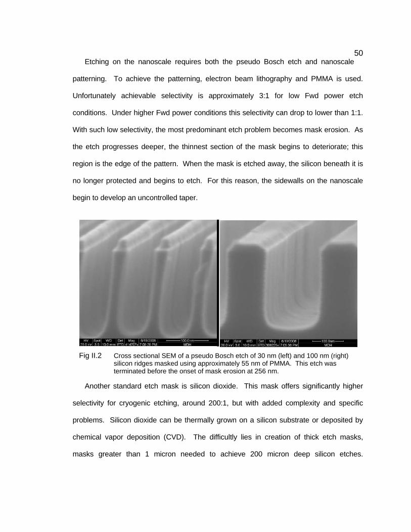
50 Etching on the nanoscale requires both the pseudo Bosch etch and nanoscale
patterning. To achieve the patterning, electron beam lithography and PMMA is used.
Unfortunately achievable selectivity is approximately 3:1 for low Fwd power etch
conditions. Under higher Fwd power conditions this selectivity can drop to lower than 1:1.
With such low selectivity, the most predominant etch problem becomes mask erosion. As
the etch progresses deeper, the thinnest section of the mask begins to deteriorate; this
region is the edge of the pattern. When the mask is etched away, the silicon beneath it is
no longer protected and begins to etch. For this reason, the sidewalls on the nanoscale
begin to develop an uncontrolled taper.
Fig II.2 Cross sectional SEM of a pseudo Bosch etch of 30 nm (left) and 100 nm (right)
silicon ridges masked using approximately 55 nm of PMMA. This etch was terminated before the onset of mask erosion at 256 nm.
Another standard etch mask is silicon dioxide. This mask offers significantly higher
selectivity for cryogenic etching, around 200:1, but with added complexity and specific
problems. Silicon dioxide can be thermally grown on a silicon substrate or deposited by
chemical vapor deposition (CVD). The difficultly lies in creation of thick etch masks,
masks greater than 1 micron needed to achieve 200 micron deep silicon etches.

51 Furthermore, patterning such deep etch masks become difficult. Wet etching of silicon
dioxide using hydrofluoric acid (HF) induces as much lateral undercut as it does vertical
and dry etching requires a second patterning step using chrome etch mask. The
advantage of using silicon dioxide is that removal and wet etching techniques do not
chemically etch the silicon. Although dry etching is preferential to etching silicon dioxide
over that of silicon, it does etch silicon at rates comparable to pseudo Bosch. For this
reason, silicon dioxide etch masks are infrequently used.
Undercutting with Metal Masks
Metal etch masks are used since metals can be very chemically resilient, very hard to
withstand milling, and very easy to pattern since only thin layers are needed. Further,
metal etch masks can be removed using wet chemistry which will not affect the substrate;
achieving the orthogonality requirement. A very good example of a metal used is chrome.
Very thin layers are easily deposited using thermal evaporation or sputtering and can offer
selectivity of 50:1 for silicon dioxide etches. Where metal fails to meet etch requirements
is on the low Fwd power silicon etches. Metal etch masks protect the vertical sidewalls
well but have a severe problem of undercutting. The exact nature of this undercut is
unclear but a very good demonstration is as follows.
Fig II.3 Cross sectional SEM of a cryogenic etch of 10 (left), 20 (middle), and 50 (right)
micron diameter silicon micropillars. The etched height was 30 microns and was

52 masked with chrome. This etch demonstrates a failure of metal etch masks not seen with dielectric etch masks.
A chrome etch mask was thermally evaporated on silicon and patterned using
photoresist and chrome etch. The pattern was the hexagonal pillar pattern, described
earlier. Upon completion of a 30 micron deep cryogenic etch, the chrome mask was
completely undercut. The 10 and 20 micron diameter pillars had their mask completely
undercut and falling off and the 50 micron diameter had an undercut of approximately 15
microns radially. What is most surprising is that the silicon etch was very vertical and
smooth. A second experiment with metal etch masks was performed using thermally
evaporated copper patterned similarly to the chrome mask experiment. The difference
between the two metals is that copper is about 10 times less resistive than that of chrome,
16.78 nano-Ohm-m and 125 nano-Ohm-m respectively. The copper masked silicon was
etched 37 microns deep under similar etching conditions. Although the amount of lateral
undercutting was comparable, the copper masked structure was hollowed out from the
inside and left resembling a chalice as seen from the 20 and 50 micron diameter pillars.
Fig II.4 Cross sectional SEM of a cryogenic etch of 50 (left) and 20 (right) micron diameter
silicon micropillars. The etched height was 37 microns and was masked with

53 copper. This etch demonstrates a failure of metal etch masks not seen with dielectric etch masks.
The fact that dielectric masks such as silicon dioxide and photoresist do not undercut
suggests that this problem could be attributed to electric field perturbation effects. Further,
it is interesting to note that as the conductivity of the metal increases, so does the effect of
the undercut. As previously stated, insertion of a metal plate into a DC and AC electric
field can alter the boundary conditions. What is clear is that a mask undercut will occur
using the cryogenic etch and the pseudo Bosch etch with metal masks, so an alternative is
needed.
Alumina Etch Mask Achieving high aspect ratio silicon nanostructures is rapidly becoming necessary [21].
In order to meet Moore’s Law, fabricating at the nanoscale is critical. Deviations in the
etch much more than a nanometer can result in process failure. It is the author’s vision
that predicts that silicon will be required to be built vertical to maintain the current drive to
higher transistor count per wafer [22]. Bottom-up processing already has the ability to
grow long silicon nanowires with smooth sidewalls. Where this technology is challenged is
that precision placement is difficult. This is not acceptable in current CMOS fabrication
facilities. Top-down processing will need to create silicon structures similar to that
achieved by bottom-up but using tools and material currently integrated in industrial
facilities. It would be interesting to ask a Fab manager if gold could be introduced into a
CMOS Fab line in order to grow silicon nanowires.
Novel nanoscale etching has been very close to achieving the needed nanostructures.
With the invention of passivated silicon etching, such as the cryogenic or pseudo Bosch
etch, smooth vertical sidewalls are achievable [23]. Using extreme UV lithography or

54 electron beam lithography nanoscale patterning is also achievable [24]. What has been
missing is an etch mask which meets all four of the requirements needed: orthogonal
mask etching chemistry from that of the silicon, chemical resilience to fluorinated silicon
etches, milling resilience, and electrically insulating [25].
For these reasons, the aluminum oxide (alumina) etch mask was invented. It was
hypothesized that since alumina is non-conductive, electric field effects would not be
present unlike metal masks. Since alumina is hard, it was expected that it should be
resilient to milling. Further, if fluorine were to bond it would create a nonvolatile AlxFy or
AlFxOy compound which would remain; essentially it would be resilient to fluorine chemical
etch. Finally, since alumina is more glass like than metal, it was predicted that patterning
and liftoff would be easier than with metal. On all these points alumina was successful.
What was unexpected was the alumina mask removal chemistry. After etching alumina
was discovered to be removed using Buffered HF, albeit at a very slow rate. But what was
advantageous was that BHF does not etch silicon [26]. So the idea of orthogonality
between etch chemistry of silicon and alumina was realized with this as an etch mask.
Since the ammonium in BHF was what etched the alumina, it was quickly realized that
ammonium hydroxide and hydrogen peroxide would much more efficiently etch the
alumina. This combination is referred to in industry as RCA 1 clean and is used for
cleaning silicon during wafer fabrication. In one discovery, alumina enabled high aspect
ratio silicon nanostructures to become compatible with mainline semiconductor fabrication
lines.
This section of the chapter will detail fabrication processes of the alumina etch mask
for microscale and nanoscale silicon structures. It will detail the patterning, etching, and

55 removal process and describe the results of using the mask with the cryogenic etch and
the pseudo Bosch silicon etch.
Mask Fabrication Sequence
As stated earlier, both photoresist and cryogenic etching are most suitable for the
microscale. The alumina etch mask integrates well with these two processes. To
demonstrate a possible fabrication sequence, micropillars and micro-holes, identical to the
hexagonal pillar pattern described previously, were fabricated. Using the AZ 5214e resist,
a 1.6 micron thick patterning of holes and circles with diameters 5, 10, 20, and 50 microns
were defined on both P and N type <100> silicon wafers. Patterning using this resist is
detailed in Appendix A. For the nanoscale, it was more appropriate to use PMMA electron
beam resist and pseudo Bosch etching. Nanoscale patterning was performed in 75 nm
thick resist. The patterns consisted of hexagonally packed arrays with pillar separation
double the diameter and square array rows of pillars with decreasing diameters. The
square arrays were marked with 5 to 20 micron diameter pillars at the corners of the
arrays. The patterns were defined using a Leica EBPG with a 100kV electron beam.
Again, both P an N <100> silicon was used.
Alumina was then sputtered on the patterned resist. Sputtering of alumina offers the
advantage of low temperature deposition with the disadvantage that step coverage is very
good. Sputtering was performed using a TES 1800 DC magnetron sputter system, using
a 99.995% aluminum target and a 5:1 mixture of argon to oxygen as the process gas. This
ratio of gases allows for the aluminum to be sputtered without poisoning the target while
still deposits a stoichiometric aluminum oxide. Specifically, the sputtering parameters are
as follows: 100 sccm of Ar, 20 sccm of O2, pressure of 10 to 15 mTorr, and 400 W of DC
power. Lower sputtering power can be used but reduces the sputter rate of approximately

56 10 nm per minute. An aluminum target was used for multiple reasons. Primarily, the
heat generated on the target does not crack an aluminum target like an alumina target;
this is due to the increased thermal conductivity of aluminum over alumina. Secondary is
that aluminum targets are significantly less expensive than alumina targets.
Liftoff is then conducted using Acetone. Placing the sample in a beaker, liftoff is
achieved on timescales of minutes. Adhesion between the silicon and alumina is very
good and permits light scrubbing using Q-tips or cotton swabs. At this point, all that
remains on the silicon substrate is the patterned alumina. If further cleaning is needed, a
low milling oxygen plasma can be implemented to clean the structure. The patterned
sample is now ready for silicon etching.
Fig II.5 SEM of 5 micron diameter alumina etch mask on silicon after liftoff.
Micropillar and Nanopillar Etching Micropillars were etched using a cryogenic etch modified slightly to achieve high
aspect ratio structures. The adjustments are as follows:

57 SF6 70 sccm ICP Power 900 W
O2 7.2 sccm Fwd Power 20 W
Temperature -140 C Pressure 10 mt
Using this chemistry DC bias was 91 V, Eo=0.9843, and b=0.02808 with the two
coefficients calculated with an R-square value of 0.9946. Comparing this set of
parameters with previously stated, it should be noted that Eo decreased as well as b.
Fundamentally, by increasing the oxygen and temperature the passivation increased
which overall slowed the etch rate down 1.14 microns per minute to 0.98 microns per
minute. Interpretation of b as the slowing of the etch rate due to aspect ratio, and
measuring the aspect ratio dependence as a ratio of b to Eo, shows the change of 3.6% to
2.85%. The dependence reduction is attributed to the increased Fwd power.
Fig II.6 Cryogenic etch data for various aspect ratios of silicon micropillars. The data was
width normalized to solve for the E and b coefficients.

58 The alumina etch mask used was 110 nm thick and the highest pillar etch was
143.7 microns tall for a 50 micron diameter pillar. With some resist mask remaining this
yielded a minimum selectivity of 1306:1. The milling rate on the alumina mask was
approximated to less than 0.75 nm per minute given an etch time of 140 minutes.
Measurements were taken in a FEI tools Quanta SEM. Trench aspect ratios of the 5, 10
and 20 micron diameter pillars were 25.3, 12.0, and 7.4 respectively. It should be noted
that the edges of the mask began to fail as evident by the etched marks at the top of the
pillars. The next etch in this sequence for 160 minutes resulted in complete mask erosion.
It should also be noted that very little re-deposition of the alumina mask occurs since very
little black silicon is present.
Fig II.7 Cross sectional SEM of a cryogenic etch of 5 micron diameter silicon micropillars.
The etched height was 83 microns. The alumina mask was approximately 110 nm thick.

59
Fig II.8 Cross sectional SEM of a cryogenic etch of 10 (left) and 20 (right) micron diameter
silicon micropillars. The etched height was 103 and 126 microns respectively. The alumina mask was approximately 110 nm thick.
Fig II.9 Cross sectional SEM of a cryogenic etch of 20 micron diameter silicon micropillars.
The etched height was 30 microns. The alumina mask was approximately 30 nm thick for a selectivity of 1000:1.
By reversal of the same resist from positive to negative, holes in an identical pattern
as that of the pillars was also etched. Etch conditions were again slightly altered with a

60 decrease in Fwd power to 10 W and etched for 1 hour. The alumina etch mask was
deposited for 2 minutes for an approximately 20 nm thick mask. The 5 micron diameter
holes were etched 41 microns deep and the 20 nm holes were etched 64 nm deep. This
yields a selectivity of approximately 3200:1. The hourglass like shape at the top of the 5
micron holes is attributed to cleaving the holes off center.
Fig II.10 Cross sectional SEM of a cryogenic etch of 5 (left) and 20 (right) micron diameter
silicon holes. The etched height was 41and 64 microns respectively. The alumina mask was approximately 20 nm thick.
To create the silicon nanopillars, the pseudo Bosch etch was employed since the etch
rate was significantly slower and more controlled. The etch used is as follows:
SF6 33 sccm ICP Power 1200 W
C4 F8 57 sccm Fwd Power 20 W
Temperature 15 C Pressure 10 mt
Using this etch, silicon nanopillars and nanowires were fabricated down to 20 nm
diameters and pillar aspect ratios over 60:1. The etch rate for these etch conditions

61 yielded an etch rate of approximately 300 nm per minute. Error bars indicate the range
of etch heights over all the trench aspect ratios over the etch. Changes in the fwd power
do have dramatic changes in the etch rate, however, so caution should be taken when
varying conditions.
Fig II.11 Pseudo Bosch etch data averaged over all the aspect ratios of silicon nanopillars.
As a first example of the quality achievable with the mask, rows of 40 and 65 nm pillars
were etched 3 minutes to 780 nm heights. The pillars were hexagonally packed and
spaced at twice the diameter. As a second example to demonstrate the improvement of
alumina etch masks over masks such as nickel, an experiment was performed using both
etch masks under identical etch conditions described above. Approximately 80 nm
diameter pillars arranged in a hexagonal packed array were etched to similar heights.
What should be noticed is that the tops of the pillars are dramatically different. The nickel
etch masked pillars have sharp point and severe undercutting where as the alumina etch
masked pillars have flat smooth tops with little to no undercutting.

62
Fig II.12 Cross sectional SEM of a pseudo Bosch etch of silicon nanopillars. The pillar
diameters alternated between 40 and 65 nm and were etched 780 nm tall. The alumina etch mask used was 30 nanometers thick.
Fig II.13 Demonstration of the difference between a nickel etch mask (left) and alumina etch
mask (right). Cross sectional image of approximately 80 nm diameter pillars etched to 970 nm (left) and 780 nm (right). The etch conditions were identical. Note the mask undercut problems of the nickel mask are not present on the alumina etch mask.
To measure the surface roughness of the etched sidewalls, bright field reflection
electron microscopy was performed on the nanopillars. By mounting the silicon
nanopillars sideways in a FEI TEM, the sample could be imaged without removing it from

63 the substrate. The images taken display notching of less than 5 nm and with the peak
surface roughness approximately a few nanometers.
Fig II.14 Bright field reflection microscopy of a 100 nm diameter pillar taken in a FEI
transmission electron microscope. The pillar was etched using the pseudo Bosch silicon etch and masked using alumina. Not the image is rotated approximately 60 degrees.
Although the previous pillar pattern was useful in characterizing the etch mask and
etch, separation of the pillars was desired for mechanical and electrical characterization.
For characterization, the pillars were separated by 5 micron with rows which descended in
sizes from approximately 420 nm diameters down to 20 nm in diameter in 40 nm
increments and back up to 180 nm diameters in 20 nm increments with 14 pillars in each
row. The arrays had 20 micron diameter pillars located on the edges of the array to serve
as markers. Using this array, silicon nanowires with aspect ratios greater than 60:1 and
with diameters down to 20 nm were fabricated using this top-down method. As an
example, a 57 nm nanowire was etched 2.54 microns high with a positive taper of 90.6
degrees and an aspect ratio of 45:1. This patterning permitted testing of pillars with
identical heights but varying diameters; for example a sample with 52 nm, 114 nm, 152
nm, and 206 nm diameter pillars etched 2.1 microns in length.
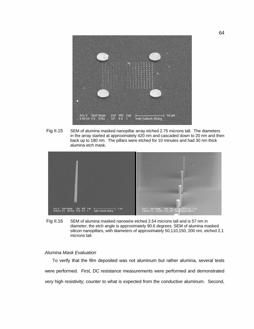
64
Fig II.15 SEM of alumina masked nanopillar array etched 2.75 microns tall. The diameters
in the array started at approximately 420 nm and cascaded down to 20 nm and then back up to 180 nm. The pillars were etched for 10 minutes and had 30 nm thick alumina etch mask.
Fig II.16 SEM of alumina masked nanowire etched 2.54 microns tall and is 57 nm in
diameter; the etch angle is approximately 90.6 degrees. SEM of alumina masked silicon nanopillars, with diameters of approximately 50,110,150, 200 nm, etched 2.1 microns tall.
Alumina Mask Evaluation
To verify that the film deposited was not aluminum but rather alumina, several tests
were performed. First, DC resistance measurements were performed and demonstrated
very high resistivity; counter to what is expected from the conductive aluminum. Second,

65 stoichiometry of the sputtered alumina was determined using energy dispersive X-ray
spectroscopy (EDX). Analysis of the spectrum indicates that the etch mask is within 0.6%
of stoichiometric alumina with a ratio of oxygen to aluminum very nearly 3:2. Although it is
not a qualitative test, comparison between the nickel and alumina etch mask
demonstrated that the alumina mask does not seem to be as conductive as the nickel.
Fig II.17 EDAX measurement of the sputtered alumina film. The peaks are centered around Oxygen, Aluminum, and Silicon with a ratio of nearly 3:2 of Oxygen to Aluminum; the same as stoichiometric alumina.
The most significant advantage of using this mask for fluorinated silicon etch
chemistries is the achievable selectivity. For the cryogenic etch a 20 nm thick alumina
mask is used to etch more than 64 microns into the silicon wafer before mask erosion
begins. From this etch a lower bound on the alumina to silicon selectivity of over 3200:1.
As a further demonstration of the resiliency of the etch mask, 300 nm of alumina is used to
etch 50 micron diameter holes through a 350 micron wafer. A 110 nm thick alumina mask

66 began to erode after 160 minutes of cryogenic etching using 20 Watts of Fwd power;
the 50 micron diameter pillar final etch height was 126 microns. This selectivity is a
significant improvement over photo resist’s selectivity of approximately 100:1; a factor of
32 improvement.
For the Pseudo Bosch etch chemistry, typical values of selectivity for PMMA are 5:1.
Using an alumina etch mask of 30 nm, nanoscale pillars were etched to heights of 2.75
microns yielding a selectivity of better than 91:1. This is a factor of 18 in improvement.
Focused Ion Beam Implanted Gallium Etch Masks Creating top-down fabricated nanoscale structures has predominantly required
electron beam lithography patterning of resist to define the structure. This method
requires a planar surface so that the resist may be planarized by spinning. Once the
pattern is spun it is patterned using an electron beam, either from a modified SEM or an
EBPG. After writing, the resist is chemically developed in a solution that removes the
cross linked resist leaving a patterned substrate. Upon completion of the fabrication
sequence, such as ICP etching, the etch mask needs to be removed by either oxygen
plasma or wet chemistry. This fabrication sequence is troublesome for multiple reasons.
First the requirement of a planar surface severely restricts when this step may occur. For
example, re-patterning of etched silicon is extremely difficult and time consuming.
Second, this patterning technique requires the use of wet chemistry which always leaves a
chemical residue and can limit the structures achievable. As an example of this, wet
chemistry involving nanowires typically leaves the wires sticking together due to surface
forces. Furthermore, wet chemistry inevitably requires more chemical waste; a current
ecological problem.

67 When fluorine or oxygen chemically bonds to gallium, it forms a nonvolatile GaFx or
GaOx respectively. This property enables the Ga implantation to act as a fluorine or
oxygen etch mask. This aspect has been explored for wet etching of silicon using
potassium hydroxide (KOH) and HF; the mask demonstrated chemical etch resistance.
This etch resistance was explored for use as an ICP etch mask. To pattern the Ga mask,
a Focused Ion Beam was used to implant the Ga with resolution to better than 30 nm.
This chapter describes the implantation and etches viable using this concept enabling a
dry lithography.
Admittedly, this technique produces extreme damage to silicon. However a significant
amount of work and time has been spent understanding the damage and methods to
repair. Although this work is outside of the scope of this thesis, a very good list of
references can be found from the SRIM and TRIM website. Finally, it should be
emphasized that the technique of implanting ions as an etch mask is not limited to Ga and
Si. This method can be extended to SiO2, diamond, graphite, carbon nanotube, etc. The
critical idea is that the implanted ion and the etching ions need to form a nonvolatile
compound under ICP etch conditions which favor chemical etching over milling.
Ga Implantation using a FIB
One alternative has been a combination of patterning and etching using a Focused Ion
Beam, FIB. A FIB draws atoms from either a precursor gas or liquid, ionized the gas,
accelerates the ion using a voltage potential, and then collimates the beam of ions.
Deflection of the beam using either magnetic or electrostatic lenses permits precision
control over beams. The achievable beam waists and control over the beams trajectory
have been reduced down to a few nanometers. The method of accelerating and control of
these ion beams is akin to electron beam control used in SEMs or EBPGs. By changing

68 the dwell time or the beam current the amount of ions driven to a sample can be
modified. Many FIB’s utilize an ion beam of Gallium, Ga, electrostatically pulled from a
liquid metal source. When this beam is applied to substrates such as silicon, silicon
dioxide, silicon dioxide or metal, the impact of the Ga ion can remove substrate atoms.
This is referred to as milling. If the energy of the impact, or number or impacts, is not
enough to remove the substrate the ion is said to have been implanted in the substrate.
Implantation is similar to a meteor crashing into earth, if the size and velocity of the meteor
is small enough, the meteor will continue to bury itself in the earth until it comes to a stop.
The trajectory path is filled with damaged and disarray. This is analogous to what occurs
with silicon. The Ga atom can travel into the silicon substrate, leaving amorphous silicon
in its wake, and come to rest at a given location in the silicon. By controlling where these
impacts occur, the energy of the impacts, and the number of impacts occurring, a Ga layer
in the silicon can be defined. This patterned Ga layer can then be used to protect the
silicon below it from other impacting ions of lesser energy and from chemical reactions.
This is the basis of the implanted Ga etch mask.
Patterning of the Ga etch mask was accomplished using the dual beam Nova
FIB/SEM by FEI. A cleaned silicon sample is placed at the eucentric height and rotated
such that the ion beam strikes perpendicular to the substrate surface. For a selected beam
current, the Ga+ beam is focused at the edge of the substrate. Automated write programs
specifying the pattern and dwell times are then executed to raster the ion beam. In a
manner analogous to a scanning electron microscope, the FIB accelerates the Ga+ ions to
the surface of the silicon substrate using various accelerating beam voltages. The
magnitude of the beam voltage controls both the implantation depth and the thickness of
the Ga layer.
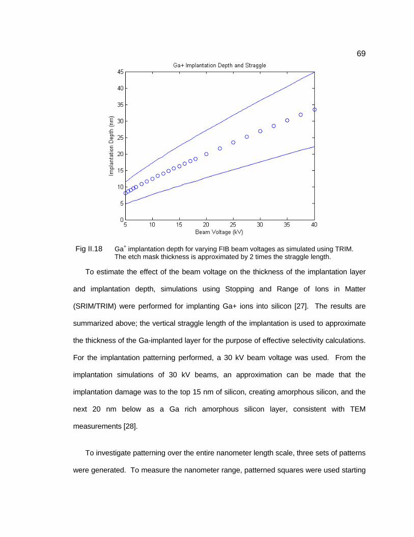
69
Fig II.18 Ga+ implantation depth for varying FIB beam voltages as simulated using TRIM.
The etch mask thickness is approximated by 2 times the straggle length.
To estimate the effect of the beam voltage on the thickness of the implantation layer
and implantation depth, simulations using Stopping and Range of Ions in Matter
(SRIM/TRIM) were performed for implanting Ga+ ions into silicon [27]. The results are
summarized above; the vertical straggle length of the implantation is used to approximate
the thickness of the Ga-implanted layer for the purpose of effective selectivity calculations.
For the implantation patterning performed, a 30 kV beam voltage was used. From the
implantation simulations of 30 kV beams, an approximation can be made that the
implantation damage was to the top 15 nm of silicon, creating amorphous silicon, and the
next 20 nm below as a Ga rich amorphous silicon layer, consistent with TEM
measurements [28].
To investigate patterning over the entire nanometer length scale, three sets of patterns
were generated. To measure the nanometer range, patterned squares were used starting

70 at 500 nm and ending at 50 nm stepped in 50 nm increments. The dose columns
began at 5.3*1015 cm-2 and ended in 1.96*1017 cm-2 with the dose stepped in
approximately 1*1016 cm-2 increments. To determine sub 200 nm resolution, patterned
squares were again used starting at 200 nm and ending at 20 nm stepped in 20 nm
increments. The third pattern arrays were circles starting at 100 nm in diameter and
ending at 10 nm in diameter stepped in 10 nm increments. Both the second and third
pattern arrays, the dose column began with 1.25*1016 cm-2 and ended in 1.25*1017 cm-2
with the dose stepped in approximately 1.25*1016 cm-2 increments using a measured 6.87
pA beam.
For the micron scaled structures we created dose arrays of 5 micron by 5 micron
squares separated by approximately 10 microns. Each square dose was varied by
incrementing the write time 2 second. With the beam current at 100 pA, this provided a
dose step of 5*1016 cm-2. The dose array began at 1*1016 cm-2 and stopped at 5*1016 cm-2.
After implantation, verification of the patterning can be seen using a scanning electron
microscope (SEM).
Silicon Etching
Pseudo Bosch Silicon Etching Investigation into the potential for nanoscale patterning utilized the pseudo Bosch etch
for reasons mentioned earlier. As a verification that the type and amount of doping in
silicon wafers was unimportant, several different Si samples were used, N-doped <100>
rho=1-10 Ohm-cm and P-doped <100> rho=0.005 Ohm-cm. Patterned samples were
placed on a 6 inch silicon carrier wafer using Fomblin oil as an adhesive and thermal
conductor. The first dose array was etched under the following conditions:

71 SF6 33 sccm ICP Power 1200 W
C4 F8 50 sccm Fwd Power 10 W
Temperature 15 C Pressure 10 mt
This etch chemistry had a measured forward bias of 54 volts. The second and third
dose arrays were etched under identical etching conditions as before, except Fwd power
was increased to 15 W and the C4F8 gas was increased to 68 sccm; this modification
improved pattern fidelity for sub 100 nm structures. Upon completion of etching, the
Fomblin was removed using IPA and the sample imaged using either the FEI Nova 600 or
a FEI Sirion SEM.
Fig II.19 Scanning electron micrograph of a dose array for nanoscale SF6/C4F8 etch. Etch
depth was 460 nm with the squares ranging from 500 nm down to 50 nm in 50 nm increments. Inset is a scanning electron micrograph of Ga implanted nanoscale dose array in silicon. The large square was where the ion beam was focused and used as a visual marker.
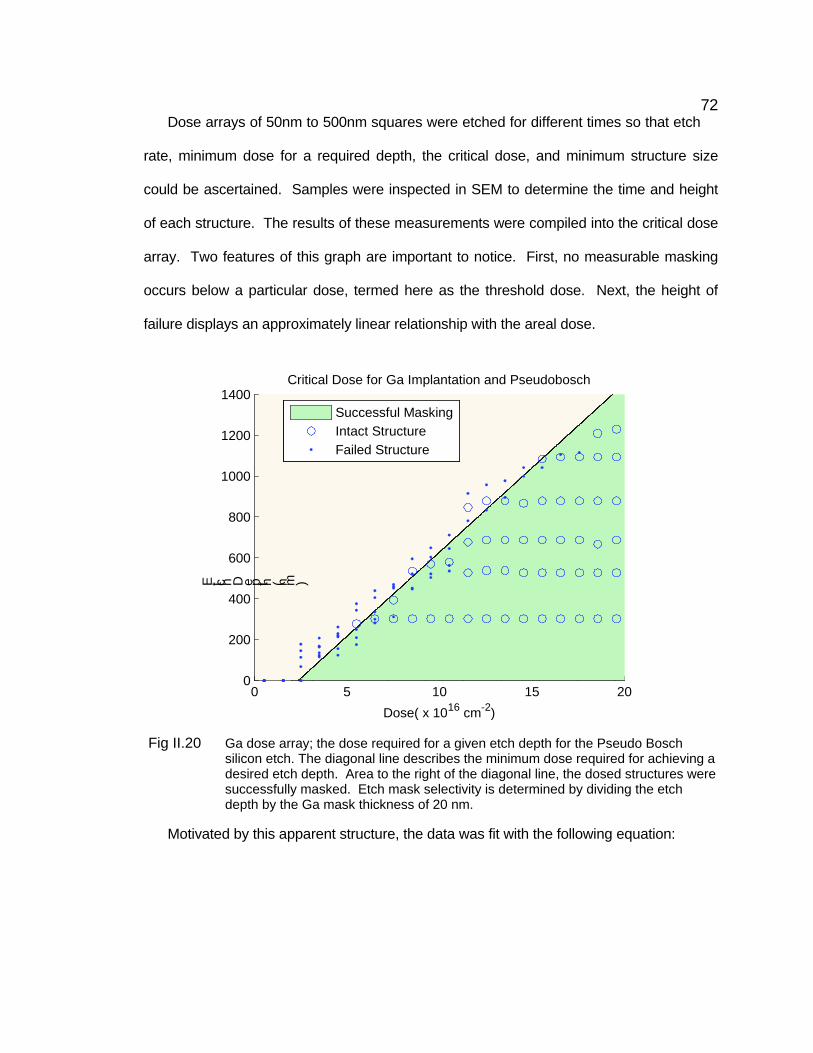
72 Dose arrays of 50nm to 500nm squares were etched for different times so that etch
rate, minimum dose for a required depth, the critical dose, and minimum structure size
could be ascertained. Samples were inspected in SEM to determine the time and height
of each structure. The results of these measurements were compiled into the critical dose
array. Two features of this graph are important to notice. First, no measurable masking
occurs below a particular dose, termed here as the threshold dose. Next, the height of
failure displays an approximately linear relationship with the areal dose.
Fig II.20 Ga dose array; the dose required for a given etch depth for the Pseudo Bosch
silicon etch. The diagonal line describes the minimum dose required for achieving a desired etch depth. Area to the right of the diagonal line, the dosed structures were successfully masked. Etch mask selectivity is determined by dividing the etch depth by the Ga mask thickness of 20 nm.
Motivated by this apparent structure, the data was fit with the following equation:
0 5 10 15 200
200
400
600
800
1000
1200
1400
Dose( x 1016 cm-2)
E t c h D e p t h ( n m )
Critical Dose for Ga Implantation and Pseudobosch
Successful MaskingIntact StructureFailed Structure
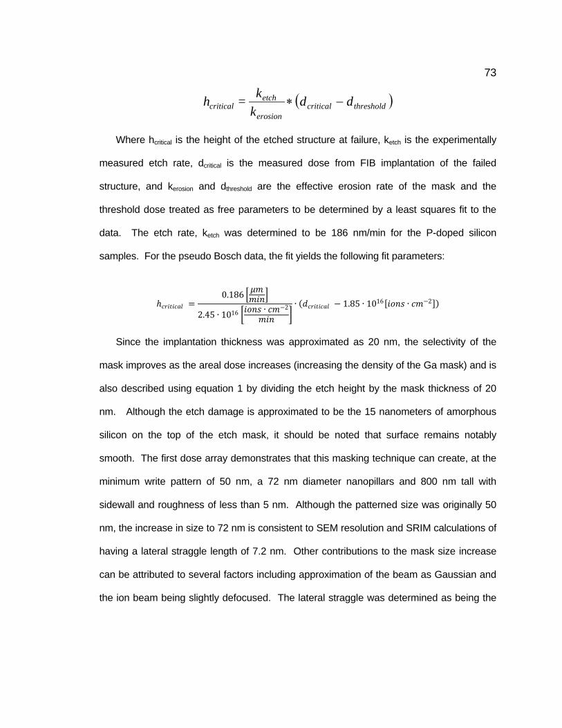
73
( )thresholdcriticalerosion
etchcritical dd
kk=h −∗
Where hcritical is the height of the etched structure at failure, ketch is the experimentally
measured etch rate, dcritical is the measured dose from FIB implantation of the failed
structure, and kerosion and dthreshold are the effective erosion rate of the mask and the
threshold dose treated as free parameters to be determined by a least squares fit to the
data. The etch rate, ketch was determined to be 186 nm/min for the P-doped silicon
samples. For the pseudo Bosch data, the fit yields the following fit parameters:
ℎ𝑐𝑐𝑐𝑐𝑐𝑐𝑑𝑑𝑐𝑐𝑐𝑐𝑎𝑎𝑠𝑠 =0.186 𝜇𝜇𝜇𝜇𝜇𝜇𝑐𝑐𝐿𝐿
2.45 ∙ 1016 𝑐𝑐𝑐𝑐𝐿𝐿𝑠𝑠 ∙ 𝑐𝑐𝜇𝜇−2
𝜇𝜇𝑐𝑐𝐿𝐿 ∙ (𝑃𝑃𝑐𝑐𝑐𝑐𝑐𝑐𝑑𝑑𝑐𝑐𝑐𝑐𝑎𝑎𝑠𝑠 − 1.85 ∙ 1016[𝑐𝑐𝑐𝑐𝐿𝐿𝑠𝑠 ∙ 𝑐𝑐𝜇𝜇−2])
Since the implantation thickness was approximated as 20 nm, the selectivity of the
mask improves as the areal dose increases (increasing the density of the Ga mask) and is
also described using equation 1 by dividing the etch height by the mask thickness of 20
nm. Although the etch damage is approximated to be the 15 nanometers of amorphous
silicon on the top of the etch mask, it should be noted that surface remains notably
smooth. The first dose array demonstrates that this masking technique can create, at the
minimum write pattern of 50 nm, a 72 nm diameter nanopillars and 800 nm tall with
sidewall and roughness of less than 5 nm. Although the patterned size was originally 50
nm, the increase in size to 72 nm is consistent to SEM resolution and SRIM calculations of
having a lateral straggle length of 7.2 nm. Other contributions to the mask size increase
can be attributed to several factors including approximation of the beam as Gaussian and
the ion beam being slightly defocused. The lateral straggle was determined as being the
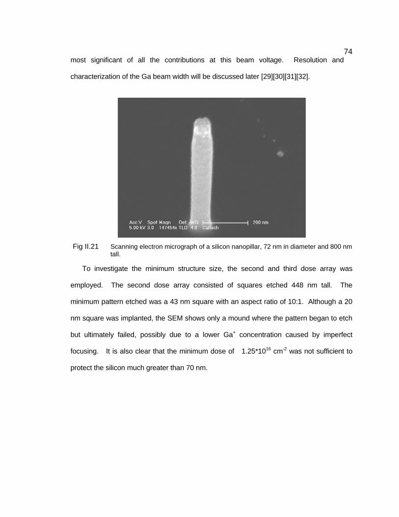
74 most significant of all the contributions at this beam voltage. Resolution and
characterization of the Ga beam width will be discussed later [29][30][31][32].
Fig II.21 Scanning electron micrograph of a silicon nanopillar, 72 nm in diameter and 800 nm
tall.
To investigate the minimum structure size, the second and third dose array was
employed. The second dose array consisted of squares etched 448 nm tall. The
minimum pattern etched was a 43 nm square with an aspect ratio of 10:1. Although a 20
nm square was implanted, the SEM shows only a mound where the pattern began to etch
but ultimately failed, possibly due to a lower Ga+ concentration caused by imperfect
focusing. It is also clear that the minimum dose of 1.25*1016 cm-2 was not sufficient to
protect the silicon much greater than 70 nm.

75
Fig II.22 Scanning electron micrograph of second dose array for nanoscale SF6/C4F8 etch.
Etch depth was 448 nm with the squares ranging from 200 nm down to 20 nm in 20 nm increments.
The third dose array patterns were circles for vertical silicon nanowire fabrication and
were etched simultaneously with the second dose array pattern. The minimum pattern
etched was the 31 nm diameter pillar. The etch was reentrant at 89.15 degrees causing
the base of the pillar to be at an 18 nm diameter. Although it is clear that significant
masking occurred for the 20 nm pattern, the reentrant angle did not permit the structure to
withstand the etch. Important to note is the higher fidelity of this patterning as compared to
previous demonstrations.

76
Fig II.23 Scanning electron micrograph of third dose array for nanoscale SF6/C4F8 etch.
Etch depth was 448 nm with the pillars ranging from 100 nm down to 10 nm diameters in 10 nm increments.
This etch attained a very high selectivity with no oxygen in the etch chemistry. This is
contrary to the masking mechanism of GaOx forming at the surface proposed elsewhere
[33]. Formation of a GaOx layer during sample exposure to ambient is also excluded due
to the 28nm implantation depth. This leads us to hypothesize another masking
mechanism. Fluorine can bond with the Ga to create an involatile GaFx mask, which may
also contribute to further physical sputtering resistance. This is consistent with previous
results using reactive ion etching with SF6 which relies on F+ ions for etching [33,34,35].
Cryogenic Silicon Etching Using the same etching system and mounting techniques as the nanoscale etch,
micron sized features were also etched to determine the etch rate and threshold dose for a
required depth. The cryogenic etch was employed for this scale. The etch conditions
used are as follows:
SF6 70 sccm ICP Power 900 W

77 O2 6.5 sccm Fwd Power 10 W
Temperature -130 C Pressure 10 mt
This etch chemistry had a measured DC bias of 54 volts. The cryogenic dose array,
described earlier, was etched for etch times of 1, 3, 10, 20 and 40 minutes with a
measured etch rate, ketch, of 1.03 microns per minute; the results compiled in the cryogenic
critical dose array.
Fig II.24 Ga dose array; the dose required for a given etch depth for the Cryogenic silicon
etch. The diagonal line describes the minimum dose required for achieving a desired etch depth. Area to the right of the diagonal line, the dosed structures were successfully masked. Etch mask selectivity is determined by dividing the etch depth by the Ga mask thickness of 20 nm.
The Fwd power, and subsequently the bias voltage, was intentionally set to match that
of the pseudo Bosch etch with the other etching parameters set to optimize the etch.
Although the ICP and gas chemistry changes the plasma density, matching the bias
1 1.5 2 2.5 3 3.5 4 4.5 50
5
10
15
20
25
30
35
40
45
Dose( x 1016 cm-2)
E t c h D e p t h ( u m )
Critical Dose for Ga Implantation and Cryogenic Etch
Successful MaskingIntact StructureFailed Structure

78 voltages allows for the milling aspect of the two etch chemistries to be more closely
compared.
ℎ𝑐𝑐𝑐𝑐𝑐𝑐𝑑𝑑𝑐𝑐𝑐𝑐𝑎𝑎𝑠𝑠 =1.03 𝜇𝜇𝜇𝜇𝜇𝜇𝑐𝑐𝐿𝐿
0.06736 ∙ 1016 𝑐𝑐𝑐𝑐𝐿𝐿𝑠𝑠 ∙ 𝑐𝑐𝜇𝜇−2
𝜇𝜇𝑐𝑐𝐿𝐿 ∙ (𝑃𝑃𝑐𝑐𝑐𝑐𝑐𝑐𝑑𝑑𝑐𝑐𝑐𝑐𝑎𝑎𝑠𝑠 − 2.2 ∙ 1016[𝑐𝑐𝑐𝑐𝐿𝐿𝑠𝑠 ∙ 𝑐𝑐𝜇𝜇−2])
Interestingly, dthresold is nearly the same for both etch chemistries (2.2*1016 ions*cm-2 as
compared to 1.85*1016 ions*cm-2), while kerosion for the cryogenic etch is nearly two orders
of magnitude lower than for pseudo Bosch. This threshold dose, etched with 10 W of
Fwd power, is consistent to that reported by Chekurov et al. [34] whom etched with 2-3 W
of Fwd power and with an etch rate approximately double of that reported here.
Fig II.25 Scanning electron micrograph of a dose array the cryogenic etch. Etch depth was
10.1 μm with 5 μm squares. The dose was varied in this array from 1x1016 cm-2 to 5x1016 cm-2 in 0.5x1016 cm-2 increments.
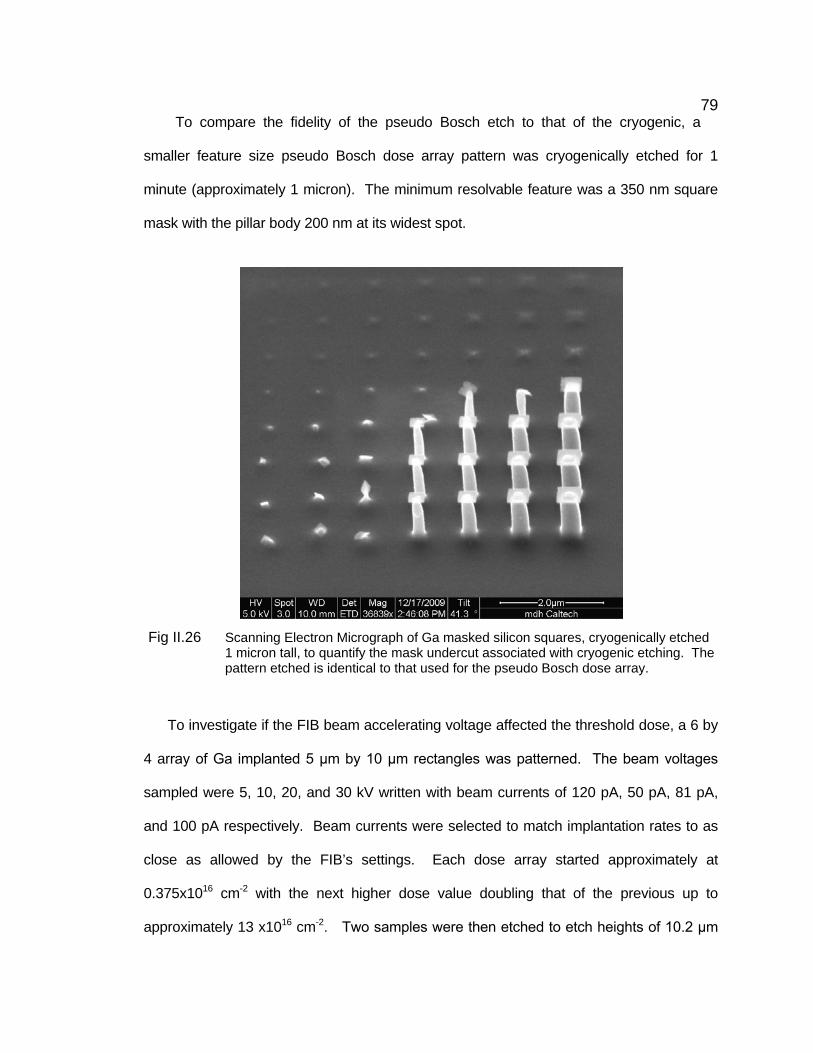
79 To compare the fidelity of the pseudo Bosch etch to that of the cryogenic, a
smaller feature size pseudo Bosch dose array pattern was cryogenically etched for 1
minute (approximately 1 micron). The minimum resolvable feature was a 350 nm square
mask with the pillar body 200 nm at its widest spot.
Fig II.26 Scanning Electron Micrograph of Ga masked silicon squares, cryogenically etched
1 micron tall, to quantify the mask undercut associated with cryogenic etching. The pattern etched is identical to that used for the pseudo Bosch dose array.
To investigate if the FIB beam accelerating voltage affected the threshold dose, a 6 by
4 array of Ga implanted 5 μm by 10 μm rectangles was patterned. The beam voltages
sampled were 5, 10, 20, and 30 kV written with beam currents of 120 pA, 50 pA, 81 pA,
and 100 pA respectively. Beam currents were selected to match implantation rates to as
close as allowed by the FIB’s settings. Each dose array started approximately at
0.375x1016 cm-2 with the next higher dose value doubling that of the previous up to
approximately 13 x1016 cm-2. Two samples were then etched to etch heights of 10.2 μm

80 and 20.1 μm under the same conditions as before but with a reduced Fwd power of 3
W. Reduction of the Fwd power increased the slope of the dose array, maximizing etch
mask selectivity, to amplify any etch height changes due to beam voltage. A failure of the
etch mask during cryogenic etching rapidly destroys the structure, so for this experiment a
loss of etch mask denoted a failure. For the 10.2 μm etch, the 5, 10, 20 and 30 kV
structures required a minimum dose of 2.1x1016 cm-2 , 1.6x1016 cm-2 , 1.6x1016 cm-2 and
0.75x1016 cm-2 respectively. For the 20.1 μm etch, the 5, 10, 20 and 30 kV structures
required a minimum dose of 2.1x1016 cm-2,1.6 x1016 cm-2 , 0.8x1016 cm-2 and 1.6x1016 cm-2
respectively. There is a possible trend of slightly improved masking ability for higher beam
voltages. Different accelerating voltages do result in different ion straggles and thus
different effective Ga layer thicknesses, an etch mask thickness increase due to beam
voltage increase. Although this experiment requires more data for clarification of how the
masking mechanism depends on the implantation voltage, from this we concluded that if
beam voltage did affect the critical dose, it would be by an acceptable value of less than
1.35x1016 cm-2 for a 5 to 30 kV beam voltage shift with a previously determined threshold
dose of 2.2x1016 cm-2.
Multilevel and Grayscale Lithography One of the most significant advantages of using Ga implanted etch masks is that
unlike photolithography, which requires a planar surface for effective spin coating and
exposure, the FIB can pattern non-planar structures. A second advantage of Ga masking
is the linear relationship of etch depth to dose beyond the threshold dose. Utilizing these
two advantages, we demonstrate the feasibility of three dimensional structures in silicon
using multiexposure and grayscale etch masking.

81 Since the Ga beam does not require a polymer resist in which to define a pattern,
one may perform multiple implantations for etch masking regardless of sample surface
topography. Experimentally, this fabrication procedure proceeds as follows: implant initial
mask, etch the silicon, implant second pattern, and etch the silicon. This repeating
sequence can continue for as long at the Ga etch mask remains. Re-implantation of
previous structures can also extend the critical height for these structures.
This technique was demonstrated using a mixture of both the pseudo Bosch and the
cryogenic etch to create a suspended silicon nanowire connected to two pads. First, two
10 micron diameter circles separated by 10 microns were Ga implanted at a dose of
2*1017 cm-2. The structure was then etched to a height of 0.5 microns using the pseudo
Bosch etch. A Ga mask was then implanted in the shape of a rectangle connecting the
two pillars with the same dose as the circles. A mask undercutting cryogenic etch was
then performed for an etch height of 5 microns; this step utilized the undercut to remove all
unmasked silicon below the rectangle. The resulting structure was an 80 nm by 20 nm
silicon nanowire suspended between two 10 μm diameter pillars etched 5 μm tall with the
nanowire connected half a micron below the pillar tops. This technique utilized the
advantages of each etch, the high pattern fidelity of the pseudo Bosch etch and the
inherent undercutting and high selectivity of the cryogenic etch.

82
Fig II.27 Scanning electron micrograph 10 micron diameter silicon pillars, etched 5 microns
tall, with an 80 by 20 nm silicon nanowire suspended in between. The wire is connected 500 nm below the tops of the pillars.
A second applicable technique is the creation of graded structures which utilizes the
observation of the etch depth’s linear dependence on the critical dose. Here, the
structures are dosed to different critical doses and etched to the desired height. At the
heights corresponding to their critical dose the structures will then start to etch at the same
rate as the substrate, in a manner similar in principle to grayscale lithography [32,36].
These implanted structures can then be etched to create sloped features such as blazed
gratings and optical lenses. This idea was demonstrated using nine 5 micron squares
arranged in a row. Each square’s dose was increased approximately 2.5*1016 cm-2 more
than it neighbor square for a dose ranging from 2.5 - 22.5 *1016 cm-2 and etched using the
pseudo Bosch etch. This created a stair step set of platforms.

83
Fig II.28 Scanning electron micrograph 5 μm squares with varied doses. When the etch
depth increases over the critical dose depth, the structure begins to etch but maintains its relative height to its neighbor.
Resolution limitations and masking mechanism The theoretical limit to the highest resolution structures is highly dependent on the
beam spot size and the accelerating beam voltage. These two parameters define the
effective implantation masking area, as the spot size establishes the kernel to be
convolved with the desired dose profile and the accelerating voltage determines the further
spread of ions after interacting with the silicon. For the FIBs at Caltech, a theoretical
resolution limit can be estimated by summing these dimensions in quadrature [30]:
dsystem2 = dspot
2 + dion2
For the minimum spot size dspot=5nm and lateral ion spread at 5kV dion=3.2nm+1.8nm
(1sigma straggle), resulting is dsystem = 7.07nm. For these experiments at 30kV,
dion=9.9+5.6nm, resulting in dsystem = 16.2 nm, as compared to the minimum realized

84 structure of 43 nm. This analysis does not take into account any excess resolution loss
from deflection error, exposure scheme (amount of overlap between shots was 50%),
defocus, or other experimental parameters which may account for the measured minimum
[29,37].
To achieve the greatest etch depths, and hence highest selectivity, the amount of Ga
present in the top layer should be maximized. However, further exposure of the beam
past a certain dwell time leads to a steady state where the influx of Ga+ is balanced by the
sputtered Ga. The amount of Ga present in the silicon sample, areal dose, as a function
of total ion flux for a 30kV beam is seen below. This is approximated from the total flux of
Ga atoms minus the sputtered Ga atoms, using the composition-dependent sputter yield
computed by Monte Carlo simulation [38].
Fig II.29 Plot of implanted dose as a function of incident dose, with limiting value is 3*1017
Ga atoms-cm-2.
As expected, for low doses the areal dose implanted is linear with total flux, as the
sputtered material has a relatively low concentration of Ga relative to the amount

85 implanted. However, as the sputtered depth approaches the mean implantation depth
of 27 nm, the total concentration of Ga in the sputtered material increases. By 28.4 nm,
the areal concentration is 1017 Ga atoms-cm-2, which is lower than total incident flux by
16%. The Ga sputter yield rapidly increases from this point, requiring an enormous
amount of incident flux to increase the implanted concentration. As an example, doubling
the concentration from 1017 to 2*1017 Ga atoms-cm-2 requires more than five times the
incident flux leading to a mask 144 nm below the surrounding substrate. The maximum
implanted value at steady state, calculated to be 3*1017 Ga atoms-cm-2, is dependent on
the ratio of the mean implantation depth and the sputter yield. For the two silicon etch
chemistries described, this leads to a theoretical maximum etch depth of 3406 nm for the
pseudo Bosch chemistry and 425 μm for the cryogenic etch chemistry and a maximum
effective selectivity of 85 and 10625 respectively assuming a 40 nm mask layer. However,
practically achievable figures will be lower, as determined by fidelity requirement and the
point of diminishing returns in implantation, where the selectivity increase is less than the
amount milled by the Ga beam.
Based on SRIM simulations, the 1-sigma average density of Ga assuming no phase
segregation or preferential removal of silicon is approximately 14% of the density of a pure
Ga layer. However, silicon’s low solubility in Ga is well known [39], so the assumption of
complete segregation of the implanted Ga combined with measured Ga lattice constants
leads to a figure of 5.11 - 8.66 equivalent monolayers of Ga present at the threshold dose.
This leads the authors to speculate that the etch masking mechanism is the formation of a
contiguous Ga layer that forms involatile compounds in fluorine-based chemistries and
fails once the layer is breached via physical sputtering of the mask.

86 C h a p t e r I I I
Nanometer Scaled Devices Etching silicon nanostructures using top-down fabrication techniques enabled creating
precisely patterned arrays for investigation of nanoscale properties. Moreover, control
over nanowire lengths for nanowire diameters down to 20 nm is significantly more
repeatable compared to bottom-up growth. On the same sample it is possible to prepare
identical or different diameter nanowires of precisely the same length in any given pattern.
Given this advantage, nanowire arrays for electrical probing of individual pillars became
possible using a probe station mounted in a Quanta SEM.
Although precision in situ electrical measurements of the vertical nanowires have proven
difficult, observations made during probing has spun off many interesting avenues. This
chapter will detail characterization of electrical probing of the silicon nanowires using this
new method and its advantages for vertical devices. Rapid fabrication of lateral silicon
beams using the Ga implantation will also be discussed along with some measurements to
describe their properties.
Vertical Silicon Nanowires Alumina Etch Masked Nanowires
Establishing etch control for the silicon nanowires was interesting, but as soon as they
were fabricated it was pondered if they could be used for devices such as vertical silicon
transistors. Before the transistors could be designed however, an understanding of the
conduction and contact properties was needed. Nanoscale conduction is not the same as
it is on the micron scale. It has been observed for lateral devices that as the surface to
volume ratio decreases, surface states become more significant. As the nanoscale

87 regime is reached, the unpassivated surface states have the theoretical potential to
completely stop conduction. This section will describe how the nanowires fabricated using
the alumina etch mask were measured, some of the surprising results observed, and
possible routes forward for improving the silicon nanowires.
Fabrication of the silicon nanowires follows that described in the alumina etch mask
section. All of the vertical nanowires and nanopillars described in this section utilized P+
silicon with resistivities of 5 to 20 mΩ-cm. Upon completion of etching, the alumina etch
mask was removed using a RCA-1 and BHF clean cycle, detailed in Appendix A [40].
Upon completion of the clean, gold was thermally evaporated on the backside of the
silicon at a rate of 5 Angstroms per second. The thickness of the metal was until a glass
cover slide was no longer optically transparent, approximately 50-100 nm. Layout of the
pillars was arranged such that each pillar diameter would be repeated 8-10 times in the ‘x’
direction. The pillars were also arranged in ‘y’ to start at a 400 nm diameter and decrease
in approximately 40 nm steps down to 20 nm diameter. The samples then increased in 20
nm increments up to 200 nm. Since each pillar was etched simultaneously, the array
provided a range of pillar diameters with identical lengths. Spacing between rows of pillars
was set to 5 microns and spacing of pillars in the row was set to 2 microns.

88
Fig III.1 Scanning electron micrograph of a silicon nanowire array, etched 1.5 microns tall
and spatially arranged to allow access for electrical probing.
The high doping of the silicon offers two useful advantages. The first advantage is that
since the silicon has increased in its surface to volume ratio and surface states become
important, a large acceptor density would encourage a smaller effect from the surface
states. To clarify this idea, consider a perfectly contacted Ohmic vertical silicon nanowire
of radius ‘r’. Ideally the resistance would be as follows:
𝑅𝑅 =𝜌𝜌𝐿𝐿𝜋𝜋𝑐𝑐2
Here, R is the resistance of the nanowire, L is the length, ρ is the resistivity, and r is the
radius. However, if surface states are present at the surface of the silicon, a depletion
region will form radially. This depletion region will extend until charge neutrality in the
semiconductor exists. This can be expressed by integrating the number of surface states
over the surface and equating it to the charge in the depletion region:
∬𝑁𝑁𝑠𝑠𝑃𝑃𝑑𝑑 = ∭𝑁𝑁𝑎𝑎𝑃𝑃𝑉𝑉 → 2𝜋𝜋𝑐𝑐𝐿𝐿𝑁𝑁𝑠𝑠 = 𝜋𝜋𝐿𝐿𝑁𝑁𝑑𝑑(𝑐𝑐2 − 𝑎𝑎2) → 𝑎𝑎2 = 𝑐𝑐2 ∙ (1 − 2𝑁𝑁𝑠𝑠𝑐𝑐𝑁𝑁𝑑𝑑
)

89 The last equation describe the actual radius of the pillar not depleted, a. Correcting
the ideal resistance term yields:
𝑅𝑅 =𝜌𝜌𝐿𝐿
𝜋𝜋𝑐𝑐2 ∙ (1 − 2𝑁𝑁𝑠𝑠𝑐𝑐𝑁𝑁𝑑𝑑
)
Hence, as the doping level increases, both the resistivity decreases and the effect of
surface states decrease. A second advantage of using P+ silicon is that creating an Ohmic
tunnel contact becomes increasingly easier. This enables for the backside contact to
become relatively unimportant.
After sample preparation was complete, the samples were mounted in a FEI Quanta
SEM. A 90 degree mount was used and the sample was adhered using conductive
copper tape. The stage was set to approximately 10mm, the focal length for this particular
SEM. A four point probe stage was then mounted around the sample. Although the stage
has the capability of a 4 point measurement, the size of the pillars prevents making one. A
tungsten probe tip is bent 90 degrees with about a ¾ inch lead. This probe tip is then
mounted such that the side of the probe makes contact along the backside metal. This
helps to maximize the tungsten-gold surface contact. The second tungsten probe is also
bent but with only a 1 cm lead. One of the two electrical feed-throughs is then grounded
using a coax ground connector. This connector shorts the outside of the coax, SEM
chassis ground, to the backside tungsten probe tip. It should also be noted that the
sample mount is also connected to SEM ground. The second feed-through is connected
to an Agilent Semiconductor Parameter Analyzer 4155 C. The coax ground connects the
SEM chassis ground to the instrument’s ground and connects the tungsten probe, making
the top contact, to the positive channel of the instrument. By placing the nanopillar at 90

90 degrees relative to the SEM beam, it allows for the probe tip to contact the top of the
pillar without image obstruction.
With the mounting described, here are several notes of caution when conducting
electrical probing of silicon devices in the SEM. The Quanta SEM is outfitted with an IR
imaging system which allows the user to have a constant view of the chamber.
Unfortunately, this imaging system induces photo-current in the devices. This extra
current can significantly confound the electrical measurements being made, especially
since the nanowires and nanopillars typically have very large resistances and have very
small currents on order that are generated by the IR photons. However, stage movements
should only be made with the IR camera on to prevent collisions with the SEM’s pole
piece. Secondly, although the SEM can image the sample while probing, doing so also
generates current. This is the basis of the electron induced beam current imaging (EBIC)
technique. Moreover amplification is proportional to the beam voltage, so it is very easy to
get a several thousand amplification of beam current in the device if current is allowed to
flow through it. For these reasons, all electrical measurements detailed here were made
with the electron beam blanked.

91
Fig III.2 Scanning electron micrograph of a 45 nm diameter silicon nanowire, etched 2.5
microns tall, is being electrically probed by a tungsten probe tip and electrically measured. An interesting observation is the amount of flexing of the nanowire.
Fig III.3 Scanning electron micrograph of a 60, 80, and 100 nm diameter silicon nanowires,
etched 1.5 microns tall spatially arranged to allow access for electrical probing.
Three distinctive curves were observed during I-V measurements. The first type of
curve was exponential behavior in quadrant 3 with relatively little current in quadrant 1.

92 Chapter 4 will explain this curve type in more detail; essentially the tungsten probe tip
interacting with the P+ silicon creates a Schottky diode which is reverse biased when a
positive voltage is applied to the top of the silicon nanowire. The low current levels seen in
quadrant 1 can be described as leakage current with a voltage dependence due to barrier
height lowering from image charges. The second behavior observed was approximately
the linear behavior expected of a resistor. This behavior was rarely seen. Instead, the
most common behavior was a cubic shaped ‘s’ function, type 3. As another subdivision of
behavior type 3, the curves were subdivided into symmetric and non-symmetric; definition
of this symmetry was only approximate and was based on the relative current magnitude
between each side.
Fig III.4 Current vs. Voltage measurements of silicon nanopillars; sizes vary from 240 nm to
50 nm in diameter and the lengths are 2.5 microns long. These curves demonstrate ‘s’ curves with symmetric and non-symmetric behavior.
The majority of curves measured predominately show ‘s’ shaped behavior. What
should be noted is the extremely small currents measured. Ideally, if these devices were

93 treated as resistors, their values would vary in range from 1 kΩ to 200 kΩ; this would
imply hundreds of microamps. Other experiments conducted, similar to these, yielded
similar results, with currents ranging from hundreds of picoamps to nanoamps. Before
conducting a detailed analysis on the device physics of the nanoscale, it was obvious that
this contacting problem required correction. Contacting a 400 nm diameter highly doped
silicon pillar should have a very low resistance. Aside from the physics, which modified
the shape of the curve from the ideal Ohmic to ‘s’ shaped, being the possible culprit for low
conduction, three other potential contributions were considered. First, if the tungsten to
silicon connection was actually a Schottky diode, vice an Ohmic tunnel contact, then as
the resistances of the pillars increased it would adversely affect the conduction. When a
diode is placed in series with a large resistor, increasing voltage causes an increase in
current from the diode. This current increase also causes an increase in voltage dropped
by the resistor. The result is that the voltage increase across the resistor reduces the
voltage across the diode; a negative feedback which shuts the diode off. Second, parallel
conduction paths or incorrect wiring from outside the Agilent SPA to inside the SEM would
cause an erroneous measurement (which could be compounded with the Schottky diode).
To eliminate this possibility, probe tip to probe tip measurements were made inside the
SEM to ensure low series resistances; typical values were under 50 Ω. Further, open
circuit measurements were performed to ensure there were no parallel conduction paths
as well as to measure the resolution of the instrument which was in the tens of GΩ;
essentially, the smallest current measurable was approximately 10 pA. Third, the physical
contact between the tungsten probe and silicon is imperfect. Even with a perfectly clean
silicon sample, where surface oxide is removed, and a clean tungsten probe tip, the
contact area would be reduced due to surface roughness of the tungsten. This option was

94 very probable. In fact, from measurement to measurement of the same nanowire, I-V
curves were observed to vary greatly. This indicated that contact resistance was the
probable cause.
In an attempt to reduce the Schottky contact and improve the contact resistance,
several modifications to the probing procedure was done. First, gold was evaporated on
the tungsten probe tip. This assisted in reducing the contact barrier height between the
silicon and probe tip. Since the evaporated gold was soft, driving the probe tip down onto
the nanowire pushed the wire into the gold slightly. Ideally, this maneuver would improve
the contact resistance. Also, immediately before the silicon sample was placed in the
SEM, the sample was dipped in BHF for 1 minute to remove any native oxide and
hydrogen terminate the surface states. Using these modifications yielded significantly
improved results for the same sample. However, typical currents were still nA.
Improvement in contact resistance was required for more accurate measurements of sub
100 nm diameters.
Fig III.5 Current vs. Voltage measurements of silicon nanopillars; sizes vary from 422 nm to
215 nm in diameter and the lengths were 1.5 microns long. Note, the 371 diameter is reduced by a factor of 0.005 for plotting purposes. These curves demonstrate type 3 curves with symmetric and non-symmetric behavior.

95
Fig III.6 Current vs. Voltage measurements of silicon nanowires; sizes were under 100 nm
in diameter and the lengths were 1.5 microns long.
Vertical Ga-Silicon Nanopillars
The advantage of using implanted Ga mask is that this rapid fabrication technique
creates nanopillars and nanoscale beams in just a few minutes with dimensions as small
as 30 nm. Further, the fabrication is a completely dry fabrication, meaning that liquids
such as developer or HF are not required; this is a significant advantage. The engineering
trade off for rapid prototyping is that the silicon surface is turned amorphous and implanted
gallium is left interstitial instead of becoming bonded as a dopant. In this section, several
techniques are described for fabrication of the Ga-Si nanowires and electrical
measurements are made to characterize their electrical properties. This section also
details how the a-Si Ga mixture provides an optimal interface for electrical probing of
vertical nanopillars using a tungsten probe tip.
In Chapter 2, the writing and etching using the Ga mask was described. Most
importantly, the required dose to achieve a given etch depth was detailed for the
fabrication of vertical nanowires. Patterns of decreasing size and dose were

96 simultaneously etched to develop a description of the masking effect. One such
example of the patterns used is square silicon pillars whose size began at 200 nm and
decreased in 20 nm increments down to 40 nm. Etch depths varied from 100 nm up to
over a micron. One very noticeable aspect of these pillars, when imaging in the SEM, is
the very bright, thin etch masks. This very thin region is the amorphous silicon and gallium
which served as the etch mask. Although the alumina masked silicon nanowires were
cleaned and free of oxide, they demonstrated a strong Schottky contact when a tungsten
probe tip was used. It was hypothesized that this Ga rich layer might offer a more
conductive transition between metal and the silicon. For this experiment three sets of
pillar arrays were formed identical to those which established the dose arrays. A set of
square pillars beginning at 500 nm and stepped down in 50 nm increments were made as
well as 2 sets of pillars beginning at 200 nm diameters and stepped down in 20 nm
increments and a set beginning at 100 nm diameters and stepped down in 10 nm
increments. Note that beam spread and straggle slightly widen the actual size of the pillar.
Where applicable, the average measured widening will be stated.
Fig III.7 Scanning electron micrograph of Ga implanted Si nanowires etched 707 nm tall.
The array sizes began at 200 nm and were decreased in 20 nm increments down to 40 nm. The areal dose applied increases from right to left.

97 Using the same probe station in the Quanta SEM, one of the etched dose arrays
was mounted and electrically probed in a manner identical to that of the alumina masked
silicon nanowires. The 2 point probe measurement was made using an Agilent
Semiconductor Parameter Analyzer 4155 C. The measurements were performed by
lowering the tungsten probe tip down to the vertical pillars and gently placed on the tops.
Care was taken to ensure that the probe tip did not penetrate through or remove the Ga
mask layer. The measurement was made several times to ensure repeatability.
Fig III.8 Scanning electron micrograph of Ga implanted Si nanopillars. A tungsten probe tip
makes electrical contact to the top of a 70 nm diameter pillar etched 660 nm tall.
From the I-V curves of the squares, it was observed that the a-Si Ga mixture improved
conduction as compared to that seen previously. All of the square pillars from 500 nm
down to 150 nm were conducting 1 mA before 2 volts was reached implying that the pillar
resistances were all less than 2 kΩ. From a geometrical viewpoint and given an etch
depth of 616 nm, the lowest resistance seen should have been 123 Ω and the highest

98 1370 Ω. The implication is that this new contacting scheme is a significantly lower
contact resistance than before when using only a tungsten or gold plated tungsten probe
tip.
Qualitatively, the data demonstrated I-V curves both linear and symmetric ‘s’ shaped.
All of the pillars I-V curves were numerically curve fit to one of two functions. The first was
a linear function where the inverse of the slope determined the resistance. The second
function was a summation of two exponential curves of the form, I = Ia*Exp(b*V) + Ic*Exp(d*V).
Four of the nine pillars in the 500 nm to 150 nm array were best described by a linear
function and their respective resistances determined and compared to their geometric
ideal resistance; the values agreed closely. The other 5 pillars were better fit using the
exponential function. The fitting coefficients demonstrated a common trend for 4 out of the
5 pillars. Specifically, the Ia and Ic coefficients were the same except opposite in sign and
the b and d coefficients were the same but also opposite in sign. This implication was that
the curves were highly symmetric. The 5th pillar described by the exponential function
demonstrated the non-symmetric bending where the coefficients did not match. There
was a slight trend with pillar diameter, in that the curves generally were more horizontal as
area decreased. However, this trend was not strictly observed. A likely explanation for
this effect is that although the doping is 1019 cm-3, the imperfect contact still offers a large
contact resistance; approximate that of the pillar resistance. From this, several
conclusions can be made. First, the Ga etch mask provides a better contact surface than
using only a tungsten probe tip. Second, the exponential behavior is likely due to an
imperfect contacting between the tungsten and mask, increasing the barrier height of the
contact. A possible explanation for the curve shape will be discussed later.

99
Fig III.9 Current vs. Voltage measurements of silicon nanopillar squares masked using the
implanted Ga from the FIB. Sizes were 500 nm stepped down in 50 nm increments to 150 nm; with the length of 0.615 microns tall. The high currents seen here demonstrate the improvement the a-Si Ga layer provides for contacting.
For a better resolution of changes which might be diameter dependent, the second
pattern was measured on the same sample. This dose array, previously seen in Chapter
2, began with 200 nm diameter pillars and decreased in 20 nm increments down to 40 nm
diameters. A typical increase in diameter was about 18 nm. To remove the areal
dependence from current, current densities were plotted. This allows for the interesting
size dependence to be obvious. The J-V curves again displayed the ‘s’ curvature.
Further, the maximum current density again decreased as diameter decreased. As the
diameter decreased below 100 nm, a second effect occurred, the quadrant III curvature
became more pronounced while the quadrant I curvature reduced until there was no
conduction for the smallest of diameters.
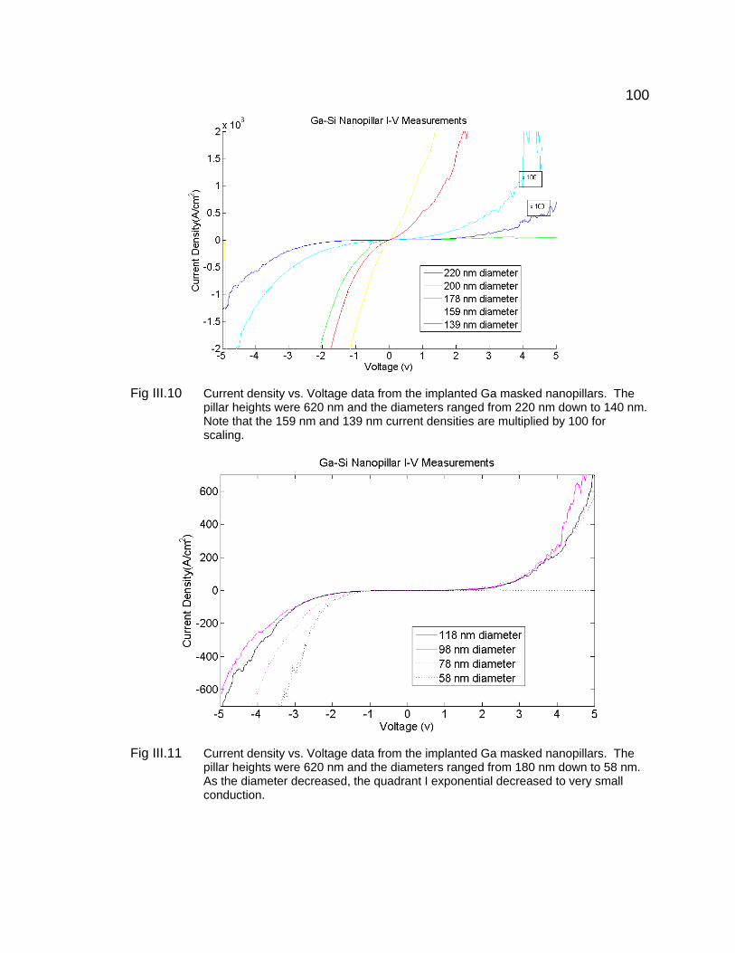
100
Fig III.10 Current density vs. Voltage data from the implanted Ga masked nanopillars. The
pillar heights were 620 nm and the diameters ranged from 220 nm down to 140 nm. Note that the 159 nm and 139 nm current densities are multiplied by 100 for scaling.
Fig III.11 Current density vs. Voltage data from the implanted Ga masked nanopillars. The
pillar heights were 620 nm and the diameters ranged from 180 nm down to 58 nm. As the diameter decreased, the quadrant I exponential decreased to very small conduction.

101 Finally, the last array measured consisted of 100 nm diameter pillars down to 40
nm diameters, and were decreased in 10 nm increments. The current densities measured
were approximately double that of what was measured in the 200 nm array. The
curvature was still the ‘s’ shaped symmetric exponential curves which became more non-
symmetric as the diameters decreased. The pillar diameters were also about 5-7 nm
larger in diameter than that written. Since the SEM resolution was not as high of quality as
that when using less magnification, an approximate error bar for the diameters would be
10 nm in diameter.
Fig III.12 Current density vs. Voltage data from the implanted Ga masked nanopillars. The
pillar heights were 620 nm and the diameters ranged from 110 nm down to 44 nm. As the diameter decreased, the quadrant I exponential decreased to very small conduction.
102
Electrical Properties of Vertical Nanopillars
Electrical conduction of semiconductors under reduced dimensions is becoming more
interesting and more important yearly as industry drives the transistor node downwards.
Current investigations in the nanoscale are displaying semiconductor physics that is much
different than what is seen on the micron scale. Importantly, conduction through long
(approximately 1 micron) and thin nanowires are of great concern as the semiconductor
electronics industry begins to launch fabrication lines at these scales. By looking at
conduction properties of both the alumina and the Ga masked silicon nanowires, this
section will detail observations and some conclusions made from in situ measurements
characterizing these devices by this relatively new method of measuring.
As was noted in previous sections, although several I-V and J-V curve shapes were
observed, two major classifications were devised. The first is a linear, or purely a resistive,
curve. This was more typically seen in the structures with areas bigger than 4*10-14 m2.
As the sizes reduced, a more general ‘s’ shaped curvature was seen. This regime was
further subdivided into symmetric and non-symmetric. Throughout this work, I-V curves
were typically displayed since their curvature includes the effect their area has on current
conduction. Larger areas typically display higher current magnitudes than smaller values.
For this reason, J-V curves are used to visually remove the magnitude effect in the plots
caused by the area. However, simply taking out the area from the saturation current does
not completely eliminate this effect. Evidence of this fact is obvious since the J-V curves
do not lie on top of each other. Since the nanopillars are small, typically only 2-probe
measurements are available for vertical pillars. The consequences of this measurement
restriction imply that the voltage driving the nanopillar is now distributed across the

103 contacting junction, the nanopillar, and the substrate/contact. Although the substrate
can be typically ignored, separation of the contact resistance and pillar resistance become
difficult. Even under the best of circumstances, the series resistance from the pillar can
act as a negative feedback on the contacting junction. Numerically separating this effect
becomes difficult, as the equation is transcendental, and plotting tends to require lots of
data manipulation beforehand.
A second effect involving area is that surface states are understood to create a
depletion region between the surface and bulk. This effect was introduced at the
beginning of this chapter and several publications made on this topic within the last few
years. Inclusion of this effect must be taken with care, however, since a simple
modification of saturation current (or current density) does not completely describe this
effect. Decreasing the diameter also increases the contact resistance. Further, although
the pillar becomes depleted of carriers, space-charge-limited current (SCLI) can dominate
conduction complicating standard assumptions of conduction in the depletion region.
Most measurements made to detail these types of measurements rely on knocking the
nanopillars over, lithographically constructing large metal contacts, and making 4 probe
measurements to eliminate these surface effects. The work performed for this thesis was
to explore the feasibility of in situ measurements. So the measurements here are
burdened with a 2-probe regime. Under the most difficult conditions, here a 40 nm
diameter pillar, it is possible to have the majority of the voltage applied, dropped across
the contact. This implies that measurements are describing junction effects instead of the
assumed pillar effects. As an example consider the best contacting situation, a highly

104 conductive tunnel contact. Then the measurement is actually a voltage divider
between the contact and the pillar resistance is as follows:
𝑉𝑉𝐽𝐽𝑠𝑠𝐿𝐿𝑐𝑐𝑑𝑑𝑐𝑐𝑐𝑐𝐿𝐿 = 𝑉𝑉𝜇𝜇𝑚𝑚𝑎𝑎𝑠𝑠𝑠𝑠𝑐𝑐𝑚𝑚𝑃𝑃 ∙ 𝑅𝑅𝐶𝐶𝑐𝑐𝐿𝐿𝑑𝑑𝑎𝑎𝑐𝑐𝑑𝑑
𝑅𝑅𝐶𝐶𝑐𝑐𝐿𝐿𝑑𝑑𝑎𝑎𝑐𝑐𝑑𝑑 +𝑅𝑅𝑃𝑃𝑐𝑐𝑠𝑠𝑠𝑠𝑎𝑎𝑐𝑐 = 𝑅𝑅𝐶𝐶𝑅𝑅𝐶𝐶+ 𝜌𝜌𝐿𝐿
1−2𝑁𝑁𝑠𝑠𝑐𝑐𝑁𝑁𝑎𝑎
Here, Rc is the specific contact resistance in Ohm-m2. Notice that device area is not a
factor here. For a reasonable barrier height and high doping, where tunneling is dominant,
one can expect a 10-3 Ohm-cm2 specific contact resistance. Given a 0.05 Ohm-cm
resistivity and 1 micron pillar height, the majority of the voltage is across the contact.
However, since contact resistance is only determined around zero volts, this is not always
the case. As the bias is increased, the device current increases exponentially and the
contact can rapidly become less resistive. However, measuring the slope of an I-V curve
around zero can provide insight on the behavior of the contacting junction.
Fig III.13 Contact resistance for pillars contacted directly by the tungsten probe tip and for
pillars with an a-Si Ga interface between the silicon and tungsten probe. The black line shows thermionic field emission theory for a 0.7 V barrier height.

105 By measuring both types of nanopillars in the manner described, the behavior of
the contact around zero was extracted. From the graph, measurements of the alumina
masked pillars (note the alumina was removed) and the Ga masked pillars display two
different behaviors. Since the alumina masked pillars effectively had the probe tip making
contact directly with the silicon, and the silicon was highly doped, it was expected that the
contact should be described by a thermionic-tunneling Schottky contact. Qualitatively,
although the barrier height is determined by the difference between the work function of
the metal and the work function of the silicon, the depletion width is controlled by the
doping levels. Using a 2*1019 cm-3 doping establishes a very thin depletion region, less
than 6 nm. At this thickness, tunneling can occur as described by Padovani et al [41].
However, the thermal energy is still a significant contribution to majority carrier conduction
over the barrier. For this reason, thermionic-field emission was used to describe the
barrier; this is the solid line in the figure.
𝑅𝑅𝑐𝑐 =𝑉𝑉𝑑𝑑ℎ ∙ 𝑉𝑉𝑐𝑐𝑐𝑐 ∙ 𝐶𝐶𝑐𝑐𝑠𝑠ℎ
𝑉𝑉𝑐𝑐𝑐𝑐𝑉𝑉𝑑𝑑ℎ 𝐶𝐶𝑐𝑐𝑑𝑑ℎ 𝑉𝑉𝑐𝑐𝑐𝑐 𝑉𝑉𝑑𝑑ℎ
𝑑𝑑∗∗𝑇𝑇2𝜋𝜋𝜙𝜙𝐵𝐵𝑠𝑠 − 𝜙𝜙𝑠𝑠∙ 𝐸𝐸𝐸𝐸𝑠𝑠
𝜙𝜙𝐵𝐵𝑠𝑠 − 𝜙𝜙𝑠𝑠𝑉𝑉𝑐𝑐𝑐𝑐𝐶𝐶𝑐𝑐𝑑𝑑ℎ
𝑉𝑉𝑐𝑐𝑐𝑐𝑉𝑉𝑑𝑑ℎ
−𝜙𝜙𝑠𝑠𝑉𝑉𝑑𝑑ℎ
𝑤𝑤ℎ𝑚𝑚𝑐𝑐𝑚𝑚 𝑉𝑉𝑐𝑐𝑐𝑐 =ℏ2
𝑁𝑁𝑑𝑑𝜇𝜇∗𝜖𝜖𝑠𝑠𝑐𝑐
Here, Vth is the thermal voltage of 0.02582 V, φBp and φp are the barrier height and the
difference between Fermi level and valence band respectively, Voo is approximated at 22.6
mV, A** is the Richardson constant, and T is the temperature. The barrier height is
approximated at 0. 7 V for a p-type silicon and tungsten contact.
A striking difference was observed for the W/a-Si Ga/Si contact. Large areas show a
significantly reduced barrier potential. This was commented on previously when micro-

106 Amps were measurable on the square pillars vice the tungsten contacted pillars
showing pA. Even more striking is the transition from the low contact resistance to that of
where a contact barrier of 0.7 V is seen. The 100 – 40 nm Ga pillar array shows a high
contact barrier. The 500 – 150 nm Ga pillar array shows a very low contact barrier. The
200 – 40 nm barriers shows the transition range with satisfactory overlap between the two
barriers.
The reduced contact resistance in the 500-200 nm range can be explained by
approximating the effect as a graded junction. It is likely that with the a-Si Ga interface
acting as a highly doped, thin silicon region a reduced barrier height is achieved [42].
Fig III.14 Illustration of a possible method for the reduction of the contact barrier when using
implanted Ga etch masks. It was observed that the implantation reduces contact barrier height from 0.7 V to 0.26 V.
∆𝜙𝜙𝐵𝐵𝑠𝑠~𝑞𝑞𝜖𝜖𝑠𝑠𝑐𝑐
∙ 𝑁𝑁𝐺𝐺𝑎𝑎∙𝑑𝑑𝐺𝐺𝑎𝑎
4𝜋𝜋
Here, tGa is the remaining thickness of the mask and NGa is approximated doping. By
making very modest assumptions of doping of the Ga mask at 5*1019 cm-3 with a thickness
of 20 nm, a theoretical barrier height reduction of 0.44 V occurs. By reducing the barrier
height to 0.2 V, thermionic tunnel theory predicts a significant resistance reduction. This

107 effect is striking since anneals are typically required to activate the implantation;
although it is known that implantation does activate some of the ions due to heating.
Fig III.15 Contact resistance for pillars contacted directly by the tungsten probe tip and for
pillars with a-Si Ga interface between the silicon and tungsten probe. The lines shows thermionic field emission theory for a 0.7 V barrier height (dotted) and 0.26 V reduced barrier height (solid).
The 200 – 40 nm nanopillar range provides a striking transition from the low barrier
height to the expected Schottky barrier height. Although what is physically happening
during the transition is enigmatic, it is clear that the effective barrier height (φBp-∆φBp-φp)
term is responsible. With the W Si nanopillars below 100 nm diameter, the contact
resistance is only slightly greater than that expected from the larger pillars. Since the
barrier height reduction is not applicable, the (φBp -φp) difference is what is responsible for
this slight increase. Feasible increases in this effective barrier height of 0.1 – 0.2 V
numerically describe the data. The a-Si Ga nanopillars demonstrate a diameter
dependent increase in barrier height with a rate of approximately 0.6 V per 100 nm. This
dependence stops around 100 nm where the barrier height returns to the 0.7 V regime. It
is likely that surface states, either from the sides of the pillar or between the metal silicon
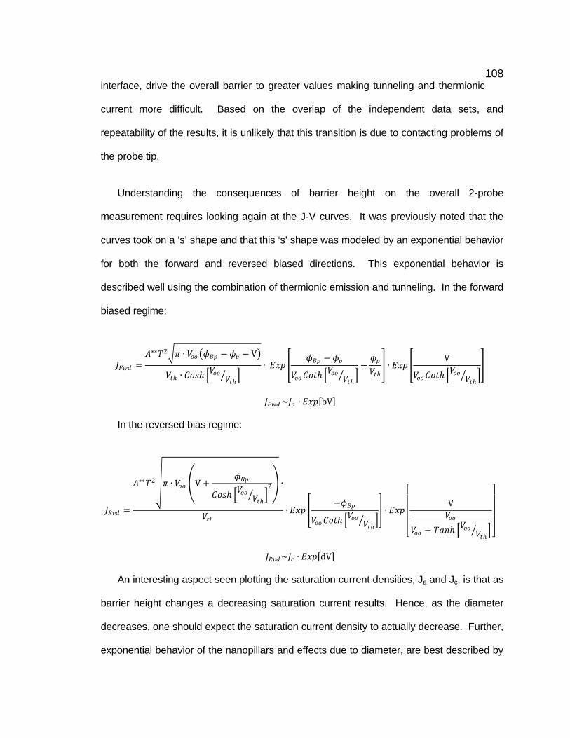
108 interface, drive the overall barrier to greater values making tunneling and thermionic
current more difficult. Based on the overlap of the independent data sets, and
repeatability of the results, it is unlikely that this transition is due to contacting problems of
the probe tip.
Understanding the consequences of barrier height on the overall 2-probe
measurement requires looking again at the J-V curves. It was previously noted that the
curves took on a ‘s’ shape and that this ‘s’ shape was modeled by an exponential behavior
for both the forward and reversed biased directions. This exponential behavior is
described well using the combination of thermionic emission and tunneling. In the forward
biased regime:
𝐽𝐽𝐹𝐹𝑤𝑤𝑃𝑃 =𝑑𝑑∗∗𝑇𝑇2𝜋𝜋 ∙ 𝑉𝑉𝑐𝑐𝑐𝑐 𝜙𝜙𝐵𝐵𝑠𝑠 − 𝜙𝜙𝑠𝑠 − V
𝑉𝑉𝑑𝑑ℎ ∙ 𝐶𝐶𝑐𝑐𝑠𝑠ℎ 𝑉𝑉𝑐𝑐𝑐𝑐
𝑉𝑉𝑑𝑑ℎ ∙ 𝐸𝐸𝐸𝐸𝑠𝑠
𝜙𝜙𝐵𝐵𝑠𝑠 − 𝜙𝜙𝑠𝑠𝑉𝑉𝑐𝑐𝑐𝑐𝐶𝐶𝑐𝑐𝑑𝑑ℎ
𝑉𝑉𝑐𝑐𝑐𝑐𝑉𝑉𝑑𝑑ℎ
−𝜙𝜙𝑠𝑠𝑉𝑉𝑑𝑑ℎ
∙ 𝐸𝐸𝐸𝐸𝑠𝑠 V
𝑉𝑉𝑐𝑐𝑐𝑐𝐶𝐶𝑐𝑐𝑑𝑑ℎ 𝑉𝑉𝑐𝑐𝑐𝑐
𝑉𝑉𝑑𝑑ℎ
𝐽𝐽𝐹𝐹𝑤𝑤𝑃𝑃 ~𝐽𝐽𝑎𝑎 ∙ 𝐸𝐸𝐸𝐸𝑠𝑠[bV]
In the reversed bias regime:
𝐽𝐽𝑅𝑅𝑅𝑅𝑃𝑃 =
𝑑𝑑∗∗𝑇𝑇2𝜋𝜋 ∙ 𝑉𝑉𝑐𝑐𝑐𝑐 V +𝜙𝜙𝐵𝐵𝑠𝑠
𝐶𝐶𝑐𝑐𝑠𝑠ℎ 𝑉𝑉𝑐𝑐𝑐𝑐 𝑉𝑉𝑑𝑑ℎ 2 ∙
𝑉𝑉𝑑𝑑ℎ∙ 𝐸𝐸𝐸𝐸𝑠𝑠
−𝜙𝜙𝐵𝐵𝑠𝑠𝑉𝑉𝑐𝑐𝑐𝑐𝐶𝐶𝑐𝑐𝑑𝑑ℎ
𝑉𝑉𝑐𝑐𝑐𝑐𝑉𝑉𝑑𝑑ℎ
∙ 𝐸𝐸𝐸𝐸𝑠𝑠
⎣⎢⎢⎢⎡
V𝑉𝑉𝑐𝑐𝑐𝑐
𝑉𝑉𝑐𝑐𝑐𝑐 − 𝑇𝑇𝑎𝑎𝐿𝐿ℎ 𝑉𝑉𝑐𝑐𝑐𝑐 𝑉𝑉𝑑𝑑ℎ ⎦⎥⎥⎥⎤
𝐽𝐽𝑅𝑅𝑅𝑅𝑃𝑃~𝐽𝐽𝑐𝑐 ∙ 𝐸𝐸𝐸𝐸𝑠𝑠[dV]
An interesting aspect seen plotting the saturation current densities, Ja and Jc, is that as
barrier height changes a decreasing saturation current results. Hence, as the diameter
decreases, one should expect the saturation current density to actually decrease. Further,
exponential behavior of the nanopillars and effects due to diameter, are best described by

109 the contact vice the nanowire itself. This conclusion explains a fair amount of the
results seen across the scientific community. Similar effects were seen from both the W Si
contacts and the W a-Si/Ga Si contacts. To demonstrate this point, the curve fitted
parameters from the 200 – 40 a-Si/Ga nanopillars was tabulated for all the coefficients and
R2 values. It is interesting to note that there is a slight difference in Ja and Jc values.
Fig III.16 Theoretical saturation current densities, Ja and Jc, reducing as barrier height
increases, as predicted from thermionic field emission theory. The values used are the same as stated earlier in this section. The forward bias, Ja, is constantly a smaller than Jb for the same barrier.
Fig III.17
Pillar Diameter (nm) Ja b Jc c R2 200 1.84E+09 1.039 -1.78E+09 -1.388 0.9988 180 3.29E+09 1.512 -3.33E+09 -1.655 0.9993 160 - - -1.60E+08 -3.372 0.9675 140 6.77E+05 2.014 -7.23E+05 -2.086 0.9985 120 1.45E+04 3.347 -1.46E+04 -3.494 0.9930 100 4.67E+03 1.681 -6.34E+03 -1.734 0.9976
80 2.49E+03 1.883 -8.09E+03 -1.632 0.9969 60 2.83E+03 2.154 -2.20E+03 -2.668 0.9903 40 - - -4.87E+03 -2.477 0.9776
0.2 0.3 0.4 0.5 0.6 0.7Bp
104
106
108
1010Ji

110 Hence, thermionic field emission in both the forward and reversed biased regimes
gives a good description of the presented nanowires. The nanowires were seen to have
exponential current behavior in quadrant 1 and 3 which can be closely modeled by I =
Ia*Exp(b*V) + Ic*Exp(d*V). Using the amorphous silicon with implanted Ga yields a highly
conductive interface which acts as a gradient doped silicon – metal interface. This
interface, on the hundreds of nanometer scales, yields a reduced barrier potential allowing
for a significantly reduced contact resistance. As the diameter decreases from 200 to 100
nm, a transition was observed. It is likely that this transition, described as an increasing
barrier potential, is due to a depletion of charge carriers or potentially from surface states.
Using a 2-probe measurement system also was shown to describe more of the physics of
the interface, or contact resistance, rather than the pillar itself. In order to efficiently use
the nanopillars for sensors, contact resistance will need to be reduced to below that of the
pillar resistance. Although further investigation of the contact resistance transition is
needed, implanted Ga in silicon seems to offer an advantageous method for probing
silicon nanowires.
Lateral Ga-Silicon Nanowires / Nanobeams
Vertical silicon nanowires and silicon nanopillars offer the ability to expand silicon
technology out of the classic lateral plane. However, there are still technologies which
utilize silicon nanowires laterally. Such technologies are lateral electrical wire runs and
lateral mechanical beams. It was demonstrated that lateral wires could be fabricated
using the implanted gallium mask and that this technology could even be multiplanar;
demonstrated by placing the wire 1 micron below the surface. This technology was
expanded to two extremes; the fabrication of nanoscale reduced dimensions and wide
lateral beams.
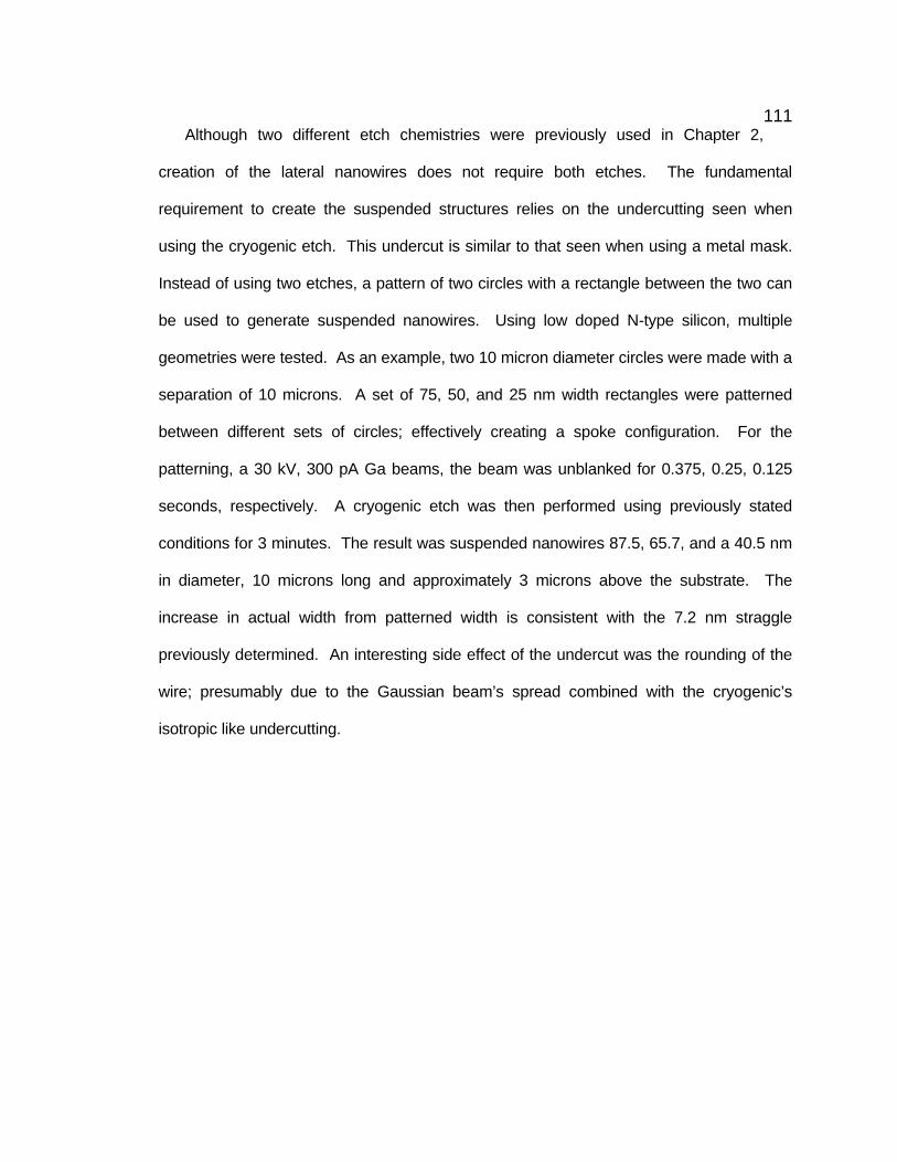
111 Although two different etch chemistries were previously used in Chapter 2,
creation of the lateral nanowires does not require both etches. The fundamental
requirement to create the suspended structures relies on the undercutting seen when
using the cryogenic etch. This undercut is similar to that seen when using a metal mask.
Instead of using two etches, a pattern of two circles with a rectangle between the two can
be used to generate suspended nanowires. Using low doped N-type silicon, multiple
geometries were tested. As an example, two 10 micron diameter circles were made with a
separation of 10 microns. A set of 75, 50, and 25 nm width rectangles were patterned
between different sets of circles; effectively creating a spoke configuration. For the
patterning, a 30 kV, 300 pA Ga beams, the beam was unblanked for 0.375, 0.25, 0.125
seconds, respectively. A cryogenic etch was then performed using previously stated
conditions for 3 minutes. The result was suspended nanowires 87.5, 65.7, and a 40.5 nm
in diameter, 10 microns long and approximately 3 microns above the substrate. The
increase in actual width from patterned width is consistent with the 7.2 nm straggle
previously determined. An interesting side effect of the undercut was the rounding of the
wire; presumably due to the Gaussian beam’s spread combined with the cryogenic’s
isotropic like undercutting.

112
Fig III.18 Scanning electron micrograph of Ga implanted Si nanowires 10 microns long and
suspended 3 microns high. The nanowire diameters intended were 75, 50, and 25 nm. Top left shows a 87.5 nm wire, top right and bottom left show a 65.7 nm wire, and bottom right shows a 40.5 nm wire.
Fig III.19 Scanning electron micrograph of Ga implanted Si nanowires 40 nm in diameter and
16 microns long.

113 In a second experiment, a 25 nm by 16 micron rectangle situated between two 3
micron diameter circles was Ga patterned and etched yielding a 40 nm diameter beam 16
microns long. Although these devices demonstrate the wide application of the implanted
Ga etch masking, an important feature of this technique should be reiterated. These
silicon nanowires are actually amorphous silicon with some Ga bonded, probably activated
during the implantation, and some Ga left interstitially. Reflection electron microscopy in
the TEM, similar to that performed on the nanopillars, was performed on these lateral
nanowires. This verified that the nanowires were amorphous and the body of the micron
post remained crystalline. Since the pillars were wide and the resistance to the substrate
very small, it presented a technical difficulty in measuring the electrical resistance of the
nanowires.
Fig III.20 Transmission electron micrograph of Ga implanted Si nanowires 40 nm in diameter
and 10 microns long.

114 To address the multiple electrical conduction paths, much larger scale devices
were fabricated on SOI (silicon on insulator). The top layer of silicon was N-type 37.5-62.5
ohm-cm silicon 1 micron thick on 1.5 micron thick silicon dioxide. The low resistivity of the
top silicon layer implies a very low doping of 1014 cm-3. By etching the structure in the top
silicon layer, down to the oxide layer, conductivity could be ensured to be through the
lateral wire. For this experiment, much thicker silicon beams were designed. The
patterned beams were originally 50, 75, and 100 nm wide and 10 microns long, situated
between 10 micron diameter pillars. Implantation in the FEI Nova 200 was performed
using a 30kV and 290 pA beam. The areal doses of the beams were 1.45*1017 cm-2,
1.21*1017 cm-2, and 1.45*1017 cm-2 for the 50, 75, and 100 nm beams respectively. The
silicon was cryogenically etched in the ICP-380 machine for 80 seconds under the
following conditions:
SF6 70 sccm ICP Power 900 W
O2 4 sccm Fwd Power 3 W
Temperature -130 C Pressure 10 mt
The etch was tuned to undercut less than 1 micron; this permitted the silicon
micropillar to remain mostly vertical but allowed for the beam to be completely undercut
and freed. Since the Fwd power was tuned down and a cryogenic etch used, the
selectivity of the Ga etch mask significantly increased the width of the beam. This etch
tuning combined with the beam being slightly defocused resulted in final beam dimensions
of 142 nm, 194 nm, and 252 nm widths. The length was measured to 10 microns and the
thickness of the beams approximated to 25 nm based on the implantation straggle. For
this experiment, each set of 3 beams was written 3 times to make a total of 9 beams. This
redundancy was used to verify resistance measurements taken. The total write time for a

115 set of beams was approximately 4.5 minutes three beams and the etch time was 1.3
minutes. Including sample loading and unloading from vacuum chambers, the total time to
fabricate silicon nanobeams was under 20 minutes and did not require wet chemicals at
any stage.
Fig III.21 SEM of 2 tungsten probe tips contacting one of three lateral Ga-Si beams 10
microns long. The I-V measurements of these beam indicates a resistivity improvement from 40 to ~1 Ω-cm.
With the fabrication completed, the samples were loaded onto the probe stage in the
Quanta SEM. Two tungsten probe tips were brought down to make contact on the two 10
micron diameter pads. Several preliminary measurements were made to verify that there
were no alternate conduction paths other than going through the beam: both probes
contacting the substrate measured as an open circuit, and one pillar on a pad and the
other left dangling measured an open circuit. Given the dimensions of the beams and the
lowest resistivity of the crystalline silicon, expected resistances should be 1.056 GΩ, 773

116 MΩ, and 595 MΩ respectively. Actual measurements yielded resistances around 100
MΩ and down to 14 MΩ. Given the physical dimensions of the beams, an upward bound
of the resistivity of the beams were measured to 0.2-4.5 Ohm-cm. The measurements
were repeated over each of the three groups and then performed again on an identically
fabricated second sample. All of the measurements were within the range reported here.
Although the exact nature of the conductivity is not understood in detail, qualitatively the
interstitial Ga mixed with amorphous silicon creates a type of binary phase material. It is
likely that the conduction of this sludge-like layer is mostly due to the conduction through
the Ga.
Fig III.22 Current vs. Voltage measurements of implanted Ga masked lateral silicon
nanobeams. From the geometry, resistivity of less than 5 Ohm-cm was inferred. The red curves was for a ~150 nm wide beam, the green curve was for a ~200 nm wide beam, and the blue curve for a ~250 nm wide beam.
Several observations were made during the probing of the beams. First, the SEMs
denote a clear differentiation of the Ga implanted silicon and the crystalline silicon. This is
seen from changes in SEM signal intensity of the 10 micron pad. The images are seen as
bright discs atop of a darker etched structure. The undercut of the disc also denotes this
transition. Second, in many of the high areal dosed Ga implanted regions, there are dots
of brighter intensity. This feature is notable, for example, in the 40 nm diameter nanowires

117 and in the 10 micron contact pads. TRIM calculations indicate that an aerial dose of
1*1017 cm-2 results in a maximum Ga density of 4*1022 cm-3; this is exceeding the solid
solubility of Ga in silicon at room temperature [43]. It is likely that these dots are locations
where the Ga segregate and coalesce from the amorphous silicon [44]. This segregation
was not seen for the lower dose, such as with the critical dose array described in Chapter
2. Some future experiments might include TEMs of the dose array to determine when the
segregation begins. Since the lower areal dose limit is based on the selectivity from the
etch, this segregation dynamics might act as the upper limit for areal doses instead of the
milling limit.
Fig III.23 SEM of a lateral implanted Ga masked silicon nanobeam. The beam was
constructed on SOI with a 1 micron thick silicon layer. Note the bright regions on both the beam and the pad which is interpreted as Ga segregating out of the etch mask due to a high areal dose.
A third observation made was that during the probing of the pads, the amorphous
silicon – gallium layer was able to be physically moved about using the tungsten probe tip.

118 Further, if the probe tip was pushed down too far, the tungsten could make contact
with the low doped silicon and greatly increase the resistance measured. This layer is
likened to mud, where it the combination of sand and water creates a dual phase system.
In this case, the Ga would act as the liquid state and the amorphous silicon as the solid
state. From this idea, it was hypothesized that annealing could recrystallize the silicon
while activating the Ga (placing the Ga in the diamond lattice structure of the silicon). As a
first attempt, a 12 hour N2 anneal at 1000 C was performed on the samples. Resulting
from the temperature changes, all of the beams were fractured; the appearance of the
broken beams indicates that they were under tensile stress. Most importantly, sections of
the contact pad could be fractured off and all of the observed Ga segregations were no
longer present. From many sessions probing these implanted structures, fracturing of
unannealed sections has not been observed. These observations are encouraging and
future work might include optimizing anneal for these nanobeams; possibly to
independently control Ga activation and recrystallization. It was also hypothesized that a
Rapid Thermal Anneal before etching could heal the silicon and activate the Ga. For this
experiment, the RTA was performed at 800C for 2 minutes. Optically, it was observed that
the Ga segregations remained, indicating that a significant amount of Ga diffusion did not
occur. However, under identical etching conditions to that which fabricated the
nanobeams described earlier, there was no masking effect on the silicon except where the
Ga segregations were observed. Although not conclusive, it is likely that some of the
implanted Ga did activate, leaving little interstitial Ga. This might have prevented the
bonding of F or O to the Ga to act as an etch mask.
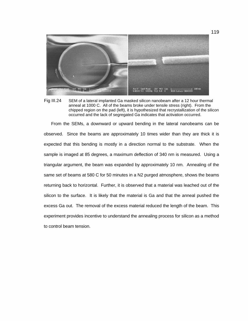
119
Fig III.24 SEM of a lateral implanted Ga masked silicon nanobeam after a 12 hour thermal
anneal at 1000 C. All of the beams broke under tensile stress (right). From the chipped region on the pad (left), it is hypothesized that recrystallization of the silicon occurred and the lack of segregated Ga indicates that activation occurred.
From the SEMs, a downward or upward bending in the lateral nanobeams can be
observed. Since the beams are approximately 10 times wider than they are thick it is
expected that this bending is mostly in a direction normal to the substrate. When the
sample is imaged at 85 degrees, a maximum deflection of 340 nm is measured. Using a
triangular argument, the beam was expanded by approximately 10 nm. Annealing of the
same set of beams at 580 C for 50 minutes in a N2 purged atmosphere, shows the beams
returning back to horizontal. Further, it is observed that a material was leached out of the
silicon to the surface. It is likely that the material is Ga and that the anneal pushed the
excess Ga out. The removal of the excess material reduced the length of the beam. This
experiment provides incentive to understand the annealing process for silicon as a method
to control beam tension.

120
Fig III.25 SEMs of a lateral implanted Ga masked silicon nanobeam before (left) and after
(right) a 50 minute thermal anneal at 580 C. Comparison of the two SEMs indicate that the beam was laterally extended by 10 nm and upon annealing, the material forcing the extension is pushed to the surface returning the beam to horizontal.

121 C h a p t e r I V
Micrometer Scaled Devices This chapter details applications of the etching and fabrication developed for micron length
scales. There are two major applications of this work in silicon and they will be discussed
separately. The first application was the push to develop portable nuclear magnetic
resonance (NMR) integrated into silicon. For this application, several devices were
created: a 1 Tesla magnetic field created using NdFeB permanent magnets, and planar
microcoils in silicon. The magnetic field was shimmed by fabrication of high susceptibility
iron shims in silicon and placed on the surface of the permanent magnet. The planar
microcoils were also fabricated in silicon for use as RF magnetic field pulsing to a sample
volume and then for detection of the oscillating magnetic fields. Although the NMR
apparatus was not completed, a detailed description of the devices as well as
experimental evaluation will be discussed here. The second major application of the
micron scale work was fabrication of the silicon micropillars described earlier. Besides
their specific use in calibration and exploration of the cryogenic etch, these pillars were
used for photovoltaic experiments and electrical measurements of Schottky point diodes.
The purpose of the diode measurements was to provide understanding critical for the
nanowires and will be described in this chapter for completeness. In all of these projects,
the cryogenic etching of silicon was the enabling technology to achieve both the planar
iron shims and the planar microcoils.
Components of a Portable NMR Apparatus 1 Tesla Magnetic Field and Shimming
This section will detail the generation of the 1 Tesla (T) field using permanent
neodymium-iron-boron (NdFeB) magnets. Creation of the magnetic field began with the

122 design of the inhomogeneous magnetic field. The standard method of generating the
magnetic fields for NMR is to use cooled superconductive electromagnets. Fields
generated in this manner can exceed more than 20 T for volumes of several cubic
centimeters. Although the sensitivity of NMR is proportional to the square of the field, the
cost of these can be upwards of several hundred thousand dollars and occupy a very
large physical space. As an alternative, there has been interest in utilizing low field
permanent magnets due to their low cost and physical size [45,46,47]. The objective of
the design described here is to create a low cost, 1 T magnetic field, and using NdFeB
magnets in a portable setting so it does not consume any electrical power. Once the
magnetic field is established, the second goal was to make a homogenous magnetic field
over as large a volume as possible using passive shims [48]. Shims are usually a highly
susceptible magnetic material used to alter magnetic fields similar to how lenses can bend
light based on the material’s index of refraction [49,50]. To precisely fabricate the passive
shims, a design for iron deposited in lithographically patterned silicon was engineered.
To generate the 1 T field a simple magnetic circuit was designed. The geometry of the
design was set to minimize the inherent inhomogeneity while maximizing the magnitude of
magnetic field attainable [51]. An attractive geometry was chosen such that two of the
NdFeB magnets, separated by an air gap, were connected using magnetic steel; the so
called ‘C’ configuration. Due to the hysteresis of permanent magnets, the length and the
area of the air gap separating the magnets alters the strength of the magnetic field. To
determine the strength of the field, the magnetic field flux and magneto-motive force are
simultaneously solved [52]. The resulting magnet’s magnetic field dependence on the
auxiliary magnetic field, H, is then plotted on the magnet’s demagnetization curve to find
the air gap’s magnetic field. To begin, note that the magnetic field flux leaving the

123 magnet’s face is equal to the field flux entering the gap. Then calculate the
magnetomotive force over the steel loop, air gap and magnets. Substitution using the two
equations yields an equation for a straight line.
𝐵𝐵𝑔𝑔𝑎𝑎𝑠𝑠 ∗ 𝑑𝑑𝑔𝑔𝑎𝑎𝑠𝑠 = 𝐵𝐵𝜇𝜇𝑎𝑎𝑔𝑔 ∗ 𝑑𝑑𝜇𝜇𝑎𝑎𝑔𝑔
𝐻𝐻.𝑃𝑃𝑠𝑠 = 0 = 𝐻𝐻𝑔𝑔𝑎𝑎𝑠𝑠 ∗ 𝑠𝑠𝑔𝑔𝑎𝑎𝑠𝑠 + 2 ∗ 𝐻𝐻𝜇𝜇𝑎𝑎𝑔𝑔 ∗ 𝑠𝑠𝜇𝜇𝑎𝑎𝑔𝑔 + 𝐻𝐻𝑠𝑠𝑑𝑑𝑚𝑚𝑚𝑚𝑠𝑠 ∗ 𝑠𝑠𝑠𝑠𝑑𝑑𝑚𝑚𝑚𝑚𝑠𝑠
𝐵𝐵𝜇𝜇𝑎𝑎𝑔𝑔 = 𝐻𝐻𝜇𝜇𝑎𝑎𝑔𝑔 ∗
⎝
⎛−2𝜇𝜇𝑐𝑐
𝑠𝑠𝜇𝜇𝑎𝑎𝑔𝑔𝑠𝑠𝑔𝑔𝑎𝑎𝑠𝑠
𝑑𝑑𝑔𝑔𝑎𝑎𝑠𝑠𝑑𝑑𝜇𝜇𝑎𝑎𝑔𝑔
(1 + 𝑠𝑠𝑠𝑠𝑑𝑑𝑚𝑚𝑚𝑚𝑠𝑠𝜇𝜇𝑐𝑐−𝑠𝑠𝑑𝑑𝑚𝑚𝑚𝑚𝑠𝑠 ∗𝑠𝑠𝑔𝑔𝑎𝑎𝑠𝑠
𝑑𝑑𝑔𝑔𝑎𝑎𝑠𝑠𝑑𝑑𝑠𝑠𝑑𝑑𝑚𝑚𝑚𝑚𝑠𝑠
)⎠
⎞
Assuming the gap area and magnet area are matched, a numerical solution for a 2
inch diameter magnet yields a slope of -5.083/lgap in units of T/kOe; this assumes a very
large relative permeability of the steel. Placing this line, in red, in the demagnetization
curve for a N42 or N52 magnet allows for the determination of the magnetic field in the air
gap from the intersection of the two lines. Note that the demagnetization of the magnet
depends upon temperature. Further, multiple correction factors should be added to
account for non-idealities losses. However, once the slope is calculated for a given
system and a correction factor determined, it should be constant for any strength magnet
of similar dimensions. This calculation is most useful for considerations of magnet holder
geometry.

124
Fig IV.1 Demagnetization curves for KJ Magnetics NdFeB magnets of N42 and N52. The red
line is the theoretical demagnetization line; the intersection of the two lines indicate the magnetic field in the air gap.
Using the calculation described above, a holder was designed for 2 inch diameter, 1
inch thick NdFeB magnets. A Garolite fiberglass was constructed to maintain a magnet
separation, or air gap, of close to 6 mm. The Garolite holder was constructed of 4 pieces
so two magnets could be controllably brought together and placed in the steel loop.
Fig IV.2 Model of the NdFeB magnetic circuit. The blue represents the steel loop and the
brown represents the Garolite holders.

125 Precise control over the magnet was incredibly important because of magnet’s
strength. Placing two magnets in contact would require 232 lbs-force for N42 and 278 lbs-
force for N52 to separate them again. To safely construct the magnetic circuit the
following sequence would need to be performed: 1) lock a single magnet between two
holders, 2) slowing bring a vertical steel bar into contact with the backside of the magnet,
3) repeat steps 1 and 2 on the second magnet, 4) slowly bring the two magnets together
until the Garolite holders make contact with each other, 5) slowly bring the horizontal steel
bar into contact with the two vertical steel bars. Once completely assembled, the magnet
is held together with the majority of the magnetic field trapped in the steel loops and
magnets or in the air gap. Typical measurements of the field just outside of the gap were
approximately 5 Gauss (ten times the Earth’s magnetic field).
Fig IV.3 Picture of the NdFeB magnetic circuit mounted in the apparatus which slowly brings
the magnets together. All of the frame was constructed from non-ferromagnetic materials.
Using Comsol and FEMM (both are a finite element magnetic solvers) the magnetic
fields were simulated. Simulations were performed in 2-D utilizing symmetry of the system
in both cylindrical and Cartesian coordinates. The cylindrical simulations placed the r=0

126 axis along the center line of the magnets and the z axis along the direction of the
magnetic field. This assumes symmetry along the theta axis which is not completely valid;
this simulated configuration would have the iron loop completely encasing the Garolite
holder. To correct for this, simulations in a Cartesian coordinate system were used. In
fact the magnetic field across the center of the gap demonstrated a slight perturbation due
to the fact that the iron holder was present. This perturbation will be discussed later. To
model the magnets, several different terms were required, the relative permeability (µr),
the electrical conductivity (σ), the residual flux density (Br), and the coercive force (Hc).
The conductivity was 0.667 MS/m. The residual flux density and coercive force for the
N42 was 1.32 T and 875,820 A/m and for the N52 was 1.48 T and 891,744 A/m. These
values were suggested by the manufacturer, KJ Magnetics (www.kjmagnetis.com).
Fig IV.4 Comsol simulation for determination of the magnetic field. The pink sections contain
the magnetic flux, the steel loop and the magnets. The white field is simulated as free space.

127 Running simulations of the magnetic field allowed for the field homogeneity to be
determined. Typically, plots of the Bz field plotted both radial at z=0 (center of the air gap)
and azimuthally at r=0 (along the center of the magnet) were used for characterization of
the homogeneity defined here as (Bzmax –Bzmin)/( Bzmax) over a specified radial or azimuthal
distance. Unshimmed, the magnetic homogeneity was simulated in Comsol as 5273 ppm
over a 1 cm diameter radially and 3568 ppm over the 6 mm azimuthal gap. Simulation of
FEMM in radial coordinates yields a radial homogeneity of 4661 ppm and an azimuthal
homogeneity of 2777 ppm. This level of inhomogeneity is unacceptable for conducting
proton NMR experiments and requires shimming [48,53].
Fig IV.5 Simulation for determination of the magnetic field homogeneity. The top graph
depicts the magnetic field, Bz, plotted radially at the center of the air gap. The bottom graph shows Bz plotted azimuthally along r=0.
To verify the calculations and simulations, the magnetic field was measured using a
LakeShore Model 455 single axis Gauss meter. The Hall probe was mounted on a 3
stage micrometer and zeroed. Placement of the micrometer was measured using a
caliper to be approximately square and the setup was measured on a wooden table (glued
together) to minimize field distortions due to metal ferromagnetic objects. To ensure the
probe’s surface was normal to the magnetic field, the probe was rotated to reach a

128 maximum field reading. Centering of the micrometer was an iterative process where
the radial maxima was first determined in two directions (radial) then the minima was
located azimuthally. This process would repeat 3 to 4 times until variations of the peak
field were smaller than 10 µT. The micrometer was moved in 500 (250 for azimuthal)
micron increments noting the temperature of the probe. Typical measurements were
conducted slowly, taking approximately 10 minutes, to prevent temperature fluctuations of
the Hall probe. Using Matlab’s curve fitting toolbox, the measured data was numerically
fitted to solve for two components: coefficient for a parabolic curvature, and lateral offset of
the field maxima. The maximum magnetic field was set at the highest value
experimentally recorded. Due to the cylindrical symmetry of the magnetic field, a negative
parabolic function was assumed. From the curve fitting, a lateral offset from zero of
approximately 900 microns was seen with a 3558 ppm radial homogeneity over a 1 cm
diameter.
Fig IV.6 Gaussmeter measurement of the magnetic field homogeneity. The top graph depicts
the magnetic field, Bz, plotted radially at the center of the air gap. The bottom graph shows Bz plotted azimuthally along r=0. Data points are marked with an ‘x’.
A second experiment was performed to determine the magnetic field’s dependence on
the air gap length. For this experiment, the magnets were separated in measured 1 mm
increments. Upon separation, the magnetic field’s center was again determined using the

129 Gaussmeter mounted on the micrometers to determine the azimuthal minima and
radial maxima. As a second check of the length, the azimuthal micrometer was used to
verify that the minima shifted only 0.5 mm. The data was plotted along with the FEMM
simulated data and fitted to 1/(1+x) curves. The basis for using this function derives from
using the air gap equation and approximating the demagnetization curve as linear.
𝐵𝐵𝜇𝜇𝑎𝑎𝑔𝑔𝐿𝐿𝑚𝑚𝑑𝑑 = 𝜇𝜇𝑐𝑐(1 + 𝜒𝜒)𝐻𝐻𝜇𝜇𝑎𝑎𝑔𝑔𝐿𝐿𝑚𝑚𝑑𝑑 + 𝐵𝐵𝑐𝑐 𝑎𝑎𝐿𝐿𝑃𝑃 𝐵𝐵𝑔𝑔𝑎𝑎𝑠𝑠 = −2𝜇𝜇𝑐𝑐𝑠𝑠𝜇𝜇𝑠𝑠𝑔𝑔𝑎𝑎𝑠𝑠
𝐻𝐻
Where Br is the residual magnetic field of the magnet, typically quoted by the vendors,
lm is the length of the magnet, lgap is the length of the air gap and χ is the susceptibility of
the magnet. The intersection of these two equations on the demagnetization curve occurs
when the H fields are matched. This yields the following dependence on the air gap
length:
𝐵𝐵𝑔𝑔𝑎𝑎𝑠𝑠 =𝐵𝐵𝑐𝑐
(1 + 𝜇𝜇𝑐𝑐2𝑠𝑠𝑔𝑔𝑎𝑎𝑠𝑠𝑠𝑠𝜇𝜇
)
Under the assumption that the magnet’s length is 25.4 mm, the measured residual
magnetic field was determined to be 1.363 T and the magnets relative permeability of
1.911 to an r-square value of 0.9975. Note that magnetic losses are typically represented
by a factor multiplied by the ratio of the lengths. Unfortunately, this factor and the
permeability term are inseparable; so the 1.911 was really a composite of the terms and
should not be thought of as the actual permeability. The determination of the residual
magnetic field, allowed for more precise simulations by using this value when describing
the simulated magnets. Although adjusting the simulated magnets’ residual magnetic field
helped, comparison of the new simulated results with experiments still shows that that the
simulated field decreases slightly faster as the air gap is increased.

130
Fig IV.7 Simulation (blue circles) and measurement (red x) of Bz field as the air gap was
increased. The measurement was made using a LakeShore 455 Gaussmeter with the Hall probe mounted on a micrometer. The arrows show the change in simulations results as the magnets are adjusted from supplier’s characteristics to the measured Br.
The large inhomogeneity demonstrated is unacceptable for proton NMR experiments.
Magnetic field broadening decreases the NMR’s peak signal intensity by spreading the
number of signal generators out over a wider frequency range. Field homogeneity should
be as uniform as possible over as large a volume as possible. To perturb the field towards
more homogeneity, devices referred to as shims are utilized. Shims can either be (and
typically are) active electromagnets or passive ferromagnetic structures. Since this work is
designed for portable applications, active shims were not considered since they would
draw a large amount of current continuously. Instead, this work details the design and
fabrication of passive shims attempting to make use of lithographic fabrication for precision
patterning.
To correct the field distortions, two ferromagnetic shims have been designed. The first
shim is simply a thin sheet of ferromagnetic material formed into a 1 inch diameter disc.

131 This disc acts as a collimating magnetic lens to pull the magnetic flux away from the
edges of the magnet and back to the center. This is needed since magnetic field lines in
the center are repelled from each and are pushed to the outer edge of the magnet. As a
second magnetic lens, rings of different diameters and different widths are positioned to
assist in flattening the magnetic field to a greater level. Although the second lens performs
similar to that of the collimating lens, it is very dependent upon the collimating lens.
Essentially, the more the collimator pulls the magnetic field in, the easier it becomes for
the shaping lens to achieve higher homogeneity. Hence, it is most logical to design the
collimating lens first then fit the second, tuning, lens.
Design of the collimating shim is similar to that of the classic electromagnetic problem
of finding the correct coil diameters for a given separation of Helmholtz coils. The
difference is that the passive shims are ferromagnetic and hence suffer from a nonlinear
B-H curve. As the magnetic field passes through the normal of the shim, a magnet current
is established along the perimeter of the ferromagnetic material, Kb=M x n. The surface
current around a disk is then similar to a loop of electric current. By placing a disc in the
center of each magnet, a Helmholtz like configuration is established. Instead of a current
I, a magnetic current of M*h is seen, where M is the magnetization of the disc and h is the
thickness. Since the magnetization is proportional to χ, to change the magnetization
current one can either use thicker passive shims or a higher susceptibility.
Using this concept, finite element simulations were performed to optimize the field
homogeneity by placing a passive ferromagnetic shim in the center of the magnet. This
shim was simulated to have a χ of 5000 and the disk thickness was set to 7 microns [54].
Although addition of a shim changes width of the air gap, and hence the magnetic field’s

132 strength, changes in the gap by tens of microns are relatively unnoticeable. The first
optimized parameter was the diameter of the shim. By changing the diameter, the amount
of flux being collimated as compared to the amount of flux leaving the magnet is varied.
Looking at the two extremes suggests that an optimum diameter exists. If the shim is the
same diameter of the magnet, no collimation occurs and the homogeneity is that of the
magnet. If the shim is very small it will channel a high amount of flux and create a very
strong field in the center. Running simulations indicated that an optimal shim diameter is
located around 18 mm. It is clear that if the shim is smaller by δ, then a much greater
higher homogeneity will be seen than if the shim was larger by the same δ. For this
reason, the majority of the shims designed were set to diameters of 25.4 mm.
Fig IV.8 Simulation of Bz field radial homogeneity as the passive shim diameter is increased.
The susceptibility used was 5000, approximate to that of iron, and the thickness was 7 microns.
The field bending effect of the shim is proportional to both the susceptibility and the
thickness. So doubling the susceptibility permits a reduction in thickness by half. With this
idea, the optimum susceptibility-thickness (χ-t) product was then varied to determine the

133 maximum homogeneity. As expected, the stronger the χ-t product, the more
significant improvement in the homogeneity. For clarity, to achieve the homogeneity of
better than 500 ppm a χ-t product of approximately 0.18 is needed. For example, if χ were
5000, a thickness of 36 microns would be required; if χ were 20,000, only 9 microns is
needed.
Fig IV.9 Simulation of Bz field radial homogeneity as the passive shim’s susceptibility-
thickness product is increased. The shim diameter used is 25.4 mm or 1 inch.
The second lens was a series of ferromagnetic rings. The physics behind this design
is similar to magnetic field alteration using Helmholtz electromagnetic coils. As a magnetic
field passes through the iron, a magnetic surface current is induced on the sides of the
rings. The outside of the ring acts to increase the magnetic field whereas the inside ring
generates a magnetic current opposite to that of the outside and acts to decrease the
magnetic field. Combination of the two currents can act together to provide local additions
to the magnetic field. The location of the addition is determined by the average radius of
the ring whereas the amplitude of the field addition is determined by the width.
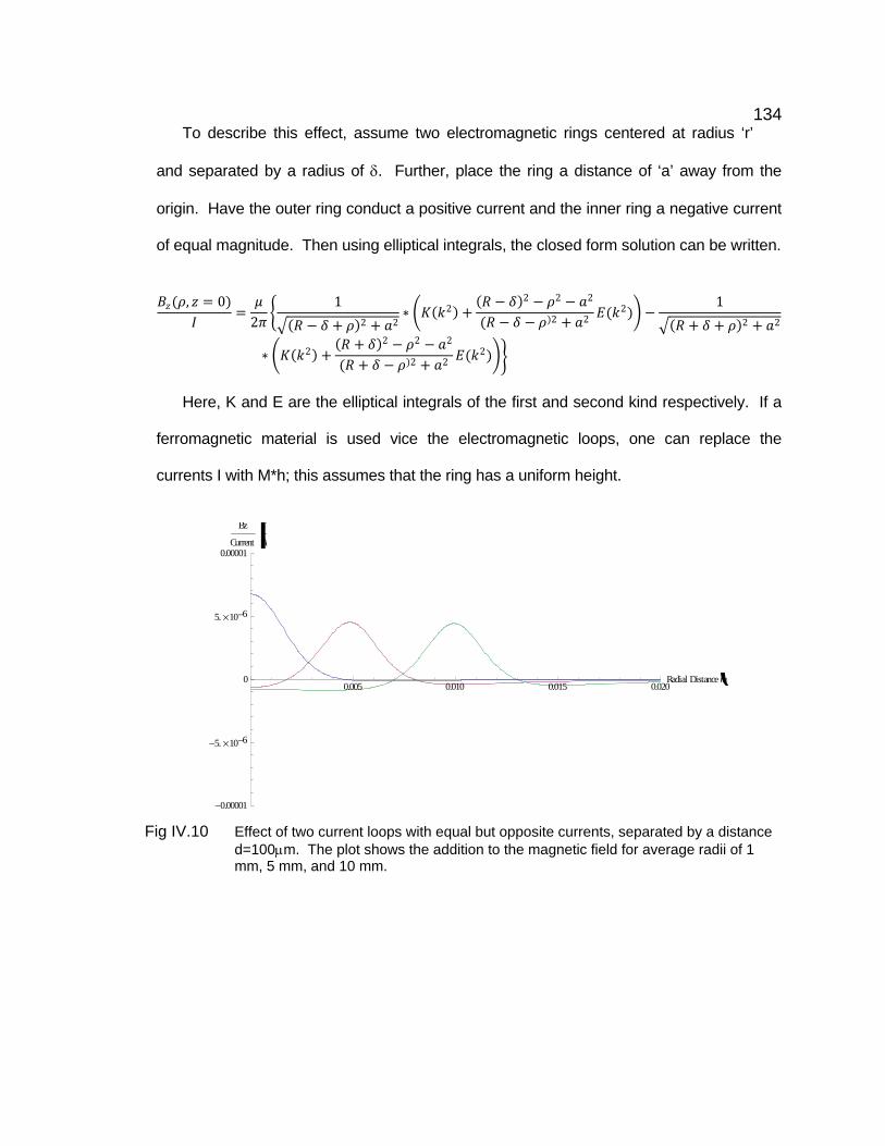
134 To describe this effect, assume two electromagnetic rings centered at radius ‘r’
and separated by a radius of δ. Further, place the ring a distance of ‘a’ away from the
origin. Have the outer ring conduct a positive current and the inner ring a negative current
of equal magnitude. Then using elliptical integrals, the closed form solution can be written.
𝐵𝐵𝑧𝑧(𝜌𝜌, 𝑧𝑧 = 0)𝐼𝐼
=𝜇𝜇
2𝜋𝜋
1(𝑅𝑅 − 𝛿𝛿 + 𝜌𝜌)2 + 𝑎𝑎2
∗ 𝐾𝐾(𝑘𝑘2) +(𝑅𝑅 − 𝛿𝛿)2 − 𝜌𝜌2 − 𝑎𝑎2
(𝑅𝑅 − 𝛿𝛿 − 𝜌𝜌)2 + 𝑎𝑎2 𝐸𝐸(𝑘𝑘2) −1
(𝑅𝑅 + 𝛿𝛿 + 𝜌𝜌)2 + 𝑎𝑎2
∗ 𝐾𝐾(𝑘𝑘2) +(𝑅𝑅 + 𝛿𝛿)2 − 𝜌𝜌2 − 𝑎𝑎2
(𝑅𝑅 + 𝛿𝛿 − 𝜌𝜌)2 + 𝑎𝑎2 𝐸𝐸(𝑘𝑘2)
Here, K and E are the elliptical integrals of the first and second kind respectively. If a
ferromagnetic material is used vice the electromagnetic loops, one can replace the
currents I with M*h; this assumes that the ring has a uniform height.
Fig IV.10 Effect of two current loops with equal but opposite currents, separated by a distance
d=100µm. The plot shows the addition to the magnetic field for average radii of 1 mm, 5 mm, and 10 mm.
0.005 0.010 0.015 0.020Radial Distancem
0.00001
5.106
0
5.106
0.00001
Bz
CurrentTA

135
Fig IV.11 Effect of two current loops with equal but opposite currents, separated by a distance
d=100µm. The plot shows the addition to the magnetic field for average radii of 1 mm, 5 mm, and 10 mm.
A second method to increase the effect of the shim would be to increase the
susceptibility of the ferromagnetic material or increase the thickness. The magnitude of
the effect is useful because with 1 amp, the inhomogeneity can be shimmed past that
achievable from the first magnetic lens. Using these design rules, and the assumption of a
first magnetic lens with a thickness of 20 microns, diameter of 1 inch, and susceptibility of
5000, a set of 5 rings were designed to improve the field homogeneity. The rings were
assumed to have a thickness of 10 microns and susceptibility of 5000. The average radii
and widths of the rings are as follows: 1. 2.025 mm, 50 µm, 2. 3.05mm, 100 µm, 3. 3.55
mm, 100µm, 4. 4.35 mm, 150 µm, and 5. 5.25 mm, 500 µm. These rings were designed
using the finite element simulator previously described. With the design parameters
stated, the magnetic field could be shimmed to less than 50 ppm. This value is
approximately that of the Earth’s magnetic field which would limit the ultimate resolution if
not shielded.
0.002 0.004 0.006 0.008 0.010 0.012 0.014Radial Distancem
0.00001
0
0.00001
0.00002
0.00003
0.00004
Bz
CurrentT
A

136
Fig IV.12 Effect of combination of 5 shims. The locations and widths were designed to counter
the magnetic field inhomogeneity.
Fig IV.13 Effect of adding the shim rings to the collimating lens. The combined effect is a 6
mm diameter range with homogeneity of 50 ppm. These curves were generated using a finite element magnetics simulator.
With the design of both the collimator lens and shim rings complete, fabrication
problems would need to be solved for both structures. Since the shim rings require
precision structures and placement on the micron scale, silicon fabrication was
implemented instead of traditional machining. One of the greatest advantages of the
cryogenic silicon etch is the high selectivity of the etch rate of photoresist over that of
silicon. This advantage can be utilized for improving metallization lift-off on silicon.
0.000 0.002 0.004 0.006 0.008Radial Dista0
5.106
0.00001
0.000015
0.00002
0.000025
Bz
CurrentT
A

137 Typically when lifting off a metallization layer using photoresist, care must be taken in
obtaining resist sidewalls that are vertical or even slightly reentrant, and the photoresist
has to be substantially thicker than the deposited metal layer. The fabrication approach
described here transfers the difficult liftoff profile requirements from the photoresist to the
cryogenic silicon etch. As we demonstrated with the silicon pillars, the sidewall profile is
very easy to control and reproducible by optimizing the cryogenic etch parameters. The
high selectivity improves the relative height between the top of the photoresist to the
silicon surface being metalized thereby permitting thicker metal layers to be deposited.
This enables creation of passive magnetic shims and electromagnetic coils by deposition
of thick layers of iron into silicon. To the authors knowledge, this is the first time using the
etch mask as also the metallization lift-off mask for deposition of thick metal layers on
silicon.
To fabricate the iron rings, two inch p-type silicon wafer were cryogenically etched
simultaneously to approximately 20 microns in depth to define the ring patterns with the
various radii and width describe earlier. Etch conditions were identical to those describe
previously and in Appendix A. With over 1 micron of photoresist remaining, iron was then
thermally evaporated at a rate of 8 A/sec to a final thickness of approximately 6.5 microns.
To reduce stresses from magnetic anisotropy, a 1 inch NdFeB N42 magnet was placed
behind the wafer during evaporation [55]. Following metallization, liftoff was then
performed in acetone. Thicker depositions typically failed due to the film stresses in the
iron layer. It was typical to see layers peel up under what optically appeared to be tensile
stress; this observation is consistent with the thermal coefficients of expansion for iron as
compared to silicon.
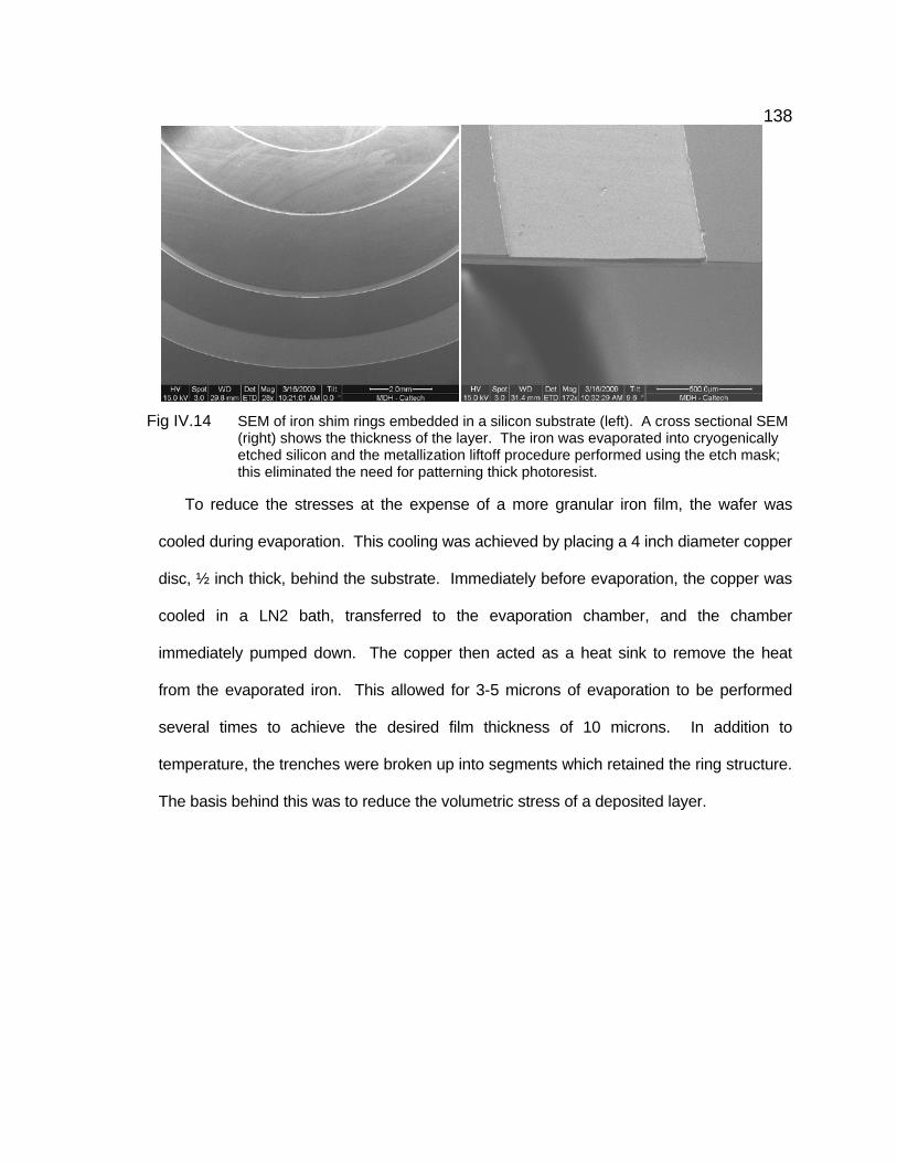
138
Fig IV.14 SEM of iron shim rings embedded in a silicon substrate (left). A cross sectional SEM
(right) shows the thickness of the layer. The iron was evaporated into cryogenically etched silicon and the metallization liftoff procedure performed using the etch mask; this eliminated the need for patterning thick photoresist.
To reduce the stresses at the expense of a more granular iron film, the wafer was
cooled during evaporation. This cooling was achieved by placing a 4 inch diameter copper
disc, ½ inch thick, behind the substrate. Immediately before evaporation, the copper was
cooled in a LN2 bath, transferred to the evaporation chamber, and the chamber
immediately pumped down. The copper then acted as a heat sink to remove the heat
from the evaporated iron. This allowed for 3-5 microns of evaporation to be performed
several times to achieve the desired film thickness of 10 microns. In addition to
temperature, the trenches were broken up into segments which retained the ring structure.
The basis behind this was to reduce the volumetric stress of a deposited layer.

139
Fig IV.15 SEM of iron shim rings embedded in a silicon substrate. By cryogenically cooling the
substrate during evaporation, more than 10 microns of iron were deposited into the etched silicon.
Before the ring structure could be magnetically tested, a collimating lens was required
to improve the homogeneity to closer to a 1000 ppm. Since the metallization layer to
achieve 10 microns already proved a challenge from stresses, deposition of a 1 inch
diameter 20 micron thick iron layer was not attempted. As an alternate route, highly
ferromagnetic metallic glass was used from the Metglas Corporation. Metallic glass is a
metal alloy in which its amorphous state is locked in during cooling; essentially there is no
long range crystalline order. Typically this is done by rapid cooling of the metal from a
liquid state. Metglas 2605s3a was selected for several of its properties. The quoted as
cast susceptibility was > 20,000, the thickness was 0.7 mils (17.8 microns), and the
saturation induction was 1.4 T. The technical specifications of this material can be found
at http://www.metglas.com/downloads/2605s3a.pdf.

140 Initial testing at the time of this writing has shown mixed results. Although the
Metglas proved to be highly ferromagnetic from observation in the magnetic field,
measurements using the Hall Probe indicated otherwise. When the Metglas was placed in
the field, a very strong attraction was noted between the magnet and the shim. Moreover
centering the shim resulted in curling of the edges of the shim to normal with respect to the
magnet. This indicates that the shim is forcing the field to push field lines closer together.
It could be interpreted that this implies a more homogeneous state. This most certainly is
not a conclusive observation since the curling of the shim should also indicate that the field
is reducing the reluctance across the gap by having a ferromagnetic material traversing it.
Magnetic field measurements indicated that the Metglas did have some effect. One layer,
although theoretically should have flattened the field, actually made the field less
homogeneous. But two layers appeared to make the field more homogeneous.
Measurements over many shims under different mounting conditions had the same
enigmatic results. Some configurations resulted in field flattening and some improved the
field.
Fig IV.16 Magnetic field measurements using a Hall Probe mounted on a micrometer stage.
Three conditions were tested, an unshimmed field (black), using one 1 inch diameter

141 Metglas 2605s3a shim (blue), and using two 1 inch diameter Metglas 2605s3a shims (red).
It is quite likely that difficulty in measuring the homogeneity could be due to the
measurement device itself or part of the holder design [56]. Although the probe is rated to
measure 1 Gauss in a 3 Tesla field, it is not clear whether having the probe in the field
actually perturbs the field homogeneity. It is known that when shimming NMR machines
most operators use the measurement of the NMR spectra as the determining factor for the
true field homogeneity. Unfortunately, it is impossible to test the second lens before the
first lens is in place. The main reason is that the purpose of the second lens was to take a
known field and shim it to homogeneity. Placing the second lens in the magnetic field and
expecting it to operate correctly is akin to using a telescope objective without the main
telescope mirror. It is possible the field is homogeneous enough over a large enough
sample volume that it would be possible to measure spectra and use this to determine the
effects of shim additions. Indeed, it was noted that over a 1.5 mm, a sub 100 ppm field
homogeneity exists. Setting up a method to accurately measure the magnetic field to high
homogeneity is the next logical step for this project.
Copper Planar Microcoils
As a second major component of the portable NMR system, transmission and
detection coils were fabricated on silicon [57]. By creating the microcoils in silicon vice
winding copper coils from wire, the fabrication process can reduce the cost and increase
the repeatability of the microcoil [58,59,60,61,62,63]. This microcoil is designed to also act
as a resonator whose resonance is placed according to the gyromagnetic ratio of the
nuclei being detected. This section will detail the design of the microcoils both as an

142 electrical component in a circuit as well as the electromagnetic field generation. A
fabrication sequence will detail how to create these microcoils in silicon using a single
lithographic step. Finally, the electrical characteristics, both DC and AC, as well as the
electromagnetic field are measured and described for the coils. It should be emphasized
that this planar microcoil is designed for NMR applications but should not be limited to
such. For example, this design is CMOS compatible so an ideal use might be increasing
the inductance for use in an integrated switcher or for a microfluidic susceptibility detector
[64].
The basis of the microcoil design was to optimize their signal to noise ratio (SNR) for
use in NMR experiments [53,61,65]. In NMR experiments, changing the nuclei that are
observed or changing the strength of the polarizing magnetic field also changes the
Larmor frequency at which the signal is observed. Further, the signal to noise ratio of the
experiment is proportional to the field produced by the coil, the noise generated by the
Johnson resistance of the coil, and the number of nuclei being observed or volume of the
sample. Hence, the design of the geometry of a NMR coil is initially based on maximizing
the SNR for a chosen frequency, which then determined the required inductance and
resistance of the coil.
𝑆𝑆𝑁𝑁𝑅𝑅 = 𝛾𝛾3ℏ2 ∗ 𝐵𝐵2 ∗ 𝛽𝛽 ∗ 𝐼𝐼(𝐼𝐼 + 1) ∗ 𝑁𝑁𝑠𝑠𝑎𝑎𝜇𝜇𝑠𝑠𝑠𝑠𝑚𝑚
3 ∗ 4 ∗ 𝑅𝑅𝑚𝑚𝑠𝑠𝑐𝑐𝑠𝑠𝑑𝑑𝑎𝑎𝐿𝐿𝑐𝑐𝑚𝑚 ∗ ∆𝑓𝑓𝛽𝛽
∗ 𝐵𝐵1
𝑐𝑐𝑠𝑠𝑐𝑐𝑐𝑐𝑚𝑚𝐿𝐿𝑑𝑑d𝒱𝒱
Here γ is the gyromagnetic ratio (γ=42.58 MHz/T for protons), h-bar is Planck’s
constant, B is the polarizing magnetic field created by the permanent magnet setup, I is
the spin (1/2 for proton), Nsample is the number of spins generating a signal per unit volume,
Resistance is the total resistance of the coil, β is Boltzmann’s constant times the

143 temperature, ∆f is the bandwidth of the circuit used, and the integral describes the
magnetic field generated by the planar microcoil (B1) over the sample volume per Amp.
To achieve the highest SNR, geometrically, the optimization of the microcoil involves
the resistance, and the integrated terms. To some extent the bandwidth is also modified,
but an external matching circuit was utilized to further reduce the bandwidth. To
numerically model the microcoils, the classic NMR SNR equation is recast into a more
transparent form.
𝑆𝑆𝑁𝑁𝑅𝑅 = ω ∗ Mo
4 ∗ 𝑅𝑅𝑚𝑚𝑠𝑠𝑐𝑐𝑠𝑠𝑑𝑑𝑎𝑎𝐿𝐿𝑐𝑐𝑚𝑚 ∗ ∆𝑓𝑓𝛽𝛽
∗ 𝐵𝐵1
𝑐𝑐𝑠𝑠𝑐𝑐𝑐𝑐𝑚𝑚𝐿𝐿𝑑𝑑d𝒱𝒱
Mo = Nsγ2ℏ2I(I + 1)Bo
3KBT~0.0032021 𝑑𝑑𝜇𝜇𝑠𝑠 𝜇𝜇−1
To accurately model the electromagnetic field of the coil, FEMM was employed to
simulate the microcoil around the frequency of interest. The simulations were performed
for an increasing number of coil turns to determine the optimal number. This simulation
permits coupling of the coil’s turns and accounts for skin depth in the copper conductor
(approximately 9.5 microns at 50 MHz) and assumed a 1.15 T polarizing field (ω=γ*Bo~50
MHz). Four starting radii were selected to test the silicon based microcoil detection; 980
micron, 730 micron, 480 micron and 230 micron radii. All of the coils had wire widths of 40
microns at 70 micron center-to-center spacing based on what was achievable from the
fabrication process. The sample volume of all the simulations incorporated a volume of
diameter equal to that of the first turn of the microcoil and a height determined by a radius
to height ratio of 0.08. From the simulations, several parameters were retrieved, most
importantly the integral over the volume, the resistance at high frequency, the magnetic

144 field the microcoil can generate from 1 Amp of current, and approximation of the signal
size to be detected.
Fig IV.17 Simulation of Bz field for a 500 micron radius planar microcoil. The simulation was
run at 50 MHz for a 2 turn microcoil. These FEMM simulations allowed for the signal to noise ratio to be optimized.
Fig IV.18 Simulation of the signal to noise ratio for the various microcoils. These FEMM
simulations allowed for the signal to noise ratio to be optimized.

145 Using the simulations it was determined that for the 1000, 750, and 500 micron
radius coils, 2 turns would be used and only 1 turn for the 250 micron radius coil. As a
verification of the simulations, an analytical solution was numerically calculated in
Mathematica for the 2 turn coils. To calculate the magnetic field, the full solution to a
planar coil was used [66].
𝐵𝐵𝑧𝑧(𝜌𝜌, 𝑧𝑧) = 𝜇𝜇 ∗𝜌𝜌
((𝑅𝑅 + 𝛿𝛿𝐿𝐿)2 + 𝑧𝑧2∗ (𝐸𝐸𝑠𝑠𝑠𝑠𝑐𝑐𝑠𝑠𝑑𝑑𝑐𝑐𝑐𝑐𝐾𝐾
4 ∗ (𝑅𝑅 + 𝛿𝛿𝐿𝐿) ∗ 𝜌𝜌((𝑅𝑅 + 𝛿𝛿𝐿𝐿)2 + 𝑧𝑧2
+((𝑅𝑅 + 𝛿𝛿𝐿𝐿 − 𝜌𝜌)2 − 𝑧𝑧2)((𝑅𝑅 + 𝛿𝛿𝐿𝐿 − 𝜌𝜌)2 + 𝑧𝑧2)
1
𝐿𝐿=0
∗ 𝐸𝐸𝑠𝑠𝑠𝑠𝑐𝑐𝑠𝑠𝑑𝑑𝑐𝑐𝑐𝑐𝐸𝐸 4 ∗ (𝑅𝑅 + 𝛿𝛿𝐿𝐿) ∗ 𝜌𝜌((𝑅𝑅 + 𝛿𝛿𝐿𝐿)2 + 𝑧𝑧2
)
The summation was used to account for each of the coil’s turns but did not include the
inductive coupling from one turn to another. A similar summation was used to calculate
resistance with the width of the wire limited to 2 times the skin depth for copper (9.4
microns). A final assumption was that the substrate has no conductivity which would
otherwise degrade the inductance. Although these three assumptions assist in making the
calculations tractable, they do not accurately model the coils. In fact the skin depth adds
considerably more resistance at 50 MHz than modeled and reduction of the inductance
due to coupling and the substrate will be seen to dramatically decrease the ‘Q’ of the
inductor [67]. However, the calculation does serve as a validity check for the simulations.
The results from the calculations, found in the Appendix, are seen in the following table:
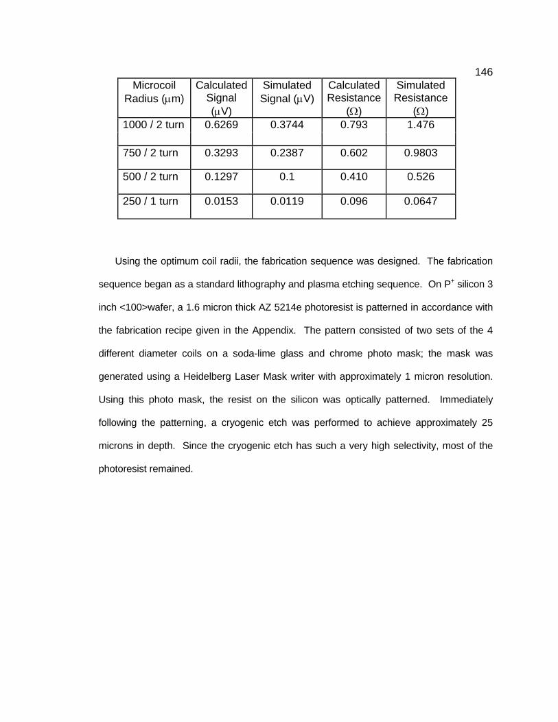
146 Microcoil
Radius (µm) Calculated
Signal (µV)
Simulated Signal (µV)
Calculated Resistance
(Ω)
Simulated Resistance
(Ω) 1000 / 2 turn 0.6269 0.3744 0.793 1.476
750 / 2 turn 0.3293 0.2387 0.602 0.9803
500 / 2 turn 0.1297 0.1 0.410 0.526
250 / 1 turn 0.0153 0.0119 0.096 0.0647
Using the optimum coil radii, the fabrication sequence was designed. The fabrication
sequence began as a standard lithography and plasma etching sequence. On P+ silicon 3
inch <100>wafer, a 1.6 micron thick AZ 5214e photoresist is patterned in accordance with
the fabrication recipe given in the Appendix. The pattern consisted of two sets of the 4
different diameter coils on a soda-lime glass and chrome photo mask; the mask was
generated using a Heidelberg Laser Mask writer with approximately 1 micron resolution.
Using this photo mask, the resist on the silicon was optically patterned. Immediately
following the patterning, a cryogenic etch was performed to achieve approximately 25
microns in depth. Since the cryogenic etch has such a very high selectivity, most of the
photoresist remained.

147
Fig IV.19 Cross sectional SEM of a microcoil ridge separating two trenches where copper was
to be deposited. The cryogenic silicon etch was masked with 1.6 microns of resist. Following the etch, an insulating 1.6 micron thick silicon dioxide layer was PECVD deposited.
At this point, one of two techniques of low temperature chemical vapor deposition
(CVD) were used to deposit an insulating layer of silicon dioxide. This insulating layer
prevented the current from leaving the copper wire runs and going to the substrate. This
layer also created a parasitic capacitance which will be discussed later. The first
technique utilized an ICPRIE fitted with a gas ring around the table. This unique gas ring
configuration permits the injection of 5% Silane diluted with nitrogen, 5%-SiH4/N2, into the
chamber for creation of a plasma. When nitrous oxide, N2O, is injected into the plasma
the result is a recombination of the silicon atom and the oxygen atom to create a silicon
dioxide deposition. This technique is referred to as ICP-CVD. This method of deposition is
advantageous since no Fwd power is required and the table temperature is approximately
90 C. The low temperature prevents the resist from cross-linking or burning. A very
dense layer of silicon dioxide deposits at a rate of approximately 18 nm per minute and

148 typical deposition times were 2 to 8 minutes; 8 minutes results in approximately 140
nm. To improve the adhesion of metal to the silicon dioxide layer, a 2 min deposition of
amorphous silicon was deposited; the recipe is the same as the silicon dioxide but the
nitrous oxide flow was stopped.
SiH4/N2 100 sccm ICP Power 2000 W
N2O 15 sccm Fwd Power 0
Temperature 90 C Pressure 5 mT
A second technique for silicon dioxide deposition was using plasma enhanced
chemical vapor deposition (PECVD). This instrument was also an Oxford Instruments
Plasmalab System 100 but is physically different from an ICPRIE in that it does not have
an ICP coil. Instead, the machine uses a CCP with both a 13.56 MHz RF power supply
and a low frequency power supply. The low frequency supply has an output low pass filter
which limits the output frequency to less than 100 KHz. The addition of the lower
frequency power supply permits stress built up during the deposition to be controlled.
Since the plasma is not as dense as the ICPRIE, the table temperature is required to be
much hotter to achieve a similar density in the layers when compared to the ICP-CVD;
standard temperatures are 350 C to 400 C. Since photoresist was used in this process,
the temperature was limited to less than 150 C, reducing the quality of the layer. Typical
deposition rates using this machine were 65 nm per minute and were typically run for 20
seconds. Again to achieve better adhesion between the metal and oxide, by stopping the
nitrous oxide gas flow a thin layer of amorphous silicon was deposited.

149 SiH4/N2 450 sccm HF Power 15 W
N2O 750 sccm Fwd Power 0
Temperature <150 C Pressure 1 T
SiH4/N2 280 sccm HF Power 50 W
Fwd Power 0
Temperature <150 C Pressure 2 T
Fig IV.20 Deposition rate of low temperature PECVD of Silicon Dioxide. Data was fitted to a
linear deposition rate of 42 nm per minute with an offset of 207 nm. This data is untested for less than 20 minute deposition times.
Upon completion of the silicon dioxide insulating layer, one final step was needed
before deposition of the copper. This step was exposing clean silicon substrate at the end
of the innermost wire run. Having clean, highly doped P-type silicon and copper come into
contact, an Ohmic tunnel-junction could be made. An Ohmic contact is made by one of 2
methods: matching the metal and semiconductor work functions to lower the barrier height
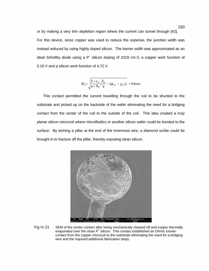
150 or by making a very thin depletion region where the current can tunnel through [42].
For this device, since copper was used to reduce the expense, the junction width was
instead reduced by using highly doped silicon. The barrier width was approximated as an
ideal Schottky diode using a P+ silicon doping of 1019 cm-3, a copper work function of
5.10 V and a silicon work function of 4.72 V.
𝑑𝑑𝑃𝑃~2 ∗ 𝜖𝜖𝑠𝑠𝑐𝑐𝑞𝑞 ∗ 𝑁𝑁𝑑𝑑
(𝐸𝐸𝑔𝑔𝑞𝑞− (𝜙𝜙𝑐𝑐𝑠𝑠 − 𝜒𝜒𝑠𝑠𝑐𝑐)) ~9.8𝐿𝐿𝜇𝜇
This contact permitted the current travelling through the coil to be shunted to the
substrate and picked up on the backside of the wafer eliminating the need for a bridging
contact from the center of the coil to the outside of the coil. This idea created a truly
planar silicon microcoil where microfluidics or another silicon wafer could be bonded to the
surface. By etching a pillar at the end of the innermost wire, a diamond scribe could be
brought in to fracture off the pillar, thereby exposing clean silicon.
Fig IV.21 SEM of the center contact after being mechanically cleaved off and copper thermally
evaporated over the clean P+ silicon. This contact established an Ohmic tunnel-contact from the copper microcoil to the substrate eliminating the need for a bridging wire and the required additional fabrication steps.

151 Immediately following the removal of the contact pillar, a thermal evaporation of
copper was performed. The thermal evaporator used was pumped down to approximately
5x10⁻⁶ Torr. The boats used were R.D. Mathis RDM-WBAO-3 alumina coated tungsten
boats allowing for approximately fifteen 50 g copper slugs to be evaporated at the same
time. This permitted approximately 5 microns per run to be deposited. Evaporation rates
were approximately 20 – 40 Angstroms per second with a plate temperature set at 41 C.
Upon completion of the evaporation, the sample was allowed to cool for two hours before
vacuum was broken. To perform liftoff, the sample was immersed in acetone where the
metal on top of the resist would peel off, usually in one single foil sheet leaving the copper
in the etched trenches. To create the backside contact, the wafer was floated in BHF
(floating denotes that the wafer was placed on top of the HF solution and would float on
the top of the fluid so only the back side of the wafer made contact with the solution). The
backside silicon was cleaned for 1 minute, rinsed with DI, dried with N2, and placed in the
evaporator where 100-300 nm of copper was then evaporated.
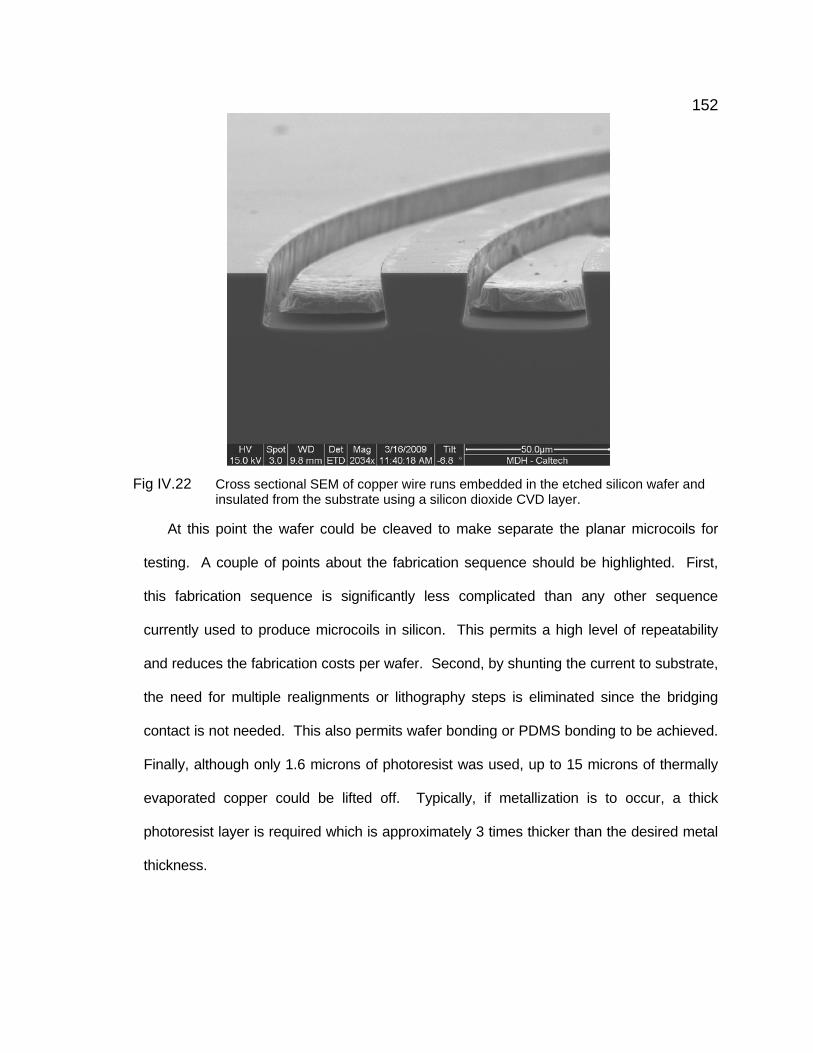
152
Fig IV.22 Cross sectional SEM of copper wire runs embedded in the etched silicon wafer and
insulated from the substrate using a silicon dioxide CVD layer.
At this point the wafer could be cleaved to make separate the planar microcoils for
testing. A couple of points about the fabrication sequence should be highlighted. First,
this fabrication sequence is significantly less complicated than any other sequence
currently used to produce microcoils in silicon. This permits a high level of repeatability
and reduces the fabrication costs per wafer. Second, by shunting the current to substrate,
the need for multiple realignments or lithography steps is eliminated since the bridging
contact is not needed. This also permits wafer bonding or PDMS bonding to be achieved.
Finally, although only 1.6 microns of photoresist was used, up to 15 microns of thermally
evaporated copper could be lifted off. Typically, if metallization is to occur, a thick
photoresist layer is required which is approximately 3 times thicker than the desired metal
thickness.

153
Fig IV.23 SEM of silicon planar microcoil with radius of 1000 microns. The center contact
shunts the current to substrate via Ohmic contact.
To confirm the fabrication work, the microcoils are first electrically tested under DC
conditions. The first test uses an Agilent Semiconductor Parameter Analyzer 4155 to
sweep biasing voltage negative to positive while measuring the current. Although this is a
two probe measurement and has the problem of introducing series resistance in the
measurement from the leads, it allows for the verification that the copper silicon contacts
are indeed Ohmic vice a Schottky rectifying diode. This measurement does not provide
an accurate measurement of contact or coil resistance. One aspect to note is that a
current compliance was implemented in the measurement, so once this current is met any
increase in voltage will not increase the current further. This is seen in the graphs as a
diagonal line. The spike at zero is due to a numerical divide by zero calculation and a
short circuit measurement of approximately 3.98 Ohms was made. The most important
aspect of this measurement is that the copper-silicon junction is Ohmic to under 0.1 Ohms.

154 Since a 50 MHz AC signal is used for the NMR experiments, any rectification of the
signal will introduce errors in the detection.
Fig IV.24 Resistance of a 2 probe measurement of planar microcoils taken using an Agilent
Semiconductor Parameter Analyzer. Measured lead resistance was 1.9 Ohms (from probe tip to probe tip). The diagonal line is when the machine enters current compliance and will not permit the current to increase. The flat resistance denotes that the copper silicon contact is Ohmic to under 50 mΩ.
To more accurately measure the DC resistance, a 4 point probe measurement was
made using a Keithley 2400 source-meter. This type of measurement, also referred to as
a Kelvin measurement, injects current into the device while using two other probes to
measure the voltage across different components. Since the voltage measurement draws
little to zero current, probing the device yields a more accurate measurement. The
devices tested had an approximately 7 micron thick copper layer, half as thick as the
calculations. The measured results are displayed with simulated results under DC
conditions for a 15 micron thick layer. Comparison between the two resistances shows
very good agreement upon a multiplier of 2 due to the thickness difference.

155
Microcoil Radius (µm) Measured Coil and Lead Resistance (Ω) ~ 7 micron
thick copper
Simulated Coil and Lead Resistance (Ω) – 15 micron thick copper
1000 / 2 turn 0.716 0.375
750 / 2 turn 0.624 0.284
500 / 2 turn 0.326 0.194
To ensure the magnetic field generated was close to simulations, a Hall probe and
LakeShore 455 Gauss meter was used to measure the Bz field at the center of coil along
the axis. Using the Keithley 2400 multimeter to supply 1 amp to the coils, the magnetic
field was measured using the Hall probe on a 3 stage micrometer. First the center of the
coil was determined in the ‘x’ and ‘y’ directions by finding the maxima. The Hall probe was
then moved as close to the substrate as possible, the current turned off and the Gauss
meter zeroed. This measurement was also normal to the Earth’s 50 µT magnetic field
which eliminated this variable from the measurement. The current was then turned back
on, and the probe lifted in 50 micron increments. This measurement permits the
complicated magnetic field measurement to be simplified.
𝐵𝐵𝑧𝑧(𝑧𝑧) =𝐿𝐿𝜇𝜇𝐼𝐼
2∗
𝑅𝑅2
(𝑅𝑅2 + (𝑍𝑍 + 𝑍𝑍𝑐𝑐)2)32
Here, n is the number of turns on the coil, I is the current (1 Amp), µ is the permeability
R is the radius of the coil, and Z and Zo the height above the coil and the offset from zero.
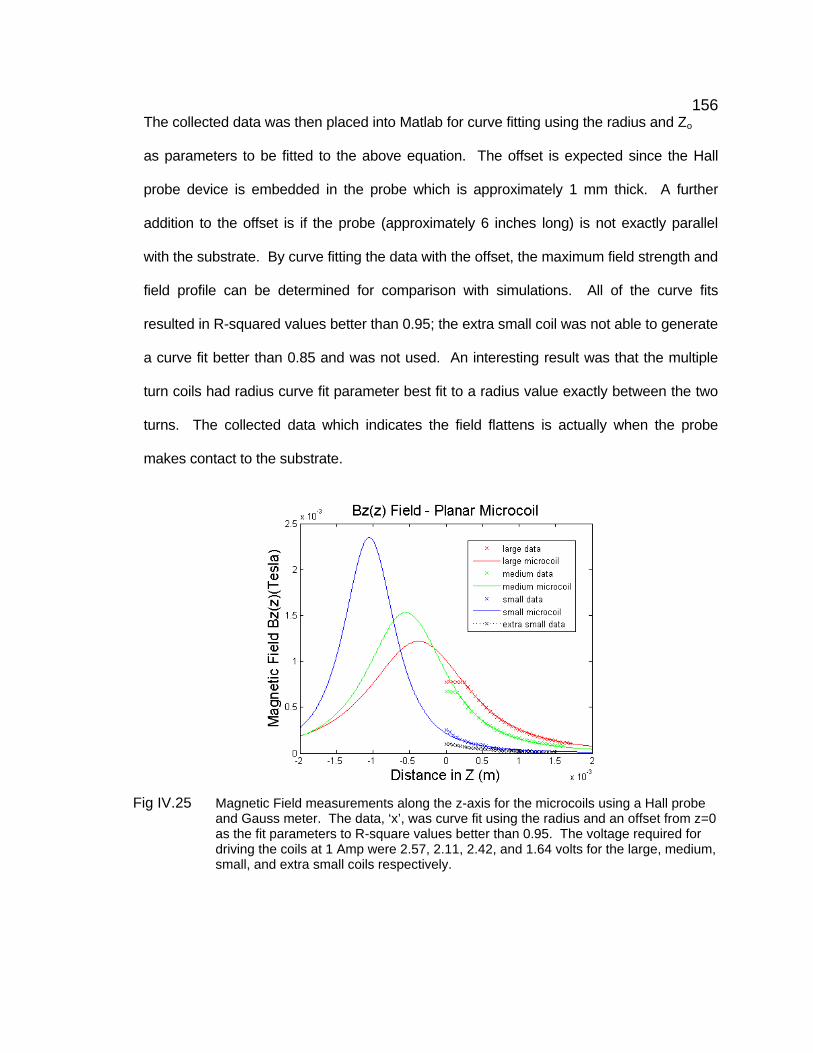
156 The collected data was then placed into Matlab for curve fitting using the radius and Zo
as parameters to be fitted to the above equation. The offset is expected since the Hall
probe device is embedded in the probe which is approximately 1 mm thick. A further
addition to the offset is if the probe (approximately 6 inches long) is not exactly parallel
with the substrate. By curve fitting the data with the offset, the maximum field strength and
field profile can be determined for comparison with simulations. All of the curve fits
resulted in R-squared values better than 0.95; the extra small coil was not able to generate
a curve fit better than 0.85 and was not used. An interesting result was that the multiple
turn coils had radius curve fit parameter best fit to a radius value exactly between the two
turns. The collected data which indicates the field flattens is actually when the probe
makes contact to the substrate.
Fig IV.25 Magnetic Field measurements along the z-axis for the microcoils using a Hall probe
and Gauss meter. The data, ‘x’, was curve fit using the radius and an offset from z=0 as the fit parameters to R-square values better than 0.95. The voltage required for driving the coils at 1 Amp were 2.57, 2.11, 2.42, and 1.64 volts for the large, medium, small, and extra small coils respectively.

157
Fig IV.26 Magnetic Field simulations in FEMM along the z-axis for the microcoils. This
simulation was for a DC current of 1 Amp and shows very good agreement with measurements.
Although the DC measurements assist in confirmation that the planar microcoil
operates as design, the microcoil was intended for use as a 50 MHz NMR detector. For
this purpose, it was seen that the bandwidth of the microcoil needed to be as narrow as
possible to reduce the detected noise. Desiring a narrow bandwidth is synonymously
asking for a high ‘Q’. For this microcoil, the ideal ‘Q’ is the same for an ideal inductor.
𝑄𝑄 =𝜔𝜔Δ𝜔𝜔
=𝜔𝜔𝐿𝐿𝑅𝑅
These ‘Q’ values are significantly lower than handwound coils where more typical ‘Q’s
are in the range of 30. The values are also much lower than current published work on
Microcoil Radius (µm)
Simulated Resistance at 50 MHz (Ω)
Simulated Inductance at 50 MHz (H)
Simulated 'Q' at 50 MHz
1000 / 2 turn 1.476 15.84 *10-9 3.4750 / 2 turn 0.9803 11.74 *10-9 3.8500 / 2 turn 0.5258 7.50 *10-9 4.5

158 planar microcoils for NMR. Massin et al. demonstrated ‘Q’s of 17-19 for similar
shaped microcoils fabricated on glass slides but operated at 300 MHz (approximately 6
times the frequency). It should be noted that their fabrication sequence required the use
of a bridging contact. Taking the frequency into account, these coils should have a
comparable ‘Q’. It was hypothesized the low ‘Q’s in designed microcoils might be due to
the highly resistive silicon substrate used. To test this, simulations were performed at 46
MHz using the 1000 micron radius coil, the large coil. The substrate resistivity was then
adjusted to the following values and simulated: 5 mΩ-cm, 10 Ω-cm, and 1000 Ω-cm. The
simulated ‘Q’s were noted to increase rapidly from 3.46, 11.58, and 11.60 respectively.
Unfortunately, the Ohmic center contact relied on the highly doped silicon; 10 Ω-cm has an
approximate doping of 1015 for a depletion width of 980 nm, and 1000 Ω-cm has an
approximate doping of 1013 for a depletion width of 9.8 microns. These barrier widths
would not permit the bridgeless Ohmic tunnel contact. The ‘engineering trade-off’ made
then is the fabrication simplicity for a reduced ‘Q’. One might argue that the copper runs
should be made thicker in order to reduce the resistance. Unfortunately, the skin depth of
9.4 microns makes this task have diminishing returns after about 10 microns. One
potential direction is to use a thick epitaxial P+ deposited on a 10 Ω-cm substrate; when
the Ohmic contact is made it would be using P+ silicon but the losses due to the substrate
can be dramatically reduced.
To externally meet the demands of using a narrow bandwidth, a discrete component
circuit was designed, simulated, and tested. This discrete circuit is very similar to the
matching circuit used to tune ICP coils described in Chapter 1 and that analysis will be
referred to here. Since each coil run is insulated from the substrate by a thin oxide layer,
this parasitic capacitance needs to be accounted for. To do this the areal foot print is

159 broken into two parts, the area under the coil and the area under the contact pad. The
thickness of the oxide layer defines the dielectric thickness; since thermal evaporation has
very poor step coverage, it is assumed that the sidewalls contribute negligible
capacitance. Then using the simulated inductance and resistance, the parasitic devices
can be accounted for. An approximation of 0.5 Ω for the Ohmic contact resistance is
used.
Microcoil Radius
(microns) Coil Area (10-9 m2)
Coil Capacitance 140 nm oxide
Pad Area (10-6 m2)
Pad Capacitance 140 nm oxide
Simulated Inductance
(nH)
Simulated Resistance
(Ω) 1000 / 2 turns 520.25 1.28318E-10 1.372 3.384E-10 15.84 1.48 750 / 2 turns 394.58 9.7322E-11 2.441 6.02066E-10 11.74 0.98 500 / 2 turns 268.92 6.63283E-11 4.617 1.13877E-09 7.5 0.53
Careful account of the amount of capacitance the pad area and the oxide thickness
contributes permits the planar microcoils to attain a ‘natural’ resonant frequency. Hence
the silicon planar microcoils are designed to have an integrated resonant frequency. The
naïve calculation using only the capacitance and inductance yields the following
frequencies.
Microcoil Radius
(microns)
Coil Resonance
(MHz) 1000 / 2 turns 58.54 750 / 2 turns 55.54 500 / 2 turns 52.94
Although having the circuit tuned automatically based on geometrical and fabrication
controls is useful for a theoretical circuit, inevitably experimental variations in a microfab
setting introduce variations to device parameters. Experimental engineers are commonly

160 heard cynically stating, “the simulations are amazing.” To account for the
experimental variations, two trimmer capacitors are utilized in configurations similar to that
of the ICP power matching circuit [57]. This circuit was simulated using Top Spice (a
graphical circuit simulator) using the solved for C1 and C2 nominal values. It was found
that approximately 150 pF was needed to tune the coil down to 50 MHz region (the parallel
capacitor) and several nano Farads were need to match the phase (the series capacitor).
This circuit was implemented on a PCB board with surface mounted capacitors. The
silicon microcoil was placed flat on the board with the backside making contact to copper
PCB runs. The silicon was held in place using a modified copper alligator clip; this clip
was trimmed to the width of the contact pad and was used to make electrical contact to the
planar microcoil. Two non-ferromagnetic tunable capacitors which ranged in value from 0-
120 pF were used in parallel with a 85 pF Tantalum capacitors to act as the tunable
parallel capacitor. For the series capacitor, two of the 0-120 capacitors were used.
Fig IV.27 Top Spice schematic of the large planar microcoil. This model includes the parasitic
capacitances of the coil and contact pad, the coil, lead wires, and Ohmic contact resistances, and adds matching capacitors C1 and C2 (used to tune the circuits resonance).

161
Fig IV.28 Top Spice simulation of the large planar microcoil. This model includes the parasitic
capacitances of the coil and contact pad, the coil, lead wires, and Ohmic contact resistances, and adds matching capacitors C1 and C2 (used to tune the circuits resonance).
The frequency measurements were performed on an Agilent 8712 ET Network
Analyzer with frequency sweeps generally from 0.3 to 100 MHz; refined sweeps were
used for more accurate measurements. With a 50 ohm coax cable, the machine was
normalized (effectively zeroing out the reading) after a self calibration. Whenever the
frequency range or type of measurement was changed, this normalization procedure was
performed. As an external check, a 50 ohm termination plug was used to verify accuracy.
The first measurement was to measure the ‘Q’ of the circuit holder; at 50 MHz and tuned
with the capacitors the ‘Q’ was approximately 262.
M[
02
4
6
8
10
12
14
16
18
20
22
24
26
2830
M[=V(VIN
)/I(RSO
UR
CE)]
0 20 40 60 80 100
FREQUENCY (MHz)
P[
-100
-75
-50
-25
0
25
P[=V(VIN)/I(R
SOU
RC
E)] (W)
0 20 40 60 80 100
FREQUENCY (MHz)

162
Fig IV.29 Reflectance measurement using a Network Analyzer of the microcoil chip holder.
The measured ‘Q’ is approximately 262, with the y-axis in dB.
Fig IV.30 Reflectance measurement using a Network Analyzer of the silicon planar microcoils.
The measured ‘Q’s are approximately 22, 5.9, 7.0, and 6.3 for the extra small, small, medium, and large coils.
Next the microcoils were measured using same technique. For this particular set of
microcoils, 20 mΩ-cm resistivity P+ silicon was used. As noted earlier, less conductive
silicon resulted in higher ‘Q’ values. A typical measurement of microcoils fabricated on 5

163 mΩ-cm resistivity P+ silicon yielded ‘Q’ values of 7.4, 3, 1.5, and 1.3 for the extra
small, small, medium and large microcoils respectively. The increase in resistivity yielded
significantly better ‘Q’s, 22, 5.9, 7.0, and 6.3 respectively.
With the coils tuned to the correct frequency, the next test is to place the coils in the
magnetic field and run NMR pulse sequences and analyze the detected signal. By
measuring the decay rate of a known signal, say water, the decoherence rate can be
measured. This decoherence can be shown to be a combination of the natural decay rate
plus the inhomogeneity of the magnetic field. For an apparatus such as the one built here,
a good approximation is that the inhomogeneity of the field dominates.
1𝑇𝑇2∗ = 1
𝑇𝑇2 + 𝛾𝛾 ∙ ∆𝐵𝐵𝑐𝑐
Here T2* describes the total decoherence time, T2 describes the natural decoherence
time, γ is the gyromagnetic ratio, and ∆Bo is the magnetic field inhomogeneity. For the
unshimmed magnetic field described earlier and assuming a natural decoherence time of
a few hundred milli-seconds, the field would need to be shimmed to better than 1 ppm to
see the natural decoherence times. For this reason, it is typical to measure the shimming
of the magnetic fields using these coils while simultaneously backing out information on
the exact SNR. Further description of the microcoils will need to wait until the magnetic
field can be shimmed to a useful homogeneity.
Silicon Micropillars Point Schottky Diodes To understand the contact made between the silicon nanowires and the tungsten
probe tip, micropillars were utilized for their much lower surface to volume ratio. These
devices were fabricated using identical silicon and cleaning methods as those used for the
nanowires and tested in a manner identical. The information gathered demonstrated

164 several experimental aspects which were hypnotized but untested for the nanowires.
One of the differences seen between the micropillars and the nanowires was due to the
size of the probe tip in relation to the wire itself. This section will detail the work
performed, methods used, and results.
This fabrication sequence was a combination of the nanowire and cryogenic etching.
Using 2” P+ silicon wafers, crystal orientation of <100>, photoresist was placed on the
wafer and patterned using the hexagonal hole pattern described in chapter 1. Using resist
reversal 50, 20, 10, and 5 micron diameter discs were patterned on the silicon in
hexagonal arrays separated by lengths equal to their diameters. A silicon cryogenic etch
was then performed for 25 minutes under the following conditions:
SF6 70 sccm ICP Power 900 W
O2 6.5 sccm Fwd Power 8 W
Temperature -130 C Pressure 10 mt
The pillar arrays were then measured in a Nova 600 dual beam SEM for the diameters
and heights: 50.90/26.87, 21.14/25.46, 11.75/25.19, and 5.81/23.25 microns. The
variation in etch height, although etched at the same time, is due to aspect ratio
dependent etching discussed and described in Chapter 1. The resist was then removed
using acetone. A silicon cleaning, identical to that performed for the nanowires, was then
performed. This consisted of three cycles of: RCA 1 cleaning (3:1.5 of NH4OH:H2O2 at
90C) for 3 minutes, DI rinse, 1 minute of BHF clean, followed by DI rinse. Immediately
before testing, the sample was BHF dipped for 1 minute to hydrogen terminate the
dangling silicon bonds on the surface.

165 Upon completion of cleaning, the pillars were mounted on a 90 degree probe
stage in the Quanta SEM using copper adhesion tape. One probe contacted the copper
tape on the back side while one probe tip was carefully brought down to make contact with
the top of the pillar being tested. The probe tips were electrically connected to an Agilent
Semiconductor Parameter Analyzer 4155 C for I-V curve generation. During
measurement, the SEM beam was blanked to prevent electron beam induced charge
carriers from being produced. The internal IR camera was also turned off to prevent
photo-generated carriers from being produced.
Fig IV.31 SEM taken in the Quanta as a 10 micron diameter pillar was contacted with a
tungsten probe tip.
What had been assumed with the nanowires was that the highly doped silicon and
tungsten probe tip would make an Ohmic tunnel contact and that the area of the backside
diode was large enough to make the resistance the diode contributed negligible (in effect,
making the backside contact an Ohmic contact). Qualitatively what was seen

166 fundamentally with a positive voltage on the probe tip and ground on backside, was as
follows: a reverse biased point contact diode from the tungsten probe tip to the top of the
silicon micropillar. The backside contact seemed to be an Ohmic contact as predicted.
The tungsten-silicon diode is described by the classical Schottky diode equation:
𝐽𝐽 = 𝐽𝐽𝑐𝑐 𝑚𝑚𝑉𝑉𝑃𝑃𝜂𝜂𝑉𝑉𝑇𝑇 = 𝑑𝑑∗∗𝑇𝑇2 ∙ 𝑚𝑚−
𝜙𝜙𝐵𝐵𝑠𝑠𝑅𝑅𝑑𝑑 ∙ 𝑚𝑚
𝑉𝑉𝑃𝑃+Δ𝜙𝜙𝑉𝑉𝑇𝑇
In these equations, it is assumed that the voltage across the diode is more than a few
KbT/q so the ‘-1’ term can be ignored. Here η is the ideality factor, Jo is the saturation
current density, φbp is the junction barrier height, ∆φ is the voltage dependant barrier height
lowering and VTt is KbT/q or 0.02582 V. In reverse bias, the leakage current is
approximated to be Jo and any voltage dependence is due to image charge barrier height
lowering. Since the probe contact is small, the current density is determined by
approximating the area of the probe contact as the diode area. This area is the same for
all the pillars. As a test case, the probe was also placed on the substrate and the I-V
curve measured.

167
Fig IV.32 I-V measurements of the silicon micropillars etched 25 microns tall. The pillars were
cleaned, mounted in the SEM, and measured identically to that of the nanopillars. The tungsten probe tip creates a Schottky diode and the backside contact is Ohmic.
Micropillar measurements were conducted and plotted using I-V curves. It should be
noted that although the same size probe tip is used on all the pillars, and hence the area
of the Schottky point contact diode is the same in all cases, the curves are very different.
This difference was needed to be understood since this contact method was also being
used for the nanowire measurements.
The difference in pillars is the combination of two effects. The first effect is that the
barrier potential was different for all of the measurements due to the contact. If the probe
was pressed down more on the silicon, the contact improved. Unfortunately, the same
contact conditions were impossible to reliably replicate from pillar to pillar. This effect can
be better understood by looking at a metal-insulator-semiconductor structure. The
presence of a thin oxide layer can trap surface states and generally alter the barrier
potential. Sze et al. solved this problem for thermionic emission currents to have an
exponential modification:

168
𝐽𝐽 = 𝑑𝑑∗∗𝑇𝑇2 ∙ 𝑚𝑚−𝜉𝜉𝛿𝛿∙4𝜇𝜇∗
ℏ2 ∙ 𝑚𝑚−
𝜙𝜙𝐵𝐵𝑠𝑠𝑅𝑅𝑑𝑑 ∙ 𝑚𝑚
𝑉𝑉𝑃𝑃+Δ𝜙𝜙𝑉𝑉𝑇𝑇
In the added exponential term ξ is the effective change in the barrier and δ is the
barrier width. To remove this effect, the barrier height for each pillar was extracted and
replaced with a theoretical or ideal barrier height. The ideal value used was approximated
from reported work functions and calculated to be approximately 0.65 V.
𝜙𝜙𝐵𝐵 = 𝐸𝐸𝑔𝑔 − (𝜑𝜑𝑑𝑑 − 𝜒𝜒𝑠𝑠𝑐𝑐)
The measured barrier height was extracted from the reversed biased diode leakage
current. In reverse bias the leakage current is approximately Io with a small voltage
dependence due to image charge barrier height reduction. Note that variations in the
Richardson’ constant does not significantly change the barrier potential.
𝜙𝜙𝐵𝐵 = 𝑅𝑅𝑑𝑑ℎ ∙ ln(𝑑𝑑∗∗𝑇𝑇 𝑑𝑑𝑐𝑐𝑚𝑚𝑎𝑎
𝐼𝐼𝑐𝑐)
The difference between the ideal and actual barrier potential was then used to adjust
the measured current. Values for the measured barrier heights were typically 0.49 v - 0.52
v. For the calculations, an approximate 0.5 v barrier height was used; the value was
reduced from the ideal barrier height to account for image charge barrier height lowering.
Errors in this assumption will not affect the results here, since any error only linearly scales
the values. What is important for this analysis is the relative barrier heights. Once the
barrier height variation was removed, the I-V curves then displayed a pattern of increasing
current as the pillar diameter was increased. The substrate contacted diode was the curve
interpreted to be as close as possible to representing an ideal Schottky point contact
diode.

169
Fig IV.33 I-V measurements of the silicon micropillars etched 25 microns tall. The change in
barrier height from the ideal height of 0.5 V was removed.
The second effect seen was due to the series resistance incurred due to the height of
the pillars. Ideally, since the pillar radius is decreased from 50 microns to 5 microns while
keeping the height the same, the resistance the pillar offers to the Schottky point contact
diode also increases. This series resistance provides a negative feedback to the diode
and acts to reduce the current. This effect is accounted for in the ideal diode equation by
modification of the diode voltage. The measured voltage applied to the diode is reduced
by voltage dropped across the resistor. Unfortunately this equation is a transcendental
equation with no solution and is best understood using SPICE simulators.
𝐼𝐼 = 𝐼𝐼𝑐𝑐(𝑚𝑚𝑉𝑉𝑃𝑃−𝐼𝐼𝑅𝑅𝜂𝜂𝑉𝑉𝑇𝑇 − 1)
Based on the geometry of the pillar, the ideal resistances were calculated to be 44, 12,
3.5, and 0.7 ohms for the 5, 10, 20, and 50 micron diameter pillars respectively. To
demonstrate this effect, a circuit simulation was run for an ideal diode in series with

170 resistors of the same values. To graphically compare this effect, an ideal diode with
no series resistance was added to the plot.
Fig IV.34 I-V simulations of an ideal diode in series with a resistor. The resistor values were 0
(blue), 0.7 (red), 3.5 (green), 12 (cyan), and 44 (purple) ohms.
Although, the effect is qualitatively the same the ideal resistance does not take into
account the fact that the pillar is actually a point contact. Appendix E calculates the effect
using point contacts have on a given aspect ratio planar sheet. Essentially, since the
current does not use the full area of the resistor, the actually resistance is much higher
than calculated for low aspect ratio structures. This calculation was performed using a
current sheet, but was used as an approximation for a cylinder here. The modified
resistances used were 41, 24, 17 and 9 Ohms respectively. What was seen does a shift
down away from the ideal diode into a configuration closely resembling that which was
actually measured.

171
Fig IV.35 I-V simulations of an ideal diode in series with a resistor modified to account for the
point contact. The resistor values were 0 (blue), 9 (red), 17 (green), 24 (cyan), and 41 (purple) ohms.
Although these micropillars were not fabricated for use as an actual device, careful
examination I-V measurements helped to understand what effects should be expected
from probing the silicon nanowires using the FEI Quanta SEM with the integrated tungsten
probe station. The micropillars were prepared in exactly the same method as the silicon
nanowires were on the same silicon substrate, mounted in the SEM and probed
identically. Fundamentally, what was observed was that contacting to the back of the
silicon substrate, coated with gold, and provided an ideal Ohmic contact. This is valuable
knowledge in that any curvature seen for the silicon nanowires can be attributed to the
nanowire itself. Further, although the silicon was highly doped to provide a tunneling
Ohmic contact, what was actually observed was a Schottky point contact diode where the
tungsten probe tip came into contact with silicon micropillar. Furthermore, each time the
probe contacted the pillar, variations in barrier energies were seen. This is critically
important because it establishes the fact that contacting to the silicon directly will yield

172 variations in the I-V measurements making this method of directly probing
unacceptable. It was also seen that the relative change in barrier heights could be
extracted to yield the relative changes in barrier potential. The pillar itself also modified
the I-V characteristics. This was due to the fact that each pillar introduced a series
resistance, which could not be described classically. Instead the fact that a point contact
was used actually increased the resistance.

173 Appendix A – Fabrication Recipes Resist Patterning Photoresist – Clarion AZ 5214e
This recipe patterns a silicon wafer (1 to 4 inches) with a 1.6 micron thick layer of
patterned photoresist. The prebake and exposure steps are significantly longer than
suggested by the manufacturer, but have proven to be invariant against small
perturbations seen frequently in microfabrication facilities. Optional steps are denoted with
an asterisk.
1. *Clean wafer with Acetone, Isopropyl Alcohol, Methanol, DI water.
2. *Dehydration bake on a hotplate at 120C for 3 minutes.
3. Spin AZ 5214e at 6000 rpm, Acl speed of 9, for 1 minute.
4. Prebake on a hotplate at 95C for a minimum of 3 minutes.
5. Lithographically expose for 52 seconds under hard mask with a 350 Hg line at
275 Watts.
At this point, the resist can be developed for use as a positive resist. If a negative
resist is needed, then the following reversal step can be made.
• Reversal bake on a hotplate at 120C for exactly 1 minute. This step is critical
and excessive deviations will result in pattern transfer.
• Flood expose for 52 seconds under hard mask with a 350 Hg line at 275 Watts.
Both the normal and reversed patterns continue on at this point.
6. Develop in MF 322 for 20 seconds (normal) or 25 seconds (reversal).
7. *Reflow the resist if necessary on a hotplate at 160 C for a few seconds.
Electron beam resist – PMMA 950 A2
This recipe patterns a silicon wafer with approximately 50 nm of electron beam resist.
The exposure is conducted using an electron beam writer in the KNI at Caltech.

174 1. *Clean wafer with Acetone, Isopropyl Alcohol, Methanol, DI water.
2. *Dehydration bake on a hotplate at 120C for 3 minutes.
3. Spin PMMA A2 at 2500 rpm for 1 minute.
4. Prebake on a hotplate at 180C for a minimum of 5 minutes.
5. Beam expose using a approximately a 7nA. Typical write speeds are 34 MHz
and doses are 900 to 100 micro-micro coulombs.
6. Develop in a 3:1 mixture of Methly-Isobutyl-Ketone (MKIB) and Isopropyl
Alcohol.
Silicon Cleans RCA -1 and BHF Clean Cycle
This clean cycle was routinely used to ensure both removal of the alumina etch mask,
polymer from pseudo Bosch etching, and to ensure that the surface states were hydrogen
passivated and ready for metallization. By performing this clean cycle, contacting to P
silicon using both copper and gold yielded Ohmic contacts repeatably.
1. Heat 15 mL of NH4OH to 90 C on a hotplate (temperature stabilization is not
critical since addition of other chemicals will result in exothermic reactions).
2. Add 5 mL of H2O2 to the heated solution. Bubbles should begin to appear
(similar to 7-up soda).
3. Place silicon sample in solution for 3 minutes.
4. Remove silicon sample and rinse in DI.
5. Place silicon sample in BHF for 1 minute.
6. Remove silicon sample and rinse in DI.
7. Repeat steps 3-6 three times. Upon completion of final step, N2 dry the
sample. Sample should be evaporated or placed into an N2 environment as
quickly as possible.
Etch and Deposition Recipes Cryogenic Silicon Etch
This etch recipe allows for a silicon etch, described in detail in this thesis, for a silicon
etch rate of Eo = 1.14 microns per minute and an aspect ratio coefficient of b = 0.04099.

175 This etch was verified in 3 different Oxford Plasmalab 100s ICPRIE 380s.
Modification and control over the etch is also described in detail in this thesis. It is
recommended that Fomblin oil be used for adhesion of silicon pieces to a carrier wafer.
Fomblin oil can be removed using Isopropyl Alcohol or an oxygen plasma.
SF6 70 sccm ICP Power 900 W
O2 5 sccm Fwd Power 5 W
Temperature -120 C Pressure 10 mt
Pseudo Bosch Silicon Etch
This etch recipe allows for a silicon etch, described in detail in this thesis, for a silicon
etch rate of approximately 175 nm per minute. This etch was verified in 2 different Oxford
Plasmalab 100s ICPRIE 380s. Modification and control over the etch is also described in
detail in this thesis. It is recommended that Fomblin oil be used for adhesion of silicon
pieces to a carrier wafer. Fomblin oil can be removed using Isopropyl Alcohol or an
oxygen plasma. This etch creates silicon nanopillars using alumina as an etch mask. If
this etch is used with a Gallium implanted etch mask, a modification to the etch is needed.
This modification is C4F8 tuned down to 50 sccm and Fwd power tuned down to 10 W.
SF6 33 sccm ICP Power 1200 W
C4 F8 57 sccm Fwd Power 20 W
Temperature 15 C Pressure 10 mt

176
Silicon Dioxide Etch
This etch recipe allows for a silicon dioxide etch, described in detail in this thesis, for a
silicon etch rate of approximately 600 nm per minute. This etch was verified in 2 different
Oxford Plasmalab 100s ICPRIE 380s. Modification and control over the etch is also
described in detail in this thesis. It is recommended that Fomblin oil be used for adhesion
of silicon pieces to a carrier wafer. Fomblin oil can be removed using Isopropyl Alcohol or
an oxygen plasma. Selectivity using a chrome mask on a quartz wafer is 33:1.
O2 2 sccm ICP Power 2100 W
C4 F8 45 sccm Fwd Power 200 W
Temperature 20 C Pressure 7 mt
Bosch Silicon Etch
This etch recipe allows for a silicon etch, described in detail in this thesis, for a silicon
etch rate of approximately 900 nm per cycle (3.6 microns per minute). This etch was used
in an Oxford Plasmalab 100s ICPRIE 380s modified with the mass flow controllers
situated on top of the etcher. It is recommended that Fomblin oil be used for adhesion of
silicon pieces to a carrier wafer. Fomblin oil can be removed using Isopropyl Alcohol or an
oxygen plasma. Etch time was 15 seconds and deposition time is 10 seconds.
SF6 160 sccm ICP Power 1750 W
C4 F8 0 Fwd Power 30 W
Temperature 15 C Pressure 20 mt

177 SF6 0 ICP Power 1750 W
C4 F8 140 sccm Fwd Power 10 W
Temperature 15 C Pressure 20 mt

178 Appendix B – Conductance of Etch Products from a Trench
In order to show that aspect ratio dependent etching is not due to the etch product
preventing the incoming etch gas from reaching the substrate, one needs to show that the
conductance of the trench or hole at the etching pressure permits such gas transfer.
Knudsen calculated the fundamental relation of conductance of a tube to be:
dlArea
PerimetervC
lengtha
∫=
0 2
*34
(B-1)
pa M
Tmv *sec]/[51.145=(B-2)
Where va is the average gas velocity, T is the temperature, Mp is the molecular weight
of the etch product, and the units of the integral are in cm. Then the number of gas
molecules per second that are able to flow from the base of the etched hole or trench to
the chamber is given by:
)(* 12 nnCv −= (B-3)
Where ni is the number of molecules per cubic centimeter at the given pressure. Now
using the ideal gas law to substitute in for n:
v = 83∗ 2
dlArea
Perimeterlength
∫0 2
∗ T
Mp∗ 145.51
4KB 105 ∗ΔPμbar
T (B-4)
v = 83∗ 2
dlArea
Perimeterlength
∫0 2
∗ 1
T∗Mp∗ 2.635 ∗ 1019 ∗ ΔPμbar (B-5)

179 For calculating the mass flow rate of the gas, take the weight and the velocity. For
either a circle or square with length or radius of ‘a’:
nv = 83∗ a
l∗ A ∗
1T∗Mp
∗ 2.635∗1019
6.023∗1023 ∗ ΔPμbar (B-6)
Now for the gas created per unit time (grams per second), look to how fast the etch
removes the silicon volume and the ratio of moles of etch product to moles of substrate:
G = RAρMs
n ∗ 16∗105 (B-7)
Where, R is the etch rate in microns per minute, A is the area being etched in square
cm, ρ is the density of the substrate in grams per cubic centimeter, Ms is the molecular
weight of the substrate, and n is previously mentioned ratio. The numerical term is a
conversion term of cm to microns and seconds to minutes. Since this generation rate
needs to equal the gas flow rate, we can equate the two equations and solve for the
differential pressure:
ΔPμbar = 38∗ l
a T ∗ Mp ∗6.023∗1023
2.625∗1019 ∗RAρ6Ms
n ∗ 10−5 (B-8)
Assuming that the area remains constant for the etch, the integral simplifies down.
ΔPμbar = 3824.12k′
∗ Rρn T∗Mp
Ms (B-9)
k′ = 83
al (B-10)
There remains a conductance modification which accounts for the probability that a
molecule incident on one end of the conduction path will actually exit the path which is
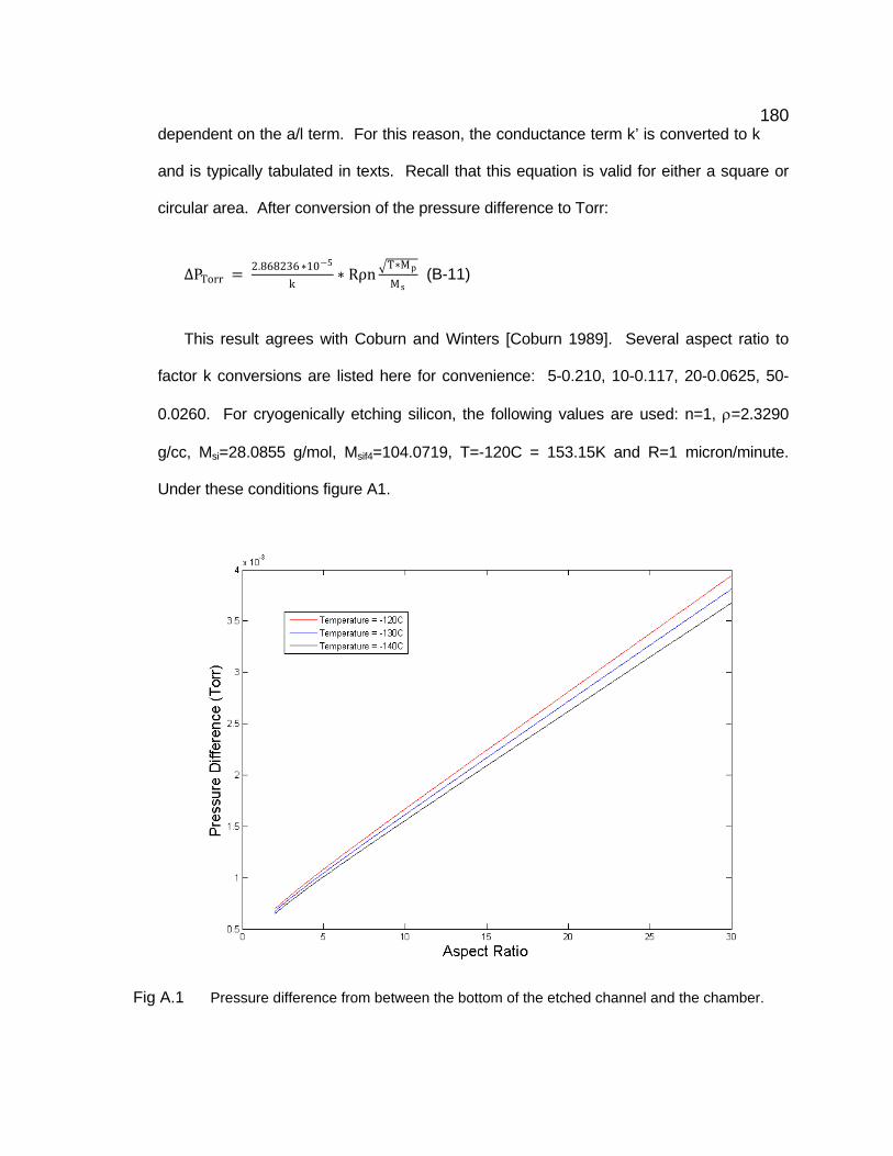
180 dependent on the a/l term. For this reason, the conductance term k’ is converted to k
and is typically tabulated in texts. Recall that this equation is valid for either a square or
circular area. After conversion of the pressure difference to Torr:
ΔPTorr = 2.868236 ∗10−5
k∗ Rρn T∗Mp
Ms (B-11)
This result agrees with Coburn and Winters [Coburn 1989]. Several aspect ratio to
factor k conversions are listed here for convenience: 5-0.210, 10-0.117, 20-0.0625, 50-
0.0260. For cryogenically etching silicon, the following values are used: n=1, ρ=2.3290
g/cc, Msi=28.0855 g/mol, Msif4=104.0719, T=-120C = 153.15K and R=1 micron/minute.
Under these conditions figure A1.
Fig A.1 Pressure difference from between the bottom of the etched channel and the chamber.

181 Although the high aspect ratio trenches do indeed build up a pressure difference,
this is only part of the problem. Calculation of the mean free path of the SiF4 gas particle
should be looked at as well. Further, Knudsen relied on the assumption that the pressure
was significantly low enough for the system to be under molecular flow. So looking at the
mean free path assuming a Maxwellian distribution:
𝑠𝑠 = 𝐾𝐾𝐵𝐵𝑇𝑇√2𝜋𝜋𝑃𝑃2𝑃𝑃
(B-12)
Where d is the diameter of the gas molecule, approximately 200 pm for SiF4, and P is
the pressure of the system. Under these approximations the mean free path of the etch
product in 10 mTorr is 22.3 cm. This implied that the addition of 4 mTorr will not act as a
significant pressure to scatter outgoing or incoming molecules (radicals or neutrals).
Appendix C – Notching Effect in Cryogenic Etching Notching is what is referred to when a gentile curvature exists at the top of a
cryogenically etched structure. This notching can limit the etch height of very small
features, such as a 5 micron diameter pillar, well before the etch mask begins eroding.
This notching is not the same as lateral etching, where the entire etched wall is etched
horizontally, but instead is characterized by very straight and vertical sidewall except for
the top few microns of the structure.
Fig A.2 Scanning electron micrographs of 5 micron width silicon ridges. The left image was a
silicon ridge 5.105 microns wide, 530 nm undercut, and etched for 20 min, middle was a silicon ridge 5.018 microns, 1.165 microns, and 40 min, and the right image was a silicon ridge 5.338 microns, 2.1495 microns, and 60 minutes.

182
To date, the exact nature of notching is unknown. Two possible candidates are IADF
and localized heating. Since IADF implies that there will always be some lateral etching
due to ions approaching the surface with some parallel velocity vector, as the trench
aspect ratio increases the number of ions with lateral velocity vectors striking the sidewall
decreases. For this reason, an hour glass shape is expected at the top of the sidewall.
Localized heating refers to the fact that the top of the etched structure is exposed to a
constant thermal flux from the plasma. This thermal flux is expected to transit through the
silicon to the cooled etch table. If the surface area of the etched structure is small, then as
the etch height increases the thermal resistance also increases. To accommodate a
constant flux of thermal energy, this implies that the temperature at the top of the etched
structure should rise in temperature. A rise in temperature has been demonstrated earlier
to reduce the passivation which could explain the hourglass shape. This phenomenon is
unique to cryogenic etching; in fact for the same DC bias this notching does not arise with
the pseudo Bosch etching. Since both etches are based on passivation, it is hypothesized
that the basis of the notching is due to the thin SiOxFy passivation layer.
Thermal heating is caused by 2 basic events: ionic bombardment energy flux and
chemical reaction heating from the etching process. Since this problem is based on the
idea that the heating starts at the top of the etched structure, it is assumed that there is no
chemical reaction occurring with the etch mask and impinging ions. To calculate the ion
bombardment flux, one assumes that the SiF4 leaving a Si carrier wafer (unmasked) is due
to F ions impinging on the surface. Based on the fact that the cryogenic etch is more
radial etching and less ion etching, this assumption over accounts in energy by a factor of
several thousand. This over account of the ion flux will generate a higher than actual
temperature, but as it will be seen to be navigable. For a given etch rate, the number of
incoming fluorine ions is calculated to:
𝐺𝐺𝑆𝑆𝑐𝑐𝐹𝐹4 =𝑅𝑅 ∗ 𝑑𝑑 ∗ 𝜌𝜌𝑠𝑠𝑐𝑐
𝑀𝑀𝑆𝑆𝑐𝑐
Where R is the etch rate, A is the area of the wafer, ρsi is the density of silicon and Msi
is the molar weight of silicon. Then by associating all the fluorine flux attacking the surface
as the ion flux is:

183
𝐽𝐽𝐹𝐹𝑐𝑐𝑐𝑐𝐿𝐿𝑠𝑠 = 4 ∗𝑅𝑅[𝜇𝜇𝑐𝑐𝑐𝑐𝑐𝑐𝑐𝑐𝐿𝐿𝑠𝑠𝜇𝜇𝑐𝑐𝐿𝐿 ]
6 ∗ 105[𝜇𝜇𝑐𝑐𝑐𝑐𝑐𝑐𝐿𝐿𝑠𝑠 𝑠𝑠𝑚𝑚𝑐𝑐min 𝑐𝑐𝜇𝜇 ]
∗𝜌𝜌𝑠𝑠𝑐𝑐 [
𝑔𝑔𝑐𝑐𝜇𝜇3]
𝑀𝑀𝑆𝑆𝑐𝑐 [𝑔𝑔𝜇𝜇𝑐𝑐𝑠𝑠]
∗ 𝑁𝑁𝑑𝑑 𝑐𝑐𝑐𝑐𝐿𝐿𝑠𝑠𝜇𝜇𝑐𝑐𝑠𝑠
∗ 𝑞𝑞[𝐶𝐶𝑐𝑐𝑐𝑐𝐿𝐿
]
Calculation of the ionic bombardment energy flux is: 𝐻𝐻
𝑑𝑑𝑐𝑐𝑚𝑚𝑎𝑎= 𝐽𝐽𝐹𝐹𝑐𝑐𝑐𝑐𝐿𝐿𝑠𝑠 ∗ 𝑉𝑉𝐷𝐷𝐶𝐶 𝐵𝐵𝑐𝑐𝑎𝑎𝑠𝑠
Then using Newton’s Law of cooling:
𝐻𝐻 =𝑃𝑃𝑄𝑄𝑃𝑃𝑑𝑑
= 𝑘𝑘 ∗ 𝑑𝑑 ∗𝑃𝑃𝑇𝑇𝑃𝑃𝐸𝐸
𝐻𝐻𝑑𝑑
= 𝑘𝑘 ∗𝑃𝑃𝑇𝑇𝑃𝑃𝐸𝐸
Substitution of the energy flux into the equation: 𝑃𝑃𝑇𝑇𝑃𝑃𝐸𝐸
=𝐽𝐽𝐹𝐹𝑐𝑐𝑐𝑐𝐿𝐿𝑠𝑠 ∗ 𝑉𝑉𝐷𝐷𝐶𝐶 𝐵𝐵𝑐𝑐𝑎𝑎𝑠𝑠
𝑘𝑘
For a 1.14 micron per minute etch rate, the ion current density is 61 mA per cm2.
Using a DC Bias of 40 volts, the energy flux is 2.44 W per cm2. This means that the
vertical temperature change along an etched structure per micron is 0.165*10-3 C per
micron. This would not be enough to affect the passivation, hence the likely explanation
for the undercutting is IADF.

184 Appendix D – Mathematica Code for Microcoil Calculations

185
Appendix E – Effect of Point Contacts on Resistance This calculation was first performed as a homework problem I had for an
electromagnetic physics coarse and the problem hypothetical. However, the theoretical
framework is quite powerful and versatile. After spending time in industry trying to
calculate how the location of where bond wires attach to a semiconductor can change the
intended resistance, I realized at once that this was the method to achieve a closed form
solution I was looking for. This answer can also serve as what happens when a probe tip
makes contact on a wire run, or if wire runs change from very thin to thick wire runs. At
the end of this appendix, modifications are discussed for using the solutions for
applicability to silicon nanowires.
Begin with the basic electrostatic equations:
∇ × 𝐸𝐸 = 0 ,𝐸𝐸 = 𝜌 ∙ 𝐽𝐽 ,∇ ∙ J = 0
Then if we assume the sheet is a essentially a surface current, requiring the
assumption that it is longer and wider than it is thick, then J is replaced with a K/t (the t will
be implicit regarding the symbol K). At this point a φ is created, in a similar fashion as one
might define a fictitious vector potential, and utilized in the equations:
𝑧 × ∇𝜙𝜙 = 𝐾𝐾 = −𝜕𝜕𝑠𝑠𝜙𝜙𝐸𝐸 + 𝜕𝜕𝐸𝐸𝜙𝜙𝑠𝑠
∇ × 𝐸𝐸 = (𝜕𝜕𝐸𝐸𝐸𝐸𝑠𝑠 − 𝜕𝜕𝑠𝑠𝐸𝐸𝐸𝐸)𝑧 = (𝜌𝜌𝑠𝑠 ∙ 𝜕𝜕𝐸𝐸𝐾𝐾𝑠𝑠 − 𝜌𝜌𝐸𝐸 ∙ 𝜕𝜕𝑠𝑠𝐾𝐾𝐸𝐸)𝑧 = 0
𝜌𝜌𝑠𝑠 ∙ 𝜕𝜕𝐸𝐸2𝜙𝜙 + 𝜌𝜌𝐸𝐸 ∙ 𝜕𝜕𝑠𝑠2𝜙𝜙 = 0
This 2-D partial differential equation is solvable by separation of variables, φ=f(x)*g(y):

186
−𝜌𝜌𝐸𝐸𝜌𝜌𝑠𝑠∙
1𝑔𝑔𝜕𝜕𝑠𝑠2𝑔𝑔 =
1𝑓𝑓𝜕𝜕𝐸𝐸2𝑓𝑓 = −𝜇𝜇2
The solutions to the now ordinary differential equations are also classical:
𝑓𝑓(𝐸𝐸) = 𝑐𝑐3 Sin(𝜇𝜇𝐸𝐸) + 𝑐𝑐4 Cos(𝜇𝜇𝐸𝐸)
𝑔𝑔(𝑠𝑠) = 𝑐𝑐1 Sinh𝜌𝜌𝑠𝑠𝜌𝜌𝐸𝐸𝜇𝜇𝑠𝑠 + 𝑐𝑐2 Cosℎ
𝜌𝜌𝑠𝑠𝜌𝜌𝐸𝐸𝜇𝜇𝑠𝑠
As with all problems, the interesting things happen when boundary conditions are
applied. Assume that a bond wire connects up at x=0 and y=w/2 and at x=l and y=w/2 for
a sheet that is w wide and l long and the corner of the sheet is situated at x=0. A second
assumption is that the current I is injected from the bond wires.
𝐾𝐾𝐸𝐸(𝐸𝐸 = 0, 𝑠𝑠) = 0 𝑎𝑎𝐿𝐿𝑃𝑃 𝐾𝐾𝑠𝑠(𝑠𝑠 = 0,𝑤𝑤) = 0
𝐾𝐾𝑠𝑠𝛿𝛿 𝐸𝐸 = 0, 𝑠𝑠,𝑠𝑠 =𝑤𝑤2 = −
𝐼𝐼2𝑎𝑎𝐿𝐿𝑃𝑃 𝐾𝐾𝐸𝐸 ∙ 𝛿𝛿(𝐸𝐸 = 0, 𝑠𝑠,𝑠𝑠 =
𝑤𝑤2
) = −𝐼𝐼
Translating the BC for the vector potential gives:
𝜕𝜕𝑠𝑠𝜙𝜙(𝐸𝐸 = 0, 𝑠𝑠) = 0 𝑎𝑎𝐿𝐿𝑃𝑃 𝜕𝜕𝐸𝐸𝜙𝜙(𝑠𝑠 = 0,𝑤𝑤) = 0
𝑓𝑓(𝐸𝐸 = 0) = 0 + 𝑐𝑐4 Cos(𝜇𝜇𝐸𝐸) = 0, 𝑠𝑠𝑐𝑐 𝑐𝑐4 = 0
𝑓𝑓(𝐸𝐸 = 𝑠𝑠) = 𝑐𝑐3 Sin(𝜇𝜇𝑠𝑠) = 0, 𝑠𝑠𝑐𝑐 𝜇𝜇 =𝐿𝐿𝜋𝜋𝑠𝑠
𝑓𝑓𝑐𝑐𝑐𝑐 𝐿𝐿 = 0,1,2 …
𝑔𝑔(𝑠𝑠 = 0) = 0 + 𝑐𝑐2 Cosℎ(0) = 0, 𝑠𝑠𝑐𝑐 𝑐𝑐2 = 0
Looking at the delta function with some symmetry (half the current flows upward and
half the current flows downward at y=w/2 at the contact),
∫ 𝐾𝐾𝐸𝐸𝑤𝑤2
0 𝑃𝑃𝐸𝐸 = − 𝐼𝐼2
𝑐𝑐𝜇𝜇𝑠𝑠𝑠𝑠𝑐𝑐𝑚𝑚𝑠𝑠 𝑓𝑓(𝐸𝐸)𝑔𝑔 𝑠𝑠 = 𝑤𝑤2 = − 𝐼𝐼
2
So,
𝑔𝑔 𝑠𝑠 =𝑤𝑤2 = −
𝐼𝐼2
= 𝑐𝑐1 Sinh𝜌𝜌𝑠𝑠𝜌𝜌𝐸𝐸𝐿𝐿𝜋𝜋𝑠𝑠𝑤𝑤2 , 𝑠𝑠𝑐𝑐 𝑐𝑐1 = −
𝐼𝐼
2 Sinh𝜌𝜌𝑠𝑠𝜌𝜌𝐸𝐸𝐿𝐿𝜋𝜋𝑠𝑠𝑤𝑤2
And hence,

187
𝜙𝜙(𝐸𝐸,𝑠𝑠) = −𝑐𝑐3 Sin 𝐿𝐿𝜋𝜋𝑠𝑠𝐸𝐸 ∙
𝐼𝐼 ∙ Sinh𝜌𝜌𝑠𝑠𝜌𝜌𝐸𝐸𝐿𝐿𝜋𝜋𝑠𝑠 𝑠𝑠
2Sinh𝜌𝜌𝑠𝑠𝜌𝜌𝐸𝐸𝐿𝐿𝜋𝜋𝑠𝑠𝑤𝑤2
Since there could be an infinite number of solutions to satisfy φ,
𝜙𝜙(𝐸𝐸,𝑠𝑠) = 𝑐𝑐𝐿𝐿 Sin 𝐿𝐿𝜋𝜋𝑠𝑠𝐸𝐸 ∙
Sinh𝜌𝜌𝑠𝑠𝜌𝜌𝐸𝐸𝐿𝐿𝜋𝜋𝑠𝑠 𝑠𝑠
Sinh𝜌𝜌𝑠𝑠𝜌𝜌𝐸𝐸𝐿𝐿𝜋𝜋𝑠𝑠𝑤𝑤2𝐿𝐿
𝜙𝜙 𝐸𝐸,𝑠𝑠 =𝑤𝑤2 = cnSin
𝐿𝐿𝜋𝜋𝑠𝑠𝐸𝐸
𝐿𝐿
= −𝐼𝐼2
Now applying Fourier’s trick (multiply both sides by a similar Sin function and integrating
over the space):
cnSin 𝐿𝐿𝜋𝜋𝑠𝑠𝐸𝐸
𝐿𝐿
𝑠𝑠
0∙ Sin
𝜇𝜇𝜋𝜋𝑠𝑠𝐸𝐸 𝑃𝑃𝐸𝐸 = −
𝐼𝐼2∙ Sin
𝜇𝜇𝜋𝜋𝑠𝑠𝐸𝐸
𝑠𝑠
0𝑃𝑃𝐸𝐸
cm ∙l2
= −𝐼𝐼2∙𝑠𝑠𝜇𝜇𝜋𝜋
(𝐶𝐶𝑐𝑐𝑠𝑠(𝜇𝜇𝜋𝜋) − 1)
cm =I
mπ1 − 𝐶𝐶𝑐𝑐𝑠𝑠(𝜇𝜇𝜋𝜋)
𝜙𝜙(𝐸𝐸,𝑠𝑠) = I
nπ1 − 𝐶𝐶𝑐𝑐𝑠𝑠(𝐿𝐿𝜋𝜋) ∙ Sin
𝐿𝐿𝜋𝜋𝑠𝑠𝐸𝐸 ∙
Sinh𝜌𝜌𝑠𝑠𝜌𝜌𝐸𝐸𝐿𝐿𝜋𝜋𝑠𝑠 𝑠𝑠
Sinh𝜌𝜌𝑠𝑠𝜌𝜌𝐸𝐸𝐿𝐿𝜋𝜋𝑠𝑠𝑤𝑤2𝐿𝐿
Going back to the surface current:
𝐾𝐾𝐸𝐸 = −𝜕𝜕𝑠𝑠𝜙𝜙
𝐾𝐾𝐸𝐸 = −𝜌𝜌𝑠𝑠𝜌𝜌𝐸𝐸𝐼𝐼𝑠𝑠1 − 𝐶𝐶𝑐𝑐𝑠𝑠(𝜇𝜇𝜋𝜋) ∙ Sin
𝐿𝐿𝜋𝜋𝑠𝑠𝐸𝐸 ∙
Cosh𝜌𝜌𝑠𝑠𝜌𝜌𝐸𝐸𝐿𝐿𝜋𝜋𝑠𝑠 𝑠𝑠
Sinh𝜌𝜌𝑠𝑠𝜌𝜌𝐸𝐸𝐿𝐿𝜋𝜋𝑠𝑠𝑤𝑤2𝐿𝐿
Now finding the voltage drop across the sheet (note that t is the thickness of the sheet to
convert from J to K/t:

188
𝑉𝑉 = − 𝐸𝐸𝐸𝐸 ∙ 𝑃𝑃𝐸𝐸𝑠𝑠
0= 𝜌𝜌𝐸𝐸 ∙
1𝑑𝑑∙
𝜌𝜌𝑠𝑠𝜌𝜌𝐸𝐸𝐼𝐼𝑠𝑠1 − 𝐶𝐶𝑐𝑐𝑠𝑠(𝜇𝜇𝜋𝜋) ∙ Sin
𝐿𝐿𝜋𝜋𝑠𝑠𝐸𝐸 ∙
Cosh𝜌𝜌𝑠𝑠𝜌𝜌𝐸𝐸𝐿𝐿𝜋𝜋𝑠𝑠𝑤𝑤2
Sinh𝜌𝜌𝑠𝑠𝜌𝜌𝐸𝐸𝐿𝐿𝜋𝜋𝑠𝑠𝑤𝑤2𝐿𝐿
𝑃𝑃𝑠𝑠𝑠𝑠
0
𝑉𝑉 = 1
nπ∙
1𝑑𝑑∙ 𝜌𝜌𝐸𝐸𝜌𝜌𝑠𝑠 ∙ 𝐼𝐼 ∙ (1 − Cos(𝐿𝐿𝜋𝜋))2 ∙
Cosh𝜌𝜌𝑠𝑠𝜌𝜌𝐸𝐸𝐿𝐿𝜋𝜋𝑠𝑠𝑤𝑤2
Sinh𝜌𝜌𝑠𝑠𝜌𝜌𝐸𝐸𝐿𝐿𝜋𝜋𝑠𝑠𝑤𝑤2𝐿𝐿
Dividing by the injected current yields the resistance:
𝑅𝑅 = 1𝐿𝐿𝜋𝜋
∙1𝑑𝑑∙ 𝜌𝜌𝐸𝐸𝜌𝜌𝑠𝑠 ∙
(1 − Cos(𝐿𝐿𝜋𝜋))2
Tanh𝜌𝜌𝑠𝑠𝜌𝜌𝐸𝐸𝐿𝐿𝜋𝜋𝑠𝑠𝑤𝑤2𝐿𝐿
The function of the t in the equation, serves to change the sheet resistance to a
resistance. Comparison of the modified resistance to what was expected and assuming
an isotropic resistivity:
∆𝑅𝑅 = (1𝐿𝐿𝜋𝜋
∙1𝑑𝑑∙ 𝜌𝜌 ∙
(1 − Cos(𝐿𝐿𝜋𝜋))2
Tanh𝜌𝜌𝑠𝑠𝜌𝜌𝐸𝐸𝐿𝐿𝜋𝜋𝑠𝑠𝑤𝑤2𝐿𝐿
) −𝜌𝜌𝑠𝑠𝑑𝑑𝑤𝑤
𝑚𝑚𝑐𝑐𝑐𝑐𝑐𝑐𝑐𝑐 𝑓𝑓𝑎𝑎𝑐𝑐𝑑𝑑𝑐𝑐𝑐𝑐 =∆𝑅𝑅𝑅𝑅
= 1
𝐿𝐿𝜋𝜋 ∙ 𝑑𝑑𝑅𝑅∙
(1 − Cos(𝐿𝐿𝜋𝜋))2
Tanh 𝐿𝐿𝜋𝜋2 ∙ 𝑑𝑑𝑅𝑅𝐿𝐿
− 1
Fig A.3 Plot of error factor in resistance (delta R / R) due to contacting the structure with a point contact. As the aspect ratio gets large, the effect of the contact diminishes quickly.
189 BIBLIOGRAPHY
[1] M. Sugawara, Plasma etching: fundamentals and applications, New York: Oxford University Press Inc, 1998.
[2] H. Jansen, M. de Boer, S. Unnikrishnan, M. Louwerse, and M.C. Elwenspoek, "Black silicon method X : a review on high speed and selective plasma etching of silicon with profile control : an in-depth comparison between Bosch and cryostat DRIE processes as a roadmap to next generation equipment," Journal of Micromechanics and Microengineering, vol. 19, 2009, pp. 1-41.
[3] V. Hodoroaba, V. Hoffmann, E.B. Steers, and K. Wetzig, "Emission spectra of copper and argon in an argon glow discharge containing small quantities of hydrogen," Journal of Analytical Atomic Spectrometry, vol. 15, 2000, pp. 951-958.
[4] C. Welch, a. Goodyear, G. Ditmer, and G. Tan, "Choice of Silicon Etch Processes for Opto- and Microelectronic Device Fabrication Using Inductively Coupled Plasmas," Conference on Optoelectronic and Microelectronic Materials and Devices, 2004., 2005, pp. 13-16.
[5] X. Li, L. Ling, X. Hua, M. Fukasawa, G.S. Oehrlein, M. Barela, and H.M. Anderson, "Effects of Ar and O 2 additives on SiO 2 etching in C 4 F 8 -based plasmas," J. Vac. Sci. Technol. A, vol. 21, 2003, pp. 284-293.
[6] H. Rhee, H. Kwon, and C. Kim, "Comparison of deep silicon etching using SF 6 / C 4 F 8 and SF 6 / C 4 F 6 plasmas in the Bosch process," J. Vac. Sci. Technol. B, vol. 26, 2008, pp. 576-581.
[7] S. Tachi, K. Tsujimoto, and S. Okudaira, "Low temperature reactive ion etching and microwave plasma etching of silicon," Engineering, 1987, pp. 616-618.
[8] M.a. Blauw, E. van der Drift, G. Marcos, and a. Rhallabi, "Modeling of fluorine-based high-density plasma etching of anisotropic silicon trenches with oxygen sidewall passivation," Journal of Applied Physics, vol. 94, 2003, p. 6311.
[9] X. Mellhaoui, R. Dussart, T. Tillocher, P. Lefaucheux, and P. Ranson, "SiO x F y passivation layer in silicon cryoetching," Journal of Applied Physics, vol. 98, 2005, pp. 1-10.
[10] a.F. Isakovic, K. Evans-Lutterodt, D. Elliott, a. Stein, and J.B. Warren, "Cyclic, cryogenic, highly anisotropic plasma etching of silicon using SF[sub 6]∕O[sub 2],"

190 Journal of Vacuum Science & Technology A: Vacuum, Surfaces, and Films, vol. 26, 2008, p. 1182.
[11] J. Karttunen, S. Franssila, and J. Kiihama, "Etching through silicon wafer in inductively coupled plasma," Microsystem Technologies, vol. 6, 2000, pp. 141-144.
[12] M.J. Boer, J.G. Gardeniers, H.V. Jansen, E. Smulders, M. Gilde, G. Roelofs, J.N. Sasserath, M. Elwenspoek, and A. Member, "Guidelines for Etching Silicon MEMS Structures Using Fluorine High-Density Plasmas at Cryogenic Temperatures," Journal of Microelectromechanical Systems, vol. qqq, 2002, pp. 385-401.
[13] M.D. Henry, C. Welch, and A. Scherer, "Techniques of cryogenic reactive ion etching in silicon for fabrication of sensors," Journal of Vacuum Science & Technology A: Vacuum, Surfaces, and Films, vol. 27, 2009, p. 1211.
[14] J. Yeom, Y. Wu, J.C. Selby, and M.a. Shannon, "Maximum achievable aspect ratio in deep reactive ion etching of silicon due to aspect ratio dependent transport and the microloading effect," Journal of Vacuum Science & Technology B: Microelectronics and Nanometer Structures, vol. 23, 2005, p. 2319.
[15] I. Rangelow, "Critical tasks in high aspect ratio silicon dry etching for microelectromechanical systems," J. Vac. Sci. Technol. A, vol. 21, 2003, pp. 1550-1562.
[16] R.a. Gottscho, "Microscopic uniformity in plasma etching," Journal of Vacuum Science & Technology B: Microelectronics and Nanometer Structures, vol. 10, 1992, p. 2133.
[17] J.W. Coburn and H.F. Winters, "Conductance considerations in the reactive ion etching of high aspect ratio features," Applied Physics Letters, vol. 55, 1989, p. 2730.
[18] S. Dushman, Scientific Foundations of Vacuum Technique, New York: Wiley and Sons Inc, 1949.
[19] H. Rhee, H.M. Lee, Y.M. Namkoung, C. Kim, H. Chae, and Y.W. Kim, "Dependence of etch rates of silicon substrates on the use of C[sub 4]F[sub 8] and C[sub 4]F[sub 6] plasmas in the deposition step of the Bosch process," Journal of Vacuum Science & Technology B: Microelectronics and Nanometer Structures, vol. 27, 2009, p. 33.

191 [20] Y. Chen, Z. Li, M.D. Henry, and A. Scherer, "Optofluidic circular grating
distributed feedback dye laser," Applied Physics Letters, vol. 95, 2009, p. 031109.
[21] B.M. Kayes, H.A. Atwater, and N.S. Lewis, "Comparison of the device physics principles of planar and radial p-n junction nanorod solar cells," Journal of Applied Physics, vol. 97, 2005, pp. 1-11.
[22] N. Singh, A. Agarwal, L.K. Bera, T.Y. Liow, R. Yang, S.C. Rustagi, C.H. Tung, R. Kumar, G.Q. Lo, N. Balasubramanian, and D. Kwong, "High-Performance Fully Depleted Silicon Nanowire ( Diameter ≤ 5 nm ) Gate-All-Around CMOS Devices," IEEE ELECTRON DEVICE LETTERS, vol. 27, 2006, pp. 383-386.
[23] U. Sokmen, A. Stranz, S. Fundling, H. Wehmann, V. Bandalo, A. Bora, M. Tornow, A. Waag, and E. Peiner, "Capabilities of ICP-RIE cryogenic dry etching of silicon : review of exemplary microstructures," J. Micromech. Microeng, vol. 19, 2009, pp. 1-8.
[24] V. Bakshi, EUV Lithography, Bellingham: SPIE, 2009.
[25] L. Sainiemi and S. Franssila, "Mask material effects in cryogenic deep reactive ion etching," J. Vac. Sci. Technol. B, vol. 25, 2007, pp. 801-807.
[26] K.R. Williams, S. Member, K. Gupta, S. Member, and M. Wasilik, "Etch Rates for Micromachining Processing — Part II," Journal of Microelectromechanical Systems, vol. 12, 2003, pp. 761-778.
[27] J. Ziegler, J. Biersack, and U. Littmark, The stopping and range of ions in solids, New York: Pergamon, 1985.
[28] N.I. Kato, Y. Kohno, and H. Saka, "Side-wall damage in a transmission electron microscopy specimen of crystalline Si prepared by focused ion beam etching," J. Vac. Sci. Technol. A, vol. 17, 1999, pp. 1201-1204.
[29] A.A. Tseng, "Recent developments in micromilling using focused ion beam technology," J. Micromech. Microeng, vol. 14, 2004, pp. R15-R34.
[30] J. Gierak, D. Mailly, P. Hawkes, R. Jede, L. Bruchhaus, L. Bardotti, B. Prevel, P. Melinon, A. Perez, R. Hyndman, J. Jamet, J. Ferre, A. Mougin, C. Chappert, V. Mathet, P. Warin, and J. Chapman, "Exploration of the ultimate patterning potential achievable with high resolution focused ion beams," Applied Physics A, vol. 80, 2005, pp. 187-194.

192 [31] K. Arshak, M. Mihov, S. Nakahara, A. Arshak, and D. Mcdonagh, "A novel
focused-ion-beam lithography process for sub-100 nanometer technology nodes," Superlattices and Microstructures, vol. 36, 2004, pp. 335-343.
[32] F. Watt, A. Bettiol, J.A. Van Kan, E.J. Teo, and M.B. Breese, "ION BEAM LITHOGRAPHY AND NANOFABRICATION : A REVIEW," International Journal of Nanoscience, vol. 4, 2005, pp. 269-286.
[33] B. Schmidt, S. Oswald, and L. Bischoff, "Etch Rate Retardation of Ga + -Ion Beam-Irradiated Silicon," Journal of The Electrochemical Society, vol. 152, 2005, pp. 875-879.
[34] N. Chekurov, K. Grigoras, A. Peltonen, and S. Franssila, "The fabrication of silicon nanostructures by local gallium implantation and cryogenic deep reactive ion etching," Nanotechnology, vol. 20, 2009, pp. 1-5.
[35] H.X. Qian, W. Zhou, J. Miao, L.E. Lim, and X.R. Zeng, "Fabrication of Si microstructures using focused ion beam implantation and reactive ion etching," J. Micromech. Microeng, vol. 18, 2008.
[36] L. Mosher, C.M. Waits, S. Member, B. Morgan, R. Ghodssi, and A. A, "Double-Exposure Grayscale Photolithography," vol. 18, 2009, pp. 308-315.
[37] A.A. Tseng, I.A. Insua, J.S. Park, B. Li, and G.P. Vakanas, "Milling of submicron channels on gold layer using double charged arsenic ion beam," J. Vac. Sci. Technol. B, vol. 22, 2004, pp. 82-89.
[38] L. Frey, C. Lehrer, and H. Ryssel, "Nanoscale effects in focused ion beam processing," Applied Physics A: Materials Science & Processing, vol. 76, 2003, pp. 1017-1023.
[39] M.K. Sunkara, S. Sharma, R. Miranda, G. Lian, and E.C. Dickey, "Bulk synthesis of silicon nanowires using a low-temperature vapor–liquid–solid method," Applied Physics Letters, vol. 79, 2001, p. 1546.
[40] M. Borselli, T.J. Johnson, C.P. Michael, M.D. Henry, and O. Painter, "Surface encapsulation for low-loss silicon photonics," Applied Physics Letters, vol. 91, 2007, p. 131117.
[41] F.A. Padovani and R. Stratton, "Field and thermionic-field emission in Schottky barriers," Solid-State Electronics, vol. 9, 1966, p. 695.
[42] S. Sze and K. NG, Physics of Semiconductor Devices, Hoboken: Wiley and Sons Inc, 2007.

193 [43] R.W. Olesinski, N. Kanani, and G.J. Abbaschian, "The Ga−Si (Gallium-
Silicon) system," Bulletin of Alloy Phase Diagrams, vol. 6, 1985, pp. 362-364.
[44] a. Schilling, T. Adams, R.M. Bowman, and J.M. Gregg, "Strategies for gallium removal after focused ion beam patterning of ferroelectric oxide nanostructures.," Nanotechnology, vol. 18, 2007, p. 035301.
[45] R.L. Macin, A.C. Webb, and T.L. Peck, "Miniature magnetic resonance machines," Ieee Spectrum, 1997, pp. 51-61.
[46] G. Moresi and R. Magin, "Miniature permanent magnet for table-top," NMR, Concepts Magn. Reson. B, vol. 19, 2003, p. 35.
[47] F.D. Doty, G. Entzminger, and Y.A. Yang, "Magnetism in High-Resolution NMR Probe Design . I : General Methods," Concepts In Magnetic Resonance, vol. 10, 1998, pp. 133-156.
[48] H.S. Lopez, F. Liu, E. Weber, and S. Crozier, "Passive Shim Design and a Shimming Approach for Biplanar Permanent Magnetic Resonance Imaging Magnets," IEEE Transactions on Magnetics, vol. 44, 2008, pp. 394-402.
[49] D.J. Griffiths, Introduction to Electrodynamics, New Jersey: Prentice Hall, 1999.
[50] S. Attwood, Electric and Magnetic Fields, London: Wiley and Sons Inc, 1941.
[51] L.R. Moskowitz, Permanent Magnet Design and Application Handbook, Krieger Publishing Co, 1995.
[52] P. Campbell, Permanent Magnet Materials and their Application, Cambridge University Press, 1996.
[53] Z. Liang and P.C. Lauterbur, Principles of Magnetic Resonance Imaging: a Signal Processing Perspective, New York: IEEE Press, 2000.
[54] J.S. Marsh, The alloys of iron and nickel..., New York: McGraw-Hill, 1938.
[55] M. Takahashi, "Induced Magnetic Anisotropy of Evaporated Films Formed in a Magnetic Field," Journal of Applied Physics, vol. 33, 1962, pp. 1351-1352.
[56] A. Sunderland, L. Ju, D.G. Blair, W. Mcrae, and H. Golden, "Low magnetic susceptibility materials and applications in magnetic gradiometry," Smart Materials and Structures, vol. 095038, 2009, p. 095038.

194 [57] J. Mispelter, L. Mihaela, and A. Briguet, NMR Probeheads for Biophysical
and Biomedical Experiments: Theoretical Principles and Practical Guidelines, London: Imperial College Press, 2006.
[58] K. Ehrmann, M. Gersbach, P. Pascoal, F. Vincent, C. Massin, and D. Stamou, "Sample patterning on NMR surface microcoils," Journal of Magnetic Resonance, vol. 178, 2006, pp. 96-105.
[59] C. Massin, F. Vincent, A. Homsy, K. Ehrmann, G. Boero, P. Besse, A. Daridon, E. Verpoorte, N.F. Rooij, and R.S. Popovic, "Planar microcoil-based microfluidic NMR probes," Journal of Magnetic Resonance, vol. 164, 2003, pp. 242-255.
[60] M. Brunet, T. O’donnell, J. O’brien, P. Mccloskey, and S.C. Mathuna, "Thick photoresist development for the fabrication of high aspect ratio magnetic coils," J. Micromech. Microeng, vol. 12, 2002, pp. 444-449.
[61] S. Eroglu, B. Gimi, B. Roman, G. Friedman, and R.L. Magin, "NMR Spiral Surface Microcoils : Design , Fabrication , and Imaging," Concepts In Magnetic Resonance Part B, vol. 17B, 2003, pp. 1-10.
[62] Y. Li, M.M. Ahmad, J.W. Hand, R.R. Syms, D. Gilderdale, D.J. Collins, and I.R. Young, "Microcoils on Structured Silicon Substrates for Magnetic Resonance Detection," IEEE Sensors Journal, vol. 7, 2007, pp. 1362-1369.
[63] T. Pan, A. Baldi, E. Davies-venn, R.F. Drayton, and B. Ziaie, "Fabrication and modeling of silicon-embedded high-Q inductors," Journal of Micromechanics and Microengineering, vol. 15, 2005, pp. 849-854.
[64] M. Lany, G. Boero, and R.S. Popovic, "Superparamagnetic microbead inductive detector," Review of Scientific Instruments, vol. 76, 2005, pp. 1-4.
[65] J. Wang, A. Reykowski, and J. Dickas, "Calculation of the Signal-to-Noise Ratio for Simple Surface Coils and Arrays of Coils," IEEE Transactions on Biomedical Engineering, vol. 42, 1995, pp. 908-917.
[66] T.P. Meyrath, "Electromagnet Design Basics for Cold Atom Experiments," vol. 2, 2004, pp. 1-13.
[67] T. Chen, J.D. Deng, C. Lee, and C. Kao, "Improved Performance of Si-Based Spiral Inductors," IEEE Microwave and Wireless Components Letters, vol. 14, 2004, pp. 466-468.