ieee journal of solid-state circuits, vol. 42, …nansun/resources/nansun_soliton_jssc.pdf · on...
TRANSCRIPT
IEEE JOURNAL OF SOLID-STATE CIRCUITS, VOL. 42, NO. 8, AUGUST 2007 1657
On the Self-Generation of Electrical Soliton PulsesDavid S. Ricketts, Member, IEEE, Xiaofeng Li, Student Member, IEEE, Nan Sun, Student Member, IEEE,
Kyoungho Woo, Student Member, IEEE, and Donhee Ham, Member, IEEE
Abstract—The nonlinear transmission line is a structure whereshort-duration pulses called electrical solitons can be createdand propagated. By combining, in a closed-loop topology, thenonlinear line and a special amplifier that provides not only gainbut also mechanisms to tame inherently unruly soliton dynamics,we recently constructed the first electrical soliton oscillator thatself-generates a stable, periodic train of electrical soliton pulses(Ricketts et al., IEEE Trans. MTT, 2006). This paper starts witha review of this recently introduced circuit concept, and thenreports on new contributions, i.e., further experimental studies ofthe dynamics of the stable soliton oscillator and a CMOS proto-type demonstrating the chip-scale operation of the stable solitonoscillator. Finally, we go to the opposite end of the spectrum andpresent a numerical study showing the possibilities that deliberatepromotions of the unruly soliton dynamics in the closed-looptopology can produce chaotic signals.
Index Terms—Electrical soliton oscillators, electrical solitons,chaos, integrated circuits, mode-locking, nonlinear transmissionlines, oscillators, pulse generation, solitons.
I. INTRODUCTION
SHORT-DURATION electrical pulses play important rolesin ultrafast time-domain metrology: they are used to sample
rapidly varying signals or as probe signals in ranging radarsand time-domain reflectometry [2]–[4]. In addition, possible useof short pulses as career signals in communication has beenactively investigated [5].
The nonlinear transmission line (NLTL), a 1-D lattice ofinductors and varactors [Fig. 1(a)], stands as one of the mostpowerful vehicles to generate short electrical pulses [6]. Thisis due to NLTL’s unique ability to shape an input signal intoa sharp, spatially localized pulse known as a soliton: Fig. 1(a)shows an example where an input pulse is compressed into asoliton. The NLTL has been extensively studied over the past40 years [6]–[8], culminating in a monolithic structure thatcan achieve a pulse rise time as low as 480 fs [8]. In thesepast 40 years of works, however, the NLTL has been usedalmost exclusively as a two-port (input output) device thatrequires a high-frequency input to produce a soliton pulseoutput [Fig. 1(a)].
Manuscript received December 7, 2006; revised March 24, 2007. This workwas supported by the National Science Foundation (NSF) under Grant ECS-0313143 and the Army Research Office (ARO) under Grant W911NF-06-1-0290.
D. S. Ricketts is with the Department of Electrical and Computer Engi-neering, Carnegie Mellon University, Pittsburgh, PA 15232 USA (e-mail:[email protected]).
X. Li, N. Sun, K. Woo, and D. Ham are with Electrical Engineering, School ofEngineering and Applied Sciences, Harvard University, Cambridge, MA 02138USA (e-mail: [email protected]).
Digital Object Identifier 10.1109/JSSC.2007.900291
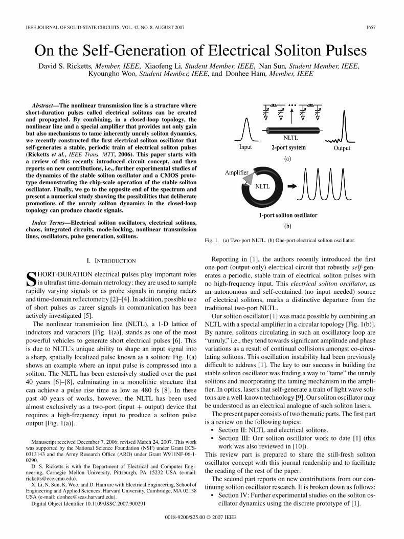
Fig. 1. (a) Two-port NLTL. (b) One-port electrical soliton oscillator.
Reporting in [1], the authors recently introduced the firstone-port (output-only) electrical circuit that robustly self-gen-erates a periodic, stable train of electrical soliton pulses withno high-frequency input. This electrical soliton oscillator, asan autonomous and self-contained (no input needed) sourceof electrical solitons, marks a distinctive departure from thetraditional two-port NLTL.
Our soliton oscillator [1] was made possible by combining anNLTL with a special amplifier in a circular topology [Fig. 1(b)].By nature, solitons circulating in such an oscillatory loop are“unruly,” i.e., they tend towards significant amplitude and phasevariations as a result of continual collisions amongst co-circu-lating solitons. This oscillation instability had been previouslydifficult to address [1]. The key to our success in building thestable soliton oscillator was finding a way to “tame” the unrulysolitons and incorporating the taming mechanism in the ampli-fier. In optics, lasers that self-generate a train of light wave soli-tons are a well-known technology [9]. Our soliton oscillator maybe understood as an electrical analogue of such soliton lasers.
The present paper consists of two thematic parts. The first partis a review on the following topics:
• Section II: NLTL and electrical solitons.• Section III: Our soliton oscillator work to date [1] (this
work was also reviewed in [10]).This review part is prepared to share the still-fresh solitonoscillator concept with this journal readership and to facilitatethe reading of the rest of the paper.
The second part reports on new contributions from our con-tinuing soliton oscillator research. It is broken down as follows:
• Section IV: Further experimental studies on the soliton os-cillator dynamics using the discrete prototype of [1].
0018-9200/$25.00 © 2007 IEEE

1658 IEEE JOURNAL OF SOLID-STATE CIRCUITS, VOL. 42, NO. 8, AUGUST 2007
Fig. 2. (a) An NLTL. (b) Another form of NLTL. (c) The general soliton wave-form on an NLTL.
• Section V: Detailed description of a CMOS prototype thatdemonstrates a chip-scale operation of the soliton oscil-lator. This work was briefly reported in [11].
• Section VI: The focus up to Section V is on attainingstable soliton oscillation by controlling unruly solitons inthe topology of Fig. 1(b). In this section, we explore thepolar opposite, discussing with supporting simulations thecase where promotion of the unruly soliton dynamics inthe same topology leads to chaotic oscillations.
II. REVIEW—NLTL AND ELECTRICAL SOLITONS
A. Solitons
A pulse traveling in a dispersive medium generally breaksdown to multiple sinusoidal waves because different Fouriercomponents propagate at different speeds. Energy initially lo-cally confined in the pulse cannot maintain the spatial localiza-tion as the pulse travels.
In contrast, in a nonlinear dispersive medium, the nonlinearitycan balance out the dispersion, and a unique pulse exhibiting nodispersion can be propagated. This pulse is known as a soliton[12]–[14]. In the absence of loss, the soliton preserves its exactshape while traveling. When loss is present, the soliton changesits shape as it has to lose energy traveling, but it still maintainsspatial localization of energy in the changing pulse shape, notbreaking into multiple sinusoids [15]. Other unique propertiesof solitons will be described shortly in the context of electricalsolitons.
Solitons are encountered throughout nature [16]. Water,plasma, mechanical lattices, optical fibers, and magnetic filmsare examples that can act as nonlinear dispersive media wheresolitons can be propagated in their respective physical forms.
B. Electrical Solitons
In electronics, nonlinear transmission lines (NLTLs) serve asnonlinear dispersive media where electrical solitons can propa-gate in the form of voltage waves [6]. The NLTL is constructedby periodically loading a normal transmission line with varac-tors (e.g., reverse-biased junction diodes or MOS capacitors)[Fig. 2(a)], or alternatively, by arranging inductors and varac-tors in a 1-D lattice [Fig. 2(b)]. The nonlinearity of the NLTLoriginates from the varactors whose capacitance changes with
applied voltage, while its dispersion arises from its structuralperiodicity.
Fig. 2(c) shows the general soliton waveform on an NLTLin the absence of loss, which is a periodic train of voltage soli-tons. This waveform is called the cnoidal wave, and is a solu-tion to what is known as the equation [13]. Many otherphysical manifestations of solitons, e.g., water wave solitons,plasma solitons, and mechanical lattice solitons are solutions tothe equation as well, and the essential properties of elec-trical solitons are common among these -type solitons.1
There are an infinite number of possible cnoidal waves that canform on a given NLTL by interdependently varying amplitude
, pulse spacing , and pulse width [ , , and are withreference to Fig. 2(c)]. Initial or boundary conditions will deter-mine the specific cnoidal wave that can propagate on the NLTL.
Understanding our soliton oscillator, described later, does notwarrant detailed mathematical descriptions of the equa-tion. The following two subsections will rather focus on theirphysical properties pertinent to this paper.
C. Propagation and Collision of Electrical Solitons
In addition to their ability to maintain spatial localizations ofenergy in pulse shapes, electrical solitons on the NLTL exhibitother unique dynamics [12], [13]. Here we review three relevantdynamical properties.
First, a taller soliton travels faster than a shorter one onthe NLTL. Due to this amplitude-dependent speed, if a tallersoliton is placed behind a shorter one [Fig. 3(a), top], the tallerone will catch up and collide with the shorter one, and moveahead of it after the collision [Fig. 3(a)]. Two other impor-tant properties are seen in this collision process. During thecollision [Fig. 3(a), middle], the two solitons do not linearlysuperpose and experience significant amplitude modulations(nonlinear collision). After the collision [Fig. 3(a), bottom],the two solitons recover their original shapes, however, theyhave acquired a permanent time (phase) shift, shown by thedifference between and in Fig. 3(a): with no time shift,
and would be equal since the time elapse before and afterthe collision is the same in the figure. The three soliton prop-erties above, i.e., 1) amplitude-dependent speed, 2) amplitudemodulation during collision, and 3) phase modulation aftercollision, are what makes solitons unruly, and cause difficultiesin constructing a stable soliton oscillator [Section III].
D. Forming and Damping of Electrical Solitons
The previous subsection assumed that electrical solitons werealready formed on the NLTL. How do we form solitons on theNLTL in the first place? If a non-soliton wave is launched ontothe NLTL, it will change its waveform in the course of prop-agation to form into a soliton or solitons [13]. More specifi-cally, a non-soliton input close to soliton shape will be sharp-ened into the soliton while shedding extra energy into a tailringing [Fig. 3(b), top]. A non-soliton input significantly dif-ferent from soliton shape will break up into multiple solitons ofdifferent amplitudes: the bottom of Fig. 3(b) illustrates an ex-ample where a square pulse input on the NLTL breaks up into
1Light wave solitons belong to a different class of solitons [16].

RICKETTS et al.: ON THE SELF-GENERATION OF ELECTRICAL SOLITON PULSES 1659
Fig. 3. (a) Amplitude-dependent soliton speed and nonlinear soliton collisionon an NLTL. d 6= d . (b) Transient soliton-forming processes on an NLTL. (c)Soliton damping on a lossy NLTL.
multiple solitons. It is these transient soliton-forming processes[Fig. 3(b), both top and bottom] that have been widely exploitedfor the past 40 years in the traditional two-port NLTL approachto generate short-duration electrical pulses [6]–[8]. In our one-port soliton oscillator design, the process shown at the top ofFig. 3(b) is beneficial [Section III-D] while the process shownat the bottom of the figure can be detrimental [Section III-B].
Once a soliton is formed through the transient process, it doesnot undergo any further sharpening or breakup. In the absenceof loss, the formed soliton will maintain its exact shape in thecourse of further propagation. When loss is present, the formedsoliton will change its shape as it has to lose energy. The rela-tionships among the amplitude , width , and velocity of anon-damping soliton (a larger corresponds to a larger and asmaller with specific mathematical relations; the – rela-tion is what we previously referred to as amplitude-dependentspeed) are preserved even in the damping soliton, and since thedamping lowers in the course of propagation, the damping
Fig. 4. (a) Soliton oscillator topology. (b) Ring NLTL. Mode 1 (l = �), Mode2 (l = 2�), Mode 3 (l = 3�).
soliton exhibits increasing and decreasing [Fig. 3(c)]: thisunique soliton damping process is well known as reported by Ott[15]. An important notion is that even a damping soliton main-tains spatial localization of energy in its changing pulse shape:the pulse does not break into multiple sinusoids (no dispersion).In addition, damping solitons also retain all the propagation andcollision properties described in Section II-C.
As will be seen in Section III-D, the distinctive dynamics be-tween the soliton damping process (pulse widening) and non-soliton’s soliton-forming transient process (pulse sharpening)provide a criterion to determine when a soliton has actuallyformed on a lossy NLTL.
III. REVIEW—ELECTRICAL SOLITON OSCILLATOR
In this section, we review the basic operating principles of theelectrical soliton oscillator, which we originally reported in [1].This is to familiarize this Journal’s readership with the still-freshsoliton oscillator concept, and to facilitate the reading of thesubsequent sections.
A. Soliton Oscillator Topology
The soliton oscillator consists of a ring NLTL and a non-in-verting amplifier inserted in the ring [Fig. 4(a)]. The ring NLTLsupports certain soliton circulation modes determined by the pe-riodic boundary condition, ( : cir-cumference of the ring NLTL; : spacing between two adjacentsolitons) [Fig. 4(b)]. The amplifier is to enable initial oscilla-tion startup and to compensate loss in steady state (as is com-monly done in sinusoidal oscillators [17], [18]). The ultimategoal of this topology is to self-generate and self-sustain one ofthe soliton circulation modes of Fig. 4(b).
B. Oscillation Instability Mechanisms
The topology indeed leads to oscillations, self-starting fromnoise. However, when standard amplifiers are used in thetopology, the oscillations tend to be plagued with instabilityproblems, exhibiting significant variations in pulse amplitudeand repetition rate [1].
1660 IEEE JOURNAL OF SOLID-STATE CIRCUITS, VOL. 42, NO. 8, AUGUST 2007
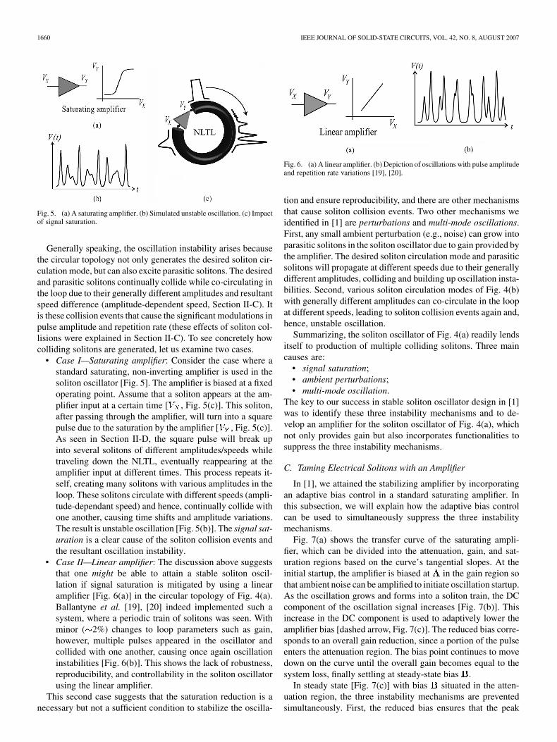
Fig. 5. (a) A saturating amplifier. (b) Simulated unstable oscillation. (c) Impactof signal saturation.
Generally speaking, the oscillation instability arises becausethe circular topology not only generates the desired soliton cir-culation mode, but can also excite parasitic solitons. The desiredand parasitic solitons continually collide while co-circulating inthe loop due to their generally different amplitudes and resultantspeed difference (amplitude-dependent speed, Section II-C). Itis these collision events that cause the significant modulations inpulse amplitude and repetition rate (these effects of soliton col-lisions were explained in Section II-C). To see concretely howcolliding solitons are generated, let us examine two cases.
• Case I—Saturating amplifier: Consider the case where astandard saturating, non-inverting amplifier is used in thesoliton oscillator [Fig. 5]. The amplifier is biased at a fixedoperating point. Assume that a soliton appears at the am-plifier input at a certain time [ , Fig. 5(c)]. This soliton,after passing through the amplifier, will turn into a squarepulse due to the saturation by the amplifier [ , Fig. 5(c)].As seen in Section II-D, the square pulse will break upinto several solitons of different amplitudes/speeds whiletraveling down the NLTL, eventually reappearing at theamplifier input at different times. This process repeats it-self, creating many solitons with various amplitudes in theloop. These solitons circulate with different speeds (ampli-tude-dependant speed) and hence, continually collide withone another, causing time shifts and amplitude variations.The result is unstable oscillation [Fig. 5(b)]. The signal sat-uration is a clear cause of the soliton collision events andthe resultant oscillation instability.
• Case II—Linear amplifier: The discussion above suggeststhat one might be able to attain a stable soliton oscil-lation if signal saturation is mitigated by using a linearamplifier [Fig. 6(a)] in the circular topology of Fig. 4(a).Ballantyne et al. [19], [20] indeed implemented such asystem, where a periodic train of solitons was seen. Withminor ( 2%) changes to loop parameters such as gain,however, multiple pulses appeared in the oscillator andcollided with one another, causing once again oscillationinstabilities [Fig. 6(b)]. This shows the lack of robustness,reproducibility, and controllability in the soliton oscillatorusing the linear amplifier.
This second case suggests that the saturation reduction is anecessary but not a sufficient condition to stabilize the oscilla-
Fig. 6. (a) A linear amplifier. (b) Depiction of oscillations with pulse amplitudeand repetition rate variations [19], [20].
tion and ensure reproducibility, and there are other mechanismsthat cause soliton collision events. Two other mechanisms weidentified in [1] are perturbations and multi-mode oscillations.First, any small ambient perturbation (e.g., noise) can grow intoparasitic solitons in the soliton oscillator due to gain provided bythe amplifier. The desired soliton circulation mode and parasiticsolitons will propagate at different speeds due to their generallydifferent amplitudes, colliding and building up oscillation insta-bilities. Second, various soliton circulation modes of Fig. 4(b)with generally different amplitudes can co-circulate in the loopat different speeds, leading to soliton collision events again and,hence, unstable oscillation.
Summarizing, the soliton oscillator of Fig. 4(a) readily lendsitself to production of multiple colliding solitons. Three maincauses are:
• signal saturation;• ambient perturbations;• multi-mode oscillation.
The key to our success in stable soliton oscillator design in [1]was to identify these three instability mechanisms and to de-velop an amplifier for the soliton oscillator of Fig. 4(a), whichnot only provides gain but also incorporates functionalities tosuppress the three instability mechanisms.
C. Taming Electrical Solitons with an Amplifier
In [1], we attained the stabilizing amplifier by incorporatingan adaptive bias control in a standard saturating amplifier. Inthis subsection, we will explain how the adaptive bias controlcan be used to simultaneously suppress the three instabilitymechanisms.
Fig. 7(a) shows the transfer curve of the saturating ampli-fier, which can be divided into the attenuation, gain, and sat-uration regions based on the curve’s tangential slopes. At theinitial startup, the amplifier is biased at in the gain region sothat ambient noise can be amplified to initiate oscillation startup.As the oscillation grows and forms into a soliton train, the DCcomponent of the oscillation signal increases [Fig. 7(b)]. Thisincrease in the DC component is used to adaptively lower theamplifier bias [dashed arrow, Fig. 7(c)]. The reduced bias corre-sponds to an overall gain reduction, since a portion of the pulseenters the attenuation region. The bias point continues to movedown on the curve until the overall gain becomes equal to thesystem loss, finally settling at steady-state bias .
In steady state [Fig. 7(c)] with bias situated in the atten-uation region, the three instability mechanisms are preventedsimultaneously. First, the reduced bias ensures that the peak

RICKETTS et al.: ON THE SELF-GENERATION OF ELECTRICAL SOLITON PULSES 1661
Fig. 7. (a) Transfer curve of our stabilizing amplifier.A is initial start-up bias.(b) DC component of V increases as the oscillation grows into a soliton train.(c) Increased DC component is used to lower the bias of the amplifier, leadingto steady-state bias B.
portions of input pulses do not enter the saturation region,mitigating signal saturation. Second, with the reduced bias insteady state [Fig. 7(c)], the input soliton train is placed acrossthe attenuation and gain regions, causing small ambient per-turbations such as noise and tail ringings around the bias to beattenuated. Note that the perturbation rejection is accomplishedwhile maintaining gain for the main portions of input pulsesto compensate loss. This threshold-dependent gain-attenuationmechanism is widely employed in mode-locked lasers in optics,
Fig. 8. Circuit schematic of the first soliton oscillator prototype.
where it is known as saturable absorption [21], but was origi-nally introduced in electronics domain by Cutler for his linearpulse oscillator [22], [1]. Note that the nonlinearity in the lowerportion of the transfer curve is exploited to suppress the secondinstability mechanism (perturbations) while the nonlinearityin the upper portion is avoided to mitigate the first instabilitymechanism (signal saturation).
The third instability mechanism (multi-mode oscillation) isalso suppressed via the adaptive bias control. In steady state,a higher mode [among various soliton modes of Fig. 4(b)]has a larger DC component and therefore its correspondingsteady-state bias sits farther down on the transfer curve, makingthe mode receive less overall gain. This mode-dependent gainallows for single-mode selection [1].
D. First Discrete Prototype
To demonstrate the concept of the stable electrical soliton os-cillator, we constructed the first prototype at the discrete level [1].The circuit schematic is shown in Fig. 8. The amplifier shownwithin the dashed box incorporates the adaptive bias control toperform the functionality described with Fig. 7. The amplifierconsistsof twofunctionallyequivalent, complementary invertingstages, one built around an nMOS transistor, , and the otheraround a pMOS transistor, , which, when taken together, forma non-inverting amplifier. The pMOS stage works as follows. Theamplifier output, , is sensed by the – voltage divider,and then is integrated by the – low pass filter. The integratedvoltage, , representsa scaledDCcomponentof .ThisDCcomponent is fed to the gate of through resistor to set itsbias. As the DC level of increases, will rise, reducing thegate-source voltage of , effectively lowering its bias. A sim-ilar argument applies to the nMOS stage. Combining the twostages, the effective bias of the amplifier at the input is reducedas the DC level of increases, performing the adaptive biascontrol to achieve the functionality of Fig. 7.
The NLTL of Fig. 8 has a termination at the amplifier input tominimize reflection back to the NLTL, which could otherwisesignificantly perturb the soliton oscillation. Perfect terminationof an NLTL is challenging since its characteristic impedance
1662 IEEE JOURNAL OF SOLID-STATE CIRCUITS, VOL. 42, NO. 8, AUGUST 2007
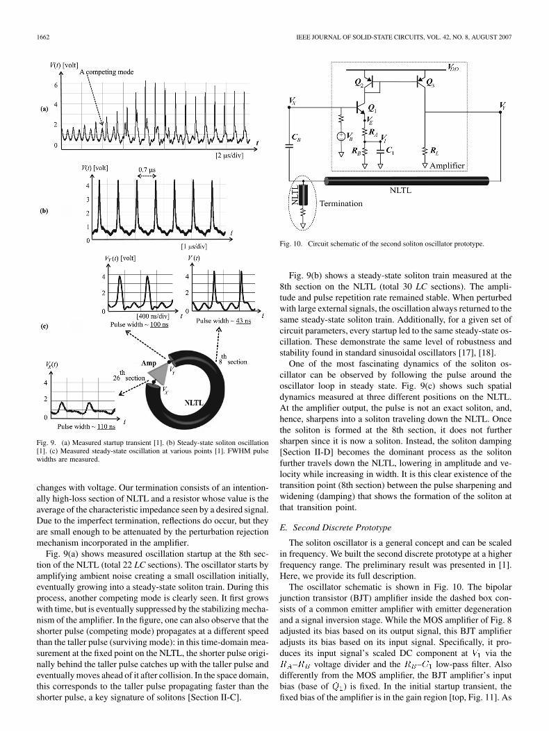
Fig. 9. (a) Measured startup transient [1]. (b) Steady-state soliton oscillation[1]. (c) Measured steady-state oscillation at various points [1]. FWHM pulsewidths are measured.
changes with voltage. Our termination consists of an intention-ally high-loss section of NLTL and a resistor whose value is theaverage of the characteristic impedance seen by a desired signal.Due to the imperfect termination, reflections do occur, but theyare small enough to be attenuated by the perturbation rejectionmechanism incorporated in the amplifier.
Fig. 9(a) shows measured oscillation startup at the 8th sec-tion of the NLTL (total 22 LC sections). The oscillator starts byamplifying ambient noise creating a small oscillation initially,eventually growing into a steady-state soliton train. During thisprocess, another competing mode is clearly seen. It first growswith time, but is eventually suppressed by the stabilizing mecha-nism of the amplifier. In the figure, one can also observe that theshorter pulse (competing mode) propagates at a different speedthan the taller pulse (surviving mode): in this time-domain mea-surement at the fixed point on the NLTL, the shorter pulse origi-nally behind the taller pulse catches up with the taller pulse andeventually moves ahead of it after collision. In the space domain,this corresponds to the taller pulse propagating faster than theshorter pulse, a key signature of solitons [Section II-C].
Fig. 10. Circuit schematic of the second soliton oscillator prototype.
Fig. 9(b) shows a steady-state soliton train measured at the8th section on the NLTL (total 30 LC sections). The ampli-tude and pulse repetition rate remained stable. When perturbedwith large external signals, the oscillation always returned to thesame steady-state soliton train. Additionally, for a given set ofcircuit parameters, every startup led to the same steady-state os-cillation. These demonstrate the same level of robustness andstability found in standard sinusoidal oscillators [17], [18].
One of the most fascinating dynamics of the soliton os-cillator can be observed by following the pulse around theoscillator loop in steady state. Fig. 9(c) shows such spatialdynamics measured at three different positions on the NLTL.At the amplifier output, the pulse is not an exact soliton, and,hence, sharpens into a soliton traveling down the NLTL. Oncethe soliton is formed at the 8th section, it does not furthersharpen since it is now a soliton. Instead, the soliton damping[Section II-D] becomes the dominant process as the solitonfurther travels down the NLTL, lowering in amplitude and ve-locity while increasing in width. It is this clear existence of thetransition point (8th section) between the pulse sharpening andwidening (damping) that shows the formation of the soliton atthat transition point.
E. Second Discrete Prototype
The soliton oscillator is a general concept and can be scaledin frequency. We built the second discrete prototype at a higherfrequency range. The preliminary result was presented in [1].Here, we provide its full description.
The oscillator schematic is shown in Fig. 10. The bipolarjunction transistor (BJT) amplifier inside the dashed box con-sists of a common emitter amplifier with emitter degenerationand a signal inversion stage. While the MOS amplifier of Fig. 8adjusted its bias based on its output signal, this BJT amplifieradjusts its bias based on its input signal. Specifically, it pro-duces its input signal’s scaled DC component at via the
– voltage divider and the – low-pass filter. Alsodifferently from the MOS amplifier, the BJT amplifier’s inputbias (base of ) is fixed. In the initial startup transient, thefixed bias of the amplifier is in the gain region [top, Fig. 11]. As

RICKETTS et al.: ON THE SELF-GENERATION OF ELECTRICAL SOLITON PULSES 1663
Fig. 11. Effective adaptive bias control in Fig. 10.
the oscillation grows and forms into a pulse train, increases,which moves the amplifier transfer curve towards right [bottom,Fig. 11], placing the fixed bias in the attenuation region. As a re-sult, in steady state, the input pulse is placed across the gain-at-tenuation regions. Summarizing, while this amplifier moves thetransfer curve instead of the amplifier bias, in steady state, itplaces the pulse train just like in Fig. 7(c), hence achieving allof the three stability mechanisms. The measured steady-statesoliton oscillation from the second prototype is shown in Fig. 12.The periodic soliton train clearly seen remained as stable as thefirst prototype.
With the soliton oscillator concept review complete in thissection, we will now move on to new contributions.
IV. FURTHER EXPERIMENTAL STUDIES ON THE SOLITON
OSCILLATOR DYNAMICS
A. Existence of a Limit Cycle
In [1], the stability of the soliton oscillator was demonstratedby steady-state oscillations that were robust to ambient and ex-ternal perturbations. The key character of any stable oscillatoris the existence of a limit cycle in phase space. For instance,for an LC oscillator whose voltage across the LC tank is , the
Fig. 12. Soliton oscillation from the second prototype [1].
Fig. 13. (a) Steady-state trajectory of (V; dV=dt). (b) Transient response to asignificant disturbance. (c) Steady-state trajectory after the effect of perturbationhas settled.
steady-state oscillation maps onto an ellipse-like closed trajec-tory (limit cycle) in a 2-D space (phase space). Re-gardless of the initial condition or after perturbations, the os-cillation point always ends up on the limit cycle insteady state.
Here, we experimentally demonstrate the existence of a limitcycle in the soliton oscillator, using the first discrete prototype[Section III-D]. The low-frequency discrete prototype is used tofacilitate a large perturbation of the system. Fig. 13(a) shows thetrajectory of the steady-state oscillation point in the
1664 IEEE JOURNAL OF SOLID-STATE CIRCUITS, VOL. 42, NO. 8, AUGUST 2007
Fig. 14. WpA versus A.
2-D phase space where is the voltage taken from the 7th nodeon the NLTL.2 After a significant perturbation of the soliton os-cillator using an external pulsed source, the oscillation trajectoryin the phase space deviates from the steady-state trajectory ofFig. 13(a) for many cycles as depicted in Fig. 13(b), but it even-tually settles back to the same original steady-state trajectory[Fig. 13(c)]. This experiment demonstrates that the steady-statetrajectory of Fig. 13(a) is the limit cycle of the soliton oscillator.
B. Spatial Dynamics Revisited
The spatial dynamics of the first prototype shown in Fig. 9(c)exhibited a clear transition from pulse sharpening to pulsewidening. There we reasoned that the sharpening and wideningcorrespond to soliton-forming and soliton-damping processes,respectively.
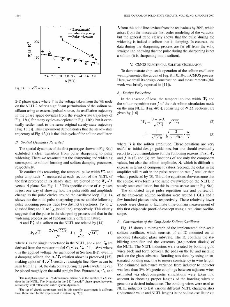
To confirm this reasoning, the temporal pulse width andpulse amplitude , measured at each section of the NLTL ofthe first prototype in its steady state, are plotted in theversus plane. See Fig. 14.3 This specific choice of – axesis just one way of showing how the pulsewidth and amplitudechange as the pulse circles around the oscillator loop. Fig. 14shows that the initial pulse sharpening process and the followingpulse widening process trace two distinct trajectories, to(dashed line) and to (solid line), respectively. This clearlysuggests that the pulse in the sharpening process and that in thewidening process are of fundamentally different nature.
and of a soliton on the NLTL are related by [14]
(1)
where is the single inductance in the NLTL, and and arederived from the varactor model where
is the applied voltage. As mentioned in Section II-D, even ina damping soliton, the – relation above is preserved [15],making a plot of versus a straight line. Now as can beseen from Fig. 14, the data points during the pulse widening canbe placed roughly on the solid straight line. Extracted , , and
2The real phase space is 2N -dimensional whereN is the number of LC sec-tions in the NLTL. The dynamics in the 2-D “pseudo”-phase-space, however,reasonably well reflects the entire system dynamics.
3The set of circuit parameters used in this specific experiment is differentfrom those used for the experiment to obtain Fig. 9(c).
from this solid line deviate from the real values by 20%, whicharises from the inaccurate first-order modeling of the varactor,but the general trend clearly shows that the pulse during thewidening is indeed a soliton that is damping. In contrast, thedata during the sharpening process are far off from the solidstraight line, showing that the pulse during the sharpening is nota soliton (it is sharpening into a soliton).
V. CMOS ELECTRICAL SOLITON OSCILLATOR
To demonstrate chip-scale operation of the soliton oscillator,we implemented the circuit of Fig. 8 in 0.18- m CMOS process.Here, we detail its design, construction, and measurements (thiswork was briefly reported in [11]).
A. Design Procedure
In the absence of loss, the temporal soliton width andthe soliton repetition rate of the th soliton circulation modeon the ring NLTL [Fig. 4(b)], consisting of LC sections, aregiven by [16]
(2)
(3)
where is the soliton amplitude. These equations are veryuseful as initial design guidelines, but one should eventuallyresort to circuit simulations for the following reasons. First,and in (2) and (3) are functions of not only the componentvalues, but also the soliton amplitude, , which is difficult toexpress in terms of component values. Second, the delay in theamplifier will result in the pulse repetition rate smaller thanwhat is predicted by (3). Third, the equations above assume thatthe soliton waveform is the same everywhere on the NLTL insteady-state oscillation, but this is untrue as we saw in Fig. 9(c).
The simulated target pulse repetition rate and pulsewidthof the chip-scale soliton oscillator were around 1 GHz and afew hundred picoseconds, respectively. These relatively lowerspeeds were chosen to facilitate time-domain measurement ofthis first chip-scale proof-of-concept using a real-time oscillo-scope.
B. Construction of the Chip-Scale Soliton Oscillator
Fig. 15 shows a micrograph of the implemented chip-scalesoliton oscillator, which consists of an IC mounted on anin-house fabricated glass substrate. The IC contains the sta-bilizing amplifier and the varactors ( -junction diodes) ofthe NLTL. The NLTL inductors were created by bonding goldwires back and forth between the pads on the IC and metallicpads on the glass substrate. Bonding was done by using an au-tomated bonding machine to ensure consistency in wire length.The estimated inductance variation from inductor to inductorwas less than 5%. Magnetic couplings between adjacent wiresestimated via electromagnetic simulations were taken intoaccount in choosing proper lengths of the bonding wires togenerate a desired inductance. The bonding wires were used asNLTL inductors to test various different NLTL characteristics(inductance value and NLTL length) in the soliton oscillator via
RICKETTS et al.: ON THE SELF-GENERATION OF ELECTRICAL SOLITON PULSES 1665
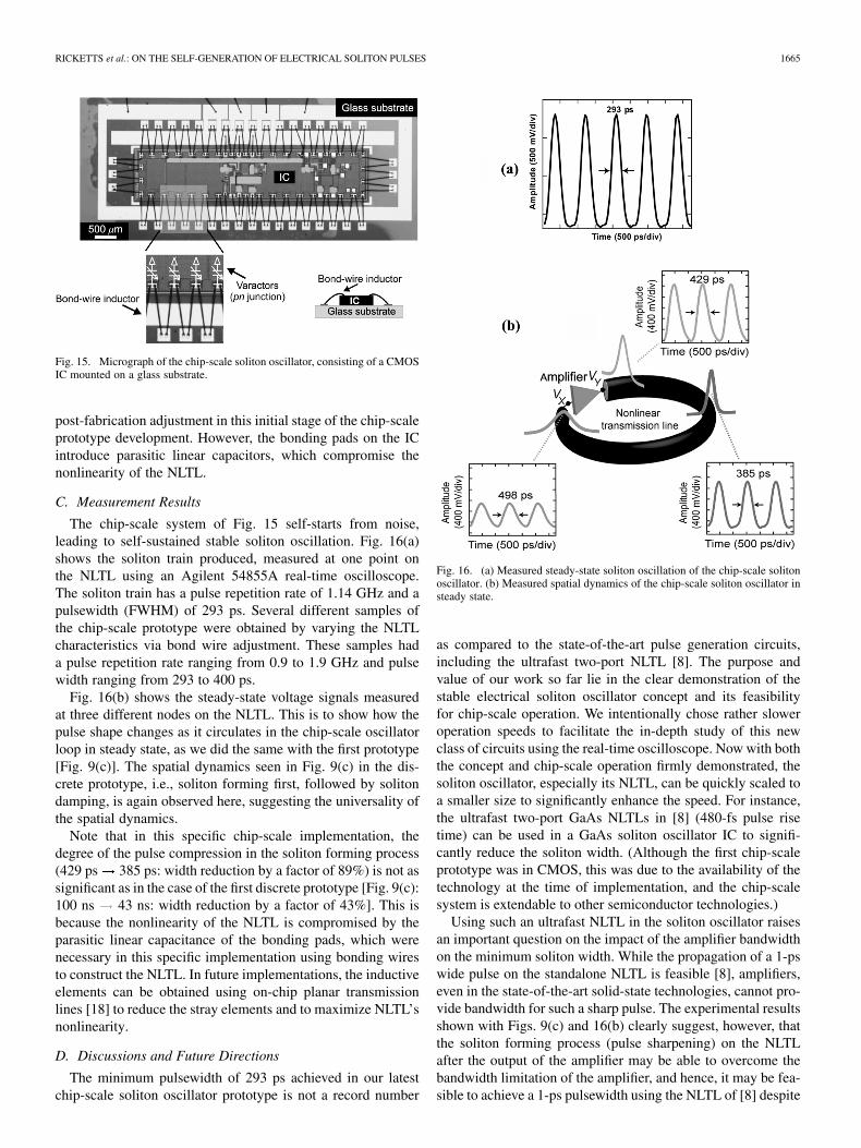
Fig. 15. Micrograph of the chip-scale soliton oscillator, consisting of a CMOSIC mounted on a glass substrate.
post-fabrication adjustment in this initial stage of the chip-scaleprototype development. However, the bonding pads on the ICintroduce parasitic linear capacitors, which compromise thenonlinearity of the NLTL.
C. Measurement Results
The chip-scale system of Fig. 15 self-starts from noise,leading to self-sustained stable soliton oscillation. Fig. 16(a)shows the soliton train produced, measured at one point onthe NLTL using an Agilent 54855A real-time oscilloscope.The soliton train has a pulse repetition rate of 1.14 GHz and apulsewidth (FWHM) of 293 ps. Several different samples ofthe chip-scale prototype were obtained by varying the NLTLcharacteristics via bond wire adjustment. These samples hada pulse repetition rate ranging from 0.9 to 1.9 GHz and pulsewidth ranging from 293 to 400 ps.
Fig. 16(b) shows the steady-state voltage signals measuredat three different nodes on the NLTL. This is to show how thepulse shape changes as it circulates in the chip-scale oscillatorloop in steady state, as we did the same with the first prototype[Fig. 9(c)]. The spatial dynamics seen in Fig. 9(c) in the dis-crete prototype, i.e., soliton forming first, followed by solitondamping, is again observed here, suggesting the universality ofthe spatial dynamics.
Note that in this specific chip-scale implementation, thedegree of the pulse compression in the soliton forming process(429 ps 385 ps: width reduction by a factor of 89%) is not assignificant as in the case of the first discrete prototype [Fig. 9(c):100 ns 43 ns: width reduction by a factor of 43%]. This isbecause the nonlinearity of the NLTL is compromised by theparasitic linear capacitance of the bonding pads, which werenecessary in this specific implementation using bonding wiresto construct the NLTL. In future implementations, the inductiveelements can be obtained using on-chip planar transmissionlines [18] to reduce the stray elements and to maximize NLTL’snonlinearity.
D. Discussions and Future Directions
The minimum pulsewidth of 293 ps achieved in our latestchip-scale soliton oscillator prototype is not a record number
Fig. 16. (a) Measured steady-state soliton oscillation of the chip-scale solitonoscillator. (b) Measured spatial dynamics of the chip-scale soliton oscillator insteady state.
as compared to the state-of-the-art pulse generation circuits,including the ultrafast two-port NLTL [8]. The purpose andvalue of our work so far lie in the clear demonstration of thestable electrical soliton oscillator concept and its feasibilityfor chip-scale operation. We intentionally chose rather sloweroperation speeds to facilitate the in-depth study of this newclass of circuits using the real-time oscilloscope. Now with boththe concept and chip-scale operation firmly demonstrated, thesoliton oscillator, especially its NLTL, can be quickly scaled toa smaller size to significantly enhance the speed. For instance,the ultrafast two-port GaAs NLTLs in [8] (480-fs pulse risetime) can be used in a GaAs soliton oscillator IC to signifi-cantly reduce the soliton width. (Although the first chip-scaleprototype was in CMOS, this was due to the availability of thetechnology at the time of implementation, and the chip-scalesystem is extendable to other semiconductor technologies.)
Using such an ultrafast NLTL in the soliton oscillator raisesan important question on the impact of the amplifier bandwidthon the minimum soliton width. While the propagation of a 1-pswide pulse on the standalone NLTL is feasible [8], amplifiers,even in the state-of-the-art solid-state technologies, cannot pro-vide bandwidth for such a sharp pulse. The experimental resultsshown with Figs. 9(c) and 16(b) clearly suggest, however, thatthe soliton forming process (pulse sharpening) on the NLTLafter the output of the amplifier may be able to overcome thebandwidth limitation of the amplifier, and hence, it may be fea-sible to achieve a 1-ps pulsewidth using the NLTL of [8] despite

1666 IEEE JOURNAL OF SOLID-STATE CIRCUITS, VOL. 42, NO. 8, AUGUST 2007
Fig. 17. Chaotic soliton oscillator.
the relatively slower amplifier. The explicit demonstration ofthis interesting possibility remains an open question, and wouldbe a natural extension of this work.
Final remark: the soliton oscillator of Fig. 4(a) used so farto prove stable soliton oscillation uses a lumped amplifier. Thedesign of a distributed soliton oscillator where gain is providedall along the NLTL could be an important direction in the furtherdevelopment of the oscillator.
VI. CHAOTIC SOLITON OSCILLATOR
We have so far focused on stable soliton oscillation by devel-oping the amplifier that can control the unruly soliton behaviors.Now let us look at the opposite end of the spectrum, and con-sider if one can attain an extreme oscillation instability, or chaos,by promoting the unruly soliton dynamics. The discussion inSection III-B suggests that one way of promoting the soliton’sunruly behavior is to increase the signal saturation in the am-plifier in the soliton oscillator of Fig. 4(a). This could intensifyoscillation instabilities (variations in pulse amplitude and repe-tition rate) through increased soliton collision events, possiblyleading to chaotic oscillations, as the authors suggested in [23].
To examine the possibility of chaotic oscillation, we considerthe circuit of Fig. 17. This is of the same topology as the originalsoliton oscillator of Fig. 4(a) in that an amplifier and an NLTLare combined in a ring. But since neither preservation of pulsepolarity nor stability mechanism is required in the amplifier toattain chaos, we opted for an inverting amplifier consisting ofthree CMOS inverter stages for simplicity. The inverting ampli-fier also facilitates signal saturation and obviates the need for aDC-blocking capacitor like in Figs. 8 and 10.
Using Cadence, we performed transistor-level transient simu-lations for the circuit (24 LC sections for the NLTL; nHwith a 1.3 series resistance. The complex varactor model usedin the simulation, if Taylor-expanded, gives
with pF and ). Fig. 18(a) shows simu-lated voltage at one node on the NLTL, while Fig. 18(b)shows its Fourier transform. The unstable oscillation in time do-main and the broad spectral distribution hint at chaotic oscilla-tion. Figs. 18(c) and (d) show the oscillation trajectories in the
phase space for two different time spans: as the timespan increases [Fig. 18(d)], the trajectory fills more of what ap-pears to be a bounded region. This phase space dynamics onceagain indicates that the oscillation may be chaotic.
Fig. 18. Simulation of the circuit of Fig. 17. (a) Time-domain signal, V (t), atone node on the NLTL. (b) Fourier transform of V (t). (c) Phase space dynamicsfrom t = 49:5 �s to t = 50 �s. (d) Phase space dynamics from t = 47:5 �sto t = 50 �s.
The hallmark property of a chaotic system is that the dis-tance of two phase-space points initially proximate to eachother (very close initial condition: ) will grow expo-nentially with time. We simulated a model mimicking the cir-cuit of Fig. 17 in Matlab and Fig. 19 shows the evolution of
where . It increases linearly withtime (positive slope), confirming that exponentially growsand the oscillator is indeed chaotic. (The slope is the Lyapunovexponent, whose positiveness is a sufficient indicator of chaosin general [24].)
Electrical chaos generators are of significant engineering in-terest due to their potential use in applications such as encryptedchaotic communications [25]. While chaos generation circuits

RICKETTS et al.: ON THE SELF-GENERATION OF ELECTRICAL SOLITON PULSES 1667
Fig. 19. Simulated log(d(t)=d(0)) versus t.
abound, the chaotic soliton oscillator may have an edge withits potentially very large bandwidth owed to the NLTL’s solitoncompression capability [6]–[8].
VII. CONCLUSION
While the hegemony of sinusoidal signals for high-frequencysignal processing in electronics will undoubtedly last into theforeseeable future, certain non-sinusoidal signals, such as short-duration pulses and chaotic signals, may further enrich the scopeand capacity of modern electronics. The electrical soliton oscil-lator presented in this paper can self-generate both a stable trainof short soliton pulses and a chaotic signal, by taming or encour-aging the unruly nature of solitons. The soliton’s superb abilityof pulsewidth compression and resultant large bandwidth maygive the edge to the electrical soliton oscillator over other pulseand chaos generation circuits. This prospect is brightened bythe notion that nature’s most intricate and brilliant circuit, thehuman brain, utilizes soliton-like neuron impulses, and often,their chaotic behaviors.
ACKNOWLEDGMENT
The authors thank M. DePetro, W. Andress, A. Belabbas, andProf. R. Brockett of Harvard University for discussions, andL. DeVito and R. Sullivan of Analog Devices for help with thebonding-wire NLTL construction. Prof. T. H. Lee of StanfordUniversity shared invaluable insights for the chaotic soliton os-cillator work. The authors also thank Prof. C. Sodini and K. Ryuof MIT for their help with varactor characterizations.
REFERENCES
[1] D. S. Ricketts, X. Li, and D. Ham, “Electrical soliton oscillator,” IEEETrans. Microw. Theory Tech., vol. 54, no. 1, pp. 373–382, Jan. 2006.
[2] M. Kahrs, “50 years of RF and microwave sampling,” IEEE Trans.Microw. Theory Tech., vol. 51, no. 6, pp. 1787–1805, Jun. 2003.
[3] R. Y. Yu, M. Reddy, J. Pusl, S. T. Allen, M. Case, and M. J. W.Rodwell, “Millimeter-wave on-wafer waveform and network mea-surements using active probes,” IEEE Trans. Microw. Theory Tech.,vol. 43, no. 4, pp. 721–729, Apr. 1995.
[4] R. Y. Yu, J. Puls, K. Yoshiyuki, M. Case, K. Masayuki, and M. Rod-well, “A time-domain millimeter-wave vector network analyzer,” IEEEMicrow. Guided Wave Lett., vol. 2, no. 8, pp. 319–321, Aug. 1992.
[5] G. F. Ross, “Transmission and reception system for generating and re-ceiving base-band pulse duration pulse signals without distortion forshort base-band communication system,” U.S. Patent 3,728,632, Apr.17, 1973.
[6] M. J. Rodwell, S. T. Allen, R. Y. Yu, M. G. Case, U. Bhattacharya, M.Reddy, E. Carman, M. Kamegawa, Y. Konishi, J. Pusl, and R. Pullela,“Active and nonlinear wave propagation devices in ultrafast electronicsand optoelectronics,” Proc. IEEE, vol. 82, no. 7, pp. 1037–1059, Jul.1994.
[7] J. R. Alday, “Narrow pulse generation by nonlinear transmission lines,”Proc. IEEE, vol. 22, no. 6, p. 739, Jun. 1964.
[8] D. W. van der Weide, “Delta-doped Schottky diode nonlinear transmis-sion lines for 480-fs, 3.5-V transients,” Appl. Phy. Lett., vol. 65, no. 7,pp. 881–883, Aug. 1994.
[9] C. J. Chen, P. K. A. Wai, and C. R. Menyuk, “Soliton fiber ring laser,”Opt. Lett., vol. 17, no. 6, pp. 417–419, Mar. 1992.
[10] W. Andress, D. S. Ricketts, X. Li, and D. Ham, “Passive and active con-trol of regenerative standing and soliton waves,” in Proc. IEEE CustomIntegrated Circuits Conf. (CICC), 2006, pp. 29–36.
[11] D. S. Ricketts and D. Ham, “A chip-scale electrical soliton mode-locked oscillator,” in IEEE Int. Solid-State Circuits Conf. (ISSCC) Dig.Tech. Papers, 2006, pp. 432–433.
[12] A. C. Scott, F. Y. F. Chu, and D. W. McLaughlin, “The soliton: Anew concept in applied science,” Proc. IEEE, vol. 61, no. 10, pp.1443–1483, Oct. 1973.
[13] P. G. Drazin and R. S. Johnson, Solitons: An Introduction. Cam-bridge, U.K.: Cambridge Univ. Press, 1989.
[14] M. Remoissenet, Waves Called Solitons: Concepts and Experiments.New York: Springer, 1999.
[15] E. Ott and R. N. Sudan, “Damping of solitary waves,” The Physics ofFluids, vol. 13, no. 6, pp. 1432–1434, Jun. 1970.
[16] D. Ricketts, “The electrical soliton oscillator,” Ph.D. dissertation, Har-vard Univ., Cambridge, MA, 2006.
[17] D. Ham and A. Hajimiri, “Concepts and methods in optimization ofintegrated LC VCOs,” IEEE J. Solid-State Circuits, vol. 36, no. 6, pp.896–909, Jun. 2001.
[18] W. Andress and D. Ham, “Standing wave oscillators utilizing wave-adaptive tapered transmission lines,” IEEE J. Solid-State Circuits, vol.40, no. 3, pp. 638–651, Mar. 2005.
[19] G. J. Ballantyne, P. T. Gough, and D. P. Taylor, “Periodic solutions ofToda lattice in loop nonlinear transmission line,” Electron. Lett., vol.29, no. 7, pp. 607–609, Apr. 1993.
[20] G. J. Ballantyne, “Periodically amplified soliton systems,” Ph.D. dis-sertation, Univ. of Canterbury, Christchurch, New Zealand, 1994.
[21] H. A. Haus, “Mode-locking of lasers,” IEEE J. Sel. Topics QuantumElectron., vol. 6, no. 6, pp. 1173–1185, Nov./Dec. 2000.
[22] C. C. Cutler, “The regenerative pulse generator,” Proc. Inst. Radio Eng.,vol. 43, no. 2, pp. 140–148, Feb. 1955.
[23] D. Ham, X. Li, S. A. Denenberg, T. H. Lee, and D. S. Ricketts, “Or-dered and chaotic electrical solitons: communication perspectives,”IEEE Commun. Mag., vol. 44, no. 12, pp. 126–135, Dec. 2006.
[24] E. Ott, Chaos in Dynamical Systems. Cambridge, U.K.: CambridgeUniv. Press, 1993.
[25] K. Cuomo and A. Oppenheim, “Synchronization of Lorenz-basedchaotic circuits with applications to communications,” IEEE Trans.Circuits Syst. II, Analog Digit. Signal Process., vol. 40, no. 10, pp.626–633, Oct. 1993.
David S. Ricketts (S’98–M’06) received the B.S.and M.S. degrees in electrical engineering fromWorcester Polytechnic Institute, Worchester, MA,and the Ph.D. degree in electrical engineering fromHarvard University, Cambridge, MA.
He is an Assistant Professor of Electrical andComputer Engineering at Carnegie Mellon Univer-sity, Pittsburgh, PA. He worked in industry from1995 to 2003 developing a wide array of analogand mixed-signal integrated circuits in BJT andsubmicron CMOS technologies. From 2003 to 2006,
he was a research assistant at Harvard University developing soliton-basedcircuits and nanowire flexible electronics. His current research interests includeultra-fast RF integrated circuits and devices, soliton electronics, nanoscaleelectronics, and quantum devices.
Dr. Ricketts was awarded the Analog Devices Fellowship at Worcester Poly-technic Institute, was a 2004 Innovation Fellow at Harvard University, and wasawarded the Analog Devices Outstanding Student Designer Award in 2006.
1668 IEEE JOURNAL OF SOLID-STATE CIRCUITS, VOL. 42, NO. 8, AUGUST 2007
Xiaofeng Li (S’05) attended Tsinghua University,Beijing, China for undergraduate study in 1998.After two years, he transferred to California Insti-tute of Technology (Caltech), Pasadena, where hereceived the B.S. degree in electrical engineeringin 2004. He is currently working toward the Ph.D.degree in electrical engineering and applied physicsat Harvard University, Cambridge, MA.
His main research interest lies in the design andexperimentation of gigahertz-to-terahertz ultrafastquantum circuits using low-dimensional nanoscale
devices, such as quantum dots, nanowires, and carbon nanotubes.Mr. Li was the recipient of a Gold Medal at the 29th International Physics
Olympiad, Reykjavik, Iceland, 1998. He ranked first in the Boston Area Un-dergraduate Physics Competition (U.S. intercollegiate physics competition) inboth 2001 and 2002. He was also the recipient of the 2002 California Institute ofTechnology Henry Ford II Scholar Award, the 2004 Harvard University PierceFellowship, and the 2005 Analog Devices Outstanding Student Designer Award.
Nan Sun (S’06) received the B.S. degree inelectrical engineering from Tsinghua University,Beijing, China, in 2006. He is currently workingtoward the Ph.D. degree in electrical engineeringat Harvard University, Cambridge, MA, wherehis major research interests lie in RF, analog andmixed-signal integrated circuit design, and also insilicon bio-molecular sensors.
He ranked first in the Department of Microelec-tronics at Tsinghua University in graduation. He wasthe recipient of the Samsung Outstanding Student
Award in 2003, Hewlett Packard Outstanding Student Award in 2006, andAnalog Device Outstanding Student Designer Award in 2007.
Kyoungho Woo (S’03) received the B.S. degree fromSeoul National University, Seoul, Korea, in 1999, andthe M.S. degree from Stanford University, Stanford,CA, in 2004, all in electrical engineering. He is cur-rently working toward the Ph.D. degree in electricalengineering at Harvard University, Cambridge, MA,where his research focus is on PLL frequency synthe-sizers and high-speed serial links.
In 2003, he was with the Sun Microsystems, Sun-nyvale, CA, where he developed a timing analysiscode for the Ultrasparc III microprocessor. He is cur-
rently working as a part-time employee at Cavium Networks, Marlborough,MA, where he is developing a multi-standard high-speed serial links transmitter.
Mr. Woo is a Fellow of the Korea Foundation for Advanced Studies, and is therecipient of the Analog Devices Outstanding Student Designer Award in 2006.
Donhee Ham (S’99–M’02) received the B.S. degreein physics in 1996 from Seoul National University,Korea, graduating with Presidential Honor atop theNatural Science College, and the Ph.D. degree inelectrical engineering from the California Institute ofTechnology (Caltech), Pasadena, in 2002, winningthe Charles Wilts Doctoral Thesis Prize (best thesisaward in electrical engineering).
Dr. Ham is currently an Associate Professor inelectrical engineering and applied physics withthe School of Engineering and Applied Sciences,
Harvard University, Cambridge, MA. His work experience also includes theCaltech-MIT Laser Interferometer Gravitational Wave Observatory (LIGO),1997/1998, IBM T. J. Watson Research Center, 2000, IEEE conferencetechnical program committees including International Solid-State CircuitsConference (ISSCC), and industry/government technical advisory positions onsubjects including ultrafast solid-state electronics and science and technologyat the nanoscale. He is a co-editor of CMOS Biotechnology (Springer, 2007).The current research focus of his research group at Harvard is on: RF, mi-crowave, analog and mixed-signal ICs; gigahertz-to-terahertz ultrafast quantumcircuits using low-dimensional nanoscale devices; soliton and nonlinear waveelectronics; and applications of CMOS ICs in biotechnology.
Dr. Ham was the recipient of the Caltech Li Ming Scholarship and IBM Grad-uate Research Fellowship. He was also the recipient of the 2003 IBM FacultyPartnership Award. He shared Harvard’s Hoopes prize (best senior thesis award)in 2003 with Mr. William Andress.