ieee transactions on circuits and systems—i:...
TRANSCRIPT

IEEE TRANSACTIONS ON CIRCUITS AND SYSTEMS—I: REGULAR PAPERS, VOL. 56, NO. 11, NOVEMBER 2009 2411
Design and Implementation of Cost-EffectiveProbabilistic-Based Noise-Tolerant VLSI Circuits
I-Chyn Wey, Student Member, IEEE, You-Gang Chen, Student Member, IEEE, Chang-Hong Yu,An-Yeu AndyWu, Member, IEEE, and Jie Chen, Senior Member, IEEE
Abstract—As the size of CMOS devices is scaled down tonanometers, noise can significantly affect circuit performance.Because noise is random and dynamic in nature, a proba-bilistic-based approach is better suited to handle these typesof errors compared with conventional CMOS designs. In thispaper, we propose a cost-effective probabilistic-based noise-tol-erant circuit-design methodology. Our cost-effective method isbased on master-and-slave Markov random field (MRF) mappingand master-and-slave MRF logic-gate construction. The resultingprobabilistic-based MRF circuit trades hardware cost for circuitreliability. To demonstrate a noise-tolerant performance, an 8-bitMRF carry-lookahead adder (MRF_CLA) was implemented usingthe 0.13- m CMOS process technology. The chip measurementresults show that the proposed master-and-slave MRF_CLA canprovide a � �� ��
� bit-error rate (BER) under 10.6-dBsignal-to-noise ratio, while the conventional CMOS_CLA can onlyprovide � �� ��
� BER. Because of high noise immunity, themaster-and-slave MRF_CLA can operate under 0.25 V to toleratenoise interference with only 1.9 W/MHz of energy consumption.Moreover, the transistor count can be reduced by 42% as com-pared with the direct-mapping MRF_CLA design [1].
Index Terms—Cost-effective hardware design, Markov randomfield (MRF), master-and-slave MRF mapping, noise-tolerant cir-cuit, probabilistically based circuit.
I. INTRODUCTION
W ITH THE progress of VLSI process technology, powerconsumption and power density increase as design
complexity and transistor density in systems-on-chip (SoCs)increase. Therefore, low-power design becomes a major de-sign challenge. In general, lowering the supply voltage is themost efficient way to save power since power consumption isproportional to the square of supply voltage. Future electronicdevices are expected to operate at much a lower supply voltage
Manuscript received June 28, 2008; revised October 24, 2008. First pub-lished February 18, 2009; current version published November 04, 2009. Thiswork was supported in part by the National Science Council under Grant NSC94-2215-E-002-037, by the National Institute of Nanotechnology, and by theDiscovery Program of the Natural Sciences and Engineering Research Councilof Canada under Grant 245680. This paper was approved by Associate EditorV. De.
I.-C. Wey is with the Department of Electrical Engineering, Chang Gung Uni-versity, Taoyuan 333, Taiwan (e-mail: [email protected]).
Y.-G. Chen and A.-Y. Wu are with the Graduate Institute of ElectronicsEngineering, National Taiwan University, Taipei 10617, Taiwan (e-mail:[email protected]).
C.-H. Yu is with the College of Information and Communication Engineering,Zhejiang Gongshang University, Hangzhou 310018, China.
J. Chen is with the National Institute for Nanotechnology, Ottawa, ON K1A0R6, Canada, and also with the Department of Electrical and Computer Engi-neering and the Department of Biomedical Engineering, University of Alberta,Edmonton, AB T6G 2V4, Canada.
Digital Object Identifier 10.1109/TCSI.2009.2015648
than traditional designs, which is very useful for portable elec-tronics and biomedical implants. Unfortunately, when supplyvoltage decreases, noise does not decrease proportionally. Asa result, one of the major challenges in ultralow-power anddeep-submicrometer circuit design is noise fluctuation [2]–[8].Ultradeep-submicrometer VLSI circuits are expected to operateat much smaller noise margins, and thus, VLSI circuits aremore sensitive to noise.
Many low-noise or noise-tolerant circuit techniques wereproposed recently [9]–[13], but they all focus on dealing withspecific types of noise, such as crosstalk noise and substratenoise. These designs cannot effectively solve the randomintrinsic noise in ultradeep-submicrometer or future nanoscaleVLSI systems [14], [15]. The triple-majority-redundant (TMR)methods [16], [17] are popular solutions to device failure. Ifany one of the three circuits fails, the other two circuits canstill correct faults. However, intrinsic noise can significantlyinterfere with each signal, and the noisy signals often renderwrong voting results in TMR. Therefore, TMR cannot effec-tively solve the random intrinsic noise that often occurs innanoscale circuits. The error correction code (ECC) techniquesare pervasively and successfully used to correct the transmis-sion data in communication systems. However, we do not haveprior knowledge about what types of errors could occur innanoscale circuitry, and thus, it is very difficult to select the besttype of error coding scheme. Moreover, ECC achieves highererror-correction capability at the expense of higher latency.ECC techniques applied in communication systems may not bethe ideal choice to solve intrinsic noise in nanoscale circuits.The neural network structure [18] is another approach, whichprovides continuous adaptation to errors. However, trainingsequences are difficult to obtain in advance, and the neuralnetwork is also difficult to implement.
Because intrinsic noise is random and dynamic in nature,conventional deterministic logic design methods used in CMOScircuits are insufficient to handle these faults. Probabilistic ap-proaches are more desirable to handle this problem [1],[19]–[21]. In probabilistic-based noise-tolerant approaches, thenoise energy is shared and averaged by the whole system; there-fore, the noise signal level can be greatly reduced. As a result,noise tolerance can be enhanced by using probabilistic-basedapproaches.
In this paper, the probabilistic-based noise-tolerant circuitsare designed based on the Markov random field (MRF) theory[19]. The basic idea of MRF design is as follows: Under theprobabilistic framework, we cannot expect logic values (‘0’or ‘1’) in a circuit at a particular time to be correct. We canonly expect the probability distribution of the values to have
1549-8328/$26.00 © 2009 IEEE
Authorized licensed use limited to: National Taiwan University. Downloaded on March 02,2010 at 08:23:32 EST from IEEE Xplore. Restrictions apply.

2412 IEEE TRANSACTIONS ON CIRCUITS AND SYSTEMS—I: REGULAR PAPERS, VOL. 56, NO. 11, NOVEMBER 2009
the highest likelihood of being in a correct logic state. Theappropriate mathematical framework for this type of analysis isthe MRF, which was initially developed in [19] to support theoptimization of the values of a large set of random variablesso that their overall joint probability has a global maximum.A possible MRF circuit design was presented in [20] and[21], where the MRF theory was mapped onto logic circuits.An MRF silicon chip design was further presented in [1]to prove the design concept of noise-tolerant MRF circuits.As demonstrated in [1], [20], and [21], the probabilisticallybased circuits can achieve much better noise immunity thantheir CMOS counterparts. However, the hardware overhead ofMRF direct-mapping circuits in [1] is much larger than that ofdeterministically based CMOS circuits.
In this paper, a cost-effective design is proposed to providenearly the same noise-tolerant performance, but with lowerhardware overhead through MRF network simplification. Oursimplification method is based on master-and-slave MRFmapping and master-and-slave MRF logic-gate construction.To demonstrate the design methodology, we implemented an8-bit MRF carry-lookahead adder (MRF_CLA) using 0.13- mCMOS process technology. The number of transistors in theproposed cost-effective MRF_CLA can be significantly reducedby 42% as compared with the initial direct-mapping MRFdesign in [1].
The major contributions of this work are as follows.1) Design cost-effective MRF circuit by master-and-slave
MRF mapping and master-and-slave MRF logic-gateconstruction. Instead of directly implementing all validstates in the MRF graph, we separate the truth table intotwo groups according to its output logic states and thenimplement them separately. All output states in logic“1” are collected as group “1,” while logic “0” statesare collected as group “0.” The minterms in groups “1”and “0” are implemented separately in a master fashion.The feedback stage is constructed in a slave fashion todecrease hardware cost. The hardware complexity in theproposed master-and-slave design can be greatly reduced,and the hardware overhead does not increase exponentiallywhen the number of nodes in the MRF network increases.The number of transistors in the proposed cost-effectiveMRF_CLA can be significantly reduced by 42% as com-pared with the initial direct-mapping MRF design in [1].
2) Decompose the MRF network into small subnetworksfor practical implementation. At the architectural level,we propose a practical solution to divide the whole MRFnetwork into many small-scale MRF subnetworks toreduce overall hardware complexity. Within individualMRF subnetworks, we implement the noise-tolerant logiccircuit using valid minterm feedback convergence loops.All these feedback loops are constructed by neighborhoodnodes in the same MRF subnetwork to achieve high noisetolerance. At the architectural level, we can combinethese subnetworks and thus provide a practical archi-tectural mapping solution for any computing systems.The proposed practical MRF architectural mapping canachieve good tradeoffs between hardware complexity andnoise-tolerance performance.
3) Map the MRF theory to a real silicon adder circuit(with complete measurement results) as proof of designconcept. References [19]–[21] applied the MRF theory tosolve noise interference issues at the algorithmic and logiclevels, and we extend the design idea to the architecturallevel for chip implementation. To prove the design conceptin silicon and demonstrate the noise-tolerance capability,we implemented an 8-bit MRF_CLA with the 0.13- mCMOS process technology. Some portions of the chipimplementation results have been reported in our previouspaper [22]. In this paper, we give more details about ourdesign and present some new experiments to compare cir-cuit performance in terms of noise tolerance and hardwarecost. From the measurement results, the proposed cost-ef-fective MRF_CLA can provide a bit-errorrate (BER) under 10.6-dB signal-to-noise ratio (SNR),while the conventional CMOS_CLA can only provide an
BER. Because of high noise immunity, themaster-and-slave MRF_CLA can tolerate noise interfer-ence to operate under 0.25 V with only 1.9 W/MHz ofenergy consumption.
This paper is organized as follows. In Section II, we reviewthe MRF circuit design and illustrate its superiority in noisetolerance. In Section III, we propose a cost-effective MRFnoise-tolerant circuit design by using master-and-slave MRFmapping and master-and-slave MRF logic-gate construction. InSection IV, we present a practical MRF architectural mappingsolution through MRF local network mapping. In Section V,we address the proof-of-concept chip implementation and mea-surement results. Finally, we draw a conclusion in Section VI.
II. REVIEW OF PROBABILISTIC-BASED NOISE-TOLERANT
CIRCUIT DESIGN
A. Review of MRF Noise-Tolerant Design Methodology
The MRF is a probabilistic framework that has been com-monly used in many fields, including pattern recognition andcommunications [23]–[26]. The MRF theory is first applied toenhance noise tolerance in VLSI circuit design in [20]. TheMRF approach is further extended to the design of a Hammingdecoder for the protection of memory against single event up-sets in [27]. The main idea in MRF is that output results ofan MRF network are determined by their neighborhood nodesjointly [19], [28]. Through joint estimation, the noise energy isspread and shared among MRF neighbor nodes; therefore, thenoise signal level can be greatly reduced. In this way, we canjudge the correct logic states precisely and enhance the relia-bility of computing circuits. The other main reason for selectingthe Markov random network as the basis for our design is thatits operation does not depend on perfect devices or perfect inputsignals. The following is a brief review of how MRF works.
The most important feature associated with the MRF isthe Markovian property: The probability of a given variabledepends only on its neighbors. In an MRF network, variables
represent the states of logic gates in a circuit. These logicstates are uniquely determined by circuit input or output values.Arcs or edges in an MRF network represent conditional prob-abilities relating each circuit node to its neighboring nodes.
Authorized licensed use limited to: National Taiwan University. Downloaded on March 02,2010 at 08:23:32 EST from IEEE Xplore. Restrictions apply.

WEY et al.: DESIGN AND IMPLEMENTATION OF COST-EFFECTIVE PROBABILISTIC-BASED NOISE-TOLERANT VLSI CIRCUITS 2413
Fig. 1. Mapping logic circuit onto MRF graph. (a) Sample circuit and (b) itscorresponding MRF graph.
The MRF, in principal, can encode arbitrary logic. Takingan example circuit as shown in Fig. 1(a), we can explain theMRF mapping as follows. Each logic signal terminal can beviewed as a node of the MRF network. The MRF networkis constructed based on its logic combinations. The examplecircuit can be mapped onto an MRF, as shown in Fig. 1(b).In this application, the MRF is defined by a set of randomvariables . The nodes in MRF correspondto logic signal terminals and .The Markovian property corresponds to the logic interactionsbetween nodes, i.e., . The conditionalprobability of a node state in terms of its neigh-borhood can be formulated in terms of cliques. For instance,the conditional probability of can be formulatedin terms of the clique of . A clique is a set of fullyconnected nodes, and each node connects to all the remainingnodes in the clique as its neighbors.
In a logic circuit, hundreds of internal logic signal paths existfrom its inputs to its outputs. However, only one set of variablecombination is correct. The correct set corresponds to the max-imum joint probability. Noise tolerance is achieved because theMRF network is updated iteratively in terms of the state changesof individual nodes through the network. Ultimately, the net-work converges to a stable set of states, which corresponds tothe correct logic states. Successful operation only requires thatthe energy of correct states is lower than the energy of incor-rect states [19]. Next, we review the mechanism of an MRFnoise-tolerant design via a simple example.
B. Mapping MRF Graph Onto Logic Circuits
To demonstrate how to map an MRF network onto a logiccircuit, we consider a two-input NAND gate with inputsand an output in Fig. 2(a) as an example. To map the logicfunction onto an MRF network , we first listall possible states in a truth table and mark its valid states apartfrom its invalid states, as in Fig. 2(b) [20], [21].
The design goal is to ensure that the circuit stays in thecorrect states. Based on the MRF theory, the logic output statecan be influenced by its neighboring nodes, and the correctstates correspond to its valid minterms. In the NAND example,
and are fourvalid minterms ,as shown in Fig. 2(b). Fig. 3, which was taken from [20]
Fig. 2. Logic compatibility function for a two-input NAND gate. (a) Conven-tional NAND gate and (b) logic compatibility function for a NAND gate with allpossible states.
Fig. 3. Construction of noise-tolerant NAND gate via valid minterm feedbackloops [20], [21].
and [21], shows how to construct a fault-tolerant circuit viathe “valid minterm feedback loop.” All four valid mintermsare generated by AND gates, which are collectively called thevalid minterm generator in Fig. 3. To strengthen the proba-bility of input nodes staying in the correct states, the validminterms are collected in a group and connected back to thecorresponding input nodes. For example, all three minterms
and contain the logicalvariable ; thus, their outputs are feedback connected to .By following the same design rule, the other five feedbackpaths can be connected to input nodes and ,as shown in Fig. 3.
Authorized licensed use limited to: National Taiwan University. Downloaded on March 02,2010 at 08:23:32 EST from IEEE Xplore. Restrictions apply.

2414 IEEE TRANSACTIONS ON CIRCUITS AND SYSTEMS—I: REGULAR PAPERS, VOL. 56, NO. 11, NOVEMBER 2009
Fig. 4. Simulation results of the inputs and outputs of CMOS and MRF NAND
gates.
To show how an MRF NAND works, the patternis taken as an example for illustration.
The AND gate at the very top is ‘on’ and feeds a logic ‘1’ backto the input of the OR gates shown at the bottom of Fig. 3.The other AND gates are ‘off’ and feed back logic ‘0’ Thesevalid minterm values are grouped by OR gates and fed backto all input nodes. In this case, the input and output valuesare and , and the overall circuitlatches into the correct state . The other correctconfigurations, such as
and orand , all work in the
same fashion. However, the incorrect configurations, suchas , are not stable and willconverge to a correct state through valid minterm feedbackloops, such as converging to . In otherwords, the MRF can automatically recover from incorrectstates and achieve noise tolerance. However, if incorrectstates occur in a conventional CMOS NAND gate, such as
and orand , the circuit
cannot recover automatically from its incorrect states. TheNAND gate is the basic logic combinational gate in computingsystems. The other basic MRF logic gates or complicated MRFcombinational logic can also be designed in the same way.
C. Noise-Tolerant Performance of MRF Circuits
From Fig. 3, we can observe that MRF circuits requiremore transistors than their counterpart conventional CMOSdesigns. MRF implementations, however, provide significantadvantages over standard CMOS designs in terms of noisetolerance when supply voltage is significantly decreased. Fig. 4shows the simulation results by comparing an MRF NAND
with a CMOS NAND gate. The simulations were carried outin SPICE using the 70-nm CMOS library from Berkeley [29]at room temperature. The threshold values are 0.2 V fornMOS and 0.22 V for pMOS. We used the supply voltage
, in which the gate operates in the subthresholdregion . The outputs of an MRF NAND and a
Fig. 5. Output function of the example circuit is determined by its MRF nodes.
CMOS NAND gate in the presence of very noisy input signalsare shown in Fig. 4. The top two curves are the input signals
, which are generated by adding a Gaussian noise withzero mean and a variance of 3.4 mV to logic “1” (0.15 V) andto logic ‘0’ (0.0 V). Noise with 3.4-mV variance is picked toillustrate and compare the noise-tolerance capability betweenMRF and conventional CMOS design. If the noise variationis too large, the MRF circuit will also malfunction. The noisemodel that we used can be found in [30]. The noise on the inputsignal causes the standard CMOS NAND gate to switch betweencorrect and incorrect output values, as shown in the curvesecond to the bottom in Fig. 4. In other words, the deterministicCMOS design simply cannot function when the circuit operatesunder the subthreshold condition. The probabilistic-based MRFNAND gate, on the other hand, provides excellent noise immu-nity even in the subthreshold region, as shown in the curve atthe bottom of Fig. 4.
III. COST-EFFECTIVE MRF NOISE-TOLERANT
LOGIC CIRCUIT DESIGN
A. Master-and-Slave MRF Mapping
In [1], the first working silicon chip was fabricated to provethe design concept of a noise-tolerant circuit using the MRFtheory. The circuit in Fig. 1(a) can be mapped onto an MRFgraph according to its logic combination as shown in Fig. 1(b).If we implement the MRF noise-tolerant circuit following theprocedures outlined in [1], the hardware complexity grows ex-ponentially as the scale of the MRF network increases. Morespecifically, as shown in Fig. 5, the valid function of this samplecircuit is determined by the nodes from to , and thus, thehardware complexity is proportional to (or the exponentia-tion of the number of MRF nodes).
To reduce the hardware complexity, some area-efficientMRF designs have been proposed in [31] and [32]. In [31],the hardware complexity of an MRF logic gate is reducedthrough Boolean simplification and valid minterm reduction.By mapping the MRF logic gate using the simplified Booleanequation proposed in [31], the circuit area can be greatlyreduced. In particular, high fan-in circuits can be constructedwithout exponentially increasing the circuit area. In [32], sometechniques, including clique variable sharing, implied depen-dence, and supergate techniques, were proposed to reduce thetransistor count of large-scale multilevel combinational circuitsbuilt within the MRF design. The simplified technique in [31]
Authorized licensed use limited to: National Taiwan University. Downloaded on March 02,2010 at 08:23:32 EST from IEEE Xplore. Restrictions apply.

WEY et al.: DESIGN AND IMPLEMENTATION OF COST-EFFECTIVE PROBABILISTIC-BASED NOISE-TOLERANT VLSI CIRCUITS 2415
Fig. 6. Proposed cost-effective MRF mapping method. (a) Truth table is sep-arated into two groups. (b) Output is determined by the master-and-slave MRFnetwork.
is to reduce the MRF hardware complexity in each simple logicgate. Nevertheless, the technique presented in [32] is to mergethe multilevel logical gates into simplified ones, which is asystematic approach. This approach cannot always result inhardware saving because it depends heavily on detailed circuittopology.
In this paper, a more general and cost-effective MRF de-sign is proposed and implemented to further reduce the MRFhardware complexity in each simple logic gate. Our simplifica-tion method is based on master-and-slave MRF mapping andmaster-and-slave MRF logic-gate construction. Instead of di-rectly implementing all valid states in the MRF graph, the truthtable is separated into two groups according to its output logicstates and then implemented separately in the master-and-slaveMRF fashion. As shown in Fig. 6(a), the truth table of thesample circuit in Fig. 1(a) is separated into two groups. Alloutput states in logic “1” are collected as group “1,” whilelogic “0” states are collected as group “0.” Next, minterms ingroups “1” and “0” are implemented separately. These twogroups compete to determine the circuit outputs. We call this
Fig. 7. Construction of an MRF NAND gate. (a) Direct-mapping MRF NAND
architecture. (b) Proposed cost-effective MRF NAND architecture.
first-stage design a master MRF network. To let the circuit havea better chance of staying in the correct states, the outputs areconnected back to inputs in order to reinforce the correct statesin the master MRF network. The feedback stage is named theslave MRF network. The hardware complexity in the proposedmaster-and-slave design is proportional to (or two groupstimes two stages instead of in the direct-mapping MRF de-sign), as shown in Fig. 6(b). Using this design, the hardwareoverhead does not increase exponentially while the noise-tol-erance capability is preserved.
B. Master-and-Slave MRF Logic-Gate Construction
All combinatorial circuits can be derived from basic logicgates, such as NAND, NOR, and inverters. To revisit the construc-tion of an MRF circuit, we consider a simple two-input NAND
gate with inputs and an output as an example.The MRF logic gate is constructed by the valid minterm gen-erator and the feedback connecter. The hardware complexity isdetermined by its input and output numbers.
In the direct-mapping design in [1], the MRF NAND is con-structed by a valid minterm generator (with six inputs and fourminterms) and a feedback connecter (with four inputs and sixoutputs), as shown in Fig. 7(a). In the proposed design, as shownin Fig. 7(b), we separate the valid minterm generator into twogroups to fix the minterm number to two. In this way, we canprevent the exponential increase of hardware complexity in thevalid minterm generator. Moreover, no matter how complex thevalid minterm generator circuit is, the hardware complexity inthe feedback connection is fixed. Therefore, the hardware com-plexity can be greatly reduced, particularly in the case of a logicfunction with high fan-in.
Authorized licensed use limited to: National Taiwan University. Downloaded on March 02,2010 at 08:23:32 EST from IEEE Xplore. Restrictions apply.
2416 IEEE TRANSACTIONS ON CIRCUITS AND SYSTEMS—I: REGULAR PAPERS, VOL. 56, NO. 11, NOVEMBER 2009
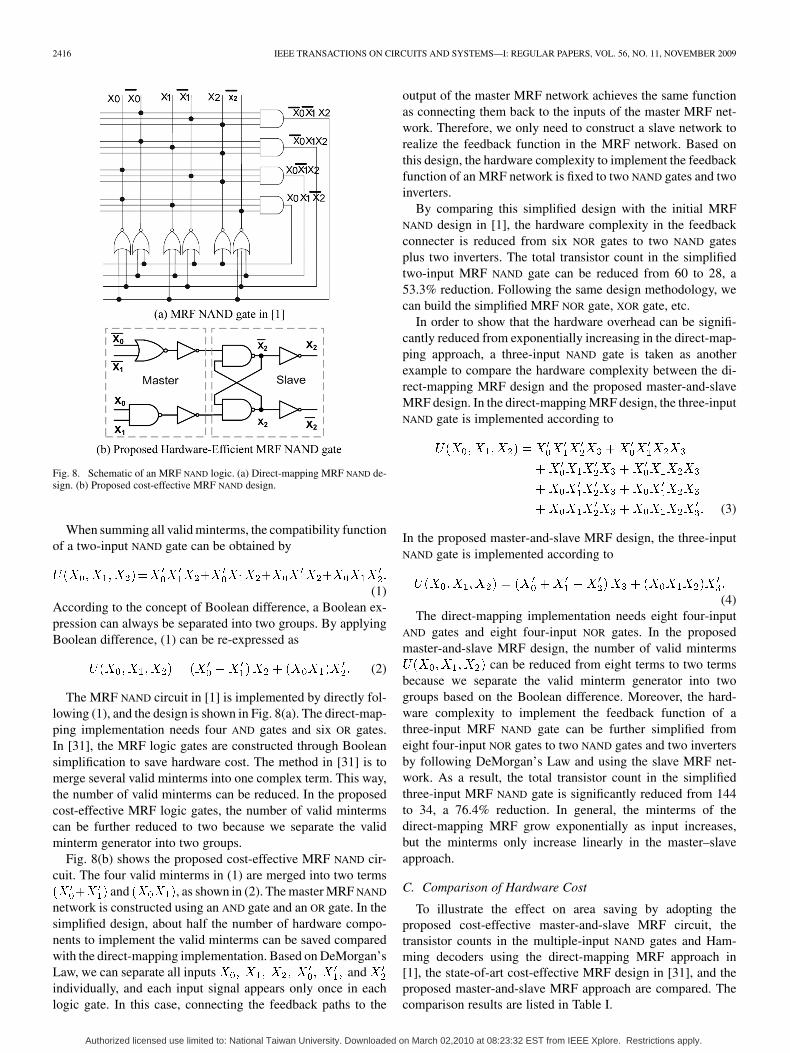
Fig. 8. Schematic of an MRF NAND logic. (a) Direct-mapping MRF NAND de-sign. (b) Proposed cost-effective MRF NAND design.
When summing all valid minterms, the compatibility functionof a two-input NAND gate can be obtained by
(1)According to the concept of Boolean difference, a Boolean ex-pression can always be separated into two groups. By applyingBoolean difference, (1) can be re-expressed as
(2)
The MRF NAND circuit in [1] is implemented by directly fol-lowing (1), and the design is shown in Fig. 8(a). The direct-map-ping implementation needs four AND gates and six OR gates.In [31], the MRF logic gates are constructed through Booleansimplification to save hardware cost. The method in [31] is tomerge several valid minterms into one complex term. This way,the number of valid minterms can be reduced. In the proposedcost-effective MRF logic gates, the number of valid mintermscan be further reduced to two because we separate the validminterm generator into two groups.
Fig. 8(b) shows the proposed cost-effective MRF NAND cir-cuit. The four valid minterms in (1) are merged into two terms
and , as shown in (2). The master MRF NAND
network is constructed using an AND gate and an OR gate. In thesimplified design, about half the number of hardware compo-nents to implement the valid minterms can be saved comparedwith the direct-mapping implementation. Based on DeMorgan’sLaw, we can separate all inputs andindividually, and each input signal appears only once in eachlogic gate. In this case, connecting the feedback paths to the
output of the master MRF network achieves the same functionas connecting them back to the inputs of the master MRF net-work. Therefore, we only need to construct a slave network torealize the feedback function in the MRF network. Based onthis design, the hardware complexity to implement the feedbackfunction of an MRF network is fixed to two NAND gates and twoinverters.
By comparing this simplified design with the initial MRFNAND design in [1], the hardware complexity in the feedbackconnecter is reduced from six NOR gates to two NAND gatesplus two inverters. The total transistor count in the simplifiedtwo-input MRF NAND gate can be reduced from 60 to 28, a53.3% reduction. Following the same design methodology, wecan build the simplified MRF NOR gate, XOR gate, etc.
In order to show that the hardware overhead can be signifi-cantly reduced from exponentially increasing in the direct-map-ping approach, a three-input NAND gate is taken as anotherexample to compare the hardware complexity between the di-rect-mapping MRF design and the proposed master-and-slaveMRF design. In the direct-mapping MRF design, the three-inputNAND gate is implemented according to
(3)
In the proposed master-and-slave MRF design, the three-inputNAND gate is implemented according to
(4)The direct-mapping implementation needs eight four-input
AND gates and eight four-input NOR gates. In the proposedmaster-and-slave MRF design, the number of valid minterms
can be reduced from eight terms to two termsbecause we separate the valid minterm generator into twogroups based on the Boolean difference. Moreover, the hard-ware complexity to implement the feedback function of athree-input MRF NAND gate can be further simplified fromeight four-input NOR gates to two NAND gates and two invertersby following DeMorgan’s Law and using the slave MRF net-work. As a result, the total transistor count in the simplifiedthree-input MRF NAND gate is significantly reduced from 144to 34, a 76.4% reduction. In general, the minterms of thedirect-mapping MRF grow exponentially as input increases,but the minterms only increase linearly in the master–slaveapproach.
C. Comparison of Hardware Cost
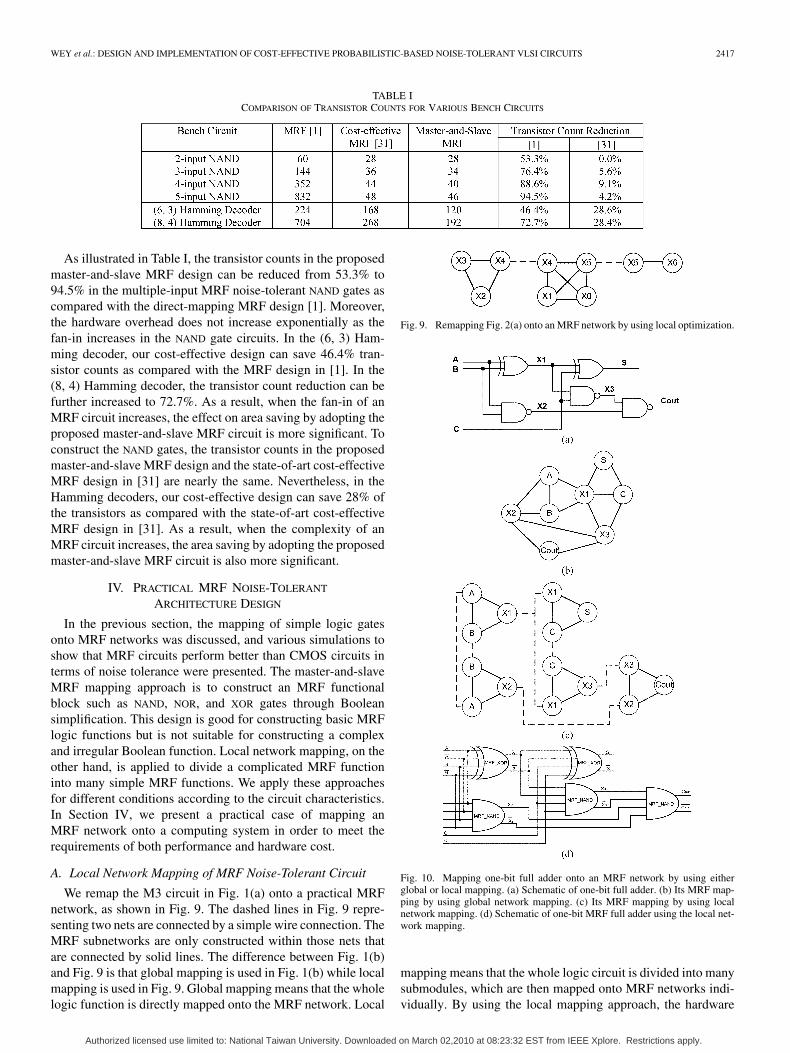
To illustrate the effect on area saving by adopting theproposed cost-effective master-and-slave MRF circuit, thetransistor counts in the multiple-input NAND gates and Ham-ming decoders using the direct-mapping MRF approach in[1], the state-of-art cost-effective MRF design in [31], and theproposed master-and-slave MRF approach are compared. Thecomparison results are listed in Table I.
Authorized licensed use limited to: National Taiwan University. Downloaded on March 02,2010 at 08:23:32 EST from IEEE Xplore. Restrictions apply.
WEY et al.: DESIGN AND IMPLEMENTATION OF COST-EFFECTIVE PROBABILISTIC-BASED NOISE-TOLERANT VLSI CIRCUITS 2417
TABLE ICOMPARISON OF TRANSISTOR COUNTS FOR VARIOUS BENCH CIRCUITS
As illustrated in Table I, the transistor counts in the proposedmaster-and-slave MRF design can be reduced from 53.3% to94.5% in the multiple-input MRF noise-tolerant NAND gates ascompared with the direct-mapping MRF design [1]. Moreover,the hardware overhead does not increase exponentially as thefan-in increases in the NAND gate circuits. In the (6, 3) Ham-ming decoder, our cost-effective design can save 46.4% tran-sistor counts as compared with the MRF design in [1]. In the(8, 4) Hamming decoder, the transistor count reduction can befurther increased to 72.7%. As a result, when the fan-in of anMRF circuit increases, the effect on area saving by adopting theproposed master-and-slave MRF circuit is more significant. Toconstruct the NAND gates, the transistor counts in the proposedmaster-and-slave MRF design and the state-of-art cost-effectiveMRF design in [31] are nearly the same. Nevertheless, in theHamming decoders, our cost-effective design can save 28% ofthe transistors as compared with the state-of-art cost-effectiveMRF design in [31]. As a result, when the complexity of anMRF circuit increases, the area saving by adopting the proposedmaster-and-slave MRF circuit is also more significant.
IV. PRACTICAL MRF NOISE-TOLERANT
ARCHITECTURE DESIGN
In the previous section, the mapping of simple logic gatesonto MRF networks was discussed, and various simulations toshow that MRF circuits perform better than CMOS circuits interms of noise tolerance were presented. The master-and-slaveMRF mapping approach is to construct an MRF functionalblock such as NAND, NOR, and XOR gates through Booleansimplification. This design is good for constructing basic MRFlogic functions but is not suitable for constructing a complexand irregular Boolean function. Local network mapping, on theother hand, is applied to divide a complicated MRF functioninto many simple MRF functions. We apply these approachesfor different conditions according to the circuit characteristics.In Section IV, we present a practical case of mapping anMRF network onto a computing system in order to meet therequirements of both performance and hardware cost.
A. Local Network Mapping of MRF Noise-Tolerant Circuit
We remap the M3 circuit in Fig. 1(a) onto a practical MRFnetwork, as shown in Fig. 9. The dashed lines in Fig. 9 repre-senting two nets are connected by a simple wire connection. TheMRF subnetworks are only constructed within those nets thatare connected by solid lines. The difference between Fig. 1(b)and Fig. 9 is that global mapping is used in Fig. 1(b) while localmapping is used in Fig. 9. Global mapping means that the wholelogic function is directly mapped onto the MRF network. Local
Fig. 9. Remapping Fig. 2(a) onto an MRF network by using local optimization.
Fig. 10. Mapping one-bit full adder onto an MRF network by using eitherglobal or local mapping. (a) Schematic of one-bit full adder. (b) Its MRF map-ping by using global network mapping. (c) Its MRF mapping by using localnetwork mapping. (d) Schematic of one-bit MRF full adder using the local net-work mapping.
mapping means that the whole logic circuit is divided into manysubmodules, which are then mapped onto MRF networks indi-vidually. By using the local mapping approach, the hardware
Authorized licensed use limited to: National Taiwan University. Downloaded on March 02,2010 at 08:23:32 EST from IEEE Xplore. Restrictions apply.

2418 IEEE TRANSACTIONS ON CIRCUITS AND SYSTEMS—I: REGULAR PAPERS, VOL. 56, NO. 11, NOVEMBER 2009
Fig. 11. (a) Example circuit to demonstrate the difference between the localand global mappings in an MRF network. (b) All possible valid states for theexample circuit using the MRF local mapping. (c) All possible valid states forthe example circuit using the MRF global mapping.
complexity to implement an MRF noise-tolerant circuit can begreatly reduced.
To demonstrate the concept of local network mapping in anMRF network, a one-bit full adder is taken as an example forillustration. The schematic of a one-bit full adder is shown inFig. 10(a). We map the one-bit full adder onto an MRF networkusing global and local mappings in Fig. 10(b) and (c), respec-tively. The circuit complexity to implement the MRF network isdetermined by the number of nodes (or the possible valid states)in an MRF network defined as . If an MRF network is imple-mented by global mapping, all possible valid states in the MRF
Fig. 12. Comparing the noise-tolerant performances of the global and localMRF mapping methods under various SNR.
Fig. 13. Architecture of a conventional 8-bit CMOS_CLA [33].
network are , which means feedback loops must beconstructed in order to construct the MRF network. Because thevalid minterm feedback loop includes the feedforward and feed-back parts, the hardware overhead in each feedback loop path istwice as large as the original CMOS design. As a result, the cir-cuit complexity to implement the MRF network is , whichis an exponential function of . If the MRF network is dividedinto many smaller MRF subnetworks, the node number in eachsubnetwork can be smaller than . The hardware complexityto implement the whole MRF network using the local mappingcan thus be greatly reduced.
As shown in Fig. 10(b), feedback loops must beconstructed to implement a one-bit MRF full adder using theglobal mapping, while only feedback loops need tobe constructed to implement a one-bit MRF full adder using thelocal mapping in Fig. 10(c). Therefore, the local mapping tech-nique is a more practical architectural mapping solution thanthe global mapping design to implement an MRF noise-tolerantcomputing system. To save hardware cost, the submodules canbe subdivided as small as possible. As shown in Fig. 10(d), a
Authorized licensed use limited to: National Taiwan University. Downloaded on March 02,2010 at 08:23:32 EST from IEEE Xplore. Restrictions apply.

WEY et al.: DESIGN AND IMPLEMENTATION OF COST-EFFECTIVE PROBABILISTIC-BASED NOISE-TOLERANT VLSI CIRCUITS 2419
Fig. 14. Mapping an 8-bit CLA onto an MRF network by using the local MRF network mapping.
one-bit MRF full adder using the local optimization only needs20 feedback loops (four feedbacks for each submodule and fivesubmodules in the adder).
B. Analysis of the Noise-Tolerant Performance and HardwareComplexity of an MRF Network
To illustrate why the noise-tolerant performance can still bepreserved when the local mapping is applied to the MRF net-work, the simple circuit in Fig. 11(a) is used. All possible validstates for the example circuit using MRF local and global net-work mappings are listed in Fig. 11(b) and (c), respectively. Intotal, there are eight valid states in the example circuit usingMRF local mapping. In the MRF global mapping case, there area total of 16 valid states, where eight states (unmarked states)are the same as in the local mapping case and the other eightstates (marked by dashed and solid rectangles) are different.The number of valid states in the global mapping case is twicethat of the local mapping case, where more redundant statescan achieve better noise immunity. However, among these eight
discrepancy states in the global mapping, there are four statesthat lead to the same output states as in the local mapping case(marked by dashed rectangle). The occurrence probability of an-other four states (marked by solid rectangles) is only 1/8 as com-pared with the eight states in the local mapping case because theinternal node has been protected by the MRF network
. Therefore, the noise tolerance in the MRF globalmapping design is improved by only 6.25%
as compared with the MRF local mapping approach.However, the hardware complexity is twice that of the MRFlocal network mapping design.
In Fig. 12, the noise-tolerant performances of global andlocal MRF mappings in the simple circuit in Fig. 11(a) arecompared. The simulations were carried out in SPICE usingthe Taiwan Semiconductor Manufacturing Company (TSMC)0.13- m CMOS process with 1.2-V supply voltage. The noisesource is additive white Gaussian noise (AWGN). By adjustingthe noise power, we can compare the BERs of the global MRFnetwork mapping and the proposed local MRF network map-ping under various SNRs. As an illustration, the global MRF
Authorized licensed use limited to: National Taiwan University. Downloaded on March 02,2010 at 08:23:32 EST from IEEE Xplore. Restrictions apply.

2420 IEEE TRANSACTIONS ON CIRCUITS AND SYSTEMS—I: REGULAR PAPERS, VOL. 56, NO. 11, NOVEMBER 2009
Fig. 15. Mapping an 8-bit CLA onto an MRF network by using the local MRF network mapping.
network mapping method can achieve a superior noise-toler-ance performance with a lower BER since all possible validstates are constructed and converged into a stable state. Thelocal network mapping technique, on the other hand, cannotachieve the same noise-tolerant ability as the global networkmapping because some possible internal valid states in theMRF network are removed. However, the degradation of thenoise-tolerant ability in local network mapping is negligible.Moreover, the design complexity and the critical path in thecomputing systems can be greatly reduced because the designcomplexity of the MRF network increases exponentially withthe number of network nodes. As a result, implementing theMRF noise-tolerant circuit with the local network mappingapproach can provide a good tradeoff between noise-tolerantperformance and design complexity and, thus, is a practicalsolution to implementing the MRF algorithm.
C. Architectural Mapping of an 8-bit MRF_CLA Circuit
In this paper, an 8-bit MRF_CLA is implemented as theproof-of-concept design to show its noise tolerance. A conven-tional 8-bit CMOS_CLA [33] is shown in Fig. 13. To realizethe 8-bit MRF_CLA through global MRF network mapping,44 nodes must be used to construct the whole MRF network.In other words, the implementation complexity of the MRFnetwork is . Such a design is impractical for real implemen-tation. On the other hand, a practical 8-bit MRF_CLA mappingarchitecture realized with local network mapping is shown inFig. 14, where the design complexity is only .
The architecture of the proposed 8-bit MRF_CLA isshown in Fig. 15. In the MRF_CLA, the MRF subnetworkis constructed within only basic logical modules, such asMRF_INV, MRF_NAND/MRF_AND, MRF_NOR/MRF _OR,and MRF_XNOR/MRF_XOR circuits. Then, the whole 8-bit
Authorized licensed use limited to: National Taiwan University. Downloaded on March 02,2010 at 08:23:32 EST from IEEE Xplore. Restrictions apply.

WEY et al.: DESIGN AND IMPLEMENTATION OF COST-EFFECTIVE PROBABILISTIC-BASED NOISE-TOLERANT VLSI CIRCUITS 2421
Fig. 16. Die photo of the MRF_CLA chip.
MRF_CLA circuit is hierarchically constructed using theseMRF submicromodules. The CLA consists of three basic logicgenerators: the PG, carry, and sum generators. In Fig. 15, thebasic logic circuits labeled “MRF” denote logic circuits that areimplemented by the MRF algorithm and represented as MRFsubnetworks of the whole 8-bit MRF_CLA. In this way, localoptimization in the output state of individual MRF submodulesis achieved. The local optimized signal can propagate stage bystage until the output states converge to a stable state.
V. CHIP IMPLEMENTATION AND MEASUREMENT RESULTS
A. Chip Implementation
To demonstrate the proof-of-concept design, a master-and-slave MRF chip, i.e., an 8-bit MRF_CLA, was fabricated usingthe TSMC 0.13- m CMOS process technology. The cost-effective MRF design was implemented using the 0.13- mCMOS technology process to show its performance under lowersupply voltage. The conventional and MRF CLA designs havealso been implemented using the 0.18- m CMOS technologyprocess to demonstrate and compare their performance in termsof noise tolerance, power, speed, and area [1]. For differentCMOS technologies, BER can be measured and comparedwith the same SNR to establish a fair baseline. The 8-bitmaster-and-slave MRF_CLA circuit was implemented basedon the MRF mapping architecture, as shown in Fig. 15. TheMRF_CLA chip die photo is shown in Fig. 16. To comparecircuit performance among the proposed master-and-slaveMRF design, the direct-mapping MRF design [1], and theconventional CMOS design, the following measurement wereperformed.
B. Measurement Results
In the previous sections, the superiority of the MRF prob-abilistic-based noise-tolerant circuits in terms of noise immu-nity was demonstrated using simulation results. However, some
Fig. 17. Measurement setup to test MRF_CLA and CMOS_CLA circuits.
restrictions and artifacts remain when the computer-aided de-sign tool was used to model noise behavior and simulate cir-cuit performance under noisy environments. Therefore, an 8-bitMRF_CLA chip was implemented to demonstrate the proof-of-concept design. By implementing the MRF design onto siliconand measuring the chip performance in real time, it cannot onlydemonstrate the superiority in the aspect of noise-immunity en-hancement but also help further clarify the noise-tolerant mech-anism in the probabilistic-based approach.
1) Measurement Setup to Test the MRF Circuit: To comparethe noise tolerance between the MRF and the CMOS design,noisy signals were injected into the inputs of an 8-bit master-and-slave MRF_CLA, an 8-bit direct-mapping MRF_CLA, andan 8-bit CMOS_CLA. These noisy signals consist of noise-freesignals generated by a pattern generator (Agilent 33250A) andnoise signals from a power supply.
The noise signals generated from the power supply areAWGN. A power splitter is used to combine the noise-freeinput signal with AWGN. The measurement setup is shown inFig. 17. Signal timing and circuit function can be verified by alogic analyzer.
2) Measurement of the MRF Circuit Single-Bit WaveformsUnder Noise Interference: Through the use of an oscilloscope(Agilent Infinium Oscilloscope DSO8104A), the waveformsof each single bit in the CLA output can be observed to com-pare its stability under noise interference. In both panels ofFig. 18(a) and (b), the upper signals are the input signals,and the lower signals are the corresponding output signals.As shown in Fig. 18, under the same noisy input signal with14.1-dB-SNR AWGN interference, the output waveform ofMRF_CLA in Fig. 18(b) is more stable than the conventionalCMOS_CLA one in Fig. 18(a). In addition to the output wave-form, the input signal of the MRF_CLA circuit is also morestable than the conventional CMOS_CLA one. The reason isthat the MRF_CLA circuit is constructed as a network in whichall nodes in the MRF network, no matter inputs or outputs, canjointly share the noise energy to make all nodes in the networkstay in a stable state. The measurement results support ourarguments that the noise energy can be jointly shared in theprobabilistic-based MRF_CLA chip and that the noise signallevel can be reduced.
3) Measure Reduplicating Signals of the MRF Circuit UnderNoise Interference: The output waveform of circuits under the
Authorized licensed use limited to: National Taiwan University. Downloaded on March 02,2010 at 08:23:32 EST from IEEE Xplore. Restrictions apply.

2422 IEEE TRANSACTIONS ON CIRCUITS AND SYSTEMS—I: REGULAR PAPERS, VOL. 56, NO. 11, NOVEMBER 2009
Fig. 18. Measured single-bit waveforms of (a) the CMOS_CLA and (b) theMRF_CLA circuits under the AWGN of 14.1-dB SNR.
Fig. 19. Reduplicating signals of (a) the CMOS_CLA and (b) the MRF_CLAcircuits under the AWGN of 14.1-dB SNR.
interference of random noise by continually reduplicating “0”and “1” signals under random noise interference is also ob-served. By comparing the reduplicating signals in Fig. 19 underthe case of AWGN interference with 14.1-dB SNR, the noisetolerance of the proposed master-and-slave MRF noise-tolerant
Fig. 20. BER comparison of both MRF_CLA and CMOS_CLA circuit undervarious SNR conditions.
circuit is shown to be much better than the CMOS_CLA cir-cuit. The noise margin or the difference between the worst “0”and “1” is 1 V in the MRF_CLA circuit under the 0.13- mprocess with 1.2-V supply voltage, while the noise margin inthe CMOS_CLA circuit is 1.2 V under the 0.18- m processwith 1.8-V supply voltage. This indicates that MRF_CLA canoperate correctly with 14.1-dB SNR AWGN interference, butthe CMOS_CLA cannot (a negative noise margin leads to com-puting error).
4) Measurement of BER Under Various SNR in the MRFCircuit: By adjusting the power levels of noise and supply,the BERs of the proposed master-and-slave MRF_CLA, thedirect-mapping MRF_CLA, and the CMOS_CLA circuitsunder various SNR conditions can be measured. In Fig. 20,the supply power is fixed, and only the noise power level isadjusted. In Fig. 20, the power supply voltage is 1.8 V for the0.18- m process and 1.2 V for the 0.13- m process, respec-tively. Based on the real-time measurement results shown inFig. 20, one can see that the noise immunity of the MRF_CLAcan be greatly enhanced compared to the CMOS_CLA. Thehigh-noise-immunity feature of the MRF circuit is very useful tolow-power silicon circuits when they operate under a very low
condition. In the 0.18- m process, the direct-mapping MRFcircuit can achieve a BER under a 10.6-dB SNRand sub-0.5-V supply-voltage condition. The direct-mappingMRF_CLA circuit consumes only 8 W/MHz under a 0.45-Vsupply. The proposed master-and-slave MRF_CLA can providea BER under a 10.6-dB SNR, while the conven-tional CMOS_CLA can only provide an BER. Themaster-and-slave MRF_CLA can operate under 0.25 V with only1.9 W/MHz of energy consumption. The simulation resultsusing the 70-nm process [29] even show that the MRF circuitcan operate with an 8-dB low SNR and 0.15-V supply voltage.
C. Chip Performance Summary
The performance comparisons of the MRF_CLA chip and theconventional CMOS_CLA chip are listed in Table II. As a com-parison, the transistor count in the conventional CMOS designis only 384, while the direct-mapping MRF design [1] needs5040 transistors and the proposed master-and-slave MRF_CLAneeds 2940 transistors. The measurement results show that the
Authorized licensed use limited to: National Taiwan University. Downloaded on March 02,2010 at 08:23:32 EST from IEEE Xplore. Restrictions apply.

WEY et al.: DESIGN AND IMPLEMENTATION OF COST-EFFECTIVE PROBABILISTIC-BASED NOISE-TOLERANT VLSI CIRCUITS 2423
TABLE IIPERFORMANCE COMPARISONS OF MRF_CLA AND CONVENTIONAL CMOS_CLA CHIPS
noise-tolerance ability of MRF design, however, is an improve-ment of times under various AWGN interference com-pared to the CMOS. Compared with the direct-mapping MRFdesign, the master-and-slave MRF design can reduce the tran-sistor count by 42% while maintaining noise immunity. Com-pared with the conventional CMOS design, the hardware com-plexity in the master-and-slave MRF design is still higher, andthe speed is slower; however, the MRF design can operate underthe subthreshold conditions to save power. The conventionalCMOS circuit, on the other hand, simply cannot operate undersuch a low-power environment. With the 0.13- m process, theproposed 8-bit MRF_CLA can achieve under 0.25 V of supplyvoltage with only 1.9 W/MHz of energy consumption. In com-parison, the conventional 8-bit CMOS_CLA chip can only op-erate correctly under 0.9 V of supply voltage.
The unavoidable worsening of noise interference in nanoscalecircuits is a problem that conventional CMOS circuit techniquescannot possibly mitigate. As a result, the proposed cost-effectiveprobabilistic-based noise-tolerant design can achieve high noiseimmunity with reasonable design overhead, which is suitable forfuture nanoscale computing systems.
VI. CONCLUSION
In this paper, we have presented the design and implemen-tation of a cost-effective probabilistically based noise-tolerantcircuit, an 8-bit MRF_CLA, using the TSMC 0.13- m CMOSprocess. The proposed master-and-slave MRF_CLA can pro-vide a BER under a 10.6-dB SNR, while theconventional CMOS_CLA can only provide anBER. The master-and-slave MRF_CLA can operate under0.25 V to tolerate noise interference with only 1.9 W/MHzof energy consumption. Moreover, the transistor count can bereduced by 42% as compared to the direct-mapping MRF_CLAdesign [1].
ACKNOWLEDGMENT
The authors would like to thank the National Chip Implemen-tation Center, Taiwan, for the chip implementation support.
REFERENCES
[1] I. C. Wey, Y. G. Chen, C. H. Yu, J. Chen, and A. Y. Wu, “A 0.18�� probabilistic-based noise-tolerate circuit design and implementa-tion with 28.7 dB noise-immunity improvement,” in Proc. IEEE AsianSolid-State Circuits Conf., Nov. 2006, pp. 291–294.
[2] A. Al-Yamani, S. Ramsundar, and D. K. Pradhan, “A defect tolerancescheme for nanotechnology circuits,” IEEE Trans. Circuits Syst. I, Reg.Papers, vol. 54, no. 11, pp. 2402–2409, Nov. 2007.
[3] W. Robinett, P. J. Kuekes, and R. S. Williams, “Defect tolerance basedon coding and series replication in transistor-logic demultiplexer cir-cuits,” IEEE Trans. Circuits Syst. I, Reg. Papers, vol. 54, no. 11, pp.2410–2421, Nov. 2007.
[4] D. Bhaduri, S. K. Shukla, P. S. Graham, and M. B. Gokhale, “Re-liability analysis of large circuits using scalable techniques andtools,” IEEE Trans. Circuits Syst. I, Reg. Papers, vol. 54, no. 11, pp.2447–2460, Nov. 2007.
[5] L. Brusamarello, R. da Silva, G. I. Wirth, and R. A. L. Reis, “Prob-abilistic approach for yield analysis of dynamic logic circuits,” IEEETrans. Circuits Syst. I, Reg. Papers, vol. 55, no. 8, pp. 2238–2248, Sep.2008.
[6] P. Korkmaz, B. E. S. Akgul, and K. V. Palem, “Energy, performance,and probability tradeoffs for energy-efficient probabilistic CMOS cir-cuits,” IEEE Trans. Circuits Syst. I, Reg. Papers, vol. 55, no. 8, pp.2249–2262, Sep. 2008.
[7] P. R. Fleming, B. D. Olson, W. T. Holman, B. L. Bhuva, and L. W.Massengill, “Design technique for mitigation of soft errors in differ-ential switched-capacitor circuits,” IEEE Trans. Circuits Syst. II, Exp.Briefs, vol. 55, no. 9, pp. 838–842, Sep. 2008.
[8] J. Kusuma and V. K. Goyal, “Delay estimation in the presence of timingnoise,” IEEE Trans. Circuits Syst. II, Exp. Briefs, vol. 55, no. 9, pp.848–852, Sep. 2008.
[9] N. R. Shanbhag, “Reliable and efficient system-on-chip design,” Com-puter, vol. 37, no. 3, pp. 42–50, Mar. 2004.
[10] L. Ding and P. Mazumder, “On circuit techniques to improve noiseimmunity of CMOS dynamic logic,” IEEE Trans. Very Large ScaleIntegr. (VLSI) Syst., vol. 12, no. 9, pp. 910–925, Sep. 2004.
[11] M. S. Peng and H. S. Lee, “Study of substrate noise and techniquesfor minimization,” IEEE J. Solid-State Circuits, vol. 39, no. 11, pp.2080–2086, Nov. 2004.
[12] T. Nakura, M. Ikeda, and K. Asada, “Feedforward active substratenoise cancelling technique using power supply di/dt detector,” in Proc.IEEE Int. Symp. VLSI Circuits, Jun. 2005, pp. 284–287.
[13] D. Kosaka, M. Nagata, Y. Hiraoka, I. Imanishi, M. Maeda, Y.Murasaka, and A. Iwata, “Isolation strategy against substrate couplingin CMOS mixed-signal/RF circuits,” in Proc. IEEE Symp. VLSICircuits, Jun. 2005, pp. 276–279.
[14] R. P. Jindal, “Compact noise models for MOSFETs,” IEEE Trans. Elec-tron Devices, vol. 53, no. 9, pp. 2051–2061, Sep. 2006.
[15] J. Wang, “Consideration of noise for efficient energy design of deepsubmicron VLSI chips,” in Proc. Asia-Pacific Microw. Conf., Dec.2005, p. 4.
Authorized licensed use limited to: National Taiwan University. Downloaded on March 02,2010 at 08:23:32 EST from IEEE Xplore. Restrictions apply.

2424 IEEE TRANSACTIONS ON CIRCUITS AND SYSTEMS—I: REGULAR PAPERS, VOL. 56, NO. 11, NOVEMBER 2009
[16] J. Han, J. Gao, Y. Qi, P. Jonker, and J. A. B. Fortes, “Toward hard-ware-redundant, fault-tolerant logic for nanoelectronics,” IEEE Des.Test Comput., vol. 22, no. 4, pp. 328–339, Jul./Aug. 2005.
[17] J. Han and P. Jonker, “A system architecture solution for unreliablenanoelectronic devices,” IEEE Trans. Nanotechnol., vol. 1, no. 4, pp.201–208, Dec. 2002.
[18] S. Folling, O. Turel, and K. Likharv, “Single-electron latching switchesas nanoscale synapses,” in Proc. Int. Joint Conf. Neural Netw., Jul.2001, pp. 216–221.
[19] S. Z. Li, Markov Random Field Modelling in Computer Vision. NewYork: Springer-Verlag, 1995.
[20] J. Chen, J. Mundy, Y. Bai, S.-M. C. Chan, P. Petrica, and R. I. Bahar, “Aprobabilistic approach to nano-computing,” in Proc. IEEE Non-SiliconComput. Workshop, Jun. 2003, pp. Chen. 1–Chen. 8.
[21] K. Nepal, R. I. Bahar, J. Mundy, W. R. Patterson, and A. Zaslavsky,“Designing logic circuits for probabilistic computation in the presenceof noise,” in Proc. IEEE Des. Autom. Conf., Jun. 2005, pp. 485–490.
[22] I. C. Wey, Y. G. Chen, C. H. Yu, J. Chen, and A. Y. Wu, “A 0.13 ��hardware-efficient probabilistic-based noise-tolerant circuit design andimplementation with 24.5 dB noise-immunity improvement,” in Proc.IEEE Asian Solid-State Circuits Conf., Nov. 2007, pp. 295–298.
[23] J. W. Modestino and J. Zhang, “A Markov random field model-basedapproach to image interpretation,” IEEE Trans. Pattern Anal. Mach.Intell., vol. 14, no. 6, pp. 606–615, Jun. 1992.
[24] I. Y. Kim and H. S. Yang, “Efficient image understanding based on theMarkov random field model and error backpropagation network,” inProc. Int. Conf. Pattern Recog., Aug. 1992, pp. 441–444.
[25] S. Z. Li, “A Markov random field model for object matching undercontextual constraints,” in Proc. IEEE Comput. Soc. Conf. Comput. Vis.Pattern Recog., Jun. 1994, pp. 866–869.
[26] S. Shirani, F. Kossentini, and R. Ward, “An adaptive Markov randomfield based error concealment method for video communication in anerror prone environment,” in Proc. IEEE Int. Conf. Acoust., Speech,Signal Process., Mar. 1999, pp. 3117–3120.
[27] K. Nepal, R. I. Bahar, J. Mundy, W. R. Patterson, and A. Zaslavsky,“Designing MRF based error correcting circuits for memory elements,”in Proc. Des. Autom. Test Eur., Mar. 2006, pp. 792–793.
[28] Y. X. Zhau, L. Atlas, and X. H. Zhuang, “Application of the Gibbsdistribution to hidden Markov modeling in isolated word recognition,”in Proc. IEEE Int. Conf. Acoust., Speech, Signal Process., Apr. 1988,pp. 28–31.
[29] [Online]. Available: http://www-device.eecs.berkeley.edu/~ptm/[30] H. Li, J. Mundy, W. Paterson, D. Kazazis, A. Zaslavsky, and R. I.
Bahar, “Thermally-induced soft errors in nanoscale CMOS circuits,”in Proc. IEEE Symp. Nanoscale Archit., Oct. 2007, pp. 62–69.
[31] K. Nepal, R. I. Bahar, J. Mundy, W. R. Patterson, and A. Zaslavsky,“Optimizing noise immune nanoscale circuits using principles ofMarkov random fields,” in Proc. Great Lakes Symp. VLSI, Apr. 2006,pp. 149–152.
[32] K. Nepal, R. I. Bahar, J. Mundy, W. R. Patterson, and A. Zaslavsky,“Techniques for designing noise-tolerant multi-level combinational cir-cuits,” in Proc. Des. Autom. Test Eur., Mar. 2007, pp. 576–581.
[33] K. K. Parhi, VLSI Digital Signal Processing Systems: Design and Im-plementation. New York: Wiley, 1999, p. 758.
I-Chyn Wey was born in Taipei, Taiwan, in 1979.He received the B.S. and M.S. degrees in electronicsengineering from Chang Gung University, Taoyuan,Taiwan, in 2001 and 2003, respectively, and thePh.D. degree in electronics engineering from Na-tional Taiwan University, Taipei, in 2008.
He is currently an Assistant Professor with ChangGung University. His research interests include VLSICMOS circuit design, noise-tolerant CMOS circuits,and ultralow-power CMOS circuit design.
You-Gang Chen was born in Tainan, Taiwan, in1980. He received the B.S. and M.S. degrees in elec-tronics engineering from Chang Gung University,Toayuan, Taiwan, in 2002 and 2004, respectively.He is currently working toward the Ph.D. degree inelectronics engineering at National Taiwan Univer-sity, Taipei, Taiwan.
His research interests include VLSI CMOS circuitdesign, noise-tolerant CMOS circuits, and I/O circuitdesign.
Chang-Hong Yu received the Ph.D. degree in infor-mation and communication engineering from Zhe-jiang University, Hangzhou, China, in 2007.
He is currently with the College of Informationand Communication Engineering, Zhejiang Gong-shang University, Hangzhou, China.
An-Yeu (Andy) Wu (S’91–M’96) received the B.S.degree from National Taiwan University (NTU),Taipei, Taiwan, in 1987 and the M.S. and Ph.D.degrees from the University of Maryland, CollegePark, in 1992 and 1995, respectively, all in electricalengineering.
In August 2000, he joined the faculty of the De-partment of Electrical Engineering and the GraduateInstitute of Electronics Engineering, National TaiwanUniversity, where he is currently a Professor. SinceAugust 2007, he is on leave from NTU and serves as
the Deputy General Director of SoC Technology Center (STC), Industrial Tech-nology Research Institute (ITRI), Hsinchu, Taiwan. His research interests in-clude low-power/high-performance VLSI architectures for DSP and communi-cation applications, adaptive/multirate signal processing, reconfigurable broad-band access systems and architectures, and System-on-chip (SoC)/network-on-chip (NoC) platform for software/hardware co-design.
Dr. Wu now serves as the Associate Editor of the IEEE TRANSACTIONS ON
SIGNAL PROCESSING and IEEE TRANSACTIONS ON CIRCUITS AND SYSTEMS II:EXPRESS BRIEFS.
Jie Chen (S’96-M’98-SM’02) received the Ph.D. de-gree from the University of Maryland, College Park,in 1998.
He is an Associate Professor with the Departmentof Electrical and Computer Engineering and theDepartment of Biomedical Engineering, Universityof Alberta, Edmonton, AB, Canada. He is also aResearch Officer with the National Institute of Nan-otechnology, Ottawa, ON, Canada. He has publishedabout 85 peer-reviewed papers and is the holder ofseven patents. His research interest is in the area of
nanoscale electronics and cross-disciplinary biomedical nanotechnology.Dr. Chen has been serving as an Associated Editor for several IEEE maga-
zines and journals. He was the recipient of the Distinguished Lecturer Awardfrom the IEEE Circuits and Systems Society in 2003. His cross-disciplinaryresearch was also listed as one of 2006’s Reader’s Digest Canadian medicalbreakthroughs. He was the recipient of the Canadian Foundation of Innova-tion Leaders’ Opportunity Award in February 2008 and the Best Student PaperAward in the IEEE/National Institutes of Health (NIH) 2007 Life Science Sys-tems & Applications Workshop in November 2007 at NIH, Bethesda, MD.
Authorized licensed use limited to: National Taiwan University. Downloaded on March 02,2010 at 08:23:32 EST from IEEE Xplore. Restrictions apply.